


Languages
Pages
Legal

Report on TIPP 2011 3D-IC Satellite Meeting
Carl Grace
June 21, 2011

TIPP 2011 | 3D-IC Integration
Key takeaways
• 3D-IC potentially a very valuable technology for detector improvement and we should continue to pursue it
• 3D-IC is conceptually simple, but in practice it is really, really hard
• Experiences thus far have been quite painful
• Until a foundry takes over, get ready for endless waits for parts and a tiresome blame game
TIPP 2011 | 3D-IC Integration
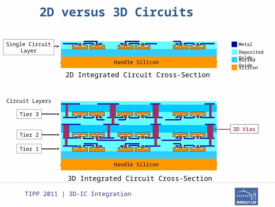
2D versus 3D Circuits
3D Integrated Circuit Cross-Section
2D Integrated Circuit Cross-Section
Handle Silicon
Single CircuitLayer
Circuit Layers
Tier 1
Tier 2
Tier 3
Handle Silicon
3D Vias
Silicon
Buried Oxide
Deposited Oxide
Metal

TIPP 2011 | 3D-IC Integration
Tier2-to-Tier1 Alignment and Bonding
Handle Silicon
Buried Oxide
Tier-1
Handle Silicon
Buried Oxide
Tier-2
Silicon
Buried Oxide
Deposited Oxide
Metal

TIPP 2011 | 3D-IC Integration
Tier2 Substrate Removal andElectrical Connection to Tier1
Handle Silicon
Buried Oxide
Tier-1Handle Silicon
Buried Oxide
Tier-2
Silicon
Buried Oxide
Deposited Oxide
Metal
Tungsten

TIPP 2011 | 3D-IC Integration
Tier3 Bonding and Alignment
Handle Silicon
Buried Oxide
Tier-1
Handle Silicon
Buried Oxide
Tier-3
Silicon
Buried Oxide
Deposited Oxide
Metal
Tungsten

TIPP 2011 | 3D-IC Integration
Tezzaron 3D MPW Run ExperienceAssume identical wafers
Flip 2nd wafer ontop of second wafer
Bond 2nd wafer to 1st
wafer using Cu-Cuthermocompression bond
Thin 2nd wafer to about 12um to expose super via
Add metallizationto back of 2nd waferfor bump or wirebond
After FEOLfabricate6 um supercontact (via)
CompleteBEOL processing 12 um
Additional waferscan be stacked face to back on top of 2nd wafer
TSV
6um
Cu-Cubond
• In late 2008, consortium of 15 institutions formed to fabricated 3D integrated circuits using the Tezzaron/Chartered process.
– Chartered uses a via middle process to add vias to 130nm CMOS process
– Tezzaron performs 3D stacking using Cu-Cu thermo compression bonding

TIPP 2011 | 3D-IC Integration
VTTFrauenhofer IZM
IMECFrauenhofer EMFT
CEA LETI(CMP)
CNM
Possibilities offered by European Industry and Research Institutes
8
Top Related