


Languages
Pages
Legal


Proposal for 400GE Optical PMDs for
SMF Objectives based on 4 x 100G DMT David Lewis, Sacha Corbeil, Beck Mason
2
- 10km objectives (400GBASE-LR4) covered in takahara_3bs_01_1114
- This presentation provides the baseline proposals for
- 500 m reach on parallel SMF (400GBASE-PSM4)
- 2 km reach on duplex SMF (400GBASE-FR4)
Summary
3
- Hisaya Sakamoto, Fujitsu Optical Components
- Hideki Isono, Fujitsu Optical Components
- Tomoo Takahara, Fujitsu Optical Components
- Toshiki Tanaka, Fujitsu
- Brian Tiepen, Adva Optical
- Moonsoo Park, OE-Solution
- YK Park, OE-Solution
- Ian Dedic, Fujitsu Semiconductor
- Patricia Bower, Fujitsu Semiconductor
- Bernd Nebendahl, Keysight Technologies
- Rolf Steiner, Keysight Technologies
Supporters and Contributors

4
PMD Block Diagram – for Parallel SMF (500 m reach)

5
PMD Block Diagram – for Duplex SMF (2 and 10 km reach)

6
Description 400GBASE-PSM4 400GBASE-FR4 400GBASE-LR4 Unit Note
Input signaling rate, each lane (range) 103.125 +/-100 ppm Gb/s
Output signaling rate, each lane (range) 116.015625 +/-100 ppm Gb/s
Lane wavelengths (range) 1260 - 1355 1294.53 to 1296.59 1299.02 to 1301.09 1303.54 to 1305.63 1308.09 to 1310.19
nm
Average launch power, each lane (max) 1.5 4.0 TBD dBm
Average launch power, each lane (min) -1.5 1.0 2.8 dBm
Dispersion and MPI penalties, each lane (max) 1.0 1.0 1.0 dB
RIN, each lane, average (max) -145 -145 -148 dB/Hz
Optical return loss tolerance (max) 20 20 dB
Transmitter reflectance (max) -26 -26 -26 dB
Optical modulation index 0.45
Clipping Ratio (of numerical transmit data) 3.16 3.16 3.16 Tolerance TBD*
Cascaded Tx 3 dB electrical upper cutoff frequency (min) 15 15 15 GHz Informative
Total harmonic distortion (max) 2 2 2 % TBR
Effective number of bits for DAC 6 (TBR) 6 (TBR) 6 (TBR) bit Informative
Transmitter Optical Specifications at TP2
Additional notes & definitions
* Clipping Ratio: Defined here as the ratio to be maintained, by design, at the numerical generation of data at the transmitter, (i.e. prior to conversion to a voltage).
RatioClipping = 𝑅𝑎𝑛𝑔𝑒𝐷𝐴𝐶2∙𝜎𝐷𝑎𝑡𝑎
=2#𝑏𝑖𝑡𝑠
2∙𝜎𝐷𝑎𝑡𝑎
=2(#𝑏𝑖𝑡𝑠−1)
𝜎𝐷𝑎𝑡𝑎
-100 -50 0 50 100
0
500
1000
1500
2000
2500
Numerical value of DMT Signal prior to DAC
Definition of Clipping Ratio
D=s
N=½ DAC-Range
RatioClipping = N / D

7
Receiver Optical Specifications at TP3
Description 400GBASE-PSM4 400GBASE-FR4 400GBASE-LR4 Unit Note
Input signaling rate, each lane (range) 116.015625 +/-100 ppm Gb/s
Output signaling rate, each lane (range) 103.125 +/-100 ppm Gb/s
Lane wavelengths (range) 1260 - 1355 1294.53 to 1296.59 1299.02 to 1301.09 1303.54 to 1305.63 1308.09 to 1310.19
nm
Damage threshold (min) 5.0 7.0 dBm
Average receive power, each lane (max) 1.5 4.0 dBm
Average receive power, each lane (min) -5.5 -4.0 -5.0 dBm *
Receiver reflectance (max) -26 dB
Receiver sensitivity (max) -6.5 -5 dBm **
Reference BER 3.3e-3 FEC threshold
Cascaded Rx 3dB electrical upper cutoff frequency (min) 15 GHz informative
Total harmonic distortion, per component 2 (TBR) % informative
Effective number of bits for ADC 5.5 (TBR) bit informative
* Measured over fiber with worst-case transmission penalties included at reference BER.
** Measured in back-to-back condition (no dispersion), with typical Tx, at reference BER.

8
Optical Link Budgets
Description 400GBASE-PSM4 400GBASE-FR4 400GBASE-LR4 Unit Note
Power budget at maximum TDP 5 6 7.8 dB
Operating distance 500 2000 10000 m
Channel insertion loss 4 5 6.3 dB
Allocation for penalties 1 1 1.5 dB
Additional insertion loss allowed 0 0 0 dB
Min / Max average power in dBm for 2 km case

9
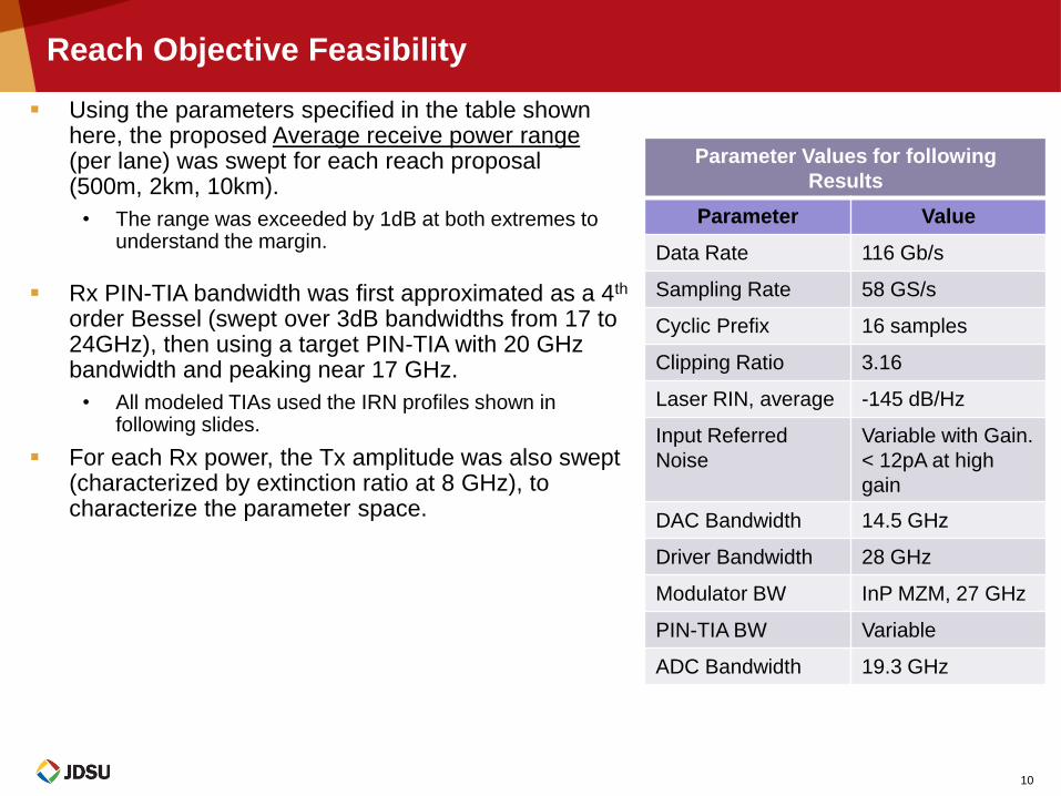
The proposed reach objectives were verified in terms of sensitivity performance through noise modeling.
The noise model takes into account the frequency response of all components in the transmission-chain, as well as noise contributions, and develops an SNR spectrum and DMT BER prediction.
Reach Objective Feasibility
SNR spectrum and BER predictions correlate well with existing hardware measurements using both a DMT test-chip, as well as earlier DAC/ADC DMT implementations.
10
Rx PIN-TIA bandwidth was first approximated as a 4th order Bessel (swept over 3dB bandwidths from 17 to 24GHz), then using a target PIN-TIA with 20 GHz bandwidth and peaking near 17 GHz.
• All modeled TIAs used the IRN profiles shown in following slides.
For each Rx power, the Tx amplitude was also swept (characterized by extinction ratio at 8 GHz), to characterize the parameter space.
Reach Objective Feasibility
Parameter Values for following
Results
Parameter Value
Data Rate 116 Gb/s
Sampling Rate 58 GS/s
Cyclic Prefix 16 samples
Clipping Ratio 3.16
Laser RIN, average -145 dB/Hz
Input Referred
Noise
Variable with Gain.
< 12pA at high
gain
DAC Bandwidth 14.5 GHz
Driver Bandwidth 28 GHz
Modulator BW InP MZM, 27 GHz
PIN-TIA BW Variable
ADC Bandwidth 19.3 GHz
Using the parameters specified in the table shown here, the proposed Average receive power range (per lane) was swept for each reach proposal (500m, 2km, 10km).
• The range was exceeded by 1dB at both extremes to understand the margin.

11
Off-the-shelf 100G-LR4 1310nm Transmitter
Actual measured SNR and BER results used to calibrate the DMT system model
Predicted SNR shows close agreement with measured SNR.
Worst noise contributor is laser RIN, fol’d by harmonics from EA Modulator non-linearity then ADC & thermal
• Integrated RIN of this device is -145 with a peak at -138 dB/Hz
• Dip seen ~7GHz is due to RIN peak.
Measured SNR data with 1310 EML
Hardware 28nm DAC/ADC
Samp-Rate 63 GS/s
Data-Rate 116 Gb/s
Source EML-TOSA DFB
Modulator EML-TOSA EA
Ext-Ratio (8GHz) Estimated at 8dB
Receiver Disco R409
Rx Pwr 0.5 dBm
Meas BER 4.6e-4

12
We have demonstrated live-traffic 100G/λ DMT transmission using directly modulated 25G DFB lasers, EMLs, and MZMs
• Traffic and BER performance were shown to be stable over >12 hour test
• BER as low as 4E-5 demonstrated with MZM in a back-to-back configuration
• Work showed that any of the three transmitter types could be used in the DMT application
For the noise modeling in this proposal we have used an InP DFB-MZM frequency response and EO transfer function.
Tx Used for Modeling: DFB-MZ

13
One improvement required to enable DMT and other higher-order modulation formats for 400GE is lower IRN (tipper_3bs_01a_0914)
TIA with IRN < 12pA/√Hz for gain > 1 kW is possible, and has been used in following results.
* Information in above charts courtesy of Semtech.
Rx: PIN-TIA
14
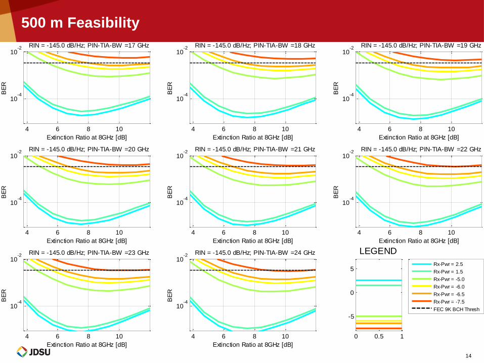
500 m Feasibility
4 6 8 10
10-4
10-2 RIN = -145.0 dB/Hz; PIN-TIA-BW =17 GHz
BE
R
Extinction Ratio at 8GHz [dB]
4 6 8 10
10-4
10-2 RIN = -145.0 dB/Hz; PIN-TIA-BW =18 GHz
BE
R
Extinction Ratio at 8GHz [dB]
4 6 8 10
10-4
10-2 RIN = -145.0 dB/Hz; PIN-TIA-BW =19 GHz
BE
R
Extinction Ratio at 8GHz [dB]
4 6 8 10
10-4
10-2 RIN = -145.0 dB/Hz; PIN-TIA-BW =20 GHz
BE
R
Extinction Ratio at 8GHz [dB]
4 6 8 10
10-4
10-2 RIN = -145.0 dB/Hz; PIN-TIA-BW =21 GHz
BE
R
Extinction Ratio at 8GHz [dB]
4 6 8 10
10-4
10-2 RIN = -145.0 dB/Hz; PIN-TIA-BW =22 GHz
BE
R
Extinction Ratio at 8GHz [dB]
4 6 8 10
10-4
10-2 RIN = -145.0 dB/Hz; PIN-TIA-BW =23 GHz
BE
R
Extinction Ratio at 8GHz [dB]
4 6 8 10
10-4
10-2 RIN = -145.0 dB/Hz; PIN-TIA-BW =24 GHz
BE
R
Extinction Ratio at 8GHz [dB]
0 0.5 1
-5
0
5
LEGEND
Rx-Pwr = 2.5
Rx-Pwr = 1.5
Rx-Pwr = -5.0
Rx-Pwr = -6.0
Rx-Pwr = -6.5
Rx-Pwr = -7.5
FEC 9K BCH Thresh
15
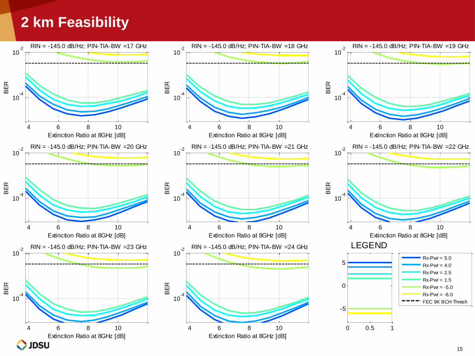
2 km Feasibility
4 6 8 10
10-4
10-2 RIN = -145.0 dB/Hz; PIN-TIA-BW =17 GHz
BE
R
Extinction Ratio at 8GHz [dB]
4 6 8 10
10-4
10-2 RIN = -145.0 dB/Hz; PIN-TIA-BW =18 GHz
BE
R
Extinction Ratio at 8GHz [dB]
4 6 8 10
10-4
10-2 RIN = -145.0 dB/Hz; PIN-TIA-BW =19 GHz
BE
R
Extinction Ratio at 8GHz [dB]
4 6 8 10
10-4
10-2 RIN = -145.0 dB/Hz; PIN-TIA-BW =20 GHz
BE
R
Extinction Ratio at 8GHz [dB]
4 6 8 10
10-4
10-2 RIN = -145.0 dB/Hz; PIN-TIA-BW =21 GHz
BE
R
Extinction Ratio at 8GHz [dB]
4 6 8 10
10-4
10-2 RIN = -145.0 dB/Hz; PIN-TIA-BW =22 GHz
BE
R
Extinction Ratio at 8GHz [dB]
4 6 8 10
10-4
10-2 RIN = -145.0 dB/Hz; PIN-TIA-BW =23 GHz
BE
R
Extinction Ratio at 8GHz [dB]
4 6 8 10
10-4
10-2 RIN = -145.0 dB/Hz; PIN-TIA-BW =24 GHz
BE
R
Extinction Ratio at 8GHz [dB]
0 0.5 1
-5
0
5
LEGEND
Rx-Pwr = 5.0
Rx-Pwr = 4.0
Rx-Pwr = 2.5
Rx-Pwr = 1.5
Rx-Pwr = -5.0
Rx-Pwr = -6.0
FEC 9K BCH Thresh

16
10 km Feasibility
4 6 8 10
10-4
10-2 RIN = -145.0 dB/Hz; PIN-TIA-BW =17 GHz
BE
R
Extinction Ratio at 8GHz [dB]
4 6 8 10
10-4
10-2 RIN = -145.0 dB/Hz; PIN-TIA-BW =18 GHz
BE
R
Extinction Ratio at 8GHz [dB]
4 6 8 10
10-4
10-2 RIN = -145.0 dB/Hz; PIN-TIA-BW =19 GHz
BE
R
Extinction Ratio at 8GHz [dB]
4 6 8 10
10-4
10-2 RIN = -145.0 dB/Hz; PIN-TIA-BW =20 GHz
BE
R
Extinction Ratio at 8GHz [dB]
4 6 8 10
10-4
10-2 RIN = -145.0 dB/Hz; PIN-TIA-BW =21 GHz
BE
R
Extinction Ratio at 8GHz [dB]
4 6 8 10
10-4
10-2 RIN = -145.0 dB/Hz; PIN-TIA-BW =22 GHz
BE
R
Extinction Ratio at 8GHz [dB]
4 6 8 10
10-4
10-2 RIN = -145.0 dB/Hz; PIN-TIA-BW =23 GHz
BE
R
Extinction Ratio at 8GHz [dB]
4 6 8 10
10-4
10-2 RIN = -145.0 dB/Hz; PIN-TIA-BW =24 GHz
BE
R
Extinction Ratio at 8GHz [dB]
0 0.5 1
-5
0
5
LEGEND
Rx-Pwr = 6.7
Rx-Pwr = 5.7
Rx-Pwr = 5.0
Rx-Pwr = 4.0
Rx-Pwr = 2.5
Rx-Pwr = 1.5
Rx-Pwr = -5.0
Rx-Pwr = -6.0
FEC 9K BCH Thresh

17
Target Receiver
500 m 2 km 10 km
0 0.5 1
-5
0
5
Rx-Pwr = 6.7
Rx-Pwr = 5.7
Rx-Pwr = 5.0
Rx-Pwr = 4.0
Rx-Pwr = 2.5
Rx-Pwr = 1.5
Rx-Pwr = -5.0
Rx-Pwr = -6.0
Rx-Pwr = -6.5
Rx-Pwr = -7.5
FEC 9K BCH Thresh
4 6 8 10
10-5
10-4
10-3
10-2
RIN = -145.0 dB/Hz; Target PIN(20GHz) with Low-IRN TIA
BE
R
Extinction Ratio at 8GHz [dB]
4 6 8 10
10-5
10-4
10-3
10-2
RIN = -145.0 dB/Hz; Target PIN(20GHz) with Low-IRN TIA
BE
R
Extinction Ratio at 8GHz [dB]
4 6 8 10
10-5
10-4
10-3
10-2
RIN = -145.0 dB/Hz; Target PIN(20GHz) with Low-IRN TIA
BE
R
Extinction Ratio at 8GHz [dB]

18
Feasibility Summary
-8 -6 -4 -2 0 2 4 6
10-5
10-4
10-3
10-2
Rx Average Input Power [dBm]
BE
R
Summary for IEEE 802.3bs 500m DMT Link Budget
PIN-TIA-BW =17GHz @ ER=9.3
PIN-TIA-BW =18GHz @ ER=10.2
PIN-TIA-BW =19GHz @ ER=9.3
PIN-TIA-BW =20GHz @ ER=10.2
PIN-TIA-BW =21GHz @ ER=9.3
PIN-TIA-BW =22GHz @ ER=9.3
PIN-TIA-BW =23GHz @ ER=9.3
PIN-TIA-BW =24GHz @ ER=9.3
Target PIN-TIA, 20GHz @ ER=9.3
FEC 9K BCH Thresh
Sensitivity Limit
-8 -6 -4 -2 0 2 4 6
10-5
10-4
10-3
10-2
Rx Average Input Power [dBm]
BE
R
Summary for IEEE 802.3bs 2km DMT Link Budget
PIN-TIA-BW =17GHz @ ER=10.2
PIN-TIA-BW =18GHz @ ER=10.2
PIN-TIA-BW =19GHz @ ER=10.2
PIN-TIA-BW =20GHz @ ER=10.2
PIN-TIA-BW =21GHz @ ER=10.2
PIN-TIA-BW =22GHz @ ER=10.2
PIN-TIA-BW =23GHz @ ER=10.2
PIN-TIA-BW =24GHz @ ER=10.2
Target PIN-TIA, 20GHz @ ER=9.3
FEC 9K BCH Thresh
Sensitivity Limit
-8 -6 -4 -2 0 2 4 6
10-5
10-4
10-3
10-2
Rx Average Input Power [dBm]
BE
R
Summary for IEEE 802.3bs 10km DMT Link Budget
PIN-TIA-BW =17GHz @ ER=10.2
PIN-TIA-BW =18GHz @ ER=10.2
PIN-TIA-BW =19GHz @ ER=10.2
PIN-TIA-BW =20GHz @ ER=10.2
PIN-TIA-BW =21GHz @ ER=10.2
PIN-TIA-BW =22GHz @ ER=10.2
PIN-TIA-BW =23GHz @ ER=10.2
PIN-TIA-BW =24GHz @ ER=10.2
Target PIN-TIA, 20GHz @ ER=9.3
FEC 9K BCH Thresh
Sensitivity Limit
Executive summary of results:
• With PIN-TIA bandwidth >= 19 GHz, including the target PIN-TIA, and selecting the proper transmitter amplitude, the receiver sensitivity level can always be achieved below the FEC threshold for each of the reach objectives.
• DMT is viable for the receive power ranges proposed for each reach objective (500 m, 2 km, 10 km)

19
Proposed baselines for 500 m SMF and 2 km SMF based on 4 x 100 Gb/s DMT
Noise and bandwidth models developed and verified by comparison to live-traffic experiments with several different transmitter types
Real receiver bandwidth and noise models at different gain settings used in verification analyses
Modeling supports the proposed link budgets
Conclusion
Top Related