


Languages
Pages
Legal

July 2009 Doc ID 2147 Rev 9 1/29
29
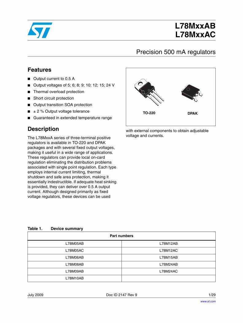
L78MxxABL78MxxAC
Precision 500 mA regulators
Features■ Output current to 0.5 A
■ Output voltages of 5; 6; 8; 9; 10; 12; 15; 24 V
■ Thermal overload protection
■ Short circuit protection
■ Output transition SOA protection
■ ± 2 % Output voltage tolerance
■ Guaranteed in extended temperature range
DescriptionThe L78MxxA series of three-terminal positive regulators is available in TO-220 and DPAK packages and with several fixed output voltages, making it useful in a wide range of applications. These regulators can provide local on-card regulation eliminating the distribution problems associated with single point regulation. Each type employs internal current limiting, thermal shutdown and safe area protection, making it essentially indestructible. If adequate heat sinking is provided, they can deliver over 0.5 A output current. Although designed primarily as fixed voltage regulators, these devices can be used
with external components to obtain adjustable voltage and currents.
DPAKTO-220
Table 1. Device summary
Part numbers
L78M05AB L78M12AB
L78M05AC L78M12AC
L78M06AB L78M15AB
L78M08AB L78M24AB
L78M09AB L78M24AC
L78M10AB
www.st.com
Contents L78MxxAB, L78MxxAC
2/29 Doc ID 2147 Rev 9
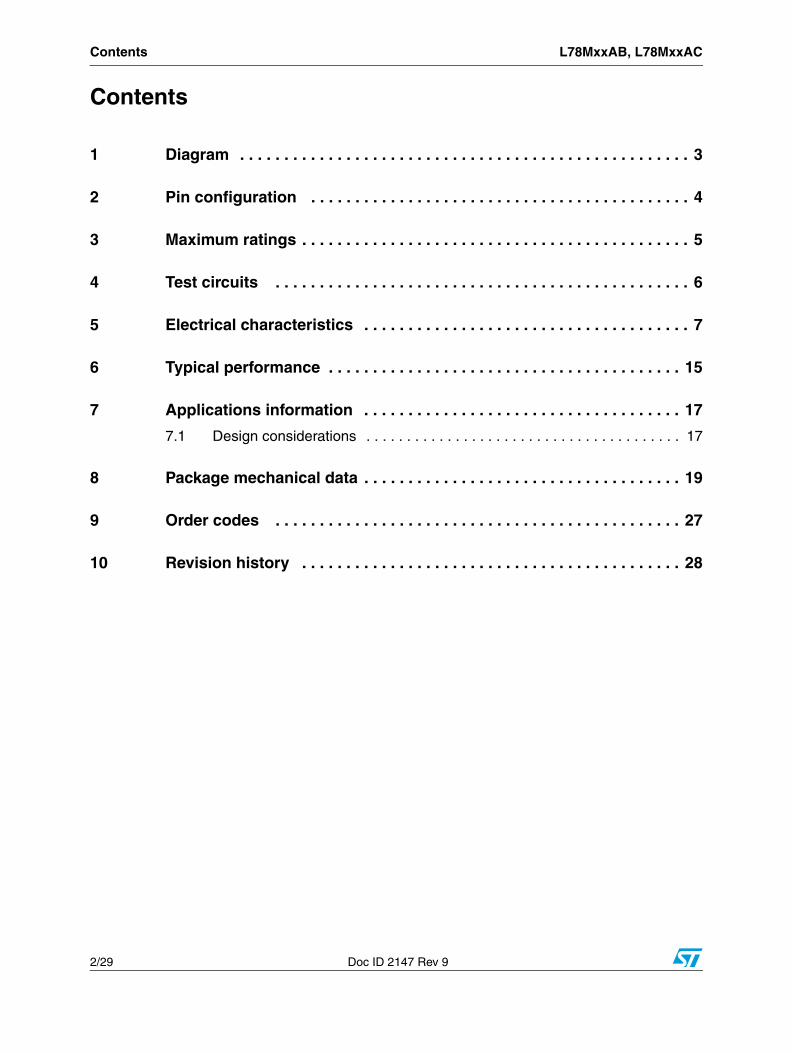
Contents
1 Diagram . . . . . . . . . . . . . . . . . . . . . . . . . . . . . . . . . . . . . . . . . . . . . . . . . . . 3
2 Pin configuration . . . . . . . . . . . . . . . . . . . . . . . . . . . . . . . . . . . . . . . . . . . 4
3 Maximum ratings . . . . . . . . . . . . . . . . . . . . . . . . . . . . . . . . . . . . . . . . . . . . 5
4 Test circuits . . . . . . . . . . . . . . . . . . . . . . . . . . . . . . . . . . . . . . . . . . . . . . . 6
5 Electrical characteristics . . . . . . . . . . . . . . . . . . . . . . . . . . . . . . . . . . . . . 7
6 Typical performance . . . . . . . . . . . . . . . . . . . . . . . . . . . . . . . . . . . . . . . . 15
7 Applications information . . . . . . . . . . . . . . . . . . . . . . . . . . . . . . . . . . . . 17
7.1 Design considerations . . . . . . . . . . . . . . . . . . . . . . . . . . . . . . . . . . . . . . . 17
8 Package mechanical data . . . . . . . . . . . . . . . . . . . . . . . . . . . . . . . . . . . . 19
9 Order codes . . . . . . . . . . . . . . . . . . . . . . . . . . . . . . . . . . . . . . . . . . . . . . 27
10 Revision history . . . . . . . . . . . . . . . . . . . . . . . . . . . . . . . . . . . . . . . . . . . 28
L78MxxAB, L78MxxAC Diagram
Doc ID 2147 Rev 9 3/29
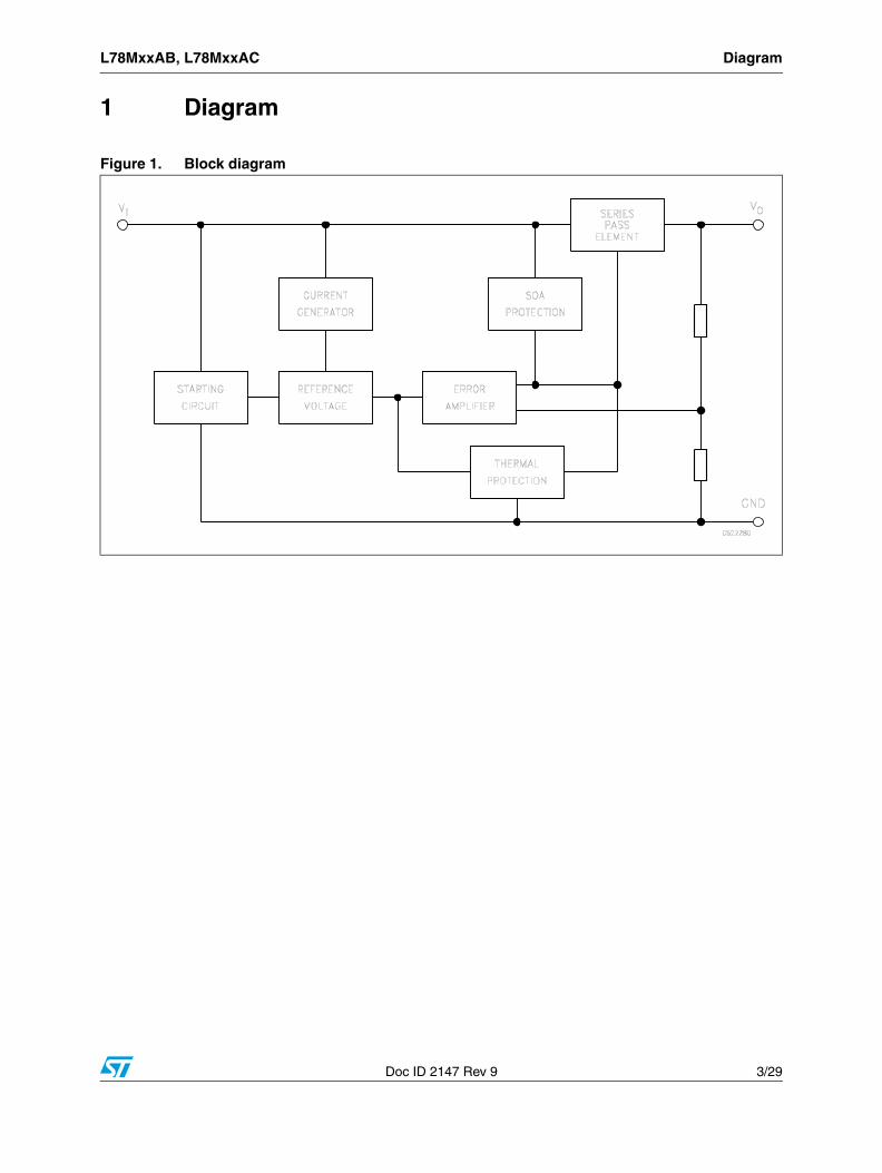
1 Diagram
Figure 1. Block diagram
Pin configuration L78MxxAB, L78MxxAC
4/29 Doc ID 2147 Rev 9
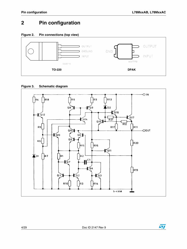
2 Pin configuration
Figure 2. Pin connections (top view)
DPAKTO-220
Figure 3. Schematic diagram
L78MxxAB, L78MxxAC Maximum ratings
Doc ID 2147 Rev 9 5/29
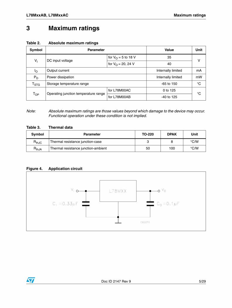
3 Maximum ratings
Note: Absolute maximum ratings are those values beyond which damage to the device may occur. Functional operation under these condition is not implied.
Table 2. Absolute maximum ratings
Symbol Parameter Value Unit
VI DC input voltagefor VO = 5 to 18 V 35
Vfor VO = 20, 24 V 40
IO Output current Internally limited mA
PD Power dissipation Internally limited mW
TSTG Storage temperature range -65 to 150 °C
TOP Operating junction temperature rangefor L78M00AC 0 to 125
°Cfor L78M00AB -40 to 125
Table 3. Thermal data
Symbol Parameter TO-220 DPAK Unit
RthJC Thermal resistance junction-case 3 8 °C/W
RthJA Thermal resistance junction-ambient 50 100 °C/W
Figure 4. Application circuit
Test circuits L78MxxAB, L78MxxAC
6/29 Doc ID 2147 Rev 9
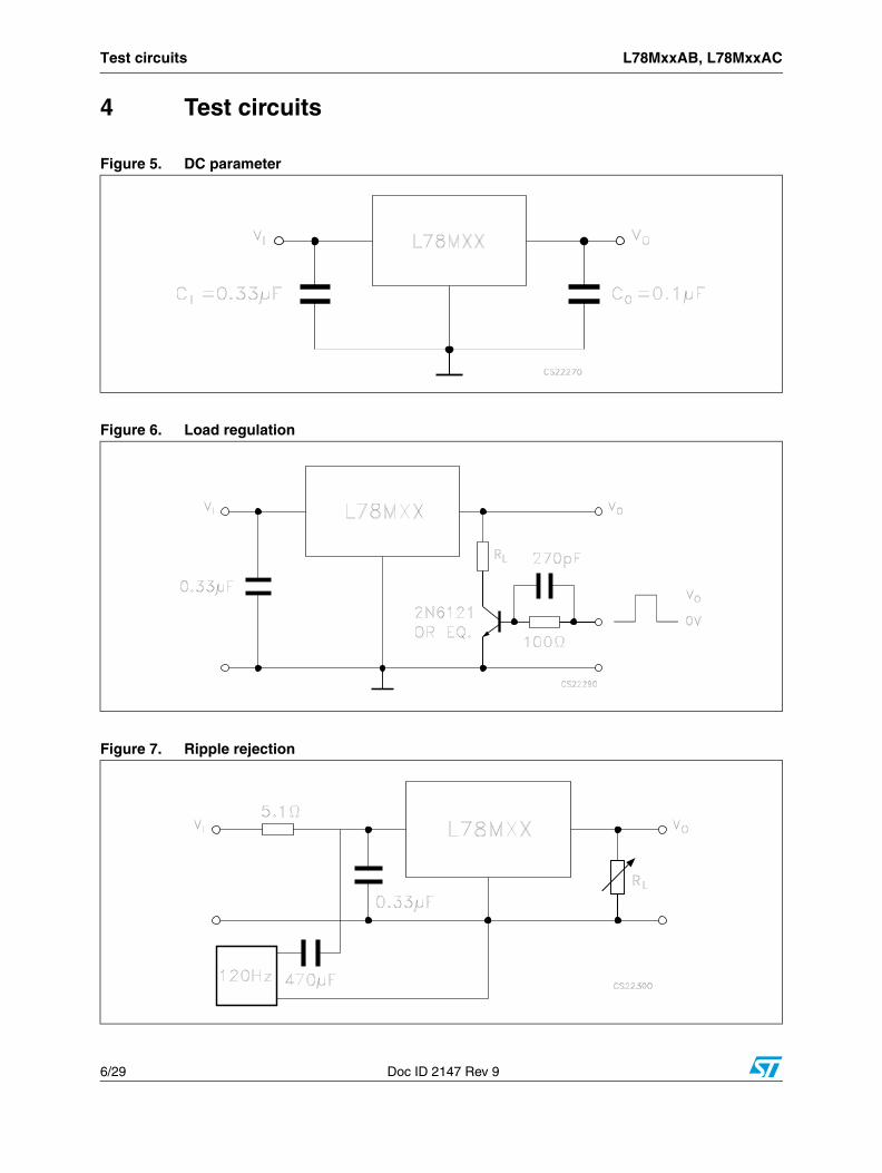
4 Test circuits
Figure 5. DC parameter
Figure 6. Load regulation
Figure 7. Ripple rejection
L78MxxAB, L78MxxAC Electrical characteristics
Doc ID 2147 Rev 9 7/29
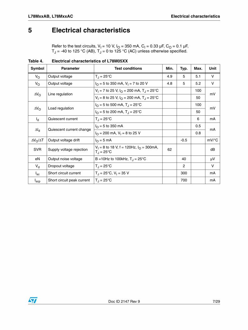
5 Electrical characteristics
Refer to the test circuits, VI = 10 V, IO = 350 mA, CI = 0.33 µF, CO = 0.1 µF, TJ = -40 to 125 °C (AB), TJ = 0 to 125 °C (AC) unless otherwise specified.
Table 4. Electrical characteristics of L78M05XX
Symbol Parameter Test conditions Min. Typ. Max. Unit
VO Output voltage TJ = 25°C 4.9 5 5.1 V
VO Output voltage IO = 5 to 350 mA, VI = 7 to 20 V 4.8 5 5.2 V
ΔVO Line regulationVI = 7 to 25 V, IO = 200 mA, TJ = 25°C 100
mVVI = 8 to 25 V, IO = 200 mA, TJ = 25°C 50
ΔVO Load regulationIO = 5 to 500 mA, TJ = 25°C 100
mVIO = 5 to 200 mA, TJ = 25°C 50
Id Quiescent current TJ = 25°C 6 mA
ΔId Quiescent current changeIO = 5 to 350 mA 0.5
mAIO = 200 mA, VI = 8 to 25 V 0.8
ΔVO/ΔT Output voltage drift IO = 5 mA -0.5 mV/°C
SVR Supply voltage rejectionVI = 8 to 18 V, f = 120Hz, IO = 300mA, TJ = 25°C
62 dB
eN Output noise voltage B =10Hz to 100kHz, TJ = 25°C 40 µV
Vd Dropout voltage TJ = 25°C 2 V
Isc Short circuit current TJ = 25°C, VI = 35 V 300 mA
Iscp Short circuit peak current TJ = 25°C 700 mA
Electrical characteristics L78MxxAB, L78MxxAC
8/29 Doc ID 2147 Rev 9
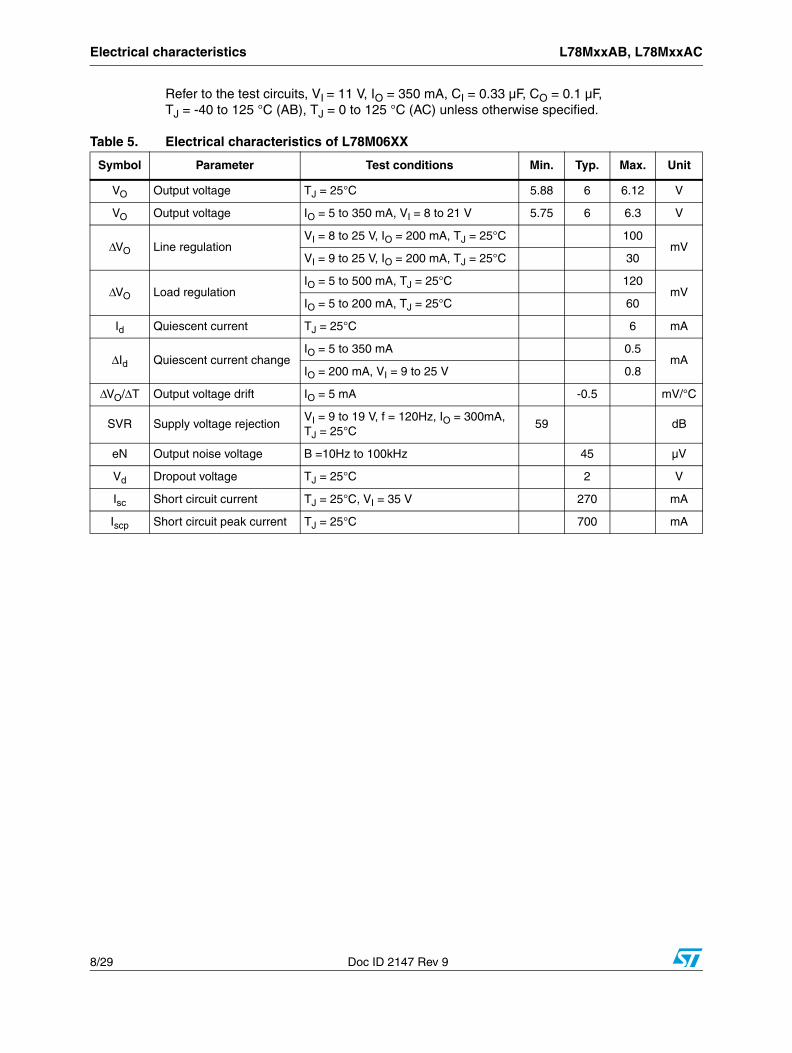
Refer to the test circuits, VI = 11 V, IO = 350 mA, CI = 0.33 µF, CO = 0.1 µF, TJ = -40 to 125 °C (AB), TJ = 0 to 125 °C (AC) unless otherwise specified.
Table 5. Electrical characteristics of L78M06XX
Symbol Parameter Test conditions Min. Typ. Max. Unit
VO Output voltage TJ = 25°C 5.88 6 6.12 V
VO Output voltage IO = 5 to 350 mA, VI = 8 to 21 V 5.75 6 6.3 V
ΔVO Line regulationVI = 8 to 25 V, IO = 200 mA, TJ = 25°C 100
mVVI = 9 to 25 V, IO = 200 mA, TJ = 25°C 30
ΔVO Load regulationIO = 5 to 500 mA, TJ = 25°C 120
mVIO = 5 to 200 mA, TJ = 25°C 60
Id Quiescent current TJ = 25°C 6 mA
ΔId Quiescent current changeIO = 5 to 350 mA 0.5
mAIO = 200 mA, VI = 9 to 25 V 0.8
ΔVO/ΔT Output voltage drift IO = 5 mA -0.5 mV/°C
SVR Supply voltage rejectionVI = 9 to 19 V, f = 120Hz, IO = 300mA, TJ = 25°C
59 dB
eN Output noise voltage B =10Hz to 100kHz 45 µV
Vd Dropout voltage TJ = 25°C 2 V
Isc Short circuit current TJ = 25°C, VI = 35 V 270 mA
Iscp Short circuit peak current TJ = 25°C 700 mA
L78MxxAB, L78MxxAC Electrical characteristics
Doc ID 2147 Rev 9 9/29
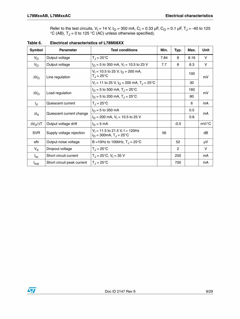
Refer to the test circuits, VI = 14 V, IO = 350 mA, CI = 0.33 µF, CO = 0.1 µF, TJ = -40 to 125 °C (AB), TJ = 0 to 125 °C (AC) unless otherwise specified).
Table 6. Electrical characteristics of L78M08XX
Symbol Parameter Test conditions Min. Typ. Max. Unit
VO Output voltage TJ = 25°C 7.84 8 8.16 V
VO Output voltage IO = 5 to 350 mA, VI = 10.5 to 23 V 7.7 8 8.3 V
ΔVO Line regulation
VI = 10.5 to 25 V, IO = 200 mA,TJ = 25°C
100mV
VI = 11 to 25 V, IO = 200 mA, TJ = 25°C 30
ΔVO Load regulationIO = 5 to 500 mA, TJ = 25°C 160
mVIO = 5 to 200 mA, TJ = 25°C 80
Id Quiescent current TJ = 25°C 6 mA
ΔId Quiescent current changeIO = 5 to 350 mA 0.5
mAIO = 200 mA, VI = 10.5 to 25 V 0.8
ΔVO/ΔT Output voltage drift IO = 5 mA -0.5 mV/°C
SVR Supply voltage rejectionVI = 11.5 to 21.5 V, f = 120HzIO = 300mA, TJ = 25°C
56 dB
eN Output noise voltage B =10Hz to 100kHz, TJ = 25°C 52 µV
Vd Dropout voltage TJ = 25°C 2 V
Isc Short circuit current TJ = 25°C, VI = 35 V 250 mA
Iscp Short circuit peak current TJ = 25°C 700 mA
Electrical characteristics L78MxxAB, L78MxxAC
10/29 Doc ID 2147 Rev 9
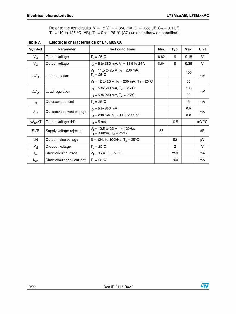
Refer to the test circuits, VI = 15 V, IO = 350 mA, CI = 0.33 µF, CO = 0.1 µF, TJ = -40 to 125 °C (AB), TJ = 0 to 125 °C (AC) unless otherwise specified).
Table 7. Electrical characteristics of L78M09XX
Symbol Parameter Test conditions Min. Typ. Max. Unit
VO Output voltage TJ = 25°C 8.82 9 9.18 V
VO Output voltage IO = 5 to 350 mA, VI = 11.5 to 24 V 8.64 9 9.36 V
ΔVO Line regulation
VI = 11.5 to 25 V, IO = 200 mA,TJ = 25°C
100mV
VI = 12 to 25 V, IO = 200 mA, TJ = 25°C 30
ΔVO Load regulationIO = 5 to 500 mA, TJ = 25°C 180
mVIO = 5 to 200 mA, TJ = 25°C 90
Id Quiescent current TJ = 25°C 6 mA
ΔId Quiescent current changeIO = 5 to 350 mA 0.5
mAIO = 200 mA, VI = 11.5 to 25 V 0.8
ΔVO/ΔT Output voltage drift IO = 5 mA -0.5 mV/°C
SVR Supply voltage rejectionVI = 12.5 to 23 V, f = 120Hz, IO = 300mA, TJ = 25°C
56 dB
eN Output noise voltage B =10Hz to 100kHz, TJ = 25°C 52 µV
Vd Dropout voltage TJ = 25°C 2 V
Isc Short circuit current VI = 35 V, TJ = 25°C 250 mA
Iscp Short circuit peak current TJ = 25°C 700 mA
L78MxxAB, L78MxxAC Electrical characteristics
Doc ID 2147 Rev 9 11/29
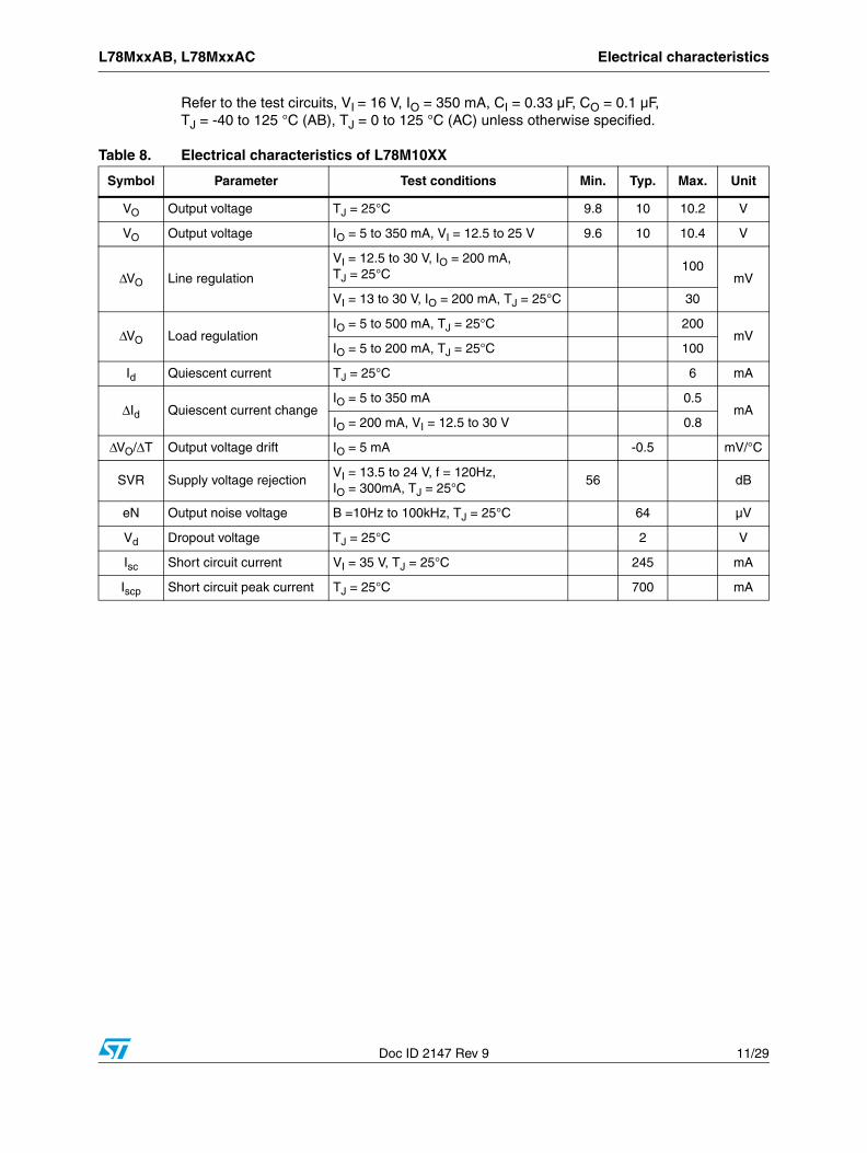
Refer to the test circuits, VI = 16 V, IO = 350 mA, CI = 0.33 µF, CO = 0.1 µF, TJ = -40 to 125 °C (AB), TJ = 0 to 125 °C (AC) unless otherwise specified.
Table 8. Electrical characteristics of L78M10XX
Symbol Parameter Test conditions Min. Typ. Max. Unit
VO Output voltage TJ = 25°C 9.8 10 10.2 V
VO Output voltage IO = 5 to 350 mA, VI = 12.5 to 25 V 9.6 10 10.4 V
ΔVO Line regulation
VI = 12.5 to 30 V, IO = 200 mA,TJ = 25°C
100mV
VI = 13 to 30 V, IO = 200 mA, TJ = 25°C 30
ΔVO Load regulationIO = 5 to 500 mA, TJ = 25°C 200
mVIO = 5 to 200 mA, TJ = 25°C 100
Id Quiescent current TJ = 25°C 6 mA
ΔId Quiescent current changeIO = 5 to 350 mA 0.5
mAIO = 200 mA, VI = 12.5 to 30 V 0.8
ΔVO/ΔT Output voltage drift IO = 5 mA -0.5 mV/°C
SVR Supply voltage rejectionVI = 13.5 to 24 V, f = 120Hz, IO = 300mA, TJ = 25°C
56 dB
eN Output noise voltage B =10Hz to 100kHz, TJ = 25°C 64 µV
Vd Dropout voltage TJ = 25°C 2 V
Isc Short circuit current VI = 35 V, TJ = 25°C 245 mA
Iscp Short circuit peak current TJ = 25°C 700 mA
Electrical characteristics L78MxxAB, L78MxxAC
12/29 Doc ID 2147 Rev 9
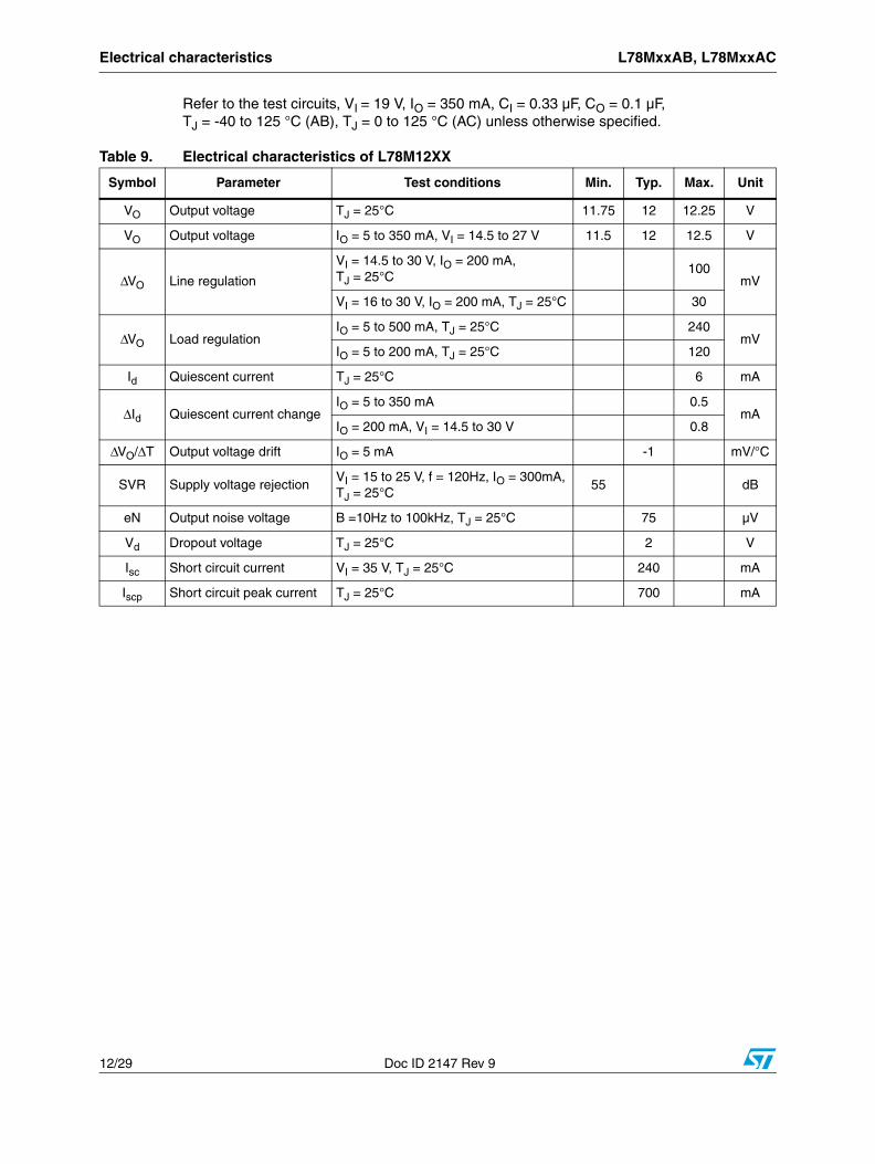
Refer to the test circuits, VI = 19 V, IO = 350 mA, CI = 0.33 µF, CO = 0.1 µF, TJ = -40 to 125 °C (AB), TJ = 0 to 125 °C (AC) unless otherwise specified.
Table 9. Electrical characteristics of L78M12XX
Symbol Parameter Test conditions Min. Typ. Max. Unit
VO Output voltage TJ = 25°C 11.75 12 12.25 V
VO Output voltage IO = 5 to 350 mA, VI = 14.5 to 27 V 11.5 12 12.5 V
ΔVO Line regulation
VI = 14.5 to 30 V, IO = 200 mA,TJ = 25°C
100mV
VI = 16 to 30 V, IO = 200 mA, TJ = 25°C 30
ΔVO Load regulationIO = 5 to 500 mA, TJ = 25°C 240
mVIO = 5 to 200 mA, TJ = 25°C 120
Id Quiescent current TJ = 25°C 6 mA
ΔId Quiescent current changeIO = 5 to 350 mA 0.5
mAIO = 200 mA, VI = 14.5 to 30 V 0.8
ΔVO/ΔT Output voltage drift IO = 5 mA -1 mV/°C
SVR Supply voltage rejectionVI = 15 to 25 V, f = 120Hz, IO = 300mA, TJ = 25°C
55 dB
eN Output noise voltage B =10Hz to 100kHz, TJ = 25°C 75 µV
Vd Dropout voltage TJ = 25°C 2 V
Isc Short circuit current VI = 35 V, TJ = 25°C 240 mA
Iscp Short circuit peak current TJ = 25°C 700 mA
L78MxxAB, L78MxxAC Electrical characteristics
Doc ID 2147 Rev 9 13/29
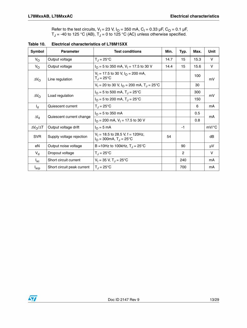
Refer to the test circuits, VI = 23 V, IO = 350 mA, CI = 0.33 µF, CO = 0.1 µF, TJ = -40 to 125 °C (AB), TJ = 0 to 125 °C (AC) unless otherwise specified.
Table 10. Electrical characteristics of L78M15XX
Symbol Parameter Test conditions Min. Typ. Max. Unit
VO Output voltage TJ = 25°C 14.7 15 15.3 V
VO Output voltage IO = 5 to 350 mA, VI = 17.5 to 30 V 14.4 15 15.6 V
ΔVO Line regulation
VI = 17.5 to 30 V, IO = 200 mA, TJ = 25°C
100mV
VI = 20 to 30 V, IO = 200 mA, TJ = 25°C 30
ΔVO Load regulationIO = 5 to 500 mA, TJ = 25°C 300
mVIO = 5 to 200 mA, TJ = 25°C 150
Id Quiescent current TJ = 25°C 6 mA
ΔId Quiescent current changeIO = 5 to 350 mA 0.5
mAIO = 200 mA, VI = 17.5 to 30 V 0.8
ΔVO/ΔT Output voltage drift IO = 5 mA -1 mV/°C
SVR Supply voltage rejectionVI = 18.5 to 28.5 V, f = 120Hz,IO = 300mA, TJ = 25°C
54 dB
eN Output noise voltage B =10Hz to 100kHz, TJ = 25°C 90 µV
Vd Dropout voltage TJ = 25°C 2 V
Isc Short circuit current VI = 35 V, TJ = 25°C 240 mA
Iscp Short circuit peak current TJ = 25°C 700 mA
Electrical characteristics L78MxxAB, L78MxxAC
14/29 Doc ID 2147 Rev 9
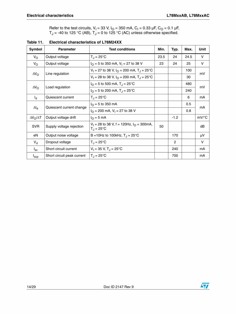
Refer to the test circuits, VI = 33 V, IO = 350 mA, CI = 0.33 µF, CO = 0.1 µF, TJ = -40 to 125 °C (AB), TJ = 0 to 125 °C (AC) unless otherwise specified.
Table 11. Electrical characteristics of L78M24XX
Symbol Parameter Test conditions Min. Typ. Max. Unit
VO Output voltage TJ = 25°C 23.5 24 24.5 V
VO Output voltage IO = 5 to 350 mA, VI = 27 to 38 V 23 24 25 V
ΔVO Line regulationVI = 27 to 38 V, IO = 200 mA, TJ = 25°C 100
mVVI = 28 to 38 V, IO = 200 mA, TJ = 25°C 30
ΔVO Load regulationIO = 5 to 500 mA, TJ = 25°C 480
mVIO = 5 to 200 mA, TJ = 25°C 240
Id Quiescent current TJ = 25°C 6 mA
ΔId Quiescent current changeIO = 5 to 350 mA 0.5
mAIO = 200 mA, VI = 27 to 38 V 0.8
ΔVO/ΔT Output voltage drift IO = 5 mA -1.2 mV/°C
SVR Supply voltage rejectionVI = 28 to 38 V, f = 120Hz, IO = 300mA, TJ = 25°C
50 dB
eN Output noise voltage B =10Hz to 100kHz, TJ = 25°C 170 µV
Vd Dropout voltage TJ = 25°C 2 V
Isc Short circuit current VI = 35 V, TJ = 25°C 240 mA
Iscp Short circuit peak current TJ = 25°C 700 mA
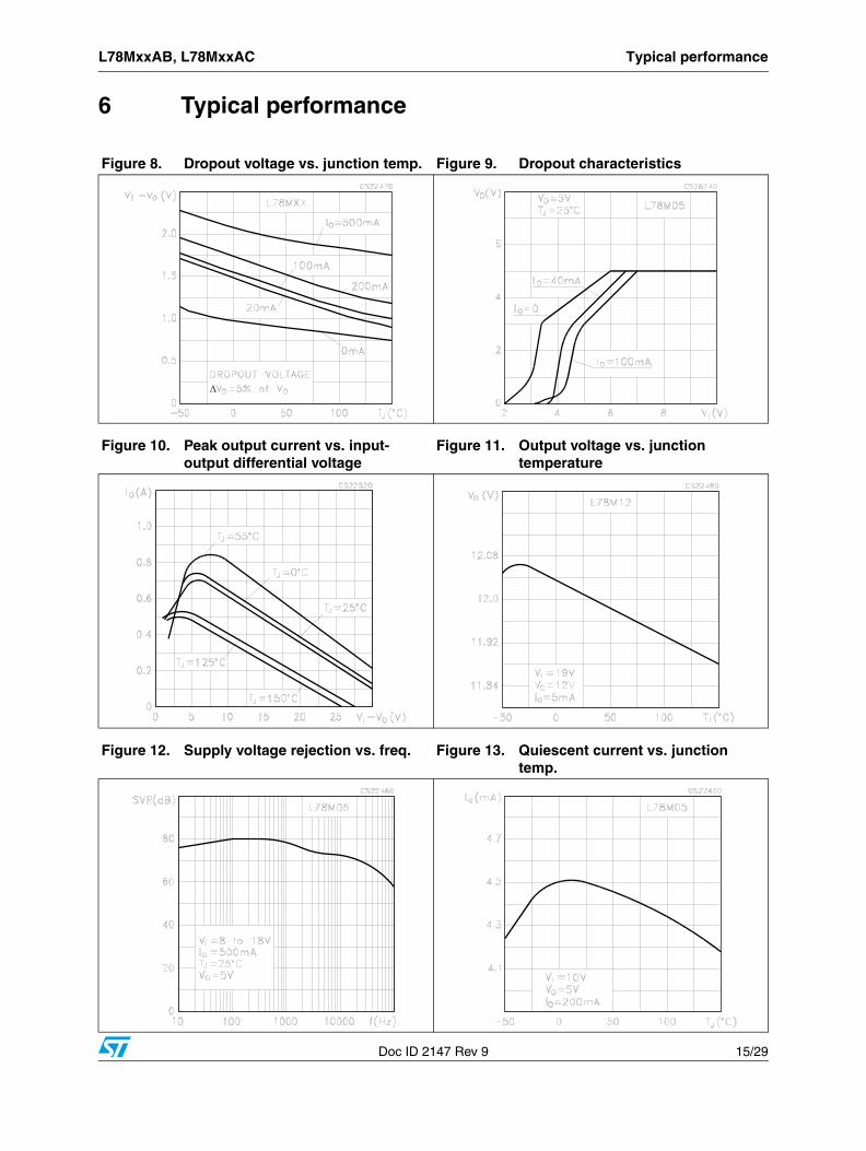
L78MxxAB, L78MxxAC Typical performance
Doc ID 2147 Rev 9 15/29
6 Typical performance
Figure 8. Dropout voltage vs. junction temp. Figure 9. Dropout characteristics
Figure 10. Peak output current vs. input-output differential voltage
Figure 11. Output voltage vs. junction temperature
Figure 12. Supply voltage rejection vs. freq. Figure 13. Quiescent current vs. junction temp.
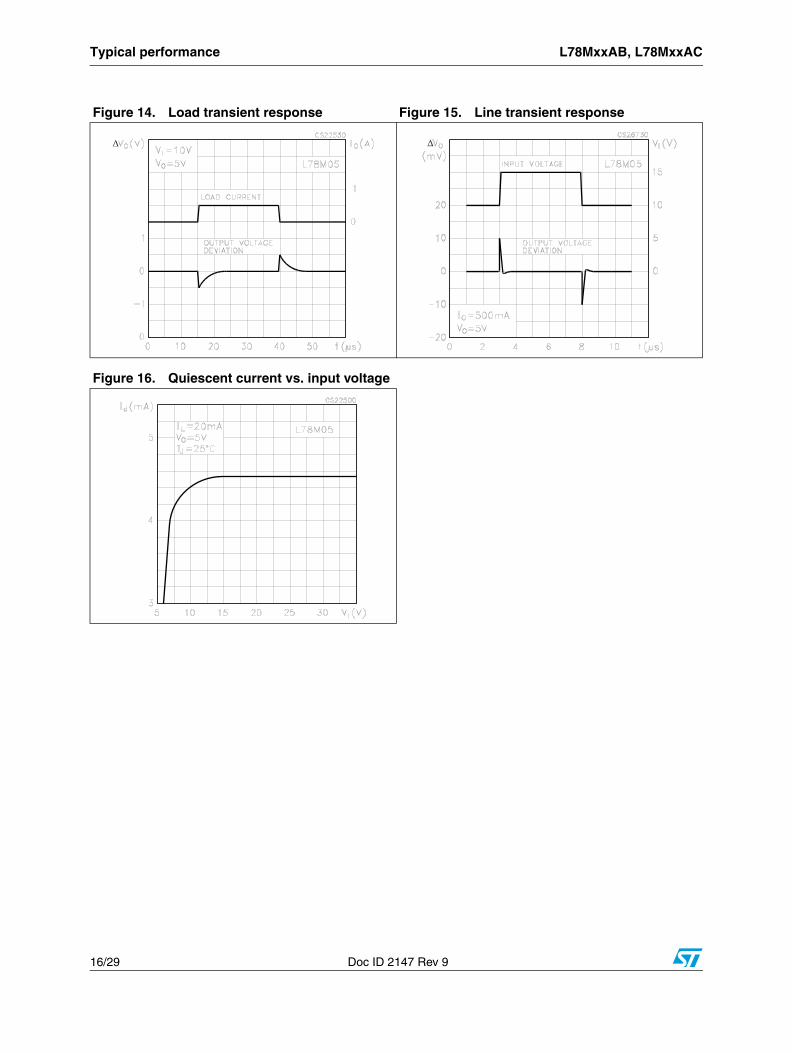
Typical performance L78MxxAB, L78MxxAC
16/29 Doc ID 2147 Rev 9
Figure 14. Load transient response Figure 15. Line transient response
Figure 16. Quiescent current vs. input voltage
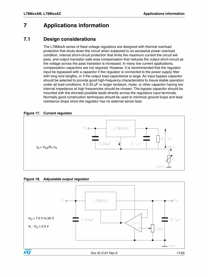
L78MxxAB, L78MxxAC Applications information
Doc ID 2147 Rev 9 17/29
7 Applications information
7.1 Design considerationsThe L78MxxA series of fixed voltage regulators are designed with thermal overload protection that shuts down the circuit when subjected to an excessive power overload condition, internal short-circuit protection that limits the maximum current the circuit will pass, and output transistor safe-area compensation that reduces the output short-circuit as the voltage across the pass transistor is increased. In many low current applications, compensation capacitors are not required. However, it is recommended that the regulator input be bypassed with a capacitor if the regulator is connected to the power supply filter with long wire lengths, or if the output load capacitance is large. An input bypass capacitor should be selected to provide good high-frequency characteristics to insure stable operation under all load conditions. A 0.33 µF or larger tantalum, mylar, or other capacitor having low internal impedance at high frequencies should be chosen. The bypass capacitor should be mounted with the shortest possible leads directly across the regulators input terminals. Normally good construction techniques should be used to minimize ground loops and lead resistance drops since the regulator has no external sense lead.
Figure 17. Current regulator
IO = VXX/R1+Id
Figure 18. Adjustable output regulator
VO = 7.0 V to 20 V
VI - VO ≥ 2.0 V
Applications information L78MxxAB, L78MxxAC
18/29 Doc ID 2147 Rev 9
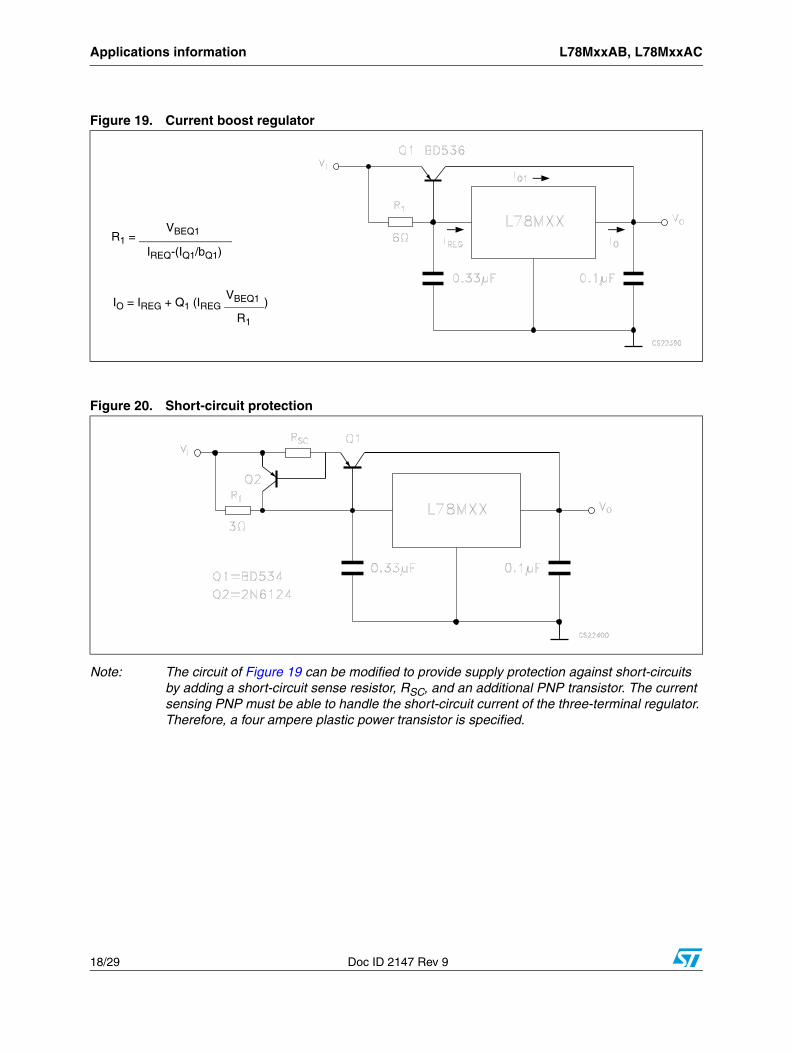
Note: The circuit of Figure 19 can be modified to provide supply protection against short-circuits by adding a short-circuit sense resistor, RSC, and an additional PNP transistor. The current sensing PNP must be able to handle the short-circuit current of the three-terminal regulator. Therefore, a four ampere plastic power transistor is specified.
Figure 19. Current boost regulator
IO = IREG + Q1 (IREG ______)VBEQ1
R1
R1 = ______________VBEQ1
IREQ-(IQ1/bQ1)
Figure 20. Short-circuit protection
L78MxxAB, L78MxxAC Package mechanical data
Doc ID 2147 Rev 9 19/29
8 Package mechanical data
In order to meet environmental requirements, ST offers these devices in different grades of ECOPACK® packages, depending on their level of environmental compliance. ECOPACK® specifications, grade definitions and product status are available at: www.st.com. ECOPACK is an ST trademark.
Package mechanical data L78MxxAB, L78MxxAC
20/29 Doc ID 2147 Rev 9
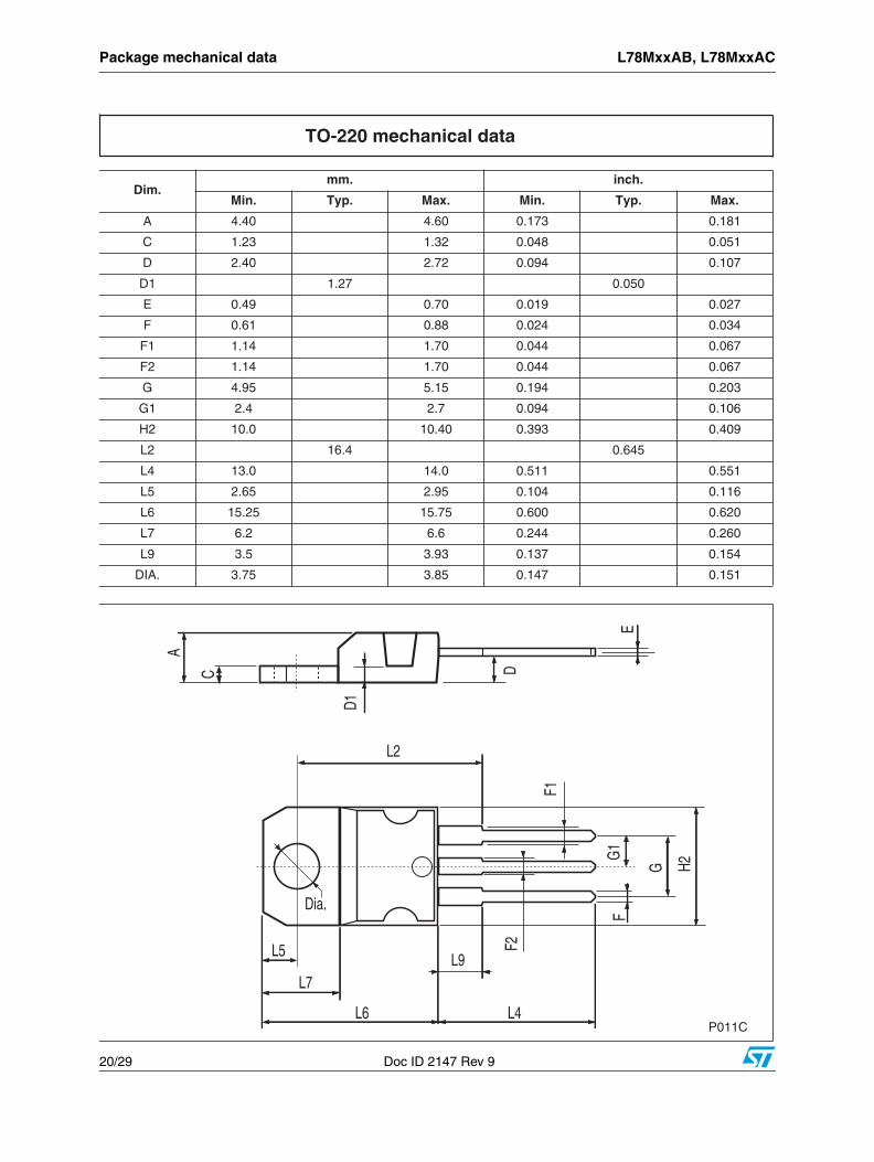
Dim.mm. inch.
Min. Typ. Max. Min. Typ. Max.
A 4.40 4.60 0.173 0.181
C 1.23 1.32 0.048 0.051
D 2.40 2.72 0.094 0.107
D1 1.27 0.050
E 0.49 0.70 0.019 0.027
F 0.61 0.88 0.024 0.034
F1 1.14 1.70 0.044 0.067
F2 1.14 1.70 0.044 0.067
G 4.95 5.15 0.194 0.203
G1 2.4 2.7 0.094 0.106
H2 10.0 10.40 0.393 0.409
L2 16.4 0.645
L4 13.0 14.0 0.511 0.551
L5 2.65 2.95 0.104 0.116
L6 15.25 15.75 0.600 0.620
L7 6.2 6.6 0.244 0.260
L9 3.5 3.93 0.137 0.154
DIA. 3.75 3.85 0.147 0.151
TO-220 mechanical data
P011C
L78MxxAB, L78MxxAC Package mechanical data
Doc ID 2147 Rev 9 21/29
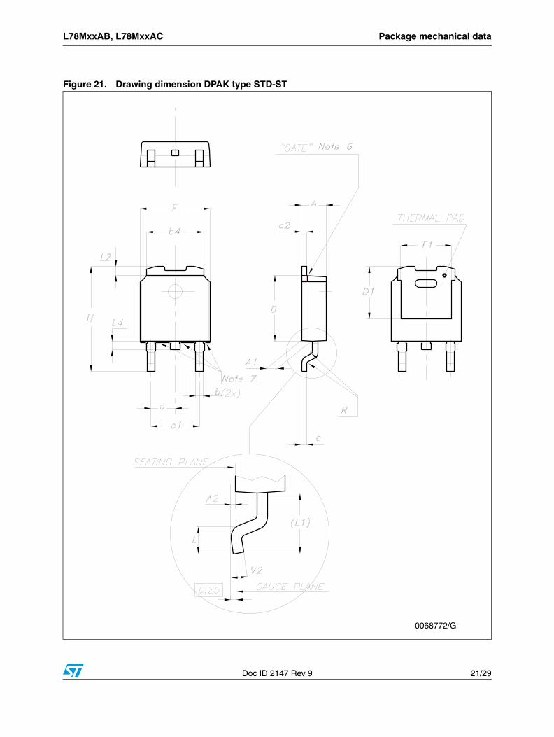
Figure 21. Drawing dimension DPAK type STD-ST
0068772/G
Package mechanical data L78MxxAB, L78MxxAC
22/29 Doc ID 2147 Rev 9
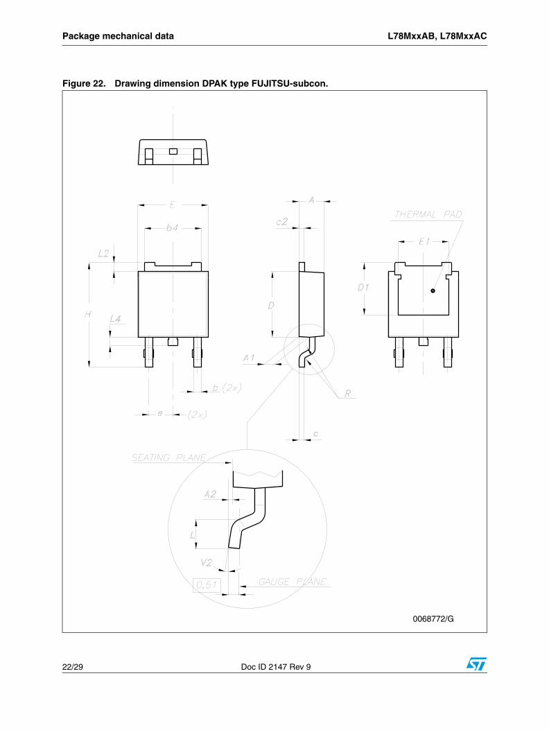
Figure 22. Drawing dimension DPAK type FUJITSU-subcon.
0068772/G
L78MxxAB, L78MxxAC Package mechanical data
Doc ID 2147 Rev 9 23/29
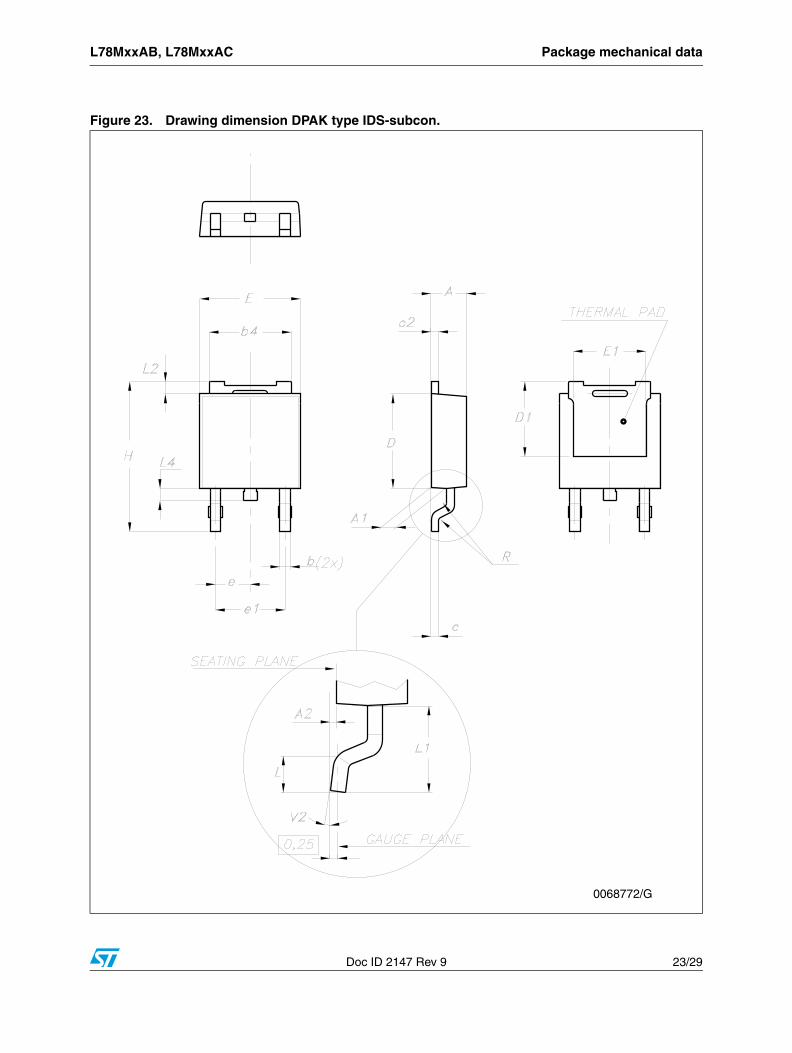
Figure 23. Drawing dimension DPAK type IDS-subcon.
0068772/G
Package mechanical data L78MxxAB, L78MxxAC
24/29 Doc ID 2147 Rev 9
Note: The DPAK package coming from the two subcontractors (Fujitsu and IDS) are fully compatible with the ST's package suggested footprint.
Table 12. DPAK mechanical data
Dim.
Type STD-ST Type Fujitsu-subcon. Type IDS-subcon.
mm. mm. mm.
Min. Typ. Max. Min. Typ. Max. Min. Typ. Max.
A 2.20 2.40 2.25 2.30 2.35 2.19 2.38
A1 0.90 1.10 0.96 1.06 0.89 1.14
A2 0.03 0.23 0 0.10 0.03 0.23
b 0.64 0.90 0.76 0.86 0.64 0.88
b4 5.20 5.40 5.28 5.38 5.21 5.46
c 0.45 0.60 0.46 0.56 0.46 0.58
c2 0.48 0.60 0.46 0.56 0.46 0.58
D 6.00 6.20 6.05 6.15 5.97 6.22
D1 5.10 5.27 5.47 5.20
E 6.40 6.60 6.55 6.60 6.65 6.35 6.73
E1 4.70 4.77 4.70
e 2.28 2.23 2.28 2.33 2.28
e1 4.40 4.60 4.51 4.61
H 9.35 10.10 9.90 10.30 9.40 10.42
L 1.00 1.40 1.60 0.90
L1 2.80 2.50 2.65
L2 0.80 1.03 1.13 0.89 1.27
L4 0.60 1.00 0.70 0.90 0.64 1.02
R 0.20 0.40 0.20
V2 0° 8° 0° 8° 0° 8°
L78MxxAB, L78MxxAC Package mechanical data
Doc ID 2147 Rev 9 25/29
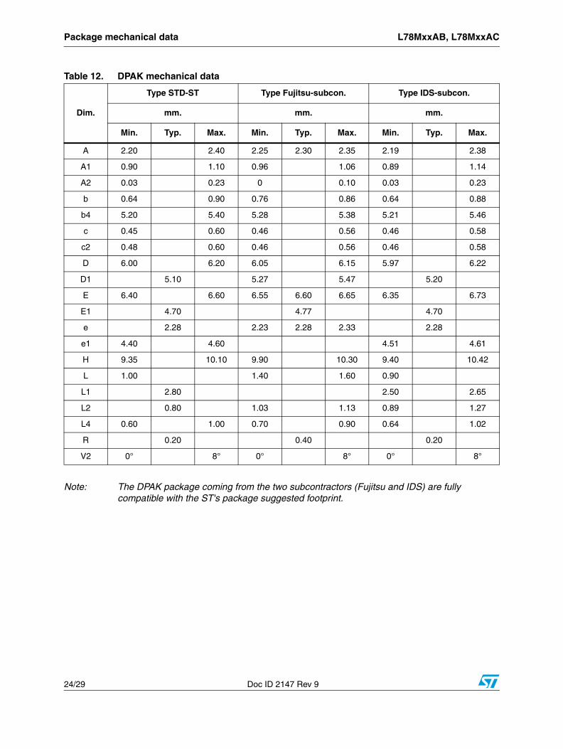
Figure 24. DPAK footprint recommended data
Table 13. Footprint data
Values
Dim. mm. inch.
A 6.70 0.264
B 6.70 0.64
C 1.8 0.070
D 3.0 0.118
E 1.60 0.063
F 2.30 0.091
G 2.30 0.091
Package mechanical data L78MxxAB, L78MxxAC
26/29 Doc ID 2147 Rev 9
Dim.mm. inch.
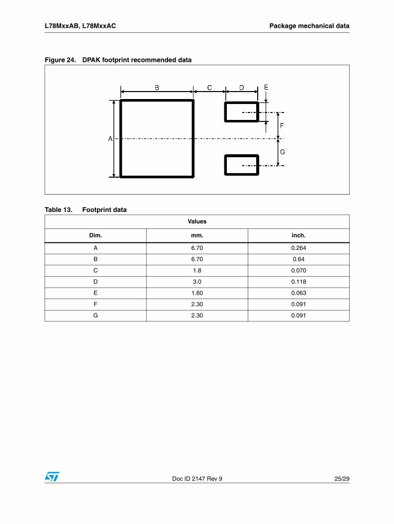
Min. Typ. Max. Min. Typ. Max.
A 330 12.992
C 12.8 13.0 13.2 0.504 0.512 0.519
D 20.2 0.795
N 60 2.362
T 22.4 0.882
Ao 6.80 6.90 7.00 0.268 0.272 0.2.76
Bo 10.40 10.50 10.60 0.409 0.413 0.417
Ko 2.55 2.65 2.75 0.100 0.104 0.105
Po 3.9 4.0 4.1 0.153 0.157 0.161
P 7.9 8.0 8.1 0.311 0.315 0.319
Tape & reel DPAK-PPAK mechanical data
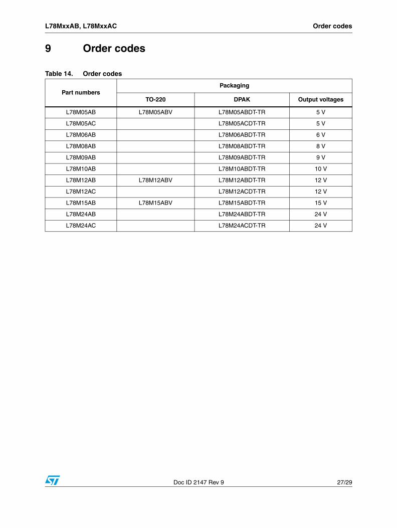
L78MxxAB, L78MxxAC Order codes
Doc ID 2147 Rev 9 27/29
9 Order codes
Table 14. Order codes
Part numbersPackaging
TO-220 DPAK Output voltages
L78M05AB L78M05ABV L78M05ABDT-TR 5 V
L78M05AC L78M05ACDT-TR 5 V
L78M06AB L78M06ABDT-TR 6 V
L78M08AB L78M08ABDT-TR 8 V
L78M09AB L78M09ABDT-TR 9 V
L78M10AB L78M10ABDT-TR 10 V
L78M12AB L78M12ABV L78M12ABDT-TR 12 V
L78M12AC L78M12ACDT-TR 12 V
L78M15AB L78M15ABV L78M15ABDT-TR 15 V
L78M24AB L78M24ABDT-TR 24 V
L78M24AC L78M24ACDT-TR 24 V
Revision history L78MxxAB, L78MxxAC
28/29 Doc ID 2147 Rev 9
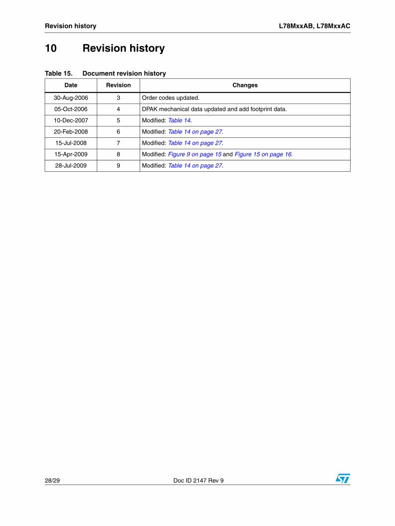
10 Revision history
Table 15. Document revision history
Date Revision Changes
30-Aug-2006 3 Order codes updated.
05-Oct-2006 4 DPAK mechanical data updated and add footprint data.
10-Dec-2007 5 Modified: Table 14.
20-Feb-2008 6 Modified: Table 14 on page 27.
15-Jul-2008 7 Modified: Table 14 on page 27.
15-Apr-2009 8 Modified: Figure 9 on page 15 and Figure 15 on page 16.
28-Jul-2009 9 Modified: Table 14 on page 27.
L78MxxAB, L78MxxAC
Doc ID 2147 Rev 9 29/29
Please Read Carefully:
Information in this document is provided solely in connection with ST products. STMicroelectronics NV and its subsidiaries (“ST”) reserve theright to make changes, corrections, modifications or improvements, to this document, and the products and services described herein at anytime, without notice.
All ST products are sold pursuant to ST’s terms and conditions of sale.
Purchasers are solely responsible for the choice, selection and use of the ST products and services described herein, and ST assumes noliability whatsoever relating to the choice, selection or use of the ST products and services described herein.
No license, express or implied, by estoppel or otherwise, to any intellectual property rights is granted under this document. If any part of thisdocument refers to any third party products or services it shall not be deemed a license grant by ST for the use of such third party productsor services, or any intellectual property contained therein or considered as a warranty covering the use in any manner whatsoever of suchthird party products or services or any intellectual property contained therein.
UNLESS OTHERWISE SET FORTH IN ST’S TERMS AND CONDITIONS OF SALE ST DISCLAIMS ANY EXPRESS OR IMPLIEDWARRANTY WITH RESPECT TO THE USE AND/OR SALE OF ST PRODUCTS INCLUDING WITHOUT LIMITATION IMPLIEDWARRANTIES OF MERCHANTABILITY, FITNESS FOR A PARTICULAR PURPOSE (AND THEIR EQUIVALENTS UNDER THE LAWSOF ANY JURISDICTION), OR INFRINGEMENT OF ANY PATENT, COPYRIGHT OR OTHER INTELLECTUAL PROPERTY RIGHT.
UNLESS EXPRESSLY APPROVED IN WRITING BY AN AUTHORIZED ST REPRESENTATIVE, ST PRODUCTS ARE NOTRECOMMENDED, AUTHORIZED OR WARRANTED FOR USE IN MILITARY, AIR CRAFT, SPACE, LIFE SAVING, OR LIFE SUSTAININGAPPLICATIONS, NOR IN PRODUCTS OR SYSTEMS WHERE FAILURE OR MALFUNCTION MAY RESULT IN PERSONAL INJURY,DEATH, OR SEVERE PROPERTY OR ENVIRONMENTAL DAMAGE. ST PRODUCTS WHICH ARE NOT SPECIFIED AS "AUTOMOTIVEGRADE" MAY ONLY BE USED IN AUTOMOTIVE APPLICATIONS AT USER’S OWN RISK.
Resale of ST products with provisions different from the statements and/or technical features set forth in this document shall immediately voidany warranty granted by ST for the ST product or service described herein and shall not create or extend in any manner whatsoever, anyliability of ST.
ST and the ST logo are trademarks or registered trademarks of ST in various countries.
Information in this document supersedes and replaces all information previously supplied.
The ST logo is a registered trademark of STMicroelectronics. All other names are the property of their respective owners.
© 2009 STMicroelectronics - All rights reserved
STMicroelectronics group of companies
Australia - Belgium - Brazil - Canada - China - Czech Republic - Finland - France - Germany - Hong Kong - India - Israel - Italy - Japan - Malaysia - Malta - Morocco - Philippines - Singapore - Spain - Sweden - Switzerland - United Kingdom - United States of America
www.st.com
Top Related