


Languages
Pages
Legal


ECE 1750
Week 4Week 4
RectifiersRectifiers
1

Rectifier• Rectifiers convert ac into dc• Rectifiers convert ac into dc
• Some commercial rectifiers:
(Used to charge batteries like those on the right)
2

Example of Assumed State AnalysisExample of Assumed State Analysis
++
+Vac
–RL–
•Consider the Vac > 0 case
W k i t lli t th t I i•We make an intelligent guess that I is flowing out of the source + node.
• If current is flowing, then the diode must be “on”g,
•We see that KVL (Vac = I • RL ) is satisfied
3
•Thus, our assumed state is correct
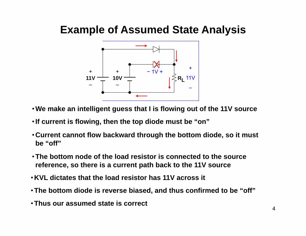
Example of Assumed State Analysis
+ ++ − 1V +10V
–RL 11V
–
11V–
1V
•We make an intelligent guess that I is flowing out of the 11V source
• If current is flowing, then the top diode must be “on”
C t t fl b k d th h th b tt di d it t
•The bottom node of the load resistor is connected to the source f th i t th b k t th 11V
•Current cannot flow backward through the bottom diode, so it must be “off”
reference, so there is a current path back to the 11V source
•KVL dictates that the load resistor has 11V across it
•The bottom diode is reverse biased, and thus confirmed to be “off”
4
The bottom diode is reverse biased, and thus confirmed to be off
•Thus our assumed state is correct

Assumed State Analysis+
1 3
RLWhat are the states of the diodes on or off?
–
+Vac–
4 2RL the diodes – on or off?
• Consider the Vac > 0 case
• We make an intelligent guess that I is flowing out of the source + node.g g g
• I cannot flow into diode #4, so diode #4 must be “off.” If current is flowing, then diode #1 must be “on.”
• I cannot flow into diode #3, so diode #3 must be “off.” I flows through RL.
• I comes to the junction of diodes #2 and #4. We have already determined
5
that diode #4 is “off.” If current is flowing, then diode #2 must be “on,” and I continues to the –Vac terminal.

Assumed State Analysis, cont.
1
RL+
++−
+Vac > 0
–
2RL+
− −
• A check of voltages confirms that diode #4 is indeed reverse biased as we have assumed
• We see that KVL (V = I • R ) is satisfied
• A check of voltages confirms that diode #3 is indeed reverse biased as we have assumed
• We see that KVL (Vac = I • RL ) is satisfied
• Thus, our assumed states are correct
6
• The same process can be repeated for Vac < 0, where it can be seen that diodes #3 and #4 are “on,” and diodes #1 and #2 are “off”
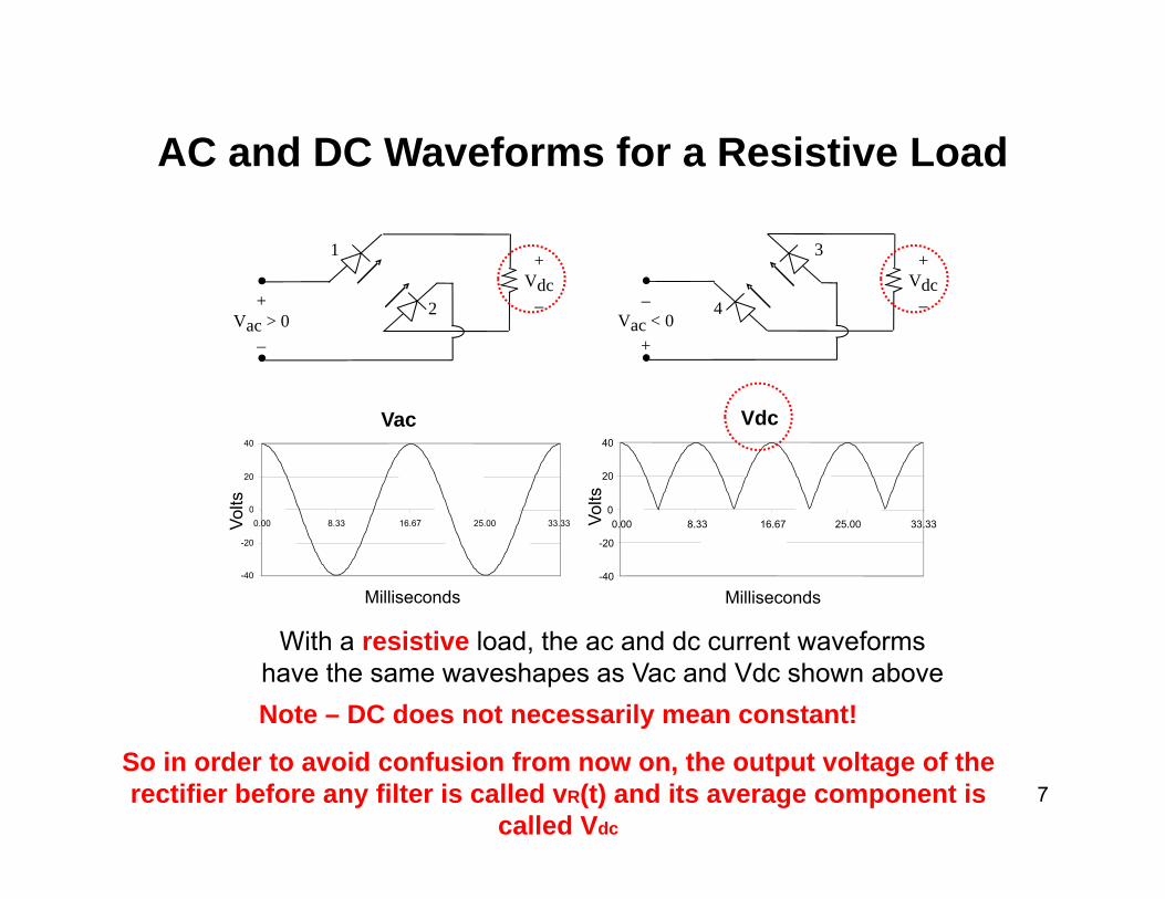
AC and DC Waveforms for a Resistive LoadC a d C a e o s o a es st e oad
1 +Vd
3 +Vd
+Vac > 0
–
2Vdc
– –Vac < 0
+
4Vdc
–
Vac
0
20
40
ts
Vdc
0
20
40
olts
-40
-20
00.00 8.33 16.67 25.00 33.33
Milliseconds
Vol
-40
-20
00.00 8.33 16.67 25.00 33.33
MillisecondsVo
With a resistive load, the ac and dc current waveforms have the same waveshapes as Vac and Vdc shown aboveNote – DC does not necessarily mean constant!
7So in order to avoid confusion from now on, the output voltage of the rectifier before any filter is called vR(t) and its average component is
called Vdc

Half-wave rectifier
0 0
1 sin( )2
T p pdc R
V VV v dt d
T
VpV
tt dcV
+Vac RL
+
8
––

Full wave rectifier
• Waveformsv
vR v
0 0
21 sin( )T p p
dc RV V
V v dt dT
V
t
dcVpV
tt
Rectifier 2nd order Filter
• Ideally: 2
, ,1, cos dcin rms in rms in out
VP V I PR

Diode Bridge Rectifier(DBR)
v vV ≈ 120√2V ≈ 170 V
Vdc≈ 120√2Vdc ≈ 170Vdc
Vp≈ 120√2Vdc ≈ 170 V
t
t
DC link+
1 3+
√Iac
DC link
–
+≈ 120Vac rms
–
4 2≈ 120√2Vdc ≈ 170Vdc−
First order
10
First order low pass
filter
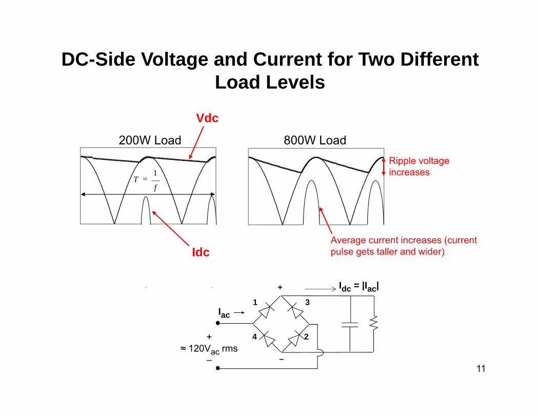
DC-Side Voltage and Current for Two Different L d L lLoad Levels
Vdc
800W Load200W Load
T1
Ripple voltage increases
f
IdcAverage current increases (current pulse gets taller and wider)
+ Idc = |Iac|+
+
1
4
3
2
Iac
Idc |Iac|
11–
≈ 120Vac rms–

Approximate Formula for DC Ripple Voltagepp o ate o u a o C pp e o tage
22 11Energy consumed by constant load power P during the same time interval
With a first order low pass filter
tPCVCVpeak 2min
221
21
Energy given up by capacitor as its
power P during the same time interval
VpeakV
tPVV
222
Energy given up by capacitor as its voltage drops from Vpeak to Vmin minV
CVVpeak min
tP2))((C
tPVVVV peakpeak
2))(( minmin
2 tP
12)(
2)(min
min VVCtPVV
peakpeak
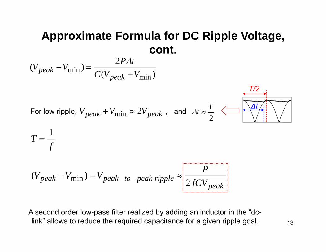
Approximate Formula for DC Ripple Voltage, tcont.
)(2)(
minmin VVC
tPVVpeak
peak
)( minpeak
2VVV For low ripple Ttand∆t
T/2
T 1
,2min peakpeak VVV For low ripple, 2
t and
f
PVVV )(peak
ripplepeaktopeakpeak fCVVVV
2)( min
13
A second order low-pass filter realized by adding an inductor in the “dc-link” allows to reduce the required capacitance for a given ripple goal.

Additional waveforms detailsdd t o a a e o s deta s
• The output voltage frequency is twice that of the input voltage.
O t t lt i l i ll i di t d t ( ll 5%) f th• Output voltage ripple is usually indicated as a percentage (usually < 5%) of the peak input voltage.
14
Output voltage ripple
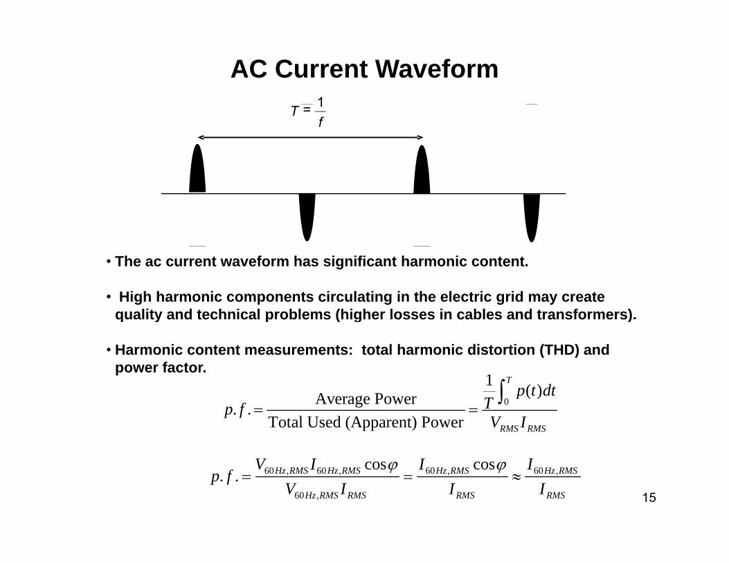
AC Current Waveform1f
T 1=
• The ac current waveform has significant harmonic content.
• High harmonic components circulating in the electric grid may create quality and technical problems (higher losses in cables and transformers)quality and technical problems (higher losses in cables and transformers).
• Harmonic content measurements: total harmonic distortion (THD) and power factor.
1 ( )T
t dt0 ( )Average Power. .Total Used (Apparent) Power RMS RMS
p t dtTp fV I
V I I I
15
60 , 60 , 60 , 60 ,
60 ,
cos cos. . Hz RMS Hz RMS Hz RMS Hz RMS
Hz RMS RMS RMS RMS
V I I Ip f
V I I I

AC Current Waveform• The ac current waveform can be approximated to triangular pulses• The ac current waveform can be approximated to triangular pulses
2i rmsI
16
,2
21,
i rmsi
rms
THDI

“Vampire” Loads
?= ?• “Vampire” loads have high leakage currents and low power factor.
Your new lab safety tool:
17

Estimated Diode Conduction Losses
Estimate the average value I avg of the ac current over the conduction interval T cond
Estimate the average value Vavgof diode forward voltage drop over one conduction i t l T
i(t)
Tcond
interval Tcond
Since the forward voltage on the diode is approximately constant during the conduction
v(t)
condavgavgcondavgavg
avg TIVTIV
P 2404
Watts.
interval, the energy absorbed by the diode during the conduction interval is approximately V avg • I avg • T cond . Each diode has one conduction interval per 60Hz period, so the average power absorbed by all four diodes is then
condavgavgHz
avg T60
18

Forward Voltage on One Diode
Zero Conducting Forward voltage on one diode
Zoom-InForward voltage on one diodeZero one diode
19
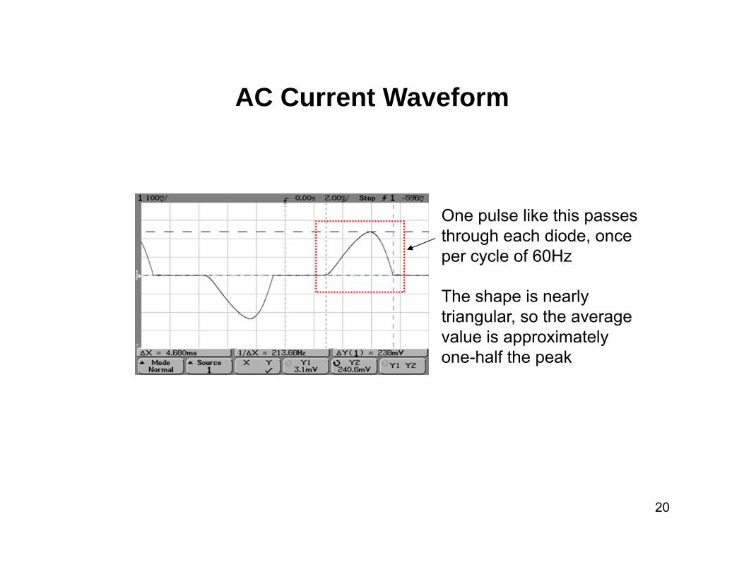
AC Current WaveformC Cu e t a e o
One pulse like this passes through each diode, once
l f 60Hper cycle of 60Hz
The shape is nearly triangular, so the average g , gvalue is approximately one-half the peak
20

Single-phase controlled rectifier
• Goal: to control the dc output voltage component. This objective is achieved by controlling the firing angle of SCRs.
21 T V V
0 0
21 ( ) sin( ) cos( )2 / 2
RT p pdc R
R
V VV v t dt d
T

Three-phase half-wave rectifier
• Assume a balanced three-phase system:

Three-phase half-wave rectifier
• The output voltage ripple frequency is three times that of the input voltage waveforms.
• With diodes:5 / 6, , ,
0 / 6
3 3 31 3( ) sin( ) 22 / 3 2 2 2
RT p L n p L n p L ndc R
R
V V VV v t dt d
T
•With SCRs: ,
0
3 31 ( ) cos( )2
RT p L ndc R
R
VV v t dt
T

Three-phase bridge rectifier
• Still, assume a balanced three-phase system:
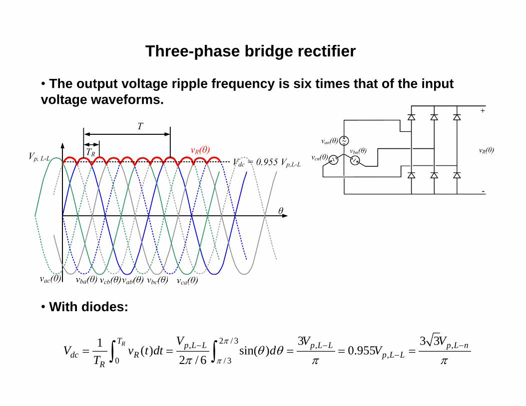
Three-phase bridge rectifier
• The output voltage ripple frequency is six times that of the input voltage waveforms.
• With diodes:
2 / 3, , ,,
0 / 3
3 3 31 ( ) sin( ) 0.9552 / 6
RT p L L p L L p L ndc R p L L
R
V V VV v t dt d V
T
Top Related