


Languages
Pages
Legal


Using IPC/JEDEC-9704 & 9702
Standards for Strain Gage Testing
of Your Printed Wiring Boards
Swapnil Padhye
National Instruments

Agenda
Problem Statement
Solution
How to Implement a Strain Gage Test
Strain Gage Tests at National Instruments
Conclusion
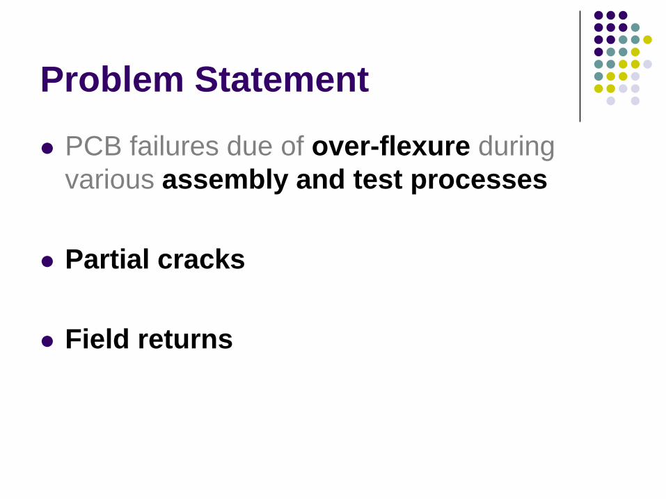
Problem Statement
PCB failures due of over-flexure during
various assembly and test processes
Partial cracks
Field returns
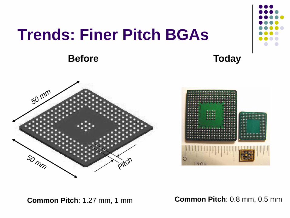
Trends: Finer Pitch BGAs
Common Pitch: 1.27 mm, 1 mm Common Pitch: 0.8 mm, 0.5 mm
Before Today
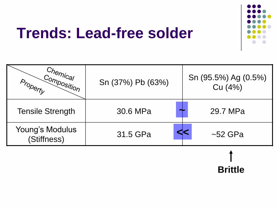
Trends: Lead-free solder
Sn (37%) Pb (63%)Sn (95.5%) Ag (0.5%)
Cu (4%)
Tensile Strength 30.6 MPa 29.7 MPa
Young’s Modulus
(Stiffness)31.5 GPa ~52 GPa
~
<<
Brittle

Trends: PCB Thickness
Year
Co
mm
on
PC
B t
hic
kn
es
s (
Mil)
125
85
45
5
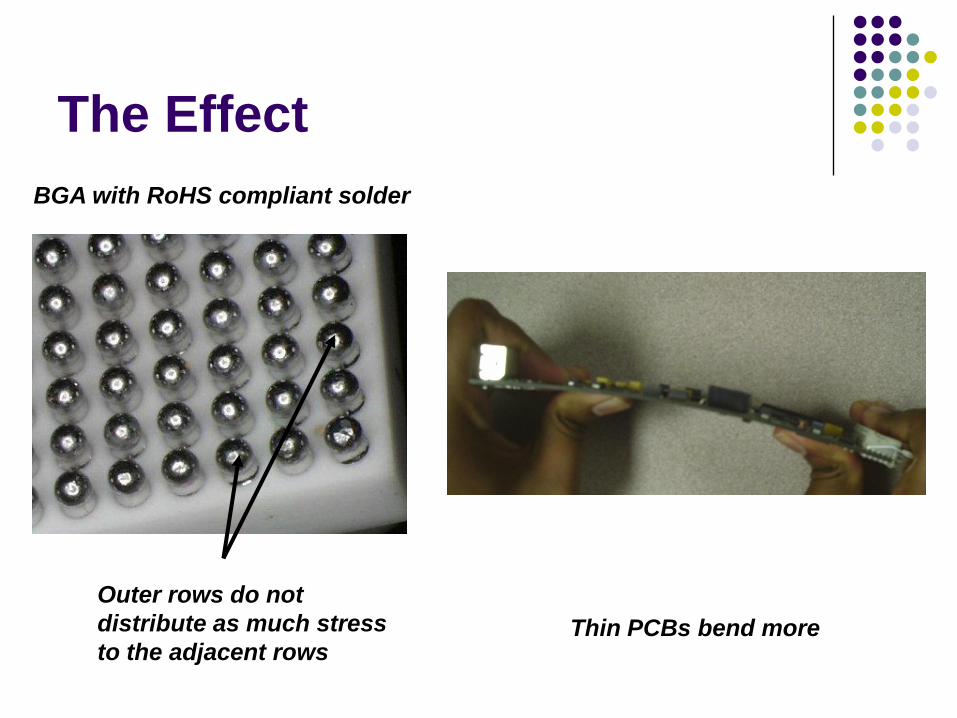
The Effect
Outer rows do not
distribute as much stress
to the adjacent rowsThin PCBs bend more
BGA with RoHS compliant solder

Solution: Strain Gage Testing (SGT)
Identify and correct problem
processes
Assembly
Test
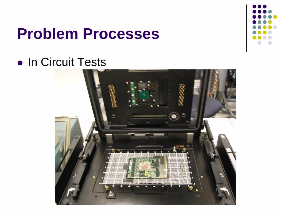
Problem Processes
In Circuit Tests
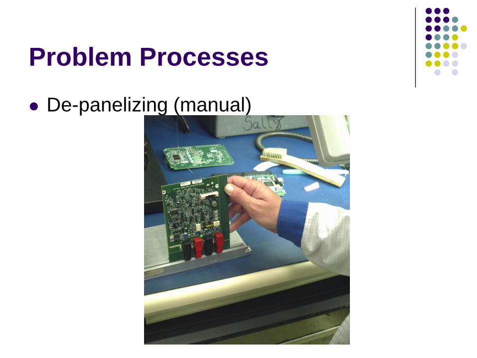
Problem Processes
De-panelizing (manual)

Problem Processes
Edge cutting machines
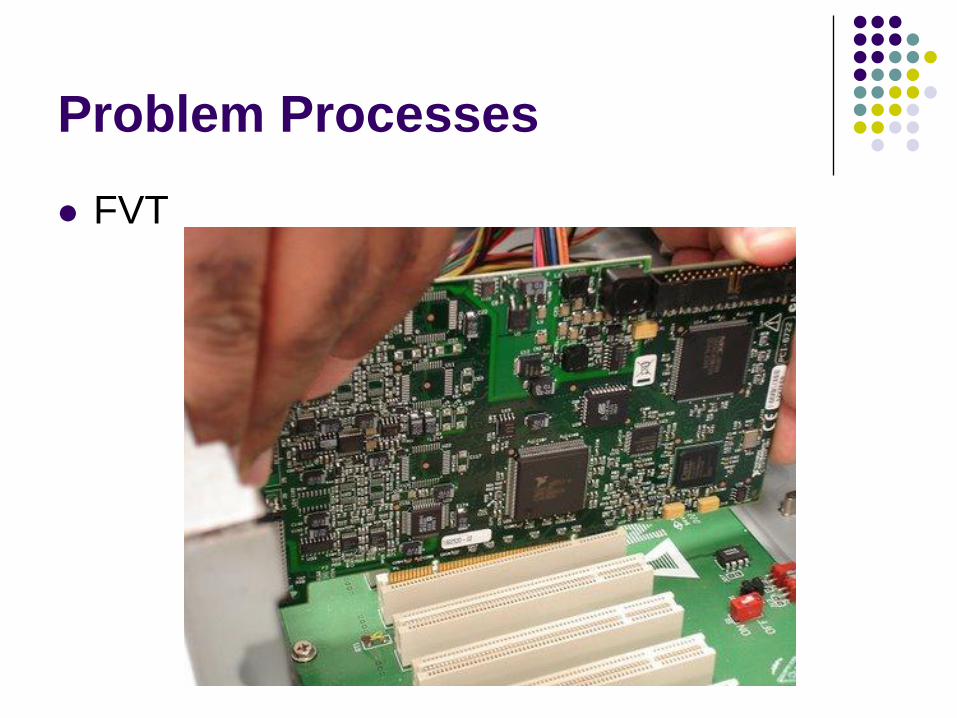
Problem Processes
FVT

Solution: Strain Gage Testing (SGT)
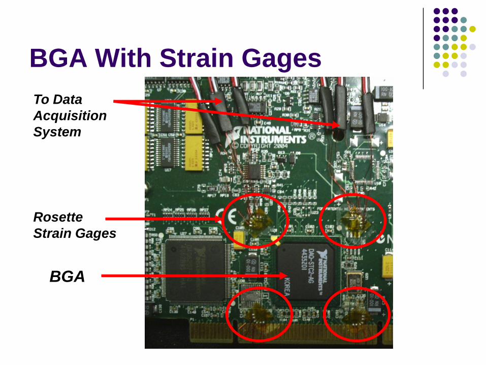
BGA With Strain Gages
BGA
To Data
Acquisition
System
Rosette
Strain Gages
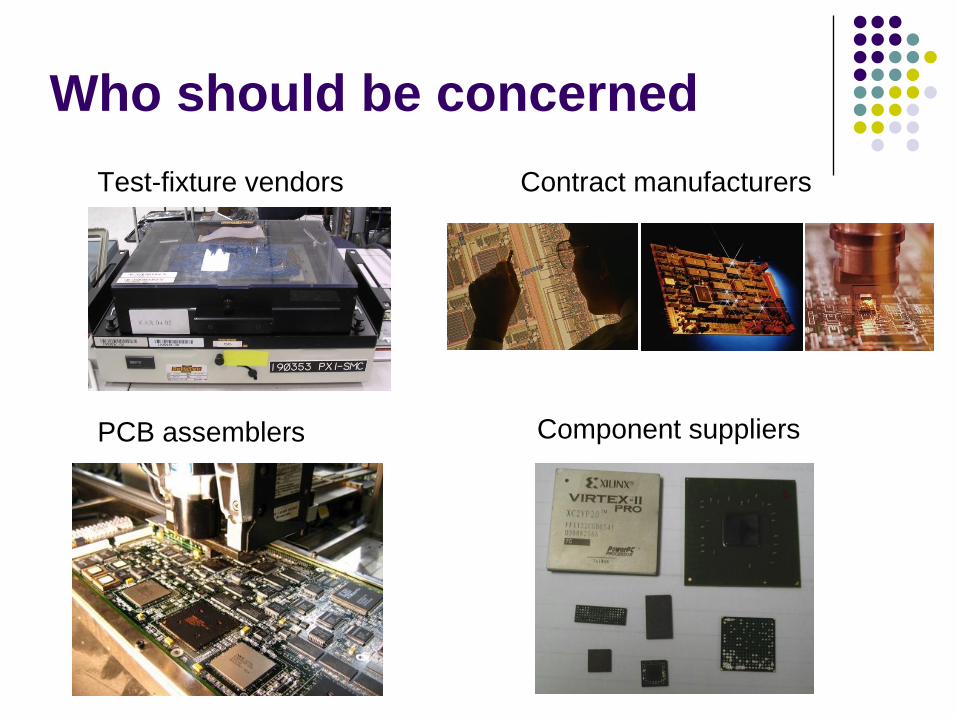
Who should be concerned
Test-fixture vendors Contract manufacturers
PCB assemblers Component suppliers
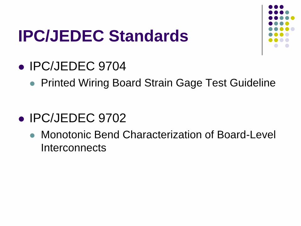
IPC/JEDEC Standards
IPC/JEDEC 9704
Printed Wiring Board Strain Gage Test Guideline
IPC/JEDEC 9702
Monotonic Bend Characterization of Board-Level
Interconnects
Industry involvement
Intel
Cisco Systems
Sun Microsystems
Solectron
Circuit Check
….
IPC/JEDEC 9704
Recommended strain gages
Gage placement and attachment
Measurement equipment
Data analysis
Reporting Template

SGT System I/O Requirements
Hardware
Sampling rate of 2KHz
At least 3 channels (12 or more recommended)
Simultaneous sampling of all channels
12 to 16 bit input resolution
Low-pass filter
Gain
Software
User Interface
Reporting

Components of a SGT
Sensor
Rosette strain
gages
Signal
Conditioning
Data Acquisition
Software
Reporting
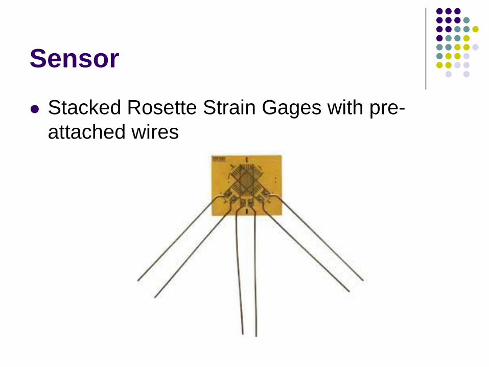
Sensor
Stacked Rosette Strain Gages with pre-
attached wires
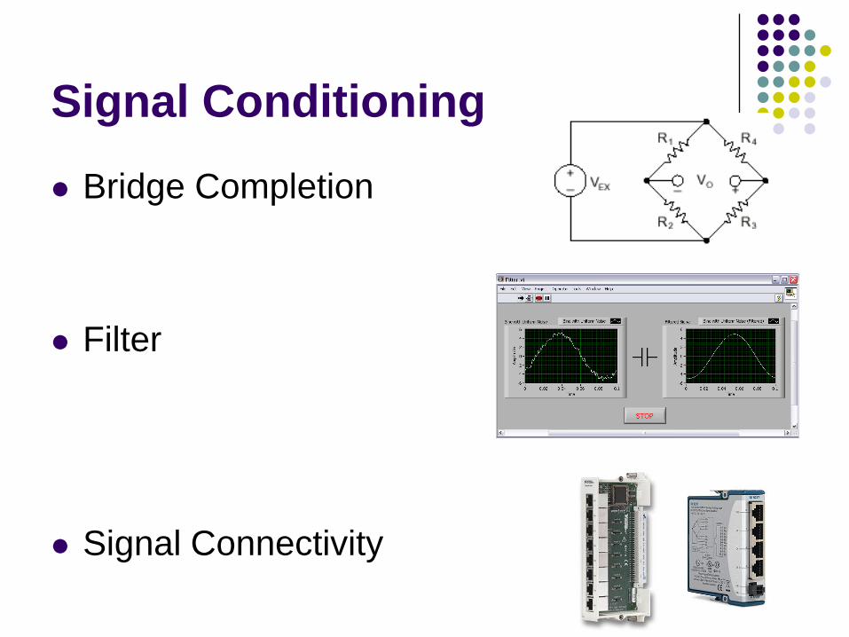
Signal Conditioning
Bridge Completion
Filter
Signal Connectivity

Data Acquisition
Sampling Rate
Number of Channels
Simultaneous Sampling
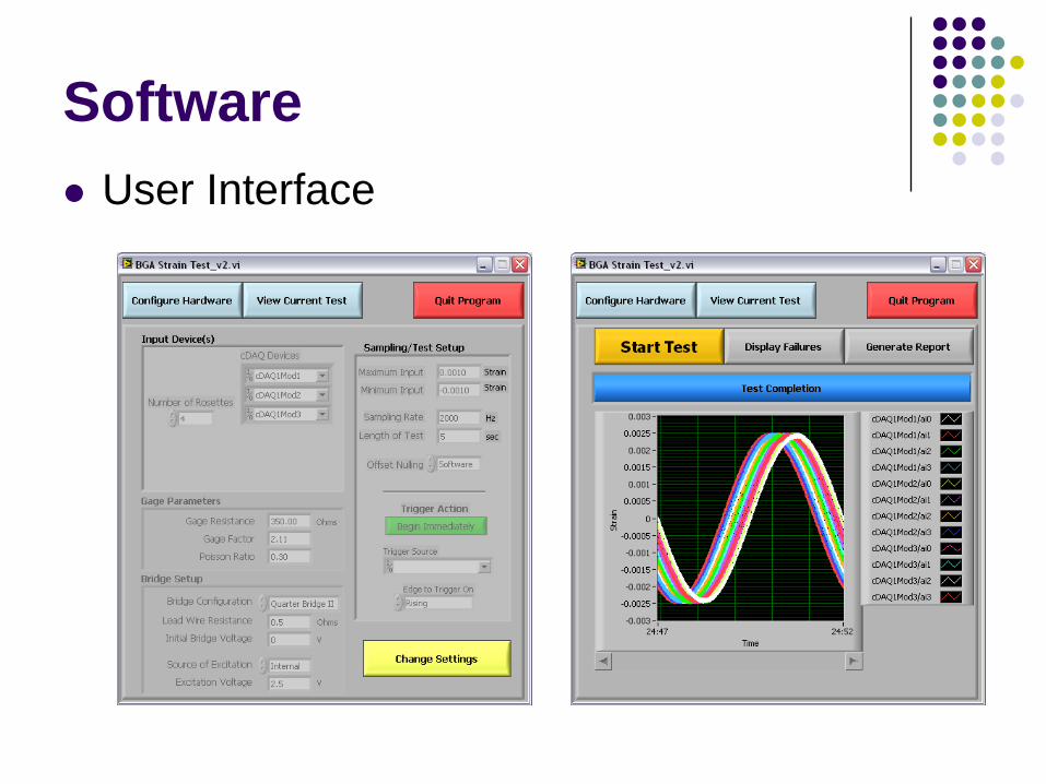
Software
User Interface
Software
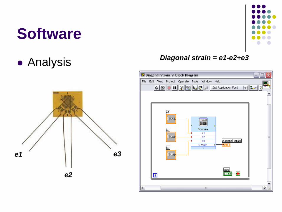
AnalysisDiagonal strain = e1-e2+e3
e1
e2
e3
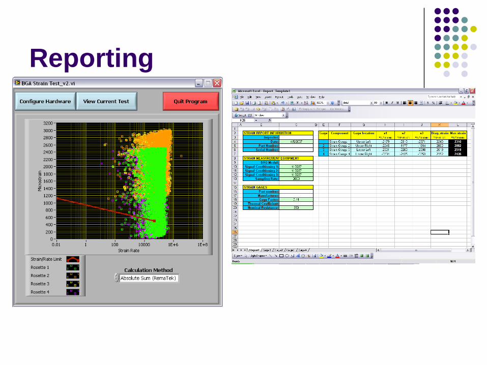
Reporting

Results at National Instruments:
Effectively use Strain Gage Testing for
correcting ICT fixtures
Virtual Instrumentation solution
Flexible Software
Modular Hardware
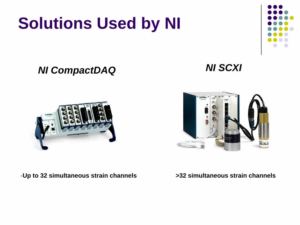
Solutions Used by NI
NI CompactDAQ
>32 simultaneous strain channels-Up to 32 simultaneous strain channels
NI SCXI

Conclusion
Critical to be Lead-free and RoHS compliant
Adoption of strain gage testing for better PCB
assembly yields
Top Related