


Languages
Pages
Legal


Slide 1
Printed Circuit BoardPrinted Circuit Board
Design, Development and Fabrication ProcessDesign, Development and Fabrication Process
This presentation is courtesy of PCB3D.COM
Steve RosePrinted Circuit Board Design Engineer

Slide 2
IntroductionIntroductionIntroduction
This presentation outlines the printed circuit board design process, and the details required to capture design intent.
These guidelines were created to ensure an error-free robust design that will meet or exceed cost expectations, satisfy fabrication, assembly and test criteria, and conform to form, fit and function requirements.
1
PCB3D.com
PCB 101

Slide 3
Design Process OverviewDesign Process OverviewDesign Process Overview
? Concept? Electrical Architect? Electrical Component Selection? Schematic ? Bill of Materials? PCB Library Component Development? Netlist? PCB Netlist Verification? Mechanical Inputs? Design Requirements? PCB Design? PCB Design Verification? Gerber File Generation? PCB DFT / DFM? Design Review (Preliminary)? Incorporate Design Review and DFT/ DFM Feedback? Overlay Output? Gerber Analysis and Plotfile Verification? Panelize PCB? Finalize Gerber Fabrication Package? PCB Fabrication
2
PCB3D.com
Slide 4
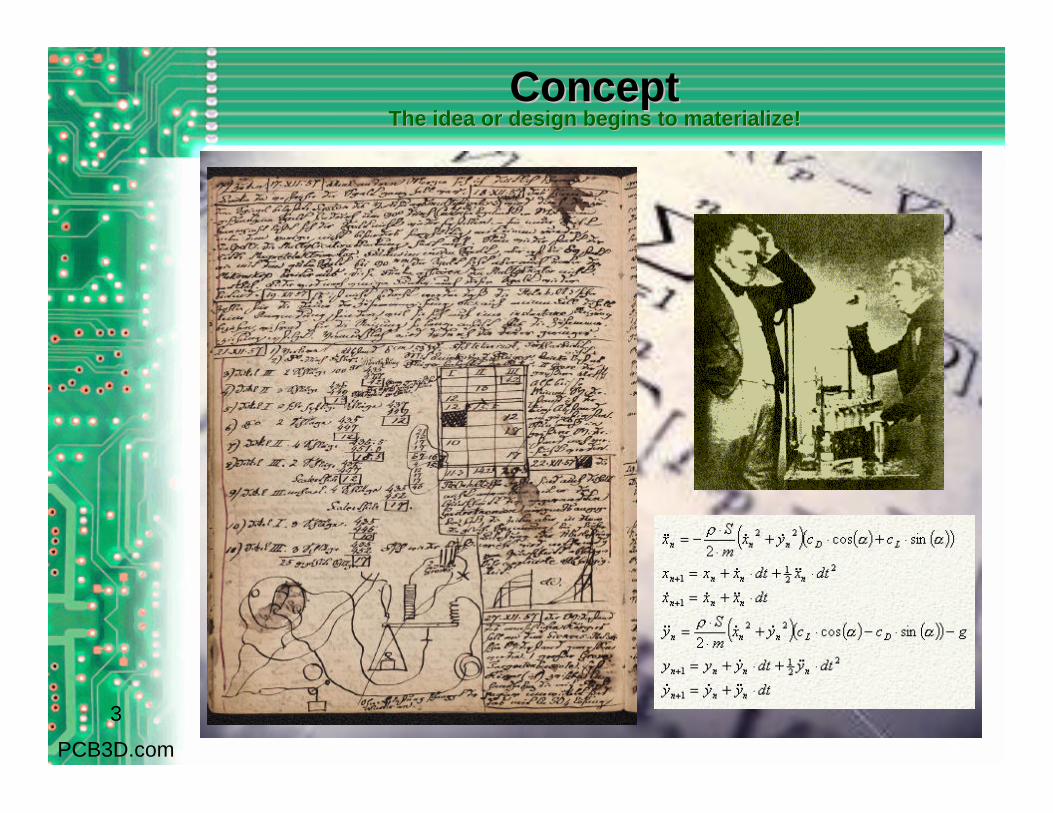
ConceptConceptThe idea or design begins to materialize!The idea or design begins to materialize!
3
PCB3D.com
Slide 5
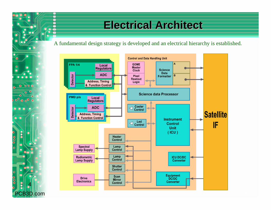
Electrical ArchitectElectrical Architect
4
PCB3D.com
A fundamental design strategy is developed and an electrical hierarchy is established.
Slide 6
Electrical Component SelectionElectrical Component Selection
5
PCB3D.com
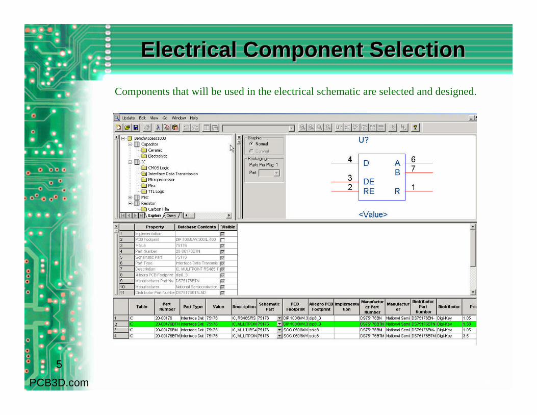
Components that will be used in the electrical schematic are selected and designed.

Slide 7
SchematicSchematic
6
PCB3D.com
The electrical components are placed in the schematic and net connections established.

Slide 8
Bill of Materials
7
PCB3D.com
The Bill of Materials is derived from the components that exist in the schematic.
Slide 9
PCB Component DevelopmentPCB Component Development
8
PCB3D.com
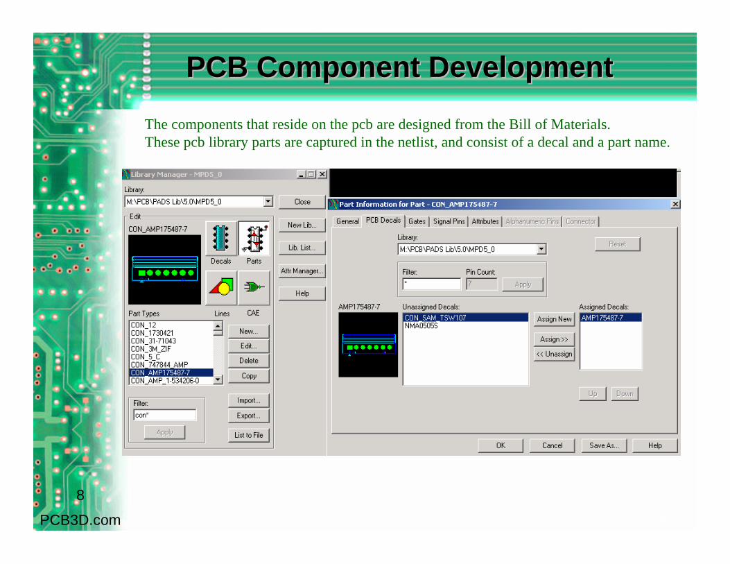
The components that reside on the pcb are designed from the Bill of Materials. These pcb library parts are captured in the netlist, and consist of a decal and a part name.

Slide 10
NetlistNetlist
9
PCB3D.com
The netlist is typically an ASCII format generated from the schematic. It contains all components (*part*) and connections (*net*) required for the pcb design.
Slide 11
PCB Netlist VerificationPCB Netlist Verification
10
PCB3D.com
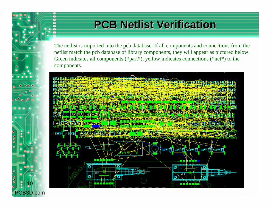
The netlist is imported into the pcb database. If all components and connections from the netlist match the pcb database of library components, they will appear as pictured below. Green indicates all components (*part*), yellow indicates connections (*net*) to the components.

Slide 12
Mechanical InputsMechanical Inputs
11
PCB3D.com
Mechanical placement strategies are imported into the pcb database in the form of a DXF.

Slide 13
PCB Design RequirementsPCB Design Requirements
? Customer Specification? Electrical Requirements? Mechanical Requirements? Optical or Data Requirements? IPC Requirements? Packaging Requirements? UL, IEEE, Belcore, Telcordia
12
PCB3D.com
The following requirements and specifications are established prior to pcb layout.
Slide 14
PCB Design ElementsPCB Design ElementsPCB Design Elements
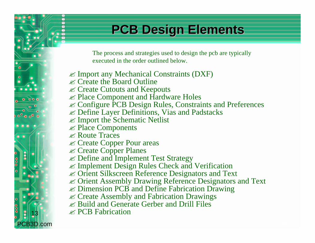
? Import any Mechanical Constraints (DXF) ? Create the Board Outline? Create Cutouts and Keepouts? Place Component and Hardware Holes ? Configure PCB Design Rules, Constraints and Preferences?Define Layer Definitions, Vias and Padstacks? Import the Schematic Netlist? Place Components? Route Traces? Create Copper Pour areas? Create Copper Planes?Define and Implement Test Strategy? Implement Design Rules Check and Verification?Orient Silkscreen Reference Designators and Text?Orient Assembly Drawing Reference Designators and Text?Dimension PCB and Define Fabrication Drawing? Create Assembly and Fabrication Drawings? Build and Generate Gerber and Drill Files? PCB Fabrication13
PCB3D.com
The process and strategies used to design the pcb are typically executed in the order outlined below.
Slide 15
PCB Design: KeepoutsPCB Design: Keepouts
14
PCB3D.com
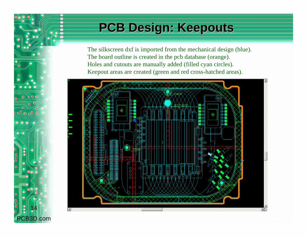
The silkscreen dxf is imported from the mechanical design (blue).The board outline is created in the pcb database (orange). Holes and cutouts are manually added (filled cyan circles). Keepout areas are created (green and red cross-hatched areas).
Slide 16
PCB Design: ComponentsPCB Design: Components
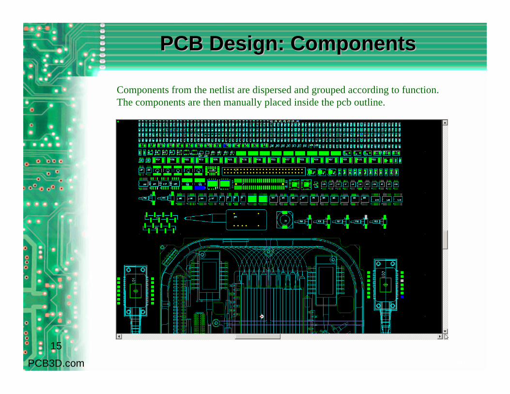
Components from the netlist are dispersed and grouped according to function.The components are then manually placed inside the pcb outline.
15
PCB3D.com
Slide 17
PCB Design: PlacementPCB Design: Placement
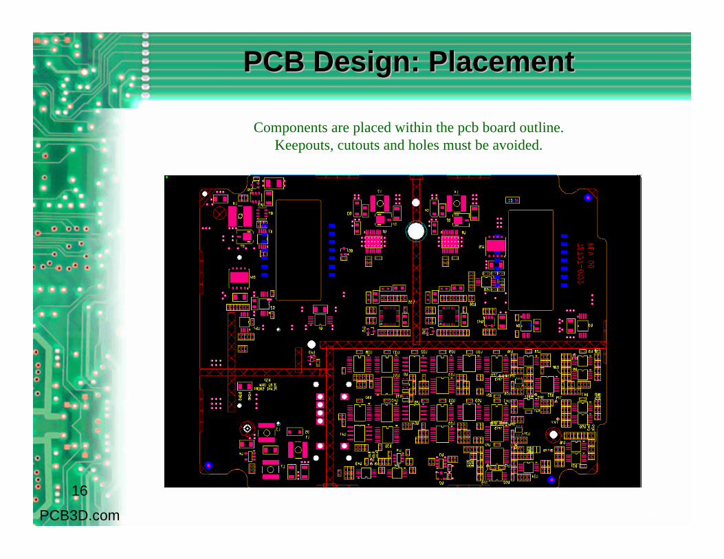
Components are placed within the pcb board outline.Keepouts, cutouts and holes must be avoided.
16
PCB3D.com
Slide 18
PCB Design: RoutingPCB Design: Routing
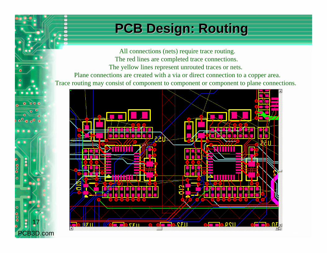
All connections (nets) require trace routing.The red lines are completed trace connections.
The yellow lines represent unrouted traces or nets. Plane connections are created with a via or direct connection to a copper area.
Trace routing may consist of component to component or component to plane connections.
17
PCB3D.com
Slide 19
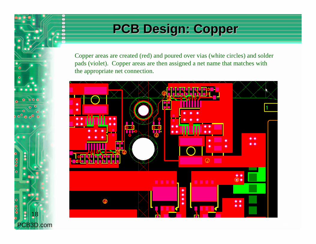
PCB Design: CopperPCB Design: Copper
Copper areas are created (red) and poured over vias (white circles) and solder pads (violet). Copper areas are then assigned a net name that matches with the appropriate net connection.
18
PCB3D.com

Slide 20
PCB Design: PlanePCB Design: Plane
DIGITAL GND
ANALOG GND
The copper planes are created, split and defined according to the design rules and net requirements for each layer. Thermal and non-thermal connections are placed accordingly.
19
PCB3D.com

Slide 21
PCB Design: DFTPCB Design: DFT
Design for Test involves placement of test points into the completed pcb.Two types of test points are used. Flying Probe (FPT) and In Circuit (ICT).DFT analysis is executed and test points are audited for compliance and testability.
20
PCB3D.com
Slide 22
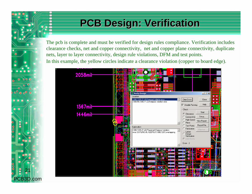
PCB Design: VerificationPCB Design: Verification
The pcb is complete and must be verified for design rules compliance. Verification includes clearance checks, net and copper connectivity, net and copper plane connectivity, duplicate nets, layer to layer connectivity, design rule violations, DFM and test points.In this example, the yellow circles indicate a clearance violation (copper to board edge).
21
PCB3D.com

Slide 23
Gerber FilesGerber Files
Typical Gerber File Structure
– Electrical Design Layers – Silkscreen– Solder Mask– Solder Paste– Fabrication Drawings– Assembly Drawings– Aperture Files– Drill Files– Netlist – X-Y Placement Data
Gerber files are created to enable plotting of the individual design file elements.Depending on their function, each Gerber file is compiled as an individual electrical layer, process or design reference.
22
PCB3D.com

Slide 24
Gerber FilesGerber Files
This is a typical Gerber file design menu. From this menu, design data can be manipulated to any number of conditions to achieve the desired results.
23
PCB3D.com

Slide 25
Gerber Files: Electrical LayersGerber Files: Electrical Layers
These Gerber files are processed to create each electrical layer (internal and external) that will ultimately be finished in copper on the pcb.
24
PCB3D.com
Slide 26
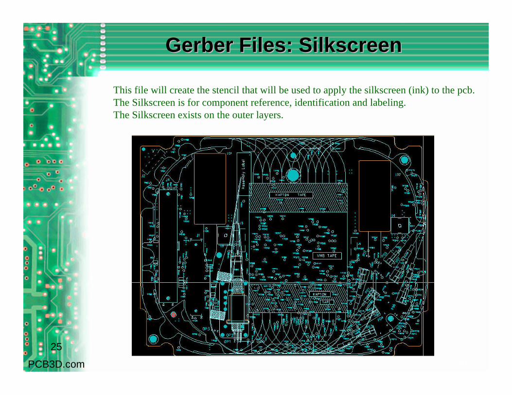
Gerber Files: SilkscreenGerber Files: Silkscreen
This file will create the stencil that will be used to apply the silkscreen (ink) to the pcb.The Silkscreen is for component reference, identification and labeling. The Silkscreen exists on the outer layers.
25
PCB3D.com
Slide 27
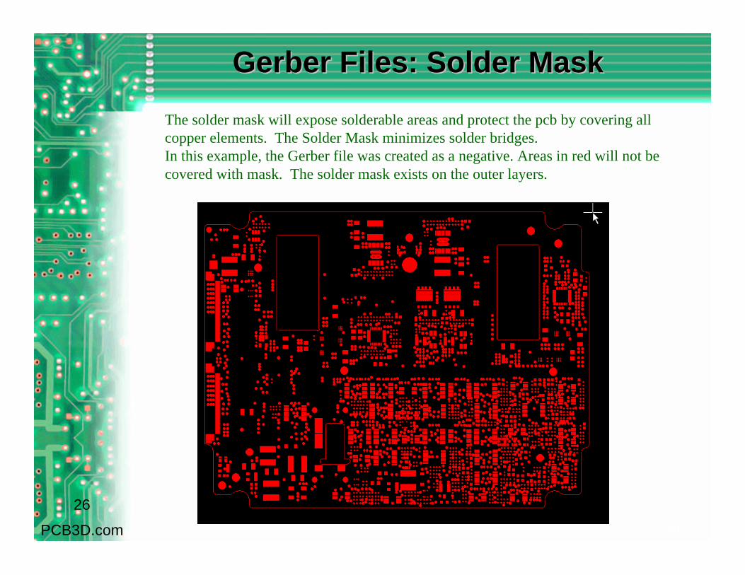
Gerber Files: Solder MaskGerber Files: Solder Mask
The solder mask will expose solderable areas and protect the pcb by covering all copper elements. The Solder Mask minimizes solder bridges.In this example, the Gerber file was created as a negative. Areas in red will not be covered with mask. The solder mask exists on the outer layers.
26
PCB3D.com

Slide 28
Gerber Files: Solder PasteGerber Files: Solder Paste
This file will be used to create a solder paste stencil. Prior to the board assembly, the stencil will be used to apply solder paste directly to the pads on the pcb (areas in yellow). Once the solder paste is applied, surface mount components can be placed and soldered.
27
PCB3D.com

Slide 29
Gerber Files: Fabrication DrawingGerber Files: Fabrication Drawing
This file will be created to display all mechanical and fabrication design parameters of the pcb. Parameters include layer stackup, board thickness, tolerance, drill file, copper weight, dimensioning, and applicable design standards .
28
PCB3D.com

Slide 30
Gerber Files: Fabrication DetailsGerber Files: Fabrication Details
29
PCB3D.com
Pcb manufacturing details include drill size, plating, drill location information, electrical layer stackup, board thickness, slots, cutouts and tolerance.

Slide 31
Gerber Files: Assembly DrawingGerber Files: Assembly Drawing
30
PCB3D.com
Identifies location and orientation of the electronic components to be placed.
Slide 32
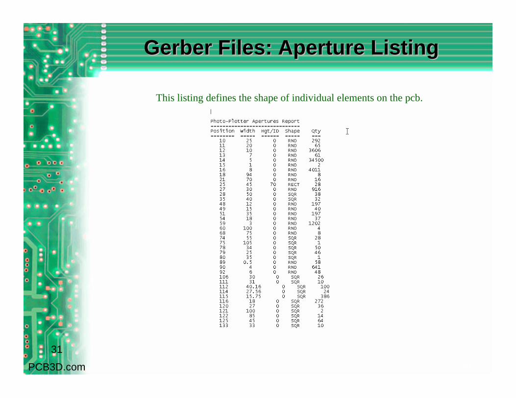
Gerber Files: Aperture ListingGerber Files: Aperture Listing
31
PCB3D.com
This listing defines the shape of individual elements on the pcb.
Slide 33
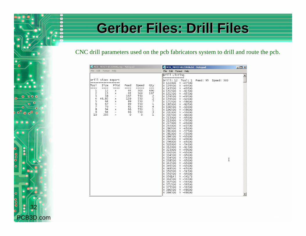
Gerber Files: Drill FilesGerber Files: Drill Files
32
PCB3D.com
CNC drill parameters used on the pcb fabricators system to drill and route the pcb.
Slide 34
Design Review Process: DFT/DFMDesign Review Process: DFT/DFM
? The Preliminary PCB Design is presented and scrutinized by Manufacturing, Test, Reliability, Electronics and Mechanical Engineering.
? DFM/DFT feedback is reviewed and validated.? Design Guidelines are reviewed and verified.? Cost considerations are addressed.? Manufacturing and assembly process are reviewed.? A final PCB Design review will present all actions from the
Preliminary Design Review.? Gerber files are analyzed and design intent validated.? Mechanical and PCB files are overlaid and verified.? Gerber data files are created.? The PCB Design is released.
33
PCB3D.com
(Preliminary and Final Design Review Audit)
Slide 35
PCB DFT / DFM: AnalysisPCB DFT / DFM: Analysis
34
PCB3D.com
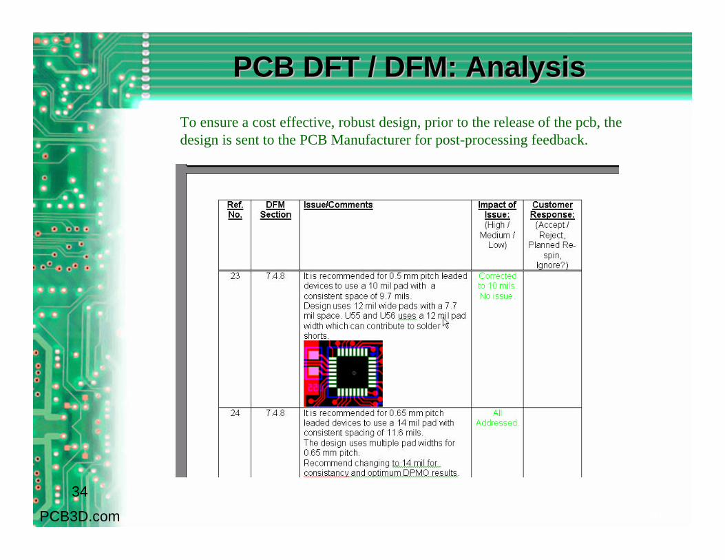
To ensure a cost effective, robust design, prior to the release of the pcb, the design is sent to the PCB Manufacturer for post-processing feedback.

Slide 36
Design Review ProcessDesign Review Process
Interface Board PCBA Final Design Review.Attendees: Lori Karl, Steve Rose, Scott Stewart, Lloyd Newfield, John Lodge, Jim
McLaren, Jody Baron1. Confirm final mechanical overlay check with Jody. (Complete)2. VOA requirements have been removed. (Complete)3. Scott to contact Fab house regarding modified soldermask opening on 9pin BGA.
(Complete)
Interface Board PCBA Preliminary Design ReviewAttendees: Rich Riddle, Jim McLaren, Scott Stewart, John Mansfield, Steve Rose,
Lloyd Newfield, Jody Baron 1. Lloyd to provide part numbers to Rich on EDVT parts which are planned to be
NOPOP'ed at assembly, but need to be installed for EDVT testing by Rich's group. Lloyd to provide part numbers and target quantity to Rich.
2. Jody will lower ribs on new base under J7 (flex connector) to prevent shorting base to pads or vias. Rib to be removed under J6. Middle rib will be lowered .040”, to clear pads of J7.
35
PCB3D.com
(Final Review) Incorporate Design Review Notes and DFT/ DFM Feedback.
Slide 37
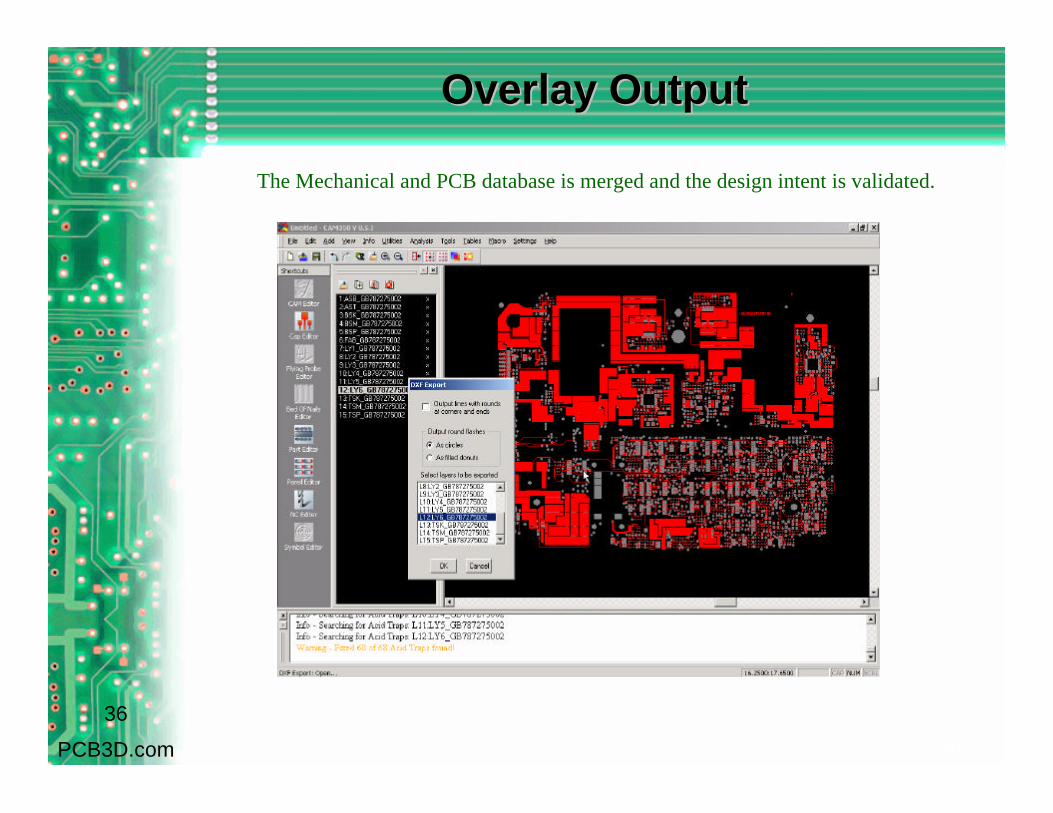
Overlay OutputOverlay Output
36
PCB3D.com
The Mechanical and PCB database is merged and the design intent is validated.
Slide 38
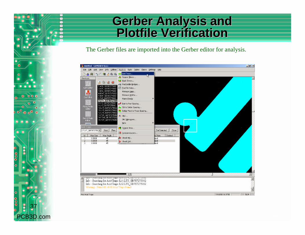
Gerber Analysis and Gerber Analysis and PlotfilePlotfile VerificationVerification
37
PCB3D.com
The Gerber files are imported into the Gerber editor for analysis.

Slide 39
PCB DFT / DFM: PCB DFT / DFM: PanelizationPanelization
38
PCB3D.com
To facilitate electronic assembly, a panel is created around around the pcb.
Slide 40
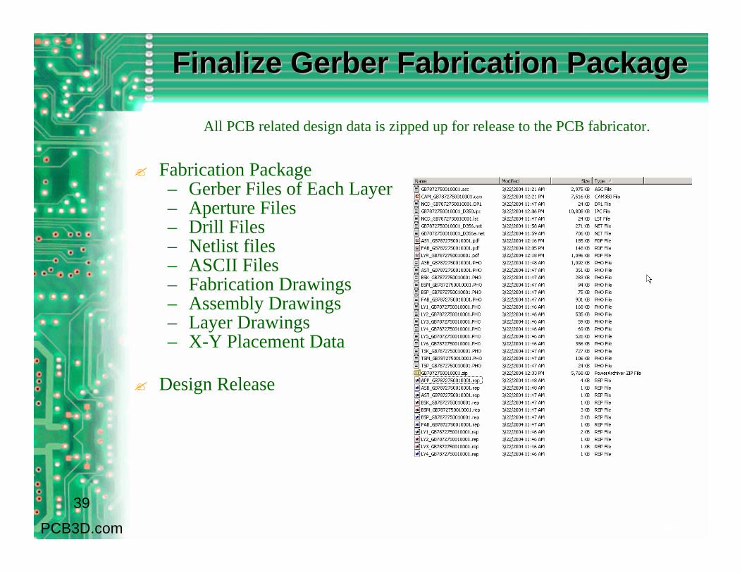
Finalize Gerber Fabrication PackageFinalize Gerber Fabrication PackageFinalize Gerber Fabrication Package
? Fabrication Package– Gerber Files of Each Layer– Aperture Files– Drill Files– Netlist files– ASCII Files– Fabrication Drawings– Assembly Drawings– Layer Drawings– X-Y Placement Data
? Design Release
39
PCB3D.com
All PCB related design data is zipped up for release to the PCB fabricator.
Slide 41
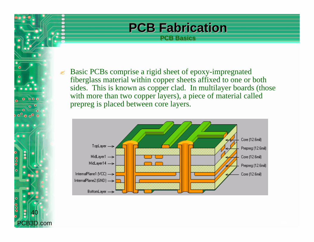
PCB FabricationPCB Basics
PCB FabricationPCB FabricationPCB BasicsPCB Basics
? Basic PCBs comprise a rigid sheet of epoxy-impregnated fiberglass material within copper sheets affixed to one or both sides. This is known as copper clad. In multilayer boards (those with more than two copper layers), a piece of material called prepreg is placed between core layers.
40
PCB3D.com
Slide 42
PCB FabricationPCB Basics (continued)
PCB FabricationPCB FabricationPCB Basics (continued)PCB Basics (continued)
? The outer copper surface of the PCB must be processed to form circuit paths, or traces, that make the connections between components. Analogous to wires, the traces are formed using a photolithographic process. In that process, the copper layers are treated with chemical etching that removes unneeded portions of the copper, leaving only the traces and pads required for component soldering.
? Pads can be fabricated in many shapes and formats. Components are typically attached to these pads as surface mount, through hole, or both. After photolithography is completed, the board is drilled and through holes are plated.
41
PCB3D.com

Slide 43
For multi-layer designs, the first step is to print etch the inner layers.Each inner circuit is transferred to the copper panel using photographic dry film. The film is hot-roll laminated onto the copper panel. The film tooling is exposed onto the panel typically using a 5-kilo Watt light source. The panels are put through a series of vertical conveyors containing various wet processing chemicals. First, the exposed film on the panels is developed, then the exposed copper(no film on it) is etched away and finally the remaining film isstripped off resulting in bare copper circuits on laminate. Thisprocess usually takes about three hours.
The inner layers are then pinned in a stack with thin sheets of epoxy glass pre-preg which separates the copper layers. The outer layers are made with a foil of copper. The stack is pinned between two heavy metal plates creating a "book." This book is put in a hydraulic/heated press for about two hours at 350 degrees F. Thehydraulic pressure is approximately three tons.
PCB FabricationProcess
PCB FabricationPCB FabricationProcessProcess
42
PCB3D.com
Slide 44
PCB FabricationProcess (continued)
PCB FabricationPCB FabricationProcess (continued)Process (continued)
Once pressed, these panels look just like double sided laminate and are ready for drilling. For double-sided panels, drilling is the first process. The panels are pinned to the table of a CNC drill. The drill program is loaded, and the proper drill bit sizes are loaded into the auto-tool-change holders. A typical load size is 15 panels up. The panels are then deburredafter drilling. This process usually lasts anywhere from 30 minutes to two hours.
Electroless copper is next. In order to put a thin (0.000025") coat of copper inside the drilled holes, there is a series of chemicals required to condition, clean, and activate the surface inside the holes. The panels sit in a blue liquid of suspended copper for about 45 minutes; the entire process takes about two hours.
Primary image (i.e., the top & bottom layers) is applied using dry film plating resist, as before with the inner layers. It is developed, and then it goes into a copper plating procedure. The panels are cleaned andactivated chemically, then connected to a rack inside a large volume of copper solution.
43
PCB3D.com

Slide 45
PCB FabricationProcess (continued)
PCB FabricationPCB FabricationProcess (continued)Process (continued)
At 25 amps/square foot of copper, the panels are electro-plated for about one hour to achieve one ounce of copper in the holes and on the surface. Next, tin is plated on top of the copper. (During the entire time, the dry film (plating resist) is on the panels to prevent plating where there are no circuits.)
After plating, the dry film plating resist is stripped off the panel leaving exposed copper. This copper is chemically etched off thepanel leaving only the tin over copper circuitry. Next, the tin is stripped from the panel leaving bare copper circuits.
Solder Mask is applied directly over the bare copper. Liquid Photo Imagable (LPI) Solder Mask is flooded onto the panel using a screen. It is then tack dried in a convection oven. The panel isaligned to the Solder Mask tooling film using registration pins and then exposed in a 5 kW light source for about 20 seconds. The panel is then developed to remove LPI Solder Mask from the pads and holes. Finally, the panel is baked to cure the remaining mask to its permanent state. The total LPI time is about two hours.
44
PCB3D.com
Slide 46
PCB FabricationProcess (continued)
PCB FabricationPCB FabricationProcess (continued)Process (continued)
Legend ink (silkscreen) is screened onto the panel using a screen stencil, which is photographically made from the Legend film work. The panel is cured in a convection oven to complete the screening process in about an hour.
Next, the panel is put through a Hot Air Solder Leveler (HASL) in order to put solder on the pads and in the holes. It consists of a flux tank, a solder tank at about 360 degrees F, and air knives to blow out the holes.
The CNC routing is the final step to the pcb fabrication process. The panels are pinned to a backup material. The CNC program is loaded into memory, and a router bit is placed in the tool changer. Normally, an 0.093" size bit is used. The parts are routed out individually. Gold fingers, if present, are then beveled.
45
PCB3D.com
END
Top Related