


Languages
Pages
Legal

Cryogenic RF Characterization of Superconducting Materials at SLAC with Cu and Nb-Coated Cavities
Paul B. Welander, Matt Franzi, Jiquan Guo*, Sami Tantawi
SLAC National Accelerator Laboratory, Menlo Park, CA 94025
6 October 2014
* now at JLab
2TFSRF 2014 – P. Welander – [email protected]
Outline
• Motivation
• Review of Previous Work at SLAC
• New Cryostat and New Cavity
• Initial Measurements on Bulk Nb
• Thin Film Growth at Stanford
3TFSRF 2014 – P. Welander – [email protected]
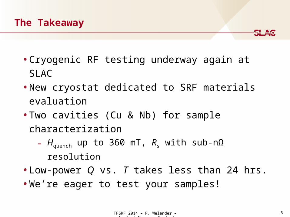
The Takeaway
• Cryogenic RF testing underway again at SLAC
• New cryostat dedicated to SRF materials evaluation
• Two cavities (Cu & Nb) for sample characterization
- Hquench up to 360 mT, Rs with sub-nΩ resolution
• Low-power Q vs. T takes less than 24 hrs.
• We’re eager to test your samples!
TFSRF 2014 – P. Welander – [email protected]
Motivation
Test bed for SRF materials
• Characterize a variety of samples, bulk and thin-film
• Magnetic quenching field measurements up to high fields- Possibly higher than Nb’s 170-180 mT
• Quick testing cycles with small (easy to coat) samples
• Able to explore higher Tc materials (e.g. MgB2, A15s)
• Surface resistance characterization (no longer Cu-limited)
Non-superconducting materials
• RRR of copper in different forms
• Other materials, such as complex oxides
TFSRF 2014 – P. Welander – [email protected]
System Capabilities
• Characterize surface impedance by measuring the quality factor, Q0, of a cavity at 11.4 GHz, down to 4 K
• Capable of low power (PNA) and high power (Klystron) measurements
• Compact design thanks to X-band design (5.5” diameter)• Interchangeable flat cavity bottom, fits 2” diameter samples
up to 0.25” thick.• Cavity design maximizes H-field and minimizes E-field on
the sample surface
• Can achieve Hpeak ~ 360 mT with 50 MW Klystron running 1.6 µs flat pulses and Qe ~ 3.2e5, Q0 ~ 3.2e5
• New Nb-coated cavity designed for Qe ~ 3.2e7, Q0 ~ 3.2e7
6TFSRF 2014 – P. Welander – [email protected]
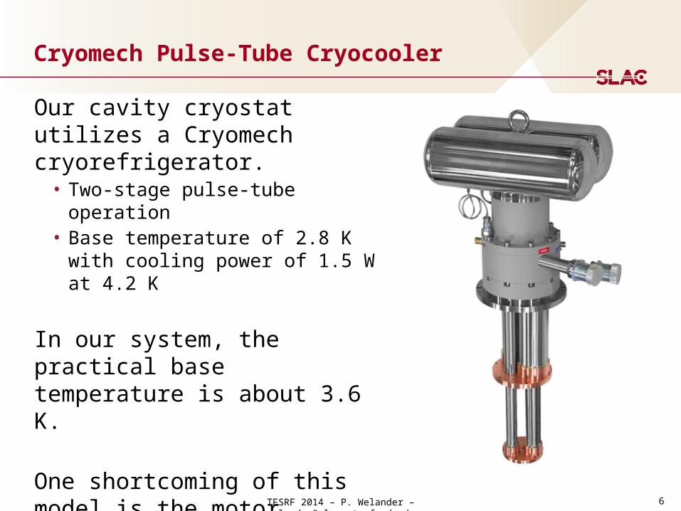
Cryomech Pulse-Tube Cryocooler
Our cavity cryostat utilizes a Cryomech cryorefrigerator.
• Two-stage pulse-tube operation• Base temperature of 2.8 K with
cooling power of 1.5 W at 4.2 K
In our system, the practical base temperature is about 3.6 K.
One shortcoming of this model is the motor vibrations large fluctuations in resonant peak
• Solved in new cryostat by using remote motor version
TFSRF 2014 – P. Welander – [email protected]
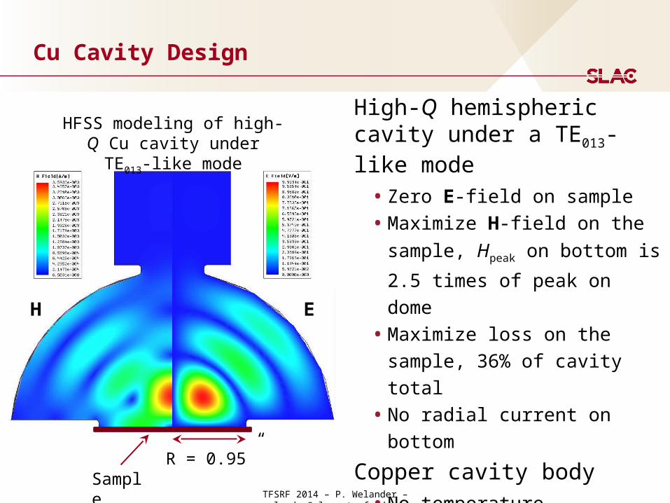
Cu Cavity Design
High-Q hemispheric cavity under a TE013-like mode
• Zero E-field on sample
• Maximize H-field on the sample,
Hpeak on bottom is 2.5 times of
peak on dome
• Maximize loss on the sample,
36% of cavity total
• No radial current on bottom
Copper cavity body• No temperature transition or
quenching
• Higher surface impedance
• Coupling sensitive to iris radius
HFSS modeling of high-Q Cu cavity under TE013-like mode
SampleR = 0.95”
H E
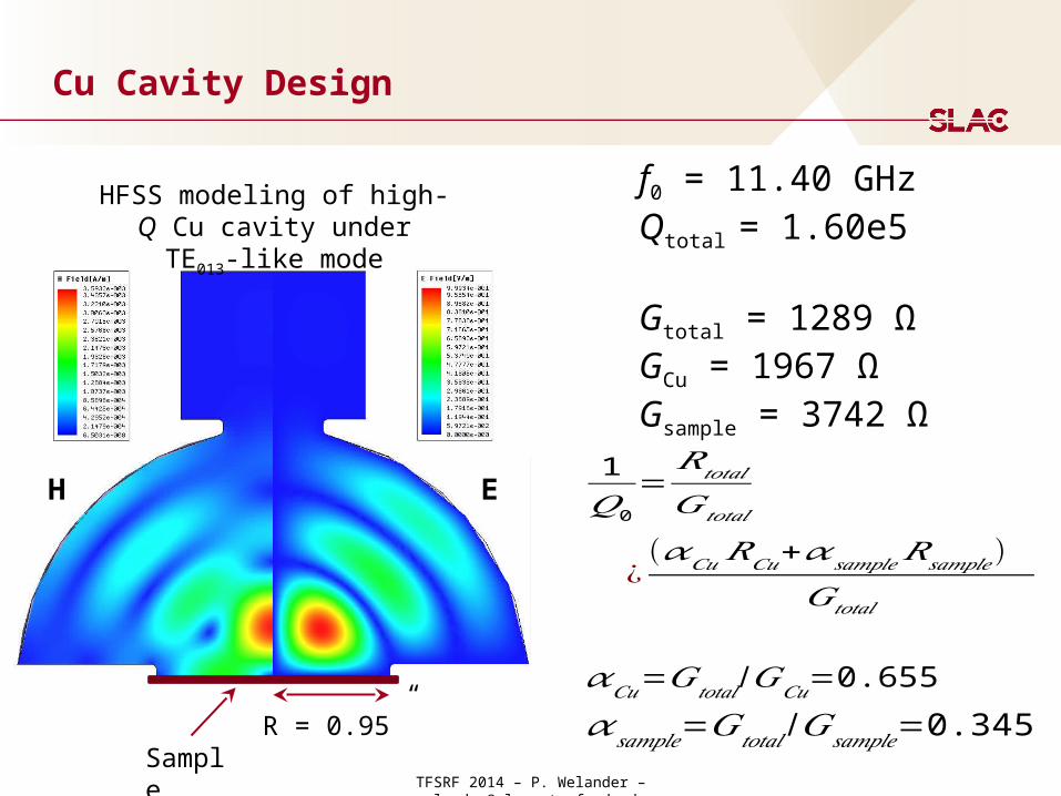
TFSRF 2014 – P. Welander – [email protected]
Cu Cavity Design
HFSS modeling of high-Q Cu cavity under TE013-like mode
SampleR = 0.95”
H E
f0 = 11.40 GHzQtotal = 1.60e5
Gtotal = 1289 ΩGCu = 1967 ΩGsample = 3742 Ω
1𝑄0
=𝑅𝑡𝑜𝑡𝑎𝑙
𝐺𝑡𝑜𝑡𝑎𝑙
¿(𝛼𝐶𝑢𝑅𝐶𝑢+𝛼𝑠𝑎𝑚𝑝𝑙𝑒𝑅𝑠𝑎𝑚𝑝𝑙𝑒)
𝐺𝑡𝑜𝑡𝑎𝑙
𝛼𝑠𝑎𝑚𝑝𝑙𝑒=𝐺𝑡𝑜𝑡𝑎𝑙/𝐺𝑠𝑎𝑚𝑝𝑙𝑒=0.345𝛼𝐶𝑢=𝐺𝑡𝑜𝑡𝑎𝑙 /𝐺𝐶𝑢=0.655
9TFSRF 2014 – P. Welander – [email protected]
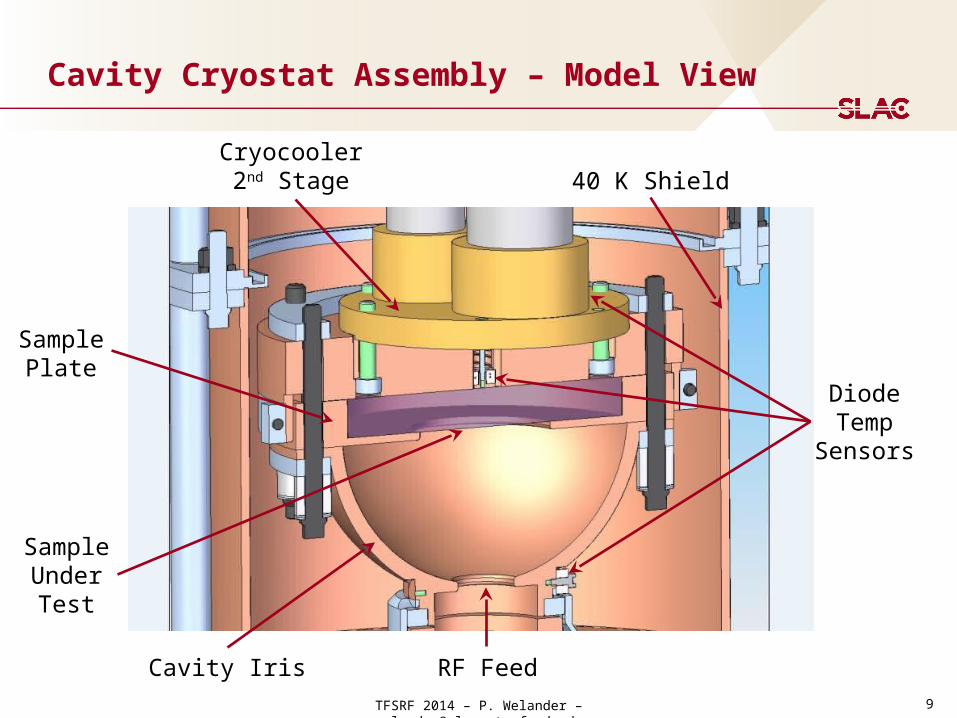
Cavity Cryostat Assembly – Model View
Cryocooler2nd Stage
SampleUnderTest
RF Feed
40 K Shield
DiodeTemp
Sensors
SamplePlate
Cavity Iris
TFSRF 2014 – P. Welander – [email protected]
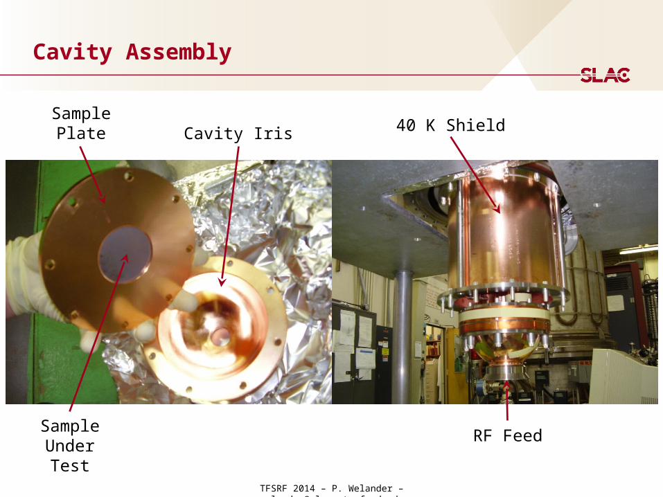
Cavity Assembly
SampleUnderTest
SamplePlate Cavity Iris
RF Feed
40 K Shield
TFSRF 2014 – P. Welander – [email protected]
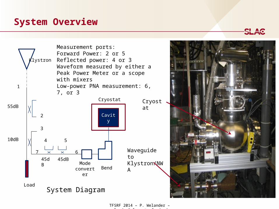
System Overview
Cryostat
Waveguide to Klystron/NWA
Measurement ports:Forward Power: 2 or 5Reflected power: 4 or 3Waveform measured by either a Peak Power Meter or a scope with mixersLow-power PNA measurement: 6, 7, or 3
1
2
3
4
Cavity
Klystron
10dB
45dB 45dB
5
6
55dB
7
Cryostat
Mode converter Bend
LoadSystem Diagram
TFSRF 2014 – P. Welander – [email protected]
5 104
1 105
1.5 105
2 105
2.5 105
0 50 100 150 200 250 300
SLAC Cu sampleLow power test result
Q0Q0
Temperature(K)
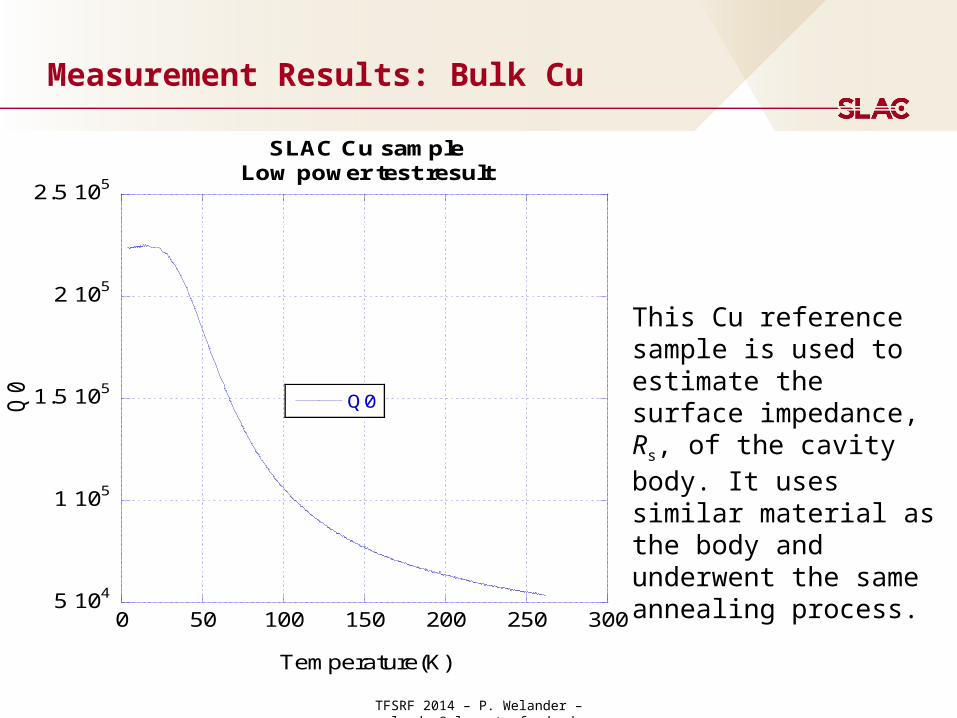
Measurement Results: Bulk Cu
This Cu reference sample is used to estimate the surface impedance, Rs, of the cavity body. It uses similar material as the body and underwent the same annealing process.
TFSRF 2014 – P. Welander – [email protected]
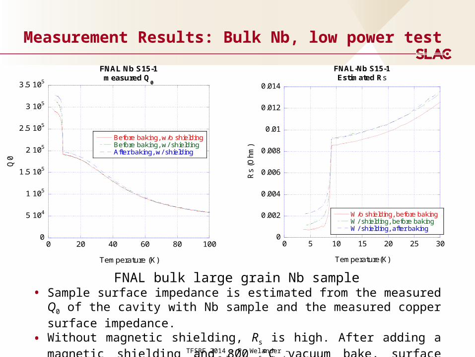
Measurement Results: Bulk Nb, low power test
FNAL bulk large grain Nb sample• Sample surface impedance is estimated from the measured Q0 of the
cavity with Nb sample and the measured copper surface impedance. • Without magnetic shielding, Rs is high. After adding a magnetic shielding
and 800 °C vacuum bake, surface impedance reduced by a factor of 3.
0
0.002
0.004
0.006
0.008
0.01
0.012
0.014
0 5 10 15 20 25 30
FNAL-Nb S15-1Estimated Rs
W/o shielding, before baking W/ shielding, before bakingW/ shielding, after baking
Rs
(Oh
m)
Temperature(K)
0
5 104
1 105
1.5 105
2 105
2.5 105
3 105
3.5 105
0 20 40 60 80 100
FNAL Nb S15-1measured Q
0
Before baking, w/o shieldingBefore baking, w/ shieldingAfter baking, w/ shielding
Q0
Temperature (K)
TFSRF 2014 – P. Welander – [email protected]
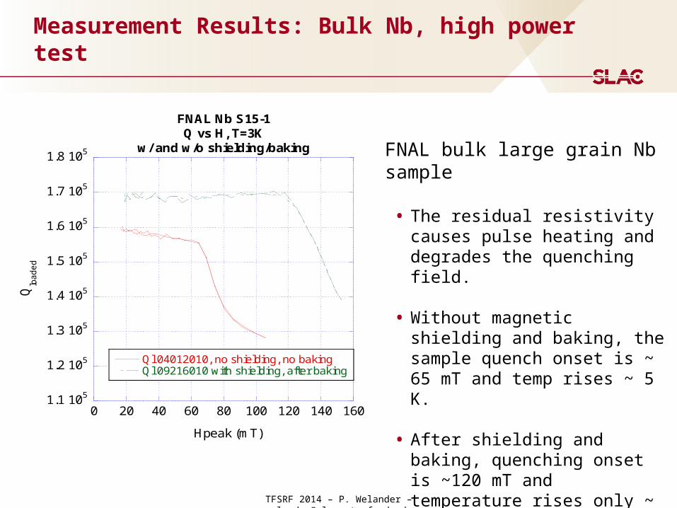
Measurement Results: Bulk Nb, high power test
FNAL bulk large grain Nb sample
• The residual resistivity causes pulse heating and degrades the quenching field.
• Without magnetic shielding and baking, the sample quench onset is ~ 65 mT and temp rises ~ 5 K.
• After shielding and baking, quenching onset is ~120 mT and temperature rises only ~ 3 K.1.1 105
1.2 105
1.3 105
1.4 105
1.5 105
1.6 105
1.7 105
1.8 105
0 20 40 60 80 100 120 140 160
FNAL Nb S15-1Q vs H, T=3K
w/ and w/o shielding/baking
Ql 04012010, no shielding, no bakingQl 09216010 with shielding, after baking
Qlo
ad
ed
Hpeak (mT)
TFSRF 2014 – P. Welander – [email protected]
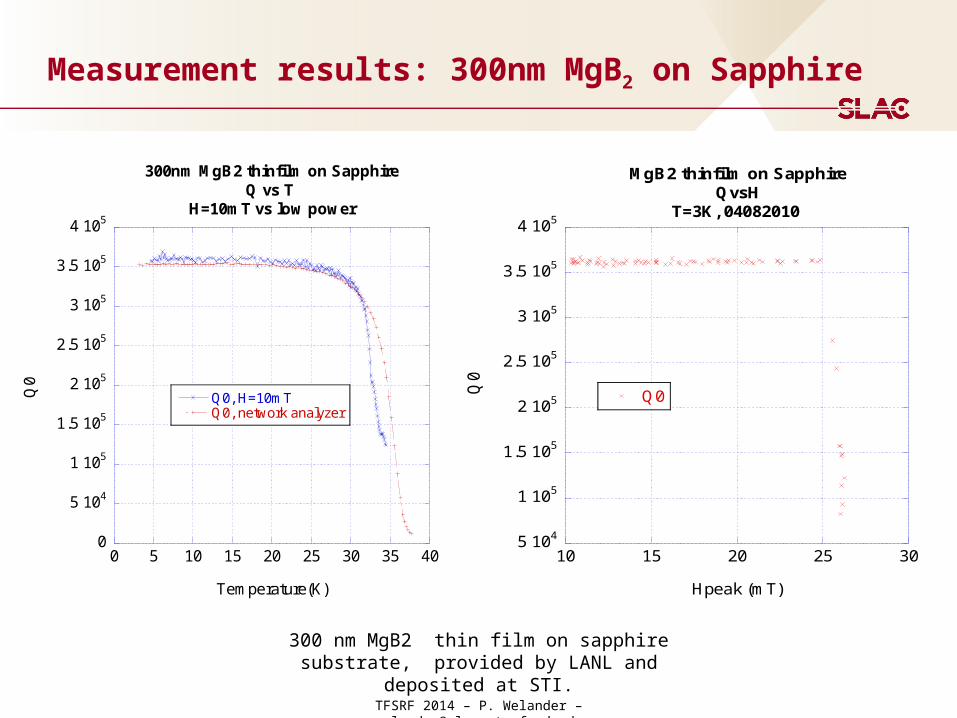
Measurement results: 300nm MgB2 on Sapphire
0
5 104
1 105
1.5 105
2 105
2.5 105
3 105
3.5 105
4 105
0 5 10 15 20 25 30 35 40
300nm MgB2 thinfilm on SapphireQ vs T
H=10mT vs low power
Q0, H=10mTQ0, network analyzer
Q0
Temperature(K)
5 104
1 105
1.5 105
2 105
2.5 105
3 105
3.5 105
4 105
10 15 20 25 30
MgB2 thinfilm on SapphireQvsH
T=3K, 04082010
Q0Q0
Hpeak (mT)
300 nm MgB2 thin film on sapphire substrate, provided by LANL and deposited at STI.
TFSRF 2014 – P. Welander – [email protected]
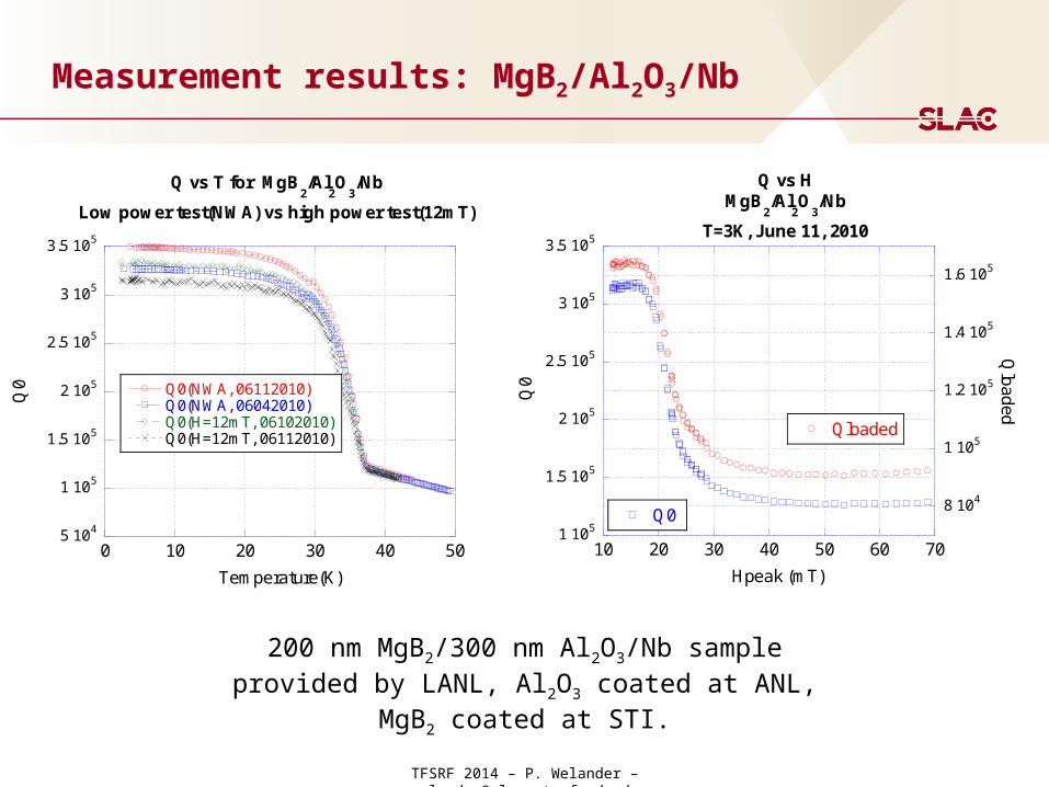
Measurement results: MgB2/Al2O3/Nb
200 nm MgB2/300 nm Al2O3/Nb sample provided by LANL, Al2O3 coated at ANL, MgB2 coated at STI.
1 105
1.5 105
2 105
2.5 105
3 105
3.5 105
8 104
1 105
1.2 105
1.4 105
1.6 105
10 20 30 40 50 60 70
Q vs HMgB
2/Al
2O
3/Nb
T=3K, June 11, 2010
Q0
Qloaded
Q0
Qloa
ded
Hpeak (mT)
5 104
1 105
1.5 105
2 105
2.5 105
3 105
3.5 105
0 10 20 30 40 50
Q vs T for MgB2/Al
2O
3/Nb
Low power test(NWA) vs high power test(12mT)
Q0(NWA, 06112010)Q0(NWA, 06042010)Q0(H=12mT, 06102010)Q0(H=12mT, 06112010)
Q0
Temperature(K)
TFSRF 2014 – P. Welander – [email protected]
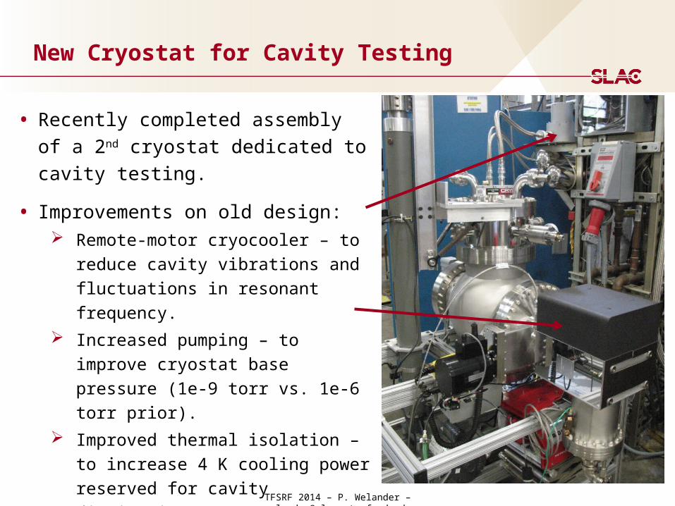
New Cryostat for Cavity Testing
• Recently completed assembly of a 2nd
cryostat dedicated to cavity testing.
• Improvements on old design: Remote-motor cryocooler – to reduce
cavity vibrations and fluctuations in
resonant frequency.
Increased pumping – to improve
cryostat base pressure (1e-9 torr vs.
1e-6 torr prior).
Improved thermal isolation – to
increase 4 K cooling power reserved
for cavity dissipation.
TFSRF 2014 – P. Welander – [email protected]
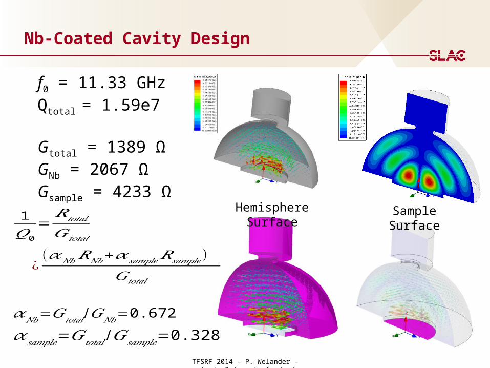
Sample SurfaceHemisphere Surface
f0 = 11.33 GHzQtotal = 1.59e7
Gtotal = 1389 ΩGNb = 2067 ΩGsample = 4233 Ω
Nb-Coated Cavity Design
1𝑄0
=𝑅𝑡𝑜𝑡𝑎𝑙
𝐺𝑡𝑜𝑡𝑎𝑙
¿(𝛼𝑁𝑏𝑅𝑁𝑏+𝛼𝑠𝑎𝑚𝑝𝑙𝑒𝑅𝑠𝑎𝑚𝑝𝑙𝑒)
𝐺𝑡𝑜𝑡𝑎𝑙
𝛼𝑠𝑎𝑚𝑝𝑙𝑒=𝐺𝑡𝑜𝑡𝑎𝑙/𝐺𝑠𝑎𝑚𝑝𝑙𝑒=0.328𝛼𝑁𝑏=𝐺𝑡𝑜𝑡𝑎𝑙 /𝐺𝑁𝑏=0.672
20TFSRF 2014 – P. Welander – [email protected]
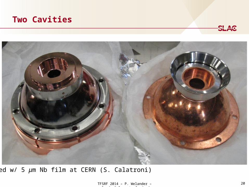
Two Cavities
Coated w/ 5 μm Nb film at CERN (S. Calatroni)
21TFSRF 2014 – P. Welander – [email protected]
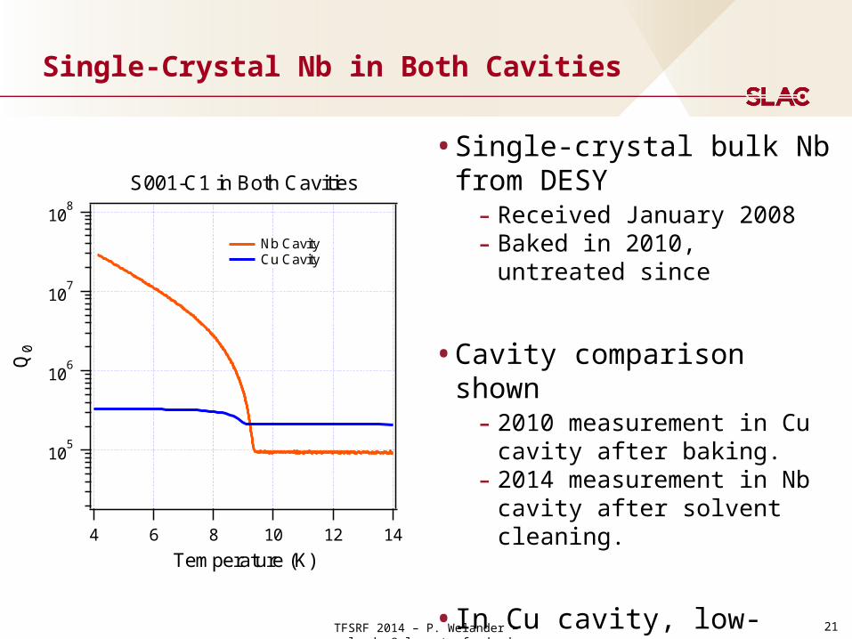
Single-Crystal Nb in Both Cavities
• Single-crystal bulk Nb from DESY
- Received January 2008- Baked in 2010, untreated since
• Cavity comparison shown- 2010 measurement in Cu
cavity after baking.- 2014 measurement in Nb
cavity after solvent cleaning.
• In Cu cavity, low-temperature Q0 is limited by Cu surface resistance.
105
106
107
108
Q0
141210864
Temperature (K)
S001-C1 in Both Cavities
Nb Cavity Cu Cavity
22TFSRF 2014 – P. Welander – [email protected]
4
6
0.1
2
4
6
1
2
4
6
10
2
Rs
(m
4 5 6 7 8 910
2 3
Temperature (K)
S001-C1 in Nb Cavity
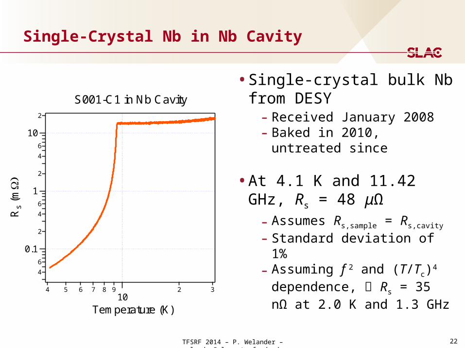
Single-Crystal Nb in Nb Cavity
• Single-crystal bulk Nb from DESY
- Received January 2008- Baked in 2010, untreated since
• At 4.1 K and 11.42 GHz, Rs = 48 μΩ
- Assumes Rs,sample = Rs,cavity
- Standard deviation of 1%- Assuming f 2 and (T/Tc)4
dependence, Rs = 35 nΩ at 2.0 K and 1.3 GHz

TFSRF 2014 – P. Welander – [email protected]
Thin Film Deposition
• Collaborative effort with Mac Beasley
(Applied Physics) & Bruce Clemens
(Materials Science) at Stanford
• 3-target sputtering system being
utilized for deposition on 2” wafers.
• Elemental targets and nitrogen gas
used for reactive DC sputtering of
nitride films.
• Recently started thin-film growth
development with Nb films, followed
by NbN and NbTiN.Characterize materials using analysis tools at the Stanford Nano Center (e.g. XRD, XPS, TEM)
TFSRF 2014 – P. Welander – [email protected]
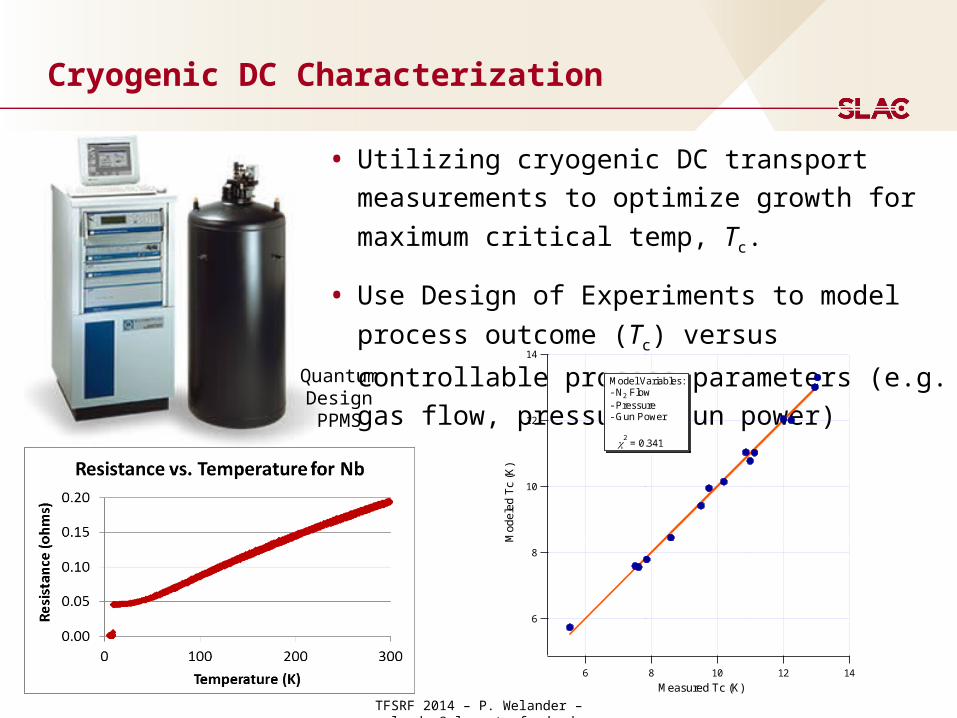
Cryogenic DC Characterization
• Utilizing cryogenic DC transport measurements to
optimize growth for maximum critical temp, Tc.
• Use Design of Experiments to model process
outcome (Tc) versus controllable process
parameters (e.g. gas flow, pressure, gun power)14
12
10
8
6
Mod
eled
Tc
(K)
14121086
Measured Tc (K)
Model Variables: - N2 Flow - Pressure - Gun Power
2 = 0.341
Quantum DesignPPMS
TFSRF 2014 – P. Welander – [email protected]
Summary
• Cryogenic RF testing underway again at SLAC
• New cryostat dedicated to SRF materials evaluation
• Working toward NbN and NbTiN film growth
• Two cavities (Cu & Nb) for sample characterization
- Hquench up to 360 mT, Rs with sub-nΩ resolution
• Low-power Q vs. T takes less than 24 hrs.
• Send us your samples!
Top Related