


Languages
Pages
Legal


P08009Audible Memo Board
Phase II
Monday, October 22, 2007P08009: Audible Memo Board Phase II
Sponsor: Tala Hopkins
Jon Gosliga Audio Output Lead
Loic Hureau Audio Input Lead
Jim Varghese Audio Lead
Alex Gorevski Software Logic & Signal Conversion Lead
Project Description
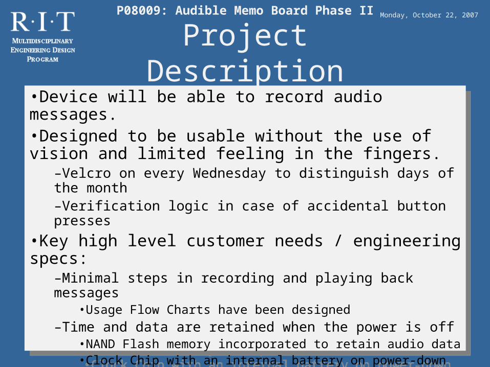
•Device will be able to record audio messages.•Designed to be usable without the use of vision and limited feeling in the fingers.
–Velcro on every Wednesday to distinguish days of the month–Verification logic in case of accidental button presses
•Key high level customer needs / engineering specs:–Minimal steps in recording and playing back messages
•Usage Flow Charts have been designed
–Time and data are retained when the power is off•NAND Flash memory incorporated to retain audio data•Clock Chip with an internal battery on power-down
–The user can record, delete, and playback messages & the messages are easy to find
•Software Flowcharts have been designed
Monday, October 22, 2007P08009: Audible Memo Board Phase II

Video Demonstration
Monday, October 22, 2007P08009: Audible Memo Board Phase II

Design ConceptCalendar Mode
Monday, October 22, 2007P08009: Audible Memo Board Phase II
Erase
Playback
Record
Change Month
Next/Previous Message
Calendar

Design ConceptMemo Mode
Monday, October 22, 2007P08009: Audible Memo Board Phase II
Playback
Record
Different Memos
Clock
Mode Change
Volume

System Architecture
Monday, October 22, 2007P08009: Audible Memo Board Phase II
Microphone
Amplification
Band Pass Filter
Microprocessor
Debug Terminal
Memory Storage
Software Logic
ADC Timer
D-A Converter
KeyboardIO
Ports
Speaker
Amplification
Filter
Software Logic
Monday, October 22, 2007P08009: Audible Memo Board Phase II
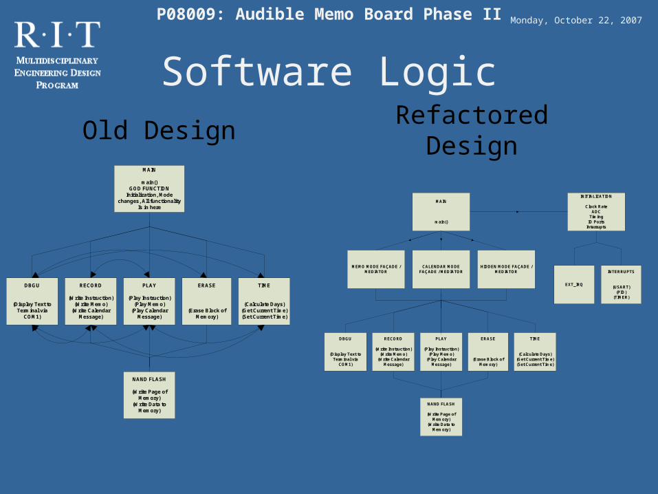
MAIN
main()GOD FUNCTION
Initialization, Mode changes, All functionality
Is in here
DBGU
(Display Text to Terminal via
COM1)
RECORD
(Write Instruction)(Write Memo)
(Write Calendar Message)
PLAY
(Play Instruction)(Play Memo)
(Play Calendar Message)
ERASE
(Erase Block of Memory)
TIME
(Calculate Days)(Get Current Time)(Set Current Time)
NAND FLASH
(Write Page of Memory)
(Write Data to Memory)
Old Design Refactored Design
MAIN
main()
INITIALIZATION
Clock RateADC
TimingIO Ports
Interrupts
MEMO MODE FAÇADE / MEDIATOR
CALENDAR MODE FAÇADE / MEDIATOR
HIDDEN MODE FAÇADE /MEDIATOR
DBGU
(Display Text to Terminal via
COM1)
RECORD
(Write Instruction)(Write Memo)
(Write Calendar Message)
PLAY
(Play Instruction)(Play Memo)
(Play Calendar Message)
ERASE
(Erase Block of Memory)
TIME
(Calculate Days)(Get Current Time)(Set Current Time)
NAND FLASH
(Write Page of Memory)
(Write Data to Memory)
EXT_IRQ
INTERRUPTS
(USART)(PIO)
(TIMER)

Technical Risk Assessment
•Risk: PCB Design difficulty and Proposed Mitigation–How many boards need to be developed?
One board will be designed, which includes filters and amps for both the input and output stages of the circuit–How will we implement the power circuit?
The power circuit will be designed on perf. board to save PCB costs (space saved)–Alternative evaluation board available?
The current evaluation board will be integrated into the design–How will the boards be mounted to the box?
The screws used will be flat-heads in which 4 holes will be drilled in the box. Standoffs will be used to hold the board above the surface of the box
Monday, October 22, 2007P08009: Audible Memo Board Phase II
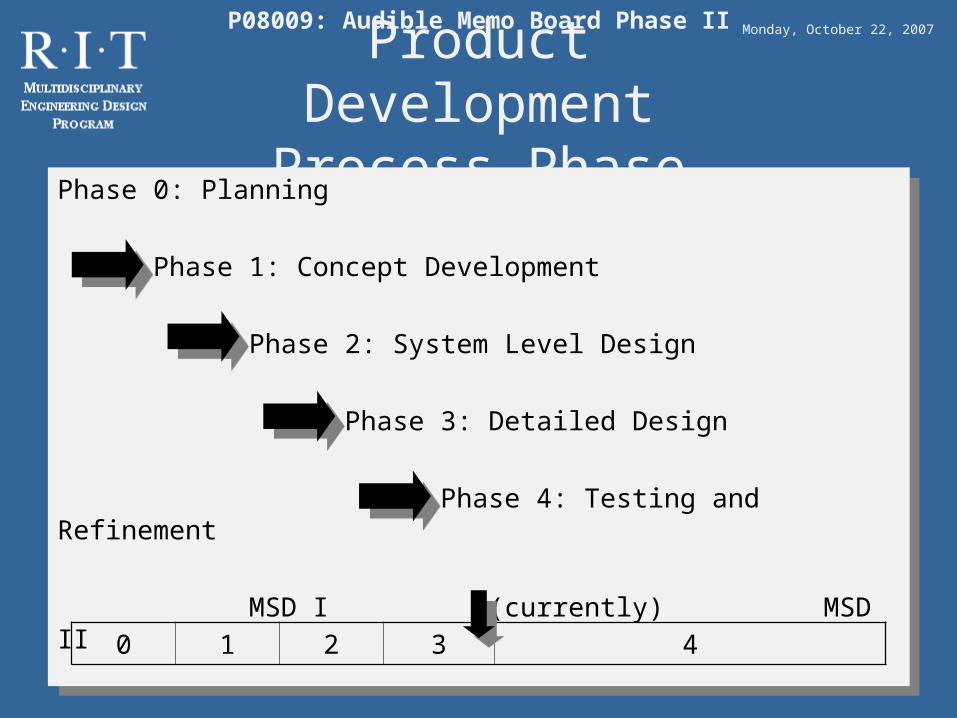
Product Development Process Phase
Phase 0: Planning
Phase 1: Concept Development
Phase 2: System Level Design
Phase 3: Detailed Design
Phase 4: Testing and Refinement
MSD I (currently) MSD II
Phase 0: Planning
Phase 1: Concept Development
Phase 2: System Level Design
Phase 3: Detailed Design
Phase 4: Testing and Refinement
MSD I (currently) MSD II
Monday, October 22, 2007P08009: Audible Memo Board Phase II
0 1 2 3 4

Current State of Design
•Functional Components–Audio input circuit–Audio output circuit–NAND Flash Audio Storage–Majority of software logic
•The Clock chip is being ordered so that the last of the functional requirements may be met
•Remaining software logic for the clock chip and small bug fixes
•Filtering needs refinement to reduce noise
•The project cost will rise due to the PCB Design–Old Design cost $435.95–New Design will cost ~$280
•$60 uController and Clock Chips•$15 Headers, surface-mount resistors and capacitors•$215 for the Printed Circuit Board
Monday, October 22, 2007P08009: Audible Memo Board Phase II

MSD II Project Schedule Milestones
•11/16/07: Finish the testing for the clock chip
•12/10/07: Finish the development of the PCB layout
•12/10/07: Order all parts and send out PCB design for fabrication
•12/13/07: Begin testing the design with the PCB and make changes where necessary.
•12/13/07: Finalize device code, finalize documentation.
•1/30/08: Finish building, test final product with customer.
•Mid February: Functional and performance review.
•End of February: Final product review.
Monday, October 22, 2007P08009: Audible Memo Board Phase II
Thank you for attending.
Questions?
Monday, October 22, 2007P08009: Audible Memo Board Phase II
Top Related