


Languages
Pages
Legal

Overview•Logic
•Combinational Logic
•Sequential Logic
•Storage Devices
• SR Flip-Flops
• D Flip Flops
• JK Flip Flops
• Registers
• Addressing
• Computer Memory
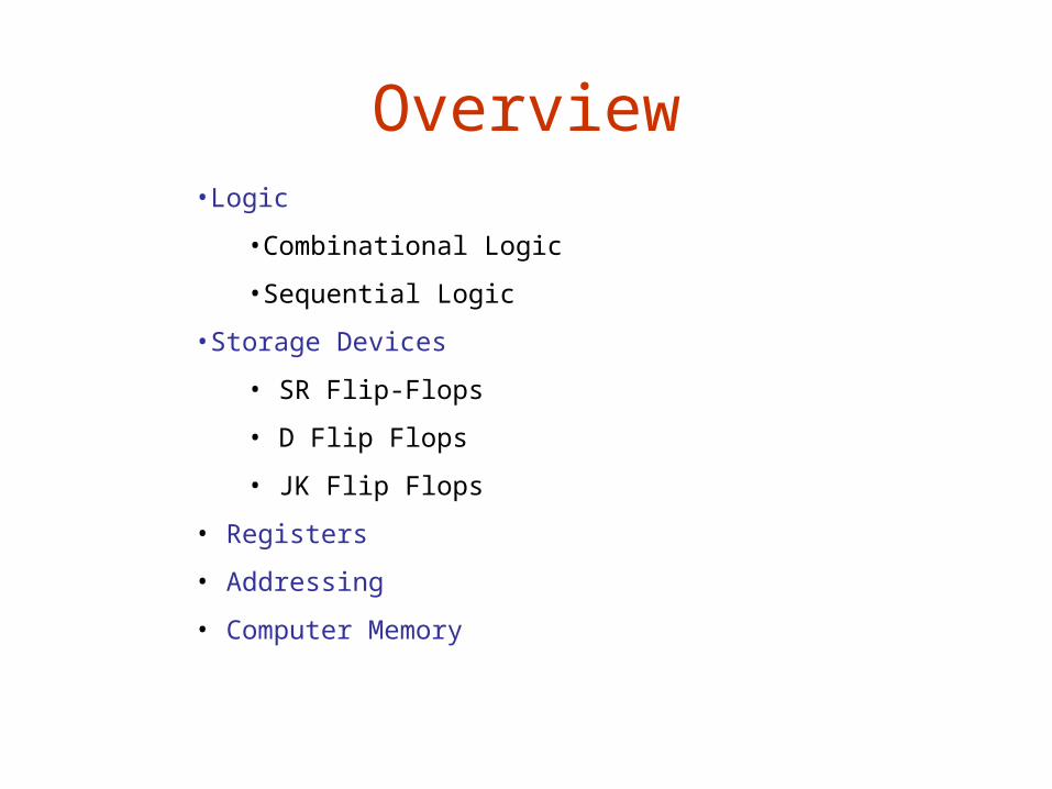
Logical Completeness
•Can implement ANY truth table with AND, OR, NOT.
A B C D
0 0 0 0
0 0 1 0
0 1 0 1
0 1 1 0
1 0 0 0
1 0 1 1
1 1 0 0
1 1 1 0
1. AND combinations that yield a "1" in the truth table.
2. OR the resultsof the AND gates.
Combinational vs. Sequential
•Combinational Circuit– always gives the same output for a given set of inputs
• ex: adder always generates sum and carry,regardless of previous inputs
•Sequential Circuit– stores information– output depends on stored information (state) plus input
• so a given input might produce different outputs,depending on the stored information
– example: ticket counter• advances when you push the button• output depends on previous state
– useful for building “memory” elements and “state machines”
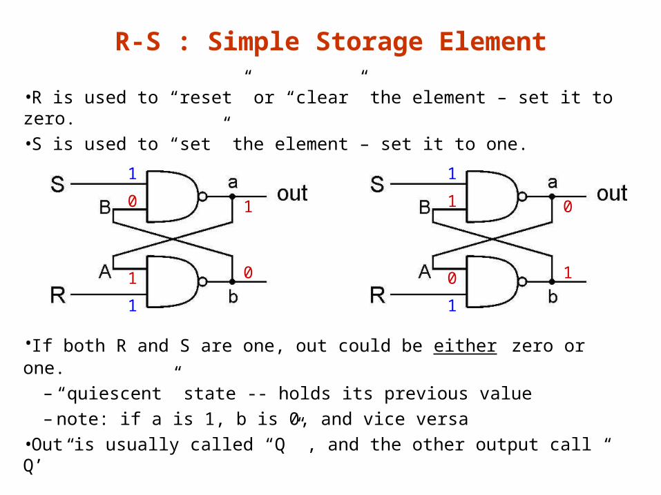
R-S : Simple Storage Element
•R is used to “reset” or “clear” the element – set it to zero.•S is used to “set” the element – set it to one.
•If both R and S are one, out could be either zero or one.
– “quiescent” state -- holds its previous value– note: if a is 1, b is 0, and vice versa
•Out is usually called “Q” , and the other output call “ Q’ ”
1
0
1
1
1
1
0
0
1
1
0
0
1
1
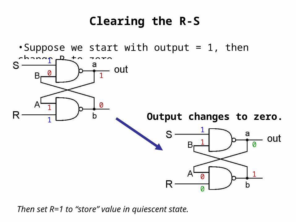
Clearing the R-S
•Suppose we start with output = 1, then change R to zero.
Output changes to zero.
Then set R=1 to “store” value in quiescent state.
1
0
1
1
1
1
0
0
1
0
1
0
0
0
1
1
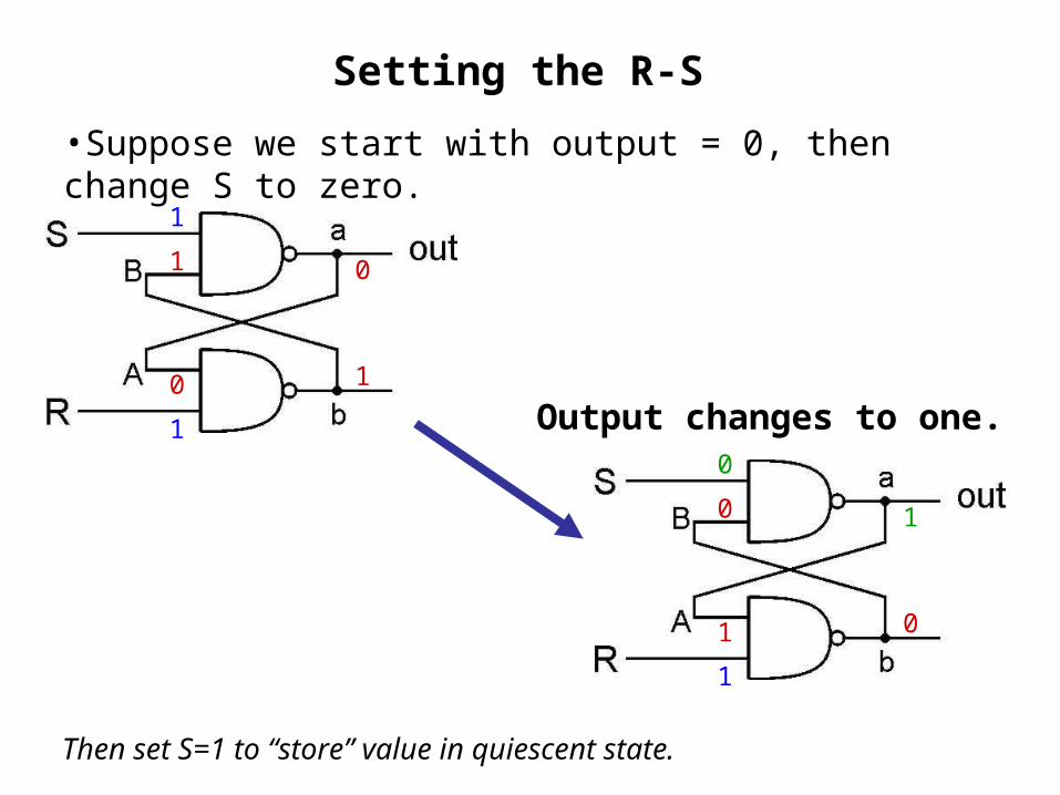
Setting the R-S
•Suppose we start with output = 0, then change S to zero.
Output changes to one.
Then set S=1 to “store” value in quiescent state.
1
1
0
0
1
1
0
1
1
1
0
0
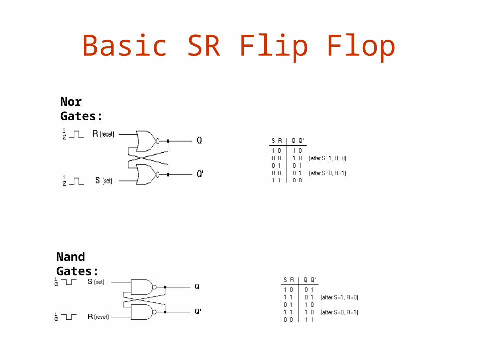
Basic SR Flip Flop
Nor Gates:
Nand Gates:
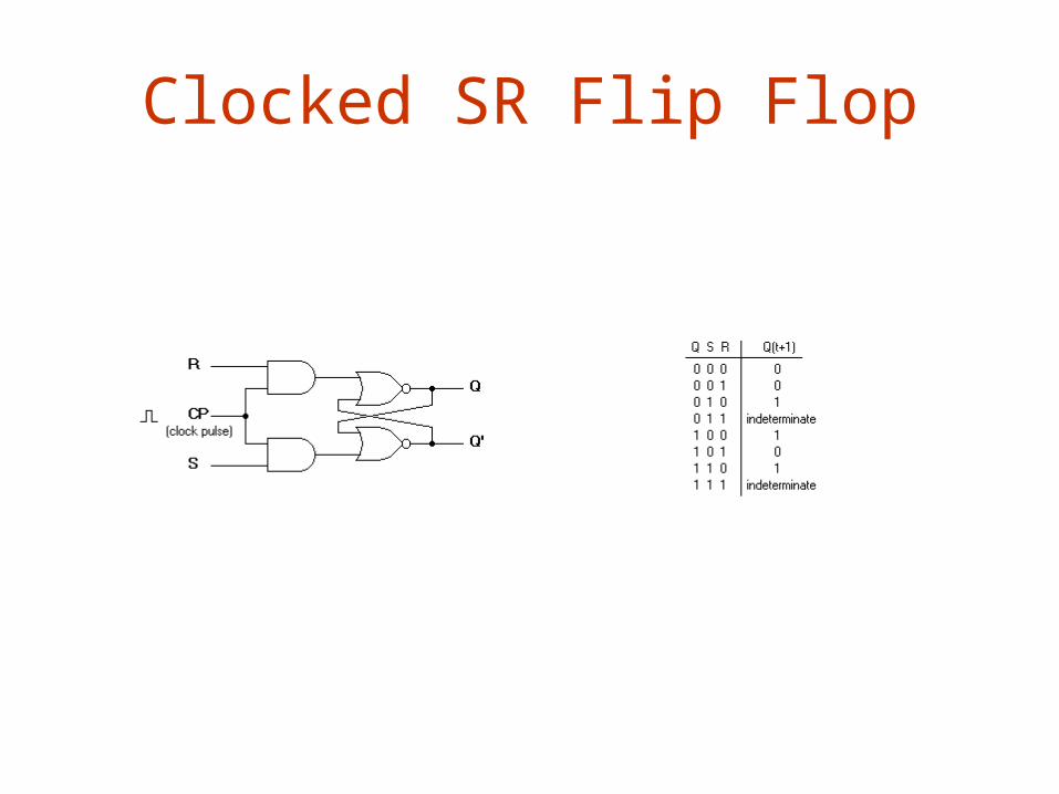
Clocked SR Flip Flop
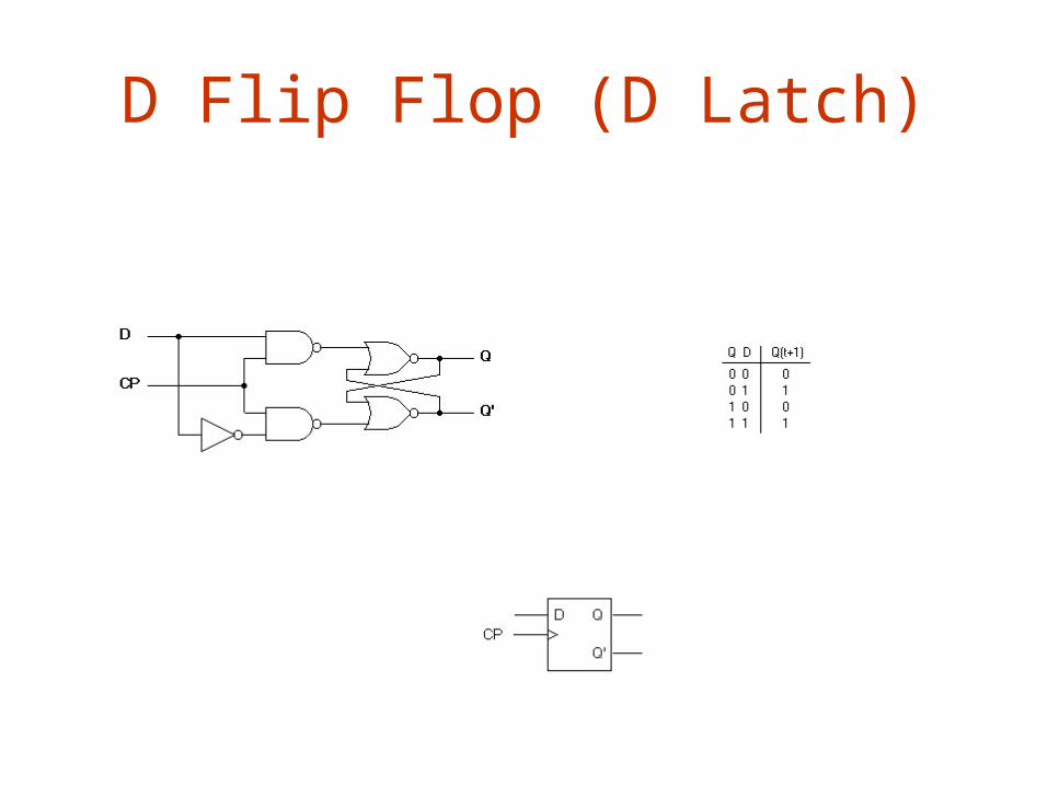
D Flip Flop (D Latch)
D-Latch
•Two inputs: D (data) and WE (write enable)– when WE = 1, latch is set to value of D
• S = NOT(D), R = D– when WE = 0, latch holds previous value
• S = R = 1
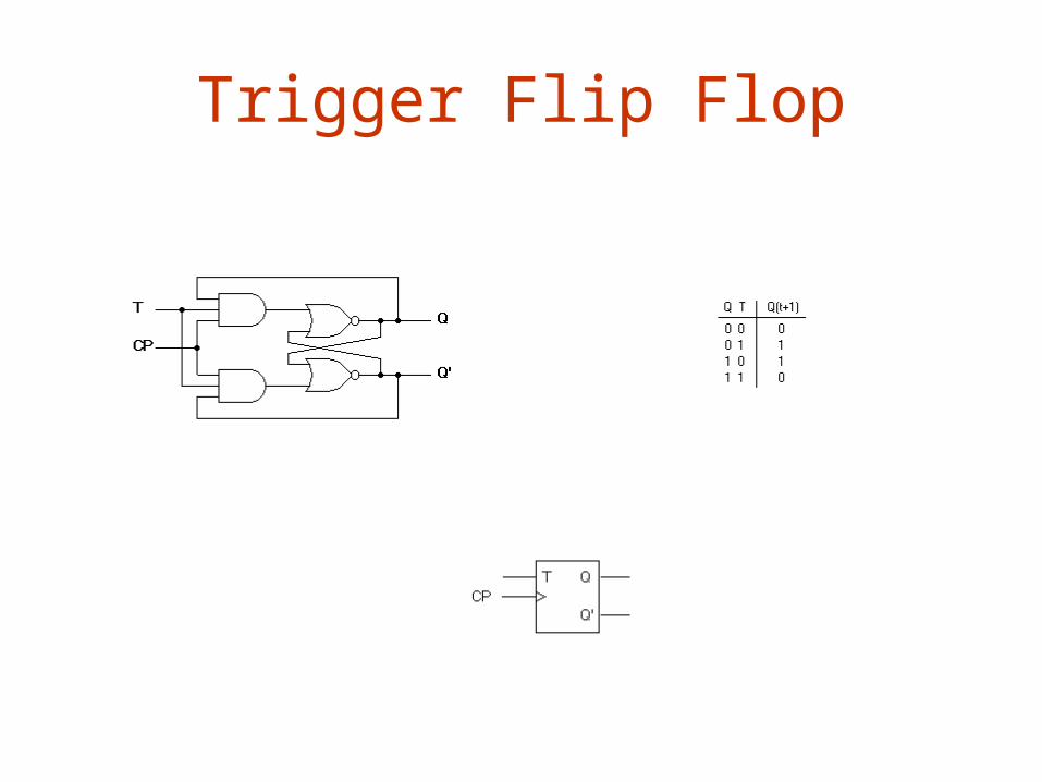
Trigger Flip Flop
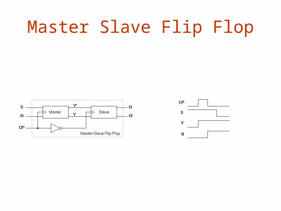
Master Slave Flip Flop
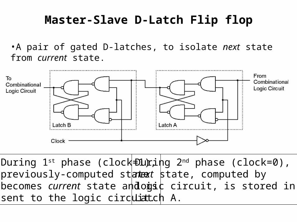
Master-Slave D-Latch Flip flop
•A pair of gated D-latches, to isolate next state from current state.
During 1st phase (clock=1),previously-computed statebecomes current state and issent to the logic circuit.
During 2nd phase (clock=0),next state, computed bylogic circuit, is stored inLatch A.
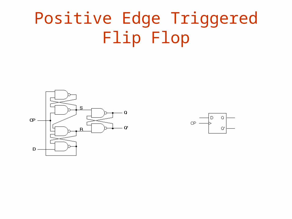
Positive Edge Triggered Flip Flop
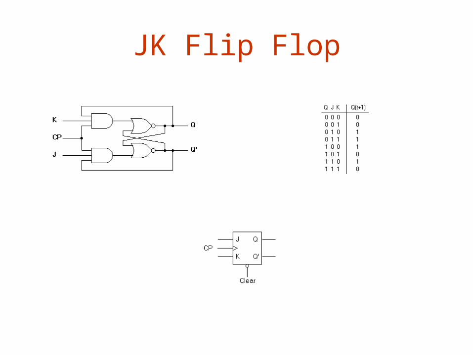
JK Flip Flop
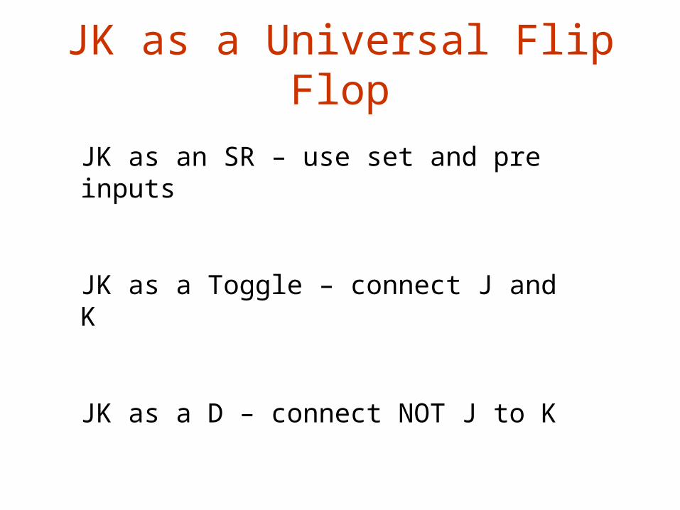
JK as a Universal Flip Flop
JK as an SR – use set and pre inputs
JK as a Toggle – connect J and K
JK as a D – connect NOT J to K
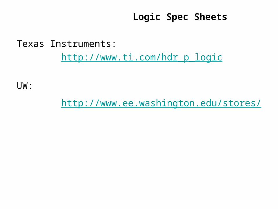
Logic Spec Sheets
Texas Instruments:
http://www.ti.com/hdr_p_logic
UW:
http://www.ee.washington.edu/stores/
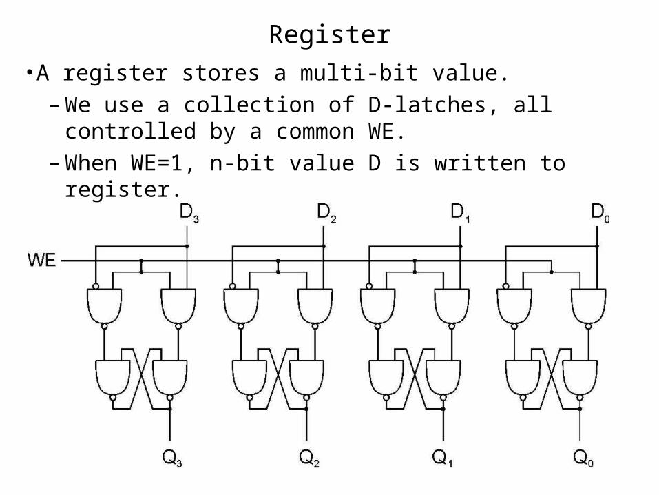
Register
•A register stores a multi-bit value.– We use a collection of D-latches, all controlled by a
common WE.– When WE=1, n-bit value D is written to register.
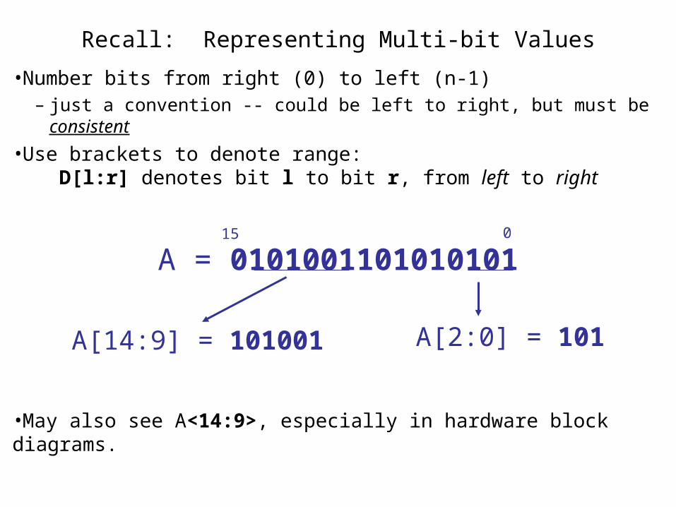
Recall: Representing Multi-bit Values
•Number bits from right (0) to left (n-1)– just a convention -- could be left to right, but must be consistent
•Use brackets to denote range: D[l:r] denotes bit l to bit r, from left to right
•May also see A<14:9>, especially in hardware block diagrams.
A = 0101001101010101
A[2:0] = 101A[14:9] = 101001
015
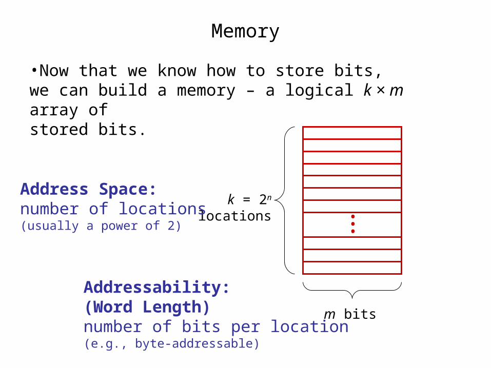
Memory
•Now that we know how to store bits,we can build a memory – a logical k × m array of stored bits.
•••
k = 2n
locations
m bits
Address Space:number of locations(usually a power of 2)
Addressability:(Word Length)number of bits per location(e.g., byte-addressable)
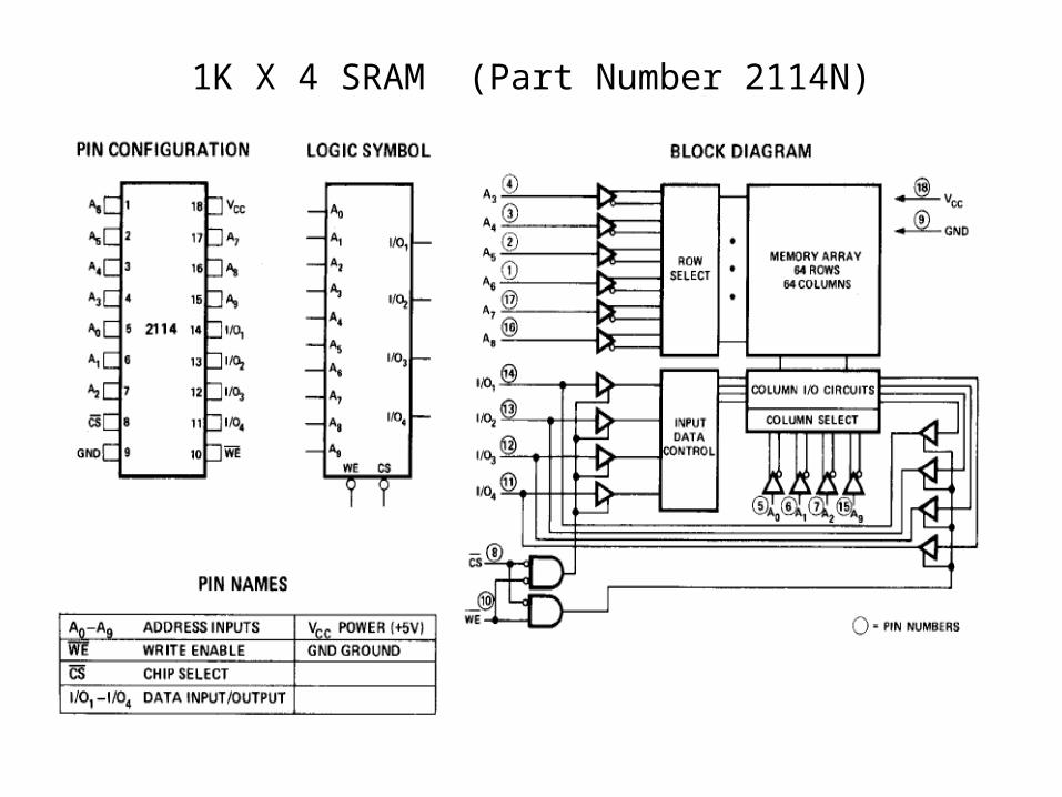
1K X 4 SRAM (Part Number 2114N)
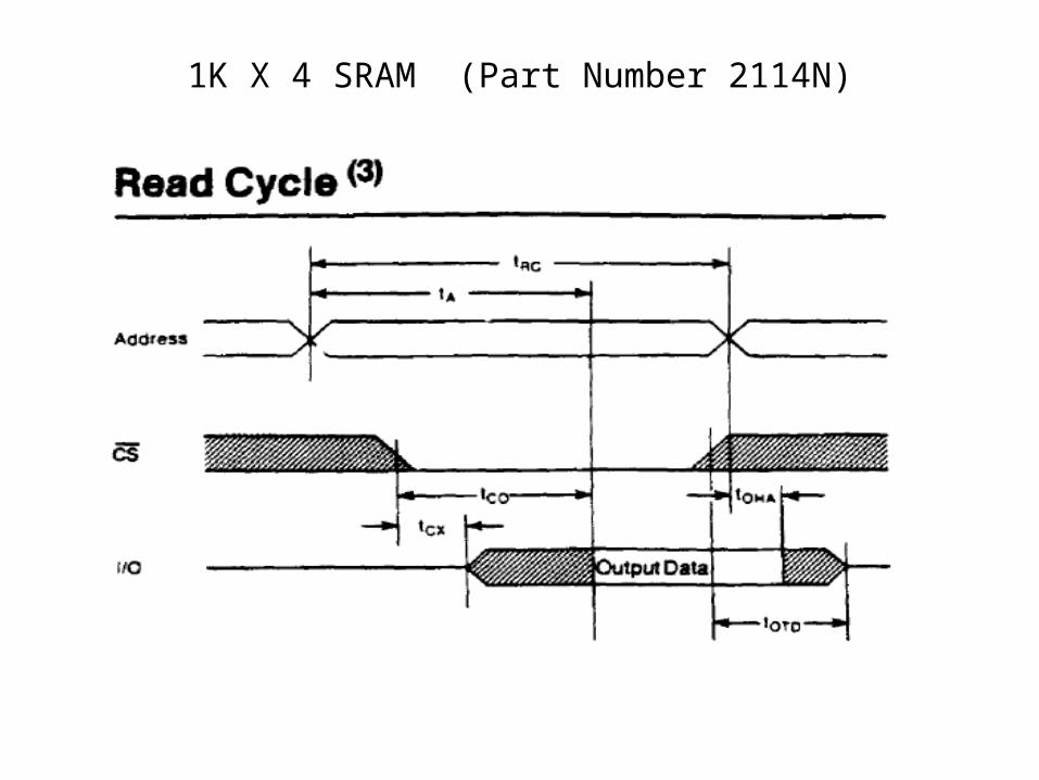
1K X 4 SRAM (Part Number 2114N)
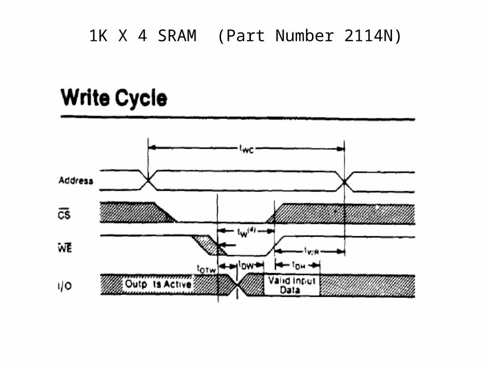
1K X 4 SRAM (Part Number 2114N)
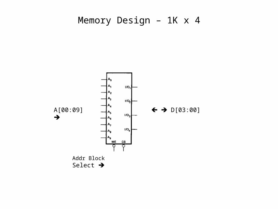
Memory Design – 1K x 4
A[00:09] D[03:00]
Addr Block Select
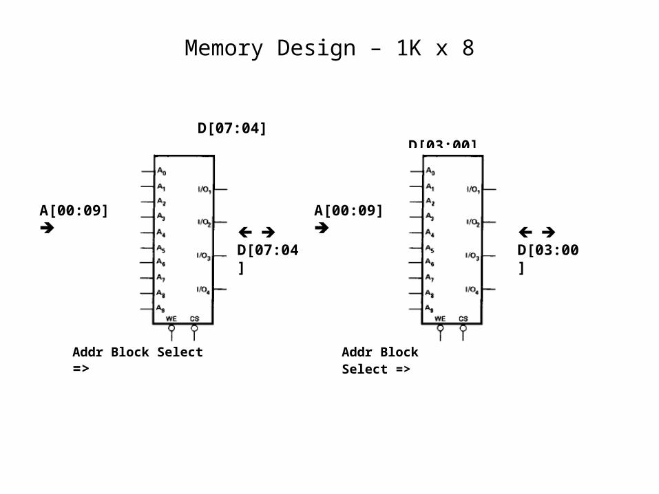
Memory Design – 1K x 8
A[00:09] D[07:04]
A[00:09] D[03:00]
Addr Block Select => Addr Block Select =>
D[07:04] D[03:00]
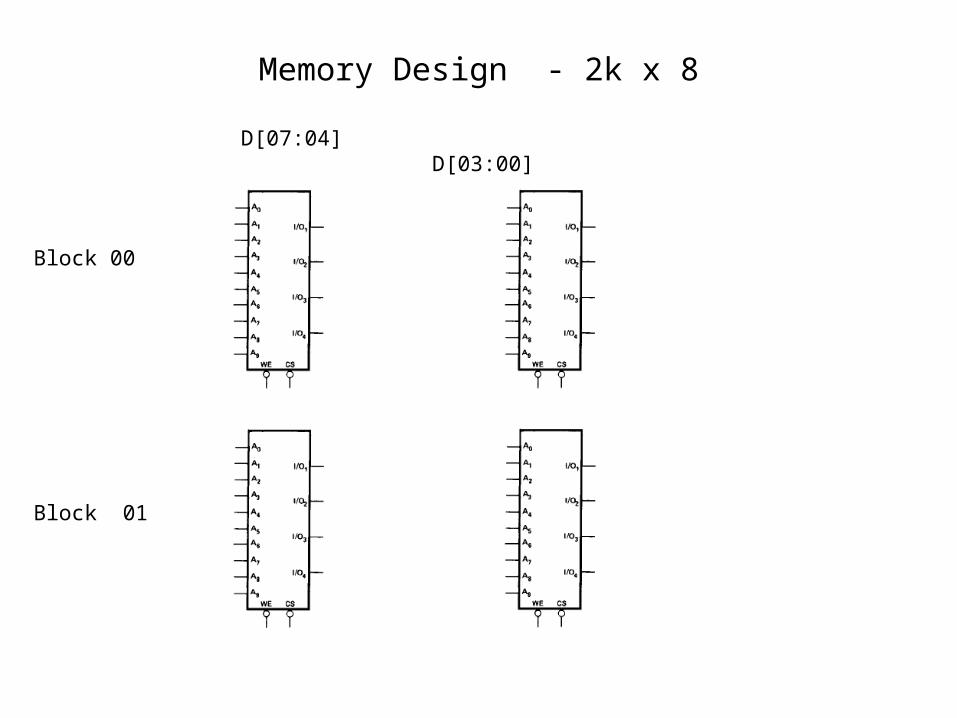
Memory Design - 2k x 8
D[07:04] D[03:00]
Block 00
Block 01
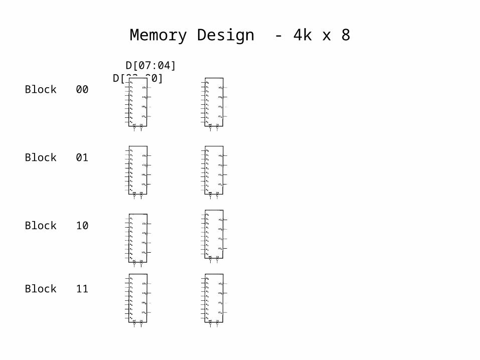
Memory Design - 4k x 8
D[07:04] D[03:00]
Block 00
Block 01
Block 10
Block 11
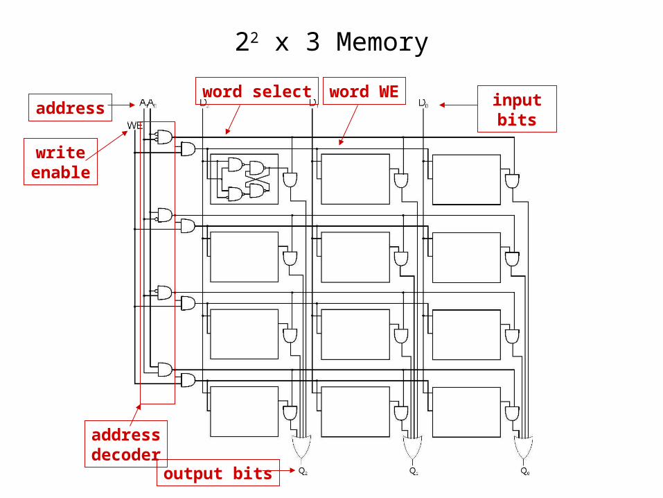
22 x 3 Memory
addressdecoder
word select word WEaddress
writeenable
input bits
output bits
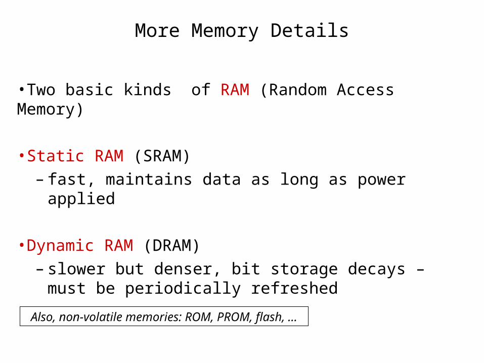
More Memory Details
•Two basic kinds of RAM (Random Access Memory)
•Static RAM (SRAM)– fast, maintains data as long as power applied
•Dynamic RAM (DRAM)– slower but denser, bit storage decays – must be
periodically refreshed
Also, non-volatile memories: ROM, PROM, flash, …
Top Related