


Languages
Pages
Legal


©HDP User Group International, Inc. 1
Optical Interconnect Project
Project Update M.Immonen, TTM Meadville, Shaoyong Xiang, Huawei
For Member Meeting St Clara USA
January 9, 2011
©HDP User Group International, Inc. 1
Definition Stage Project

Background
• Increasing data rates in high-speed cards/backplanes
• Initiatives for serial signaling > 20 Gbps per lane over copper
interconnects – e.g. CEI 25G/28G VSR or IEEE 802.3ba 100G Cu
Backplane
• Some of the designs have board-to-board (B2B) signal reach
requirements of one meter through two sets of B2B connectors
• Significant increase in cost/ power consumption/ design efforts/
manufacturing challenges to achieve viable 20+ Gbps operation
• AOCs are becoming dominant for longer links (> 2m)
• Could fiber/waveguide interconnects mitigate some challenges?
• Maybe, if
• Providing very high speed or high bandwidth density
• Reducing power consumption
• Comparable cost
• Maturity, eco-system and proven reliability
©HDP User Group International, Inc. 2

Purpose
• Understanding performance benefits and limitations using
optical fibers and polymer waveguides for intra-system
interconnects on cards and backplanes
• Demonstrate backplane architecture that shows cost/
performance improvements obtained by using FO/WG links
• Focus on optical fiber/WG link characteristics, connectivity,
end-to-end link implementations and reliability of the same
• Use ―Black-box‖ approach, standardized components and
interfaces, be protocol-agnostic, focus on practical
solutions
©HDP User Group International, Inc. 3
Goals and Approach
• SoA survey of WG materials, parallel optical xceivers and
connectors available for short reach optical links
• Build verification TV (TV1) with multiple waveguide components
and FO/WG connects to examine practicality and link metrics
• Build a more complex system-level demonstration TV (TV2)
• Compare test results to equivalent electrical links and identify
design characteristics unique to optical signaling
• Assess optical backplane reliability using the TV constructions
with selected WG/FO designs, connectors and module packages
• Point out gaps and issues in design, fabrication, assembly and
testing to be addressed in the industry/ follow-on projects
• Provide robust technology building-blocks and best-practices for
System designers/ users/ providers
©HDP User Group International, Inc. 4
Out of Scope/ Project will not Provide
• Build application specific prototype(s)
• Solutions based on WDM or single mode fibers/WGs
• Wavelengths of 2nd and 3rd window
• Communication architectures other than point-to-point
• Need for multi-protocol module support
• Transceivers limited to mount at the card edge
• Chip-level photonic networks and Si-pho device
©HDP User Group International, Inc. 5

S.Xiang/Huawei,
B.Achir/Cisco,
M.Marino/Juniper,
C.Nodding/Boeing,
M.Brachmann/ALu,
D.Smith/NGC
B.Booth/OIL,
M.Immonen/TTM,
T.Shutter/Dow,
J.Rennie/API
R.Pitwon/Xyratex,
D.Richardson/Molex,
D.Rolston/Reflex Pho.
Sub-teams and Tasks
System Architecture and Specifications
• Optical intra-system link architectures
• Definition and specification of test vehicles
• Definition of optical layer interfaces and
signal launch
Design Architecture team
• Design practices for optical/electrical boards
Waveguide and fiber interconnects
• WG and FO materials and their data
• Optical waveguide processing and testing
Transceivers and Connectors
• Devices and connectors
• Data and link comparisons
©HDP User Group International, Inc. 6

Project Test Vehicles
• Verification Test Vehicle (TV1)
• Backplane with connector interfaces
• Used to verify design parameters and devices selected for TV2
• Basic TV, basic performance and reliability testing by the team
• Currently 3 available WG technologies to build TV1
• Specification and design must fit all WG technologies
• Design to include multiple WG components fitting realistic application targets
• Connector interfaces that can be used for performance testing and for
interfacing by OEMs and others to evaluate specific applications
• May want to include at least one daughter card with some kind of function on it
to test the backplane interface
• Must allow application/company specific tests and interoperability testing
• Demonstration Test Vehicle (TV2)
• Backplane with N Line Card(s) and M Switch Card(s)
• More difficult TV, Enhanced testing by the team
• Expanded specification challenging the technologies
• Connector interfaces that can be used for performance testing and for
interfacing by OEMs and others to evaluate specific applications
• Must allow application/company specific tests and interoperability testing
7

TV1 Concept
©HDP User Group International, Inc. 8
Group 1
Waveguides,
WG-Fiber
Interface
Group 3
Off-chip
Interface
Group 2
End-to-End
Links &
Connectors
A
B
C
Tx/Rx Tx/Rx
E F
G
Card1
N+N channels
Straight WGs, Inner Layer
Straight WGs, Surface Layer
Crossings Cascading bends D
Card2
H WGs + 90° Out-of-plane
Connector2
Connector1 Long waveguide spiral
90° -in-plane bends
1xN couplers
Butt-joint, 90-turn
TBD: Reference copper line designs, connector types (FO/FO; WG/FO; WG/WG)

9 ©HDP User Group International, Inc.

• Board
• Layout, construction, thickness, materials, size – TBD
• Optical layer: 3 polymer waveguide materials (OIL, Dow, API)
• Loss: < 0.1dB/cm; NA 0.2-0.28; 0.24; 0.37
• Core size: 35 µm and up, pitch: 250µm length: 0.15-1m
• End-facet: Butt-joint (90° turn?)
• Fibers: Standard OM3+ 50/125 GI MMF NA=0.2 12-ch fiber/ribbon;
High-NA large-core MMF (NA> 0.3; core > 70 µm)
• Transceivers and optical interface
• Fiber-pigtailed mid-board Optical Engines: available, provider TBD
• Available in 12x10G SMD modules
• Pre-aligned GaAs VCSEL/PDs, Driver, TIA/LA, control and
monitoring functions, FO interface: 50/125 MMF
• Fiber-less mid-board Optical Engines: available, provider TBD
• 4+4 ..12+12 I/O’s, free-space I/O to WGs
• Interface: Butt-couple or Integrated lens
• Connectors
• FO/FO MTP BP connector: orthogonal avail., 90° custom
• WG/FO connector: MT-based custom
• WG/WG BP connector: MT-based custom
TV1 BOM Optics
10

Optical Modules and Interface
©HDP User Group International, Inc. 11
Fibers
Nx12F
Fib
ers
Nx
12
F
E/O/E
conv.
Fib
ers
Nx
12
F
Fibers
Nx12F
E/O/E
conv.
1. Fiber-pigtailed Mid-board Parallel Optical Modules
Source: Hdpug Opto Project Parallel Optical Connector Technology Survey (Rev 020211)
• Optical I/O close IC
• Avoids long high-speed traces on PCB
• BGA/ LGA package with MT or top attached
optical connector
• 120 Gbps per module (12x10 Gbps Tx or Rx)
• Scalable e.g. 1 Tbps in 3 inch2 area
• Power: 45 mW per channel
On card On host module

Waveguides
E/O
conv.
Optical Modules and Interface, cont.
• Surface mountable optical
engines mounted to access
waveguides on board
• Butt-couple (free-space), no
need for 90-deg turn in WG
• Integrated lens array, need for
90-deg turn in WG
• 120 Gbps per module (12x10
Gbps Tx or Rx)
12
WG
/Fib
ers
2. Fiber-less Optical Modules

Testing Plan for TV1
©HDP User Group International, Inc. 13
Fabricate Boards
As-built Testing
Waveguides: IL, TL, RL, Eye 20 GHz, refractive index
Electrical: Impedance, S-parameters, Eye 20 GHz
Connectors: IL, RL, mate/unmate 200 cycles
Transceivers: Pout, Eye, BER
Link: IL, Eye, BER
TC -40/+85C
Link parts. System test In-situ monitoring of IL at established read points
Link BER, before/after
6x 260C
Reflow
Phase I tests to ensure waveguides and interfaces are practical
(or can be made so), they meet the specification Design envelopes for waveguide passive components – Loss vs.
length, size, ROC, # of crossings at NA’s 0.2-0.3
Connector parameters: IL, connector insertion force, # of insertions
before deterioration
Xceives and off-chip interface: Fiber-ended OE, Butt-joint OE
End-to-End Link losses: Macro loss budget
Other: Power vs. copper, functionality change vs. copper

Testing Plan
14 ©HDP User Group International, Inc.
HDPUG Optical Interconnect Project
Testing Plan
** Draft ** Last update 3.2.2011
Proposed Tests and Related Criteria for HDPUG Optical Interconnect TV1 and TV2 Test
Level TV1 TV2 Test Test Condition Test Specification Criteria (proposed) Pot. Owner
1 x Waveguide Transmission Loss IL for Lenght L1, L2. 850nm
1 x Waveguide Transmission Loss, post lamination IL for Lenght L1. 850nm
1 x Waveguide Bending Loss IL vs. ROC. Min. ROC 5mm
1 x Waveguide Cross-over Loss IL per Cross. Varying angles
1 x Waveguide Eye Pattern 12 Gbps, xx Gbps
1 x Waveguide Cross-talk
1 x Waveguide Dispersion
1 x Refractive Index Prism coupling. Core & clad
1 x MT Connector Insertion Loss 50/125 μm MM Fiber
1 x Link Loss (End-to-End)
1 x Link Eye Pattern 12 Gbps, xx Gbps
1 x BER ...40 Gbps
1 TDR Impedance trise=50 ps (10%-90%)
1 Near-end and Far-end Crosstalk trise= 50 ps (10%-90%)
1 Eye Pattern 6.25 Gbps, 12 Gbps, xx
Gbps
1 Insertion Loss 1 GHz to xx GHz
1 Return Loss 1 GHz to xx GHz
1 Propagation Delay
Unbiased Environmental Stress Tests
2 Solder Reflow Simulation 260C, 30 sec at temp, 6X
2 HTS (High Temperature Storage) 85°C or max storage T
2000h. Change in IL <
0.xx dB. Measurement
Intervals:
2 HTS (High Temperature Storage) - Connectors 85°C 168h.
2 LTS (Low Temperature Storage) -40°C or min storage T
2000h. Change in IL <
0.xx dB. Measurement
Intervals:
2 Thermal Shock (Alternative to HTS/LTS) -40°C/+70°C, 15mins dwell x
mins transfer, air-to-air 100 cycles
2 Thermal Shock (Alternative to HTS/LTS) -
Connectors -45/85°C 21 cycles, total 168h
2 HAST (Highly Accelerated Stress Test) 130°C, 0.23 MPa, 85%RH 96h
2 ATC (Accelerated Temperature Cycle) 0C-100C
..\Testing plan\HDPUG_Opto_Testing Plan_TV1_TV2_010211.xlsx
..\Testing plan\Testing Plan_270111.ppt

Waveguide Transmission Loss
15 ©HDP User Group International, Inc.
Optical Tests——WG Transmission loss
nm850
L2
L1
In-coupling fiber Multimode, 50/125um
Out-coupling fiber Multimode, diameter > WG
Optical Source
1 2T (IL IL ) /(L1 L2) (dB/cm)L
P10
P
out
in
IL Log
Backplane configuration Flat end to flat end
Measurement method IL: Insertion Loss
TL: Cut-back

Signalgenerator
Optical backplane
Optical TxDetector
/Oscilloscope
Fiberpatch cord
Opticalbackplaneconnector
TP1 TP2
Fiberpatch cord
System Test 1
(Tx/Conn/BP/Conn =>)
16 ©HDP User Group International, Inc.
1. Test optical power P1 (dBm) at TP1;
2. Test optical power P2 (dBm) at TP2;
3. Transmission Loss (dB) =P1-P2 Fiber
Conn Conn

System Test 2
(Tx/Conn/BP/Conn/Rx)
17 ©HDP User Group International, Inc.
Signal generator
Patch cord
Opticalbackplaneconnector
Optical Tx Optical Rx
Optical backplane
Patch cord
Error detectoror Oscilloscope
1. Eye diagram test
2. BER test Conn Conn

TV2 Scope and Tests
• Demonstration Test Vehicle (TV2)
• Optical communication test vehicle to evaluate application
of optical signaling to a multi-node compute system
• Signal reach up to 1 m board-to-board with two connectors
• Based on parallel multimode WG/fiber ribbon channels
• Data rate ≥12.5 Gbps per channel at 850 nm wavelength
• Key performance metrics – Link operating margins, power
efficiency, BWxL product, packaging density
• Measured link IL compared with estimated link margin (source
intensity, receiver sensitivity, IL of link comp’s)
• Results compared to equivalent metrics established for
conventional high-speed electrical signaling (Ref. lines in TV)
• Scalability of the construction is evaluated using
©HDP User Group International, Inc. 18

Demonstrator Architecture Proposals
19 ©HDP User Group International, Inc.
Optical cable path
(Jumper cable)
Optical waveguide (inside
backplane)
linecard
Mid-board
optical module
• The chassis is configured to use waveguides within the backplane, but route each line-card’s
optical i/o to the front panel.
• The line-card has a jumper cable to the top of the chassis
Optical conduit
(Extension cable)
Proposal 1. Optically Enhanced Backplane

Demonstrator Architecture Proposals
20 ©HDP User Group International, Inc.
Opticalconnector
Electricalconnector
Opticalchannel
Electricalchannel
line card
switch cardoptical waveguide
or fiberOE module
Opticalbackplane
Optical connector
Optical connector
O/E Module
O/E Module
Embedded waveguide
Embedded waveguide
Optical and electrical connector
Optical and electrical connector
backplane
Proposal 2A. Waveguide/Fiber Hybrid Backplane
Proposal 2B. Orthogonal Case
OE Module with Fiber I/Os or
direct interface to WGs
Optical
channel =
OF/WG
Polymer Waveguides
Optical channel
= OF/WG

Specification
©HDP User Group International, Inc. 21
Parameter Value
v0 (190510) v1 (250910) v2 (201010)
System
Optical Channels per Line Card -- 12 Tx + 12 Rx
(or 24 Tx + 24 Rx)
No. of Line Card -- 2
Optical Channels per Switch Card -- 24 Tx + 24Rx
(or 48 Tx + 48 Rx)
No. of Switch Card -- 1 2
OE module Date Rate per Channel 10 Gbps > 10 Gbps
Channels per Device 12 12 (or 24)
Waveguide channel
Waveguide Channel Length ≥30cm ≥30cm
Waveguide core dimension 50um x 50um 50um x 50um
Waveguide pitch 250um 250um or 125um
Waveguide Loss ≤0.1 dB/cm ≤0.1 dB/cm
Launch conditions Offset, over, under
Return Loss -15 dB
Optical Waveguide Layers 1 2
Optical Backplane Connector
Channels per Connector 1 x 12 2 x 12
Channel Pitch 250um 250um or 125um
Connector Coupling Loss ( include coupling loss between connector and waveguide )
≤3 dB ≤2 dB
Dimension(include housing) -- L x W x H (???)
System Loss per Link <10dB
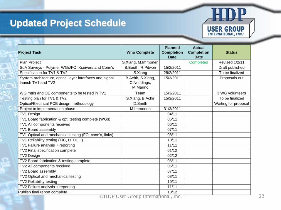
Updated Project Schedule
22 ©HDP User Group International, Inc.
Project Task Who Complete
Planned
Completion
Date
Actual
Completion
Date
Status
Plan Project S.Xiang, M.Immonen Completed Revised 1/2/11
SoA Surveys - Polymer WGs/FO; Xceivers and Conn's B.Booth, R.Pitwon 15/2/2011 Draft published
Specification for TV1 & TV2 S.Xiang 28/2/2011 To be finalized
System architecture, optical layer interfaces and signal
launch TV1 and TV2
B.Achir, S.Xiang,
C.Noddings,
M.Marino
15/3/2011 Proposals out
WG mtrls and OE components to be tested in TV1 Team 15/3/2011 3 WG volunteers
Testing plan for TV1 & TV2 S.Xiang, B.Achir 15/3/2011 To be finalized
Optical/Electrical PCB design methodology D.Smith Waiting for proposal
Project to implementation phase M.Immonen 31/3/2011
TV1 Design 04/11
TV1 Board fabrication & opt. testing complete (WGs) 06/11
TV1 All components received 06/11
TV1 Board assembly 07/11
TV1 Optical and mechanical testing (FO, conn’s, links) 08/11
TV1 Reliability testing (T/C, HTOL,..) 10/11
TV1 Failure analysis + reporting 11/11
TV2 Final specification complete 01/12
TV2 Design 02/12
TV2 Board fabrication & testing complete 06/11
TV2 All components received 06/11
TV2 Board assembly 07/11
TV2 Optical and mechanical testing 08/11
TV2 Reliability testing 10/11
TV2 Failure analysis + reporting 11/11
Publish final report complete 10/12

Next Actions
• Finalize testing plan for TV1 (method, specific conditions)
• Finalize design specification and design features required
for TV1
• Agree board construction, materials (laminates, etc.),
optical components and connectors for TV1
• Identify resources (board design, fabrication, testing
sourcing CC) for TV1
• Commitments of team members
• Project to move into implementation
©HDP User Group International, Inc. 23

Interested Participants
©HDP User Group International, Inc. 24
Mailing lists status 09’10
– Fujitsu AT
– Hitachi
– Huawei
– IBM
– Isola Group
– Iteq
– ITRI
– Juniper
– TTM Meadville
– MMM
– Mayo Clinic
– Molex
– National Semic.
– Northrop Grumman
– Nokia Siemens
Network
– Optical Interlinks
– Oracle
– Park Electro
– Promex
– Purdue
– Reflex Photonics
– Rogers Corp
– Uta
– Wistron
– Xyratex
– Adamant
– Albemarle
– Alcatel-Lucent
– Atotech
– Boeing
– Celestica
– Cisco
– Conpart
– Dow
– Ericsson
– Flextronics
Contacts
©HDP User Group International, Inc.
Proprietary
25
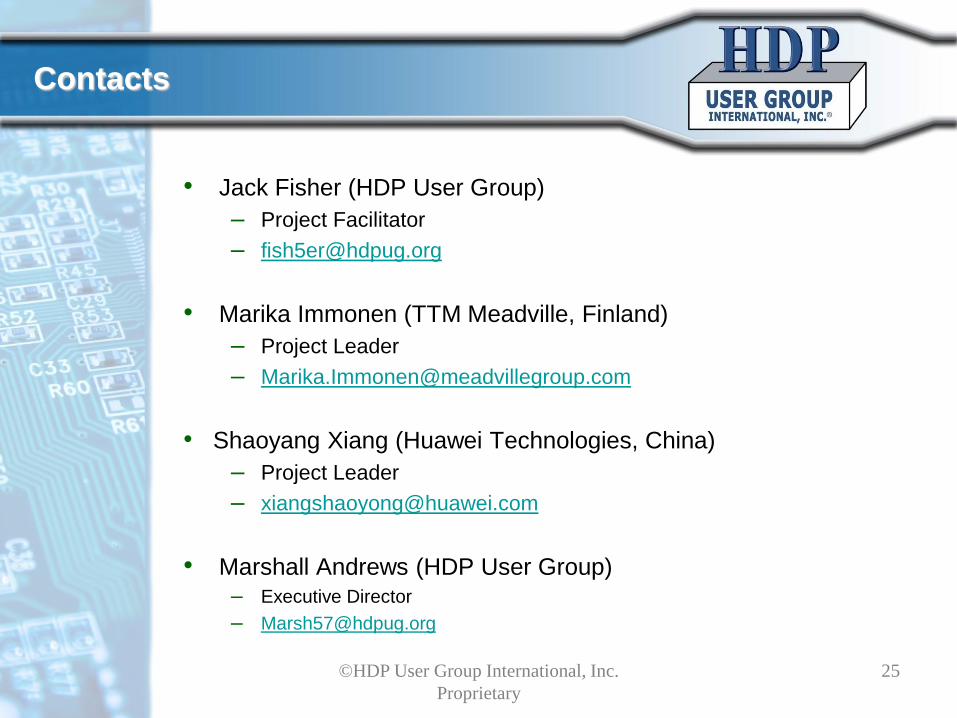
• Jack Fisher (HDP User Group)
– Project Facilitator
• Marika Immonen (TTM Meadville, Finland)
– Project Leader
• Shaoyang Xiang (Huawei Technologies, China)
– Project Leader
• Marshall Andrews (HDP User Group) – Executive Director

Back up
©HDP User Group International, Inc. 26

Standardization Initiatives
27 Source: IEC 62658 Ed 1.0 Standardization Roadmap of
Optical Circuit Boards and Related Packaging Technologies
• IEC 62496, 62658, 62661 • IEC 62496-1 Optical Circuit Boards (12/08); 8 standards on performance,
measurements, interface and optical backplanes, and products specification as drafts
• De Facto Standards in Japan • 19 de-facto standards on optical circuit boards, optical backplanes, optical
connectors and optical modules on board (JPCA, Japan Electronics Packaging and
Circuits Association)
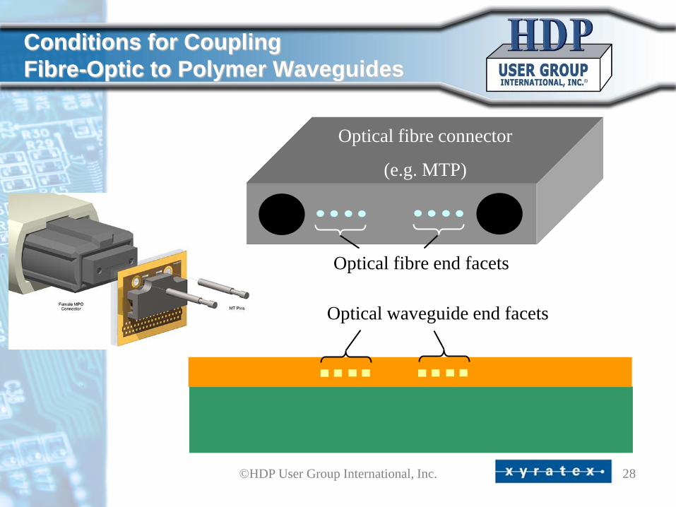
Conditions for Coupling
Fibre-Optic to Polymer Waveguides
©HDP User Group International, Inc. 28
Optical fibre connector
(e.g. MTP)
Optical fibre end facets
Optical waveguide end facets

Conditions for Coupling
Fibre-Optic to Polymer Waveguides
©HDP User Group International, Inc. 29
Input
waveguides
Output
waveguides
Fibre to polymer waveguide
1. Output Fibre N.A. ≤ (smaller or equal to)
Input Polymer WG N.A.
N.A. of conventional fibre ~ 0.2
N.A. of polymer waveguide ~ 0.25-0.3
2. Fibre Ø ≤ Waveguide Ø
Fibre core should fit
completely into
waveguide core
Polymer waveguide to fibre 3. Output Polymer WG N.A.
≤ Input Fibre N.A.
Acceptance
angles Acceptance
angles
4. Waveguide Ø <= Fibre Ø
Waveguide core
should fit completely
into fibre core
Input
waveguides
Output
Fibre
Output
waveguides
Input
Fibre
N.A. fibre ~ 0.2 < N.A. PWG ~ 0.3
NA condition not met NA condition qualified
Light Light

Example of FO/WG Interface
• Optical connector
(waveguide/Fiber)
must apply separate
design rules for in/out
channels
• Same applies for fiber-
ended transceivers
• Non-standard fibers
are used only for intra-
system links =>
external I/Os not
affected
©HDP User Group International, Inc. 30
Input
waveguides
Output
waveguides
Typical polymer waveguides
N.A. = 0.3
Core size = 50 μm x 50 μm
Output fibres
Low N.A. (e.g. 0.2)
Small core (e.g. 50 μm)
Standard 50/125 GI MMF
Input fibres
High N.A. (≥ 0.3)
Large core (≥ 71 μm)
Special fiber
Top Related