


Languages
Pages
Legal


Modeling of an interface between two solids
Ashcroft and Mermin Ch. 18Sze Ch.3
1987 Review Chapter by Tersoff

The Work Function of a Metal
A. If there are no interface dipoles• Negative value of Ef reflects the attractive
force of the positive ions

The Work Function of a Metal
B. Surface dipole – additional component due to dipole field
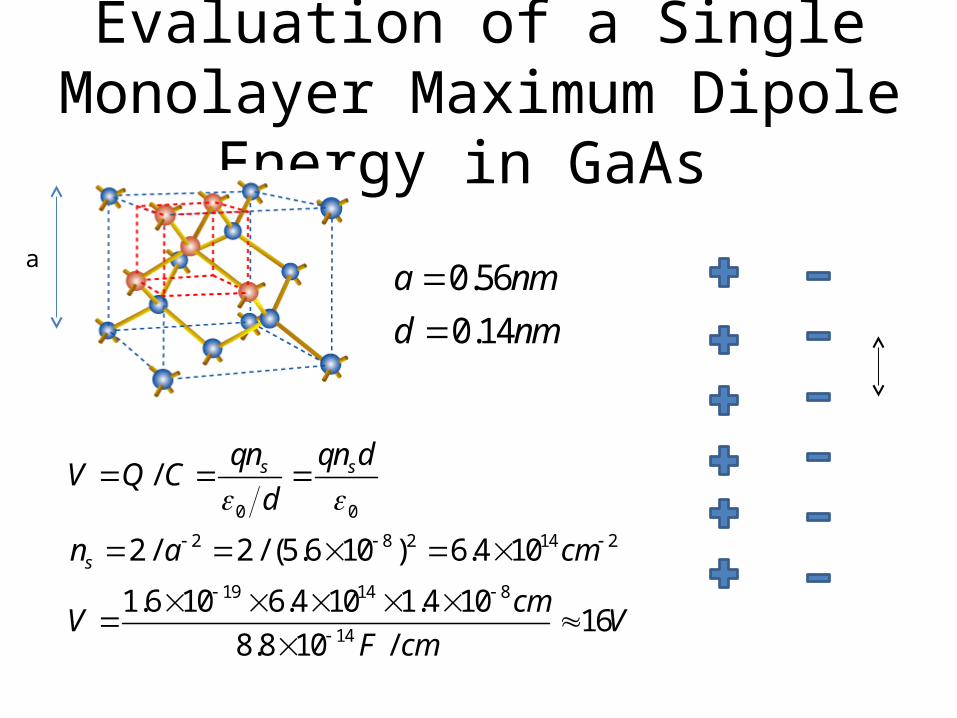
Evaluation of a Single Monolayer Maximum Dipole Energy in GaAs
0 0
2 8 2 14 2
19 14 8
14
/
2 / 2 / (5.6 10 ) 6.4 10
1.6 10 6.4 10 1.4 1016
8.8 10 /
s s
s
qn qn dV Q C
d
n a cm
cmV V
F cm
0.56
0.14
a nm
d nm
a

Two metals
• Same chemical potential after contact is established – if electrons are free, by the definition of chemical potential.
1 2 1 2( )q V V W W
2W1W
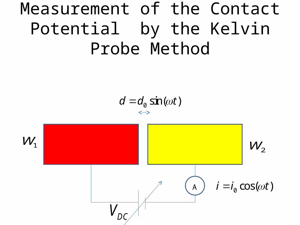
Measurement of the Contact Potential by the Kelvin Probe Method
2W1W
A
0 sin( )d d t
0 cos( )i i t
DCV

Ideal Insulator ε=1
• No charge redistribution due to an electric field – no dipole at the interface. Afinity rule exact
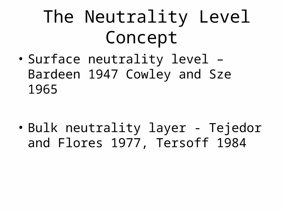
The Neutrality Level Concept
• Surface neutrality level – Bardeen 1947 Cowley and Sze 1965
• Bulk neutrality layer - Tejedor and Flores 1977, Tersoff 1984

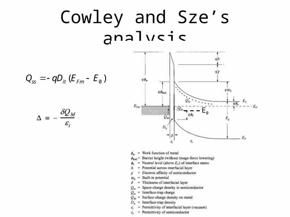
Cowley and Sze’s analysis
0( )ss it FmQ qD E E
E0

Cowley and Sze’s analysis
E0

Silicon Barrier with Metals
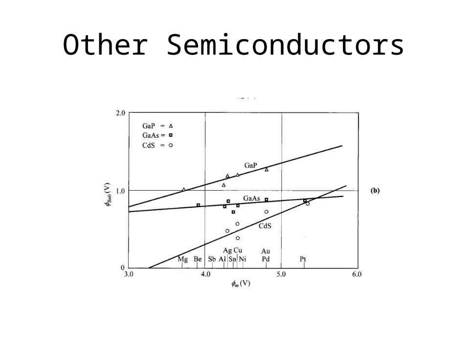
Other Semiconductors

Summary

The bulk neutrality level
• Epitaxial interfaces are almost defect free• Yet, the affinity rule is not obeyed• The bulk neutrality level plays a role
analogous to the Fermi level in metals• No Charge transfer if both neutrality layers
coincide
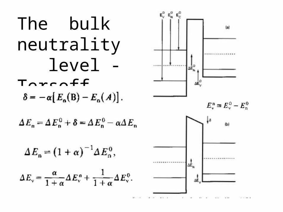
The bulk neutrality level -Tersoff

limits
metal
Ideal insulator
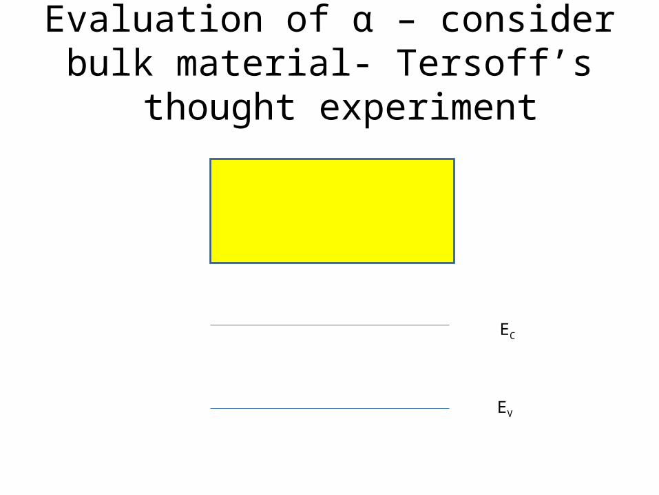
Evaluation of α – consider bulk material- Tersoff’s thought experiment
EC
EV

freeze all charges - introduce dipole –
EC
EV
ΔE 0
0 0 0 0n C VE E E E
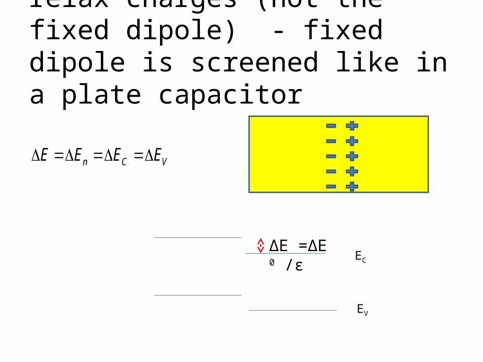
relax charges (not the fixed dipole) - fixed dipole is screened like in a plate capacitor
EC
EV
ΔE =ΔE 0 /ε
n C VE E E E

Compare to previous definitions
EC
EV
ΔE =ΔE 0 /ε
hence

Conclusion: in semiconductors neutrality levels are almost aligned

Microscopic origin of the dipole (the homogenous material thought
experiment)• States induced by tunneling – empty states are positively
charged, filled states negatively charged.
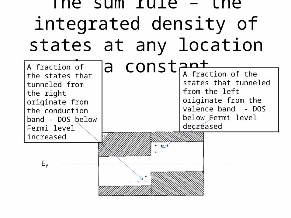
The sum rule – the integrated density of states at any location is
a constant
Ef
A fraction of the states that tunneled from the right originate from the conduction band – DOS below Fermi level increased
A fraction of the states that tunneled from the left originate from the valence band - DOS below Fermi level decreased

A heterojunction aligned at the - neutrality levels - total DOS bellow
Fermi level remains unchanged
Ef
A fraction of the states that tunneled from the left originate from the valence band
A fraction of the states that tunneled from the left originate from the conduction band

Microscopic or macroscopic α ?
• Tersoff – • but charge is located at bond distance• Tejedor and Flores calculate
1 r
2.5

Calculation of neutrality level at 1D (Tersoff)
Eb is a natural division between the valence and conduction bands
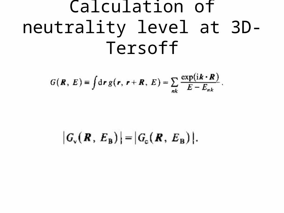
Calculation of neutrality level at 3D- Tersoff

Calculation of the neutrality level by Tersoff and comparison with
barrier height


2011 comments by Tersoff
A. I can't really say that my ideas have evolved much since then, since I moved on to other things. I don't remember what is in that chapter, but strictly speaking, both the interfacial properties and the bulk properties do matter. A metal-metal interface is the ideal example where bulk properties totally screen out interfacial effects. The smaller the dielectric constant, the more the interfacial details matter. The interface could also dominate if it is too non-bulk-like, e.g. non-stochiometric, or high density of defects.
Q. I am accustomed to the way of thinking which relates band alignment between semiconductors as well as Schottky barriers to the properties of the interface. Thinking of bulk properties in this context is unusual to me, and I was intrigued to find out how your
ideas have evolved over the years .

2011 comments by Tersoff
Just from my very out-of-date memories, I don't remember silicides behaving any differently than other metals -- i.e. Schottky barriers roughly consistent with calculated neutrality levels, with small shifts reflecting the different metal workfunctions.
There is much more opportunity for complications at III-V interfaces, especially for polar orientations like 001 and 111, because the chemistry might lead to a dipole at the interface, just as for polar surfaces. It's intriguing that such effects usually don't seem important -- different metals on (001) surfaces of III-V's show the trends expected from simple bulk arguments. This is convenient, but it isn't really understood.
Top Related