


Languages
Pages
Legal

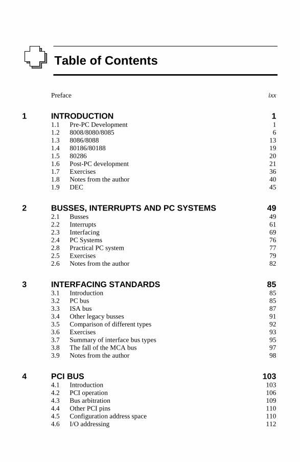
Table of Contents
Preface ixx
1 INTRODUCTION 1 1.1 Pre-PC Development 1 1.2 8008/8080/8085 6 1.3 8086/8088 13 1.4 80186/80188 19 1.5 80286 20 1.6 Post-PC development 21 1.7 Exercises 36 1.8 Notes from the author 40 1.9 DEC 45
2 BUSSES, INTERRUPTS AND PC SYSTEMS 49 2.1 Busses 49 2.2 Interrupts 61 2.3 Interfacing 69 2.4 PC Systems 76 2.8 Practical PC system 77 2.5 Exercises 79 2.6 Notes from the author 82
3 INTERFACING STANDARDS 85 3.1 Introduction 85 3.2 PC bus 85 3.3 ISA bus 87 3.4 Other legacy busses 91 3.5 Comparison of different types 92 3.6 Exercises 93 3.7 Summary of interface bus types 95 3.8 The fall of the MCA bus 97 3.9 Notes from the author 98
4 PCI BUS 103 4.1 Introduction 103 4.2 PCI operation 106 4.3 Bus arbitration 109 4.4 Other PCI pins 110 4.5 Configuration address space 110 4.6 I/O addressing 112

Table of contents xi
4.7 Exercises 116 4.8 Example manufacturer and plug-and-play IDs 118 4.9 Notes from the author 119
5 MOTHERBOARD DESIGN 121 5.1 Introduction 121 5.2 TX motherboard 132 5.3 Exercises 136 5.4 Notes from the author 137
6 IDE AND MASS STORAGE 139 6.1 Introduction 139 6.2 Tracks and sectors 139 6.3 Floppy disks 140 6.4 Fixed disks 141 6.5 Drive specifications 142 6.6 Hard disk and CD-ROM interfaces 142 6.7 IDE interface 143 6.8 IDE communication 144 6.9 Optical storage 150 6.10 Magnetic tape 153 6.11 Exercises 155 6.12 Notes from the author 156
7 SCSI 157 7.1 Introduction 157 7.2 SCSI types 157 7.3 SCSI interface 159 7.4 SCSI operation 162 7.5 SCSI pointers 164 7.6 Message system description 165 7.7 SCSI commands 167 7.8 Status 169 7.9 Exercises 171 7.10 Notes from the author 172
8 PCMCIA 173 8.1 Introduction 173 8.2 PCMCIA signals 173 8.3 PCMCIA registers 175 8.4 Exercises 179 8.5 Notes from the author 179
9 USB AND FIREWIRE 181 9.1 Introduction 181

xii Computer busses
9.2 USB 182 9.3 Firewire 186 9.4 Exercises 190 9.5 Notes from the author 190
10 GAMES PORT, KEYBOARD AND MOUSE 191 10.1 Introduction 191 10.2 Games port 191 10.3 Keyboard 195 10.4 Mouse and keyboard interface 198 10.5 Mouse 199 10.6 Exercises 200 10.7 Notes from the author 201
11 AGP 203 11.1 Introduction 203 11.2 PCI and AGP 204 11.3 Bus transactions 205 11.4 Pin description 205 11.5 AGP master configuration 208 11.6 Bus commands 209 11.7 Addressing modes and bus operations 210 11.8 Register description 210 11.9 Exercises 215 11.10 Notes from the author 215
12 FIBRE CHANNEL 217 12.1 Introduction 217 12.2 Comparison 217 12.3 Fibre channel standards 218 12.4 Cables, hubs, adapters and connectors 219 12.5 Storage Devices and storage area networks 221 12.6 Networks 221 12.7 Exercises 222 12.8 Notes from the author 222
13 RS-232 223 13.1 Introduction 223 13.2 Electrical characteristics 223 13.3 Communications between two nodes 228 13.4 Programming RS-232 233 13.5 RS-232 programs 237 13.6 Exercises 241 13.7 Notes from the author 246

Table of contents xiii
14 RS-422, RS-423 AND RS-485 247 14.1 Introduction 247 14.2 RS-485 (ISO 8482) 247 14.3 Line drivers 249 14.4 RS-232/485 converter 250 14.5 Exercises 251 14.6 Note from the author 251
15 MODEMS 253 15.1 Introduction 253 15.2 RS-232 communications 254 15.3 Modem standards 255 15.4 Modem commands 256 15.5 Modem set-ups 258 15.6 Modem indicator 260 15.7 Profile viewing 260 15.8 Test modes 261 15.9 Digital modulation 264 15.10 Typical modems 265 15.11 Fax transmission 267 15.12 Exercises 268 15.13 Notes from the author 269
16 PARALLEL PORT 271 16.1 Introduction 271 16.2 PC connections 271 16.3 Data handshaking 272 16.4 I/O addressing 275 16.5 Interrupt-driven parallel port 279 16.6 Exercises 284 16.7 Notes from the author 287
17 ENHANCED PARALLEL PORT 289 17.1 Introduction 289 17.2 Compatibility mode 289 17.3 Nibble mode 290 17.4 Byte mode 293 17.5 EPP 294 17.6 ECP 296 17.7 Exercises 300 17.8 Note from the author 300
18 MODBUS 301 18.1 Modbus protocol 301 18.2 Function codes 307
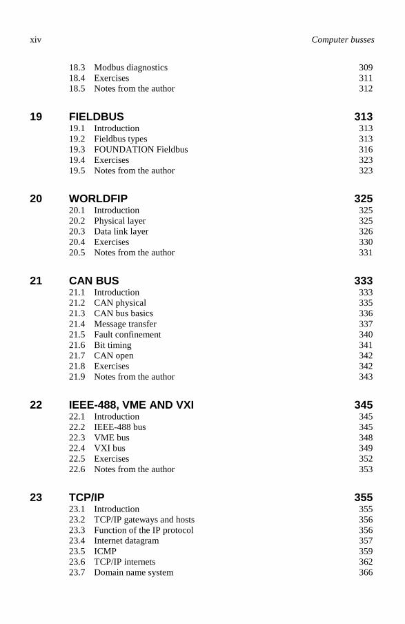
xiv Computer busses
18.3 Modbus diagnostics 309 18.4 Exercises 311 18.5 Notes from the author 312
19 FIELDBUS 313 19.1 Introduction 313 19.2 Fieldbus types 313 19.3 FOUNDATION Fieldbus 316 19.4 Exercises 323 19.5 Notes from the author 323
20 WORLDFIP 325 20.1 Introduction 325 20.2 Physical layer 325 20.3 Data link layer 326 20.4 Exercises 330 20.5 Notes from the author 331
21 CAN BUS 333 21.1 Introduction 333 21.2 CAN physical 335 21.3 CAN bus basics 336 21.4 Message transfer 337 21.5 Fault confinement 340 21.6 Bit timing 341 21.7 CAN open 342 21.8 Exercises 342 21.9 Notes from the author 343
22 IEEE-488, VME AND VXI 345 22.1 Introduction 345 22.2 IEEE-488 bus 345 22.3 VME bus 348 22.4 VXI bus 349 22.5 Exercises 352 22.6 Notes from the author 353
23 TCP/IP 355 23.1 Introduction 355 23.2 TCP/IP gateways and hosts 356 23.3 Function of the IP protocol 356 23.4 Internet datagram 357 23.5 ICMP 359 23.6 TCP/IP internets 362 23.7 Domain name system 366
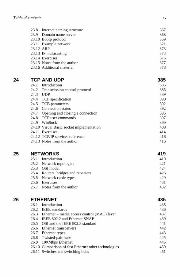
Table of contents xv
23.8 Internet naming structure 367 23.9 Domain name server 368 23.10 Bootp protocol 369 23.11 Example network 371 23.12 ARP 373 23.13 IP multicasting 373 23.14 Exercises 375 23.15 Notes from the author 377 23.16 Additional material 378
24 TCP AND UDP 385 24.1 Introduction 385 24.2 Transmission control protocol 385 24.3 UDP 389 24.4 TCP specification 390 24.5 TCB parameters 392 24.6 Connection states 392 24.7 Opening and closing a connection 395 24.8 TCP user commands 397 24.9 WinSock 399 24.10 Visual Basic socket implementation 408 24.11 Exercises 414 24.12 TCP/IP services reference 416 24.13 Notes from the author 416
25 NETWORKS 419 25.1 Introduction 419 25.2 Network topologies 421 25.3 OSI model 424 25.4 Routers, bridges and repeaters 426 25.5 Network cable types 429 25.6 Exercises 431 25.7 Notes from the author 432
26 ETHERNET 435 26.1 Introduction 435 26.2 IEEE standards 436 26.3 Ethernet – media access control (MAC) layer 437 26.4 IEEE 802.2 and Ethernet SNAP 439 26.5 OSI and the IEEE 802.3 standard 441 26.6 Ethernet transceivers 442 26.7 Ethernet types 443 26.8 Twisted-pair hubs 445 26.9 100 Mbps Ethernet 445 26.10 Comparison of fast Ethernet other technologies 450 26.11 Switches and switching hubs 451

xvi Computer busses
26.12 Network interface card design 453 26.13 Gigabit Ethernet 457 26.14 Exercises 462 26.15 Ethernet crossover connections 464 26.16 Notes from the author 465
27 RS-232 PROGRAMMING USING VISUAL BASIC 467 27.1 Introduction 467 27.2 Properties 467 27.3 Events 473 27.4 Example program 474 27.5 Error messages 475 27.6 RS-232 polling 476 27.7 Exercises 477
28 INTERRUPT-DRIVEN RS-232 479 28.1 Interrupt-driven RS-232 479 28.2 DOS-based RS-232 program 479 28.3 Exercises 486
A PC PROCESSORS 489 A.1 Introduction 489 A.2 8086/88 490 A.3 80386/80486 495 A.4 Pentium/Pentium Pro 501 A.5 Exercises 505
B VESA VL-LOCAL BUS 509
C MODEM CODES 511 C.1 AT commands 511 C.2 Result codes 513 C.3 S-registers 514
D REDUNDANCY CHECKING 519 D.1 Cyclic redundancy check (CRC) 519 D.2 Longitudinal/vertical redundancy checks (LRC/VRC) 523
E ASCII CHARACTER CODE 525 E.1 Standard ASCII 525 E.2 Extended ASCII code 527
Table of contents xvii
F QUICK REFERENCE 529 F.1 Notes from the author 531
G ISDN 533 G.1 Introduction 533 G.2 ISDN channels 534 G.3 ISDN physical layer interfacing 535 G.4 ISDN data link layer 538 G.5 ISDN network layer 541 G.6 Speech sampling 543 G.7 Exercises 544
H MICROSOFT WINDOWS 547 H.1 Introduction 547 H.2 Windows registry 548 H.3 Device drivers 550 H.4 Configuration manager 551 H.5 Virtual machine manager (VMM) 552 H.6 Multiple file systems 555 H.7 Core system components 557 H.8 Multitasking and threading 559 H.9 Plug-and-play process 561 H.10 Windows NT architecture 561 H.11 Windows 95 and Windows 98 564 H.12 Fundamentals of Operating Systems 565 H.13 Exercises 567
I HDLC 569 I.1 Introduction 569 I.2 HDLC protocol 570 I.3 Transparency 574 I.4 Flow control 574 I.5 Derivatives of HDLC 576
J EXAMPLE WINSOCK CODE FOR VISUAL BASIC J.1 My client (myClient.frm) 579 J.2 My server (myServer.frm) 583 J.3 Choice form (ChoiceSC.frm) 586 J.4 Error panel (ErrorPanel.frm) 587 J.5 Help form (help.frm) 589
Index 591

xviii Computer busses

xix
Preface What is it that really determines the performance of a computer? Is it the processor? No, not really. It is the amount of memory that it has? No, not really. Is it the speed of the disk drives? No, not really. This is because computers can have a fast processor, and lots of memory, and a fast disk drive, but they do not count for much if the busses that con-nect them to each other do not operate efficiently. The performance of a computer thus directly relates to the busses that connect it. The computer bus is thus the foundation of the modern computer. Without them, a computer would just be a bundle of components. Busses provide the mechanism for the orderly flow of data over the required chan-nel. They range vastly in their specification. From busses that transmit hundreds of mil-lions of bytes every second (such as with the PCI bus) to busses which transmit only a few thousand bytes per second (such as with the RS-232 bus). They vary in their speci-fication as no one bus can provide the required specification for all applications. For example, graphics adaptors and electronic memory require high data throughputs, and must thus be closely coupled to the processor (known as a local bus connection), whereas modems and printers require relatively slow transfer rates, and must be coupled to a bus which does not try and hog the processor for long periods. The perfect bus system would use a single connector for every device that connects to it, would be able to sense and configure whichever devices connected to it, would be able to use any type of cable, and devices which connect to it would simply require a tap from one connection onto the next (a daisy-chain connection). It would support high data transfer devices, alongside low data transfer devices, but the low data transfer de-vices would not hog the bus in favour of the high data transfer devices. It would support real-time data (such as speech and audio) and non-real-time data (such as computer data) in an integrated way, so that the non-real-time data would not swamp the real-time data. This bus, of course, does not exist, or if it does exist, it will be too expensive, and would be incompatible with all the existing busses. Thus, we have many different types of busses, each with their own application. It is impossible to immediately change com-puter systems every time a new application comes along. We do not immediately knock down our house every time we want to upgrade it. This would be expensive, and we probably would be able to sell it after we had done it. We thus try to use our existing framework and integrate with it. Internal busses connect the processor to its memory and its interface busses (such as the PCI and the ISA busses). The external busses allow the connection the external de-vices to the computer, in an orderly manner. The book splits into five main areas, these are: 1. PC Interfaces.
• Introduction • PC Interfacing. • Interfacing Standards
2. Local busses. • PC/ISA.

xx Computer busses
• PCI/AGP. • Motherboard Design • USB. • Games Port, Keyboard and Mouse. • Fibre Channel. • RS-232/RS-422/Modems. • Parallel Port.
3. Instrumentation busses. • Modbus. • Fieldbus. • WorldFIP. • CAN bus. • IEEE-488. • VME/VXI.
4. Network busses. • Ethernet. • ISDN/HDLC. • Protocols (TCP/IP).
5. Bus programming/protocols • TCP/IP. • RS-232. • Parallel port.
Slides and backup information can be found on my WWW site at: http://www.dcs.napier.ac.uk/~bill/books.html Questions and any feedback that you have on the book should be sent to: [email protected] or [email protected] I have included some notes at the end of most of the chapters which are much lighter in content than the main text. These are my own options, and, of course, should not be taken as fact. In fact they are there for debate, and in some cases your may disagree with some of my comments. For example, I think that the TCP and IP protocols have done more for the freedom of speech, and world peace than all of the diplomats around the world, put together. They have no respect for borders, they do not favour any lan-guage, and they do not mind what the data is, and on what computer it came from. They are truly making the world into a village. Before I start on this book, I must reveal a little secret. My favourite bus, apart from the Number 45 bus which takes me to work every day, is the RS-232 bus. It’s not be-cause it is the most technological advanced bus, or that it is easy to interface. Its be-cause I grew an excellent consultancy company by writing program for it. So, I’ve got a soft spot for RS-232. Long may it reign.

1
Introduction
1.1 Pre-PC Development
One of the first occurrences of computer technology occurred in the USA in the 1880s. It was due to the American Constitution demanding that a survey is undertaken every 10 years. As the population in the USA increased, it took an increasing amount of time to produce the statistics. By the 1880s, it looked likely that the 1880 survey would not be complete until 1890. To overcome this, Herman Hollerith (who worked for the Government) devised a ma-chine which accepted punch cards with information on them. These cards allowed a current to pass through a hole when there was a hole present. Hollerith’s electromechanical machine was extremely successful and used in the 1890 and 1900 Censuses. He even founded the company that would later become International Business Machines (IBM): CTR (Computer Tabulating Recording). Unfortunately, Hol-lerith’s business fell into financial difficulties and was saved by a young salesman at CTR, named Tom Watson, who recognized the potential of selling punch card-based calculating machines to American business. He eventually took over the company Watson, and, in the 1920s, he renamed it International Business Machines Corporation (IBM). After this, elec-tromechanical machines were speeded up and improved. Electromechnical computers would soon lead to electronic computers, using valves. The first electronic computers were developed, independently, in 1943; these were the ‘Harvard Mk I’ and Colossus. Colossus was developed in the UK and was used to crack the German coding system (Lorenz cipher), whereas ‘Harvard Mk I’ was developed at Harvard University and was a general-purpose electromechanical programmable computer. These led to the first generation of computers which used electronic valves and used punched cards for their main, non-volatile storage. The world’s first large electronic computer (1946), containing 19 000 values was built at the University of Pennsylvania by John Eckert during World War II. It was called ENIAC (Electronic Numerical Integrator and Computer) and it ceased operation in 1957. By today’s standards, it was a lumbering dinosaur and by the time it was dismantled it weighed over 30 tons and spread itself over 1500 square feet. Amazingly, it also consumed over 25 kW of electrical power (equivalent to the power of over 400, 60 W light bulbs), but could perform over 100 000 calculations per second (which is reasonable, even by today’s standards). Un-fortunately, it was unreliable, and would only work for a few hours, on average, before a valve needed to be replaced. Faultfinding, though, was easier in those days, as a valve, which was working, would not glow, and would be cold to touch. Valves were fine and were used in many applications, such as in TV sets and radios, but they were unreliable and consumed great amounts of electrical power, mainly to the heating element on the cathode. By the 1940s, several scientists at the Bell Laboratories were inves-tigating materials called semiconductors, such as silicon and germanium. These substances only conducted electricity moderately well, but when they where doped with impurities their
1

2 Introduction
resistance changed. From this work, they made a crystal called a diode, which worked like a valve, but had many advantages, including the fact that it did not require a vacuum and was much smaller. It also worked well at room temperatures, required little electrical current and had no warm-up time. This was the start of microelectronics. One of the great revolutions of all time occurred on December 1948 when William Shockley, Walter Brattain, and John Bardeen at the Bell Labs produced a transistor that could act as a triode. It was made from a germanium crystal with a thin p-type section sand-wiched between two n-type materials. Rather than release its details to the world, Bell Laboratories kept its invention secret for over seven months so that they could fully under-stand its operation. They soon applied for a patent for the transistor and, on 30 June 1948, they finally revealed the transistor to the world. Unfortunately, as with many other great in-ventions, it received little public attention and even less press coverage (the New York Times gave it 4½ inches on page 46). It must be said that few men have made such a profound change on the world, and Shockley, Brattain, and Bardeen were deservedly awarded the No-bel Prize in 1956. To commercialize on his success, Shockley, in 1955, founded Shockley Semiconductor. Then in 1957, eight engineers decided they could not work within Shockley Semiconductor and formed Fairchild Semiconductors, which would become one of the most inventive companies in Silicon Valley. Unfortunately, most of the time Fairchild Semicon-ductors did not fully exploit its developments, and was more of an incubator for many of the innovators in the electronics industry. Around the same time, Kenneth Olsen founded the Digital Equipment Corporation (DEC), who would go on to become one of the key compa-nies in the computer industry, along with IBM. Previously, in 1952, GW Dummer, a radar expert from Britain’s Royal Radar Establish-ment had presented a paper proposing that a solid block of materials could be used to con-nect electronic components, without connecting wires. This would lay the foundation of the integrated circuit. Transistors were initially made from germanium, which is not a robust material and can-not withstand high temperatures. The first company to propose the use of silicon transistors was a geological research company named Texas Instruments (which had diversified into transistors). Then, in May 1954, Texas Instruments started commercial production of silicon transistors. Soon many companies were producing silicon transistors and, by 1955, the elec-tronic valve market had peaked, while the market for transistors was rocketing. The larger electronic valve manufacturers, such as Western Electric, CBS, Raytheon and Westinghouse failed to adapt to the changing market and quickly lost their market share to the new transis-tor manufacturing companies, such as Texas Instruments, Motorola, Hughes and RCA. In July 1958, at Texas Instruments, Jack St. Clair Kilby proposed the creation of a mono-lithic device (an integrated circuit) on a single piece of silicon. Then, in September, he pro-duced the first integrated circuit, containing five components on a piece of germanium that was half an inch long and was thinner than a toothpick. The following year, Fairchild Semiconductor filed for a patent for the planar process of manufacturing transistors. This process made commercial production of transistors possible and led to Fairchild’s introduction, in two years, of the first commercial integrated circuit. Within a few years, transistors were small enough to make hearing aids that fitted into the ear, and soon within pacemakers. Companies, such as Sony, started to make transistors oper-ate over higher frequencies and within larger temperature ranges. Eventually they became so small that many of them could be placed on a single piece of silicon. These were referred to as microchips and they started the microelectronics industry. The first two companies who developed the integrated circuit, were Texas Instruments and Fairchild Semiconductor. At Fairchild Semiconductor, Robert Noyce constructed an integrated circuit with components

Computer busses 3
connected by aluminium lines on a silicon-oxide surface layer on a plane of silicon. He then went on to lead one of the most innovate companies in the world, the Intel Corporation. After ENIAC, progress was fast in the computer industry and, by 1948, small electronic computers were being produced in quantity within five years (2000 were in use), in 1961 it was 10 000, 1970 100 000. IBM, at the time, had a considerable share of the computer mar-ket. So much so that a complaint was filed against them alleging monopolistic practices in its computer business, in violation of the Sherman Act. By January 1954, the US District Court made a final judgment on the complaint against IBM. For this, a ‘consent decree’ was then signed by IBM, which placed limitations on how IBM conducts business with respect to ‘electronic data processing machines’. In 1954, the IBM 650 was built and was considered the workhorse of the industry at the time (which sold about 1000 machines, and used valves). In November 1956, IBM showed how innovative they were by developing the first hard disk, the RAMAC 305. It was tower-ing by today’s standards, with 50 two-foot diameter platters, giving a total capacity of 5 MB. Around the same time, the Massachusetts Institute of Technology produced the first transis-torised computer: the TX-O (Transistorized Experimental computer). Seeing the potential of the transistor, IBM quickly switched from valves to transistors and, in 1959, they produced the first commercial transistorised computer. This was the IBM 7090/7094 series, and it dominated the computer market for years. Programs written on these mainframe computers were typically either machine code (us-ing the actual binary language that the computer understood) or using one of the new com-piled languages, such as COBOL and FORTRAN. FORTRAN was well suited to engineer-ing and science as it is based around mathematical formulas. COBOL was more suited to business applications. FORTRAN was developed in 1957 (typically known as FORTRAN 57) and considerably enhanced the development of computer programs, as the program could be writing in a near-English form, rather than using a binary language. With FORTRAN, the compiler converts the FORTRAN statements into a form that the computer can understand. At the time, FORTRAN programs were stored on punch cards, and loaded into a punch-card reader to be read into the computer. Each punch card had holes punched into them to repre-sent ASCII characters. Any changes to a program would require a new set of punch cards. In 1959, IBM built the first commercial transistorised computer named the IBM 7090/7094 series, which dominated the computer market for many years. In 1960, in New York, IBM went on to develop the first automatic mass-production facility for transistors. In 1963, the Digital Equipment Company (DEC) sold their first minicomputer, to Atomic En-ergy of Canada. DEC would become the main competitor to IBM, but eventually fail as they dismissed the growth in the personal computer market. The second generation of computers started in 1961 when the great innovator, Fairchild Semiconductor, released the first commercial integrated circuit. In the next two years, sig-nificant advances were made in the interfaces to computer systems. The first was by Teletype who produced the Model 33 keyboard and punched-tape terminal. It was a classic design and was on many of the available systems. The other advance was by Douglas Engelbart who received a patent for the mouse-pointing device for computers. The production of transistors increased, and each year brought a significant decrease in their size. Gordon Moore, in 1964, plotted the growth in the number of transistors that could be fitted onto a single microchip, and found that the number of transistors that can be fitted onto an integrated circuit approximately doubles every 18 months. This is now known as Moore’s law, and has been surprisingly accurate ever since. In 1964, Texas Instruments also received a patent for the integrated circuit. At the time, there were only three main ways of writing computer programs: machine

4 Introduction
code, FORTRAN or COBOL. These languages were often difficult for inexperienced users to use. So, in 1964, John Kemeny and Thomas Kurtz at Dartmouth College developed the BASIC (Beginners All-purpose Symbolic Instruction Code) programming language. It was a great success, although has never been used much in ‘serious’ applications, until Microsoft developed Visual BASIC, which used BASIC as a foundation language, but enhanced it with an excellent development system. Many of the first personal computers used BASIC as a standard programming language. The third generation of computers started in 1965 with the use of integrated circuits rather than discrete transistors. IBM again was innovative and created the System/360 main-frame. In the course of history, it was a true classic computer. Then, in 1970, IBM introduced the System/370, which included semiconductor memories. All of the computers were very expensive (approx. $1 000 000), and were the great computing workhorses of the time. Unfortunately, they were extremely expensive to purchase and maintain. Most companies had to lease their computer systems, as they could not afford to purchase them. As IBM happily clung to their mainframe market, several new companies were working away to erode their share. DEC would be the first, with their minicomputer, but it would be the PC companies of the future who would finally overtake them. The beginning of their loss of market share can be traced to the development of the microprocessor, and to one company: Intel. In 1967, though, IBM again showed their leadership in the computer industry by developing the first floppy disk. The growing electronics industry started to entice new companies to specialize in key areas, such as International Research who applied for a patent for a method of constructing double-sided magnetic tape utilizing a Mumetal foil inter layer. The beginning of the slide for IBM occurred in 1968, when Robert Noyce and Gordon Moore left Fairchild Semiconductors and met up with Andy Grove to found Intel Corpora-tion. To raise the required finance they went to a venture capitalist named Arthur Rock. He quickly found the required start-up finance, as Robert Noyce was well known for being the person who first put more than one transistor of a piece of silicon. At the same time, IBM scientist John Cocke and others completed a prototype scientific computer called the ACS, which used some RISC (Reduced Instruction Set Computer) con-cepts. Unfortunately, the project was cancelled because it was not compatible with the IBM’s System/360 computers. Several people were proposing the idea of a computer-on-a-chip, and International Re-search Corp. were the first to develop the required architecture, modelled on an enhanced DEC PDP-8/S concept. Wayne Pickette, at the time, proposed to Fairchild Semiconductor that they should develop a computer-on-a-chip, but was turned down. So, he went to work with IBM and went on to design the controller for Project Winchester, which had an en-closed flying-head disk drive. In the same year, Douglas C. Engelbart, of the Stanford Research Institute, demonstrated the concept of computer systems using a keyboard, a keypad, a mouse, and windows at the Joint Computer Conference in San Francisco’s Civic Center. He also demonstrated the use of a word processor, a hypertext system, and remote collaboration. His keyboard, mouse and windows concept has since become the standard user interface to computer systems. In 1969, Hewlett-Packard branched into the world of digital electronics with the world’s first desktop scientific calculator: the HP 9100A. At the time, the electronics industry was producing cheap pocket calculators, which led to the development of affordable computers, when the Japanese company Busicom commissioned Intel to produce a set of between eight and 12 ICs for a calculator. Then instead of designing a complete set of ICs, Ted Hoff, at Intel, designed an integrated circuit chip that could receive instructions, and perform simple integrated functions on data. The design became the 4004 microprocessor. Intel produced a

Computer busses 5
set of ICs, which could be programmed to perform different tasks. These were the first ever microprocessors and soon Intel (short for Integrated Electronics) produced a general-purpose 4-bit microprocessor, named the 4004. In April 1970, Wayne Pickette proposed to Intel that they use the computer-on-a-chip for the Busicom project. Then, in December, Gilbert Hyatt filed a patent application entitled ‘Single Chip Integrated Circuit Computer Architecture’, the first basic patent on the micro-processor. The 4004, as shown in Figure 1.1, caused a revolution in the electronics industry as pre-vious electronic systems had a fixed functionality. With this processor, the functionality could be programmed by software. Amazingly, by today’s standards, it could only handle four bits of data at a time (a nibble), contained 2000 transistors, had 46 instructions and al-lowed 4 KB of program code and 1 KB of data. From this humble start, the PC has since evolved using Intel microprocessors. Intel had previously been an innovative company, and had produced the first memory device (static RAM, which uses six transistors for each bit stored in memory), the first DRAM (dynamic memory, which uses only one transistor for each bit stored in memory) and the first EPROM (which allows data to be downloaded to a device, which is then permanently stored). In the same year, Intel announced the 1 KB RAM chip, which was a significant increase over previously produced memory chip. Around the same time, one of Intel’s major partners, and also, as history has shown, competitors, Advanced Micro Devices (AMD) Incorporated was founded. It was started when Jerry Sanders and seven others left – yes, you’ve guessed it, Fairchild Semiconductor. The incubator for the electronics industry was producing many spin-off companies. At the same time, the Xerox Corporation gathered a team at the Palo Alto Research Center (PARC) and gave them the objective of creating ‘the architecture of information.’ It would lead to many of the great developments of computing, including personal distributed computing, graphical user interfaces, the first commercial mouse, bit-mapped displays, Ethernet, client/server architecture, object-oriented programming, laser printing and many of the basic protocols of the Internet. Few research centers have ever been as creative, and forward thinking as PARC was over those years. In 1971, Gary Boone, of Texas Instruments, filed a patent application relating to a single-chip computer and the microprocessor was released in November. Also in the same year, Intel copied the 4004 micro-processor to Busicom. When released the basic specifi-cation of the 4004 was: • Data bus: 4-bit • Clock speed: 108 kHz • Price: $200 • Speed: 60 000 operations per second • Transistors: 2300
Figure 1.1 Intel 4004 die

6 Introduction
• Silicon: 10-micron technology, 3×4 mm2 • Addressable memory: 640 bytes Intel then developed an EPROM, which integrated into the 4004 to enhance development cycles of microprocessor products. Another significant event occurred when Bill Gates and Paul Allen, calling themselves the ‘Lakeside Programming Group’ signed an agreement with Computer Center Corporation to report bugs in PDP-10 software, in exchange for computer time. Other significant effects at the time were: • Ken Thompson, at AT&T’s Bell Laboratories, wrote the first version of the Unix operat-
ing system. • Gary Starkweather, at Xerox, used a laser beam along with the standard photocopying
processor to produce a laser printer. • The National Radio Institute introduced the first computer kit, for $503. • Texas Instruments develops the first microcomputer-on-a-chip, containing over 15 000
transistors. • IBM introduced the memory disk, or floppy disk, which was an 8-inch floppy plastic disk
coated with iron oxide. • Wang Laboratories introduced the Wang 1200 word processor system. • Niklaus Wirth invented the Pascal programming language. BASIC and FORTRAN had
long been known for producing unstructured programs, with lots of GOTOs and RE-TURNs. Pascal was intended to teach good, modular programming practices, but was quickly accepted for its clean, pseudocode-like language. Today it still survives, but has struggled against C/C++ (mainly because of the popularity of Unix) and Java (because of its integration with the Internet), but lives with Borland Delphi, an excellent Microsoft Windows development system.
1.2 8008/8080/8085
In 1974, Intel was a truly innovative company, and was the first to develop an 8-bit micro-processor. These devices could handle eight bits (a byte) of data at a time and were: • 8008 (0.2 MHz, 0.06 MIPS, 3500 transistors, 10-micron technology, 16 KB memory). • 8080 (2 MHz, 0.64 MIPS, 6000 transistors, 6-micron technology, 64 KB memory). • 8085 (5 MHz, 0.37 MIPS, 6500 transistors, 3-micron technology, 64 KB memory). These were much more powerful than the previous 4-bit devices and were used in many early microcomputers and in applications such as electronic instruments and printers. The 8008 had a 14-bit address bus and could thus address up to 16 KB of memory, and the 8080 and 8085 had 16-bit address busses, giving them limit of 64 KB. Table 1.1 outlines the basic specification for the main 8-bit microprocessors. At the time, Intel’s main product area was memory, and microprocessors seemed like a good way of increasing sales for other product lines, especially memory.

Computer busses 7
Table 1.1 Popular 8-bit microprocessors
Processor Release date (manufacturer)
Computer used in Example computers
8008 April 1972 (Intel) Mark-8 8080 April 1974 (Intel) Sol-20
MITS Altair 8800 IMSAI 8080
8085 March 1976 (Intel) Z80 Z80A
July 1976 (Zilog) Radio Shack TRS-80 Exidy Sorcerer Sinclair ZX81 Osborne 1 Xerox 820 DEC Rainbow 100 Sord M5/ M23P Sharp X1 Sony SMC-70
1. TRS-80 microcomputer, 4 KB RAM, 4 KB ROM, keyboard, black-and-white video display, and tape cassette, $600, Aug. 1977.
2. ZX81 (1 KB), $200, March 1981. ZX81 (2KB), $200. March 1981.
3. Osborne 1, 5-inch display, 64 KB RAM, keyboard, keypad, modem, and two 5.25-inch 100 KB disk drives, $17, April 1981.
6502/ 6502A
June 1976 (MOS Technologies)
Franklin Ace 1000 Atari 400/800 Commodore PET Apple II/III
1. Atari 400/800, 8 KB, $550/1000, Oct 1979. 2. PET 2001,4 KB RAM, 14 KB ROM, key-
board, display, and tape drive, $600. 3. Apple II, 4 KB RAM, 16 KB ROM, key-
board, 8-slot motherboard, game paddles, graphics/text interface to colour display (first ever), and built-in BASIC, $1300, April 1977.
4. Apple II Plus, 48 KB, June 1979. 5. Apple III, 5.25-inch floppy drive, $4500–
$8000, May 1980. 6. BBC Microcomputer System. 48 KB RAM,
73-key keyboard, and 16-colour graphics, Sept 1981.
6800/ 6809 1974 (Motorola) MITS Altair 680
1. TRS-80 Colour Computer, 4 KB RAM,
$400.
780-1 NEC 1. ZX80, 1 KB RAM and 4 KB ROM, $200, Feb. 1980.
Excited by the new 8-bit microprocessors, two kids from a private high school, Bill Gates and Paul Allen, rushed out to buy the new 8008 device (Figure 1.2). This they believed would be the beginning of the end of the large, and expensive, mainframes (such as the IBM range) and minicomputers (such as the DEC PDP range). They bought the processors for the high price of $360 (possibly, a joke at the expense of the IBM System/360 mainframe), but even they could not make it support BASIC programming. Instead, they formed the Traf-O-Data company and used the 8008 to analyse tickertape read-outs of cars passing in a street. The company would close down in the following year (1973) after it had made $20 000, but from this enterprising start, one of the leading computer companies in the world would grow: Microsoft (although it would initially be called Micro-soft).

8 Introduction
Intel knew that providing a processor alone would have very little impact on the market. It required a development system, which would allow industrial developers an easy method of developing hardware and software around the new processor. Thus, Intel introduced the Intellec 4 development system. The main competitors to the 8080 were: the Motorola 6800, the Zilog Z80 and the MOS Technology 6502. The Z80 had the advantage that it could run any programs written for the 8080, and, because it was also pin compatible, it could be easily swapped with the 8080 processor, without a change of socket. It also had many other advantages over the 8080, such as direct memory access, serial I/O technology, and full use of the ‘reserved’ op-codes (Intel had used only 246 out of the 256 available op-codes). The Z80 was also much cheaper than the 8080 and had a 2.5 MHz clock speed. After the release of the Z80, Intel produced a quick response: the 8085. This device fully used all the op-codes, but it was too late to
stop the tide towards Zilog. Many personal computers started to appear that were based on the Z80 processor, including the Radio Shack TRS-80, Osborne 1 and the Sinclair/Timex ZX81. The ZX81 caused a great revolution because of its cheapness, but unfortunately, most home users had to wait for many months to receive their kit, or for their prebuilt computer. However, as the computer was so original and cost effective, users were willing to wait for their prized system. Another great chal-lenger was the 6502, which was released in June 1975 and cost $25. This compared well with the 8080, which cost $150. It was used in many of the great personal computer systems, such as the Apple II (Fig-ure 1.3) and Atari 400.
For the first time, home users could actually build their own computer, and were avail-able from Altair and Mistral. With the success of the Z80, many companies were demanding to produce a second-source supply for the Z80 processors. The Motorola processor was also more powerful than the 8080. It was simpler in its design and only required a single 5 V supply, whereas the 8080 required three dif-ferent power supplies. At the end of the 1970s, IBM’s virtual monopoly on
Figure 1.4 ZX80
Figure 1.2 Intel 8008 die
Figure 1.3 Apple II computer

Computer busses 9
computer systems started to erode from the high-powered end as DEC developed their range of minicomputers and from the low-powered-end by companies developing computers based around the newly available 8-bit microprocessors, such as the 6502 and the Z80. IBM’s main contenders, other than DEC, were Apple and Commodore who introduced a new type of computer – the personal computer (PC). The leading systems, at the time, were the Apple I and the Commodore PET. These captured the interest of the home user and for the first time individuals had access to cheap computing power. These flagship computers spawned many others, such as the Sinclair ZX80/ZX81 (Figure 1.4), the BBC microcomputer, the Sinclair Spectrum, the Commodore Vic-20 and the classic Apple II (all of which where based on the 6502 or Z80). Most of these computers were aimed at the lower end of the market and were mainly used for playing games and not for business applications. IBM finally decided, with the advice of Bill Gates, to use the 8088 for its version of the PC, and not, as they had first thought, to use the 8080 device. Microsoft also persuaded IBM to introduce the IBM PC with a minimum of 64 KB RAM, instead of the 16 KB that IBM planned. Also, in 1972, at XEROX PARC, Alan Kay proposed that XEROX should build a port-able personal computer, called the Dynabook, which would be the size of an ordinary note-book; unfortunately, the PARC management did not support it. In future years, companies such as Toshiba and Compaq would fully exploit the idea. PARC eventually choose to de-velop the Alto personal computer. At the time, most people thought that personal computers would be used mainly as games computers. One of the major innovators in this was Atari, who were founded by Nolan Bushnell. They produced the first ever commercial game based on tennis, named Pong. By today’s standards, Pong used simple graphics. It had just two paddle lines, which could be moved left and right, and a square ball, which moved back and forward between the paddles. Atari and other companies would release many other classic games, such as Space Invaders, Asteroids and Frogger. At the time, Texas Instruments was well advanced in microprocessor development and introduced the TMS1000 one-chip microcomputer. It had 1 KB ROM, 32 bytes of RAM with a simple 4-bit processor. In the following year (1973), Intel filed a patent application for a memory system for a multichip digital computer. In 1973, the model for future computer systems occurred at Xerox’s PARC, when the Alto workstation was demonstrated with a bit mapped screen (showing the Cookie Monster, from Sesame Street). The following year, at Xerox, Bob Metcalfe demonstrated the Ethernet networking technology, which was destined to become the standard local area networking technique. It was far from perfect, as computers contended with each other for access to the network, but it was cheap and simple, and it worked relatively well. Also in 1973, before the widespread acceptance of PC-DOS, the future for personal com-puter operating systems looked to be CP/M (Control Program/Monitor), which was written by Gary Kildall of Digital Research. One of his first applications of CP/M was on the Intel 8008, and then on the Intel 8080. At the time, computers based on the 8008 started to appear, such as the Scelbi-8H, which cost $565 and had 1 KB of memory. IBM was also innovating at the time, creating a cheap floppy disk drive. They also pro-duced the IBM 3340 hard disk unit (a Winchester disk) which had a recording head which sat on a cushion of air, 18 millionths of an inch above the platter. The disk was made with four platters, each was 8-inches in diameter, giving a total capacity of 70 MB. A year later (1974), at IBM, John Cocke produced a high-reliability, low-maintenance computer called the ServiceFree. It was one of the first computers in the world to use RISC technology and it operated at the unbelievable speed of 80 MIPS. Most computers at the time were measured in a small fraction of a MIP, and, at the time, were over 50 times faster than

10 Introduction
IBM’s fastest mainframe. The project was eventually cancelled as a competing project named ‘Future Systems’ was consuming much of IBM’s resources. In the next year (1974), several personal computers began to appear, including the MITS-built (Micro Instrumentation and Telemetry Systems) computer based on Intel’s new 8080 device, at the cheap price of $500. It was released as the Altair 8800 microcomputer. One of the first prototypes for the Altair computer was lost, en-route, to New York, as it was to be reviewed and photographed for Popular Electronics. Eventually they did receive a new ver-sion and at a selling price of $439, it received great reviews. At PARC, the Bravo was developed for the Xerox Alto computer and demonstrated the first WYSIWYG (What You See Is What You Get) program for a personal computer. The Alto computer was then released onto the market. The following year Xerox demonstrated the Gypsy word-processing system, which was fully WYSIWYG. At Motorola, Chuck Ped-dle and Charlie Melear developed the 6800 microprocessor, which was never really success-ful in the personal computer market, but was used in many industrial and automotive applica-tions. While many of the processors at the time ran at 1 MHz or, at the most, 5 MHz, RCA re-leased the RISC-based 1802 processor, which ran at 6.4 MHz. It was used on a variety of systems, from video games to NASA space probes. Up to 1974, most programming languages had been produced either as a teaching lan-guage, such as Pascal or BASIC, or had been developed in the early days of computers, such as FORTRAN and COBOL. No software language had been developed that would properly interface with the operating system, and used both high-level commands, and supported low-level commands (such as AND, OR and NOT bitwise operations). To overcome these prob-lems, Brian Kernighan and Dennis Ritchie developed the C programming language. Its main advantage was that it was supported in the Unix operating system. C has since led a charmed existence by software developers for many proven (and unproven) reasons, and quickly took off in a way that Pascal had failed to do. Its main advantages were stated as: being both a high- and a low-level language, it produced small and efficient code, and that it was portable on different systems. The main advantage was probably that it was a standard software lan-guage that was supported on most operating systems, and the ANSI C standard helped its adoption. For this, a program written on one computer system would compile on another system, as long as both compilers conformed to a given standard (typically ANSI C). Pascal always struggled because many compiler developments used non-standard additions to the basic language, and thus Pascal programs were difficult to port from one system to another. FORTRAN never really had this problem, as it only had a few standards, mainly FORTRAN 57 and FORTRAN 77. BASIC also had few problems because of the lack of additional facilities. Most BASIC programs did not port well from one system to another, as they tended to use different methods to access the hardware. Typically, BASIC accessed the hardware directly, whereas C has tended to use the operating system to access the hardware. The non-direct method had many advantages over direct access. Non-direct accesses allow for multi-access to hardware, hardware independence, time-sharing, smoother running programs and better error control. C moved from the Unix operating system down to the PCs, as they become more advanced. It normally requires a relatively large amount of storage space (for all of its standardised libraries), whereas BASIC requires very little storage space. In 1975, Micro-soft (as it was known before the hyphen was dropped) realized the poten-tial of BASIC for the newly developed 8-bit computers and use it to produce the first pro-gramming language for the PC. Their first product was BASIC for the Altair, and licensed it to MITS, their first customer. The MITS, Altair 8800 was a truly innovative system and sold for $375 and has 1 KB memory (Figure 1.5). Soon Microsoft BASIC 2.0, for the Altair 8800,

Computer busses 11
was available in 4 K and 8 K editions. The Altair was an instant success, and MITS begin work on a Motorola 6800-based system. Even its bus become a standard: the S-100 bus. At Xerox, work began on the Alto II, which would be easier to produce, more reliable, and more easily maintained, whereas IBM segmented their mainframe market and moved down-market, with their first briefcase-sized portable computer: the IBM 5100. It cost $9000, used BASIC, had 16 KB RAM, tape storage, and a built-in 5-inch screen. Also at IBM, after the rejection of the ServiceFree computer, John Cocke began working on the 801 project, which would develop scaleable chip designs that could be used in small computers, as well as large ones. In 1976, the personal computer industry started to evolve around a few companies. For software development two companies stood out: • Microsoft. The development of BASIC on the Altair allowed Microsoft to concentrate on
the development of software (while many other companies concentrated on the cutthroat hardware market). Its core team of Paul Allen (ex-MITS) and Bill Gates (ex-Harvard) left their job/study to devote their efforts, full-time, to Microsoft. They even employed their first employee: Marc McDonald. The Microsoft trademark was also registered.
• Digital Research. Microsoft’s biggest competitor for PC software was Digital Research who had copyrighted CP/M, which it hoped would become the industry-standard micro-computer operating system. Soon CP/M was licensed to GNAT Computers and IMSAI. But for a bad business decision at Digital Research, CP/M would have become the stan-dard operating system for the PC, and the world may never have heard about MS-DOS.
For personal computer systems, five computers were leading the way: • Apple. Steve Wozniak and Steve Jobs completed work on the Apple I computer, and on
April Fool’s Day, 1976, the Apple Computer Company was formed. It was initially avail-able in kit form and cost $666.66 (hopefully nothing to do with it being a beast to con-struct). With the success of the Apple I computer, Steve Wozniak began working on the Apple II, and he soon left Hewlett-Packard to devote more time to this development. Steve Wozniak and Steve Jobs proposed that Hewlett-Packard and Atari create a personal computer. Both proposals were turned down.
• Commodore. Things were looking very good at Commodore, as Chuck Peddle designed the Commodore PET. To ensure a good supply of the 6502, Commodore International bought MOS Technology.
• Xerox. The innovation continued at great pace at Xerox with the Display Word Process-ing Task Force recommending that Xerox produce an office information system, like the Alto (the Janus project). On the negative side, Xerox management had always been slightly suspicious about the change of business area, and rejected two proposals to mar-ket the Alto computer as part of an advanced word processing system.
Figure 1.5 Altair 8800
12 Introduction
• Cray Research. Cray Research developed one of the first supercomputers with the Cray-1. It used vector-processing computers and was a direct attack on IBM’s traditional com-puter market. This caused major rumbles in IBM which was seeing its market attacked from three sides: the personal computers (which started to show potential in lower-end applications), the minicomputer (which were cheaper and easier to use than the main-frames) and from the supercomputers (at the upper end). Processing power became the key factor for supercomputers, whereas connectivity was the main feature for mainframe computers. As DEC has done, Cray concentrated on the scientific and technical areas of high-performance computers.
• Wang Laboratories. Wang emerged in the computing industry with its innovative word-processing system which used computer technology, instead of traditional electronic typewriters. It initially cost $30 000.
• MITS. After the success of the Altair 8800, MITS released the Altair 680, which was based on the Motorola 6800 microprocessor.
And for microprocessors there were five major competitors: • Zilog. Zilog released the 2.5 MHz Z80; an 8-bit microprocessor whose instruction set was
a superset of the Intel 8080. • AMD. Intel realized that they must create alliances with key companies, in order to in-
crease the acceptance of the 8080 processor. Thus, they signed a patent cross-license agreement with AMD, which gave AMD the right to copy Intel’s processor microcode and instruction codes.
• MOS Technology. MOS Technology released the 1 MHz 6502 microprocessor to a great reception, and started a wave of classic computers, such as the Apple II. The 6502A processor would increase the clock speed.
• National Semiconductor. Released the SC/MP microprocessor, which used advanced multiprocessing.
• Texas Instruments. After years of innovation at Intel in producing the first 4-bit (4004) and the first 8-bit processor (8008), it was TI who developed the first 16-bit microproces-sor: the TMS9900. Its first implementation was within the TI 990 minicomputer. The processor was extremely advanced for the time, but, unfortunately, TI failed to provide proper support for the processor. Its main failing was that there was no usable develop-ment system (something that Intel and Motorola always made sure was available for their systems).
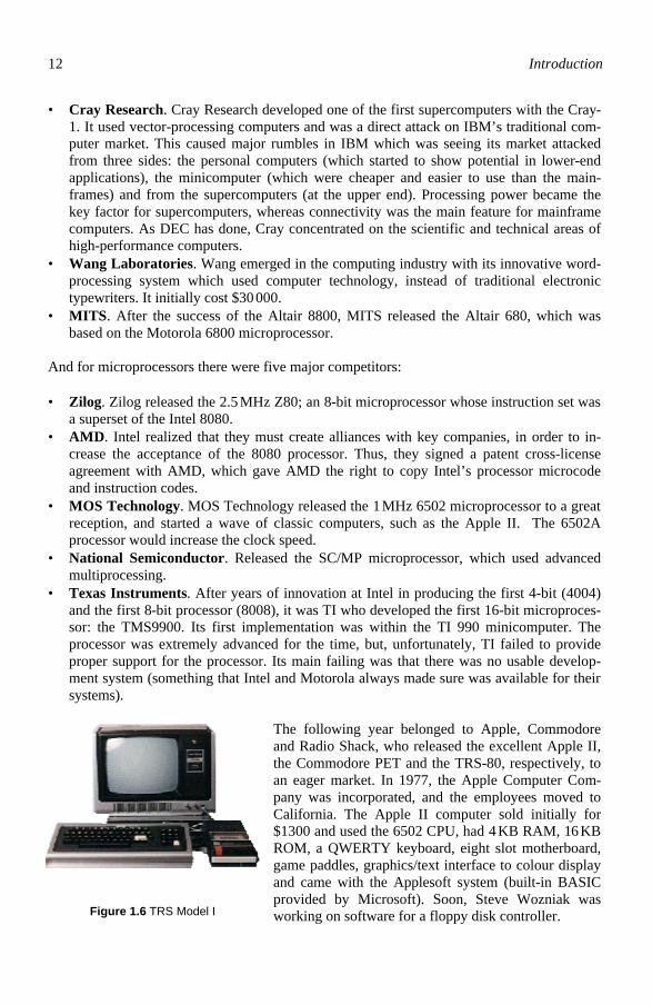
The following year belonged to Apple, Commodore and Radio Shack, who released the excellent Apple II, the Commodore PET and the TRS-80, respectively, to an eager market. In 1977, the Apple Computer Com-pany was incorporated, and the employees moved to California. The Apple II computer sold initially for $1300 and used the 6502 CPU, had 4 KB RAM, 16 KB ROM, a QWERTY keyboard, eight slot motherboard, game paddles, graphics/text interface to colour display and came with the Applesoft system (built-in BASIC provided by Microsoft). Soon, Steve Wozniak was working on software for a floppy disk controller. Figure 1.6 TRS Model I

Computer busses 13
In has been shown that a killer software application, or game, is required for the wide-spread adoption of a new computer system. This killer application occurred for the Apple II when Dan Bricklin developed the VisiCalc spreadsheet program. Unfortunately, for him, and fortunately for others, such as Lotus and Microsoft, he never patented his technology. If he had done this, he would have become a multibillionaire. Dan got the idea of the electronic spreadsheet while he sat in a class at Harvard Business School. He designed the interface, while his partner, Bob Frankston, wrote the code. The VisiCalc software ran on the Apple II computer, and had a significant effect on the sales of the computer. It has since been the fa-ther of all other spreadsheet programs, such as Lotus 123 and Microsoft Excel (Lotus even-tually bought the rights to VisiCalc for $800 000 in 1985), and was released in 1979. The Commodore PET 2001 was also based around the 6502 CPU, and had a simpler specification (4 KB RAM, 14 KB ROM, keyboard, display, and tape drive), but it only cost $600. In competition, and at the same price, Radio Shack developed the TRS-80 microcom-puter. It was based around the Z80 processor and had 4KB RAM, 4KB ROM, keyboard, black-and-white video display, and tape cassette, and sold well beyond expectations. Microsoft expanded their market by developing Microsoft FORTRAN for CP/M-based computers, and granted Apple Computer a license to Microsoft’s BASIC.
1.3 8086/8088
The third generation of microprocessors began, in June 1976, with the launch of the 16-bit processors, when Texas Instruments introduced the TMS9900. It initially used the TI 990 minicomputer. The processor never took-off as it lacked peripheral devices, and it was on May 1978 that Intel released the 8086 microprocessor. This processor was mainly an exten-sion to the original 8080 processor and thus retained a degree of software compatibility. Intel first introduced the 4.77 MHz 8086 microprocessor, which had 16-bit registers, a 16-bit data bus, and 29 000 transistors, using three-micron technology. It had a 20-bit address bus and could thus access 1MB of memory. It had good performance at 0.33 MIPS and initially sold for $360 (maybe a joke at the expense on the IBM System/360). Later speeds included 8 MHz (0.66 MIPS) and 10 MHz (0.75 MIPS). IBM’s designers, after discussions with Bill Gates, realized the power of the 8086 and used it in the original IBM PC and IBM XT (eXtended Technology). It had a 16-bit data bus and a 20-bit address bus, and thus has a maximum addressable capacity of 1 MB, and could handle either 8 or 16 bits of data at a time (although in a messy way). Its main competitors were the Motorola 68000 and the Zilog Z8000. It was important for Intel to keep compatibility with 8080. The difficulty was that the 8080 used a 16-bit address (64 KB or 65 ,536 locations), whereas the 8086 would use a 20-bit address bus, allowing up to 1 MB of memory to be addressed. Thus, the 8086 was designed with a segmented memory, where the memory was segmented in 64 KB chunks. The 20-bit address was then made up of a segment address, and an offset address. In February 1979, Intel released the 8086 processor as follows: The Intel 8086, a new microcomputer, extends the midrange 8080 family into the 16-bit arena. The chip has attributes of both 8- and 16-bit processors. By executing the full set of 8080A/8085 8-bit instructions plus a powerful new set of 16-bit instructions, it enables a system designer familiar with existing 8080 devices to boost performance by a factor of as much as 10 while using essentially the same 8080 software package and development tools.
14 Introduction
The goals of the 8086 architectural design were to extend existing 8080 features symmetri-cally, across the board, and to add processing capabilities not to be found in the 8080. The added features include 16-bit arithmetic, signed 8- and 16-bit arithmetic (including multiply and divide), efficient interruptible byte-string operations, and improved bit manipulation. Significantly, they also include mechanisms for such minicomputer-type operations as reen-trant code, position-independent code, and dynamically relocatable programs. In addition, the processor may directly address up to 1 megabyte of memory and has been designed to support multiple-processor configurations. The 8086 and 8088 were binary compatible with each other, but not pin compatible. Binary compatibility means that either microprocessor could execute the same program. Pin incom-patibility means that you cannot plug the 8086 into the 8088, and vice-versa, and expect the chips to work. The new ‘x86’ devices implemented a CISC (Complex Instruction Set Com-puter design methodology). At the time, many companies were promoting RISC as the fast-ing processor technology. Intel would eventually win the CISC battle with the release of the Pentium processor, many years in the future. At the time, Intel Corporation struggled to supply enough chips to feed the hungry as-sembly lines of the expanding PC industry. Therefore, to ensure sufficient supply to the per-sonal computer industry, they subcontracted the fabrication rights of these chips to AMD, Harris, Hitachi, IBM, Siemens, and possibly others. Amongst Intel and their cohorts, the 8086 line of processors ran at speeds ranging from 4 MHz to 16 MHz. The Z80 processor, which had beaten the 8080 processor in many ways, led the way for its new 16-bit processor: the Z8000. Zilog had intended that it was to be compatible with the previous processor. Unfortunately, the designer decided to redesign the processor, so that it had an improved architecture, but was not compatible with the Z80. From that time on, Zilog lost their market share, and this gives an excellent example of compatibility winning over superior technology. The 8086 design was difficult to work with and was constrained by compatibility, but it allowed easy migration for system designers. IBM realized the potential of the PC and microprocessor. Unlike many of their previous computer systems, they developed their version of the PC using standard components, such as Intel’s 16-bit 8086 microprocessor. They released it as a business computer, which could run word processors, spread sheets and databases and was named the IBM PC (Figure 1.7). It has since become the parent of all the PCs ever produced. To increase the production of this software for the PC they made information on the hardware freely available. This resulted in many software packages being developed and helped clone manufacturers to copy the origi-nal design. So the term ‘IBM compatible’ was born and it quickly became an industry stan-dard by sheer market dominance. On previous computers, IBM had written most of their programs for their systems. For the PC they had a strict time limit, so they first went to Digital Research who was responsi-ble for developing CP/M, which was proposed as a new standardised operating system for microprocessors. Unfortunately, for Digital Research, they were unable to reach a final deal because they could not sign a strict confidentiality agreement. They then went to a small computer company called Microsoft. For this Bill Gates bought a program called Q-DOS (often called the Quick and Dirty Operating System) from Seattle Computer Products. Q-DOS was similar to CP/M, but totally incompatible. Microsoft paid less than $100 000 for the rights to the software. It was released on the PC as PC-DOS, and Microsoft released their own version called MS-DOS, which has since become the best selling software in history, and IBM increased the market for Intel processors, a thousand times over.

Computer busses 15
To give users some choice in their operating sys-tem, the IBM PC was initially distributed with three operating systems: PC-DOS (provided by Microsoft), Digital Research’s CP/M-86 and UCSD Pascal P-System. Microsoft understood that to make their op-erating system the standard, that they must provide IBM with a good deal. Thus, Microsoft offered IBM the royalty-free rights to use Microsoft’s operating system forever, for $80 000. This made PC-DOS much cheaper than the other two (such as $450 for P-System, $175 for CP/M and $60 for PC-DOS). Mi-crosoft was smart in that they allowed IBM to use PC-DOS for free, but they held the control of the licensing of the software. This was one of the great-est pieces of business ever conducted. Eventually
CP/M and P-System died off, while PC-DOS become the standard operating system for the PC. The developed program was hardly earth shattering, but has since gone on to make bil-lions of dollars. It was named the Disk Operating System (DOS) because of its original pur-pose of controlling the disk drives. Compared with some of the work that was going on at Apple and at Xerox, it was a very basic system. It had no graphical user interface and accepted commands from the keyboard and displayed them to the monitor. These commands were interpreted by the system to perform file management tasks, program execution and system configuration. Its function was to run programs, copy and remove files, create direc-tories, move within a directory structure and to list files. To most people this was their first introduction to computing, but for many, DOS made using the computer too difficult, and it would not be until proper graphical user interfaces, such as Windows 95, that PCs would truly be accepted and used by the majority. It did not take long for the computer industry to start ‘cloning’ the IBM PC. Many com-panies tried; but most of them failed because their BIOS were not compatible with IBM PC BIOS. Columbia, Kayro and others went by the wayside because they were not totally PC compatible. Compaq eventually broke though the compatibility barrier with the introduction of the Compaq portable computer. Compaq’s success created the turning point that enabled today’s modern computer industry. They produced sales of $111 million in the first year of their operation, making it the fastest growing company in history. In Japan, NEC bought a license on the 8086/8088. They improved the design and pro-duced two Intel ‘clones’, called the V20 (8088-compatible) and V30 (8086-compatible). The V-series ran approximately 20% faster than the Intel chips when running at the same clock speed. Therefore, the V-series chips provided a cheap upgrade to owners of the IBM-PC and other clones computers. Although these chips were pin compatible with the 8086 and 8088, they also had some extensions to the architecture. They featured all of the ‘new’ instructions on the 80186/80188, and also were capable of running in Z80 mode (directly running pro-grams written for the Z80 microprocessor). Much to Intel’s embarrassment, NEC refused to pay royalties to NEC on the sale of their processors. Intel found that it was difficult to copy-right the actual silicon design, and have since copyrighted the microcode, which runs on the processor. The microcode for the 8086/8088 consisted of 90 different mini-programs. How-ever, in a courtroom, NEC showed that they had not copied these mini-programs and had designed their own. At this time, Intel was loosing a great deal of their memory product to Japanese compa-
Figure 1.7 IBM PC

16 Introduction
nies. Their focus, from now on, would be the PC-processor market. If they could always keep one step ahead of the cloners they would have a virtual monopoly. Eventually they would become so powerful as a market leader that they would overcome the basic rule that you always need a second source of processors for new processors to be accepted in the mar-ket. IBM had developed a system that would end up reducing their market share, and create a quasi-monopoly at the end of the 1990s and the beginning of the millennium for Intel (with processors and support devices) and Microsoft (for operating systems, and eventually appli-cation software). IBM would eventually fail in its introduction of new industry standards, such as MXA bus technology, whereas Intel would gain acceptance of new standards, such as the PCI bus, and Microsoft would develop new standard in operating systems, such as Windows NT. At the same time as Intel was developing the 8086 they were developing the 8800 proc-essor, which would not be compatible with the 8080, and would be a great technological break-though (as it would not have to be compatible with the older 8080 device). When the 8800 was finally released in 1981 as the iAPX432 (Intel Advanced Processor Architecture), it reached the market just as the IBM PC took off, and died a quick death, as everyone wanted the lower-powered 8086 device. The iAPX lives on as the ‘x86’ architecture. Apple was growing fast in 1978 and released a BASIC version of VisiCalc spreadsheet. They also produced their first Apple II disk drive and Disk II, which was a 5.25-inch floppy disk drive linked to the computer by a cable ($495). At the end of 1978, Apple Computer began work on an enhanced Apple II with custom chips, code-named Annie, a supercom-puter with a bit-sliced architecture, code-named Lisa, and also on Sara (the Apple III). Atari released the Atari 400 and 800 personal computers, which used the 6502 processor. Micro-soft was quick to spot the potential of the 8086 processor and developed Microsoft COBOL and Microsoft BASIC for it. Computer systems also started to find their way into social pursuits when Atari developed the Asteroids computer game and Taito developed the Space Invaders arcade game. They were classics of their time, but hardly powerful by today’s bit-mapped, 3D graphics. Epson, who had had a successful market in typewriters, started to produce low-price, high-performance dot matrix printers (the MX-80), and at the same time, Commodore re-leased the CBM 2020 dot-matrix printer (as well as a dual 5.25-inch floppy disk drive unit). In 1979, Xerox finally lost its foothold on the computer industry when the Alto was ad-vertised on TV, but then the president decides to drop its development. Microsoft, on the other hand, was going from strength to strength. Microsoft 8080 BASIC eventually broke the one million-dollar barrier, the first microprocessor product to do this. Soon, Microsoft had developed BASIC, and FORTRAN for the 8086. They had also released Assembler language system for 8080/Z80 microprocessors. Apple Computer released DOS 3.2, and the Apple II Plus computer, which had a 48 KB memory, and cost $1195. They also highlighted their growing strength by introduces their first printer, the Apple Silentype ($600). At PARC, Xerox was the leader in developing a graphical user interface with their Alto computer. As a learning process, a group of engineers and executives from Apple were given a demonstration of the Alton, and its associated soft-ware, in exchange for Xerox spending $1 million buying 100 000 Apple Computer shares. The investment would pay off many times over for Apple as it helped in their development of the Apple Mac computer. 1979 produced mixed fortunes for two of Intel’s competitors: Zilog and Motorola. It was a bad year for Zilog when it distributed its new 16-bit processor, the Z8000. It main draw-back was its incompatibility with its 8-bit predecessor, the classic Z80. For Motorola, it was one of success as they released the excellent 68000, 16-bit microprocessor. It used 68 000

Computer busses 17
transistors (thus, its derived name). Radio Shack continued development of their TRS-80 computer (Figure 1.8), with the TRS-80 Model II, and Texas Instruments introduced the TI-99/4 personal computer ($1500). Atari also started to distribute Atari 400 (8 KB memory, $550) and Atari 800 ($1000) personal computers. In the UK, Clive Sinclair created Sinclair Re-search, and was distended to develop classic com-puters, such as the ZX81 and the Sinclair Spectrum. He had already been a major innovator in the 1960s and the 1970s, with watches, audio amplifiers and pocket calculators. In the main these were extremely successful however, he was also destined to develop an electric car (Sinclair C5), which had the opposite effect on sales as he had had with his computer sys-tems. A key to the acceptance, and the sales of a com-puter was its software. This was in terms of its oper-ating systems and its applications. Initially it was games that were used with the PCs, but three impor-tant application packages were released, these were: • Spreadsheet. The VisiCalc software was released for the Apple II at a cost of $100. Ap-
ple Computer eventually tried to buy the company, which developed VisiCalc, for $1 million in Apple stock, but Apple’s president refuses to approve the deal. Its eventual rights would have been worth much more than this small figure.
• Wordprocessor. MicroPro released the WordStar word processor (written by Rob Ba-rnaby). It is available for Intel 8080A and Zilog Z80-based CP/M-80 systems. Apple Computer also released AppleWriter 1.0. The following year (1980) would see the re-lease of the popular WordPerfect (from Satellite Software International).
• Database. The Vulcan database program, which become known at dBase II. Two new companies were created in 1979, which would become important industry leaders in peripherals. These were Seagate Technologies (founded by Alan Shugart founded in Scotts Valley, California), and Hayes Microcomputer Products who produced the 110/300-
baud Micromodem II for the Apple II ($380). The following year (1979) saw Radio Shack (with their TRS-80 range), Commodore (with the PET range), Apple Computer (with their Apple II/III) and Microsoft at the forefront of the personal computer market. Two new companies joined the growing personal computer market, at different ends of technology. At the bottom end, which covered the games and hobby market, Sinclair Re-search appeared, and at the top end of the market, the workstation end, which was aimed at serious applications, came Apollo. Clive Sinclair in the UK had started Sinclair Research. He had already Figure 1.9 TRS-80 Model III
Figure 1.8 TRS-80 Color

18 Introduction
had a significant effect on the electronics industry. In the 1960s, he had developed hi-fi, am-plifier and radio kits for hobbyists, and then in the 1970s he had further developed into calcu-lators, multimeters and, even, pocket TVs. His main market in the 1980s would be personal computers, and it was on price that his company would gain the most on his competitors. The major developments of the year were: • Radio Shack. In 1980, Radio Shack followed up their success of the TRS-80, with the
TRS-80 Model III (Figure 1.9). It was based around the Zilog Z80 processor and was priced between $700 and $2500. They also released the TRS-80 Color Computer (Figure 1.8), which was based on the Motorola 6809E processor and had 4 KB RAM. It was priced well below the Model III and cost $400. Radio Shack at the time were innovating in other areas, and produced the TRS-80 Pocket Computer, which had a 24-character dis-play, and sold for $230.
• Apple Computer. Apple Computer accelerated their development work and released the Apple III computer. It was based on the 2 MHz 6502A microprocessor, and included a 5.25-inch floppy drive. It initially cost between $4500 and $8000. Work also began on the Diana project, which would eventually become the Apple IIe. The company was also floated on the stock market, where 4.6 million shares were sold at $22 a share. This made many Apple employees instant millionaires.
• Sinclair Research. Sinclair Research burst on the com-puter market place with the ZX80 computer. It was based on the 3.25 MHz NEC Technologies 780-1 proc-essor and came with 1 KB RAM and 4 KB ROM. It was priced at a cut-down rate of $200, but it was far from perfect. Its main drawback was its membrane type key-board.
• Intel. Along with development of the 8086 processor, Intel released a number of support devices, including the 8087math coprocessor.
• Microsoft. Microsoft released a Unix operating sys-tem, Microsoft XENIX OS, for the Intel 8086, Zilog Z8000, Motorola M68000, and Digital Equipment PDP-11.
• Hewlett-Packard. HP had developed a good market in powerful calculators, and pro-duced a mixture of a computer and a calculator, with the HP-85. It cost $3250, had a 32-character wide CRT display, a built-in printer, a cassette tape recorder, and a keyboard.
• Commodore. Commodore Business Machines enhanced their product range with the CBM 8032 computer, which had 32 KB RAM and an 80-column monochrome display. They also developed a dual 5.25-inch floppy disk drive unit (the CBM 8050). In Japan, Commodore released the VIC-1001, which would later become the VIC-20. It had 5 KB RAM, and a 22-column colour video output capability.
• Apollo. Apollo burst onto the computer market with high-end workstations based on the Motorola 68000 processor. They were aimed at the serious user, and their main applica-tion area was in computer-aided design. One of the first to be introduced was the DN300 (Figure 1.10), which was based around the excellent Motorola 68000 processor. It had a built-in mono monitor, an external 60 MB hard disk drive, an 8-inch floppy drive, built-in ATR (Apollo Token Ring) network card, and 1.5 MB RAM. It even had its own multi-user, networked operating system called Aegis. Unfortunately, for all its power and us-
Figure 1.10 Apollo DN300

Computer busses 19
ability, Aegis never really took off, and when the market demanded standardized operat-ing systems, Apollo switched to Domain/IX (which was a Unix clone). It is likely that Apollo would have captured an even larger market if they had had changed to Unix at an earlier time, as Sun (the other large workstation manufacturer) had done. The Token Ring network was excellent in its performance, but suffered from several problems, such as the difficulty in tracing faults, and the difficulty in adding and deleting nodes from the ring. Over time, Ethernet eventually became the standard networking technology, as it was relatively cheap and easy to maintain and install. Apollo attacked directly at the IBM/DEC mainframe/minicomputer market, and soon developed a large market share of the workstation market. The advantage that workstations had over mainframes is that each workstation had its own local resources, including a graphical display, and typically, windows/graphics-based packages. Mainframes and minicomputers tended to be based on a central server with a number of text terminals. Apollo were successful in developing the workstation market and their only real competitor was Sun. Hewlett-Packard eventually took Apollo over. However, Apollo computers, as with the classic computers, such as the Apple II and the Apple Macintosh, were well loved by their owners and some would say that they were many years ahead of their time. There are many occurrences of Apollo computers working continuously for five years, with only short breaks for Xmas holi-days, and so on. After a skilled network manager set them up, they tended to cause few problems. No crashes, no hardware problems, no network problems, no software incom-patibilities. Nothing. Aegis, as Unix does, supported a networked file system, where a global file system could be built up with local disk resources. Thus, a network of 10 workstations, each with 50 MB hard disks allowed for a global file system of 500 MB.
• Seagate Technology. Seagate become a market leader for hard disk drives when they developed a 5.25-inch Winchester disk, with four platters and a capacity of 5 MB.
• Philips/Sony. These companies developed the CD–Audio standard for optical disk stor-age of digital audio. At the same time, Sony Electronics introduced a 3.5-inch floppy disk and drive, double-sided, double-density, which had a capacity of 875 KB (but less, when formatted).
• Texas Instruments. TI were busy adding peripherals to their TI 99/4 computer, includ-ing a thermal printer (30 cps on a 5×7 character matrix), a command module ($45), a mo-dem, RS-232 interface ($225), a 5.25-inch mini-floppy disk drive which could store up to 90 KB on each disk. The floppy disk controller cost $300, and the disk drive cost $500.
• Digital Research. DR released CP/M-86 for Intel 8086- and 8088-based systems. Digital Research could have easily become the Microsoft of the future, but for a misunderstand-ing with IBM.
One of the few companies who developed a system around the Zilog Z8000 processor was Onyx. The Onyx C8002 microcomputer was a powerful computer which contained 256 KB RAM, a tape backup, a hard disk, serial ports for eight users, and the UNIX operating sys-tem. Its cost was $20000.
1.4 80186/80188
Intel continued the evolution of the 8086 and 8088 by, in 1982, introducing the 80186 and 80188. These processors featured new instructions, new fault tolerance protection, and were

20 Introduction
Intel’s first of many failed attempts at the x86 chip integration game. The new instructions and fault tolerance additions were logical evolutions of the 8086 and 8088. Intel added instructions that made programming much more convenient for low-level (assembly language) programmers. Intel also added some fault tolerance protection. The original 8086 and 8088 would hang when they encountered an invalid computer instruc-tion, whereas the 80186 and 80188 added the ability to trap this condition and attempt a re-covery method. Intel integrated this processor with many of the peripheral chips already employed in the IBM PC. The 80186/80188 integrated interrupt controllers, interval timers, DMA controllers, clock generators, and other core support logic. In many ways, the device was produced a decade ahead of its time. Unfortunately, this device did not catch on with many hardware manufacturers; this spelled the end of Intel’s first attempt at CPU integration. However, this device has enjoyed a tremendous success in the world of embedded processors. If you look on your high performance disk driver or disk controller, you might still see an 80186 being used. Eventually, many embedded processor vendors began manufacturing these devices as a second source to Intel, or in clones of their own. Between the various vendors, the 80186/80188 was available in speeds ranging from 6 MHz to 40 MHz.
1.5 80286
In 1982, Intel introduced the 80286. For the first time, Intel did not simultaneously introduce an 8-bit bus version of this processor (such as the 80288). The 80286 introduced some sig-nificant microprocessor extensions. Intel continued to extend the instruction set; more sig-nificantly, Intel added four more address lines and a new operating mode called ‘protected mode’. The 8086, 8088, 80186 and 80188 all contained 20 address lines, giving these proc-essors one megabyte of addressibility (220 = 1 MB). The 80286, with its 24 address lines, gives 16 megabytes of addressibility (224 = 16 MB). For the most part, the new instructions of the 80286 were introduced to support the new protected mode. Real mode was still limited to the one megabyte program addressing of the 8086, et al. Essentially, a program could not take advantage of the 16-megabyte address space without using protected mode. Unfortunately, protected mode could not run real-mode (DOS) programs. These limitations thwarted attempts to adopt the 80286 programming ex-tensions for mainstream consumer use. During the reign of the 80286, the first ‘chipsets’ were introduced. These were nothing more than a set of devices that replaced dozens of other peripheral devices, while maintain-ing identical functionality. Chips and Technologies became one of the first popular chipset companies. IBM was spurred by the huge success of the IBM PC and decided to use the 80286 in their next generation computer, the IBM PC-AT. However, the PC-AT was not introduced until 1985, which was three years after introduction of the 80286. IBM, it seems, were actu-ally frightened by the thought of the 32-bit processors as they allowed PCs to challenge their thriving minicomputer market. A new threat to the PC emerged from Apple, who used the Motorola 68000 processor, with an excellent operating system, to produce the Apple Mac computer. It had a full graphical user interface, which was based around windows and icon, and had a mouse pointer to allow users to easily move around the computer system.

Computer busses 21
Like the IBM PC, the PC-AT was hugely successful for home and business use. Intel continued to second-source the device to ensure an adequate supply of chips to the computer industry. Intel, AMD, IBM and Harris were now producing 80286 chips as OEM products, whereas Siemens, Fujitsu, and Kruger either cloned it, or were also second sources. Between these various manufacturers, the 80286 was offered in speeds ranging from 6 MHz to 25 MHz. Intel had had considerable trouble providing enough 8086/80186 processors, and had created technology-sharing agreements with companies such as AMD. This also allowed companies to have a second source for processors, as many organizations (especially mili-tary-based organizations) did not trust a single-source supply for a product. In 1984, it was estimated that Intel could only supply between one-fifth and one-third of the current demand for the 80186 device. For the coming 80386 design, Intel decided to break the industry prac-tice of second sourcing and go on their own.
1.6 Post-PC development
IBM dominated the computer industry in the 1950s and 1960s, and it was only in the 1970s that their quasimonopoly started to erode but, at the time, most of their competitors feared their power. If a competitor released a new product, they would often sit back and wait for IBM to trump them, with a better product that had the magical IBM badge. Few companies had the sales turnover to match IBM in research and development. This was shown to great effect with the development of the System/360 range, which had one of the largest ever re-search and development budgets ($5 billion). After initial development setbacks, the Sys-tem/360 range was a great success and paid off the initial investment, many times over. IBM sold over 50 000 System/360 computers in a period of six years, and then replaced it with the System/370 series, which was one of the first computers with memory made from integrated circuits. In 1981, IBM started the long slide from front-runner to also-ran, and within ten years, their own child (the IBM PC) would match the power of their own mainframes. For example, when the Pentium was released, in 1989, it had a processing power of 250 MIPS, while the IBM System/370 mainframe had, at the time, a processing power of 400 MIPS. IBM even, in the development of the IBM AT computer, tried to slug the power of the PC so that it would not impinge on their lucrative mainframe market. As will be seen, IBM, after the overwhelm-ing success of the IBM PC, made two major mistakes: • The PCjr. The PCjr quickly sank without trace, as it was not compatible with the IBM
PC. The time and money spent on the PCjr was completely wasted and gave other manu-facturers an opportunity to clone, and improve on the original IBM PC.
• Missing the portable market. IBM missed the IBM PC portable market, and when they did realize its potential, their attempt was inferior to the market leader (Compaq Com-puters). Later, though, they would produce an excellent portable, called the ThinkPad, but, by that time, they had lost a large market share to companies such as Toshiba, Com-paq and Dell.
After making these mistakes, other factors continued to affect their loss of market share. These included:

22 Introduction
• Initially missing the market for systems based on 32-bit microprocessors (80386). IBM missed the 32-bit processor when they developed their AT and PS/2 ranges of com-puters, as, initially, they used the 16-bit 80286. This had been intentional, as IBM did not want to make their new computer too powerful, as they would start to compete with their lucrative mainframe market.
• Trying to move the market towards MCA. After IBM realized that they had lost the bat-tle against the cloners, they developed their own architecture: MicroChannel Architec-ture (MCA), which would force manufacturers to license the technology from them. Un-fortunately, for IBM, Compaq took over the standard as they introduced a computer, which used standard IBM PC architecture, but improved on it as they used the new Intel 80386 in their DeskPro range. IBM would, in time, come back into the fold and follow the rest in their architecture. From then on, IBM became a follower rather than a leader.
After loosing a large market share, IBM soon realized, after the failure of MCA, that they had also lost the market leadership for hardware development. They then decided to try to turn the market for operating system software, with OS/2. It was becoming obvious that the operating system held the key to the hardware architectures, and application software. In a perfect world, an operating system can hide the hardware from the application software, so the hardware becomes less important. Thus, if the software runs fast enough, the hardware can be of any type and of any architecture, allowing application programmers to write their software for the operating system and not for the specific hardware. Whichever company developed the standards for the operating system would hold the key to hardware architec-ture, and also the range of other packages, such as office tools, networking applications, and so on. OS/2 would eventually fail, and it would be left to one company to lead in this area: Microsoft. Not even the mighty Intel could hold the standards, as Microsoft holds the key link between the software and the hardware. Their operating system would eventually de-couple the software from the hardware. With the Microsoft Windows NT operating system, they produced an operating system that could run on different architectures. Unfortunately, for IBM, OS/2 was a compromised operating system, which was devel-oped for all their computers, whether they be mainframes or low-level PCs. Unlike the de-velopment of the PC, many of the organizational units within IBM, including the powerful main-frame divisions, had a say about what went into OS/2 and what was left out. For the IBM PC, the PC team at Boca Raton was given almost independence from the rest of the organization, but the development of OS/2 was riddled with compromises, reviews and specification changes. At the time, mainframes differed from PCs in many different ways. One of the most noticeable ways was the way that they were booted, and the regularity of system crashes. Most users of PCs demanded fast boot times (less than a minute, if possible), but had no great problems when it crashes at a few times a day. These crashes were typically due to incorrectly functioning and configured hardware, and incorrectly installed software. In the mainframe market, an operating system performs a great deal of system checks and tries to properly configure the hardware. This causes long boot-up times, and is not a problem with a mainframe, which will typically run for many weeks, months, or years without requir-ing a re-boot. However, for the PC, a boot time of anything more than a few minutes is a big problem. In the end, OS/2 had too long a boot time, and was too slow (possibly due to its complexity) to compete in the marketplace. In total, IBM spent over $2 billion on OS/2 with very little in return. It is perhaps ironical that new versions of the Microsoft operating system perform a great deal of system checks and try to configure the system each time it is booted. Now, though, this can now be done in a relatively short time, as the hardware is a great deal
Computer busses 23
faster than it was when graphical user interfaces first reached the market. Another casualty of the rise of the IBM PC was DEC. As IBM had done with the Sys-tem/360 range, DEC invested billions of dollars in their VAX range, which became an unbe-lievable success. As Compaq Computers would do in the 1980s, DEC achieved unbelievable growth, going from its foundation in 1957 to a sales turnover of $8 billion in 1986 (the peak year for DEC, before the PC destroyed the market for minicomputers). The introduction of the PC would see the end of computer manufacturing for Osborne, Altair, Texas Instruments and Xerox. Going in the opposite direction were the new compa-nies such as Compaq Computers, Sun Microsystems, Apollo (for a while), Cray and Micro-soft. Compaq Computers, in 1981, generated $110 million in their first year, a further two years on it was $503.9 million, and two years after that it was $1 billion. The following year it was $2 billion. From zero to $2 billion, in six years (a world record, at the time). Microsoft was another high-growth company going from $16 million in 1981 to $1.8 billion in 1991. In most years, Microsoft doubled its size. Consistently Microsoft was also highly profitable with at least 30 % of sales resulting in profit, and at least 10% invested in research and de-velopment. The next 20 years would also see the creation of many computer-related multibil-lionaires, such as Bill Gates who, within in twenty years, would be worth almost $100 bil-lion. Before the introduction of the IBM PC, the biggest threats to IBM came, at the top end from DEC and at the bottom end from Apple. Both companies could do little wrong. DEC released their classic PDP-11, and then followed it up with the VAX range. Apple quickly developed their range of computers, and moved from a mainly game-playing computer, to one which could be used for game playing and also for business applications. For Apple, the key to the move into the business environment was the introduction of VisiCalc. From the 1980s, software would become the dominant driving force, and the best hardware in the world could not make up for a lack of application software. 1981 would become a pivotal year for the development of computers. Before this year, different computer standards thrived, and incompatibility reigned. After it, there would only be one main standard, which would be a truly open standard, which would be driven not by IBM, but by Intel and Microsoft. At the time, the computer industry split itself into two main areas: • Serious/commercial computers. Mainly IBM and DEC with their range of mainframe
computers and minicomputers. Within 10 years, both IBM and DEC would change to be different companies. IBM would end up loosing their quasi-monopoly on computers sys-tems, and DEC would end up being taken over by Compaq, who would evolve from the new market created by IBM.
• Hobby/home/game-playing computers. These computers had grown from the basic 8-bit processors, such as the 6502 and the Z80. The main product leaders were Commo-dore, Sinclair, Apple, Osborne, Altair, Acorn, Radio Shack and Xerox.
Few of these computers, at the time, were compatible with each other, and it was a great ad-vantage to a manufacturer that their computers were incompatible with others, as software written for one would not work on another. For example, the Apple II and the Commodore PET were based on the same processor, but had incompatible hardware, especially with the graphics system. It was in 1981 that IBM released, ahead of schedule, the IBM 5150 PC Personal Com-puter. It featured the 4.77 MHz Intel 8088 processor, 64 KB RAM, 40 KB ROM, one 5.25-

24 Introduction
inch floppy drive (160 KB capacity), and PC-DOS 1.0 (Microsoft’s MS-DOS). It cost $3000, and could be installed with Microsoft BASIC, VisiCalc, UCSD Pascal, CP/M-86, and Easy-writer 1.0. Another version used a CGA graphics card, which gave 640×200 resolution with 16 colours. At the time, many of the other computer companies were following up the success of their previous products, and few had any great worries of the business-oriented IBM PC. The main developments were: • Commodore. After its release in Japan, Commodore eventually released the VIC-20 to
an eager world market. It has a full-size 61-key keyboard, 5 KB RAM (expandable to 32 KB), 6502A CPU, a 22×23 line text display, and colour graphics. It initially sold for $299, and at its peak, it was being produced at 9 000 units per day.
• Sinclair. Sinclair followed up the success of the ZX80 with the ZX81, which was re-leased for $150 (in the USA it was released as the TS1000), and was based on the Z80A processor. Within 10 months, over 250 000 were sold.
• Apple. Apple was very much a market leader, and would eventually be the only real competitor to the IBM PC. In 1981, they reintroduced the Apple III, which was their first with a hard disk. In 1981, Apple Computer got into a little bit of trouble over the Apple name, as The Beatles used it for their record company (Apple Corps Limited). Eventu-ally, Apple Computer signed an agreement allowing them to use the Apple name for their business, but they were not allowed to market audio/video products with recording or playback capabilities.
• Osborne. The Osborne Computer Corporation was going from strength to strength, and if not for the release of the IBM PC would have been a major computer manufactures. In 1981, they released the Osborne 1 PC, which was based on the Z80A processor and in-cluded a 5-inch display, 64 KB RAM, keyboard, a keypad, modem, and two 5.25-inch 100 KB disk drives. It sold for $1795, but included CP/M, BASIC, WordStar, and Super-Calc. Sales were much great than expected, in fact they sold as many in a single month as they expected for their total sales (up to 10 000 per month).
• Xerox. Xerox continued to innovate and released the Star 8010, which contained many of the features that were used with the Alto, such as a bitmapped screen, WYSIWYG word processor, mouse, laser printer, Smalltalk language, Ethernet, and software for combining text and graphics in the same document. It sold for the unbelievably high price of $16 000. This price, especially up against the IBM PC, was too great for the market, and it quickly failed. At the same time, Xerox was planning the Xerox 820 (code named The Worm), which would be based on the 8-bit Z80 processor, whereas the new IBM PC was based on the 16-bit 8088. It, like the Star 8010, was doomed to fail. These were classic cases of releasing the products at the wrong time, for the wrong price.
• Acorn. In the UK, Acorn Computer released an excellent computer named the BBC Mi-crocomputer System. It was quickly adopted for a UK TV program, which the BBC was running to introduce microcomputers. Against the ZX81, it had an excellent specification, such as being based on the 6502A processor, addressing up to 48 KB RAM, and a 16-color graphics display. Its great advantage, though, was that it had a real keyboard (and not a horrible membrane keyboard, like the ZX81). The BBC TV program was a great success in the UK, and so was the BBC Microcomputer.
Two other companies that became industry leaders, developed products in 1981. These were Novell Data Systems and Aston-Tate. Novell created a simple networking operating system

Computer busses 25
that allowed two computers to share a single hard disk drive. Soon Novell would develop their Novell NetWare operating system, which allowed computers to share resources over a network. Ashton-Tate released the dBase II package which was the standard database pack-age for many years. For Intel, the adoption of the 8088 in the IBM PC was a godsend, and they had great dif-ficulties keeping up with the supply of the processor. Unlike the 8080, though, they did not actively seek AMD for a second source for the processor. Intel had learnt that some second -source rights caused problems when the second source company actually moved ahead of them in their technology. Typically, second- source companies are able to charge a lower rate, as they do not have to recoup the initial research and development investment. Intel would eventually seek other companies, and AMD sought out Zilog for second source rights for their up-and-coming Z8000 device. It seemed to AMD that Zilog would have greatest potential for their new device, as they had shown with their Z80 device. Intel was starting to realise that the processor market was a winner as it had a great deal of intellectual effort added to it. It differed from the memory market where designs could be easily copied by competitors. With microprocessors, they could set new standards and pro-tect their designs with copyrights. If they established a lead in the processor market, and kept one step ahead of the copiers, they could make a great deal of profit in releasing new prod-ucts and producing support devices for their processors, especially for the 8086/8088. For this, Intel released the 8087 math coprocessor, which greatly speeded up mathematical calcu-lations, especially floating point ones. The use of floating point long division would eventu-ally come back to haunt Intel, when a college tutor discovered a bug in their Pentium proces-sor. Intel were an innovative company, and had produced the first 4-bit and the first 8-bit processor, but with the 16-bit market they were beaten by Texas Instruments (TI). Unfortu-nately, for TI, the TMS 9900 was a rehash of an earlier product, and was generally under-powered. Intel, though, had the great strength in their 8088 processor of releasing a whole series of support devices which made it easier for designers to integrate the new processor. Anyway, no one could have guessed the impact that the IBM PC would have on the market. Intel was also beaten by National Semiconductor for the first 32-bit processor (the 32000). The year 1982 would see IBM throw open the market for computers, with the IBM PC, and also through two great mistakes. Apart from IBM, five other companies would dominate the year: Commodore, Sinclair, Compaq, Apple and Sun. Three of them, Commodore, Apple and Sinclair, were from the old school, and the other two, Compaq and Sun Microsystems, were from the new school, and would learn to adapt to the new ‘serious’ market in comput-ing that the IBM PC had created. In the same year, the US Justice Department threw out an antitrust lawsuit filed against IBM 13 years earlier. Within 15 years, it would be Microsoft who was facing similar action. At IBM, the PC was taking off in ways that could never have been imagined. The IBM PC was a work of genius in which everything had been planned with perfection. It would sell over 200 000 computers within 12 months of its introduction, but the following year would see two major mistakes by IBM. The first was the introduction of the PCjr, which was inten-tionally incompatible with the IBM PC (because IBM did not want it to effect the IBM PC market) and the IBM AT. The PCjr failed because of its incompatibility, whereas the AT failed as it used a 16-bit processor (the 80286), while other computers were released using the new Intel 32-bit processor (the 80386). IBM could have easily have overcome these drawbacks, but, as these developments involved a much wider team than the IBM PC, they were held back by the interests of other parties. For example, the mainframe division was keen for the AT to use 16-bit processors, rather than the more powerful 32-bit processors, as

26 Introduction
this could further erode their market. These two decisions would open the door to the new kid on the block – Compaq. Three former Texas Instruments managers founded Compaq Computer Corporation in 1982: Rod Canion, Jim Harris, and Bill Murto. Their first product was Compaq Portable PC. It was released in the following year (1983), and cost $3000. The Compaq Portable was to-tally compatible with the IBM PC and used the Intel 8088 (4.77 MHz), had 128 KB RAM, a 9-inch monochrome monitor and had a 320 KB 5.25-inch disk drive (Sony Electronics in the same year demonstrated the 3.5-inch microfloppy disk system). A large part of the start-up finance was used to create a version of the ROM BIOS which was IBM compatible, but did not violate IBM’s copyright – a stroke of genius that many failed to follow. Compaq would soon become the fastest growing company ever. Only in the computer industry could a com-pany grow from zero to hundreds of millions of dollars within 12 months. Compaq created a new market, which was based on IBM PC compatibility. They then waited for the great IBM to come along and sink their product, but when IBM did produce a portable, it was too late, too heavy, and failed to match the Compaq in its specification. Compaq were not in fact the first company to clone the IBM PC as they finally released it in 1983 – that was achieved by Columbia Data Products, with their MPC. Two companies who would battle against the PC for market share were Sun and Apple. Sun Microsystems would quickly become a major computer company, and derived its name from an acronym from the Stanford University Network. Their first product was the Sun 1 workstation computer. They, like Apple, fought the IBM in terms of architecture and operat-ing system. Sun, almost single-handedly, made the Unix operating system popular. Their computers succeed in the market, not because they were compatible with any other com-puter, but because they were technically superior to anything that the IBM PC could offer. The software that ran on the system fully used the processing power of the processor, and the Unix operating system provided an excellent robust and reliable operating system. Compati-bility can often lead to a great deal of problems, especially if the compatibility involves the 8088 processor. At Apple, champagne corks were popping, as they became the first PC company to gen-erate $1 billion in annual sales. The Apple II Plus and Apple II had sold over 750 000 units. After toying with the Lisa computer and new versions of the Apple II, Apple would have one more trump card up their sleeve: the Apple Macintosh. Microsoft was keen to work with Apple, in case the relationship with IBM did not work out, and signed an agreement to de-velop applications for the forthcoming Macintosh (of which Microsoft were given an initial prototype to work on). IBM had become slightly annoyed with the success of Microsoft, from the success of their own creation. For Microsoft, it was a no-lose situation. They were, in the main, sharing code across the two architectures, which would quickly become industry standards. One would become an open standard (the IBM PC), and the other would be a closed standard (the Apple Mac). The year 1982 saw a fantastic growth at Intel, and the only way that they could keep up with demand was to license their products to other silicon design companies. For this, they signed a 10-year technology exchange agreement with Advanced Micro Devices (AMD) that focused on the x86 microprocessor architecture. This agreement would be later regretted as AMD started to overtake them in the 80486 market. Intel, in the same year, released an up-date to the 8086 processor, called the 80286. The processor was destined for the IBM AT computer and it ran initially at 6 MHz, which improved on the 4.77 MHz of the 8088 proces-sor. It had a 16-bit data bus, like the 8086, but had an extended 24-bit address bus that gave it an addressing range of 16 MB, rather than the 1 MB addressing range of the 8086/8088, or 1 GB of virtual memory. It outperformed the 8086 with a throughput of 0.9 MIPS, but this

Computer busses 27
increased to 1.5 MIPS with a 10 MHz clock and 2.66 MIPS with a 12 MHz clock. Commodore was never slow at developing their products. After the success of the Vic-20, in 1981, they released the Commodore 64 in the following year. It sold for $600 and had an excellent specification based around the new 6510 processor, and was released with 64 KB RAM, 20 KB ROM, sound chip (the first PC to have integrated sound), eight sprites, 16-colour graphics, and a 40-column screen. It was the first personal computer with an inte-grated sound synthesizer chip. They then released a whole range of peripherals, such as the VIC Modem ($110). Commodore also moved into the business market, with the BX256 and B128 computers for $3000 and $1700, respectively. The BX256 was a 16-bit multiprocessor computer. It included 256 KB RAM, Intel 8088 for CP/M-86, 6509 CPU, 80-column B/W monitor, built-in dual disk drives, and three-voice sound. The B128 computer featured 128 KB RAM, 40 KB ROM, 6509 CPU, 5.25-inch floppy drive, three-voice sound chip, car-tridge slot, and an 80-column green screen. At Sinclair, the ZX81 had been an unbelievable success and, knowing that alone they could not succeed in the USA market, they signed an agreement with the Timex Corporation to license Sinclair computers in the USA. By the end of 1982, Sinclair Research had sold over 500 000 ZX81s in over 30 countries. Atari also become a major computer company with the Atari 800. Its main feature was an advanced graphics display. Radio Shack also released the powerful TRS-80 Model 16. It used a 16-bit Motorola MC68000 microprocessor, a Z80 microprocessor, had 8-inch floppy drives, and an optional 8 MB hard drive. At the same time as Compaq were releasing their portable, Radio Shack produced the TRS-80 Pocket Com-puter; unfortunately, it was relatively slow as it used a 1.3 MHz 8-bit microprocessor, with a 26-character display. DEC also finally decided to enter the personal computer market with the dual-processor Rainbow 100. It had an excellent specification with both a Z80 and an 8088 microprocessor, and could run CP/M, CP/M-86 or MS-DOS. Unfortunately, at $3000, it was too expensive for the market, which was already hot for the IBM PC. 1983 was a mixed year for IBM. They continued their success with the released of the IBM PC XT. It sold for $5000 and had a 10 MB hard drive, three extra expansion slots, and a serial interface. In its basic form it had 128 KB RAM, and a 360 KB floppy drive. With the success of PC-DOS 1.0, IBM followed it up with PC-DOS 2.1. On the downside, IBM re-leased the IBM PCjr, which cost $700. The greatest winners in 1983 were the newly created Compaq Computers, and Microsoft. In their first year, Compaq sold 47 000 computers, with a turnover of $111 million (and raised $67 million on their first public stock offering). They would eventually reach the $1 billion within five years of their creation. The other winner was Microsoft who knew that they had to completely rewrite the MS-DOS operating system, so that it coped better with current and future systems. For this they introduced MS-DOS 2.0, which supported 10 MB hard drives, a tree-structured file system, and 360 KB floppy disks. They had quickly released the potential of the IBM PC, and re-leased XENIX 3.0 (a PC version of Unix), Multi-Tool Word for DOS (which would eventu-ally become Microsoft Word 1.0), as well as producing the Microsoft mouse (which sold for $200, with interface card and mouse). Microsoft also announced, in 1983, that it would be developing Microsoft Windows (initially known as Interface Manager), which would even-tually be released in 1985. At the same time as Microsoft announced Windows, IBM was developing a program called TopView, and Digital Research was developing GEM (Graph-ics Environment Manager). These programs would use DOS as the basic operating system, but would allow the user to run multiple programs. The great problem with TopView was that it was text based and not a graphical user interface (GUI, or ‘gooey’). Even allowing for

28 Introduction
this, most predicted, because of IBM’s strength, that TopView would become the standard user interface. If IBM had won the battle for the user interface, they would have probably taken over the standard for both the user interface and the operating system, and then eventu-ally the standard for the architecture. IBM, though, did agree to work with Microsoft on OS/2. Microsoft would eventually invest hundreds of millions of dollars on OS/2, with little in return. Businesses must learn from their mistakes, and Microsoft has always done this. The expertise gained in developing OS/2 was used in the development of Microsoft Win-dows. In the same year as Microsoft released their new version of MS-DOS, AT&T was releas-ing the version of Unix that would become a standard: Unix System V. It was the first at-tempt at bringing together the different versions of Unix, including XENIX, SunOS and Unix 4.3 BSD. The two main families of Unix have become Unix System V and BSD (Berkeley Software Distribution) Version 4.4. System V would eventually be sold to SCO (Santa Cruz Operation). Currently available Unix systems include AIX (on IBM workstations and main-frames), HP-UX (on HP workstations), Linux (on PC-based systems), OSF/1 (on DEC work-stations) and Solaris (on Sun workstations). Other attempts at standardising Unix occurred with X/Open, OSF, and COSE, but have mainly failed. The great strength of Unix is its communications and networking protocols (such as TCP/IP, SMTP, SNMP, and so on), which provide the foundation for the Internet. Many organizations have tried to create a new operating system, such as VMS (from DEC) and Aegis (Apollo), but only Unix has become a serious competitor to Microsoft in operating systems. In the PC market, they would totally dominate the market, although Linux (a Unix clone) created a small market share for the technical experts. Unix-based systems used the standardised networking software that was built-into Unix, but the PC still lacked any proper form of networking. So, in 1983, Novell create one of the standards of the PC networking market: the Novell NetWare network operating system. The only other operating system which could have competed again Microsoft’s DOS and Windows, was the up-and-coming Mac OS from Apple, which was at least 10 years ahead of its competitors. However, Apple refused to license their system to other vendors, or to other computer manufacturers. Another significant event in software development occurred at AT&T, when Bjarn Stroustrup designed the new object-oriented language C++. Its great strength, and also one of its weaknesses, was that it was based on the popular C programming language. Its usage is now widespread and most current applications have been written using C++, whether they be for microcomputers, minicomputers and mainframe computers. The main drawback of C++ was that programmers could still use the C programming language, which, because of its looseness and simplicity, allowed the programmer to produce programs that would compile, but could crash because of a run-time error which was due to badly designed software. Typi-cal errors were running off the end of an array, bad parameter passing into modules, or using memory that was not reserved for other purposes. Object-oriented programming languages are much tighter in their syntax, and the things that are allowed to be done. Thus, the com-piler will typically catch more errors, whether they are run-time or syntax errors, before the program is run. Java has since overcome the problems of C++, as it is totally object-oriented, and much tighter in the rules of software coding. The great strength for the adoption of the PC was IBM’s intention to allow software com-panies to quickly develop application software. They thus released information on the hardware of the computer so that software companies could write compatible applications. Like VisiCalc for the Apple II, in 1983, the two killer applications to help boost the accep-tance, and sales, of the IBM PC were:

Computer busses 29
• Lotus 1-2-3. This was a spreadsheet designed and developed by Jonathan Sachs and Mitch Kapor at Lotus Development. It initially required an extremely large amount of memory, 256 KB. Over $1 million was spent on its initial promotion but, it paid back its original investment a thousand times over. Its sales hit Microsoft’s Multiplan spread-sheet, which had sold over 1 million copies. Microsoft learnt from this, and in the coming years would release Excel, which would become the standard spreadsheet.
• WordPerfect. This was a word processing package developed by Satellite Software In-ternational (who would eventually change their name to the WordPerfect Corporation.). It initially cost $500, and was an instant success. Many believed that WordPerfect 5.1 was the classic touch-type program, as it used keystrokes instead of long-winded menu op-tions. Many typists have since had real troubles moving from WordPerfect to WIMPs-based packages such as Microsoft Word (so much so that many current word processors support all of the WordPerfect keystrokes).
The year 1983 was to be bleak for non-IBM PC compatible computers and saw prices falling month upon month. It also spelt the end of the line, in different ways, for three great innova-tors in the personal computer industry: Zilog, Osborne and Texas Instruments. It was the beginning of the end for Zilog when they released their 32-bit microprocessor: the Z8000. It was an advanced device that had a 256-byte on-chip cache, instruction pipelining, memory management, and 10–25 MHz clock speed. Unfortunately, for Zilog, it was incompatible with the great Z80 processor. It thus failed in the market against the strength of the Intel 8086, and the up-and-coming 80386 processor. Of the many computer manufacturers who rushed to the market and used the 8086/8088, only one, Commodore, introduced a Z8000-based system (Commodore Z8000). Apart from the failings at IBM and DEC, the release of the Z8000 processor must rank amongst the poorest decisions in computing history. No one could predict the effect that a Z80-compatiable 32-bit processor would have had on the mar-ket. Certainly a 32-bit processor, which was functionally compatible with the 8086/8088 (as the Z80 had been with the 8080) would have blown the market wide open, and would have possibly stopped the slide to quasimonopoly of the Intel processors. Another failure in the processor market was the extremely powerful 6 MHz, 32-bit NS32032 microprocessor from National Semiconductor. Commodore Business Machines were becoming dominant in the home computers mar-ket, and highlighted their dominance with the release of the Commodore 64, for $400, which quickly fell to $200 and dropped the prices of the VIC-20 to below $100 (breaking it for the first time). In 1983, the sales of the VIC-20 reached 1 000000. Commodore was also keen to develop the business market, and released the Commodore Executive 64. It cost $1000 and had 64 KB RAM, a detachable keyboard, a 5-inch colour monitor, and a 170 KB floppy drive. In 1983, Commodore became the first personal com-puter to sell over $1 billion worth of computers. Many companies in the home computer market had made large profits, but one failure in a product range could spell disaster for a company. The high profits for all would not last long as Commodore, Atari and Sinclair started slashing prices. Sinclair, through Timex, in-troduced the Timex/Sinclair 2000 in the USA (which was called the Sinclair Spectrum in other countries). It cost $149 for a 16 KB model, while the ZX81 price was reduced to $49. The squeeze was on, as prices tumbled. Atari released their 600XL for $199, and ceased production of the Atari 5200. The 600XL was based on the 1.79 MHz 6502C processor, had 16 KB RAM, 24 KB ROM, and an optional CP/M module. As the push was on from other manufacturers to reduce prices, they

30 Introduction
also did the same and reduced the Atari 800 to $400. Atari also released the 1200XL home computer, which had 64 KB RAM, and 256 colour capability, and cost $900. Production eventually ended for the 1200XL, mainly because of compatibility problems. At the time, Japanese companies had been making great advances in the electronics in-dustry, and many, such as NEC and Fujitsu were starting to overtake USA silicon companies, such as Texas Instruments, Intel and National Semiconductor, in their product of integrated circuits (although Intel had the x86 series of processors as their trump card). They were also winning in producing peripherals and accessories for computer systems, such as: • Fujitsu producing the first 256 Kbit memory chips. • Sony developed a new standard for 3.5-inch floppy disks, with the Microfloppy Industry
Committee, and thus created the first double-sided, double-density, holding floppy disk system that could store up to 1 MB. Sony was also working with Philips in creating the CD-ROM, which was an extension of audio CD technology.
However, in computer manufacturing, Japanese companies struggled as the USA companies, such as IBM and Apple, were setting the standards. The IBM PC was relatively easy to clone, but the Apple computer required a license to manufacture, which, at the time, was almost impossible to gain. Compared with many USA-based companies, the Japanese com-panies were efficient and produced reliable electronics, but as long as they were one step behind the US-based computer companies, they could not gain a serious share of the home computer market. To overcome this, 14 Japanese companies and Microsoft joined an alliance to create the MSX standard It used the Zilog Z80, TI TMS9918A video processor, General Instruments AY-8910 sound processor, NEC cassette interface chip, Atari joystick interface, 64 KB RAM, and 32 KB ROM-based extended Microsoft BASIC. This was one of the first attempts to standardize computer architecture, but was doomed to failure with the release of the IBM PC, and that it was based on 8-bit technology. Several MSX computers did reach the market, but quickly failed. It was a great idea, and one that should have worked. The key to its failure was that there was a better, more defined standard: the IBM PC. In a classic case of releasing the right product at the wrong time, Osborne Computer re-leased their own portable computer. Unlike the IBM PC, or Compaq’s portable, it was based on the Z80A processor. The computer quickly failed in the market and Osborne eventually filed for bankruptcy. Around the same time, Radio Shack also produced a non-IBM compati-ble portable: the TRS-80 Model 100. They were also following the tried and tested technique of improving their product line by releasing the TRS-80 Model 4. It would fail as it cost $2000, and was non-IBM PC compatible (as it was based on the 4 MHz Zilog Z80A micro-processor). Against the IBM PC, and the lower-end computers, such as the VIC-64 and the Sinclair Spectrum, it was vastly overpriced. Another casualty of the success of the IBM PC was Texas Instruments who eventually withdrew from the personal computer market. The TI 99/1 had sold well over the years (over 1 million), but was now struggling against the new, cheaper computers. Apple took a big gamble with the LISA1 (local integrated software architecture) com-puter, as it cost $50 million, and its software cost $100 million (showing that the costs of developing hardware were reducing, while software development costs were increasing). It was released in 1984 and was expensive ($10 000), it was underpowered, but it was the first personal computer to have a graphical user interface (GUI). Rather than going with the 8086,
1 LISA was actually named after Steve Job’s young daughter.

Computer busses 31
as most of the market was doing, they based it on the excellent 5 MHz 68000 microprocessor. It had 1 MB RAM, 2 MB ROM, a 12-inch black/white monitor, 720×364 graphics, dual 5.25-inch 860 KB floppy drives, and a 5 MB hard disk drive. LISA would sell over 100 000 units. Apple was keen to develop the LISA computer, but it would be the new Mac, which would become the focus for their operation. Apple was investing a great deal of effort in the Mac, and gave the Mac developers the best environment possible. This caused considerable friction with the Apple II division, as all the finances for the Mac facilities were generated from sales of the Apple II. Apple inten-tionally kept the two divisions apart, which only helped to increase the friction. In the year, the Apple II highlighted its success by selling its 1 millionth unit. They continued its devel-opment with the Apple IIe, which had 64 KB RAM, Applesoft BASIC, upper/lower case keyboard, seven expansion slots, 40×24 and 80×24 text, 1 MHz 6502 processor, up to 560×192 graphics, and a 140 KB 5.25-inch floppy drive. The software market, especially related to the IBM PC was growing fast. Satellite Soft-ware International released WordPerfect 3.0 for $500, and Borland International, founded by Philippe Kahn, created the first version of their excellent Turbo Pascal compiler. Borland, single-handily, saved Pascal from an early exit. Borland were for years the main company involved in producing software development tools for the PC, with Borland C++, Borland Delphi and Borland JBuilder. Unfortunately, they would eventually struggle against the might of Microsoft (who were able to invest a great deal of money into their development tools, especially in Visual Basic and Visual C++). Microsoft has the privileged position of being able to invest money in other areas of development, but redirecting them from profits made from other areas. For example, they used profits from the DOS system to invest in Windows, and profits from Windows to invest into office applications (Word, Excel and PowerPoint), and profits from office applications to invest into software development tools (Visual Basic, Visual C++ and Visual Java). Obviously, it is to Microsoft’s advantage that they keep the tools up-to-date, as this is the same development system that they use to gener-ate their own applications.
1984 obviously had futuristic connotations to it. However, it was less of a futuristic year for IBM and more of a nightmare, when IBM released the IBM PCjr. It used the 8088 CPU, includes 64 KB RAM, a ‘Freeboard’ keyboard (IBM would eventually release a new key-board, which was a free upgrade to those who wanted it), and one 5.25-inch disk drive, and no monitor, for $1300. A year later, in 1985, the PCjr was dropped. As the market became more competitive, IBM started to show their teeth as the number of cloners increased. The unfortunate companies who were the first to be taken to court were Corona Data Systems and Eagle Computer. IBM sued them over a copyright violation of the IBM PC’s BIOS, and eas-ily won the case. It was clear that, to avoid litigation, that companies required rewriting the BIOS. This would not give a technical advantage, but would keep IBM’s lawyers away.
The next step for IBM was important in the development of the PC. For this they learned from their mistakes with the PCjr, and made their new computer, the PC AT, compatible with the IBM PC. It used the new Intel 6MHz 80286 processor, and had a 5.25-inch 1.2 MB floppy drive, with 256 KB or 512 KB RAM, optional 20 MB hard drive, monochrome or col-our monitor. The initial cost was $4000.
As the demand for IBM PCs increased, there was also an increase for demand for graph-ics adaptors. For this IBM released the Enhanced Color Display (EGA) monitor with 640×350 resolution, 16 colours, at a cost of $850. They also released TopView which failed in the market because it was text-based, and not a GUI. If they had done, they may have cap-tured the market which Microsoft Windows gained.

32 Introduction
The battle for the processor market started to heat up when Intel released the 80188, which was an integrated version of the 8086. They also allowed IBM the legal rights to use microlithography masks to make x86 processor chips. Intel, having survived the new 32-bit processors, from Zilog and National Semiconductor, faced their biggest threat from NEC and Motorola. NEC was the first to clone the 8088, with the 8 MHz V20 microprocessor and a clone of the 8086 processor, with the 8 MHz V30 microprocessor. Another threat came from Motorola who added the 68010 and 68020 32-bit processors to their range. Many non-PC-based developers adopted the Motorola processor in favour of the 8086, as it was typically easier to develop hardware for it, and much easier to write software (as the 8086 had a horri-ble segmented memory architecture). For most, it was the only way for a computer manufac-turer to differentiate themselves from the clone market. Some, such as Radio Shack, fol-lowed the IBM PC market with the Tandy 1000/1200 HD, but there was little to differentiate their clone from any other clone. New entries for the year included Silicon Graphics, who would go on to produce excel-lent workstations, which had state-of-the-art graphics power. In 1984, they produced the first 3D graphics workstation. They were also involved, in the 1990s, in the development of the graphics for Jurassic Park. It was to be the year of Compaq Computer and Apple Computers. Compaq introduced the Compaq Deskpro. Apple Computer created the ultimate entry for their Macintosh computer, by running their 1984 advert once, during the NFL SuperBowl. The advert had cost $1.5 million, but soon became one of the most talked about adverts, ever. The Macintosh was as brilliant a computer as anyone could have conceived. It was designed by creative people, and not just by technocrats. It was a fully integrated unit, which could be easily ported from place to place. The Mac used the 8 MHz 32-bit Motorola 68000 processor, along with a 9-inch B/W screen, 512×342 graphics, 400 KB 3.5-inch floppy disk drive, mouse, and 128 KB RAM. It cost $2500. Microsoft knew that they could not just rely on the IBM PC market, so they worked closely with Apple and released Microsoft BASIC (MacBASIC) and Microsoft Multiplan for the Macintosh. After just 74 days of its introduction, over 50000 Macs had been sold, and after 100 days they had sold 70 0 00 units. After six months, it was 100 000 units, and within the year, 250 000 units. This, to Apple, was a great disappointment as they estimated that they would sell over 2 million units by the end of 1985. The main problem is that it lacked resources, especially memory. Apple Computer overcame this by releasing the Macintosh 512K for $3200. The Macintosh had everything going for it. It was a totally integrated system, where the IBM PC felt like a basic system, which required lots of extra bits and pieces to make it work properly. A great confusion at the time was the number of application packages which were entering the market. Apple eased this problem with the release of AppleWorks, which inte-grated a word processor, database management program, and a spreadsheet. Apple also continued developing the Lisa computer with Lisa 2, and also with the Apple II, with the Apple IIc computer (the Apple III computer had not sold well, and production of it soon stopped). The Apple IIc computer cost $1300 and was based on the 6502A processor, had 128 KB RAM and a 3.5-inch floppy disk drive. On the first day of its release, Apple re-ceived 52 000 orders. By the end of the year, over 2 million Apple II computers had been sold. The Lisa 2 computer came with 512 KB RAM, and a 10 MB hard disk. Apple was also innovating in the printer market, with the colour Apple Scribe printer and the LaserWriter. At the same time, Hewlett-Packard introduced the LaserJet laser printer, for $3600, with 300 dpi resolution. As Apple had done, Commodore would release, in the following year, a computer based

Computer busses 33
on the 68000 processor (the Amiga, from newly purchased Amiga Corporation). In 1984, they introduced the Commodore Plus/4 which used the 7501 microprocessor, had 64 KB RAM, 320×200 pixel graphics with 128 colours, and also released the Commodore 16 with 16 KB of RAM, at a selling price of $100. At Microsoft, development was continuing on both Apple and IBM PC systems. No one at the time could predict that the IBM PC market would eventually dwarf the Apple market. The Macintosh looked to be the system of the future, thus Microsoft stopped working on Excel, their new PC-based spreadsheet package, and switched their resources to developing software for the Macintosh. This included Excel for the Macintosh. From now on Microsoft would concentrate of GUI applications, for Microsoft Windows and for the Macintosh. They released MS-DOS 3.0/3.1 which supported larger hard disks, networks and high capacity floppy disks. After IBM lost out on the DOS operating system, Microsoft held out an olive branch to them by demonstrating Microsoft Windows. IBM refused to become involved, mainly because it competed with its newly developed interface, TopView. Microsoft and Lotus Development also nearly agreed to merge their companies, but Jim Manzi at Lotus Development convinced Mitch Kapor to back out of it. Microsoft’s Windows was superior to TopView as it used a graphical user interface. The only other real competitor to Microsoft was Digital Research, who had missed out on the IBM PC market. In 1984, they released the Graphics Environment Manager (GEM) icon/desktop user interface for the IBM PC com-puter. In the Unix market, in 1984, the Massachusetts Institute of Technology (MIT) began de-veloping the X Window System. Their main objective was to create a good windows system for Unix machines. Many versions evolved from this and, by 1985, it was decided that X would be available to anyone who wanted it for a nominal cost. X, itself, is a portable user interface and can be used to run programs remotely over a network. It has since become a de facto standard because of its manufacturer independence, its portability, its versatility and its ability to operate transparently across most network technologies and operating systems. The main features of X-Windows are that:
• It is network transparent. The output from a program can either be sent to the local graph-ics screen or to a remote node on the network. Application programs can output simulta-neously to displays on the network. The communication mechanism used is machine-independent and operating system independent.
• Many different styles of user interface can be supported. The management of the user interface, such as the placing, sizing and stacking of windows is not embedded in the sys-tem, but is controlled by an application program which can easily be changed.
• As X is not embedded into an operating system, it can be easily transported to a wide range of computer systems.
• Calls are made from application programs to the X-windows libraries which control WIMPs. The application program thus does not have to create any of these functions.
1985 was the year that Microsoft released their first version of Windows, at a price of $100. It was hardly startling, and would take another two versions before it completely dominated the market. It could not multitask, and still used DOS. Another major failing was that it did not use the full capabilities of the new 32-bit processor (80386) or the enhanced 16-bit proc-essor (80286), and could thus only access up to 1 MB of memory. Just as IBM were releasing their AT computer with the 80286, Intel released their new 32-bit 16 MHz 80386DX microprocessor, and the 80287 math coprocessor. The 80386 used
34 Introduction
32-bit registers and a 32-bit data bus, and incorporated 275 000 transistors (1.5 microns). The initial price was $299. It could access up to 4 GB of physical memory, or up to 64 TB of vir-tual memory. A worrying development for Intel came from the new start up company, Chips & Technologies, which developed a set of five chips that were equivalent to 63 smaller chips that were found on the IBM PC AT motherboard. This development meant that many of the support devices produced by Intel could be replaced by many less devices, thus cutting pro-duction costs. At Motorola, the success of the 68000 brought the 68008 processor. After Apple had released their 68000-based Macintosh in the previous year, Commodore released their new flagship computer: the Amiga 1000. Unlike the IBM PC, it was fully mul-titasking and used a WIMPs (windows, icons, menus and pointers) system. In its basic form it cost $1300 and had 256 KB RAM, and 880 KB 3.5-inch disk drive. They also released the Commodore 128 computer, which was an upgrade of the Commodore 64. Along with the Amiga, Commodore were trying to get into the PC market with the PC10 and PC20 com-puters, and tried to stop production of the Commodore 64 (but public demand restarted pro-duction several times). At Apple Computer the success of the Macintosh continued. The battle was now on for the PC market, and they had the IBM PC in their sights. During the SuperBowl, Apple ran a TV advert for Macintosh Office, which showed blindfolded business executives walking off a cliff, like lemmings. Things were becoming turbulent in Apple, after years of growth had produced a grown-up company with formal business methods. This type of environment did not suit Steve Jobs (the co-founder of Apple Computer), and he left, along with five senior managers, to form NeXT Incorporated. In fact, John Sculley, the former Pepsi-Cola president who, in 1984, had been brought in to train Steve to become the CEO, forced Steve Jobs out. From then on, John Sculley was the man in charge of Apple. The future for Apple looked difficult, but the key to future growth would be the Macin-tosh, and not Lisa or the Apple II. The software for the Macintosh was being produced as quickly as the market was buying it. Microsoft released Microsoft Word 1.0 and the Micro-soft Excel spreadsheet ($95). Apple were not really impressed with the first version of Excel, and reckoned that Lotus Development’s equivalent was better (named Jazz). Another key package for the Macintosh was Aldus PageMaker from Aldus, which created a new industry, which for the first time, integrated text and graphics with a design package: desktop publish-ing. For years, PageMaker was the de facto standard package for graphics design and desk-top publishing. Microsoft obviously had a foot in both the IBM PC and the Macintosh mar-ket, as they released Microsoft Word 2.0 for DOS, and QuickBASIC 1.0. The year produced many good deals for Microsoft, including: • Microsoft signed a deal with IBM for a joint-development agreement to work together
on future operating systems and environments. • Microsoft signed a deal with Apple to cover Apple’s copyrights on the visual display of
the Macintosh. • Microsoft purchased all rights to DOS from Seattle Computer Products for $925000.
The deal of the century! Atari struggled on, in face of the competition from Apple, Compaq, Commodore and the IBM PC. With the might of Microsoft added to the equation, they had little chance in the profitable business market. They continued their previous success in the home market with the 65XE, the 130XE, and the 520ST, for $120, $400, and $600, respectively. Radio Shack also continued to swim against the tide with the release of the Tandy 6000 multi-user system

Computer busses 35
(with up to nine users). It was extremely powerful and used the both a Z80A and a 68000 processor. It had 512 KB RAM, 80×24 text, graphics, 1.2 MB 8-inch disk, an optional 15 MB hard drive, TRS-DOS, or XENIX 3.0. Another struggler with an excellent product was Acorn who released The Advanced RISC Machine (ARM), which used a powerful 32-bit processor. At IBM, there was despondency as they stopped production of their PCjr and released their first version of TopView for $150. One of the successes of the previous year, Compaq Computer, was jubilant as they reported second year revenues of $329 million. They quickly followed up the success of the Compaq portable with the Compaq Deskpro 286 and Portable 286, which was similar in specification to the IBM AT. IBM also moved into networking with IBM Token Ring; unfortunately, even though Token Ring was an excellent networking technology, the future would be Ethernet. Each year in the computer industry had seen a new significant company being born. The previous years had seen the birth of Compaq Computers, Sun Microsystems and Apollo. In the 1985, it was Nintendo, and Chip and Technologies. Nintendo would become one of the leading computer companies in the lucrative computer games market. They again highlighted the strength of the USA in generating new and innovative computer companies. Software companies were also being created, such the Corel Corporation (by Michael Cowpland), and Quarterdeck Office Systems. On of the successes of the previous years was Sun Microsys-tems who had started work on their SPARC processor. On the PC, new software versions were coming thick and fast. Lotus 1-2-3 has moved to 2.0, WordPerfect moved to Version 4.1, Novell NetWare was now at Version 2.0 and dBase was at Version 3. 1985 also saw the first CD-ROM drives for computer use.
After a few frantic years, things started to settle down in 1986. The IBM PC and the Ap-ple Macintosh would now dominate the market, especially at the business end. One of the biggest winners was Compaq Computers who had seen their turnover for their third year rise to $503.9 million and, by the middle of the year, they would sell their 50 000th computer. Compaq Computer introduced the Compaq Portable II. Against its excellent quality and specification, IBM would eventually withdraw from the portable computer for a while, as it was obviously inferior to the Compaq portable. It would take many years before IBM would regain some of the portable market (with the ThinkPad). Compaq blasted the PC market wide open with the first 16 MHz Intel 80386-based PC: the Compaq Deskpro 386. The best that IBM could manage was the IBM AT which had an 8 MHz Intel 80286. The Deskpro 386 was thus running at twice the clock speed, and had the potential, with 32-bit software, to run twice as fast again. The 80386 also had significant improvements in the number of clock cycles that it took for an operation to be performed. Thus, the Deskpro 386 sprinted, while all the other PCs dawdled, and its full potential was yet to be realised. IBM knew that the PC was a compromised system, and released the IBM RT Personal Computer. This was based on a 32-bit RISC-based processor, with 1 MB RAM, a 1.2 MB floppy, and 40 MB hard drive, and cost $11 700. Even with the RISC processor, it only had a performance of 2 MIPS, and thus its price/performance ratio was too great for it to be adopted in the market. Apple was starting to suffer against the growing power of the IBM PC developers. They still had a closed system, where it was up to them to develop the software and hardware for the Macintosh, whereas the IBM had hundreds, if not thousands, working on it, and improv-ing it. The Apple Mac was now looking underpowered and lacking other facilities, especially in networking on IBM PC-based networks. Apple overcame part of this with the release of

36 Introduction
the Macintosh Plus, which was based around the 8 MHz 68000 processor, had 1 MB RAM, SCSI-based hard disk connector (the first ever computer to have integrated SCSI interfaces) and an 800 KB 3.5-inch floppy drive. It cost $2600 (while a 512 KB version cost $2000). Unfortunately, it was still not possible to connect an Apple Mac onto an IBM PC-based net-work, unless a telephone connection was used. This held it back from wider adoption in the commercial market. Apple, though, was starting to make great inroads into the publishing industry with the release of the innovative LaserWriter Plus printer. Microsoft had over the past few years initiated many new products for both the IBM PC, and the Apple Macintosh. In 1985, they consolidated their market with new versions of the successful software, such as MS-DOS 3.2 and Microsoft Word 3.0. In MS-DOS 3.2, support was added for 3.5-inch 720 KB floppy disk drives (these disks were much more reliable than the older, ‘floppy’, 5-inch floppy disk, as they had a hard case to protect them). The initial investment of time, and energy, for those involved in Microsoft was rewarded when, for the first time, Microsoft sold its shares to the public. When floated, each share was worth $21, which raised $61 million for Microsoft, and made Bill Gates the world’s youngest billion-aire. The UK also showed that they could innovate in market niches with the release of the Inmos T800 Transputer, which was a powerful RISC processor that could be used in parallel processing applications. Several computer manufacturers, such as Silicon Graphics, started to move towards the new range of RISC processors produced by MIP Technologies, such as the 8 MHz, 32-bit, R2000 processor. This used 110 000 transistors and gave a speed of 5 MIPS. At Motorola, they were working on the 68030 processor, which would have over 300 000 transistors. They also began work on the 88000 processor. At IBM, work had begun on a computer range which would become a classic: the IBM RS/6000 series. The newcomer of the year was Gateway 2000, which shipped its first PC. In addition, after using the Small Computer System Interface (SCSI) on Apple’s Macintosh (SCSI-1), it was standardised with the ANSI X3.131-1986 standard.
1.7 Exercises
The following questions are multiple choice. Please select from a–d. 1.7.1 Who solved the US Governments Census problems: (a) Bill Gates (b) Herman Hollerith (c) William Shockley (d) Lee De Forest 1.7.2 Which computer helped aid the British Government to crack codes in World War
II: (a) ENIAC (b) Harvard Mk I (c) IBM System/360 (d) Colossus 1.7.3 What is ENIAC an acronym for: (a) Electronic Numerical Integrator and Computer

Computer busses 37
(b) Electronic Number Interface Analysis Computer (c) Electronic Number Interface and Computer (d) Electronic Numerical Interchange Computer 1.7.4 Who invented the transistor: (a) Bill Gates (b) Herman Hollerith (c) William Shockley (d) Lee De Forest 1.7.5 Which company did William Shockley form: (a) Shockley Semiconductor (b) Shockley Devices (c) Shockley Electronics (d) Shockley Electrics 1.7.6 Which company proposed that silicon could be used for transistors: (a) IBM (b) Texas Instruments (c) Motorola (d) Fairchild Semiconductors 1.7.7 Which company first proposed the integrated circuit: (a) IBM (b) Texas Instruments (c) Motorola (d) Fairchild Semiconductors 1.7.8 Who first produced an integrated circuit: (a) John Cocke (b) Robert Noyce (c) Gordon Moore (d) William Shockley 1.7.9 Who proposed that the number of transistors that can be fitted onto an integrated
circuit doubles each year: (a) John Cocke (b) Robert Noyce (c) Gordon Moore (d) William Shockley 1.7.10 Which computer was the first to use integrated circuits: (a) Apple I (b) IBM System/360 (c) IBM PC (d) DEC PDP-11 1.7.11 Which one of the following formed Intel: (a) Bill Gates and Paul Allen (b) Robert Noyce, Gordon Moore and Andy Grove (c) Jerry Sanders (d) Steve Wozniak and Steve Jobs 1.7.12 Which one of the following formed Microsoft:

38 Introduction
(a) Bill Gates and Paul Allen (b) Robert Noyce, Gordon Moore and Andy Grove (c) Jerry Sanders (d) Steve Wozniak and Steve Jobs 1.7.13 Which one of the following formed Apple Computers: (a) Bill Gates and Paul Allen (b) Robert Noyce, Gordon Moore and Andy Grove (c) Jerry Sanders (d) Steve Wozniak and Steve Jobs 1.7.14 Which company did Kenneth Olsen help form: (a) Compaq (b) DEC (c) Microsoft (d) IBM 1.7.15 Which company developed the first microprocessor: (a) Texas Instruments (b) Motorola (c) Zilog (d) Intel 1.7.16 Which company developed the first 8-bit microprocessor: (a) NEC (780-1) (b) Motorola (6800) (c) Zilog (Z80) (d) Intel (8008) 1.7.17 Which company developed the first 16-bit microprocessor: (a) Texas Instruments (9900) (b) Motorola (68000) (c) Zilog (Z8000) (d) Intel (8086) 1.7.18 Which company was the first to demonstrate the usage of windows, mouse and
keyboard: (a) IBM (b) Xerox (c) Microsoft (d) DEC 1.7.19 Which company was the first to demonstrate the WYSIWYG concept: (a) IBM (b) Xerox (c) Microsoft (d) DEC 1.7.20 What was the name of the Xerox research center: (a) PARC (b) XRES (c) PERC (d) RESP 1.7.21 Which company did Bill Gates and Paul Allen initially create:

Computer busses 39
(a) Micro-Traffic (b) Traf-O-Data (c) Traffic Software (d) Gates & Allen 1.7.22 Who developed the C programming language: (a) Bill Gates and Paul Allen (b) Brian Kernighan and Dennis Ritchie (c) Niklaus Wirth (d) Steve Wozniak and Steve Jobs 1.7.23 Who developed the Pascal programming language: (a) Bill Gates and Paul Allen (b) Brian Kernighan and Dennis Ritchie (c) Niklaus Wirth (d) Steve Wozniak and Steve Jobs 1.7.24 Which was the first ever commercial microprocessor: (a) 4000 (b) 4004 (c) 8080 (d) 1000 1.7.25 The 8008 device could address up to 1 KB. Thus how much address lines did it
have: (a) 6 (b) 10 (c) 20 (d) 1000 1.7.26 Which processor did Zilog produce: (a) Z80 (b) 6502 (c) 8080 (d) 6800 1.7.27 Which processor did MOS Technology produce: (a) Z80 (b) 6502 (c) 8080 (d) 6800 1.7.28 Which processor did Motorola produce: (a) Z80 (b) 6502 (c) 8080 (d) 6800 1.7.29 Which processor did the Apple II use: (a) Zilog Z80 (b) MOS Technology 6502 (c) Intel 8080 (d) NEC 780-1

40 Introduction
1.7.30 Which processor did the Commodore PET use: (a) Zilog Z80 (b) MOS Technology 6502 (c) Intel 8080 (d) NEC 780-1 1.7.31 Which processor did the TRS-80 use: (a) Zilog Z80 (b) MOS Technology 6502 (c) Intel 8080 (d) NEC 780-1 1.7.32 Which processor did the ZX80 use: (a) Zilog Z80 (b) MOS Technology 6502 (c) Intel 8080 (d) NEC 780-1 1.7.33 Which company distributed CP/M: (a) Microsoft (b) Digital Research (c) Xerox (d) Applesoft 1.7.34 Which software language was standard on most early PCs: (a) C (b) BASIC (c) Pascal (d) Assembly Language 1.7.35 How did the Motorola 68000 gain its name: (a) No reason (b) It was sold for $680.00 (c) It sounded like the 8008 (d) It had 68 000 transistors 1.7.36 Which company produced the VAX range of computers: (a) IBM (b) DEC (c) Compaq (d) Apple
1.8 Notes from the author
The history of the PC is an unbelievable story, full of successes and failures. Many people who used some of the computer systems before the IBM PC was developed, wipe a tear from their eyes, for various reasons, when they remember their first introduction to computers, typically with the Sinclair Spectrum or the Apple II. In those days, all your programs could be saved to a single floppy disk, 128 KB of memory was more than enough to run any pro-gram, and the nearest you got to a GUI was at the adhesives shelf at your local DIY store. It must be said that computers were more interesting in those days. Open one up, and it was filled with processor chips, memory chips, sound chips, and so on. You could almost see the thing working (a bit like it was in the days of valves). These days, computers lack any soul;

Computer busses 41
one computer is much like the next. There’s the processor, there’s the memory, that’s a bridge chip, and, oh, there’s the busses, that’s it. As we move to computers on a chip, they will, in terms of hardware, become even more boring to look at. But, maybe I’m just biased. Oh, and before the IBM PC, it was people who made things happen in the computer industry, such as William Shockley, Steve Jobs, Kenneth Olson, Sir Clive Sinclair, Bill Gates, and so on. These days it is large teams of software and hardware engineers who move the industry. Well, enough of this negative stuff. The PC is an extremely exciting development, which has changed the form of modern life. Without its flexibility, its compatibility, and, especially, its introduction into the home, we would not have seen the fast growth of the Internet. Here are my Top 15 successes in the computer industry: 1. IBM PC (for most), which was a triumph of design and creativity. One of the few com-
puter systems to ever to be released on time, within budget, and within specification. Bill Gates must take some credit in getting IBM to adopt the 8088 processor, rather than 8080. After its success, every man and his dog had a say in what went into it. The rise of the bland IBM PC was a great success of an open system over closed systems. Compa-nies who have quasimonopolies are keen on keeping their systems closed, while compa-nies against other competitors prefer open systems. The market, and thus, the user, pre-fers open systems.
2. TCP/IP, which is the standard protocol used by computers communicating over the Internet. It has been designed to be computer independent to any type of computer, can talk to any other type. It has withstood the growth of the Internet with great success. Its only problem is that we are now running out of IP addresses to grant to all the com-puters that connect to the Internet. It is thus a victim of its own success.
3. Electronic mail, which has taken the paperless office one step nearer. Many mourned the death of the letter writing. Before email, TV and the telephone had suppressed the art of letter writing, but with email it is back again, stronger than ever. It is not without its faults, though. Many people have sent emails in anger, or ignorance, and then regret-ted them later. It is just too quick, and does not allow for a cooling off period. My motto is: ‘If you are annoyed about something sleep on it, and send the email in the morning’. Also, because email is not a face-to-face communication, or a voice-to-voice communi-cation, it is easy to take something out of context. So another motto is: ‘Carefully read everything that you have written, and make sure there is nothing’. Only on the Internet could email address format be accepted, worldwide, in such a short time.
4. Microsoft, who made sure that they could not lose in the growth of the PC, by teaming up with the main computer manufacturers, such as IBM (for DOS and OS/2), Apple (for Macintosh application software) and for their own operating system: Windows. Luckily for them it was their own operating system which became the industry standard. With the might of having the industry-standard operating system, they captured a large mar-ket for industry-standard application programs, such as Word and Excel.
5. Intel, who was presented with an enormous market with the development of the IBM PC, but have since invested money in enhancing their processors, but still keeping compati-bility with their earlier ones. This has caused a great deal of hassle for software devel-opers, but is a dream for users. With processors, the larger the market you have, the more money you can invest in new ones, which leads to a larger market, and so on. Un-fortunately, the problem with this is that other processor companies can simply copy their designs, and change them a little so that they are still compatible. This is some-thing that Intel have fought against, and, in most cases have succeed in regaining their

42 Introduction
market share, either with improved technology or through legal action. The Pentium processor was a great success, as it was technologically superior to many other proces-sors in the market, even the enhanced RISC devices. It has since become faster and faster.
6. 6502 and Z80 processors, the classic 16-bit processors which became a standard part in most of the PCs available before the IBM PC. The 6502 competed against the Motorola 6800, while the Z80 competed directly with the Intel 8080.
7. Apple II, which brought computing into the classroom, the laboratory and even the home.
8. Ethernet, which has become the standard networking technology. It is not the best net-working technology, but has survived because of its upgradeabliity, its ease-of-use, and its cheapness. Ethernet does not cope well with high capacity network traffic. This is be-cause it is based on contention, where nodes must contend with each other to get access to a network segment. If two nodes try to get access at the same time, a collision results, and no data is transmitted. Thus, the more traffic there is on the network, the more colli-sions there are. This reduces the overall network capacity. However, Ethernet had two more trump cards up its sleeve. When faced with network capacity problems, it in-creased its bit rate from the standard 10 Mbps (10 BASE) to 100 Mbps (100 BASE). So there was 10 times the capacity, which reduced contention problems. For networks backbones it also suffered because it could not transmit data fast enough. So, it played its next card: 1000 BASE. This increased the data rate to 1Gbps (1000 Mbps). Against this type of player, no other networking technology had a chance.
9. WWW, which is often confused with the Internet, and is becoming the largest, database ever created (okay, 99% of it is rubbish, but even if 1% is good then its all worthwhile). The WWW is one of the uses of the Internet (others include file transfer, remote login, electronic mail, and so on).
10. Apple Macintosh, which was one of few PC systems which competed with the IBM PC. It succeeded mainly because of its excellent operating system (MAC OS), which was ap-proximately 10 years ahead of its time. Possibly if Apple had spent as much time in de-veloping application software rather than for their operating system it would have con-siderably helped the adoption of the Mac. Apple refusing to license it to other manufac-turers also held its adoption back. For a long time it thus stayed a closed system.
11. Compaq DeskPro 386. Against all the odds, Compaq stole the IBM PC standard from the creators, who had tried to lead the rest of the industry up a dark alley, with MCA.
12. Sun SPARC, which succeed against of the growth of the IBM PC, because of its excel-lent technology, its reliable Unix operating system, and its graphical user interface (X-Windows). Sun did not make the mistakes that Apple made, and allowed other compa-nies to license their technology. They also supported open systems in terms of both the hardware and software.
13. Commodore, who bravely fought on against the IBM PC. They released mainly great computers, such as the Vic range and the Amiga. Commodore was responsible for forc-ing the price of computers down.
14. Sinclair, who, more than any other company, made computing acceptable to the masses. Okay, most of them had terrible membrane keyboards, and memory adaptor that wob-bled, and it took three fingers to get the required command (Shift-2nd Function-Alt etc). and it required a cassette recorder to download programs, and it would typically crash after you had entered one thousand lines of code. But, all of this aside, in the Sinclair Spectrum they found the right computer, for the right time, at the right price. Sometimes success can breed complacency, and so it turned out with the Sinclair QL and the Sin-

Computer busses 43
clair C-5 (the electric slipper). 15. Compaq, for startling growth, that is unlikely to be ever repeated. From zero to one bil-
lion dollars in five years. They achieved this growth, not by luck, but by shear superior technology, and with the idea of sharing their developments.
Other contenders include Hewlett-Packard (for their range of printers), CISCO (for their networking products), Java (for ignoring the make of the computer, and its network, and, well, everything), the Power PC (for trying to head off the PC, at the pass), Dell notebooks (because I’ve got one), the Intel 80386, the Intel Pentium, Microsoft Visual Basic (for bring-ing programming to the masses), Microsoft Windows 95, Microsoft Windows NT, and so on. Okay, Windows 95, Windows NT, the 80386 and the Pentium would normally be in the Top 10, but, as Microsoft and Intel are already there, I’ve left them out. Here’s to the Wintel Corporation. We are in their hands. One false move and they will bring their world around themselves. Up to now, Wintel have made all the correct decisions. When it comes to failures, there are no failures really, and it is easy to be wise after the event. Who really knows what would have happened if the industry had taken another route. So instead of the Top 15 failures, I’ve listed the following as the Top 15 under-achievers (please forgive me for adding a few of my own, such as DOS and the Intel 8088): 1. DOS, which became the best selling, standard operating systems for IBM PC systems.
Unfortunately, it held the computer industry back for at least 10 years. It was text-based, command-oriented, had no graphical user interface, could only access up to 640 KB, it could only use 16 bits at a time, and so on, … . Many with a short memory will say that the PC is easy to use, and intuitive, but they are maybe forgetting how it used to be. With Windows 95 (and to a lesser extent with Windows 3.x), Microsoft made computers much easier to use. From then on, users could actually switch their computer on without have to register for a high degree in Computer Engineering. DOS would have been fine, as it was compatible with all its previous parents, but the problem was MAC OS, which really showed everyone how a user interface should operate. Against this competition, it was no contest. So, what was it? Application software. The PC had application software coming out of its ears.
2. Intel 8088, which became the standard processor, and thus the standard machine code for PC applications. So why is it in the failures list? Well, like DOS, its because it was so difficult to use, and was a compromised system. While Amiga and Apple program-mers were writing proper programs which used the processor to its maximum extent, PC programs were still using their processor in ‘sleepy-mode’ (8088-compatiable mode), and could only access a maximum of 1 MB of memory (because of the 20-bit address bus limit for 8088 code). The big problem with the 8088 was that it kept compatibility with its father: the 8080. For this Intel decided to use a segmented memory access, which is fine for small programs, but a nightmare for large programs (basically anything over 64 KB).
3. Alpha processor, which was DEC’s attack on the processor market. It had blistering performance, which blew every other processor out of the water (and still does). It has never been properly exploited, as there is a lack of development tools for it. The Intel Pentium proved that it was a great all-comer and did many things well, and was willing to improve the bits that it was not so good at.
4. Z8000 processor, which was a classic case of being technically superior, but was not compatible with its father, the mighty Z80, and its kissing cousin, the 8080. Few compa-

44 Introduction
nies have given away such an advantage with a single product. Where are Zilog now? Head buried in the sand, probably.
5. DEC, who was one of the most innovative companies in the computer industry. They developed a completely new market niche with their minicomputers, but they refused to see, until it was too late, that the microcomputer would have an impact on the computer market. DEC went from a company that made a profit of $1.31 billion in 1988, to a company which, in one quarter of 1992, lost $2 billion. Their founder, Ken Olsen, even-tually left the company in 1992, and his successor brought sweeping changes. Eventu-ally, though, in 1998 it was one of the new PC companies, Compaq, who would buy DEC. For Compaq, DEC seemed a good match, as DEC had never really created much of a market for PCs, and had concentrated on high-end products, such as Alpha-based workstations and network servers.
6. Fairchild Semiconductor. Few companies have ever generated so many ideas and incu-bated so many innovative companies, and got so little in return.
7. Xerox. Many of the ideas in modern computing, such as GUIs and networking, were initiated at Xerox’s research facility. Unfortunately, Xerox lacked force to develop them into products, maybe because they reduced Xerox’s main market, which was, and still is, very much based on paper.
8. PCjr, which was another case of incompatibility. IBM lost a whole year in releasing the PCjr, and lost a lot of credibility with their suppliers (many of whom were left with un-sold systems) and their competitors (who were given a whole year to catch up with IBM).
9. OS/2, IBM’s attempt to regain the operating system market from Microsoft. It was a compromised operating system, and their development team lacked the freedom of the original IBM PC development. Too many people and too many committees were in-volved in its development. It thus lacked the freedom, and independence that the Boca Raton development team had. IBM’s mainframe divisions were, at the time, a powerful force in IBM, and could easily stall, or veto a product if it had an effect on their profit-able market.
10. CP/M, which many believed would become the standard operating system for micro-computers. Digital Research had an excellent opportunity to make it the standard oper-ating system for the PC, but Microsoft overcame them by making their DOS system much cheaper.
11. MCA, which was the architecture that IBM tried to move the market with. It failed be-cause Compaq, and several others, went against it, and kept developing the existing ar-chitecture.
12. RISC processors, which were seen as the answer to increased computing power. As Intel has shown, one of the best ways to increase computing speed is to simply ramp up the clock speed, and make the busses faster.
13. Sinclair Research, who after the success of the ZX81 and the Spectrum, threw it all away by releasing a whole range of under-achievers, such as the QL, and the C5.
14. MSX, which was meant to be the technology that would standardize computer software on PCs. Unfortunately, it hadn’t heard of the new 16-bit processors, and most of all, the IBM PC.
15. Lotus Development, who totally misjudged the market, by not initially developing their Lotus 1-2-3 spreadsheet for Microsoft Windows. They instead developed it for OS/2, and eventually lost the market leadership to Microsoft Excel. Lotus also missed an excellent opportunity to purchase a large part of Microsoft when they were still a small company. The profits on that purchase would have been gigantic.

Computer busses 45
So was/is the IBM PC a success? Of course it was/is. But, for IBM it has been a double-edged sword. It opened up a new and exciting market, and made the company operate in ways that would have never been possible before. Before the IBM PC, their systems sold by themselves, because they were made by IBM. It also considerably reduced their market share. Many questions remained unanswered: ‘Would it have been accepted in the same way if it had been a closed system, which had to be licensed from IBM?’ ‘Would it have been ac-cepted if it had used IBM components rather than other standard components, especially the Intel processors?’, ‘Would they have succeeded in the operating system market if they had written DOS by themselves?’, and so on. Who knows? But, from now on we will refer to those computers based on the x86 architecture as PCs. Oh, and as an academic I would like to give a special mention to the C programming language, which has given me great heartaches over the years. Oh, yeah, it’s used exten-sively in industry and is extremely useful. It is the programming language that I would auto-matically use for consultancy work. C is well supported by the major language package de-velopers, and there is a great deal of code available for it. But for teaching programming, it is a complete non-starter. Without going into too much detail, the problems with C are not to do with the basic syntax of the language. It’s to do with a thing called pointers. They are the most horrible things imaginable when it comes to teaching programming languages, and they basically ‘point’ to a location in memory. This is fine, but in most cases you don’t really have to bother about where in memory things are stored. But, C forces you to use them, rather than hiding them away. So, in a C programming class, things go very well until about the 8th week, when pointers are introduced, and then that’s it. Oh, and don’t get me started on C++.
1.9 DEC
The main rival to IBM before the advent of the PC was DEC (Digital Equipment Corpora-tion). They were formed in 1957, and grew to become the second largest computer company in the world. Their unbelievable growth, and fall, is a lesson for any industry. Brothers Ken-neth Olson and Stanley Olson, and Harlan Anderson started DEC on a start-up capital of $70 000 (which was 70% owned by American Research and Development Corporation). This should compare this with the start-up capital of Compaq, which was $10 million). DEC had an initial clear strategy, which was to make cheap computers, which appealed to the special-ist scientific and technical market. At the time, IBM had a quasimonopoly, and DEC did not have a chance to compete with them on a like-for-like product range. DEC eventually thrived because they attacked a small market niche with technically superior products. At the time, they could not possibly compete with IBM in the larger commercial market, where IBM had made a considerable investment. So, DEC turned to the scientific and technical market, which required relatively small and configurable products. DEC could not compete with the mighty IBM, who had a solid foundation of great marketing and sales teams. DEC was basi-cally a company of engineers, and they were proud of it. Their main product was the mini-computer, which was much cheaper than mainframes, but had a great deal of power, and could be easily configured and managed by a small group. The big winner for DEC was the PDP (Programmed Data Processor) series, which be-come the foundation of many scientific and engineering groups. No research group or indus-
46 Introduction
trial company was complete without a PDP computer. By today’s standards, there was more power in a pocket calculator, as there was in the PDP-8. It was also relatively large, weighing 250 pounds, and came in a rack-mounted unit which was over 6 feet tall. However, the PDP range was much cheaper than IBM mainframes. For example, the PDP-1 sold for $120 000, while the comparable IBM computer cost millions. The PDP range also introduced comput-ing to many young minds. Two exceptional minds, Bill Gates and Paul Allen, cut their teeth on a DEC PDP-8, where they wrote programs to support the BASIC programming language. The next great winner for DEC was the VAX (Virtual Address eXtension) computer which cost billions to develop, but was a great technical and commercial success. It covered the complete range of computer hardware from basic terminal interface up to large main-frame computers. For the first time, DEC produced every part of the computer system: the operating system, the hardware and the software. One of the great successes of the VAX range was the VMS operating system (produced by David Culter). It allowed computer pro-grammers to create programs which had more memory than the computer actually had (a virtual memory), and allowed several programs to run at the same time (multitasking). After the success of VMS, David Culter eventually went on develop a RISC operating system, but DEC management cancelled the project. After this he left DEC in disgust and went to Micro-soft to lead the development of the Windows NT operating system. Microsoft and Intel have strong recruitment policies, and often hire the best brains in the computer industry. In these days of networked computers, it is difficult to believe, but, at the time, the VAX range was a radical concept. Before VAX computers, DEC, with their PDP range, was never touched $7.6 billion. Unfortunately, DEC’s bubble burst for two reasons. The first was the really a threat to IBM’s core market in mainframes. However, the VAX range was. The fu-ture looked destined to be DEC’s, and not IBM’s. In 1986, their sales reached $2 billion, and soon recession of the 1990s. It was a situation that many companies had difficulty coping with, but it could not be avoided. The only reason was one that could have been avoided if DEC had realized the changing market, and the power of the new 16-bit microprocessors. It was basically the IBM PC which eventually beat IBM’s mainframes and DEC’s minicom-puters on performance, at a fraction of the price, from whichever company you wanted. DEC actually, in 1979, had the opportunity to enter into the PC market when they allowed Heath-Kit to sell the PDP-11 minicomputer in kit form. At the time, DEC believed there was more profit to be made with corporate clients, thus didn’t really believe there was a great market for PCs. Ken Olsen believed that PCs were a passing fad that would never really evolve into proper computers. Many computers at the time were bought, played with, and then put in the cupboard, never to be used again. The great advantages with personal computers were that they were designed for individuals, whereas minicomputers where designed for businesses. DEC struggled though the 1990s and could never regain their dominance. As with IBM’s mainframe business, they relied on their existing customer base buying their new products. A well-known brand name, with its associated image is extremely important for corporate com-panies when they buy computers. Most companies believe that brand names such as DEC (as they were), IBM, Compaq and Dell are associated with reliable and well-built products. Companies buying the brand name kept DEC’s brand alive in many cases. As many compa-nies used DEC equipment, DEC in the 1990s was still a well-respected brand name. They showed that they could innovate and lead the market with one of the most respected RISC processors ever made: the Alpha. This had a blistering performance and is still used in many workstations. It would take several years before Intel could even match the power of the Alpha device. Unfortunately, DEC failed to support the processor with the required software. DEC, as IBM had, had always seen itself as a computer hardware company, and not a soft-ware one.

Computer busses 47
So from the 1980s to the 1990s, DEC had gone from being a fast-moving, innovative and enterprising company, to one which was entrenched in its existing product lines. As PCs grew in strength, DEC kept developing their minicomputers (as IBM was doing with their mainframes). DEC’s other main problem was that, like IBM, they did everything, from writ-ing software, design and making the processors, developing hard disk drives, and so on. This made them vulnerable from specialist companies who could beat DEC in each of the areas. A focused, specialist company will typically innovate faster than a large, generalized company. They also failed to become involved in alliances. This was because DEC felt that they could turn the market in whichever way they wanted, thus they did not need alliances. At present, only Microsoft and Intel can claim to not requiring alliance pacts. All other companies typi-cally need to become involved in alliances to get their non-Intel and non-Microsoft products accepted in the market. DEC went from a company that made a profit of $1.31 billion in 1988, to a company that, in one quarter of 1992, lost $2 billion. Olsen eventually left the company in 1992, and his successor brought sweeping changes. Eventually, though, in 1998 it was one of the new PC companies, Compaq, who would buy DEC. For Compaq, DEC seemed a good match, as DEC had never really created much of a market for PCs, and had concentrated on high-end products, such as Alpha-based workstations and network servers. Unlike IBM, DEC did not pull the walls down around themselves. They had found an excellent market share and were coping well. If not for the advent of the PC, DEC would probably be the market leader by now. Their VAX range would have probably evolved to include a closed-system personal computer in which DEC could have held control of (as IBM would have done). However, the open-system approach of the PC spelt disaster for both IBM and DEC.

Busses, Interrupts and PC Systems
2.1 Busses
The part that makes computers operate and allows devices to be easily plugged in is the com-puter bus, which allows the orderly flow of data between one device and another. The PC, and other computer systems, has an amazing number of different types of interfaces and bus systems, these include the PC bus, ISA bus, PCI bus, CAN bus, AGP bus, games port, paral-lel port, serial port, and so on. The main elements of a basic computer system are a central processing unit (or micro-processor), memory, and I/O interfacing circuitry. These connect by means of three main buses: the address bus, the control bus and the data bus. A bus is a collection of common electrical connections grouped by a single name. Figure 2.1 shows a basic system. External devices such as a keyboard, display, disk drives can connect directly onto the data, address and control buses or through the I/O interface circuitry.
CPU orMicro-processor
Memory(RAM or ROM)
I/OInterfacingCircuitry
ExternalDevices
Data Bus
Address Bus
ControlLines
Figure 2.1 Block diagram of a simple computer system
Electronic memory consists of RAM (random access memory) and ROM (read only memory). ROM stores permanent binary information, whereas RAM is a non-permanent memory and loses its contents on a loss of power. Applications of this type of memory in-clude running programs and storing temporary information. RAM is normally made up of either DRAM (Dynamic RAM) or SRAM (Static RAM). DRAM uses a single capacitor and a transistor to store a single bit of data, whereas SRAM uses six transistors, arranged as a flip-flop device, to store a single bit of data. DRAM has the advantage that more memory can be crammed onto a microchip (as only one transistor is required for each bit stored). DRAM, though, has two major disadvantages: it is relatively slow (because of the charging
2

50 Busses, interrupts and PC systems
and discharging of the storage capacitors) and it requires that the complete contents of its memory be refreshed with power many times a second (because the tiny capacitors loose their charge over a short time). This power refresh is thus wasteful of electrical power and leads to heat dissipation. The microprocessor is the main controller of the computer. It only understands binary information and operates on a series of binary commands known as machine code. It fetches binary instructions from memory, decodes these instructions into a series of simple actions and carries out the actions in a sequence of steps. A system clock synchronises these steps. To access a location in memory the microprocessor puts the address of the location on the address bus. The contents at this address are then placed on the data bus and the microproc-essor reads the data from the data bus. To store data in memory the microprocessor places the data on the data bus. The address of the location in memory is then put on the address bus and data is read from the data bus into the memory address location. The classification of a microprocessor relates to the maximum number of bits it can proc-ess at a time, that is their word length. The evolution has gone from 4-bit, 8-bit, 16-bit, 32-bit and to 64-bit architectures.
2.1.1 Bus specification
The basic specification of a computer can be determined by analysing the performance of the busses within the system. Each bus performs a specific function and is suited to the devices that connect to it. The basic specifications for busses include:
• Data rate (in bytes per second or bits per second). This defines the maximum amount of data that can be transferred, at a time. For example, the ISA bus has a maximum data rate of 16 MB/s, Gigabit Ethernet has a maximum data rate of 125 MB/s, and the local bus which connects a PC processor to local memory can have a data rate of over 800 MB/s (64 bits at 100 MHz).
• Maximum number of devices which connect to the bus. The number of devices which connect to a bus can have a great effect on its performance as they all provide an electri-cal loading on the bus and the more that connect to the bus, the greater the overhead of bus arbitration will be. Standard SCSI only allows a maximum of seven devices to be connected to the bus, whereas Ethernet can allow thousands of devices to connect to the bus.
• Bus reliability. This defines how well the bus copes with any errors which occur on the bus. Some busses, especially in industrial environments, can be susceptible to externally generated noise. A good bus should be able to detect if it has received data which has been corrupted by noise (or was sent incorrectly).
• Data robustness. This is the ability of the bus to react to faults within the bus or from the malfunctioning of connected devices. Busses such as the CAN bus can isolate incor-rectly operating devices.
• Electrical/physical robustness. This is the ability of the bus to cope with electrical faults, especially due to short-circuits and power surges. Problems can also be caused by open circuit electrical connections, although these tend not to cause long term damage to the bus. The physical robustness of a bus is also important, especially in industrial or safety critical situations.
• Electrical characteristics. This involves the basic electrical parameters of the bus, such as the range of voltage levels used, electrical current ranges, short-circuit protection sys-
Computer busses 51
tem, capacitance and impedance of cables, cross-talk (the amount of interference be-tween local signal transmissions), and so on.
• Ease-of-connection. This includes the availability of cables and connectors, and how easy it is to add and remove devices from the bus. Some busses allow devices to be added or removed while the bus is in operation (hot pluggable). A good example of a hot-pluggable bus, which is easy to connect to, is the USB.
• Communications overhead. This is a measure of the amount of data that is added to the original data, so that it can be sent in a reliable way. Local, fast busses normally have a minimum of overhead, whereas remote, networked busses have a relatively large over-head on the transmitted data.
• Bus controller topology. This relates to the method that is used to control the flow of data around the bus. Some busses, such as SCSI, require a dedicated bus controller which is involved in all of the data transfers, whereas the PCI bus can operate with one or more bus controller devices taking control of the bus. Other busses, such as Ethernet, have a distributed topology where any device can take control of the bus.
• Software interfacing. This defines how easy it is to interface to the bus with software, especially when using standard interface protocols, such as TCP/IP or MODBUS.
• Cable and connectors. This defines the range of cables and connectors that can be used with the bus. There is a wide range of cables available, such as ribbon cables (which are light and are useful inside computer systems), twisted-pair cables (which are easy to con-nect to and are useful in minimising cross-talk between transmitted signals) and fibre op-tic cables (which provide a high capacity communications link and minimise cross talk between transmitted signals). For example, Ethernet can use BNC connectors with coax-ial cables, RJ-45 connectors with twisted-pair cables and SNA connectors with fibre op-tic cables.
• Standardisation of the bus. Most busses must comply with a given international stan-dard, which allows hardware and software to interconnect in a standard form. There are normally standards for the electrical/mechanical interface, the logical operation of the bus, and its interface to software. For example, the IEEE has defined most of the Ethernet standard (especially IEEE 802.3), and the EIA have defined the RS-232 stan-dard. International standard agencies, such as the IEEE, ISO, ANSI and EIA, provide a more secure standard than a vendor-led standard.
• Power supply modes. Some busses allow power saving modes, where devices can power themselves down and be powered up by an event on the bus. This is particularly useful with devices that have a limited power supply, such as being battery supplied.
2.1.2 Bus components
Devices connect to each other within a computer using a bus. The bus can either be an inter-nal bus (such as the IDE bus which connects to hard disks and CD-ROM drives within a PC) or an external bus (such as the USB which can connect to a number of external devices, typi-cally to scanners, joypads and printers). Busses typically have a number of basic compo-nents: a data bus, an optional address bus, control lines and handshaking lines, as illustrated in Figure 2.2. Other lines, such as clock rates and power supply lines are not normally dis-played when discussing the logical operation of the bus. If there is no address bus, or no con-trol and handshaking lines, then the data bus can be used to provide addressing, control and handshaking. This is typical in serial communications, and helps to reduce the number of connections in the bus, although will generally slow down the communications.

52 Busses, interrupts and PC systems
Device 1Device 1 Device 2Device 2
Data bus
Address bus
Handshaking lines
Control lines
Computer bus
Figure 2.2 Model of a computer bus
Data bus
The data bus is responsible for passing data from one device and another. This data is either passed in a serial manner (one bit at a time) or in parallel (several bits at a time). In a parallel data bus, the bits are normally passed in a multiple of eight bits at a time. Typical parallel data busses are 8 bits, 16 bits, 32 bits, 64 bits or 128 bits wide. The bus size defines the maximum size of the bus, but the bus can be used to transmit any number of bits which is less than the maximum size. For example, a 32-bit bus can be used to transmit eight bits, 16 bits or 32 bits at a time. Most modern computer systems use a 64-bit address bus, although the software which runs on the computer only uses a maximum of 32 bits at a time (known as 32-bit software). Parallel busses are normally faster than serial busses (as they can transmit more bits in a single operation), but require many more lines (thus requiring more wires in the cable). A parallel data bus normally requires extra data handshaking lines to synchronise the flow of data between devices. Serial data transmission normally uses a start and end bit sequence to define the start and end of transmission. Figure 2.3 illustrates the differences between serial and parallel data busses. Parallel busses are typically used for local busses, or where there are no problems with cables with a relatively large number of wires. Typically, parallel busses are SCSI and IDE which are used to connect to hard disk drives, and typical serial busses are RS-232, and the USB. Serial communications can operate at very high transmission rates; the main limiting fac-tor is the transmission channel and the transmitter/receiver electronics. Gigabit Ethernet, for example, uses a transmission rate of 1 Gbps (125 MB/s) over high-quality twisted-pair copper cables, or over fibre optic cables (although this is a theoretical rate as more than one bit is sent at a time). For a 32-bit parallel bus, this would require a clocking rate of only 31.25 MHz (which requires much lower quality connectors and cables than the equivalent serial interface).

Computer busses 53
Device1
Device1
Device2
Device2
Device1
Device1
Device2
Device2
Handshaking line for synchronisingdata (defines whendata is valid on bus)
Parallel DataBus
Serial DataBus
Startbit sequence
Endbit sequence
Databus
Handshakingline
Data (sent one bit at a time)
Figure 2.3 Serial/parallel data busses
Data transfer rates
The amount of data that a system can transfer at a time is normally defined either in bits per second (bps) or bytes per second (B/s). The more bytes (or bits) that can be transferred the faster the transfer will be. Typically serial busses are defined in bps, whereas parallel busses use B/s. The transfer of the data occurs are regular intervals, which is defined by the period of the transfer clock. This period is either defined as a time interval (in seconds), or as a frequency (in Hz). For example, if a clock operates at a rate of 1 000 000 cycles per second, its fre-quency is 1 MHz, and its time interval will be one millionth of a second (1×10⁻⁶ s). In general, if f is the clock frequency (in Hz), then the clock period (in seconds) will be
sec1
fT =
For example, if the clock frequency is 8 MHz, then the clock period will be:
s0.125
sec 50.00000012108
16
µ=
=×
=T
The data transfer rate (in bits/second) is defined as:
Conversion from clock frequency to clock time interval
Example of a calculation of clock time interval from clock frequency

54 Busses, interrupts and PC systems
(s)operation per imeTransfer t
(bits)operation per ed transmittbits ofNumber (bps) rate transfer Data =
If operated with a fixed clock frequency for each operation then the data transfer rate (in bits/second) will be
(Hz) rate Clocking(bits)operation per ed transmittbits ofNumber (bps) rate transfer Data ×= For example, the ISA bus uses an 8 MHz (8×10⁶ Hz) clocking frequency and has a 16-bit data bus. Thus the maximum data transfer rate (in bps) will be:
128Mbpsb/s 10128 10816 rate transfer Data 66 =×=××= Often it is required that the data rate is given in B/s, rather and bps. To convert from bps to B/s, eight divides the bps value. Thus to convert 128Mbps to B/s
16MB/sMbps
8
128
128Mbps rate transfer Data
==
=
For serial communication, if the time to transmit a single bit is 104.167 µs then the maximum data rate will be
bps 960010104.167
1 rate transfer Data
6=
×=
-
2.1.3 Address bus
The address bus is responsible for identifying the location into which the data is to be passed into. Each location in memory typically contains a single byte (8 bits), but could also be ar-ranged as words (16 bits), or long words (32 bits). Byte-oriented memory is the most flexible as it also enables access to any multiple of eight bits. The size of the address bus thus indi-cates the maximum addressable number of bytes. Table 2.3 shows the size of addressable memory for a given address bus size. The number of addressable bytes is given by:
bytesn 2locations eAddressabl = where n is the number of bits in the address bus. For example:
• A 1-bit address bus can address up to two locations (that is 0 and 1). • A 2-bit address bus can address 22 or 4 locations (that is 00, 01, 10 and 11). • A 20-bit address bus can address up to 220 addresses (1 MB). • Α 32-bit address bus can address up to 232 addresses (4 GB). The units used for computers for defining memory are B (Bytes), kB (kiloBytes), MB (megaBytes) and GB (gigabytes). These are defined as:
Example conversion from bps to B/s
Example conversion to bps for a serial transmission with a given transfer time interval
Addressable locations for a given address bus size

Computer busses 55
• KB (kiloByte). This is defined as 210 bytes, which is 1024 B. • MB (megaByte). This is defined as 220 bytes, which is 1024 kB, or 1 048 576 bytes. • GB (gigaByte). This is defined as 230 bytes, which is 1024 MB, or 1 048 576 kB, or
1 073 741 824 B. Table 2.1 gives a table with addressable space for given address bus sizes.
Table 2.1 Addressable memory (in bytes) related to address bus size
Address bus size Addressable memory (bytes) Address bus size Addressable memory (bytes) 1 2 15 32 K 2 4 16 64 K 3 8 17 128 K 4 16 18 256 K 5 32 19 512 K 6 64 20 1 M† 7 128 21 2 M 8 256 22 4 M 9 512 23 8 M 10 1 K* 24 16 M 11 2 K 25 32 M 12 4 K 26 64 M 13 8K 32 4 G‡ 14 16K 64 16 GG
* 1 K represents 1024 † 1 M represents 1 048 576 (1024 K) ‡ 1 G represents 1 073 741 824 (1024 M)
Data handshaking
Handshaking lines are also required to allow the orderly flow of data. This is illustrated in Figure 2.4. Normally there are several different types of busses which connect to the system, these different busses are interfaced to with a bridge, which provides for the conversion be-tween one type of bus and another. Sometimes devices connect directly onto the processor’s bus; this is called a local bus, and is used to provide a fast interface with direct access with-out any conversions. The most basic type of handshaking has two lines:
• Sending identification line – this identifies that a device is ready to send data.
• Receiving identification line – this identifies that device is a device is ready to receive data, or not.
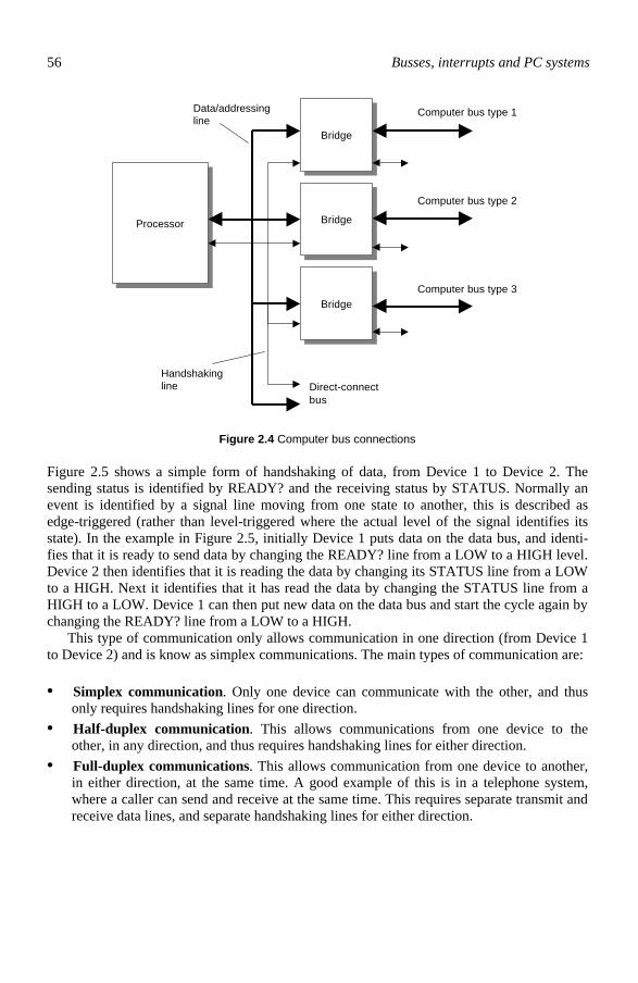
56 Busses, interrupts and PC systems
ProcessorProcessor
BridgeBridge
BridgeBridge
BridgeBridge
Computer bus type 1
Computer bus type 2
Computer bus type 3
Data/addressingline
Handshakingline Direct-connect
bus
Figure 2.4 Computer bus connections
Figure 2.5 shows a simple form of handshaking of data, from Device 1 to Device 2. The sending status is identified by READY? and the receiving status by STATUS. Normally an event is identified by a signal line moving from one state to another, this is described as edge-triggered (rather than level-triggered where the actual level of the signal identifies its state). In the example in Figure 2.5, initially Device 1 puts data on the data bus, and identi-fies that it is ready to send data by changing the READY? line from a LOW to a HIGH level. Device 2 then identifies that it is reading the data by changing its STATUS line from a LOW to a HIGH. Next it identifies that it has read the data by changing the STATUS line from a HIGH to a LOW. Device 1 can then put new data on the data bus and start the cycle again by changing the READY? line from a LOW to a HIGH. This type of communication only allows communication in one direction (from Device 1 to Device 2) and is know as simplex communications. The main types of communication are:
• Simplex communication. Only one device can communicate with the other, and thus only requires handshaking lines for one direction.
• Half-duplex communication. This allows communications from one device to the other, in any direction, and thus requires handshaking lines for either direction.
• Full-duplex communications. This allows communication from one device to another, in either direction, at the same time. A good example of this is in a telephone system, where a caller can send and receive at the same time. This requires separate transmit and receive data lines, and separate handshaking lines for either direction.

Computer busses 57
Device1
READY?
STATUS Device2
DATA
READY?
STATUS
Device 1 wants tosend data to Device 2
Device 2 is not busy
Device 2 is busy
Device 2 hasread the data
LOW
HIGHLOW
HIGH
Figure 2.5 Simple handshaking of data
Control lines
Control lines define the operation of the data transaction, such as:
• Data flow direction – this identifies that data is either being read from a device or writ-ten to a device.
• Memory addressing type – this is typically either by identifying that the address access is direct memory accessing or indirect memory access. This identifies that the address on the bus is either a real memory location or is an address tag.
• Device arbitration – this identifies which device has control of the bus, and is typically used when there are many devices connected to a common bus, and any of the devices are allowed to communicate with any other of the devices on the bus.
2.1.4 Cables
The cable type used to transmit the data over the bus depends on several parameters, includ-ing: • The signal bandwidth. • The reliability of the cable. • The maximum length between nodes. • The possibility of electrical hazards. • Power loss in the cables.

58 Busses, interrupts and PC systems
• Tolerance to harsh conditions. • Expense and general availability of the cable. • Ease of connection and maintenance. • Ease of running cables, and so on. The main types of cables used are standard copper cable, unshielded twisted-pair copper (UTP), shielded twisted-pair cable (STP), coaxial and fibre optic. Twisted-pair and coaxial cables transmit electric signals, whereas fibre optic cables transmit light pulses. Twisted-pair cables are not shielded and thus interfere with nearby cables. Public telephone lines generally use twisted-pair cables. In LANs they are generally used up to bit rates of 10 Mbps and with maximum lengths of 100 m. Coaxial cable has a grounded metal sheath around the signal conductor. This limits the amount of interference between cables and thus allows higher data rates. Typically, they are used at bit rates of 100 Mbps for maximum lengths of 1 km. The highest specification of the three cables is fibre optic. This type of cable allows ex-tremely high bit rates over long distances. Fibre optic cables do not interfere with nearby cables and give greater security, give more protection from electrical damage by external equipment and greater resistance to harsh environments; they are also safer in hazardous en-vironments.
Cable characteristics
The main characteristics of cables are attenuation, cross-talk and characteristic impedance. Attenuation defines the reduction in the signal strength at a given frequency for a defined distance. It is normally defined in dB/100 m, which is the attenuation (in dB) for 100 m. An attenuation of 3 dB/100 m gives a signal voltage reduction of 0.5 for every 100 m. Table 2.2 lists some attenuation rates and equivalent voltage ratios; they are illustrated in Figure 2.6. Attenuation is given by
dB log20nAttenuatioout
in10
=
V
V
For example if the input voltage to a cable is 10 V and the voltage at the other end is only 7 V, then the attenuation is calculated as
dB 3.1 7
10log20nAttenuatio 10 =
=
Coaxial cables have an inner core separated from an outer shield by a dielectric. They have an accurate characteristic impedance (which reduces reflections), and because they are shielded they have very low cross-talk levels. They tend also to have very low attenuation, (such as 1.2 dB at 4 MHz), with a relatively flat response. UTPs (unshielded twisted-pair cables) have either solid cores (for long cable runs) or are stranded patch cables (for shorts run, such as connecting to workstations, patch panels, and so on). Solid cables should not be flexed, bent or twisted repeatedly, whereas stranded cable can be flexed without damaging the cable. Coaxial cables use BNC connectors while UTP cables use either the RJ-11 (small
Calculation of attenuation from input and output voltages

Computer busses 59
connector which is used to connect the handset to the telephone) or the RJ-45 (larger connec-tor which is typically used in networked applications to connect a network adapter to a net-work hub). The characteristic impedance of a cable and its connectors are important, as all parts of the transmission system need to be matched to the same impedance. This impedance is nor-mally classified as the characteristic impedance of the cable. Any differences in the matching result in a reduction of signal power and produce signal reflections (or ghosting). Cross-talk is important as it defines the amount of signal that crosses from one signal path to another. This causes some of the transmitted signal to be received back where it was transmitted. Capacitance (pF/100 m) defines the amount of distortion in the signal caused by each signal pair. The lower the capacitance value, the lower the distortion.
Table 2.2 Attenuation rates as a ratio
dB Ratio dB Ratio dB Ratio
0 1.000 10 0.316 60 0.001
1 0.891 15 0.178 65 0.000 6
2 0.794 20 0.100 70 0.000 3
3 0.708 25 0.056 75 0.000 2
4 0.631 30 0.032 80 0.000 1
5 0.562 35 0.018 85 0.000 06
6 0.501 40 0.010 90 0.000 03
7 0.447 45 0.005 6 95 0.000 02
8 0.398 50 0.003 2 100 0.000 01
9 0.355 55 0.001 8
0.0001
0.001
0.01
0.1
1
0 10 20 30 40 50 60
Attenuation (dB)
Sig
nal r
atio
Figure 2.6 Signal ratio related to attenuation

60 Busses, interrupts and PC systems
Typical cables used are: • Coaxial cable – cables with an inner core and a conducting shield having characteristic
impedance of either 75 Ω for TV signal or 50 Ω for other types. • Cat-3 UTP cable – level 3 cables have non-twisted-pair cores with a characteristic im-
pedance of 100 Ω (±15 Ω) and a capacitance of 59 pF/m. Conductor resistance is around 9. 2 Ω/100 m.
• Cat-5 UTP cable – level 5 cables have twisted-pair cores with a characteristic impedance of 100 Ω (±15 Ω) and a capacitance of 45.9 pF/m. Conductor resistance is around 9 Ω/100 m.
The Electrical Industries Association (EIA) has defined five main types of cables. Levels 1 and 2 are used for voice and low-speed communications (up to 4 Mbps). Level 3 is designed for LAN data transmission up to 16 Mbps and level 4 is designed for speeds up to 20 Mbps. Level 5 cables, have the highest specification of the UTP cables and allow data speeds of up to 100 Mbps. The main EIA specification on these types of cables is EIA/TIA568 and the ISO standard is ISO/IEC11801. Table 2.3 gives typical attenuation rates (dB/100 m) for Cat-3, Cat-4 and Cat-5 cables. Notice that the attenuation rates for Cat-4 and Cat-5 are approximately the same. These two types of cable have lower attenuation rates than equivalent Cat-3 cables. Notice that the at-tenuation of the cable increases as the frequency increases. This is due to several factors, such as the skin effect, where the electrical current in the conductors becomes concentrated around the outside of the conductor, and the fact that the insulation (or dielectric) between the conductors actually starts to conduct as the frequency increases. The Cat-3 cable produces considerable attenuation over a distance of 100 m. The table shows that the signal ratio of the output to the input at 1 MHz, will be 0.76 (2.39 dB), then, at 4 MHz it is 0.55 (5.24 dB), until at 16 MHz it is 0.26. This differing attenuation at different frequencies produces not just a reduction in the signal strength but also distorts the signal (because each frequency is affected differently by the cable. Cat-4 and Cat-5 cables also pro-duce distortion but their effects will be lessened because attenuation characteristics have flat-ter shapes. Table 2.4 gives typical near-end cross-talk rates (dB/100 m) for Cat-3, Cat-4 and Cat-5 cables. The higher the figure, the smaller the cross-talk. Notice that Cat-3 cables have the most cross-talk and Cat-5 have the least, for any given frequency. Notice also that the cross talk increases as the frequency of the signal increases. Thus, high-frequency signals have more cross-talk than lower-frequency signals.
Table 2.3 Attenuation rates (dB/100 m) for Cat-3, Cat-4 and Cat-5 cable
Frequency (MHz) Attenuation rate (dB/100 m)
Cat-3 Cat-4 Cat-5
1 2.39 1.96 2.63
4 5.24 3.93 4.26
10 8.85 6.56 6.56
16 11.8 8.2 8.2

Computer busses 61
Table 2.4 Near-end cross-talk (dB/100 m) for Cat-3, Cat-4 and Cat-5 cable
Near end cross-talk (dB/100 m) Frequency (MHz)
Cat-3 Cat-4 Cat-5
1 13.45 18.36 21.65
4 10.49 15.41 18.04
10 8.52 13.45 15.41
16 7.54 12.46 14.17
2.2 Interrupts
An interrupt allows a program or an external device to interrupt the execution of a program. The generation of an interrupt can occur by hardware (hardware interrupt) or software (soft-ware interrupt). When an interrupt occurs an interrupt service routine (ISR) is called. For a hardware interrupt the ISR then communicates with the device and processes any data. When it has finished the program execution returns to the original program. A software interrupt causes the program to interrupt its execution and goes to an interrupt service routine. Typical software interrupts include reading a key from the keyboard, outputting text to the screen and reading the current date and time. The operating system must respond to interrupts from external devices, as illustrated in Figure 2.7.
InterruptcontrollerInterruptcontroller
Hardware interrupts
InterruptServiceRoutine
(ISR)
InterruptServiceRoutine
(ISR)
Software interrupts
Operatingsystem
Program requestsProgram requests
InterruptcontrollerInterruptcontroller
Hardware interrupts
InterruptServiceRoutine
(ISR)
InterruptServiceRoutine
(ISR)
Software interrupts
Operatingsystem
Program requestsProgram requests
Figure 2.7 Interrupt service routine

62 Busses, interrupts and PC systems
2.2.1 Software interrupts
BIOS and the operating system
The Basic Input/Output System (BIOS) communicates directly with the hardware of the computer. It consists of a set of programs which interface with devices such as keyboards, displays, printers, serial ports and disk drives. These programs allow the user to write appli-cation programs that contain calls to these functions, without having to worry about control-ling them or which type of equipment is being used. Without BIOS, the computer system would simply consist of a bundle of wires and electronic devices. There are two main parts to BIOS. The first is the part permanently stored in a ROM (the ROM BIOS). It is this part that starts the computer (or bootstap) and contains programs which communicate with resident devices. The second stage is loaded when the operating system is started. This part is non-permanent. An operating system allows the user to access the hardware in an easy-to-use manner. It accepts commands from the keyboard and displays them to the monitor. The Disk Operating System, or DOS, gained its name from its original purpose of providing a controller for the computer to access its disk drives. The language of DOS consists of a set of commands which are entered directly by the user and are interpreted to perform file management tasks, program execution and system configuration. It makes calls to BIOS to execute these. The main functions of DOS are to run programs, copy and remove files, create directories, move within a directory structure and to list files. Microsoft Windows calls BIOS programs di-rectly.
Interrupt vectors
Interrupt vectors are addresses which inform the interrupt handler as to where to find the ISR. All interrupts are assigned a number from 0 to 255. The interrupt vectors associated with each interrupt number are stored in the lower 1024 bytes of PC memory. For example, interrupt 0 is stored from 0000:0000 to 0000:0003, interrupt 1 from 0000:0004 to 0000:0007, and so on. The first two bytes store the offset and the next two store the seg-ment address. Each interrupt number is assigned a predetermined task, as outlined in Table 2.5. An interrupt can be generated either by external hardware, software, or by the processor. Interrupts 0, 1, 3, 4, 6 and 7 are generated by the processor. Interrupts from 8 to 15 and inter-rupt 2 are generated by external hardware. These get the attention of the processor by activat-ing a interrupt request (IRQ) line. The IRQ0 line connects to the system timer, the keyboard to IRQ1, and so on. Most other interrupts are generated by software.
Processor interrupts
The processor-generated interrupts normally occur either when a program causes a certain type of error or if it is being used in a debug mode. In the debug mode the program can be made to break from its execution when a break-point occurs. This allows the user to test the status of the computer. It can also be forced to step through a program one operation at a time (single-step mode).

Computer busses 63
Table 2.5 Interrupt handling (codes followed by ‘h’ are in hexadecimal)
Interrupt Name Generated by 00 (00h) Divide error processor 01 (00h) Single step processor 02 (02h) Non-maskable interrupt external equipment 03 (03h) Breakpoint processor 04 (04h) Overflow processor 05 (05h) Print screen Shift-Print screen key stroke 06 (06h) Reserved processor 07 (07h) Reserved processor 08 (08h) System timer hardware via IRQ0 09 (09h) Keyboard hardware via IRQ1 10 (0Ah) Reserved hardware via IRQ2 11 (0Bh) Serial communications (COM2) hardware via IRQ3 12 (0Ch) Serial communications (COM1) hardware via IRQ4 13 (0Dh) Reserved hardware via IRQ5 14 (0Eh) Floppy disk controller hardware via IRQ6 15 (0Fh) Parallel printer hardware via IRQ7 16 (10h) BIOS – Video access software 17 (11h) BIOS – Equipment check software 18 (12h) BIOS – Memory size software 19 (13h) BIOS – Disk operations software 20 (14h) BIOS – Serial communications software 22 (16h) BIOS – Keyboard software 23 (17h) BIOS – Printer software 25 (19h) BIOS – Reboot software 26 (1Ah) BIOS – Time of day software 28 (1Ch) BIOS – Ticker timer software 33 (21h) DOS – DOS services software 39 (27h) DOS – Terminate and stay resident software
2.2.2 Hardware interrupts
Computer systems either use polling or interrupt-driven software to service external equip-ment. With polling the computer continually monitors a status line and waits for it to become active, whereas an interrupt-driven device sends an interrupt request to the computer, which is then serviced by an interrupt service routine (ISR). Interrupt-driven devices are normally better in that the computer is thus free to do other things, whereas polling slows the system down as it must continually monitor the external device. Polling can also cause problems in that a device may be ready to send data and the computer is not watching the status line at that point. Figure 2.8 illustrates polling and interrupt-driven devices. The generation of an interrupt can occur by hardware or software, as illustrated in Figure 2.9. If a device wishes to interrupt the processor, it informs the programmable interrupt con-troller (PIC). The PIC then decides whether it should interrupt the processor. If there is a processor interrupt then the processor reads the PIC to determine which device caused the interrupt. Then, depending on the device that caused the interrupt, a call to an ISR is made. The ISR then communicates with the device and processes any data. When it has finished the program execution returns to the original program. A software interrupt causes the program to interrupt its execution and goes to an interrupt service routine. Typical software interrupts include reading a key from the keyboard, output-

64 Busses, interrupts and PC systems
ting text to the screen and reading the current date and time. Hardware interrupts allow external devices to gain the attention of the processor. Depending on the type of interrupt the processor leaves the current program and goes to a special program called an interrupt service routine (ISR). This program communicates with the device and processes any data. After it has completed its task then program execution returns to the program that was running before the interrupt occurred. Examples of interrupts include the processing of keys from a keyboard and data from a sound card. As previously mentioned, a device informs the processor that it wants to interrupt it by setting an interrupt line on the PC. Then, depending on the device that caused the interrupt, a call to an ISR is made. Each PIC allows access to eight interrupt request lines. Most PCs use two PICs which gives access to 16 interrupt lines.
Processor
Interrupt-driven:external devicesinterrupt the processorwhen they wish to communicate
Polling:processor pollsdevices to see if theywish to communicate
Externaldevice
Processor
Externaldevice
Figure 2.8 Polling or interrupt-driven communications
Interruptcontroller
Interruptcontroller
Processor
Interruptserviceroutines
INT
InterruptlinesSoftware
interrupt
Keyboard (IRQ1) Mouse (IRQ12)
Modem (IRQ4)
Printer (IRQ7)
Floppy (IRQ6)
Serial port (IRQ3/4)
Figure 2.9 Interrupt handling

Computer busses 65
Interrupt vectors
Each device that requires to be ‘interrupt-driven’ is assigned an IRQ (interrupt request) line. Each IRQ is active high. The first eight (IRQ0–IRQ7) map into interrupts 8 to 15 (08h–0Fh) and the next eight (IRQ8–IRQ15) into interrupts 112 to 119 (70h–77h). Table 2.6 outlines the usage of each of these interrupts. When IRQ0 is made active, the ISR corresponds to interrupt vector 8. IRQ0 normally connects to the system timer, the keyboard to IRQ1, and so on. The standard set-up of these interrupts is illustrated in Figure 2.10. The system timer interrupts the processor 18.2 times per second and is used to update the system time. When the keyboard has data, it interrupts the processor with the IRQ1 line.
System timer
Keyboard
Serial port
(COM2:)
Serial port
(COM1:)
Floppy disk
controller
Parallel port
(LPT2:)
Parallel port
(LPT1:)
IRQ0
IRQ1
IRQ3
IRQ4
IRQ5
IRQ6
IRQ7
Interruptserviceroutine
Programmableinterruptcontroller (PIC)
ProcessorINT
Figure 2.10 Standard usage of IRQ lines
Table 2.6 Interrupt handling
Interrupt Name Generated by 08 (08h) System timer IRQ0 09 (09h) Keyboard IRQ1 10 (0Ah) Reserved IRQ2 11 (0Bh) Serial communications (COM2:) IRQ3 12 (0Ch) Serial communications (COM1:) IRQ4 13 (0Dh) Parallel port (LPT2:) IRQ5 14 (0Eh) Floppy disk controller IRQ6 15 (0Fh) Parallel printer (LPT1:) IRQ7 112 (70h) Real-time clock IRQ8 113 (71h) Redirection of IRQ2 IRQ9 114 (72h) Reserved IRQ10 115 (73h) Reserved IRQ11 116 (74h) Reserved IRQ12 117 (75h) Math co-processor IRQ13 118 (76h) Hard disk controller IRQ14 119 (77h) Reserved IRQ15
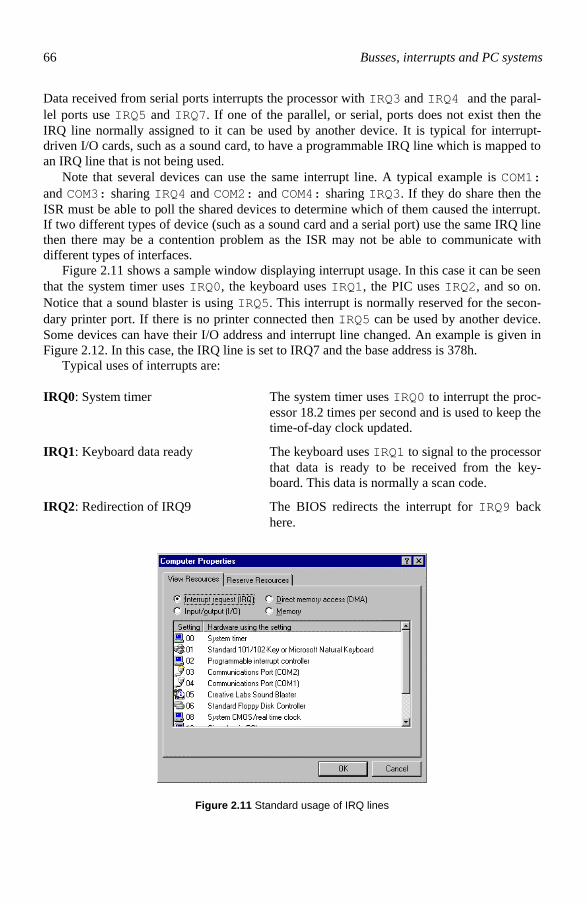
66 Busses, interrupts and PC systems
Data received from serial ports interrupts the processor with IRQ3 and IRQ4 and the paral-lel ports use IRQ5 and IRQ7. If one of the parallel, or serial, ports does not exist then the IRQ line normally assigned to it can be used by another device. It is typical for interrupt-driven I/O cards, such as a sound card, to have a programmable IRQ line which is mapped to an IRQ line that is not being used. Note that several devices can use the same interrupt line. A typical example is COM1: and COM3: sharing IRQ4 and COM2: and COM4: sharing IRQ3. If they do share then the ISR must be able to poll the shared devices to determine which of them caused the interrupt. If two different types of device (such as a sound card and a serial port) use the same IRQ line then there may be a contention problem as the ISR may not be able to communicate with different types of interfaces. Figure 2.11 shows a sample window displaying interrupt usage. In this case it can be seen that the system timer uses IRQ0, the keyboard uses IRQ1, the PIC uses IRQ2, and so on. Notice that a sound blaster is using IRQ5. This interrupt is normally reserved for the secon-dary printer port. If there is no printer connected then IRQ5 can be used by another device. Some devices can have their I/O address and interrupt line changed. An example is given in Figure 2.12. In this case, the IRQ line is set to IRQ7 and the base address is 378h. Typical uses of interrupts are: IRQ0: System timer The system timer uses IRQ0 to interrupt the proc-
essor 18.2 times per second and is used to keep the time-of-day clock updated.
IRQ1: Keyboard data ready The keyboard uses IRQ1 to signal to the processor that data is ready to be received from the key-board. This data is normally a scan code.
IRQ2: Redirection of IRQ9 The BIOS redirects the interrupt for IRQ9 back here.
Figure 2.11 Standard usage of IRQ lines

Computer busses 67
Figure 2.12 Standard set-up of IRQ lines
IRQ3: Secondary serial port (COM2:) The secondary serial port (COM2:) uses IRQ3 to interrupt the processor. Typically, COM3: to COM8: also use it, although COM3: may use IRQ4.
IRQ4: Primary serial port (COM1:) The primary serial port (COM1:) uses IRQ4 to interrupt the processor. Typically, COM3: also uses it.
IRQ5: Secondary parallel port (LPT2:) On older PCs the IRQ5 line was used by the fixed disk. On newer systems the secondary parallel port uses it. Typically, it is used by a sound card on PCs which have no secondary parallel port con-nected.
IRQ6: Floppy disk controller The floppy disk controller activates the IRQ6 line on completion of a disk operation.
IRQ7: Primary parallel port (LPT1:) Printers (or other parallel devices) activate the IRQ7 line when they become active. As with IRQ5 it may be used by another device, if there are no other devices connected to this line.
IRQ9 Redirected to IRQ2 service routine.

68 Busses, interrupts and PC systems
Programmable interrupt controller (PIC)
The PC uses the 8259 PIC to control hardware-generated interrupts. It is known as a pro-grammable interrupt controller and has eight input interrupt request lines and an output line to secondary PIC are then assigned IRQ lines of IRQ8 to IRQ15. This set-up is shown in Figure 2.13. When an interrupt occurs on any of these lines it is sensed by the processor on interrupt the processor. Originally, PCs only had one PIC and eight IRQ lines (IRQ0-IRQ7). Modern PCs can use up to 15 IRQ lines which are set up by connecting a secondary PIC in-terrupt request output line to the IRQ2 line of the primary PIC. The interrupt lines on the IRQ2 line. The processor then interrogates the primary and secondary PIC for the interrupt line which caused the interrupt. The primary and secondary PICs are programmed via port addresses 20h and 21h, as given in Table 2.7. The operation of the PIC is programmed using registers. The IRQ input lines are either configured as level-sensitive or edge-triggered interrupt. With edge-triggered interrupts, a change from a low to a high on the IRQ line causes the interrupt. A level-sensitive interrupt occurs when the IRQ line is high. Most devices generate edge-triggered interrupts.
IRQ0
IRQ1
IRQ2
IRQ3
IRQ4
IRQ5
IRQ6
IRQ7
PIC 1
PIC 2
Interruptrequest
IRQ8
IRQ9
IRQ10
IRQ11
IRQ12
IRQ13
IRQ14
IRQ15
Figure 2.13 PC PIC connections
In the IMR an interrupt line is enabled by setting the assigned bit to a 0 (zero). This allows the interrupt line to interrupt the processor. Figure 2.14 shows the bit definitions of the IMR. For example, if bit 0 is set to a zero then the system timer on IRQ0 is enabled.
Table 2.7 Interrupt port addresses
Port address Name Description 20h Interrupt control register
(ICR) Controls interrupts and signifies the end of an interrupt
21h Interrupt mask register (IMR)
Used to enable and disable interrupt lines

Computer busses 69
IRQ6 IRQ4 IRQ2 IRQ0
IRQ7 IRQ5 IRQ3 IRQ1
IMR (21h)
0 – enable
1 – disable
0 – enable
1 – disable
0 – enable
1 – disable
0 – enable
1 – disable
0 – enable
1 – disable
0 – enable
1 – disable
0 – enable
1 – disable
0 – enable
1 – disable
Figure 2.14 Interrupt mask register bit definitions
In the example code given next the lines IRQ0, IRQ1 and IRQ6 are allowed to interrupt the processor, whereas, IRQ2, IRQ3, IRQ4 and IRQ7 are disabled: _outp(0x21)=0xBC; /* 1011 1100 enable disk (bit 6), keyboard (1) and timer (0) interrupts */ When an interrupt occurs all other interrupts are disabled and no other device can interrupt the processor. Interrupts are enabled again by setting the EOI bit on the interrupt control port, as shown in Figure 2.15. The following code enables interrupts: _outp(0x20,0x20); /* EOI command */
EOI signal
1 – end of interrupt
Interrupt request
level to be acted on
0 – 000
1 – 001
2 – 010
and so on.
ICR (20h) 0 00
Figure 2.15 Interrupt control register bit definitions
2.3 Interfacing
There are two main methods of communicating with external equipment, either they are mapped into the physical memory and given a real address on the address bus (memory mapped I/O) or they are mapped into a special area of input/output memory (isolated I/O).

70 Busses, interrupts and PC systems
Figure 2.16 shows the two methods. Devices mapped into memory are accessed by reading or writing to the physical address. Isolated I/O provides ports which are gateways between the interface device and the processor. They are isolated from the system using a buffering system and are accessed by four machine code instructions. The IN instruction inputs a byte, or a word, and the OUT instruction outputs a byte, or a word. A high-level compiler interprets the equivalent high-level functions and produces machine code which uses these instructions.
Interface deviceaccessed directlyin memory
I/O ports
Interfacehardware
Interface deviceaccessed via portswith IN and OUTassembly languageinstructions
Interfacedevice
Devicebuffering
Pascalprogram
Interfacedevice
Figure 2.16 Memory mapping or isolated interfacing
2.3.1 Interfacing with memory
The 80x86 processor interfaces with memory through a bus controller, as shown in Figure 2.17. This device interprets the microprocessor signals and generates the required memory signals. Two main output lines differentiate between a read or a write operation ( R / W ) and between direct and isolated memory access (M / IO ). The R / W line is low when data is being written to memory and high when data is being read. When M / IO is high, direct memory access is selected and when low, the isolated memory is selected.
2.3.2 Memory mapped I/O
Interface devices can map directly onto the system address and data bus. In a PC-compatible system the address bus is 20 bits wide, from address 00000h to FFFFFh (1 MB). If the PC is being used in an enhanced mode (such as with Microsoft Windows) it can access the area of memory above 1 MB. If it uses 16-bit software (such as Microsoft Windows 3.1) then it can address up to 16 MB of physical memory, from 000000h to FFFFFFh. If it uses 32-bit software (such as Microsoft Windows 95/98/NT/2000) then the software can address up to 4 GB of physical memory, from 00000000h to FFFFFFFFh. Figure 2.18 gives a typical memory allocation.

Computer busses 71
M/IO
R/W
Memory
mapped
I/O
Isolated
I/O
Read/ Write
Memory/Isolated
Address bus
Data bus
Bus controller
Microprocessor
Interface devices
Figure 2.17 Access memory mapped and isolated I/O
Extendedmemory
Extendedmemory
Video graphicsText display
Application programs(640 KB)
Interrupt vectorsBIOS
00000000h
00000600h
0009FFFFh (640 KB)
000FFFFFh (1 MB)
00FFFFFFh (16 MB)
FFFFFFFFh (4 GB)
Figure 2.18 Typical PC memory map
2.3.3 Isolated I/O
Devices are not normally connected directly onto the address and data bus of the computer because they may use part of the memory that a program uses or they could cause a hardware fault. On modern PCs only the graphics adaptor is mapped directly into memory, the rest communicate through a specially reserved area of memory, known as isolated I/O memory. Isolated I/O uses 16-bit addressing from 0000h to FFFFh, thus up to 64 KB of memory can be mapped. Figure 2.19 shows an example for a computer in the range from 0000h to 0064h and Figure 2.20 shows from 0378h to 03FFh. It can be seen from Figure 2.19 that the keyboard maps into addresses 0060h and 0064h, the speaker maps to address 0061h

72 Busses, interrupts and PC systems
and the system timer between 0040h and 0043h. Table 2.8 shows the typical uses of the isolated memory area.
Figure 2.19 Example I/O memory map from 0000h to 0064h
Figure 2.20 Example I/O memory map from 0378h to 03FFh

Computer busses 73
Table 2.8 Typical isolated I/O memory map
Address Device 000h-01Fh DMA controller 020h-021h Programmable interrupt controller 040h-05Fh Counter/Timer 060h-07Fh Digital I/O 080h-09Fh DMA controller 0A0h-0BFh NMI reset 0C0h-0DFh DMA controller 0E0h-0FFh Math coprocessor 170h-178h Hard disk (Secondary IDE drive or CD-ROM drive) 1F0h-1F8h Hard disk (Primary IDE drive) 200h-20Fh Game I/O adapter 210h-217h Expansion unit 278h-27Fh Second parallel port (LPT2:) 2F8h-2FFh Second serial port (COM2:) 300h-31Fh Prototype card 378h-37Fh Primary parallel port (LPT1:) 380h-38Ch SDLC interface 3A0h-3AFh Primary binary synchronous port 3B0h-3BFh Graphics adapter 3C0h-3DFh Graphics adapter 3F0h-3F7h Floppy disk controller 3F8h-3FFh Primary serial port (COM1:)
Inputting a byte from an I/O port
The assembly language command to input a byte is IN AL,DX
where DX is the data register which contains the address of the input port. The 8-bit value loaded from this address is put into the register A
For Turbo/Borland C the equivalent function is inportb(). Its general syntax is as fol-lows: value=inportb(PORTADDRESS);
where PORTADDRESS is the address of the input port and value is loaded with the 8-bit value from this address. This function is prototyped in the header file dos.h.
For Turbo Pascal the equivalent is accessed via the port[] array. Its general syntax is as follows: value:=port[PORTADDRESS];
where PORTADDRESS is the address of the input port and value the 8-bit value at this address. To gain access to this function the statement uses dos requires to be placed near the top of the program.

74 Busses, interrupts and PC systems
Microsoft C++ uses the equivalent _inp() function (which is prototyped in conio.h).
Inputting a word from a port
The assembly language command to input a word is IN AX,DX
where DX is the data register which contains the address of the input port. The 16-bit value loaded from this address is put into the register AX.
For Turbo/Borland C the equivalent function is inport(). Its general syntax is as follows: value=inport(PORTADDRESS);
where PORTADDRESS is the address of the input port and value is loaded with the 16-bit value at this address. This function is prototyped in the header file dos.h.
For Turbo Pascal the equivalent is accessed via the portw[] array. Its general syntax is as follows: value:=portw[PORTADDRESS];
where PORTADDRESS is the address of the input port and value is the 16-bit value at this address. To gain access to this function the statement uses dos requires to be placed near the top of the program.
Microsoft C++ uses the equivalent _inpw() function (which is prototyped in conio.h).
Outputting a byte to an I/O port
The assembly language command to output a byte is OUT DX,AL
where DX is the data register which contains the address of the output port. The 8-bit value sent to this address is stored in register AL.
For Turbo/Borland C the equivalent function is outportb(). Its general syntax is as fol-lows: outportb(PORTADDRESS,value);
where PORTADDRESS is the address of the output port and value is the 8-bit value to be sent to this address. This function is prototyped in the header file dos.h.
For Turbo Pascal the equivalent is accessed via the port[] array. Its general syntax is as follows:

Computer busses 75
port[PORTADDRESS]:=value;
where PORTADDRESS is the address of the output port and value is the 8-bit value to be sent to that address. To gain access to this function the statement uses dos requires to be placed near the top of the program.
Microsoft C++ uses the equivalent _outp() function (which is prototyped in conio.h).
Outputting a word
The assembly language command to input a byte is: OUT DX,AX
where DX is the data register which contains the address of the output port. The 16-bit value sent to this address is stored in register AX.
For Turbo/Borland C the equivalent function is outport(). Its general syntax is as fol-lows: outport(PORTADDRESS,value);
where PORTADDRESS is the address of the output port and value is the 16-bit value to be sent to that address. This function is prototyped in the header file dos.h.
For Turbo Pascal the equivalent is accessed via the port[] array. Its general syntax is as follows: portw[PORTADDRESS]:=value;
where PORTADDRESS is the address of the output port and value is the 16-bit value to be sent to that address. To gain access to this function the statement uses dos requires to be placed near the top of the program.
Microsoft C++ uses the equivalent _outp() function (which is prototyped in conio.h).
In-line assembly language
Most modern C++ development systems use an inline assembler which allows assembly lan-guage code to be embedded with C++ code. This code can use any C variable or function name that is in scope. The __asm keyword invokes the inline assembler and can appear wher-ever a C statement is legal. The following code is a simple __asm block enclosed in braces. __asm /* Initialize serial port */ mov dx,0x01; /* COM2: */ mov al,0xD2; /* serial port parameters */ mov ah,0x0; /* initialize serial port */ int 14h; line_status=ah; modem_status=al;

76 Busses, interrupts and PC systems
Note these statements can also be inserted after the __asm keyword, such as: __asm mov dx,0x01; /* COM2: */ __asm mov al,0xD2; /* serial port parameters */ __asm mov ah,0x0; /* initialize serial port */ __asm int 14h; __asm line_status=ah; __asm modem_status=al;
2.4 PC Systems
In selecting a PC many different components must be considered, especially in the way that they connect. Figure 2.21 outlines some of the component parts and the decisions that have to be made on each component.
+ Processor:TypeCache size (Level-1)Clock speed
+ Internal Busses:ISAPCIIDE
+
+ Graphics:Type (Chipset)Processing (3D/Accelerator)Memory (Local memory)
AGP
+ External Busses:Parallel PortSerial PortSCSIUSB
+ Memory:Type (DIMM/SDRAM/SIMM)Cache (Level-2)Speed
+Type (Optical/Hard disk/Floppy disk)Interface (SCSI/IDE)Capacity (KB/MB/GB)
Storage:
Socket (SEC/Socket) Interface (PCI/AGP)
Figure 2.21 PC components
The Top 5 things that affect the general performance of a PC (in ranked order) are: 1. Processor. The type of the processor, its speed, its socket (which helps in upgrading in
the future), its interface to Level-2 cache, and so on. Additionally, MMXTM, (which is an Intel trademark, but many read it as MultiMedia eXtension) can speed-up multi-media applications.
2. Local Memory. Most operating systems can run multiple programs, each of which re-quire their own memory space. When the system runs out of electronic memory (local memory), it uses the hard disk for an extra storage (to create a virtual memory). Hard disk accesses are much slower than electronic memory, thus the system is severely slowed down if there is a lack of local electronic memory. Most modern operating sys-

Computer busses 77
tems require a great deal of local electronic memory to operate. 3. Graphics adaptor. The graphics adaptor can be a major limiting factor on the perform-
ance of a system. New interfaces, such as AGP, considerably speed-up graphics per-formance. Another limiting factor is the amount of local memory on the graphics adap-tor. The more memory, the higher the resolution that can be used, and the more colours that can be displayed. AGP is overcoming this limiting factor, as it allows the main elec-tronic memory to be used to store graphics images.
4. Cache capacity. Cache memory has caused a great increase in the performance of a system. If a cache controller makes a correct guess, the processor merely has to examine the contents of the cache to get the required information. A level-1 cache is the fastest and is typically connected directly to the processor (normally inside the processor pack-age), and the level-2 cache is on the motherboard.
5. Hard disk capacity/interface. The hard disk typically has an affect on the running of a program, as the program and its component parts must be loaded from the disk. The in-terface is thus extremely important as it defines the maximum data rate. SCSI has fast modes which give up to 40 MB/s, while IDE gives a maximum rate of 33 MB/s. The ca-pacity of the disk also can lead to problems as the system can use unused disk capacity of a virtual memory capacity.
Obviously, applications that are more specific will be affected by other factors, such as: • Internet access. Affected mainly by the network connection (especially if a modem is
used). • CD-ROM access. Affected by the interface to the CD-ROM. • Modelling software. Affected by mathematical processing. • 3D game playing. Affected mainly by the graphics adaptor and graphics processing
(and possibly the network connection, if playing over a network).
2.8 Practical PC system
At one time PCs were crammed full of microchips, wires and connectors. These days they tend to be based on just a few microchips, and contain very few interconnecting wires. The main reason for this is that much of the functionality of the PC has been integrated into sev-eral key devices. In the future, PCs may only require one or two devices to make them oper-ate. The architecture of the PC has changed over the past few years. It is now mainly based on the PCI bus. Figure 2.22 shows the architecture of a modern PC. The system controller is the real heart of the PC, as it transfers data to and from the processor to the rest of the system. Bridges are used to connect one type of bus to another. There are two main bridges: the sys-tem controller (the north bridge), and the bus bridge (the south bridge).

78 Busses, interrupts and PC systems
ProcessorProcessor SystemController
SystemController
DRAMmemory
DRAMmemory
SRAM cachememory
SRAM cachememory
Busbridge
Busbridge
PCI bus connections (typically up to 5 devices)
ISA bus IDE bus USB bus
Databus
Addressbus
DRAMaddresses
DRAMData bus
SRAM tag address
Motherboard clockspeed
Processor clockspeed
LocalSRAMcache
LocalSRAMcache
Add
ress
bus
Dat
abu
s
Differing clockspeeds
Figure 2.22 Local bus architecture
An example PC motherboard is illustrated in Figure 2.23. The main components are: • Processor. The processor is typically a Pentium processor, which has a SEC (single-
edge connector) or fits into a socket. The processor can run at a faster rate than the rest of the motherboard (called clock multiplication). Typically, the motherboard runs at 50MHz, and the clock rate is multiplied by a given factor, such as 500MHz (for a ×10 clock multiplier).
• System controller. Controls the interface between the processor, memory and the PCI bus.
• PCI/ISA/IDE Xcelerated Controller. Controls the interface between the PCI bus and the ISA, USB and IDE busses.
• I/O controller. Controls the interface between the ISA and the other busses, such as the parallel bus, serial bus, floppy disk drive, keyboard, mouse, and infrared transmission.
• DIMM sockets. This connects to the main memory of the computer. Typically it uses either EDO DRAM and SDRAM (Synchronous DRAM). SDRAM transfers data faster than EDO DRAM as its uses the clock rate of the processor, rather than the clock rate of the motherboard.
• Flash memory. Used to store the program which starts the computer up (the boot proc-ess).
• PCI connectors. Used to connect to PCI-based interface adaptors, such as a network card, sound card, and so on.
• ISA connectors. Used to connect to ISA-based interface adaptors, such as a sound cards.
• IDE connectors. Used to connect to hard disks or CD-ROM drives. Up to two drives

Computer busses 79
can connect to each connector (IDE0 or IDE1) as a master or a slave. Thus, the PC can support up to four disk drives on the IDE bus.
• TV out socket. Used to provide an output which will interface to a TV, using either PAL (for the UK) or NSTC (for the US).
• Level-2 cache (SRAM). Used to store information from DRAM memory. • Video memory. Used to store video information. • Graphics controller. Used to control the graphics output. • Audio codec. Used to process audio data.
ISA connectors
PCI connectors
DIMMsockets
IDEconnectors
Graphicscontroller
82430TXSystemController
82430TXPCI/ISA/IDEXcelerator (PIIX4)
Level 2 cacheSRAM
Audiocodec
Audio(OP4-ML)
Pentiumprocessor
TV-outdevice
Videomemory
Flashmemorydevice
PC87307ULI/O Controller
Videocaptureprocessor
Figure 2.23 AN430TX board
2.5 Exercises
The following questions are multiple choice. Please select from a–d. 2.4.1 Which type of memory does not lose its contents when the power is withdrawn: (a) ROM (b) RAM (c) DRAM (d) SRAM 2.4.2 Which type of memory uses a single capacitor and a transistor to store a single bit
of data:

80 Busses, interrupts and PC systems
(a) EPROM (b) ERAM (c) DRAM (d) SRAM 2.4.3 Which type of memory requires its memory of be refreshed at regular intervals: (a) EPROM (b) ERAM (c) DRAM (d) SRAM 2.4.4 If a processor can operate on four bytes at a time, which is its classification: (a) 8-bit (b) 16-bit (a) 32-bit (b) 64-bit 2.4.5 Which of the following defines the amount of memory that can be accessed: (a) Address bus (b) Control lines (c) Handshaking lines (d) Data bus 2.4.6 Which of the following defines the number of bits that can be transmitted at a
time: (a) Address bus (b) Control lines (c) Handshaking lines (d) Data bus 2.4.7 Which is the maximum data throughput for a 32-bit parallel data bus with a
clocked data rate of 10 MHz: (a) 4 MB/s (b) 40 MB/s (c) 32 MB/s (d) 320 MB/s 2.4.8 Which is the maximum data throughput for a serial bus which has a bit transmis-
sion time of 69.44 µs: (a) 6944 bps (b) 9600 bps (c) 1440 bps (d) 144 00 bps 2.4.9 How much memory can be accessed with a 20-bit address bus: (a) 20 B (b) 20 KB (c) 1 MB (d) 20 MB 2.4.10 How much memory can be accessed with a 32-bit address bus: (a) 32 B (b) 32 KB (c) 1 GB (d) 32 MB 2.4.11 Which interrupt does the primary serial port of a PC (COM1:) normally use: (a) IRQ0 (b) IRQ3

Computer busses 81
(c) IRQ4 (d) IRQ7 2.4.12 Which interrupt does the secondary serial port of a PC (COM2:) normally use: (a) IRQ0 (b) IRQ3 (c) IRQ4 (d) IRQ7 2.4.13 Which interrupt does the system timer on the PC use: (a) IRQ0 (b) IRQ3 (c) IRQ4 (d) IRQ7 2.4.14 Which interrupt was used to increase the amount of interrupts from 8 to 16: (a) IRQ0 (b) IRQ1 (c) IRQ2 (d) IRQ15 2.4.15 Which interrupt is used by the keyboard: (a) IRQ0 (b) IRQ1 (c) IRQ2 (d) IRQ15 2.4.16 What does ISR stand for: (a) Interval Status Register (b) Interrupt Status Register (c) Interrupt Service Routine (d) Interrupt Standard Routine 2.4.17 How is isolated memory differentiated from memory added I/O: (a) Different address bus (b) Different data bus (c) Control line differentiates between them (Memory/Isolated) (d) There is no differentiation as they are physically the same 2.4.18 How many addresses can be accessed in the address range 0000h to FFFFh: (a) 32 768 (32 kB) (b) 65 536 (64 kB) (c) 262 144 (256 kB) (d) 1 048 576 (1 MB) 2.4.19 How much physical memory can a DOS-compatible program access: (a) 32 768 (32 kB) (b) 65 536 (64 kB) (c) 262 144 (256 kB) (d) 1 048 576 (1 MB) 2.4.20 Which address is the interrupt control port register: (a) 0002h (b) 0020h (c) 0200h (d) 2000h 2.4.21 Which is normally the base address for the primary parallel port: (a) 0378h (b) 0278h (c) 03F8h (d) 02F8h

82 Busses, interrupts and PC systems
2.4.22 Contrast the operation of polling and interrupt-driven software when interfacing to external equipment.
2.4.23 Access a PC and determine the following:
Interrupt Device connected IRQ1 IRQ3 IRQ5 IRQ7 IRQ9 IRQ11 IRQ13 IRQ15 I/O address Device connected 0060h, 0064h 0070h 0090h 00F0h 0278h 02F8h 0378h 03F8h DMA channel Device connected DMA0 DMA1 DMA2 DMA3
2.6 Notes from the author
This chapter has introduced some of the key concepts used in defining computer systems. So, what is it that differentiates one PC system from another? It is difficult to say, but basically its all about how well bolted together systems are, how compatible the parts are with the loaded software, how they organise the peripherals, and so on. The big problem though is compatibility, and compatibility is all about peripherals looking the same, that is, having the same IRQ, the same I/O address, and so on. The PC is an amazing device, and has allowed computers to move from technical special-ists to, well, anyone. However, they are also one of the most annoying of pieces of technol-ogy of all time, in terms of their software, their operating system, and their hardware. If we bought a car and it failed at least a few times every day, we would take it back and demand another one. When that failed, we would demand our money back. Or, sorry I could go on forever here, imagine a toaster that failed half way through making a piece of toast, and we had to turn the power off, and restart it. We just wouldn’t allow it. So why does the PC lead such a privileged life. Well it’s because it’s so useful and multi-talented, although it doesn’t really excel at much. Contrast a simple games computer against the PC and you find many lessons in how to make a computer easy-to-use, and to configure.
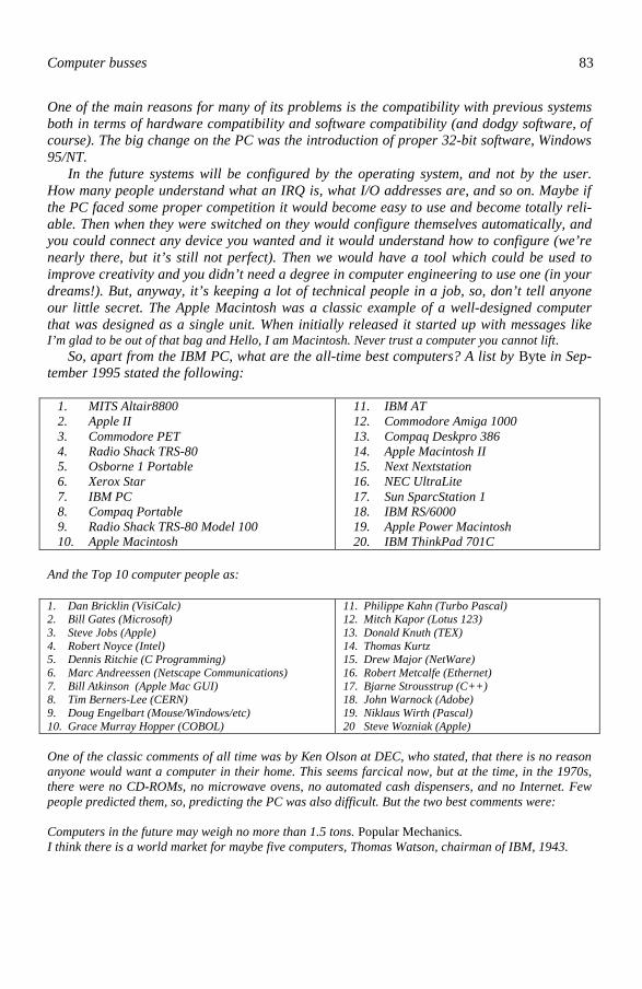
Computer busses 83
One of the main reasons for many of its problems is the compatibility with previous systems both in terms of hardware compatibility and software compatibility (and dodgy software, of course). The big change on the PC was the introduction of proper 32-bit software, Windows 95/NT. In the future systems will be configured by the operating system, and not by the user. How many people understand what an IRQ is, what I/O addresses are, and so on. Maybe if the PC faced some proper competition it would become easy to use and become totally reli-able. Then when they were switched on they would configure themselves automatically, and you could connect any device you wanted and it would understand how to configure (we’re nearly there, but it’s still not perfect). Then we would have a tool which could be used to improve creativity and you didn’t need a degree in computer engineering to use one (in your dreams!). But, anyway, it’s keeping a lot of technical people in a job, so, don’t tell anyone our little secret. The Apple Macintosh was a classic example of a well-designed computer that was designed as a single unit. When initially released it started up with messages like I’m glad to be out of that bag and Hello, I am Macintosh. Never trust a computer you cannot lift. So, apart from the IBM PC, what are the all-time best computers? A list by Byte in Sep-tember 1995 stated the following:
1. MITS Altair8800 2. Apple II 3. Commodore PET 4. Radio Shack TRS-80 5. Osborne 1 Portable 6. Xerox Star 7. IBM PC 8. Compaq Portable 9. Radio Shack TRS-80 Model 100 10. Apple Macintosh
11. IBM AT 12. Commodore Amiga 1000 13. Compaq Deskpro 386 14. Apple Macintosh II 15. Next Nextstation 16. NEC UltraLite 17. Sun SparcStation 1 18. IBM RS/6000 19. Apple Power Macintosh 20. IBM ThinkPad 701C
And the Top 10 computer people as: 1. Dan Bricklin (VisiCalc) 2. Bill Gates (Microsoft) 3. Steve Jobs (Apple) 4. Robert Noyce (Intel) 5. Dennis Ritchie (C Programming) 6. Marc Andreessen (Netscape Communications) 7. Bill Atkinson (Apple Mac GUI) 8. Tim Berners-Lee (CERN) 9. Doug Engelbart (Mouse/Windows/etc) 10. Grace Murray Hopper (COBOL)
11. Philippe Kahn (Turbo Pascal) 12. Mitch Kapor (Lotus 123) 13. Donald Knuth (TEX) 14. Thomas Kurtz 15. Drew Major (NetWare) 16. Robert Metcalfe (Ethernet) 17. Bjarne Strousstrup (C++) 18. John Warnock (Adobe) 19. Niklaus Wirth (Pascal) 20 Steve Wozniak (Apple)
One of the classic comments of all time was by Ken Olson at DEC, who stated, that there is no reason anyone would want a computer in their home. This seems farcical now, but at the time, in the 1970s, there were no CD-ROMs, no microwave ovens, no automated cash dispensers, and no Internet. Few people predicted them, so, predicting the PC was also difficult. But the two best comments were: Computers in the future may weigh no more than 1.5 tons. Popular Mechanics. I think there is a world market for maybe five computers, Thomas Watson, chairman of IBM, 1943.

Interfacing Standards
3.1 Introduction
The type of interface card used greatly affects the performance of a PC system. Early models of PCs relied on expansion options to improve their specification. These expansion options were cards that plugged into an expansion bus. Eight slots were usually available and these added memory, video, fixed and floppy disk controllers, printer output, modem ports, serial communications and so on. There are eight main types of interface busses available for the PC. The number of data bits they handle at a time determines their classification. They are: • PC (8-bit) ISA (16-bit) • EISA (32-bit) MCA (32-bit) • VL-Local Bus (32-bit) PCI bus (32/64-bit) • SCSI (16/32-bit) PCMCIA (16-bit)
3.2 PC bus
The PC bus uses the architecture of the Intel 8088 processor which has an external 8-bit data bus and 20-bit address bus. A PC bus connector has a 62-pin printed circuit card edge con-nector and a long narrow or half-length plug-in card. As it uses a 20-bit address bus, it can address a maximum of 1 MB of memory. The transfer rate is fixed at 4.772 727 MHz; thus, a maximum of 4 772 727 bytes can be transferred every second. Dividing a crystal oscillator frequency of 14.318 18 MHz by three derives this clock speed. Figure 3.1 shows a PC card. Figure 3.2 defines the signal connections. The direction of the signal is taken as input if a signal comes from the ISA bus controller. An output comes from the slave device and in-put/output identifies that the signal can originate from either the ISA controller or the slave device. The following gives the 8-bit PC bus connections: SA0-SA19 Address bus (input/output). The lower 20 bits of the system address bus.
D0-D7 Data bus (input/output). The eight data bits that allow a transfer between the busmaster and the slave.
AEN Address enable (output). The address enable allows for an expansion bus board to disable its local I/O address decode logic. It is active high. When active, ad-dress enable indicates that either DMA or refresh are in control of the busses.
3

86 Computer busses
CL340XYZ11
CL340
XYZ11CL340
CS220
MS
1432
Figure 3.1 PC card
CLK Clock (output). The bus CLK is set to 4.772 727 MHz (for PC bus and 8.33 MHz for ISA bus) and provides synchronisation of the data transmission (it is derived from the OSC clock).
ALE Address latch (output). The bus address latch indicates to the expansion bus that the address bus and bus cycle control signals are valid. It thus indicates the be-ginning of a bus cycle on the expansion bus.
IOR I/O read (input/output). I/O read command signal indicates that an I/O read cycle is in progress.
IOW I/O write (input/output). I/O write command signal indicates that an I/O write bus cycle is in progress.
SMEMR System memory read (output). System memory read signal indicates a memory read bus cycle for the 20-bit address bus range (0h to FFFFFh).
SMEMW System memory write (output). System memory write signal indicates a mem-ory read bus cycle from the 20-bit address bus range (0h to FFFFFh).
IO CH RDY Bus ready (input). The bus ready signal allows a slave to lengthen the amount of time required for a bus cycle.
B1
B2
B3
B4
B5
B6
B7
B8
B9
B10
B11
B12
B13
B14
B15
B16
B17
B18
B19
B20
B21
B22
B23
B24
B25
B26
B27
B28
B29
B30
B31
A1
A2
A3
A4
A5
A6
A7
A8
A9
A10
A11
A12
A13
A14
A15
A16
A17
A18
A19
A20
A21
A22
A23
A24
A25
A26
A27
A28
A29
A30
GN
D
RE
SE
T D
RV
+5V
IRQ
2
-5V
DR
Q2
-12
V
0WS
+12
V
GN
D
SM
EM
W
SM
EM
RIO
W
IOR
DA
CK
3
DR
Q3
DA
CK
1
DR
Q1
RE
FC
LK
IRQ
7
IRQ
6
IRQ
5
IRQ
4
IRQ
3
DA
CK
2
T/C
ALE +5V
OS
C
GN
D
I/O C
H C
HK
SD
7
SD
6
SD
5
SD
4
SD
3
SD
2
SD
1
SD
0I/O
CH
RD
Y
AE
N
SA
19
SA
18
SA
17
SA
16
SA
15
SA
14
SA
13
SA
12
SA
11
SA
10
SA
9
SA
8
SA
7
SA
6
SA
5
SA
4
SA
3
SA
2
SA
1
SA
0A
31
Figure 3.2 PC card connections
Interfacing standards 87
0WS Zero wait states (input). The zero wait states (or no wait state) allows a slave to shorten the amount of time required for a bus cycle.
DRQ1-DRQ3 DMA request (input). The DMA request indicates that a slave device is request-ing a DMA transfer.
DACK1-DACK3 DMA acknowledge (output). The DMA acknowledge indicates to the request-ing slave that the DMA is handling its request.
T/C Terminal count (input). The terminal count indicates that the DMA transfer has been successful and all the bytes have been transferred.
REF Refresh (output). The refresh signal is used to inform a memory board that it should perform a refresh cycle.
IRQ2-IRQ7 Interrupt request. The interrupt request signals indicate that the slave device is requesting service by the processor.
RESET DRV Reset drive (output). The reset drive resets and plug-in boards connected to the ISA bus.
OSC Crystal oscillator (output). The crystal oscillator signal is 14.318 18 MHz signal provided for use by expansion boards. This clock speed is three times the CLK speed.
CHK CH IO I/O check (input). The I/O check signal indicates that a memory slave has de-tected a parity error.
±5V, ±12V and GND Power (output).
3.3 ISA bus
IBM developed the ISA (Industry Standard Architecture) for their 80286-based AT (Ad-vanced Technology) computer. It had the advantage of being able to deal with 16 bits of data at a time. An extra edge connector gives compatibility with the PC bus. This gives an extra 8 data bits and 4 address lines. Thus, the ISA bus has a 16-bit data and a 24-bit address bus. This gives a maximum of 16 MB of addressable memory and like the PC bus it uses a fixed clock rate of 8 MHz. The maximum data rate is thus 2 bytes (16 bits) per clock cycle, giving a maximum throughput of 16 MB/sec. In machines that run faster than 8 MHz the ISA bus runs slower than the rest of the computer. A great advantage of PC bus cards is that they can be plugged into an ISA bus connector. ISA cards are very popular as they give good performance for most interface applications. The components used are extremely cheap and it is a well-proven reliable technology. Typi-cal applications include serial and parallel communications, networking cards and sound cards. Figure 3.3 illustrates an ISA card and Figure 3.4 gives the pin connections for the bus. It can be seen that there are four main sets of connections, the A, B, C and D sections (Figure 3.4). The standard PC bus connection contains the A and B sections. The A section includes the address lines A0–A19 and 8 data lines, D0–D7. The B section contains interrupt lines, IRQ0–IRQ7, power supplies and various other control signals. The extra ISA lines are added with the C and D section; these include the address lines, A17–A23, data lines D8–D15 and interrupt lines IRQ10–IRQ14.

88 Computer busses
CL340XYZ11
CL340
XYZ11CL340
CS220
MS
1432
ISA extension PC bus connector
Figure 3.3 ISA card
B1
B2
B3
B4
B5
B6
B7
B8
B9
B10
B11
B12
B13
B14
B15
B16
B17
B18
B19
B20
B21
B22
B23
B24
B25
B26
B27
B28
B29
B30
B31
D1
D2
D3
D4
D5
D6
D7
D8
D9
D10
D11
D12
D13
D14
D15
D16
D17
D18
A1
A2
A3
A4
A5
A6
A7
A8
A9
A10
A11
A12
A13
A14
A15
A16
A17
A18
A19
A20
A21
A22
A23
A24
A25
A26
A27
A28
A29
A30
A31
C1
C2
C3
C4
C5
C6
C7 C
8
C9
C10
C11
C12
C13
C14
C15
C16
C17
C18
GN
D
RE
SE
T D
RV +5
V
IRQ
2
-5V
DR
Q2
-12
V0W
S
+12
V
GN
D
SM
EM
W
SM
EM
RIO
W
IOR
DA
CK
3
DR
Q3
DA
CK
1
DR
Q1
RE
FC
LK
IRQ
7
IRQ
6
IRQ
5
IRQ
4
IRQ
3
DA
CK
2
T/C
BA
LE+5
V
OS
C
GN
D
ME
M C
S16
I/O C
S16
IRQ
10
IRQ
11
IRQ
12
IRQ
13
IRQ
14
DA
CK
0
DR
Q0
DA
CK
5
DR
Q5
DA
CK
6
DA
CK
6
DA
CK
7
DR
Q7
+5V
MA
STE
R
GN
D
I/O C
H C
HK
SD
7
SD
6
SD
5
SD
4
SD
3
SD
2
SD
1
SD
0I/O
CH
RD
Y
AE
N
SA
19
SA
18
SA
17
SA
16
SA
15
SA
14
SA
13
SA
12
SA
11
SA
10
SA
9
SA
8
SA
7
SA
6
SA
5
SA
4
SA
3
SA
2
SA
1
SA
0
SB
HE
SA
23
SA
22
SA
21
SA
20
SA
19
SA
18
SA
17M
EM
R
ME
MW
SD
8
SD
9
SD
10
SD
11
SD
12
SD
13
SD
14
SD
15
Figure 3.4 ISA bus connections
The Industry Standard Architecture (ISA) bus uses a 16-bit data bus (D0-D15) a 24-bit
address bus (A0–A24) and the CLK signal is set to 8.33 MHz. The SMEMR and SMEMW lines are used to transfer data for the lowest 1 MB (0h to FFFFFh) of memory (where the S prefix can be interpreted as small memory model) and the signals MEMR and MEMW are used to transfer data between 1 MB (FFFFFh) and 16 MB (FFFFFFh). For example if reading from
the address is 001000h then the SMEMR the line is made active low, while if the address 1F0000h then the MEMR line is made active. For a 16-bit transfer the M16 and IO16 lines are made active. The extra 16-bit ISA bus connections are: A17-A23 Address bus (input/output). The upper 7 bits of the address of the
system address bus.
SBHE System byte high enable (output). The system byte high enable indicates that data is expected on the upper 8 bits of the data bus (D8–D15).
D8-D15 Data bus (input/output). The upper 8 bits of the data bus provides for the second half of the 16-bit data bus.

Interfacing standards 89
MEMR Memory read (input/output). The memory read command indicates a memory read when the memory address is in the range 100000h –FFFFFFh (16 MB of memory).
MEMW Memory write (input/output). The memory write command indi-cates a memory write when the memory address is in the range 100000h – FFFFFFh (16 MB of memory).
M16 16-bit memory slave. Indicates that the addressed slave is a 16-bit memory slave.
IO16 16-bit I/O slave (input/output). Indicates that the addressed slave is a 16-bit I/O slave.
DRQ0, DRQ5-DRQ7 DMA request lines (input). Extra DMA request lines that indicate that a slave device is requesting a DMA transfer.
DACK0, DACK5-DACK7 DMA acknowledge lines (output). Extra DMA acknowledge lines that indicate to the requesting slave that the DMA is handling its re-quest.
MASTER Bus ready (input). This allows another processor to take control of the system address, data and control lines.
IRQ9-IRQ12, IRQ14, IRQ15 Interrupt requests (input). Additional interrupt request signals that indicate that the slave device is requesting service by the processor. Note that the IRQ13 line is normally used by the hard disk and in-cluded in the IDE bus.
3.3.1 Handshaking lines
Figure 3.5 shows a typical connection to the ISA bus. The ALE (or sometimes known as BALE) controls the address latch and, when active low, it latches the address lines A2–A19 to the ISA bus. The address is latched when ALE goes from a high to a low. The Pentium’s data bus is 64 bits wide, whereas the ISA expansion bus is 16-bits wide. It is the bus controller’s function to steer data between the processor and the slave device for either 8-bit or 16-bit communications. For this purpose the bus controller monitors BE0 –BE3 , R/W , M16 and IO16 to determine the movement of data. When the processor outputs a valid address it sets address lines (AD2–AD31), the byte enables ( BE0 – BE3 ) and sets ADS active. The bus controller then picks up this address and uses it to generate the system address lines, SA0–SA19 (which are just a copy of the lines A2–A19. The bus controller then uses the byte enable lines to generate the address bits SA0 and SA1. The EADS signal returns an active low signal to the processor if the external bus control-ler has sent a valid address on address pins A2–A21. It can be seen from Figure 3.6 that the BE0 line accesses the addresses ending with 0h, 4h, 8h and Ch, the BE1 line accesses addresses ending with 1h, 5h, 9h and Dh, the BE2 line accesses addresses ending with 02, 5h, Ah and Eh, and so on. Thus if the BE0 line is asserted and the SBHE line is high then a single byte is accessed through the D0–D7. If a word is to be accessed then SBHE is low and D0–D15 contains the data.

90 Computer busses
Buscontroller
Addresslatch
Memory
ALE
A0
A1
SBHE
M16
IO16
ISAbus
EADS
A2-A19A2-A31
BE0-BE3
Processor
Datalatch
D0-D31D0-D15
Figure 3.5 ISA bus connections
0000h 0001h 0002h 0003h 0004h 0005h 0006h 0007h 0008h 0009h 000Ah
BE0 BE1 BE2 BE3 BE0 BE1 BE2 BE3 BE0 BE1 BE2
0 1 2 3
4 5 6 7
8 9 A B
C D E F
BE0 BE1 BE2 BE3 D0–D7
D8–D15 D16–D23
D24–D31
Figure 3.6 Address decoding
Table 3.1 shows three examples of handshaking lines. The first is an example of a byte trans-fer with an 8-bit slave at an even address. The second example gives a byte transfer for an 8-bit slave at an odd address. Finally, the table shows a 2-byte transfer with a 16-bit slave at an even address.
Table 3.1 Example handshaking lines
BE0 BE1 BE2 BE3 IO16 M16 SBHE SA0 SA1 Data 0 1 1 1 1 1 1 0 0 SD0–SD7 1 0 1 1 1 1 0 1 0 SD8–SD15 0 0 1 1 0 1 0 0 0 SD0–SD15
If 32-bit data is to be accessed then BE0–BE3 will each be 0000 which makes 4 bytes active. The bus controller will then cycle through SA0, SA1 = 00 to SA0, SA1 = 11. Each time the 8-bit data is placed into a copy buffer which is then passed to the processor as 32 bits.

Interfacing standards 91
3.3.2 82344 IC
Much of the electronics in a PC has been integrated onto single ICs. The 82344 IC is one that interfaces directly to the ISA bus. Figure 3.7 shows its pin connections.
CL
KB
AL
EA
EN
-IO
R-
IOW
-R
EF
RS
T D
RV
- SM
EM
R-
SEM
W- S
BH
E-
DA
CK
0-
DA
CK
1-
DA
CK
2-
DA
CK
3-
DA
CK
5-
DA
CK
6-
DA
CK
7D
RQ
0D
RQ
1D
RQ
2D
RQ
3D
RQ
5D
RQ
6D
RQ
7T
/C -M
AS
TE
R-
ME
M C
S16
-IO
CS1
6-
IOC
HK
IOC
HR
DY
-0W
SIR
Q1
IRQ
3IR
Q4
IRQ
5IR
Q6
IRQ
7IR
Q9
IRQ
10IR
Q11
IRQ
12IR
Q13
IRQ
14IR
Q15
SA
0S
A1
SA
2S
A3
SA
4S
A5
SA
6S
A7
SA
8S
A9
SA
10S
A11
SA
12S
A13
SA
14S
A15
SA
16S
A17
SA
18S
A19
SA
17S
A18
SA
19S
A20
SA
21S
A22
SA
23
A2
A3
A4
A5
A6
A7
A8
A9
A10
A11
A12
A13
A14
A15
A16
A17
A18
A19
A20
A21
A22
A23
A24
A25
-A
DS
XTALIN
XTALOU
TPS
VBAT
SPK
RX
D0
XD
1X
D2
XD
3X
D4
XD
5X
D6
XD
7-
XR
EA
D-
SD
SWA
PS
DH
L-
LA
TLO
- LA
TH
IPC
KP
OW
ER
GO
OD
-R
OM
B-
HID
RIV
E-
386D
X-
CS
8042
INTR
NM
IH
LD
A-
BE
0-
BE
1- B
E2
- BE
03-C
HR
EAD
Y- C
HS
0-
CH
S1
CH
M-
BL
KA
20D
MA
HR
QD
MA
HD
LA-
BR
DR
AM
OU
T1
- TR
I
8234
4IS
AC
ontr
olle
r
148
6 128
134
132
146
122
129
127
14 29 142
2 136
34 37 39 32 144
124
138
36 38 41 4 42 13 15 121
126
125
109
159
157
155
153
151
123
17 21 23 110
27 25 12 11 8 7 5 3 1 158
156
154
152
149
147
145
143
141
137
135
133
131
31 28 26 24 22 18 16
69 67 66 65 64 63 62 61 58 57 56 55 54 53 52 51 50 49 48 47 46 45 44 43 83 118
119
117
116
107
99 98 97 96 95 94 92 91 103
101
102
104
105
111
115
112
113
73 108
75 76 74 72 71 70 69 85 77 78 82 87 89 88 84 90 114
26
Figure 3.7 82344 IC connections
3.4 Other legacy busses
Two other busses which were used in the past are:
• MCA. IBM developed the Microchannel Interface Architecture (MCA) bus for their PS/2 computers. This bus is completely incompatible with ISA bus. It can operate as a 16-bit or 32-bit data bus. The main technical difference between the MCA and PC/ISA (and EISA) is that the MCA is an asynchronous bus whereas PC/ISA/EISA use a syn-chronous bus. An synchronous bus works at a fixed clock rate whereas an asynchronous bus data transfer is not dependent on a fixed clock. Asynchronous buses take their tim-ings from the devices involved in the data transfer (that is, the processor or system clock). The original MCA specification resulted in a maximum transfer rate of 160 MB/sec. Very few manufacturers have adopted MCA technology and it is mainly found in IBM PS/2 computers.
• EISA. Several manufacturers developed the EISA (Extended Industry Standard Archi-tecture) bus in direct competition to the MCA bus. It provides compatibility with PC/ISA but not MCA. The EISA connector looks like an ISA connector. It is possible to plug an ISA card into an EISA connector, but a special key allows the EISA card to be inserted

92 Computer busses
deeper into the EISA bus connector. It then makes connections with a 32-bit data and address bus. An EISA card has twice the number of connections over an ISA card and there are extra slots that allow it to be inserted deeper into the connector. The ISA card only connects with the upper connectors because it has only a single key slot. EISA uses a synchronous transfer at a clock speed of 8 MHz. It has a full 32-bit data and address bus and can address up to 4 GB of memory. In theory the maximum transfer rate is 4 bytes for every clock cycle. As the clock runs at 8 MHz, the maximum data rate is 32 MB/s.
3.5 Comparison of different types
Data throughput depends on the number of bytes being communicated for each transfer and the speed of the transfer. With the PC, ISA and EISA buses this transfer rate is fixed at 8 MHz, whereas the PCI and VL local buses use the system clock. For many applications the ISA bus offers the best technology as it has been around for a long time, it gives a good data throughput and it is relatively cheap and reliable. It has a 16-bit data bus and can thus trans-fer data at a maximum rate of 16 MB/s. The EISA bus can transfer four bytes for each clock cycle, thus if four bytes are transferred for each clock cycle, it will be twice as fast as ISA. The maximum data rates for the different interface cards are:
PC 8 MB/s ISA 16 MB/s EISA 32 MB/s VL-Local bus 132 MB/s (33 MHz system clock using 32-bit transfers) PCI 264 MB/s (33 MHz system clock using 64-bit transfers) MCA 20 MB/s (160 MB/s burst)
The type of interface technology used depends on the data throughput. Table 3.2 shows some typical transfer data rates. The heaviest usage on the system are microprocessor to memory and graphics adaptor transfers. These data rates depend on the application and the operating system used. Graphical user interface (GUI) programs have much greater data throughput than programs running in text mode. Notice that a high specification sound card with re-cording standard quality (16-bit samples at 44.1 kHz sampling rate) only requires a transfer rate of 172 kB/s. The transfer rate for audio is:
kB/s 172.261024
400 166
B/s 400 176
B/s 2)2100 44(
(B/s) sampleper bytes ofNumber secondper samples ofNumber fi)-(hi rateTransfer
==
=××=
×=
A standard Ethernet local area network card transfers at data rates of up 10 Mbps (about 1 MB/s), although new fast Ethernet cards can transfer at data rates of up to 100 Mbps (about 10 MB/s). These transfers thus require local bus type interfaces.

Interfacing standards 93
Table 3.2 Example transfer rates
Device Transfer rate Application Hard disk 4 MB/s Typical transfer Sound card 88 KB/s 16-bit, 44.1 kHz sampling LAN 1 MB/s 10 Mbps Ethernet RAM 66 MB/s Microprocessor to RAM Serial Communications 1 KB/s 9600 bps Super VGA 15 MB/s 1024×768 pixels with 256 colours
For a graphics adaptor with a screen resolution of 1024×640, 64k colours (16-bit colour) which is updated 20 times per second (20 Hz), the maximum transfer rate will be:
MB/s 246.210241024
400 214 26
B/s 400 214 268
200 715 209
b/s 200 715 209
b/s 2016)6401024(
(b/s) updatesscreen of No.pixelper bits of No.screenper pixels of No.(max) rateTransfer
=×
=
==
=×××=
××=
The PCI Local bus has become a standard on most new PC systems and has replaced the VL-local bus for graphics adaptors. It has the advantage over the VL-local bus in that it can transfer at much higher rates. Unfortunately, most available software packages cannot use the full power of the PCI bus because they do not use the full 64-bit data bus. PCI and VL-local bus are discussed in the next chapter.
3.6 Exercises
3.6.1 How many bits are transferred in a single clock operation with the PC bus: (a) 1 (b) 8 (c) 16 (d) 32 3.6.2 What is the standard clock frequency which is used in ISA transfers: (a) 4.77 MHz (b) 8 MHz (c) 10 MHz (d) 16 MHz 3.6.3 What is the maximum transfer rate for the ISA bus: (a) 8 MB/s (b) 16 MB/s (c) 32 MB/s (d) 64 MB/s 3.6.4 What is the maximum transfer rate for the EISA bus: (a) 8 MB/s (b) 16 MB/s

94 Computer busses
(c) 32 MB/s (d) 64 MB/s 3.6.5 What is the main disadvantage of PC, ISA and EISA busses: (a) They are incompatible with each other. (b) They use a fixed clock frequency. (c) They are not supported in PC systems. (d) They are expensive to implement. 3.6.6 What is the maximum transfer rate (in B/s) for a 10 Mbps Ethernet adaptor: (a) 1 MB/s (b) 1.221 MB/s (c) 10 MB/s (d) 100 MB/s 3.6.7 Prove, apart from the MCA bus, the transfer rates given in Section 3.5. 3.6.8 If an audio card is using 16-bit sampling at a rate of 44.1kHz. Prove that the trans-
fer rate for stereo sound will be 176.4 KB/sec. Show, also that this is equivalent to 1.411 Mbps (note that this is approximately the standard rate for CD-ROMs). Can this rate be transferred using the ISA bus? Using this transfer rate, determine the maximum transfer speed of a ×32 CD-ROM drive.
3.6.9 Determine amount of data for a single screen that required to be transferred for the
following screen resolutions:
(a) 800×600, 65 536 colours (960 000 B/s). (b) 800×600, 16 777 216 colours (1 440 000 B/s). (c) 1024×768, 65 536 colours (1 572 864 B/s). Determine the maximum number of screen updates that is required for a 32-bit PCI bus for each of the above.
3.6.10 Identify the main ISA signal lines and how they are used to transfer data. Answer clearly the following:
(a) The main differences between a PC card and an ISA card. (b) How the byte enable lines are used. (c) How is a read or write transfer identified? (d) How is a memory read/write or isolated memory read/write transfer identi-
fied? (e) The interrupt lines which are available on a PC card and an ISA card.
Typically what devices could be supported by a PC card (that is, what devices use
the interrupts that a PC card can support). How does this related to the original specification of the PC?

Interfacing standards 95
3.7 Summary of interface bus types
Devices connect to the microprocessor using a computer bus. The specification of this bus defines the transfer speed between the microprocessor and the connected device. Peripherals can connect to the computer using either an internal or an external interface. Table 3.3 and Table 3.4 give some examples of typical PC interfaces.
Table 3.3 Internal PC busses
Bus Description Typical devices connected
ISA The ISA (International Standards Architecture) bus uses an inter-face card which has two edge connectors (as one of the connec-tors was used on the original PC bus). Typical ISA connections are network interface adaptors, video camera interfaces and sound cards. It can transfer up to 16 bits at a time, and uses a fixed transfer rate of 8 MHz (8 000 000 transfers every second). Max: 16 MB/s.
Network adaptor Video camera adaptor Sound card
PCI The PCI (Peripheral Component Interconnection) bus is used connect internal devices in the PC. Typically, modern PCs have at least four PCI adaptors, which are used to connect to network interface cards, graphics adaptors and sound cards. It can transfer up to 32 bits at a time. Max: 132 MB/s (more typically, 66 MB/s).
Network adaptor Video camera adaptor Sound card
AGP The AGP (Accelerated Graphics Port) bus is used solely to con-nect to video cards. It uses a special connector, but builds on the standard PCI bus. It is optimised so that it uses the main memory of the computer, and does not depend on memory on the graphics card. Max: 500 MB/s.
Graphics adaptor
IDE The Integrated Drive Electronics (IDE) bus is used solely to con-nect to either hard disk drives, or CD-ROM drives. There are two IDE connections: IDE0 and IDE1. Up to two devices can connect to each IDE connector, thus up to four disk drives can connect to the IDE bus. Max: 16.6 MB/s (IDE, Mode 4).
Hard disk drive CD-ROM drive
PCMCIA The Personal Computer Memory Card International Association (PCMCIA) interface allows small thin cards to be plugged into laptop, notebook or palmtop computers. It was originally de-signed for memory cards (Version 1.0) but has since been adopted for many other types of adapters (Version 2.0), such as fax/modems, sound-cards, local area network cards, CD-ROM controllers, digital I/O cards, and so on. Most PCMCIA cards comply with either PCMCIA Type II or Type III. Type I cards are 3.3 mm thick, Type II take cards up to 5 mm thick, Type III allows cards up to 10.5 mm thick. A new standard, Type IV, takes cards which are greater than 10.5 mm. Type II interfaces can accept Type I cards, Type III accept Types I and II and Type IV interfaces accept Types I, II and III. It uses a 16-bit data trans-fer.
Network adaptor Modem adaptor Sound card CD-ROM drive Memory upgrade Hard disk drive
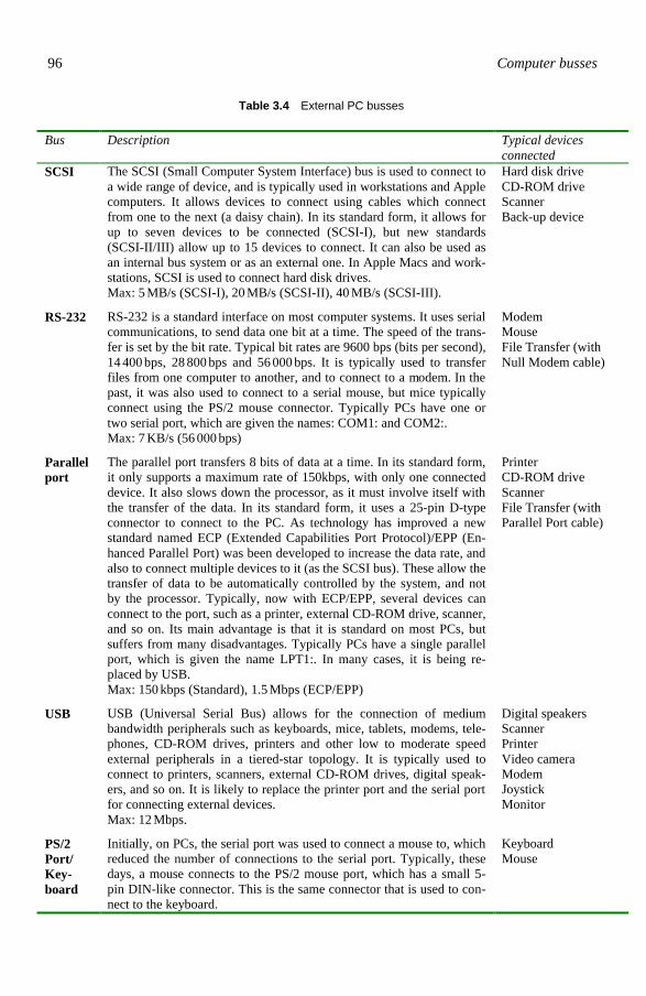
96 Computer busses
Table 3.4 External PC busses
Bus Description Typical devices connected
SCSI The SCSI (Small Computer System Interface) bus is used to connect to a wide range of device, and is typically used in workstations and Apple computers. It allows devices to connect using cables which connect from one to the next (a daisy chain). In its standard form, it allows for up to seven devices to be connected (SCSI-I), but new standards (SCSI-II/III) allow up to 15 devices to connect. It can also be used as an internal bus system or as an external one. In Apple Macs and work-stations, SCSI is used to connect hard disk drives. Max: 5 MB/s (SCSI-I), 20 MB/s (SCSI-II), 40 MB/s (SCSI-III).
Hard disk drive CD-ROM drive Scanner Back-up device
RS-232 RS-232 is a standard interface on most computer systems. It uses serial communications, to send data one bit at a time. The speed of the trans-fer is set by the bit rate. Typical bit rates are 9600 bps (bits per second), 14 400 bps, 28 800 bps and 56 000 bps. It is typically used to transfer files from one computer to another, and to connect to a modem. In the past, it was also used to connect to a serial mouse, but mice typically connect using the PS/2 mouse connector. Typically PCs have one or two serial port, which are given the names: COM1: and COM2:. Max: 7 KB/s (56 000 bps)
Modem Mouse File Transfer (with Null Modem cable)
Parallel port
The parallel port transfers 8 bits of data at a time. In its standard form, it only supports a maximum rate of 150kbps, with only one connected device. It also slows down the processor, as it must involve itself with the transfer of the data. In its standard form, it uses a 25-pin D-type connector to connect to the PC. As technology has improved a new standard named ECP (Extended Capabilities Port Protocol)/EPP (En-hanced Parallel Port) was been developed to increase the data rate, and also to connect multiple devices to it (as the SCSI bus). These allow the transfer of data to be automatically controlled by the system, and not by the processor. Typically, now with ECP/EPP, several devices can connect to the port, such as a printer, external CD-ROM drive, scanner, and so on. Its main advantage is that it is standard on most PCs, but suffers from many disadvantages. Typically PCs have a single parallel port, which is given the name LPT1:. In many cases, it is being re-placed by USB. Max: 150 kbps (Standard), 1.5 Mbps (ECP/EPP)
Printer CD-ROM drive Scanner File Transfer (with Parallel Port cable)
USB USB (Universal Serial Bus) allows for the connection of medium bandwidth peripherals such as keyboards, mice, tablets, modems, tele-phones, CD-ROM drives, printers and other low to moderate speed external peripherals in a tiered-star topology. It is typically used to connect to printers, scanners, external CD-ROM drives, digital speak-ers, and so on. It is likely to replace the printer port and the serial port for connecting external devices. Max: 12 Mbps.
Digital speakers Scanner Printer Video camera Modem Joystick Monitor
PS/2 Port/ Key-board
Initially, on PCs, the serial port was used to connect a mouse to, which reduced the number of connections to the serial port. Typically, these days, a mouse connects to the PS/2 mouse port, which has a small 5-pin DIN-like connector. This is the same connector that is used to con-nect to the keyboard.
Keyboard Mouse

Interfacing standards 97
3.8 The fall of the MCA bus
The leading computer companies of 1987 were Intel, IBM, Compaq, and Microsoft, but a special mention must go to Apple, Commodore and Sun Microsystems, who fought bravely against the growing IBM PC market. With the release of the IBM AT and now the PS/2, IBM had presented Intel with a large market for their 80286 design, but it was Compaq who increased it even more with the release of the DeskPro 386. The new Intel processors were now so successful that Intel had little to do, but try to keep up with demand, and try to stop cloners from copying their designs. They could now consolidate on their success with other support devices, such as the 80387-math coprocessor. By the end of the year, their only real mass-market competitor was Motorola, who released their excellent Motorola 68030 micro-processor, which would become the foundation of many Apple Mac computers. Within a few years, Motorola would become extremely reliant on the Apple Mac, while Intel held onto the PC market. At IBM, things were hectic. They were phasing out their IBM PC range, and introduced their new computer range, the PS/2. IBM realised that the open architecture of the IBM PC held little long term advantages for them, as clone manufacturers could always sell com-puters at much less cost than themselves. IBM had large development teams, sales staff, dis-tribution centres, training centres, back up support, and so on. They thus need to make enough profit on each computer to support all these functions. The PS/2 was their attempt at trying to close the open system, and make one that required to be licensed through them-selves. It was also an attempt at trying to reduce some of the problems that were caused with the limited technology of the IBM PC. One of the main problems was the PC bus, which allowed users to easily add peripherals to the computer, by plugging them into the system with a standard card which had a standard edge connector. Initially this used an 8-bit data bus, and operated at 8 MHz, which gave a data throughput of 8 MB/s (as one byte is 8 bits). This was upgraded on the AT computer with the AT bus, which used a 16-bit data bus, giv-ing a data throughput of 16 MB/s. The great advantage of the AT bus, was that it was still compatible with the PC bus, where PC bus cards could still be slotted into AT bus connectors (soon to be renamed the ISA, or Industry Standard Bus). The AT bus was fine for slow devices, such as printer, modems, and so on. However, for colour graphics it was far to slow. For example, a colour monitor with a resolution of 640×480, with 256 colours (8 bits per colour), and a screen refresh of 25 Hz, requires a data throughput of 7 680 000 B/s (640×480×1×25 B/s). IBM’s concept was to use a bus, which, intentionally, had a different connector to the PC and the AT bus, which did not use a fixed clock rate, and could thus operate at the speed of the processor, which was now moving above 20 MHz. The MCA (Micro Channel Architec-ture) bus also used a 32-bit data bus, which allowed data throughputs of 100 MB/s. The PS/2 was an excellent concept, and was boosted by an extensive advertising cam-paign that boosted performance improvement over previous systems. It was the right move, and the system looked well, with 3.5-inch disk drives, and a rugged gray plastic case. Com-puters had never look so professional. For many businesses, they were heaven sent. How-ever, the fly-in-the-ointment for IBM was Compaq, who had previously released their Desk-Pro 386. The big problem with the PS/2 range was that the lower-end PCs were based on the 8086 and the 80286, and against the 80386-based Compaq they seem slow. The initial range was:
• Model 30, which used the, at the time, relatively slow, 8 MHz 8086. IBM also intro-

98 Computer busses
duced the Model 25, also with an 8 MHz Intel 8086, which had no hard drive, and a re-duced keyboard for $1350.
• Model 50 and 60, which used a 10 MHz 80286 with MCA. • Model 80, which used a 20 MHz 80386 with MCA. In 1988, the battle lines had been drawn the year before. IBM was trying to pull the market towards their architecture. The strength, of this was highlighted by John Akers, the then IBM Chairman: We’re trying to change the habits of an awful lot of people. That won’t happen overnight, but it will bloody well happen. IBM thought they would win the battle, and the older IBM PC architecture would die off. Several companies went with IBM, including Tandy (Tandy 5000MC), Dell and Olivetti. But the first signs of problems for IBM came when 61 companies developed the 32-bit version of the ISA bus, the EISA (Extended Industry Standard Architecture). This allowed 32 bits to be transferred at a time. Unfortunately, it was still based on an 8 MHz clocking rate, which gave it a data throughput of 32 MB/s. It was supported by the leading computer companies, such as Compaq Computer, AST, Epson, Hewlett-Packard, NEC Technologies, Olivetti, Tandy, Wyse, Zenith, and Microsoft. Along with this, Compaq Computer and eight other companies started developing the ISA standard to improve the AT-bus. Rod Canion, the Compaq Com-puter and CEO, showed his company’s resistance to the MCA bus: If people are going to buy Micro Channel, they’re going to buy it from IBM. The market would eventually reject the MCA bus, mainly because of the weight of the new x86, 80386 computers on the market. It would take a company such as Intel to develop a totally new bus system: the PCI bus.
3.9 Notes from the author
Oh boy, is it confusing! There are so many different busses used in systems, especially in PCs. There are three main reasons for the number of busses: legacy, compatibility and effi-ciency. With legacy, busses exist because they have existed in the past, and are required to be supported for the time being. With compatibility, busses allow the segmentation of a sys-tem and provide, most of the time, a standard interface that allows an orderly flow of data and allows manufactures to interconnect their equipment. If allowed, many manufacturers would force users to use their own versions of busses, but the trend these days is to use inter-nationally defined busses. Efficient busses have been designed to take into account the type of data that is being transmitted. So, in the end, we win. Sometimes, though, the bus technology does always win, and manufacturers who try to develop systems on their own can often fail miserably. This has been shown with the MCA bus, which was an excellent step in bus technology, and made up for the mistakes made in the original PC design. But, IBM tried to force the market, and failed. In these days, it is international standards that are important. Products to be accepted in the market or in the industry require an international standards body to standardise them, such as the IEEE, the ISO, ANSI and so on. Without them, very few companies will accept the product. A classic
Interfacing standards 99
case of an open standard winning against a closed system was Betamax video which was a closed standard produced by Sony, up against VHS which was an open standard. VHS was the inferior technology, but won because there were more companies willing to adopt it. The days of having a single computer bus for internal and external connections are a long way off (if ever), as there will always be some peripherals that need to transmit data in a certain way that differs from other peripheral. Also standard technology always tends to win over newer, faster technology. Few companies can now define new standards on their own. Before we start to look at the technology behind computer busses, here is my All-Time Best Busses (in order of their current and future usefulness).
TOP BUSSES OF ALL-TIME AWARD
1. PCI bus. An excellent internal bus that provides the backbone to most modern PCs. It has been a complete success, and provides for many modern enhancements, such as plug-and-play technology, steerable interrupts, and so on. In its acceptance speech for Best Bus of All-Time it would thank the VL-local bus for starting the trend toward local bus technology. The VL-local bus held-the-fort for a short time, and gave a short-term fix for high-speed graphics transfers, but Intel busily developed a proper bus which could support other high-speed devices. With local bus technology, low-speed devices were pushed away from the processor, and can only communicate with it over a bridge. A worthy champion that is the bedrock of modern computing. It even has a few trump cards yet to play (including increasing its transfer rate, integration with the AGP port, and increasing its data bus size).
2. SCSI bus. The most general-purpose of the external busses and in many respects as great as the PCI bus, but it looses out to the PCI bus in that it is not used in as many computers. It provides an easy method of connecting external devices in a daisy-chain connection. New standards for the SCSI bus support fast transfer rates (over 40 MB/s), and allow up to 15 internal or external devices to be connected.
3. USB. An external bus which shows great potential in the way that it integrates many of the low and medium bit rate devices onto a single bus system. New standards for USB are trying to also integrate high bit rate devices. It supports hot plug-and-play, which allows users to connect and disconnect peripherals from the bus, while the computer is still on.
4. AGP port. The PCI, SCSI and USB busses are a long-way out in front to the other busses, and the forth place in the table goes to AGP port which overcomes the last great problem area of the PC: the graphics adaptor. AGP provides for fast transfer rates using the PCI bus as a foundation, and allows the PC to use local memory for graphics transfers.
5. PCMCIA. A long way behind in fifth place comes the PCMCIA bus, which is an ex-ternal bus that provides for easy upgrades on notebook technology. It highlights how small and compact interface devices can be. Typical additions are modem and net-work adaptors. Its future will depend on how the USB bus is used in the future.
And let’s not forget the busses which have helped us to get to this point. We may call them legacy busses, but they have allowed us to get to where we are now, and still provide a useful function. Thus, the awards for the Most Helpful Busses of the Past (in order of their previous usefulness) are given next.

100 Computer busses
MOST HELPFUL BUSSES OF ALL-TIME 1. ISA bus. The ISA bus competed head-to-head with the MCA, and although it was
much slower, it triumphed, as it was compatible with the older PC bus. For many years its performance was acceptable (16MB/s), but the advent of the graphical user interface was the beginning of the end for it. It has sadly seen the number of PCI slots increasing while it has seen its own connections reduce from over five, to less than two.
2. RS-232 port. A classic bus, which is compatible (almost) with all the other RS-232 ports on every computer in the world. It provides a standard way to talk to devices, such as instruments, other computers, and modems.
3. IDE bus. A rather quiet and unassuming internal bus, which does its job of interfac-ing to disk drives well, without, these days, much troubles. It has reasonable perform-ance (over 14MB/s) and does not really have any intentions of ever becoming any-thing other than a disk interfacing bus. It, like Ethernet, has overcome early retire-ment by increasing its transfer rate, but still keeping compatibility with previous sys-tems. Its main competitor is SCSI, which is unlikely to ever to beat it for compatibility and cost, thus it is likely to stay around for much longer than some of its earlier PC partners. For systems which have less than four disk drives (in a combination of CD-ROM or hard disks) it is still the best choice, and is often integrated in the PC moth-erboard.
4. VL-Local bus. The bus that showed the way for local bus technology, especially the PCI bus. It always knew that it was a short-term fix, but it did its job effectively and quietly. Apart from the 80486, it was one of leading factors which increased the adop-tion of Microsoft Windows (as it allowed the fast transfer to graphical data).
5. Parallel port. Another classic bus which was created to purely interface to an exter-nal printer, but has now been developed to support a multi-attachment busses with reasonable transfer rates (over 150kB/s).
Let’s not forget about the great-grandfather of all the PC busses: the PC bus. It is now en-joying a well-earned retirement (but can be pulled back from retirement at any time). It is the bus that has launched a million computers. Finally, the relegation zone for computer busses (in order of the problems that they have caused or for their lack of adoption).
RELEGATION ZONE FOR BUSSES
1. ISA bus. Like the 8088 processor and DOS, it has a Dr Jekyll and Mr Hyde appear-ance, and is both the top computer bus of all-time, and worst bus of all-time. It is the bus, which, in the past, has provided the foundation for upgrading the PC, and has gently handed over its mantel to the PCI bus. But, it has caused lots of problems as it quickly fossilized the connection between the processor and the peripherals. Its major problems were it fixed rate transfer rate, the way that it handled interrupts, its lack of address lines (only up to 24), its lack of data lines (only up to 16), and the way that fast, medium and slow devices all connected to the same bus (thus allowing slow de-vices to ‘hog’ the bus). It started to show its age when 32-bit processors appeared and as the motherboard speeds increased. The beginning of its end was the introduc-tion of Microsoft Windows 3, which started to properly use a graphical user interface. The VL-local bus quickly came in as a stand-in. From there on, local bus technology

Interfacing standards 101
become the standard way to transfer large amounts of data. 2. MCA bus. IBM tried to pull the standard for bus technology back to a closed system
with the MCA bus. It failed as it came up against the technologically inferior ISA, as the ISA bus was an open standard.
3. VME bus. Powerful, complex and very misunderstood. Avoid in the same way that you would avoid the plague. The designers decided to create a bus that had every-thing, all that’s lacking is kitchen sink.
4. RS-232 port. Another bus, along with the ISA bus, which manages to get into the Top 5 busses of all-time, and also into the relegation zone. It is an extremely useful bus, but suffers because of a lack of speed and its incompatibility (even although everyone is working to the same standard, the level of implementation of the standard varies).
5. Keyboard connection/serial port mouse connection. Two extremely limited connec-tors. The keyboard connector has virtually no intelligence built into it, and provides for limited sensing of the keyboard type, or extra functionality. Its only real advantage is that it looks so different from other connectors. Another advantage is that is has al-lowed the integration of the new PS/2-type mouse connector. Serial port mouse con-nections have always caused problems, mainly because the use up one of the serial port connection.
Well that’s the bus awards. As we still have half a page to complete, here’s the winners of the specialist technologies: • Local Area Networking bus award:
1. Ethernet (one horse race). Although ISDN deserves a mention. • Wide Area Networking bus award:
1. ATM. A proper networking technology that integrates real-time signals (such as speech) and non-real-time data (such as computer data) into a networking tech-nology.
2. Gigabit Ethernet. Uses standard Ethernet technology to gives an extremely fast transfer rate, but still suffers from the problems of the original Ethernet specifica-tion.
3. FDDI. A reliable ring-based networking technology that allows for the transmis-sion of data over a large geographical area.
• Instrumentation bus award: 1. RS-422. An excellent bus which allows multiple attachments to a single bus, and
up to 1Mbps. 2. IEEE-488. An easy-to-use, robust, widely used, standardised and easy-to-connect-
to bus, which is rather limited, but extremely useful. 3. CAN bus. An excellent multi-drop system, for closely connected devices, especially
in automobile applications. It overcomes some of the problems that Ethernet has, as devices are so closely connected.
• Interconnecting protocol award. 1. TCP/IP (one horse race).

PCI Bus
4.1 Introduction
The PC was conceived at a time when processor clock speeds were measured in several MHz. Initially this was set at 4.77 MHz, and then increased to 8 MHz. The PC and ISA bus-ses fossilised with these clock frequencies. In the first few years of its design, the mother-board ran at the same speed as the processor. Soon, with improvements in silicon design, the speed of the processor was increased to tens of megahertz. Soon the maximum limit of the motherboard was reached and the only way to break this limit was to double or treble the motherboard clock speed. This limit was set at 33 MHz or 50 MHz. Processor speed has since been risen to over 500 MHz. Local bus technology uses the speed of the motherboard, rather than a fixed rate. Most new PCs have a motherboard speed of 100 MHz, which is at least twice as fast as 50 MHz motherboards. The greatest need for greater data throughput is the video adaptor. A high-resolution video screen with high screen update rate can require burst rates of over 100 MB/s. For ex-ample a screen of 1024×640 with 16.7 million colours (24-bit colour) will require the follow-ing amount of memory for a single screen:
1.875MB10241024
080 966 1
B 080 966 1
B 36401024Memory
=×
==
=××=
If this screen is updated 10 times every second (10Hz) then the data throughput is :
MB/s 37.5
MB/s 20875.1 transferData
=×=
This transfer rate is far too fast for busses such as ISA and EISA, and the only solution is a fast 32-bit bus, transferring at a rate of at least 33 MHz. The maximum transfer rates for vari-ous local bus transfers are as follows: Data bus size Transfer clock (MHz) Data transfer rate (MB/s) 16 33 66 16 50 100 32 33 132 32 50 200 32 100 320 64 50 400
4

104 Computer busses
Intel have developed a standard interface, named the PCI (Peripheral Component Inter-connection) local bus, for the Pentium processor. This technology allows fast memory, disk and video access. A standard set of interface ICs known as the 82430 PCI chipset is available to interface to the bus. Figure 4.1 shows how the PCI bus integrates into the PC. The proces-sor runs at a multiple of the motherboard clock speed, and is closely coupled to a local SRAM cache (first-level, or primary, cache). If the processor requires data it will first look in the primary cache of its contents. If it is in this cache it will read its contents, and there is thus no need to either read from the second level cache or from DRAM memory. If the data is not in the primary cache then the processor slows downs to the motherboard clock speed, and contacts the system controller (which contains a cache controller). The controller then examines the second-level cache and if the contents are there, it passes the data onto the processor. If it does not have the contents then DRAM memory is accessed (which is a rela-tively slow transfer). The system controller also interfaces to PCI bus, which is running at the motherboard clock frequency. This then bridges onto other busses, such as ISA, IDE and USB, each of which is running at different clock rates. The PCI bus thus provides a foundation bus for most of the internal and external busses. Local bus design involves direct access to fast address and data busses. The ISA bus was a great bottleneck because it could only run at 8 MHz. This chapter discusses the VL-local bus and the PCI bus. The PCI bus is now the main interface bus used in most PCs, and is rap-idly replacing the ISA bus for internal interface devices. It is a very adaptable bus and most of the external busses, such as SCSI and USB connect to the processor via the PCI bus.
ProcessorProcessor SystemController
SystemController
DRAMmemory
DRAMmemory
SRAM cachememory
SRAM cachememory
Busbridge
Busbridge
PCI bus connections (typically up to 5 devices)
ISA bus IDE bus USB bus
Databus
Addressbus
DRAMaddresses
DRAMData bus
SRAM tag address
Motherboard clockspeed
Processor clockspeed
LocalSRAMcache
LocalSRAMcache
Add
ress
bus
Dat
abu
s
Differing clockspeeds
Figure 4.1 Local bus architecture

PCI bus 105
The PCI bus transfers data using the system clock, and can operate over a 32-bit or 64-bit data path. The high transfer rates used in PCI architecture machines limit the number of PCI bus interfaces to two or three (normally the graphics adapter and hard disk controller). If data is transferred at 64 bits (8 bytes) at a rate of 33 MHz then the maximum transfer rate is 264 MB/s. Figure 4.1 shows the PCI architecture. Notice that an I/O bridge gives access to ISA, IDE and USB. Unfortunately, to accommodate for the high data rates and for a reduc-tion in the size of the interface card, the PCI connector is not compatible with PC, ISA or EISA. The maximum data rate of the PCI bus is 264 MB/s, which can only be achieved using 64-bit software on a Pentium-based system. On a system based on the 80486 processor this maximum data rate will only be 132 M B/s (that is, using a 32-bit data bus). The PCI local bus is a radical redesign of the PC bus technology. Table 4.1 lists the pin connections for the 32-bit PCI local bus and it shows that there are two lines of connections, the A and the B side. Each side has 64 connections giving 128 connections. A 64-bit, 2×94-pin connector version is also available. The PCI bus runs at the speed of the motherboard which for the Pentium processor is typically 33 MHz.
Table 4.1 32-bit PCI local bus connections
Pin Side A Side B Pin Side A Side B 1 –12V TRST 32 AD17 AD16 2 TCK +12V 33 C / BE2 +3.3V
3 GND TMS 34 GND FRAME 4 TDO TDI 35 IRDY GND 5 +5V +5V 36 +3.3V TRDY 6 +5V INTA 37 DEVSEL GND 7 INTB INTC 38 GND STOP 8 INTD +5V 39 LOCK +3.3V 9 PRSNT1 Reserved 40 PERR SDONE
10 Reserved +5V(I/O) 41 +3.3V SBO 11 PRSNT2 Reserved 42 SERR GND 12 GND GND 43 +3.3V PAR 13 GND GND 44 C / BE1 AD15
14 Reserved Reserved 45 AD14 +3.3V 15 GND RST 46 GND AD13 16 CLK +5V(I/O) 47 AD12 AD11 17 GND GNT 48 AD10 GND 18 REQ GND 49 GND AD09
19 +5V(I/O) Reserved 50 KEY KEY 20 AD31 AD30 51 KEY KEY 21 AD29 +3.3V 52 AD08 C / BE0 22 GND AD28 53 AD07 +3.3V 23 AD27 AD26 54 +3.3V AD06 24 AD25 GND 55 AD05 AD04 25 +3.3V AD24 56 AD03 GND 26 C / BE3 IDSEL 57 GND AD02
27 AD23 +3.3V 58 AD01 AD00 28 GND FRAME 59 +5V(I/O) +5V(I/O) 29 AD21 AD20 60 ACK64 REQ64 30 AD19 GND 61 +5V +5V 31 +3.3V TRDY 62 +5V +5V

106 Computer busses
4.2 PCI operation
The PCI bus cleverly saves lines by multiplexing the address and data lines. It has two modes (Figure 4.2): • Multiplexed mode – the address and data lines are used alternately. First, the address is
sent, followed by a data read or write. Unfortunately, this requires two or three clock cy-cles for a single transfer (either an address followed by a read or write cycle, or an ad-dress followed by read and write cycle). This causes a maximum data write transfer rate of 66 MB/s (address then write) and a read transfer rate of 44 MB/s (address, write then read), for a 32-bit data bus width.
• Burst mode – the multiplexed mode obviously slows down the maximum transfer rate. Additionally, it can be operated in burst mode, where a single address can be initially sent, followed by implicitly addressed data. Thus, if a large amount of sequentially ad-dressed memory is transferred then the data rate approach the maximum transfer of 133 MB/s for a 32-bit data bus and 266 MB/s for a 64-bit data bus.
If the data from the processor is sequentially addressed data then PCI bridge buffers the in-coming data and then releases it to the PCI bus in burst mode. The PCI bridge may also use burst mode when there are gaps in the addressed data and use a handshaking line to identify that no data is transferred for the implied address. For example in Figure 4.2 the burst mode could involve Address+1, Address+2 and Address+3 and Address+5, then the byte enable signal can be made inactive for the fourth data transfer cycle.
PCI bus(normal mode)
Address1
Data1
Address2
Data2
Address3
Data
PCI bus(burst mode)
Address
Data1
Data2
Data3
Data4
Data5
Data1
Data2
Data3
Data4
Data5
Data3
Data1
Data2
Address1
Address3
Address2
Address
Figure 4.2 PCI bus transfer modes
To accommodate the burst mode, the PCI bridge has a prefetch and posting buffer on both the host bus and the PCI bus sides. This allows the bridge to build the data access up into burst accesses. For example, the processor typically transfers data to the graphics card with sequential accessing. The bridge can detect this and buffer the transfer. It will then transfer

PCI bus 107
the data in burst mode when it has enough data. Figure 4.3 shows an example where the PCI bridge buffers the incoming data and transfers it using burst mode. The transfers between the processor and the PCI bridge, and between the PCI bridge and the PCI bus can be independ-ent where the processor can be transferring to its local memory while the PCI bus is transfer-ring data. This helps to decouple the PCI bus from the processor. The primary bus in the PCI bridge connects to the processor bus and the secondary bus connects to the PCI bus. The prefetch buffer stores incoming data from the connected bus and the posting buffer holds the data ready to be sent to the connected bus. The PCI bus also provides for a configuration memory address (along with direct mem-ory access and isolated I/O memory access). This memory is used to access the configuration register and 256-byte configuration memory of each PCI unit.
Address1
Data1
Address2
Data2
Address3
Data3
Address1
Data1
Data2
Data3
Data4
Address4
Data4
PCI busProcessor bus
Processor
PCI bridge transfers withburst mode
Prefetchbuffer
Postingbuffer
Prefetchbuffer
Postingbuffer
Primarybus
Secondarybus
Figure 4.3 PCI bridge using buffering for burst transfer
4.2.1 PCI bus cycles
The PCI has built-in intelligence where the command/byte enable signals ( C/BE3 – C/BE0 ) are used to identify the command. They are given by: C/BE3 C/BE2 C/BE1 C/BE0 Description 0 0 0 0 INTA sequence 0 0 0 1 Special cycle 0 0 1 0 I/O read access 0 0 1 1 I/O write access 0 1 1 0 Memory read access 0 1 1 1 Memory write access 1 0 1 0 Configuration read access 1 0 1 1 Configuration write access 1 1 0 0 Memory multiple read access 1 1 0 1 Dual addressing cycle 1 1 1 0 Line memory read access 1 1 1 1 Memory write access with invalidations The PCI bus allows any device to talk to any other device, thus one device can talk to an-

108 Computer busses
other without the processor being involved. The device that starts the conversion is known as the initiator and the addressed PCI device is known as the target. The sequence of operation for write cycles, in burst mode, is: • Address phase – the transfer data is started by the initiator activating the FRAME signal.
The command is set on the command lines ( C/BE3 – C/BE0 ) and the address/data pins (AD31–AD0) are used to transfer the address. The bus then uses the byte enable lines ( C/BE3 – C/BE0 ) to transfer a number of bytes.
• The target sets the TRDY signal (target ready) active to indicate that the data has on the AD31–AD0 (or AD62–AD0 for a 64-bit transfer) lines is valid. In addition, the initiator indi-cates its readiness to the PCI bridge by setting the IRDY signal (indicator ready) active. Figure 4.4 illustrates this.
• The transfer continues using the byte enable lines. The initiator can block transfers if it sets IRDY and the target with TRDY .
• Transfer is ended by deactivating the FRAME signal. The read cycle is similar but the TRDY line is used by the target to indicate that the data on the bus is valid.
PCI deviceInitiator
(busmaster)
PCI deviceTarget
(addressedPCI device)
FRAME
TRDY
IDRY
Indicates that initiator hasplaced valid data on the bus
Data
PCI deviceInitiator
(busmaster)
PCI deviceTarget
(addressedPCI device)
FRAME
IRDY
TDRY
Indicates that there isvalid data on the bus
Data
Write access Read access
Indicates that target canaccept data from the bus
Indicates that initiator canaccept data from the bus
Figure 4.4 PCI handshaking
4.2.2 PCI commands
The first phase of the bus access is the command/addressing phase. Its main commands are: • INTA sequence – addresses an interrupt controller where interrupt vectors are transferred
after the command phase. • Special cycle – used to transfer information to the PCI device about the processor’s
status. The lower 16 bits contain the information codes, such as 0000h for a processor

PCI bus 109
shutdown, 0001h for a processor halt, 0002h for x86specific code and 0003h to FFFFh for reserved codes. The upper 16 bits (AD31–AD16) indicate x86specific codes when the information code is set to 0002h.
• I/O read access – indicates a read operation for I/O address memory, where the AD lines indicate the I/O address. The address lines AD0 and AD1 are decoded to define whether an 8-bit or 16-bit access is being conducted.
• I/O write access – indicates a write operation to an I/O address memory, where the AD lines indicate the I/O address.
• Memory read access – indicates a direct memory read operation. The byte-enable lines ( C/BE3 – C/BE0 ) identify the size of the data access.
• Memory write access – indicates a direct memory write operation. The byte-enable lines ( C/BE3 – C/BE0 ) identify the size of the data access.
• Configuration read access – used when accessing the configuration address area of a PCI unit. The initiator sets the IDSEL line activated to select it. It then uses address bits AD7–AD2 to indicate the addresses of the double words to be read (AD1 and AD0 are set to 0). The address lines AD10–AD18 can be used for selecting the addressed unit in a multi-function unit.
• Configuration write access – as the configuration read access, but data is written from the initiator to the target.
• Memory multiple read access – used to perform multiple data read transfers (after the ini-tial addressing phase). Data is transferred until the initiator sets the FRAME signal inac-tive.
• Dual addressing cycle – used to transfer a 64-bit address to the PCI device (normally only 32-bit addresses are used) in either a single or a double clock cycle. In a single clock cy-cle the address lines AD63–AD0 contain the 64-bit address (note that the Pentium processor only has a 32-bit address bus, but this mode has been included to support other systems). With a 32-bit address transfer the lower 32 bits are placed on the AD31–AD0 lines, fol-lowed by the upper 32 bits on the AD31–AD0 lines.
• Line memory read access – used to perform multiple data read transfers (after the initial addressing phase). Data is transferred until the initiator sets the FRAME signal inactive.
• Memory write access with invalidations – used to perform multiple data write transfers (after the initial addressing phase).
4.2.3 PCI interrupts
The PCI bus support four interrupts ( INTA – INTD ). The INTA signal can be used by any of the PCI units, but only a multifunction unit can use the other three interrupt lines ( INTB –
INTD ). These interrupts can be steered, using system BIOS, to one of the IRQx interrupts by the PCI bridge. For example, a 100 Mbps Ethernet PCI card can be set to interrupt with INTA and this could be steered to IRQ10.
4.3 Bus arbitration
Busmasters are devices on a bus which are allowed to take control of the bus. For this pur-pose, PCI uses the REQ (request) and GNT (grant) signals. There is no real standard for this arbitration, but normally the PCI busmaster activates the REQ signal to indicate a request to

110 Computer busses
the PCI bus, and the arbitration logic must then activate the GNT signal so that the request-ing master gains control of the bus. To prevent a bus lock-up, the busmaster is given 16 CLK cycles before a time-overrun error occurs.
4.4 Other PCI pins
The other PCI pins are: • RST (Pin A15) – resets all PCI devices. • PRSNT1 and PRSNT2 (Pins B9 and B11) – these, individually, or jointly, show that there
is an installed device and what the power consumption is. A setting of 11 (that is, PRSNT1 is a 1 and PRSNT2 is a 1) indicates no adapter installed, 01 indicates maximum power dis-sipation of 25 W, 10 indicates a maximum dissipation of 15 W and 00 indicate a maxi-mum power dissipation of 7.5 W.
• DEVSEL (Pin B37) – indicates that addressed device is the target for a bus operation. • TMS (test mode select), TDI (test data input), TDO (test data output), TRST (test reset),
and TCK (test clock) – used to interface to the JTAG boundary scan test. • IDSEL (Pin A26) – used for device initialization select signal during the accessing of the
configuration area. • LOCK (Pin A15) – indicates that an addressed device is to be locked-out of bus transfers.
All other unlocked devices can still communicate. • PAR, PERR (Pins A43 and B40) – The parity pin (PAR) is used for even parity for AD31–
AD0 and C/BE3–C/BE0, and PERR indicates that a parity error has occurred. • SDONE, SBO (Pins A40 and A41) – used in snoop cycles. SDONE (snoop done) and SBO
(snoop back off signal). • SERR (Pin B42) – used to indicate a system error. • STOP (Pin A38) – used by a device to stop the current operation. • ACK64 , REQ64 (Pins B60 and A60) – the REQ64 signal is an active request for a 64-bit
transfer and ACK64 is the acknowledge for a 64-bit transfer.
4.5 Configuration address space
Each PCI device has 256 bytes of configuration data, which is arranged as 64 registers of 32 bits. It contains a 64-byte predefined header followed by an extra 192 bytes which contain extra configuration data. Figure 4.5 shows the arrangement of the header. The definitions of the fields are: • Unit ID and Man. ID – a Unit ID of FFFFh defines that there is no unit installed, while
any other address defines its ID. The PCI SIG, which is the governing body for the PCI specification, allocates a Man. ID. This ID is normally shown at BIOS start-up. Section 4.8 gives some example Man. IDs (and plug-and-play IDs).
• Status and command.

PCI bus 111
• Class code and Revision – the class code defines PCI device type. It splits into two 8-bit values with a further 8-bit value that defines the programming interface for the unit. The first defines the unit classification (00h for no class code, 01h for mass storage, 02h for network controllers, 03h for video controllers, 04h for multimedia units, 05h for memory controller and 06h for a bridge), followed by a subcode which defines the actual type. Typical codes are:
• 0100h – SCSI controller 0101h – IDE controller.
• 0102h – Floppy controller 0200h – Ethernet network adapter
• 0201h – Token ring network adapter 0202h – FDDI network adapter
• 0280h – Other network adapter 0300h – VGA video adapter
• 0301h – XGA video adapter 0380h – Other video adapter
• 0400h – Video multimedia device 0401h – Audio multimedia device
• 0480h – Other multimedia device 0500h – RAM memory controller
• 0501h – Flash memory controller 0580h – Other memory controller
• 0600h – Host 0601h – ISA Bridge
• 0602h – EISA Bridge 0603h – MAC Bridge
• 0604h – PCI–PCI Bridge 0680h – Other Bridge
Unit ID Man. ID
Status Command
Class code Rev.
BIST
Base Address Register
Reserved
Reserved
Expansion ROM Base Address
Reserved
Reserved
MaxLat MinGNT INT-Pin INT-Line
64-byte headerin PCIconfigurationspace
31 0
Header Latency CLS
Figure 4.5 PCI configuration space
• BIST, header, latency, CLS – the BIST (built-in self test) is an 8-bit field, where the most significant bit defines if the device can carry out a BIST, the next bit defines if a BIST is to be performed (a 1 in this position indicates that it should be performed) and bits 3–0 define the status code after the BIST has been performed (a value of zero indicates no er-ror). The header field defines the layout of the 48 bytes after the standard 16-byte header. The most significant bit of the header field defines whether the device is a multifunction device or not. A 1 defines a multi-function unit. The CLS (cache line size) field defines the size of the cache in units of 32 bytes. Latency indicates the length of time for a PCI

112 Computer busses
bus operation, where the amount of time is the latency+8 PCI clock cycles. • Base address register – this area of memory allows the device to be programmed with an
I/O or memory address area. It can contain a number of 32- or 64-bit addresses. The for-mat of a memory address is
Bit 64–4 Base address.
Bit 3 PRF. Prefetching, 0 identifies not possible, 1 identifies possible. Bit 2, 1 Type. 00 – any 32-bit address, 01 – less than 1MB, 10 – any 64-bit address and 11 – reserved. Bit 0 0. Always set to a 0 for a memory address. For an I/O address space it is defined as: Bit 31–2 Base address. Bit 1, 0 01. Always set to a 01 for an I/O address.
• Expansion ROM base address – allows a ROM expansion to be placed at any position in
the 32-bit memory address area. • MaxLat, MinGNT, INT-pin, INT-line – the MinGNT and MaxLat registers are read-only
registers that define the minimum and maximum latency values. The INT-Line field is a 4-bit field that defines the interrupt line used (IRQ0–IRQ15). A value of 0 corresponds to IRQ0 and a value of 15 corresponds to IRQ15. The PCI bridge can then redirect this in-terrupt to the correct IRQ line. The 4-bit INT-pin defines the interrupt line that the device is using. A value of 0 defines no interrupt line, 1 defines INTA , 2 defines INTB , and so on.
4.6 I/O addressing
The standard PC I/O addressing ranges from 0000h to FFFFh, which gives an addressable space of 64 KB, whereas the PCI bus can support a 32-bit or 64-bit addressable memory. The PCI device can be configured using one of two mechanisms.
Configuration mechanism 1
Passing two 32-bit values to two standard addresses configures the PCI bus:
Address Name Description 0CF8h Configuration
address Used to access the configuration address area.
0CFCh Configuration data Used to read or write a 32-bit (double word) value to the configuration memory of the PCI device.
The format of the configuration address register is Bit 31 ECD (Enable CONFIG_DATA) bit. A 1 activates the CONFIG_DATA register, while
a 0 disables it.

PCI bus 113
Bit 30–24 Reserved. Bit 23–16 PCI bus number. Defines the number of the number of the PCI bus (to a
maximum of 256). Bit 15–11 PCI unit. Selects a PCI device (to a maximum of 32). PCI thus supports
a maximum of 256 attached buses with a maximum of 32 devices on each bus.
Bit 10–8 PCI function. Selects a function within a PCI multifunction device (one of eight functions).
Bit 7–2 Register. Selects a Dword entry in a specified configuration address area (one of 64 Dwords).
Bit 1, 0 Type. 00 – decode unit, 01 – CONFIG_ADDRESS value copy to ADx.
Configuration mechanism 2
In this mode, each PCI device is mapped to a 4 KB I/O address range between C000h and CFFFh. This is achieved by used in the activation register CSE (configuration space enable) for the configuration area at the port address 0CF8h. The format of the CSE register is lo-cated at 0CF8h and is defined as
Bit 7–4 Key. 0000 – normal mode, 0001…1111 – configuration area activated. A value other than zero for the key activates the configuration area mapping, that is, all I/O addresses to the 4 KB range between C000h and CFFFh would be performed as normal I/O cycles.
Bit 3–1 Function. Defines the function number within the PCI device (if it represents a multifunction device).
Bit 0 SCE. 0 defines a configuration cycle, 1 defines a special cycle. The forward register is stored at address 0CFAh and contains
Bit 7–0 PCI bus. The I/O address is defined by:
Bit 31–12 Contains the bit value of 0000Ch. Bit 11–8 PCI unit. Bit 7–2 Register index. Bit 1, 0 Contains the bit value of 00 (binary).
4.6.1 Sample test program
PCI bridge test
An example BASIC program to test the PCI bridge device is given next.
2 Program 4.1 130 Print "Host PCI bridge test" 160 Print " PCI Configuration Address &80000000": Print 170 IOWRITE &CF8,2,&80000000 180 IOREAD &CFC,2 190 IF B1<>&10000E11 THEN GOTO 410

114 Computer busses
200 Print "Test1 Passed....Component ID Test" 210 Dim TEST(4) 220 TEST(1)=&FFFFFFFF 230 TEST(2)=&AAAAAAAA 240 TEST(3)=&O55555555 250 TEST(4)=&O0 260 D9=&80000000 270 REG = &O60 280 REPEAT 290 TST = &O1 300 IOWRITE &CF8,2,D9 + REG 310 REPEAT 320 IOWRITE &CFC,2,TEST(TST) 330 IOREAD &CFC,2 340 If B1 <> TEST(TST) Then GoTo 450 350 TST = TST + &O1 360 UNTIL TST=&5 370 REG = REG + &O4 380 UNTIL REG=&68 390 Print "Test2 Passed...Internal Register Test" 400 GoTo 480 410 Print "Test1 Failed...." 420 Print "Component ID Test...." 430 PRINT "Expected ID &10000E11 Actual ID "~B1 440 GoTo 480 450 Print "Test2 Failed...." 460 Print "Internal register test...." 470 PRINT "Register "~REG", Expected "~TEST(TST)" Actual "~B1
The code: 170 IOWRITE &CF8,2,&80000000 180 IOREAD &CFC,2 190 IF B1<>&10008086 THEN GOTO 410 writes the value 80000000h (1000 0000 ... 0000b) to the CF8h register (configuration ad-dress), where the most signification bit activates the configuration data register. Next the pro-gram reads from the CFCh register (configuration data), after this the B1 value contains the 32-bit value read from the configuration data register. In this case the value will be the first 32 bits from the configuration memory of the PCI device. The value tested in this case is 10000E11h, where 1000h identifies the unit ID and 8086h identifies the manufacturer ID (In-tel). The values written to the registers are FFFFFFFFh (1111 1111 ... 1111), AAAAAAAAh (1010 1010 ... 1010), 55555555h (0101 0101 ... 0101) and 00000000h. These values are then read back and tested to determine if they match the values that where written.
Video device test
An example BASIC program to test the video adaptor on the PCI bus is given next.
2 Program 4.2 112 Print "PCI test: Component ID and PCI Register Test" 122 IOWRITE &CF8,2,&80005000

PCI bus 115
124 IOREAD &CFC,2 126 IF B1<>&00A81013 THEN PRINT : GOTO 172 128 Print " Passed....Component ID Test" 130 Dim TEST(4) 132 TEST(1)=&FF000000 134 TEST(2)=&AA000000 136 TEST(3)=&O55000000 138 TEST(4)=&O0 140 ADDR=&80005000 142 REG =&O10 144 REPEAT 146 TST = &O1 148 IOWRITE &CF8,2,ADDR + REG 150 REPEAT 152 IOWRITE &CFC,2,TEST(TST) 154 IOREAD &CFC,2 156 If B1 <> TEST(TST) Then Print: GoTo 180 158 TST = TST + &O1 160 UNTIL TST=&5 162 REG = REG + &O20 164 UNTIL REG=&50 166 Print " Test02 Passed....PCI Register Test" 168 GoTo 188 172 Print " FAIL: Component ID Test" 174 PRINT " Expected ID &00A81013 Actual ID "~B1 176 Print: GoTo 130 180 Print " FAIL: PCI Register Test...." 182 PRINT " Register "~REG", Expected "~TEST(TST)" Actual "~B1 188 etc The code: 122 IOWRITE &CF8,2,&80005000 124 IOREAD &CFC,2 126 IF B1<>&00A81013 THEN PRINT : GOTO 172 writes the value 80005000h (1000 0000 ... 0000b) to the CF8h register (configuration ad-dress), where the most signification bit activates the configuration data register. Next the pro-gram reads from the CFCh register (configuration data), after this the B1 value contains the 32-bit value read from the configuration data register. In this case the value will be the first 32 bits from the configuration memory of the PCI device. The value tested in this case is 00A81013h, where 00A8h identifies the Unit ID and 1013h identifies the manufacturer ID (Cirrus Logic). The following code tests four 32-bit words from the configuration memory. The values written are: FF000000h, AA000000h, 55000000h, 00h These values are then read back and tested against the values actual written. It should be noted that the least significant 24 bits are read-only registers, thus they cannot be written to.

116 Computer busses
144 REPEAT 146 TST = 1 148 IOWRITE &CF8,2,ADDR + REG 150 REPEAT 152 IOWRITE &CFC,2,TEST(TST) 154 IOREAD &CFC,2 156 If B1 <> TEST(TST) Then Print: GoTo 180 158 TST = TST + 1 160 UNTIL TST=5 162 REG = REG + &O20 164 UNTIL REG=&50
Note, C/C++ can only access 8 or 16 bits at a time, thus the code: 122 IOWRITE &CF8,2,&80005000 124 IOREAD &CFC,2 126 IF B1<>&00A81013 THEN PRINT : GOTO 172
would be replaced with: #include <conio.h> int main(void) unsigned int val1, val2, val3, val4; unsigned long int val; _outp(0xcf8,0x00); /* least significant byte */ _outp(0xcf9,0x00); _outp(0xcfa,0x00); _outp(0xcfb,0x80); /* most significant byte */ val1=_inp(0xcfc) & 0xff; val2=_inp(0xcfd) & 0xff; val3=_inp(0xcfe) & 0xff; val4=_inp(0xcff) & 0xff; val= val1 + (val2<<8) + (val3<<16)+ (val4<<24); if (val==0x00a81013) printf(“Success”); etc return(0);
4.7 Exercises
4.7.1 What is the maximum data throughput for a 33 MHz, 32-bit data PCI bus: (a) 33 MB/s (b) 66 MB/s (c) 132 MB/s (d) 264 MB/s

PCI bus 117
4.7.2 Which I/O register address is used to access PCI configuration address space: (a) 1F8h (b) CF8h (c) 3F8h (d) 2F8h 4.7.3 Which I/O register address is used read and write to registers in the PCI configura-
tion address space: (a) 1FCh (b) CFCh (c) 3FCh (d) 1FCh 4.7.4 How many bits can be accessed, at a time, with the configuration address register: (a) 8 (b) 16 (c) 32 (d) 64 4.7.5 Which company has the manufacture ID of 8086: (a) Compaq (b) Motorola (c) NCR (d) Intel 4.7.6 Explain how PCI architecture uses bridges. 4.7.7 Outline the operation of Program 4.1 and Program 4.2. Highlight the range of ad-
dresses used. Why does Program 4.2 write the bit pattern FF000000h and not FFFFFFFFh?
4.7.8 Explain how the 32-bit PCI bus transfers data. Prove that the maximum data rate
for a 32-bit PCI in its normal mode is only 66 MB/s. Explain the mechanism that the PCI bus uses to increase the maximum data rate to 132 MB/s.
4.7.9 How does buffering in the PCI bridge aid the transfer of data to and from the proc-
essor. 4.7.10 Explain how the PCI bus uses the command phase to set up a peripheral. 4.7.11 How are interrupt lines used in the PCI bus. Explain how these interrupts can be
steered to the ISA bus interrupt lines. 4.7.12 Outline the concept of bus mastering and how it occurs on the PCI bus. What sig-
nal lines are used? 4.7.13 Explain how the PCI bus uses configuration addresses.

118 Computer busses
4.8 Example manufacturer and plug-and-play IDs
Manufacturer Man. ID PNP ID Manufacturer Man. ID PNP ID NCR 1000 4096 ULSI 1003 4099 VLSI 1004 4100 ALR 1005 4101 Reply Group 1006 4102 Netframe 1007 4103 EPSON 1008 4104 Phoenix 100a 4106 National Semi 100b 4107 Tseng Labs 100c 4108 AST 100d 4109 Weitek 100e 4110 Video Logic Ltd 1010 4112 Digital 1011 4113 Micronics 1012 4114 Cirrus Logic 1013 4115 IBM 1014 4116 ICL 1016 4118 Spea Software 1017 4119 UNISYS 1018 4120 Elite 1019 4121 NCR 101a 4122 Vitesse 101b 4123 Western Digital 101c 4124 American Mega 101e 4126 PictureTel 101f 4127 Hitachi 1020 4128 Oki 1021 4129 AMD 1022 4130 Trident 1023 4131 Acer 1025 4133 Dell 1028 4136 Siemens 1029 4137 LSI 102a 4138 Matrox 102b 4139 Chips and Tech. 102c 4140 Wyse 102d 4141 Olivetti 102e 4142 Toshiba 102f 4143 Miro Computer 1031 4145 Compaq 1032 4146 NEC 1033 4147 Future Domain 1036 4150 HITACHI 1037 4151 AMP 1038 4152 Seiko Epson 103a 4154 Tatung 103b 4155 HP 103c 4156 Genoa 1047 4167 Fountain 1049 4169 SGS Thomson 104a 4170 Buslogic 104b 4171 TI 104c 4172 SONY 104d 4173 OAK 104e 4174 Hitachi 1054 4180 ICL 1056 4182 Motorola 1057 4183 Vtech 105e 4190 United Micro 1060 4192 Mitsubishi 1067 4199 Apple 106b 4203 Hyundai 106c 4204 Sequent 106d 4205 Daewood 1070 4208 Mitac 1071 4209 Yamaha 1073 4211 Nexgen 1074 4212 Cyrix 1078 4216 I-BUS 1079 4217 Networth 107a 4218 Gateway 2000 107b 4219 Goldstar 107c 4220 Leadtek 107d 4221 Interphase 107e 4222 Tulip 1085 4229 Data General 1089 4233 Elonex 108c 4236 Intergraph 1091 4241 Diamond 1092 4242 National Instruments 1093 4243 Quantum Designs 1098 4248 Samsung 1099 4249 Packard Bell 109a 4250 Gemlight 109b 4251 Megachips 109c 4252 3COM 10b7 4279 SMC 10b8 4280 Acer 10b9 4281 Mitsubishi 10ba 4282 Tsenglabs 10be 4286 Samsung 10c3 4291 Award 10c4 4292 Xerox 10c5 4293 Neomagic 10c8 4296 Fujitsu 10ca 4298 Fujitsu 10d0 4304 Newbridge 10e3 4323 Tandem 10e4 4324 Micro Industries 10e5 4325 Xilinx 10ee 4334 Creative 10f6 4342 Matsushita 10f7 4343 Altos 10f8 4344 PC Direct 10f9 4345 Truevision 10fa 4346 Creative Labs 1102 4354 Santa Cruz 1111 4369 Rockwell 1112 4370 Zilog 1121 4385 S3 5333 21299 Intel 8086 32902 Adaptec 9004 36868

PCI bus 119
4.9 Notes from the author
There is an amusing statement that was made in 1981, in the book 30 Hour BASIC Standard, 1981: Microcomputers are the tool of the 80’s. BASIC is the language that all of them use. So the sooner you learn BASIC, the sooner you will understand the microcomputer revolution Well, as it has proven, a good knowledge of BASIC will not really help your understanding of microcomputers, but if there is one bus that you need to understand in the PC, it is the PCI bus. This is because it is the main interface bus within the PC. Most external devices eventu-ally connect to the PCI through bridge devices. There were several short-term fixes for local bus technology, but the PCI was the first attempt at a properly designed system bus. It allows the PC to be segmented into differing data transfer rates. PCI provides a buffer between the main system core, such as the processor and its memory, and the slower peripherals, such as the hard-disk, serial ports, and so on. With interrupts, the PCI has the great advantage over ISA in that it allows interrupts to be properly assigned at system start-up. The BIOS or the operating system can communicate with the PCI-connected bus with the configuration address area. From this, the system can determine the type of device it is, whether it be a graphics card or a network card. The sys-tem can then properly configure the device and grant it the required resources. The days of users having to assign interrupts (using card jumpers, in some cases) and I/O addresses are reducing (thankfully!). The great leap forward in PC systems happened with local bus technology. The demand came from graphics cards as Windows 3.0 was being adopted. The ISA bus was far too slow, as it only supported 8MHz transfers. Graphic card manufacturers got together and devel-oped the VESA-backed VL-local bus standard. It showed how fast transfer devices could be connected to a local bus, while other slower devices had to access the processor through a bridge, which allowed a different clock speed, and a different data and address bus. Most PCs are now based around this local bus idea, and they can be split into there main areas:
• Local processor bus. Direct connection of the processor to its local cache memory (ei-ther Level-1 or Level-2 cache.
• Local bus. Connection onto the PCI bus. This connects to the local processor bus via a bridge.
• External bus. ISA, IDE, RS-232, and so on. This connects to the local bus via a bridge. There is great potential in the PCI bus. At present, most systems use 32-bit data transfers, but there is scope for 64-bit data transfers. Also, the 33 MHz clock can be increased to 66MHz with double edge clocking. A new enhanced PCI-based system called the AGP (Ad-vanced Graphics Port) has been developed which allows for data transfers of over 500 MB/s. I’m slightly annoyed with the success of the PCI bus, as I’ve got an ISA-based sound card, an ISA-based Ethernet card and an ISA-based video camera, and I’ve only got two ISA slots. So, every so often, I have to swap the sound card for the video camera, and vice-versa. At present, I’ve got four empty PCI slots, and I think one of them is waiting for a PCI-based Ethernet card. Then I’ll be able to have a proper video conference, with sound and video. But, never mind, I’ve just got myself a lovely new Dell notebook, and a USB-based video camera, and a single PCMCIA card for my modem and network connections, so I may never need my desktop computer again (here’s hoping).

Motherboard Design
5.1 Introduction
This chapter analyses a Pentium-based motherboard. An example board is the Intel 430HX motherboard which supports most Pentium processors and has the following component parts:
• PCIset components – 82438 System Controller (TXC) and 82371SB PCI ISA Xcelerator (PIIX3).
• 82091AA (AIP) for serial and parallel ports, and floppy disk controller. • DRAM main memory. • L2 cache SRAM. • Universal serial bus (USB). • Interface slots (typically 4 PCI and 3 ISA). • 1 Mbit flash RAM. Figure 5.1 illustrates the main connections of the PCIset (which are the TXC and PIIX3 de-vices). The TCX allows for a host-to-PCI bridge, whereas the PIIX3 device supports:
• PCI-to-ISA bridge. • Fast IDE. • APIC interface. • USB host/hub controller. • Power management. The 430HX board has 3 V and 5 V busses. PCI bus connections are 5 V and the Pentium bus is 3V.
5.1.1 Pentium-II/III processor
Figure 5.2 illustrates the main connections to the Pentium II/III processor. It can be seen that it has:
• 64-bit data bus (D0–D63) which connects to the TXC (HD0–HD63). • 32-bit address bus (A0–A31) which connects to the TXC (HA0–HA31). • 8-byte address lines (BE0#–BE7#) to allow the processor to access from 1 to 8 bytes (64
bits) at a time, which connects to TXC (HBE0#–HBE7#). • Read/write line (W/R#) which connects to TXC (HW/R#). • Memory/IO (M/IO#) which connects to TXC (HM/IO#). • Data/control (D/C#) which connects to TXC (HD/C#).
5

122 Computer busses
Pentiumprocessor
82439HXSystem
Controller(TXC)
Control: HCACHE#,HKEN#, HSMIACT#,HADS#, HBRDY,HNA#, HAHOLD,HEADS#, HBOFF# ,HCLKTXC, HLOCK#,HW/R#, HD/C#,HM/IO#, HHITM#
Address: HA[31:0]
Data: HD[63:0] Mainmemory(DRAM)
Address: MA[11:0],MRAS#[3:0], MCAS#[7:0]
Data: MD[63:0]
Control: MWE#
82371SBPCI I/O IDEXcelerator
(PIIX3)
Fast IDE
USB
ISAbus
AD[31:0]
PCI bus
Cache(SRAM)
Parity: MP[7:0]
CTAG[10:0]
Control: CCS#,COE#, CADS#,CBWE#,CGWE#CTWE#
Address: HBE#[7:0]
C/BE#[3:0]
PIRQ[5:0]
PTRST#, PCLK#, PREQ#[3:0],IRDY#,DEVSEL#, PLOCK#3:0], PERR#, SERR#,ACK64#[3:0], REQ64#[3:0], PAR, SBO#,FRAME#, PGNT#[3:0]. PCIRST#
82091AAAIP
2 serial ports1 parallel portFloppy disk controller
Figure 5.1 PCIset system architecture
A3A4
A30A31
D0D1
D62D63
HD0HD1
HD62HD63
HA0HA1
HA30HA31
-BE0-HBE0-BE1-BE2-BE3-BE4-BE5-BE6-BE7
-HBE1-HBE2-HBE3-HBE4-HBE5-HBE6-HBE7
-BOFF-HBOFF-A20-INTR-NMI-IGNNE-KEN-FLUSHAHOLD
-HA20M-HINTR-HNMI-HIGNNE-HKEN-HFLUSHA-HAHOLD
-EADS-HEADS-BRDY-HBRDYRESETHRESETINVHINV-BUSCHK-HBUSCHK
-HFERR-FERR
-HBF0-BF0-HBF1-BF1
-HITM-ITM
-HADS-ADS-HD/-CD/-C-HW/-RW/-R-HM/-IOM/-IO
Pentium II
Figure 5.2 Pentium II/III connections

Motherboard Design 123
5.1.2 82371SB PCI ISA Xcelerator (PIIX3)
The PIIX3 is a 208-pin QFP (quad flat pack) IC that integrates much the functionality of the ISA bus interface onto a single device. Table 5.1 outlines the main connections to the PIIX3 IC.
Table 5.1 PIIX3 connections
Address lines IRQ Lines ISA Lines ISA Lines Signal Pin Signal Pin Signal Pin Signal Pin AD0 206 IRQ1 4 BALE 64 SA8/DD0 55 AD1 205 IRQ3 58 AEN 20 SA9/DD1 50 AD2 204 IRQ4 56 LA17 86 SA10/DD2 49 AD3 203 IRQ5 34 LA18 84 SA11/DD3 48 AD4 202 IRQ6 33 LA19 82 SA12/DD4 47 AD5 201 IRQ7 32 LA20 80 SA13/DD5 46 AD6 200 -IRQ8 5 LA21 76 SA14/DD6 45 AD7 199 IRQ9 10 LA22 74 SA15/DD7 44 AD8 197 IRQ10 73 LA23 72 SA16/DD8 43 AD9 194 IRQ11 75 SA0 69 SA17/DD9 41 AD10 193 IRQ12/M 77 SA1 68 SA18/DD10 40 AD11 192 IRQ14 83 SA2 67 SA19/DD11 39 AD12 191 IRQ15 81 SA3 66 SA20/DD12 38 AD13 190 SA4 63 SA21/DD13 37 AD14 189 SA5 61 SA22/DD14 36 AD15 188 SA6 59 SA23/DD15 35 AD16 177 SA7 57 -OWS 15 AD17 176 DRQ0 87 -SMEMW 22 AD18 175 DRQ1 30 -SMEMR 19 AD19 174 DRQ2 12 -IOW 24 AD20 173 DRQ3 25 -IOR 23 AD21 172 DRQ5 91 -REFRESH 31 AD22 171 DRQ6 95 T/C 62 AD23 168 DRQ7 99 OSC AD24 166 -DACK0 85 -MEMCS16 70 AD25 165 -DACK1 29 -IOCS16 71 AD26 164 -DACK2 60 -MASTER AD27 163 -DACK3 21 IOCHK 6 AD28 162 -DACK5 89 IOCHRDY 18 AD29 161 -DACK6 93 -SBHE (DD12) AD30 160 -DACK7 97 -MEMR 88 AD31 159 RSTISA -MEMW 90 USB Signal Pin USBP1- 143 USBP1+ 142 USBP0- 145 USBP0+ 144
PIIX3’s functionality includes: • Enhanced 7-channel DMA with two 8237 controllers. This is supported with the hand-
shaking lines DRQ0–DRQ7 and DRQ0#–DRQ7#. • ISA-PCI bridge. • Fast IDE support for up to four disk drives (two masters and two slaves). It supports
mode four timings, which gives transfer rates of up to 22MB/s. • I/O APIC (advanced programmable interrupt controller) support. • Implementation of PCI 2.1.

124 Computer busses
• Incorporates 82C54 timer for system timer, refresh request and speaker output tone. • Non-maskable interrupts (NMI). • PCI clock speed of 25/33 MHz. Motherboard configurable clock speed (normally
33 MHz). • Plug-and-play support with one steerable interrupt line and one programmable chip se-
lect. The motherboard interrupt MIRQ0 can be steered to any one of 11 interrupts (IRQ3–IRQ7, IRQ9–IRQ12, IRQ14 and IRQ15).
• Steerable PCI interrupts for PCI device plug-and-play. The PCI interrupt lines (PIRQA-PIRQD) can be steered to one of 11 interrupt (IRQ3–IRQ7, IRQ9–IRQ12, IRQ14 and IRQ15).
• Support for PS/2-type mouse and serial port mouse. IRQ12/M can be enabled for the PS/2-type mouse or disable for a serial port mouse.
• Support for five ISA slots. Typical applications for ISA include 10Mbps Ethernet adaptor cards, serial/parallel port cards, sound cards, and so on.
• System power management. Allows the system to operate in a low power state without being powered down. This can be triggered either by a software, hardware or external event.
• Math coprocessor error function. The FERR# line goes active (LOW) when a math co-processor error occurs. The PIIX3 device automatically generates an IRQ13 interrupt and sets the INTR line to the processor. The PXII3 device then sets the IGNNE# active and INTR inactive when there is a write to address F0h.
• Two 82C59 controllers with 14 interrupts. The interrupts lines IRQ1, IRQ3–IRQ15 are available (IRQ0 is used by the system time and IRQ2 by the cascaded interrupt line).
• Universal serial bus with root hub and two USB ports. With the USB the host controller transfers data between the system memory and USB devices. This is achieved by process-ing data structures set up to by the host software and generated the transaction on USB.
The address lines (AD0–AD22) connect to the TXC IC and the available interrupt lines at IRQ1, IRQ2–IRQ12, IRQ14 and IRQ15 (IRQ0 is generated by the system timer and IRQ2 is the cascaded interrupt line). The PS/2-type mouse uses the IRQ12/M line.
5.1.3 82438 System Controller (TXC)
The 324-pin TXC BGA (ball grid array) provides an interface between the processor, DRAM and the external buses (such as the PCI, ISA, and so on). Table 5.2 outlines its main pin con-nections. The TXC’s functionality includes: • Supports 50 MHz, 60 MHz and 66 MHz host bus. • Integrated DRAM controller. Supports four CAS lines and eight RAS lines. The memory
supports symmetrical and asymmetrical addressing for 1 MB, 2 MB and 4 MB-deep SIMMs and symmetrical addressing for 16 MB-deep SIMMs.
• Integrated second level cache controller. Supports up to 512 MB of second-level cache with synchronous pipelined burst SRAM.
• Dual processor support. • Optional parity. • Optional error checking and correction on DRAM. The ECC mode is software configur-
able and allows for single bit error correction and multibit error detection on single nib-bles in DRAM.
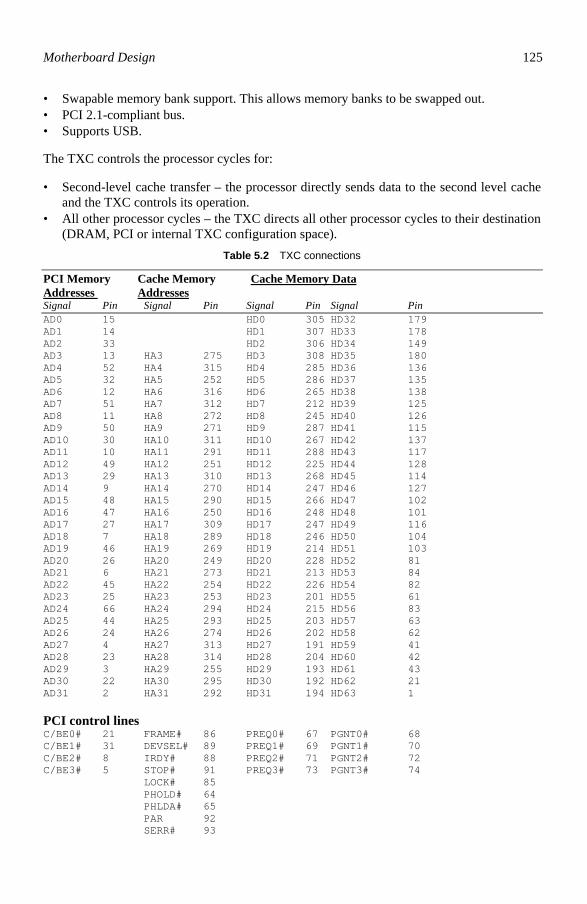
Motherboard Design 125
• Swapable memory bank support. This allows memory banks to be swapped out. • PCI 2.1-compliant bus. • Supports USB. The TXC controls the processor cycles for:
• Second-level cache transfer – the processor directly sends data to the second level cache and the TXC controls its operation.
• All other processor cycles – the TXC directs all other processor cycles to their destination (DRAM, PCI or internal TXC configuration space).
Table 5.2 TXC connections
PCI Memory Cache Memory Cache Memory Data Addresses Addresses Signal Pin Signal Pin Signal Pin Signal Pin AD0 15 HD0 305 HD32 179 AD1 14 HD1 307 HD33 178 AD2 33 HD2 306 HD34 149 AD3 13 HA3 275 HD3 308 HD35 180 AD4 52 HA4 315 HD4 285 HD36 136 AD5 32 HA5 252 HD5 286 HD37 135 AD6 12 HA6 316 HD6 265 HD38 138 AD7 51 HA7 312 HD7 212 HD39 125 AD8 11 HA8 272 HD8 245 HD40 126 AD9 50 HA9 271 HD9 287 HD41 115 AD10 30 HA10 311 HD10 267 HD42 137 AD11 10 HA11 291 HD11 288 HD43 117 AD12 49 HA12 251 HD12 225 HD44 128 AD13 29 HA13 310 HD13 268 HD45 114 AD14 9 HA14 270 HD14 247 HD46 127 AD15 48 HA15 290 HD15 266 HD47 102 AD16 47 HA16 250 HD16 248 HD48 101 AD17 27 HA17 309 HD17 247 HD49 116 AD18 7 HA18 289 HD18 246 HD50 104 AD19 46 HA19 269 HD19 214 HD51 103 AD20 26 HA20 249 HD20 228 HD52 81 AD21 6 HA21 273 HD21 213 HD53 84 AD22 45 HA22 254 HD22 226 HD54 82 AD23 25 HA23 253 HD23 201 HD55 61 AD24 66 HA24 294 HD24 215 HD56 83 AD25 44 HA25 293 HD25 203 HD57 63 AD26 24 HA26 274 HD26 202 HD58 62 AD27 4 HA27 313 HD27 191 HD59 41 AD28 23 HA28 314 HD28 204 HD60 42 AD29 3 HA29 255 HD29 193 HD61 43 AD30 22 HA30 295 HD30 192 HD62 21 AD31 2 HA31 292 HD31 194 HD63 1 PCI control lines C/BE0# 21 FRAME# 86 PREQ0# 67 PGNT0# 68 C/BE1# 31 DEVSEL# 89 PREQ1# 69 PGNT1# 70 C/BE2# 8 IRDY# 88 PREQ2# 71 PGNT2# 72 C/BE3# 5 STOP# 91 PREQ3# 73 PGNT3# 74 LOCK# 85 PHOLD# 64 PHLDA# 65 PAR 92 SERR# 93

126 Computer busses
Cache Memory Parity Address Tag Lines Signal Pin Signal Pin Signal Pin Signal Pin CTAG0 207 MP0 133 MD32 74 CTAG1 260 MP1 123 MD33 75 CTAG2 261 MP2 146 MA2 317 MD34 76 CTAG3 281 MP3 113 MA3 297 MD35 76 CTAG4 238 MP4 132 MA4 277 MD36 76 CTAG5 282 MP5 124 MA5 257 MD37 76 CTAG6 302 MP6 134 MA6 237 MD38 76 CTAG7 322 MP7 122 MA7 298 MD39 76 CTAG8 303 MA8 258 CTAG9 323 MA9 319 CTAG10 324 MA10 318 MA11 278
Cache address lines MRASR0# 121 MCASR0# 145 MAA0 300 MRASR1# 110 MCASR1# 159 MAA1 300 MRASR2# 109 MCASR2# 131 MAB0 300 MRASR3# 96 MCASR3# 173 MAB1 300 MCASR4# 130 MCASR5# 144 MCASR6# 120 MCASR7# 172
Cache control lines CBWE# 321 COE# 259 CCS# 300 CADS# 299 CGWE# 320 CADV# 279
5.1.4 82091AA (AIP)
The AIP device integrates the serial ports, parallel ports and floppy disk interfaces. Figure 5.3 shows its connections and Figure 5.4 shows the interconnection between the AIP and the PIIX3 device. The OSC frequency is set to 14.218 18 MHz. It can be seen that the range of interrupts for the serial, parallel and floppy disk drive is IRQ3, IRQ4, IRQ5, IRQ6 and IRQ7. Normally the settings are: • IRQ3 – secondary serial port (COM2/COM4). • IRQ4 – primary serial port (COM1/COM3). • IRQ6 – floppy disk controller. • IRQ7 – parallel port (LPT1). Figure 5.4 shows the main connections between the TXC, PIIX3 and the AIP. It can be seen that the AIP uses many of the ISA connections (such as 0WS#, IOCHRDY, and so on). The interface between the TCX and the PIIX3 defines the PCI bus and the interface between the PIIX3 and AIP defines some of the ISA signals.

Motherboard Design 127
82091AA (API)
-DSKCHG
74
-SIDE1
75
-RDATA
76
-WPT
77
-TRK0
78
-WGATE
79
-WDATA
80
-STEP
81
-DIR
82
-MOTEB
83
-DRVSA
84
-DRVSB
85
-MOTEA
86
-INDEX
87
-DRATE0
90
-FDDEN
89
-CTS1
-RI1
50
48
-RTS1
-TX1
47
46
-DSR1
-RX1
45
44
-DCD1
43
-DTR1
49
-CTS0
-RI0
42
40
-RTS0
-TX0
39
38
-DSR0
-RX0
37
36
-DCD0
35
-DTR0
41
-INTR
-AutoF
42
40
-ERR
-SLIN
39
38
BUSY
-ACK
37
36
35
-STR
41
PE
35
69
SLCT
D0
67
D1
65
D2
60
D3
58
D4
57
D5
56
D6
55
D7
SA10
17151210 8 7 5 4 3 2 1
SA9
SA8
SA7
SA6
SA5
SA4
SA3
SA2
SA1
SA0
SD7
32
SD6
31
SD5
30
SD4
29
SD3
27
SD2
26
SD1
25
SD0
24
-0WS
23
IOCHRDY
22
AEN
21
-IOWC
20
-IORC
19
-IO16
96
TC
6
DRQ5
100
-DACK5
99
DRQ2
98
-DACK2
97
IRQ7
18
IRQ6
16
IRQ5
13
IRQ4
11
IRQ3
9
RSTDRV
33
X1/OSC
63
Floppy diskinterface
Secondary serialport interface
Primary serialport interface
Parallel portinterface
DMA Interruptlines
ISAhandshaking
Datalines
Addresslines
Figure 5.3 API IC
PIIX3
SA[10:0]
SD[7:0]
OWS#
IOCHRDY
AEN
XIOW#
XIOR#
T/C
IRQ[15:0]
DRQ[7:0]
DACK#[7:0]
RSTDRV
AD[31:0]
C/BE#[3:0]
PIRQ[3:0]
PGNT[1:0]
FRAME#
TRDY#
IRDY#
STOP#
DEVSEL#
SERR#
PHLDA#
HFERR#
EXTSMI#
IOCS16#, IOCHK#
DSKCHG#SIDE1#
FDDEN
RI1#CTS1#
DCD1#
RI0#CTS0#
DCD0#
PD[7:0]STR#
SLCT
Diskdrive
Secondaryserialport
Primaryserialport
Parallelport
TXC
FRAME#
PREQ[3:0]
PHOLD#
PCIRST#
IDE
LA[23:17]
DD[15:0]
Control lines
HINTR
HSMI#
HSTPC
HIGNNG#
BALE, MEMCS16
REFRESH#, SYSCLK
AIPSMEMW#, SMEMR#
SMEMR#,
HD[63:0]
HA[31:0]
HBE#[7:0]
Control
MEMR#, MEMW#
Figure 5.4 Connections between TXC, PIIX3 and AIP

128 Computer busses
5.1.5 DRAM interface
The DRAM interface supports from 4 MB to 512 MB with eight RAS lines (RAS0–RAS7) and a 64-bit data path with eight parity bits. It can use either a 3.3 V or a 5 V power supply and both standard page mode and extended data out (EDO) memory are supported with a mixture of memory sizes for 1 MB, 2 MB and 4 MB-deep SIMMs and symmetrical address-ing for 16 MB-deep SIMMs. Each SIMM (single in-line memory module) has 12 input address lines and has a 32-bit data output. They are normally available with 72 pins (named tabs) on each side. These pins can read the same signal because they are shorted together on the board. For example, tab 1 (pin 1) on side A is shorted to tab 1 on side B. Thus, the 144 tabs only gives 72 useable sig-nal connections. Figure 5.5 shows how the DRAM memory is organized. It shows bank 1 and 2 (and does not show banks 3 and 4). Each bank has two modules, such as modules 0 and 1 are in bank 0. The bank is selected with the MRAS lines, for example bank 1 is selected with MRAS0 and MRAS1, bank 1 by MRAS2 and MRAS3, and so on. An even-numbered module gives the lower 32 bits (MD0–MD31) and the odd number modules give the upper 32 bits (MD32–MD63). Each module also provides four parity bits (MP0–MP3 and MP4–MP7). DIMMs (dual in-line memory modules) have independent signal lines on each side of the module and are available with 72 (36 tabs on each side), 88 (44 tabs on each side), 144 (72 tabs on each side), 168 (84 tabs on each side) or 200 tabs (100 tabs on each side). They give greater reliability and density and are used in modern high performance PC servers.
-RAS0-RAS1-RAS2-RAS3-CAS0-CAS1-CAS2-CAS3
MCAS0MCAS1MCAS2MCAS3
MRAS0MRAS1MRAS0MRAS1
MD0-MD31
MD32-MD63
MA0-MA11
MA0-MA11
MCAS4MCAS5MCAS6MCAS7
MRAS0MRAS1MRAS0MRAS2
-WMWE
-WMWE
MCAS0MCAS1MCAS2MCAS3
MRAS2MRAS3MRAS2MRAS3
MA0-MA11
MA0-MA11
MCAS4MCAS5MCAS6MCAS7
MRAS2MRAS3MRAS2MRAS3
-WMWE
-WMWE
Bank 1 Bank 2
Module 0
Module 1
Module 2
Module 2MP4-P7
MD32-MD63
MP4-P7
MP0-P3
MD0-MD31
MP0-P3
-RAS0-RAS1-RAS2-RAS3-CAS0-CAS1-CAS2-CAS3
-RAS0-RAS1-RAS2-RAS3-CAS0-CAS1-CAS2-CAS3
-RAS0-RAS1-RAS2-RAS3-CAS0-CAS1-CAS2-CAS3
Figure 5.5 DRAM memory interface

Motherboard Design 129
5.1.6 Clock rates
The system board runs at several clock frequencies. These are: • Processor speed – the processor, TXC and SRAM run at the system frequency (such as
66 MHz), • PCI bus speed – TCX, PIIX3 and PCI slots. • 24 or 48 MHz – USB (Universal Serial Bus). • 12 MHz – keyboard. • 24 MHz – floppy clock. • 14 MHz – ISA bus OSC. • 8 MHz – ISA bus clock.
5.1.7 ISA/IDE interface
The IDE and ISA buses share several data, address and control lines. Figure 5.6 shows the connections to the buses. The IDE interface uses the DD[12:0] and LA[23:17] lines, and the ISA uses these lines as SBHE#, SA[19:8, CS1S, CS3S, CS1P, CS3P and DA[2:0]. A multi-plexor (MUX) is used to select either the ISA or IDE interface lines.
5.1.8 DMA interface
The PIIX3 device incorporates the functionality of two 8237 DMA controllers to give seven independently programmable channel (channels 0–3 and Channels 5–7). DMA channel 4 is used to cascade the two controllers and defaults to cascade mode in the DMA channel mode (DCM) register. Figure 5.7 shows the interface connections.
ISA
SD[15:0]IOCS16#MEMCS16#MEMR#MEMW#AENIOCHRDYIOCHK#SYSCLKBALEIOR#IOW#SMEMR#SMEMW#0WS#SA[7:0]
MUX
DD[11:0]/SA[19:8]LA23/CS16LA22/CS3SLA21/CS1PLA20/CS3PLA[19:17]/DA[2:0]
DD12/SBHE#
DIOR#DIOW#DDRQ[1:0]DDAK[1:0]#IORDYSOE#SDIRDD13
IDE
PIIX3
Figure 5.6 IDE/ISA interface with PIIX3

130 Computer busses
DMADREQ[7:5,3:0]DACK[7:5.3:0]TCREFRESH#
PIIX3
Figure 5.7 DMA interface
5.1.9 Interval timer
The PIIX3 contains three 8251-compatible counters. The three counters are contained in one PIIX3 timer unit, referred to as Timer 1. Each counter provides an essential system function. The functions of the counters are: • Counter 0 – connects to the IRQ0 line and provides a system timer interrupt for a time-of-
day, diskette time-out, and so on. The input to the counter is a 14.218 18 MHz clock (OSC). This is then used to increment a 16-bit register, which rolls over every 55 ms.
• Counter 1 – generates a refresh request signal. • Counter 2 – generates the speaker tone.
5.1.10 Interrupt controller
The PXII3 incorporates two 8259-compatible interrupt controllers which provide an ISA- compatible interrupt controller. These are cascaded to give 13 external and three internal in-terrupts. The primary interrupt controller connects to IRQ0–IRQ7 and the secondary con-nects to IRQ8–IRQ15. The three internal interrupts are: • IRQ0 – used by the system timer and is connected to Timer 1, Counter 0. • IRQ2 – used by the primary and secondary controller (see Figure 2.2 in Section 2.3.2). • IRQ13 – used by the math coprocessor, which is connected to the FERR pin on the
processor. Figure 5.8 shows that the PC uses IRQ0 as the system timer and IRQ2 by the programmable interrupt controller. The interrupt unit also supports interrupt steering. The four PCI active low interrupts (PIRQ#[D:A]) can be internally routed in the PIIX3 to one of 11 interrupts (IRQ15, IRQ14, IRQ12–IRQ9, IRQ7–IRQ3).
5.1.11 Mouse function
The mouse normally either connects to one of the serial ports (COM1: or COM2:) or a PS/2-type connector. If they connect to the PS/2-type connector then IRQ12 is used, else a serial port connected mouse uses the serial interrupts (such as IRQ4 for COM1 and IRQ3 for COM2). Thus, a system with a serial connected mouse must have the IRQ12/M interrupt dis-abled. This is normally done with a motherboard jumper (to enable or disable the mouse in-terrupt). Figure 5.8 shows an example of a mouse using IRQ12.

Motherboard Design 131
Figure 5.8 Interrupts usage shows PS/2 port mouse
5.1.12 Power management
PIIX3 has extensive power management capability permitting a system to operate in a low power state without being powered down. In a typical desktop PC there are two states – power on and power off. Leaving a system powered on when not in use wastes power. PIIX3 provides a fast on/off feature that creates a third state called fast off. When in the fast off state, the system consumes less power than the power on state. The PIIX3’s power management function is based on two modes:
• System management mode (SMM). • Advanced power management (APM). Software (called SMM code) controls the transitions between the power on state and the fast off state. PIIX3 invokes this software by generating an SMI (system management interrupt) to the CPU (asserting the SMI signal). The SMM code places the system in either the power on state or the fast off state.
5.1.13 Graphics subsystem
The 430HX incorporates the S3 ViRGE graphics device with 2 MB of graphics memory, which has:
• High performance 64-bit 2D/3D graphics engine.
• RAMDAC/clock synthesiser capable of pixel rates of 135 MHz.
• S3 streams processor, enabling the device to convert YUV formatted video data to RGB format.
• 3D features including flat shading and texture mapping support.
• Fast linear addressing scheme.
• VESA (Video Electronics Standards Association) capability.

132 Computer busses
5.2 TX motherboard
The Intel 430HX motherboard only supports up to 128 MB of memory and has a relatively small second level cache (256 kB). The Intel 430TX board has many enhanced devices, such as standardised USB connections and enhanced super I/O device. Figure 5.9 shows the main layout. The 430TX board uses 168-pin DIMM sockets for memory addition. It supports both EDO DRAM and SDRAM (synchronous DRAM). SDRAM synchronous data transfers using the system clock. This simplifies memory timing, leading to an increase in memory transfer. The 430TX motherboard supports a 64-bit data path to memory. The 430TX board uses the 82430TX PCI chipset, which has:
• 82439TX Xcelerated Controller (MTXC), which replaces the TXC (82439HX) in the HX board.
• 82371AB PCI/ISA IDE Xcelerator (PIIX4), which replaces the PIIX3 (82371SB) in the HX board. This is a 324-pin BGA that integrates PCI-to-ISA bridge (two 82C37 DMA controllers, two 82C59 interrupt controllers, an 82C54 timer/counter and a real-time clock), PCI/IDE interface, USB host/hub function and power management functions.
ISA connectors
PCI connectors
DIMMsockets
IDEconnectors
Graphicscontroller
82430TXSystemController
82430TXPCI/ISA/IDEXcelerator (PIIX4)
Level 2 cacheSRAM
Audiocodec
Audio(OP4-ML)
Pentiumprocessor
TV-outdevice
Videomemory
Flashmemorydevice
PC87307ULI/O Controller
Videocaptureprocessor
Figure 5.9 AN430TX board
5.2.1 PIIX4
The PIIX4 supports two types of PCI DMA protocol, PC/PCI DMA which uses dedicated request and grant signals to permit PCI devices to request transfers associated with specific

Motherboard Design 133
DMA channels, and distribute DMA which is based on monitoring CPU accesses to the 8237 controller (this was not implemented on the PIIX3). The PIIX4 also supports Ultra DMA/33 Synchronous DMA mode transfers up to 33MB/s. Ultra DMA is a newer protocol for the IDE hard drive interface that doubles the burst data rate from 16.6 MB/s (as supported by the PIIX3). Ultra DMA widens the path to the hard drive by transferring twice as much data per clock cycle, so doubling the perform-ance. The Ultra DMA protocol lets host computers send and receive data faster, removing bottlenecks associated with data transfers. In addition to speed improvements, the protocol brings new data integrity capabilities to the IDE interface such as improved timing margins and data protection verification. Ultra DMA protocol also allows drives and system to retain backward compatibility with the pre-vious ATA standard.
Real time clock
The real-time clock provides a data-and-time keeping device with alarm features and battery- backed operation. The RTC counts seconds, minutes, hours, days, day of the week, date, month and year. It counts 256 bytes of battery-backed SRAM in two banks. The RTC mod-ule requires an external oscillator source of 32.768 kHz connected between TXCX1 and RTCX2.
5.2.2 I/O controller
The PC87306B I/O controller is similar to the 82091AA (AIP) used in the 430HX board. It has:
• Floppy disk interface – provides support for several different floppy disk capacities and sizes.
• Multimode parallel port – supports for output only compatibility mode, bidirectional mode, EPP mode and ECP mode.
• Two FIFO serial ports. Giving transfers rates up to 921Kbps.
• Real-time clock – provides time-of-day, 100-year calendar and alarm features.
• Keyboard and mouse controller – keyboard and mouse interfaces (as well as power on/reset password protection).
• Infrared support – connection to infrared transmitter/receiver.
5.2.3 Graphics subsystem
The 430HX incorporates the ATI-241 Rage II+ graphics controller which has:
• Drawing coprocessor that operates concurrently with the host processor.
• Video coprocessor.
• Video scalar, colour space converter, true colour palette.
• ATI multimedia.
• Enhanced power features.
• VGA/VESA capability. The 430HX also has an optional video capture processor for digitising analogue inputs from

134 Computer busses
VCRs, cameras, TVs, and so on. It also has an optional ATI-ImpactTC NSTC/PAL encoder which provides a TV output for the graphics accelerators.
5.2.4 DRAM interface
The DRAM interface is a 64-bit data path that supports fast page mode (FPM) and extended data out (EDO) memory. The integrated DRAM controller supports from 4 MB to 256 MB of main memory. The 12 multiplexed address lines (MA[11:0]) allow the chips to support 4-bit, 16-bit and 64-bit memory, both symmetrical and asymmetrical addressing. The MTXC has six RAS lines which enables support to up to six rows of DRAM (the TXC has eight RAS lines). The MTXC supports SRAM. The 14 multiplexed address lines (MA[13:0]) allow the MTXC to support 16-bit and 64-bit SDRAM devices. The MTXC has six CS (chip select) lines (muxed into RAS[5:0]) which allows six rows of the faster SDRAM modules to be in-stalled. All these memory types FPM, EDO and SDRAM can be mixed on the 430TX (but only the FPM and EDO are supported in the 430HX board). The extra lines that have been added in the MTXC are: • SRAS [A,B] – SRAM row address strobe. • SCAS [A,B] – DRAM column address.
5.2.5 Second- level cache
The MTXC supports cache memory area of 64 MB using either 8 K×8 or 16 K×8 SRAM blocks to store the cache tags for either 256 KB or 512 KB SRAM cache. (8 K×8 is used for 256 KB and 16 K×8 is used for 512 KB). Each cache entry is 32 bits (4 bytes) thus the total cache memory size is 512 KB (16 K×8×4). The signals are:
CCS Cache chip select – set active upon power-up and allows access to the cache.
TWE Tag write enable – allows new state and tag addresses to be written into the cache.
COE Cache output enable – puts the cache data onto the data bus.
GWE Global write enable – causes all bytes to be written to.
CADS Cache address strobe – cache loads the address register from the ad-dress pins.
CADV Cache advance – the address is automatically increment to the next word.
0]:TIO[7 Tag address – input lines for tag addresses.
CS4_64KRQAK/ . Cache chip select – KRQAK specifies DRAM cache, else implements a 64 MB main memory cache.
BWE Byte write enable – enables up to eight bytes from the data bus. Figure 5.10 shows the interface between the MTXC and the second-level cache. Note that four 32 K×32 devices make up the 512 KB (4×32×4) SRAM cache. Only two are shown in Figure 5.10, as the other two are connected in parallel with the two shown.

Motherboard Design 135
GWE#BWE#BE[3:0]#
D[31:24]
D[23:16]
D[15:8]
D[7:0]
HD[31:24]HD[23:16]HD[15:8]HD[7:0]
CLKA[14:0]OE#CS1#ADSC#ADV#ADSP#CS2CS2#GWE#BWE#BE[3:0]#
D[7:0]
WE#
OE#
A[13:0]
TIO[7:0]
TWE#
HA[17:3]
ADS#]HA18GND]
HBE[7:4]#
COE#CCS#CADS#CADV#
GWE#BWE#
HA[18:5]
HCLK]
32K×32 SRAM
16K×8 Tag RAMMTXC
D[31:24]
D[23:16]
D[15:8]
D[7:0]
HD[63:56]HD[55:48]HD[47:40]HD[39:32]
HBE[3:0]#
Figure 5.10 Second-level cache interface
Cache control register (CC)
This is an 8-bit register which is located at 52h in the I/O memory. It defines secondary cache operations. Its format is:
Bit Description 7:6 Secondary cache size – 00 (disabled), 01 (256K), 10 (512K), 11 (reserved). 5:4 SRAM cache type – 00 (pipelined burst SRAM), 01 (reserved), 10 (re-
served), 11 (two banks of pipelined burst). 3 NA disable – 1 (disable), 0 (enabled); normally enabled. 2 Reserved. 1 Secondary cache force miss or invalidated (SCFMI). When set to a 1, the
Level 2 hit/miss facility is disabled, else it is enabled. 0 First-level cache enable (FLCE) – 1 (enable), 0 (disable). When it is set to a
1, the control responds to processor cycles with KEN# active. Normal mode for FLCE, SCFMI is 1, 0.
Extended cache control register (CEC)
This is an 8-bit register which is located at 53h in the I/O memory. It defines the refresh rate for DRAM Level 2. Its format is:

136 Computer busses
Bit Description 7:6 Reserved. 5 Defines if DRAM cache is present – 1 (present), 0 (not present). 4:0 DRAM cache refresh timer value.
5.2.6 Power management
The PIIX4 has enhanced power management over the PIIX3 and can detect when a specific device is idle. The system management software is then informed, which then can place the idle device into a power managed condition (such as local standby or powered off). Accesses targeted to that device are then monitored. When detected, an SMI is generated to allow the software to restore the device to operation. The PIIX4 supports the Advanced Configuration and Power Interface (ACPI) specifica-tion. The software consists of system management mode (SMM) BIOS for legacy control and operating system for ACPI. The basic operation consists of software setting up the de-sired configurations and power management mode and corresponding power saving levels. The hardware then performs the necessary actions to maintain the power mode. The I/O chip also monitors the system for events which may require changing the system power mode.
5.3 Exercises 5.3.1 The data bus signals which connect to the processor are: (a) HD0–HD63 (b) D0–D63 (c) HA0–HA63 (d) AD0–AD63 5.3.2 Which device provides the bridge between the processor, second-level cache,
DRAM and the PCI bus: (a) PIIX3/4 (b) HXC (c) RFC/MRFC (d) TXC/MTXC 5.3.3 Which device provides the bridge between the PCI bus and other busses, such as
the IDE, ISA and USB: (a) PIIX3/4 (b) HXC (c) RFC (d) TXC 5.3.4 The maximum achievable data throughput for a 33 MHz, 32-bit PCI is 132 MB/s.
Why is this not achievable in the normal multiplexed mode: (a) Half of the bus is used for addresses, the other half for data (b) The bus must slow down because of synchronisation problems (c) The address and data line are shared (multiplexed address then data). (d) The clock rate is halved for all transfers 5.3.5 How does a cache identify the address of the data it has in its memory: (a) The full address is stored along with the data (b) It is tagged (CTAG).

Motherboard Design 137
(c) It guesses the address (d) It checks the address with the contents of the DRAM 5.3.6 How many data bits are transferred between the processor and the second-level
cache: (a) 16 (b) 32 (c) 64 (c) 128 5.3.7 Outline the importance of the TXC (system controller) device in the PC. Outline
also the main ICs that are used in a PC. 5.3.8 Describe, in detail, the architecture of the HX PCI chip set, and how the Pentium
processor communicates with: DRAM memory, Level-2 SRAM cache, the PCI bus, the ISA bus and the IDE bus.
5.3.9 Explain, with reference to the PIIX3 and Pentium processor, how interrupts on the
PCI and ISA busses are dealt with. 5.3.10 Explain, with reference to the level-1 cache, the level-2 cache and DRAM, how
the processor accesses memory. What advantage does level-1 have over level-2 cache, and what advantage do these have over DRAM.
5.3.11 Discuss the power management modes supported by the PXII3, and also by the
PXII4. 5.3.12 Which interrupts are supported with the AIP and where are they typically used? 5.3.13 Explain how the ISA and IDE busses share the same control and data lines. 5.3.14 Contrast the HX motherboard with the LX motherboard.
5.4 Notes from the author
I hope that this chapter was not too heavy. It is important to realise that it is not just the speed of the processor that defines the performance of a system – it is the cache controllers, the bridge devices, the PCI bus, and so on. So have tried to give you an understanding of the segmentation that is used in typical PCs. The devices used will change, but the basic concept is likely to stay the same (I hope!). The days of a PC on a chip will happen, someday. The most amazing thing about modern PC systems is that they are almost completely compatible with the original PC, the big change has happened in the integration of many of the components parts. The great strength of the PC is its availability, durability and up-gradeability of its components. I find it amazing that it can disconnect the cable to the disk drives, turn it round, and connect it and the system will not be damage, in any way (although it won’t start). I can even put the processor in the wrong way, and it will not damage it. The other amazing thing about PCs is the way that new peripherals are quickly adopted, and become standard parts of the PC. This has included CD-ROM drives, USB connectors, PS/2-type mouse connectors, PCMCIA connectors (in notebooks), VGA graphics adaptors, TV output, DVD drives, network cards, sound cards, and so on. Who would have believed that such a basic system as the original PC would support all this expansion, without ever the need to redesign it (although the PCI bus provided a new architectural design).

IDE and Mass Storage
6.1 Introduction
This chapter and the next chapter discuss IDE and SCSI interfaces which are used to inter-face to disk drives and mass storage devices. Disks are used to store data reliably in the long term. Typical disk drives either store binary information as magnetic fields on a fixed disk (as in a hard disk drive), a plastic disk (as in a floppy disk or tape drive), or as optical repre-sentation (on optical disks). The main sources of permanent read/writeable storage are: • Magnetic tape – where the digital bits are stored with varying magnetic fields. Typical
devices are tape cartridges, DAT and 8 mm video tape. • Magnetic disk – as with the magnetic tape the bits are stored as varying magnetic fields
on a magnetic disk. This disk can either be permanent (such as a hard disk) or flexible (such as a floppy disk). Large capacity hard disks allow storage of several gigabytes of data. Normally fixed disks are designed to a much higher specification than floppy disks and can thus store much more information.
• Optical disk – where the digital bits are stored as pits on an optical disk. A laser then reads these bits. This information can either be read only (CD-ROM), write once read many (WORM) or can be reprogrammable. A standard CD-ROM stores up to 650 MB of data. Their main disadvantage in the past has been their relative slowness as compared with Winchester hard disks; this is now much less of a problem as speeds have steadily increased over the years.
6.2 Tracks and sectors
A disk must be formatted before it is used, which allows data to be stored in a logical man-ner. The format of the disk is defined by a series of tracks and sectors on either one or two sides. A track is a concentric circle around the disk where the outermost track is track 40 and the innermost track is 0. The next track is track 1 and so on, as shown in Figure 6.1. Each of these tracks is divided into a number of sectors. The first sector is named sector 1, the second is sector 2, and so on. Most disks also have two sides: the first side of the disk is called side 0 and the other is side 1.
6

140 Computer busses
Track 0
Track 40
Sector 1 (512 bytes)
Sector 2(512 bytes)
Figure 6.1 Tracks and sectors on a disk
Figure 6.1 also shows how each track is split into a number of sectors, in this case there are eight sectors per track. Typically each sector stores 512 bytes. The total disk space, in bytes, will thus be given by
Disk space = Number of sides × tracks × sectors per track × bytes per sector For example, a typical floppy disk has two sides, 80 tracks per side, 18 sectors per track and 512 bytes per sector, so
Disk capacity = 2×80×18×512 = 1 474 560 B = 1 474 560/1 024 KB = 1 440 KB = 1440/1024 MB = 1.4 MB
6.3 Floppy disks
A 3.5-inch DD (double density) disk can be formatted with two sides, nine sectors per track and 40 tracks per side. This gives a total capacity of 720 KB. A 3.5 inch HD (high density) disk has a maximum capacity when formatted with 80 tracks per side. A 5.25-inch DD disk can be formatted with two sides, nine sectors per disk with either 40 or 80 tracks per side. The maximum capacity of these formats is 360 KB (40 tracks) or 720 KB (80 tracks). A 5.25-inch HD disk can be formatted with 15 sectors per track which gives a total capacity of 1.2 MB. When reading data the disks rotate at 300 rpm. Table 6.1 outlines the differing formats.
Table 6.1 Capacity of different disk types
Size Tracks per side Sectors per track Capacity 5.25 -inch 40 9 360 KB 5.25-inch 80 15 1.2 MB 3.5-inch 40 9 720 KB 3.5-inch 80 18 1.44 MB

IDE and mass storage 141
6.4 Fixed disks
Fixed disks store large amounts of data and vary in their capacity, from several MB to sev-eral GB. A fixed disk (or hard disk) consists of one or more platters which spin at around 3000 rpm (10 times faster than a floppy disk). A hard disk with four platters is shown in Fig-ure 6.2. Data is read from the disk by a flying head which sits just above the surface of the platter. This head does not actually touch the surface as the disk is spinning so fast. The dis-tance between the platter and the head is only about 10µin (which is no larger than the thick-ness of a human hair or a smoke particle). It must thus be protected from any outer particles by sealing it in an airtight container. A floppy disk is prone to wear as the head touches the disk as it reads but a fixed disk has no wear as its heads never touch the disk. One problem with a fixed disk is head crashes, typically caused when the power is abruptly interrupted or if the disk drive is jolted. This can cause the head to crash into the disk surface. In most modern disk drives the head is automatically parked when the power is taken away. Older disk drives that do not have automatic head parking require a program to park the heads before the drive is powered down. There are two sides to each platter and, like floppy disks, each side divides into a number a tracks which are subdivided into sectors. A number of tracks on fixed disks are usually named cylinders. For example a 40 MB hard disk has two platters with 306 cylinders, four tracks per cylinder, 17 sectors per track and 512 bytes per sector, thus each side of a platter stores 306×4×17×512 B = 10 653 696 B = 10 653 696/ 1 048 576 MB = 10.2 MB
Platters
Read/write heads
Head movement
Figure 6.2 Hard disk with four platters

142 Computer busses
6.5 Drive specifications
Access time is the time taken for a disk to locate data. Typical access times for modern disk drives range from 10 to 30 ms. The average access time is the time for the head to travel half way across the platters. Once the head has located the correct sector then there may be an-other wait until it locates the start of the data within the sector. If it is positioned at a point after the start of the data, it requires another rotation of the disk to locate the data. This aver-age wait, or latency time, is usually taken as half of a revolution of the disk. If the disk spins at 3600 rpm then the latency is 8.33 ms. The main parameters which affect the drive specification are the data transfer rate and the average access time. The transfer rate is dependent upon the interface for the controller/disk drive and system/controller and the access time is dependent upon the disk design.
6.6 Hard disk and CD-ROM interfaces There are two main interfaces involved with a hard disks (and CD-ROMs). One connects the disk controller to the system (system–controller interface) and the other connects the disk controller to the disk drive (disk–controller interface). The controller can be interfaced by standards such as ISA, EISA, MCA, VL-Local bus or PCI bus. For the interface between the disk drive and the controller then standards such as ST-506, ESDI, SCSI or IDE can be used. ST-506 was developed by Seagate Technologies and is used in many older machines with hard disks of a capacity less than 40 MB. The en-hanced small disk interface (ESDI) is capable of transferring data between itself and the processor at rates approaching 10 MB/s. The small computer system interface (SCSI) allows up to seven different disk drives or other interfaces to be connected to the system through the same interface controller. SCSI is a common interface for large capacity disk drives and is illustrated in Figure 6.3. The most popular type of PC disk interface is the integrated drive electronics (IDE) stan-dard. It has the advantage of incorporating the disk controller in the disk drive, and attaches directly to the motherboard through an interface cable. This cable allows many disk drives to be connected to a system without worrying about bus or controller conflicts. The IDE inter-face is also capable of driving other I/O devices besides a hard disk. It also normally contains at least 32K of disk cache memory. Common access times for an IDE are often less than 16 ms, where as access times for a floppy disk are about 200 ms. With a good disk cache system the access time can reduce to less than 1 ms. A comparison of the maximum data rates is given in Table 6.2.
Table 6.2 Capacity of different disk types
Interface Maximum data rate (MB/s) Interface Maximum data rate (MB/s) ST-506 0.6 E-IDE 16.6 ESDI 1.25 SCSI 4 .0 IDE 8.3 SCSI-II 10.0

IDE and mass storage 143
Peripheral
Controller1
Peripheral
Controller2
Peripheral
Controller7
SCSI hostadapter
System data bus
System address bus
Common SCSI connection
Figure 6.3 SCSI interface
A typical modern PC contains two IDE connections on the motherboard, named IDE0 and IDE1. The IDE0 connection connects to the master drive (C:) and IDE1 to the slave drive (D:). These could connect either to two hard disks or, possibility, to one hard disk and a CD-ROM drive (or even a tape backup system). Unfortunately, the IDE standard only allows disk access up to 528 MB. A new standard called Enhanced-IDE (E-IDE) allows for disk capacities of over this limit. The connector used is the same as IDE but the computers’ BIOS must be able to recognise the new standard. Most computers manufactured since 1993 are able to fully access E-IDE disk drives. The specifications for the IDE and EIDE are IDE
• Maximum of two devices (hard disks). • Maximum capacity for each disk of 528 MB. • Maximum cable length of 18 inches. • Data transfer rates of 3.3, 5.2 and 8.3 MB/s.
EIDE • Maximum of four devices (hard disks, CD-ROM and tape). • Uses two ports (for master and slave). • Maximum capacity for each disk is 8.4 GB. • Maximum cable length of 18 inches. • Data transfer rates of 3.3, 5.2, 8.3, 11.1 and 16.6 MB/s.
6.7 IDE interface
The most popular interface for hard disk drives is the Integrated Drive Electronics (IDE) interface. Its main advantage is that the hard disk controller is built into the disk drive and the interface to the motherboard simply consists of a stripped-down version of the ISA bus. The most common standard is the ANSI-defined ATA-IDE standard. It uses a 40-way ribbon cable to connect to 40-pin header connectors. Table 6.3 lists the pin connections. It has a 16-bit data bus (D0–D15) and the only available interrupt line used is IRQ14 (the hard disk uses

144 Computer busses
IRQ14). The standard allows for the connection of two disk drives in a daisy-chain configuration. This can cause problems because both drives have controllers within their drives. The pri-mary drive (Drive 0) is assigned as the master and the secondary driver (Drive 1) as the slave. A drive is set as a master or a slave by setting jumpers on the disk drive. They can also be set by software using the cable select (CSEL) pin on the interface. EIDE has various modes (ANSI modes) of operation, these are • Mode 0 – 600 ns read/write cycle time, 3.3 MB/s burst data transfer rate. • Mode 1 – 383 ns read/write cycle time, 5.2 MB/s burst data transfer rate. • Mode 2 – 240 ns read/write cycle time, 8.3 MB/s burst data transfer rate. • Mode 3 – 180 ns read/write cycle time, 11.1MB/s burst data transfer rate. • Mode 4 – 120 ns read/write cycle time, 16.6MB/s burst data transfer rate.
Table 6.3 IDE connections
Pin IDE signal AT signal Pin IDE signal AT signal 1 RESET RESET DRV 2 GND – 3 D7 SD7 4 D8 SD8 5 D6 SD6 6 D9 SD9 7 D5 SD5 8 D10 SD10 9 D4 SD4 10 D11 SD11 11 D3 SD3 12 D12 SD12 13 D2 SD2 14 D13 SD13 15 D1 SD1 16 D14 SD14 17 D0 SD0 18 D15 SD15 19 GND – 20 KEY – 21 DRQ3 DRQ3 22 GND – 23 IOW IOW 24 GND – 25 IO R IO R 26 GND – 27 IOCHRDY IOCHRDY 28 CSEL – 29 DACK3 DACK3 30 GND – 31 IRQ14 IRQ14 32 IOCS16 IOCS16 33 Address bit 1 SA1 34 PDIAG – 35 Address bit 0 SA0 36 Address bit 2 SA2 37 CS1FX – 38 CS3FX – 39 SP / DA – 40 GND –
6.8 IDE communication
The IDE (or AT bus) is the de facto standard for most hard disks in PCs. It has the advantage over older type interfaces that the controller is integrated into the disk drive. Thus the com-puter only has to pass high-level commands to the unit and the actual control can be achieved with the integrated controller. Several companies developed a standard command set for an ATA (AT attachment). Commands include: • Read sector buffer – reads contents of the controller’s sector buffer. • Write sector buffer – writes data to the controller’s sector buffer.

IDE and mass storage 145
• Check for active. • Read multiple sectors. • Write multiple sectors. • Lock drive door. The control of the disk is achieved by passing a number of high-level commands through a number of I/O port registers. Table 6.3 outlined the pin connections for the IDE connector. Typically pin 20 is missing on the connector cable so that it cannot be inserted the wrong way, although most systems buffer the signals so that the bus will not be damaged if the ca-ble is inserted the wrong way. The five control signals which are unique to the IDE interface (and not the AT bus) are • CS3FX , CS1FX – these are used to identify either the master or the slave. • PDIAG (passed diagnostic) – used by the slave drive to indicate that it has passed its di-
agnostic test. • SP / DA (slave present/drive active) – used by the slave drive to indicate that it is present
and active. The other signals are • IOCHRDY – This signal is optional and is used by the drive to tell the processor that it re-
quires extra clock cycles for the current I/O transfer. A high level informs the processor that it is ready, while a low informs it that it needs more time.
• DRQ3, DACK3 – These are used for DMA transfers.
6.8.1 AT task file
The processor communicates with the IDE controller through data and control registers (typi-cally known as the AT task file). The base registers used are between 1F0h and 1F7h for the primary disk (170h and 177h for secondary), and 3F6h (376h for secondary), as shown in Figure 6.4. Their function is:
Port Function Bits Direction 1F0h Data register 16 R/W 1F1h Error register 8 R Precompensation 8 W 1F2h Sector count 8 R/W 1F3h Sector number 8 R/W 1F4h Cylinder LSB 8 R/W 1F5h Cylinder MSB 8 R/W 1F5h Drive/head 8 R/W 1F6h Status register 8 R Command register 8 W 3F6h Alternative status register 8 R Digital output register 8 W 3F7h Drive address 8 R

146 Computer busses
Figure 6.4 Typical hard-disk controller settings for the primary and secondary drive
Data register (1F0h)
The data register is a 16-bit register which is used to read/write data from/to the disk.
Error register (1F1h)
The error register is read-only and contains error information relating to the last command. Its definitions are b7 b6 b5 b4 b3 b2 b1 b0 BBK UNC MC NID MCR ABT NT0 NDM where • BBK – set to 1 if the sector is bad. • UNC – set to 1 if there is an unrecoverable error. • NID – set to 1 if mark not found. • ABT – set to 1 if command aborted. • NT0 – set to 1 if track 0 not found. • MC – set to 1 identifies that the medium has changed (EIDE only). The EIDE standard
support disks which can be changed while the system is running (such as CD-ROMs, tape drives, and so on).
• MCR – set to 1 identifies that the medium requires to be changed (EIDE only).
Sector count register (1F2h)
This is a read/write 8-bit register which defines the number of sectors to be read, written or verified. After each transfer to/from the disk causes the register value to be decremented by one.

IDE and mass storage 147
Sector number register (1F3h)
This is a read/write 8-bit register which defines the start sector to be read, written or verified. After each transfer to/from the disk, the register contains the last processed sector.
Cylinder register (1F4h/1F5h)
These are read/write 8-bit registers which define the LSB (1F4h) and MSB (1F5h) of the cylinder number. The two registers are capable of containing a 16-bit value. In standard IDE the cylinder number is 10-bit and can only vary from 0 to 1023 (0 to 210–1). For E-IDE the value can be a 16-bit value and can thus vary from 0 to 65 535 (0 to 216–1). This is one of the main reasons that E-IDE can address much more data than IDE.
Drive/head register (1F6h)
This is a read/write 8-bit register which defines the currently used head. Its definitions are: b7 b6 b5 b4 b3 b2 b1 b0 1 L 1 DRV HD3 HD2 HD1 HD0 where: • L – set to 1 if LBA (logical block addressing) mode else set to 0 if CHS (EIDE only). • DRV – set to 1 for the slave, else it is master. • HD3–HD0 – identifies the head number, where 0000 identifies head 0, 0001 identifies head
1, and so on.
Status register (1F7h)
The 1F7h register has two modes. If it is written to then it is a command register (see next section) else, if it is read from, then it is a status register. The status register is a read-only 8-bit register which contains status information from the previously issued command. Its defi-nitions are: b7 b6 b5 b4 b3 b2 b1 b0 BUSY RDY WFT SKT DRQ COR IDX ERR where: • BUSY – set to 1 if the drive is busy. • RDY – set to 1 if the drive is ready. • WFT– set to 1 if there is a write fault. • SKT– set to 1 if head seek positioning is complete. • DRQ – set to 1 if data can be transferred. • COR – set to 1 if there is a correctable data error. • IDX – set to 1 identifies that the disk index has just passed. • ERR – set to 1 identifies that the error register contains error information.
Command register (1F7h)
If the 1F7h register is written-to then it is a command register. The command register is a 8-bit register can contain commands, such as:

148 Computer busses
Command b7 b6 b5 b4 b3 b2 b1 b0 Related registers Calibrate drive 0 0 0 1 – – – – 1F6h Read sector 0 0 1 0 – – L R 1F2h–1F6h Write sector 0 0 1 1 – – L R 1F2h–1F6h Verify sector 0 1 0 0 – – – R 1F2h–1F6h Format track 0 1 0 1 – – – – 1F3h–1F6h Seek 0 1 1 1 – – – – 1F4h–1F6h Diagnostics 1 0 0 1 – – – – 1F2h, 1F6h Read sector buffer 1 1 1 0 0 1 0 0 1F6h Write sector buffer 1 1 1 0 1 0 0 0 1F6h Identify drive 1 1 1 0 1 1 – – 1F6h where R is set to 0 if the command is automatically retried and L identifies the long-bit.
Digital output register (3F6h)
This is a write-only 8-bit register which allows drives to be reset and also IRQ14 to be masked. Its definitions are b7 b6 b5 b4 b3 b2 b1 b0 – – – – – SRST IEN – where • SRST– set to a 1 to reset all connected drives, else accept the command. • IEN – controls the interrupt enable. If set to 1 then IRQ14 is always masked, else inter-
rupted after each command.
Drive address register (3F7h)
The drive address register is a read-only register which contains information on which drive and which head is currently active. Its definitions are: b7 b6 b5 b4 b3 b2 b1 b0 – WTGT HS3 HS2 HS1 HS0 DS1 DS0 where • WTGT – set to 1 if the write gate is closed, else the write gate is open. • HS3 – HS0 –1’s complement value of currently active head. • DS1 – DS0 – identifies the selected drive.
6.8.2 Command phase
The IRQ14 line is used by the disk to when it wants to interrupt the processor, either when it wants to read or write data to/from memory. For example, using Microsoft C++ (for Borland replace _outp() and _inp() with outport() and inport()) to write to a disk at cylinder 150, head 0 and sector 7:

IDE and mass storage 149
#include <conio.h> int main(void) int sectors=4, sector_no=7, cylinder=150, drive=0, command=0x33, i; unsigned int buff[1024], *buff_pointer; do /* wait until BSY signal is set to a 1 */ while (( _inp(0x1f7) & 0x80) != 0x80); _outp(0x1f2,sectors); /* set number of sectors */ _outp(0x1f3,sector_no); /* set sector number */ _outp(0x1f4,cylinder & 0x0ff); /* set cylinder number LSB */ _outp(0x1f5,cylinder & 0xf00); /* set cylinder number MSB */ _outp(0x1f6,drive); /* set DRV=0 and head=0 */ _outp(0x1f7,command); /* 0011 0011 (write sector) */ do /* wait until BSY signal is set to a 1 and DRQ is set to a 1 */ while ( ((_inp(0x1f7) & 0x80) != 0x80) && ((_inp(0x1f7) & 0x08) !=0x08) ); buff_pointer= buff; for (i=0;i<512;i++,buff_pointer++) _outp(0x1f0,*buff_pointer); /* output 16-bits at a time */ return(0); Note that if the L bit is set then an extra four ECC (error correcting code) bytes must be writ-ten to the sector (thus a total of 516 bytes are written to each sector). The code used is cyclic redundancy check, which, while it cannot correct errors is very powerful at detecting them.
6.8.3 E-IDE
The main differences between IDE and E-IDE are: • E-IDE support removable media. • E-IDE supports a 16-bit cylinder value, which gives a maximum of 65 636 cylinders. • Higher transfer rates. In mode 4, E-IDE has a 120 ns read/write cycle time, which gives a
16.6 MB/s burst data transfer rate. • E-IDE supports LBA (logical block addressing) which differs from CHS (cylinder head
sector) in that the disk drive appears to be a continuous stream of sequential blocks. The addressing of these blocks is achieved from within the controller and the system does not have to bother about which cylinder, header and sector is being used.
IDE is limited to 1024 cylinders, 16 heads (drive/head register has only four bits for the number of heads) and 63 sectors, which gives
Disk capacity = 1024×16×63×512 = 504 MB With enhanced BIOS this is increased to 1024 cylinders, 256 heads (8-bit definition for the number of heads) and 63 sectors, to give
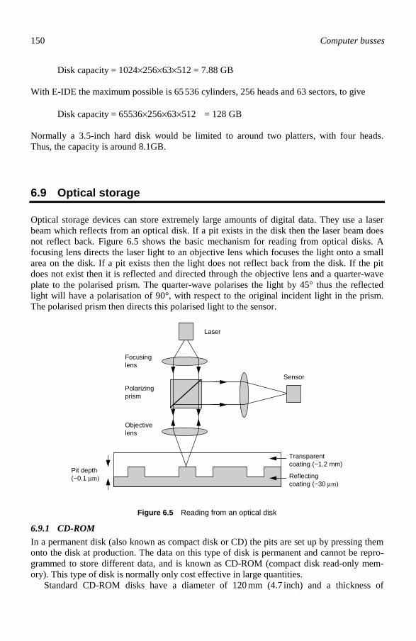
150 Computer busses
Disk capacity = 1024×256×63×512 = 7.88 GB With E-IDE the maximum possible is 65 536 cylinders, 256 heads and 63 sectors, to give Disk capacity = 65536×256×63×512 = 128 GB Normally a 3.5-inch hard disk would be limited to around two platters, with four heads. Thus, the capacity is around 8.1GB.
6.9 Optical storage
Optical storage devices can store extremely large amounts of digital data. They use a laser beam which reflects from an optical disk. If a pit exists in the disk then the laser beam does not reflect back. Figure 6.5 shows the basic mechanism for reading from optical disks. A focusing lens directs the laser light to an objective lens which focuses the light onto a small area on the disk. If a pit exists then the light does not reflect back from the disk. If the pit does not exist then it is reflected and directed through the objective lens and a quarter-wave plate to the polarised prism. The quarter-wave polarises the light by 45° thus the reflected light will have a polarisation of 90°, with respect to the original incident light in the prism. The polarised prism then directs this polarised light to the sensor.
Sensor
Laser
Focusinglens
Objectivelens
Polarizingprism
Reflectingcoating (~30 µm)
Transparentcoating (~1.2 mm)
Pit depth(~0.1 µm)
Figure 6.5 Reading from an optical disk
6.9.1 CD-ROM In a permanent disk (also known as compact disk or CD) the pits are set up by pressing them onto the disk at production. The data on this type of disk is permanent and cannot be repro-grammed to store different data, and is known as CD-ROM (compact disk read-only mem-ory). This type of disk is normally only cost effective in large quantities. Standard CD-ROM disks have a diameter of 120 mm (4.7 inch) and a thickness of

IDE and mass storage 151
1.2 mm. They can store up to 650 MB of data which gives around 74 minutes of compressed video (MPEG format with near VCR quality) or uncompressed hi-fi audio. The reflective coating (normally aluminium) on the disk is approximately 30 µm and the pits are approxi-mately 0.1 µm long and deep. A protective transparent coating is applied on top of the reflec-tive coating with a depth of 1.2 mm (the approximate thickness of the disk). The protective coating also helps to focus the light beam from about 0.7 mm on the surface of the coating to the 0.1 µm pit. Data is stored on the disk as a spiral starting from the inside and ending at the outside (which is opposite to hard disk. The thickness of the track is 1.6 µm, which gives a total spiral length of 5.7 km.
6.9.2 WORM drives WORM (write once read many) disks allow data to be written to the optical disk once. The data is then permanent and thus cannot be altered. They are typically used in data logging applications and in making small volumes of CD-ROMs. A 350 mm (14inch) WORM disk can store up to 10GBs of data (5GB per side). This gives around 15 hours of compressed video (MPEG format with near VCR quality). WORM disks consist of two pieces of transparent material (normally glass) with a layer of metal (typically tellurium) sandwiched in between. Initially the metal recording surface is clear. A high intensity laser beam then writes information to the disk by burning small pits into the surface.
6.9.3 CD-R and CD-RW disks CD-R (CD-recordable) disks are write-once disks that can store up to 650 MB of data or 74 minutes of audio. For a disk to be read by any CD-ROM drive they must comply with ISO 9660 format. A CD-R disk can also be made multisession where a new file system is written each time the disk is written to. Unfortunately, this takes up around 14 MB of header data for each session. Typical parameters for sessions are:
No. of sessions Header information Data for each session 1 approx. 14MB 636MB one session 5 approx. 70MB 116MB each session 10 approx. 140MB 51MB each session 30 approx. 420MB 7.7MB each session Typically CD recorders write at two (or even four) times the standard writing/playback speed of 150 KB (75 sectors) per second. A CD-RW (CD-rewriteable) disk allows a disk to be written-to many times, but the file format is incompatible with standard CD-ROM systems (IS0 9660). The formatting of the CD-RW disk (which can take a few hours) takes up about 157 MB of disk space, which only leaves about 493 MB for data. New CD-R and CD-RW writing systems incorporate a smart laser system that eradicates the problem of dirt on the disk. It does this by adjusting the write power of the laser using Automatic Power Control. This allows the unit to continue to write when it encounters minor media errors such as dirt, smudges, small scratches, and so on.
6.9.4 CD-ROM disk format
The two main standards for writing a CD-ROM are ISO 9660 and UDF (universal disk for-mat). The ISO 9660 disk unfortunately uses 14 MB for each write to the disk. In 1980, Philips NV and Sony Corporation first announced the CD-DA (digital audio)

152 Computer busses
and in 1983 released the standard for CD-ROM. Then in 1988, they released the Red Book standard for recordable CD audio disks (CD-DA) This served as a blueprint for the Yellow Book specification for CD-ROMs (CD-ROM and CD-ROM-XA data format) and the Orange Book Parts 1 and 2 specifications for CD-Recordable (CD-R/CD-E (CD-recordable/CD-erasable)). In the Red Book standard a disk is organized into a number of segments: • Lead in – contains the table of contents for the disk that specifies the physical location of
each track. • Program area – contains the actual disk data or audio data and is divided up into 99
tracks, with a two-second gap between each track. • Lead out – contains a string of zeros which is a legacy of the old Red Book standard.
These zeros enabled old CD players to identify the end of a CD. The CD is laid out in a number of sectors. Each of these sectors contains 2352 bytes, made up of 2048 bytes of data and other information such as headers, sub-headers, error detection codes and so on. The data is organised into logical blocks. After each session a logical block has a logical address, which is used by the drive to find a particular logical block number (LBN). Within the tracks the CD can contain either audio or computer data. The most common formats for computer data are ISO 9660, hierarchical file system (HFS) and the Joliet file system. The ISO 9660 was developed at a time when disks required to be mass replicated. It thus wrote the complete file system at the time of creation, as there was no need for incremental creation. Now, with CD-R technology, it is possible to incrementally write to a disk. This is described as multisession. Unfortunately, after each session a new lead in and lead out must be written (requiring a minimum of 13 MB of disk space). This consists of: • 13.2 MB for the lead out for the first session and 4.4 MB for each subsequent session. • 8.8 MB for lead in for each session comprising 8.8 MB. Thus multisession is useful for writing large amounts of data for each session, but is not effi-cient when writing many small updates. Most new CD-R systems now use a track-at-once technique which stores the data one track at a time and only writes the lead in and lead out data when the session is actually finished. In this technique the CD can be built up with data over a long period of time. Unfortunately the disk cannot be read by standard CD-ROM drives until the session is closed (and written with the ISO 9660 format). Another disadvan-tage is that the Red Book only specifies up to 99 tracks for each CD. Unfortunately the ISO 9660 is not well-suited for packet writing and is likely to be phased out over the coming years.
6.9.5 Magneto-optical (MO) disks
As with CD-R disks, magneto-optical (MO) disks allow the data to be rewritten many times. These disks use magnetic and optical fields to store the data. Unfortunately the disk must first be totally erased before data is written (although new developments are overcoming this limitation).
6.9.6 Transfer rates
Optical disks spin at variable speeds, they spin at a lower rate on the outside of the disk than

IDE and mass storage 153
on the inside. Thus the disk increases its speed progressively as the data is read from the disk. The actual rate at which the drive reads the data is constant for the disk. The basic transfer rate for a typical CD-ROM is 150 KB/s. This has recently been increased to 300 KB/s (×2 CD drives), 600 KB/s (×4), 900 KB/s (×6), 1.5 MB/s (×10) and even 6 MB/s (×40).
6.9.7 Standards
Data disks are described in the following standards books, each of them specific to an area or type of data application. These books can be obtained by becoming a licensed CD developer with Philips. These standards apply to media, hardware, operating systems, file systems and software. Red Book World standard for all compact disks (CD-DA) (audio). Yellow Book Covers CD-ROM and CD-ROM-XA data formats. Green Book Covers CD-I data formats and operating systems (photo). White Book CD-I (video) Orange Book Covers CD-R/CD-E (CD-Recordable/CD-Eraseable). Blue Book CD-Enhanced (CD Extra, CD Plus).
6.9.8 Silver, green, blue or gold
CD-ROMs are available in a number of colours, these are: • Silver. These are read-only disks which are a stamped as an original disk. • Gold. These are recordable disks which use a basic phthalocyanine formulation which
was patented by Mitsui Toatsu Chemicals (MTC) of Japan, and is licensed to other phthalocyanine media manufacturers. They generally work better with 2m writing speeds as some models of disk can not be written to at 1m writing speed.
• Green. These are recordable disks which are based on cyanine-based formulations. They are not covered by a governing patent, and are more or less unique to the individual manufacturers. An early problem was encountered with cyanine-based disk as the dye became chemically unstable in the presence of sunlight. Other problems included a wide variation in electrical performance depending on write speed and location (inner or outer portion of the disk). Eventually, in 1995, some stabilising compounds were added. The best attempt produced a metal-stabilised cyanine dye formulation that gave excellent overall performance. Gradually the performance of these disks is approaching gold disk performance.
• Blue. These are recordable disks which are based on an azo media. This was designed and manufactured by Mitsubishi Chemical Corporation (MCC) and marketed through its US subsidiary, Verbatim Corporation.
6.10 Magnetic tape
Magnetic tapes use a thin plastic tape with a magnetic coating (normally of ferric oxide). Most modern tapes are either reel-to-reel or cartridge type. A reel-to-reel tape normally has two interconnected reels of tape with tension arms (similar to standard compact audio cas-settes). The cartridge type has a drive belt to spin the reels, this mechanism reduces the strain

154 Computer busses
on the tape and allows faster access speeds. Magnetic tapes have an extremely high capacity and are relatively cheap. Data is saved in a serial manner with one bit (or one record) at a time. This has the disadvantage that they are relatively slow when moving back and forward within the tape to find the required data. Typically, it may take many seconds (or even minutes) to search from the start to the end of a tape. In most applications, magnetic tapes are used to back up a system. This type of applica-tion requires large amounts of data to be stored reliably over time but the recall speed is not important. The most common types of tape are: • Reel-to-reel tapes – the tapes have two interconnected reels with an interconnecting tape
which is tensioned by tension arms. They were used extensively in the past to store com-puter-type data but have been replaced by the following three types (8 mm, QIC and DAT tapes).
• 8 mm video cartridge tapes – this type of tape was developed to be used in video cameras and is extremely compact. As with videotapes the tape wraps round the read/write head in a helix.
• Quarter inch cartridge (QIC) tapes – a QIC is available in two main sizes: 5.25 inch and 3.5 inch. They give capacities of 40 MB to tens of GB.
• Digital audio tapes (DAT) – this type of tape was developed to be used in hi-fi applica-tions and is extremely compact. As with the 8 mm tape, the tape wraps round the read/write head in a helix. The tape itself is 4 mm wide and can store several GBs of data with a transfer rate of several hundred kbps.
6.10.1 QIC tapes
QIC tapes are available in two sizes: 5.25 -inch and 3.5 -inch. The tape length ranges from 200 to 1000 feet, with a tape width of 0.25 -inch. Typical capacities range from 40 MB to tens of GB. A single capstan drive is driven by the tape drive. Figure 6.6 illustrates a QIC tape.
Drive belt
Capstandrive
Accessdoor
Figure 6.6 QIC tape
6.10.2 8 mm video tape
The 8 mm video tape is a high specification tape and was originally used in video cameras. These types are also known as Exabyte after the company that originally developed a back up system using 8 mm videotapes. They can be used to store several GBs of data with a transfer rate of 500 kbps. In order to achieve this high transfer rate the read/write head spins at 2000 rpm and the tape passes it at a relatively slow speed.

IDE and mass storage 155
6.11 Exercises
6.11.1 What is a typical data capacity for a CD-ROM disk: (a) 100 MB (b) 650 MB (c) 800 MB (d) 1 GB 6.11.2 Which interface is most often used in PCs to connect to hard-disk drives: (a) ST-506 (b) ISA (c) EISA (d) IDE 6.11.3 Which bus does the IDE share many of its signals with: (a) ST-506 (b) ISA (c) EISA (d) PCI 6.11.4 How many devices can a single IDE bus support: (a) 1 (b) 2 (c) 4 (d) 7 6.11.5 What is the base address for the primary IDE controller: (a) 1F0h (b) 170h (c) 2F0h (d) 270h 6.11.6 What is the base address for the secondary IDE controller: (a) 1F0h (b) 170h (c) 2F0h (d) 270h 6.11.7 What is the main advantage of E-IDE over IDE: (a) It is compatible with more hard-disk drives (b) It allows for larger hard-disk capacities (c) It is easier to interface to (d) It has a large data bus size 6.11.8 What is the main advantage, apart from increased transfer rate, that IDE has over
older interface standards, such as ST-506 and ESDI? 6.11.9 Explain how IDE differs from E-IDE and how E-IDE supports larger disk capaci-
ties. How does E-IDE use modes to define the maximum transfer rate. Which mode is the fastest?
6.11.10 Show that the maximum capacity of IDE is 528 MB and that the maximum capac-
ity (per disk) is 8.4 GB for E-IDE.

156 Computer busses
6.11.11 Which IRQ does an IDE connected disk drive normally use and what is the size of its data bus.
6.11.12 A floppy disk ribbon cable has a cable twist to differentiate between the A: drive
and the B: drive. How does the ribbon cable that connects two IDE connected drives differ. In addition, how many wires does the ribbon cable have.
6.11.13 Outline how three hard disks and a CD-ROM can be connected to the IDE bus.
What settings are required for the disks to connect properly? Which signal line differentiates between a master and a slave?
6.11.14 How are I/O addresses used to communicate with hard disks. How is data trans-
ferred to and from the disk? What are the standard address ranges for the primary and the secondary? If possible, check these on an available PC.
6.11.15 Which register is used to identify a hard disk error. Explain its operation. 6.11.16 Which is the IDE signal line that identifies if a slave device exists? 6.11.17 Prove that, 16-bit, 44.1 kHz sampled, stereo audio gives over 65 minutes for a
650 MB optical disk.
6.12 Notes from the author
The IDE bus. What can you say about it? Not much really. It has no future plans for glory and is looking forward to a graceful retirement. It works, it’s reliable, it’s standard, it’s cheap, blah, blah, and relatively easy to set up. I’ve spent many a happy hour (not!) setting the jumpers on CD-ROM drives and secondary hard-disk drives which I want to add to a PC system. Luckily, these days, modern disk drives and BIOS cope well with adding and deleting disk drives to systems. On its negative side, IDE is not really that fast, but it really doesn’t have to be, as disk drives do not require high data rates. E-IDE improved IDE a great deal and only required a simple change in the BIOS. In conclusion, SCSI is the natural choice for disk drives and al-lows for much greater flexibility in configuration and also high data rates. But, it tends to be more expensive, and we’d miss IDE, wouldn’t we? In Chapter 3, I voted the IDE bus as the third most helpful bus of all-time. It merited this position as, over the years, it has quietly interfaced to disk drives, and has even supported the addition of CD-ROM drives. By the flick of a BIOS chip, it supported large capacity disk drives (EIDE). It also requires very little to set it up, as the BIOS tends is able to determine the capacity of the disk drive, and properly set it up. At present, there are no real plans to phase the IDE out, thus it is likely to stay a standard part of the motherboard. Unix workstations and Apple computers have always used the SCSI bus, as it gives easy external disk upgrades, but, as few users of PC require to add external disk drives to their computer, there has never really been a great demand for SCSI-based disk drives for the PC. IDE drives have two interrupts lines set aside for themselves, so why not use them to inter-face to disk drives. The SCSI bus, though, now offers high data rates, improved connectivity, improved command and message structure, and easy-of-upgrade. So why isn’t it the stan-dard bus for PC system. Well it costs more, doesn’t it, and well, it isn’t PC, is it? It’s an Ap-ple thing, isn’t it. When has the PC ever done anything in the right way?

SCSI
7.1 Introduction
SCSI has many advantages over IDE, these include: • A single bus system for up to seven connected devices. • It supports many different peripherals, such as hard disks, tape drives, CD-ROMs, and so
on. • It supports device priority where a higher SCSI-ID has priority over a lower SCSI-ID. • It supports both high-quality connectors and cables, and low-quality connection and rib-
bon cable. • It supports differential signals, which gives longer cable lengths. • Extended support for commands and messaging. • Devices do not need individual IRQ lines (as they do in IDE) as the controller communi-
cates with the devices. • It has great potential for faster transfer and enhanced peripheral support.
7.2 SCSI types
SCSI has an intelligent bus subsystem and can support multiple devices cooperating cur-rently. Each device is assigned a priority. The main types of SCSI are: • SCSI-I. Transfer rate of 5 MB/s with an 8-bit data bus and seven devices per controller. • SCSI-II. Support for SCSI-1 and with one or more of the following:
• Fast SCSI which uses a synchronous transfer to give 10 MB/s transfer rate. The initia-tor and target initially negotiate to see if they can both support synchronous transfer. If they can they then go into a synchronous transfer mode.
• Fast/wide SCSI-2 which doubles the data bus width to 16 bits to give 20 MB/s trans-fer rate.
• 15 devices per master device. • Tagged command queuing (TCQ) which greatly improves performance and is sup-
ported by Windows NT, NetWare and OS/2. • Multiple commands sent to each device. • Commands executed in whatever sequence will maximize device performance.
• Ultra SCSI (SCSI-III). Operates either as 8-bit or 16-bit with either 20 MB/s or 40 MB/s transfer rate.
7

158 Computer busses
7.2.1 SCSI-II
SCSI-II supports fast SCSI which is basically SCSI-I operating at a rate of 10 MB/s (using synchronous versus asynchronous) and Wide SCSI which uses a 64-pin connector and a 16-bit data bus. The SCSI-II controller is also more efficient and processes commands up to seven times faster than SCSI-I. The SCSI-II drive latency is also much less than SCSI-I due mainly to tag command queuing (TCQ) which allows multiple commands to be sent to each device. Each device then holds its own commands and executes them in whatever sequence that will maximize per-formance (such as by minimizing the latency associated with disk rotation). Table 7.1 con-trasts Fast SCSI-II and Fast/Wide SCSI-II. It can be seen that both disks have predictive fail-ure analysis (PFA) and automatic defect reallocation (ADR). The normal 50-core cable is typically known as A-cable, while the 68-core cable is known as B-cable.
Table 7.1 Comparison of SCSI-II disks
Seek time (ms)
Latency (ms)
Rotational speed (rpm)
Sustained data read (MB/s)
PFA ADR
1 GB SCSI-II fast 10.5 5.56 5400 4
4.5 GB SCSI-II fast/ wide 8.2 4.17 7200 12
7.2.2 Ultra SCSI
Ultra SCSI (or SCSI-III) allows for 20 MB/s burst transfers on an 8-bit data path and 40 MB/s burst transfer on a 16-bit data path. It uses the same cables as SCSI-II and the maxi-mum cable length is 1.5 m. Ultra SCSI disks are compatible with SCSI-2 controllers; how-ever the transfer will be at the slower speed of the SCSI controller. SCSI disks are compati-ble with UltraSCSI controllers; however, the transfer will be at the slower speed of the SCSI disk. SCSI-I and Fast SCSI-II use a 50-pin 8-bit connector, whereas fast/wide SCSI-II and Ul-tra SCSI uses a 68-pin 16-bit connector. The 16-bit connector is physically smaller than the 8-bit connector and the 16-bit connector cannot connect directly to the 8-bit connector. The cable used is called P-cable and replaces the A/B-cable. Note that SCSI-II, and Ultra SCSI require an active terminator on the last external device. Table 7.2 compares the main types of SCSI.
Table 7.2 SCSI types
Data bus (bits)
Transfer rate (MB/s)
Tagged command queuing
Parity checking
Maximum devices
Pins on cable and connector
SCSI-I 8 5 × ×/ (optional) 7 50 SCSI-II Fast 8 10 (10MHz) 7 50 SCSI-II fast/ wide
16 20 (10MHz) 15 68
Ultra SCSI 16 40 (20MHz) 15 68

SCSI 159
7.3 SCSI interface
In its standard form the small computer systems interface (SCSI) standard uses a 50-pin header connector and a ribbon cable to connect to up to eight devices. It overcomes the prob-lems of the IDE, where devices have to be assigned as a master and a slave. SCSI and fast SCSI transfer one byte at a time with a parity check on each byte. SCSI-II, wide SCSI and Ultra SCSI use a 16-bit data transfer and a 68-pin connector. Table 7.3 lists the pin connec-tions for SCSI-I (single-ended cable) and Fast SCSI (differential cable) and Table 7.4 lists the pin connections for SCSI-II, wide SCSI and ultra SCSI.
Table 7.3 SCSI-I and Fast SCSI connections
Single-ended cable Differential cable Pin Signal Pin Signal Pin Signal Pin Signal 1 GND 2 D0 1 GND 2 GND 3 GND 4 D1 3 + D0 4 – D0 5 GND 6 D2 5 + D1 6 – D1 7 GND 8 D3 6 + D2 8 – D2 9 GND 10 D4 8 + D3 10 – D3 11 GND 12 D5 11 + D4 12 – D4 13 GND 14 D6 13 + D5 14 – D5 15 GND 16 D7 15 + D6 16 – D6 17 GND 18 D(PARITY) 17 + D7 18 – D7 19 GND 20 GND 19 D(PARITY) 20 – D(PARITY) 21 GND 22 GND 21 DIFFSEN 22 GND 23 RESERVED 24 RESERVED 23 RESERVED 24 RESERVED 25 Open 26 TERMPWR 25 TERMPWR 26 TEMPWR 27 RESERVED 28 RESERVED 27 RESERVED 28 RESERVED 29 GND 30 GND 29 + ATN 30 – ATN 31 GND 32 ATN 31 GND 32 GND 33 GND 34 GND 33 + RST 34 – RST 35 GND 36 BSY 35 + ACK 36 – ACK 37 GND 38 ACK 37 + RST 38 – RST 39 GND 40 RST 39 + MSG 40 – MSG 41 GND 42 MSG 41 + SEL 42 – SEL 43 GND 44 SEL 43 + C / D 44 – C / D 45 GND 46 C / D 45 + REQ 46 – REQ 47 GND 48 REQ 47 + I / O 48 – I / O 49 GND 50 I / O 49 GND 50 GND
7.3.1 Signals
A SCSI bus is made up of a SCSI host adapter connected to a number of SCSI units via a SCSI bus. As all units connect to a common bus, only two units can transfer data at a time, either from one SCSI unit to another or from one SCSI unit to the SCSI host. The great ad-vantage of this transfer is that is does not involve the processor.

160 Computer busses
Table 7.4 SCSI-II, wide SCSI and ultra SCSI
Pin Signal Pin Signal 1 GND 35 GND 2 GND 36 D8 3 GND 37 D9 4 GND 38 D10 5 GND 39 D11 6 GND 40 D12 7 GND 41 D13 8 GND 42 D14 9 GND 43 D15 10 GND 44 D(PARITY1) 11 GND 45 ACKB 12 GND 46 GND 13 GND 47 REQB 14 GND 48 D16 15 GND 49 D17 16 GND 50 D18 17 TERMPWR 51 TERMPWR 18 TERMPWR 52 TERMPWR 19 GND 53 D19 20 GND 54 D20 21 GND 55 D21 22 GND 56 D22 23 GND 57 D23 24 GND 58 D(PARITY2) 25 GND 59 D24 26 GND 60 D25 27 GND 61 D26 28 GND 62 D27 29 GND 63 D28 30 GND 64 D29 31 GND 65 D30 32 GND 66 D31 33 GND 67 D(PARITY3) 34 GND 68 GND
Each unit on a SCSI is assigned a SCSI ID address. In the case of SCSI-I this ranges from 0 to 7 (where 7 is normally reserved for a tape drive). The host adapter takes one of the ad-dresses thus a maximum of seven units can connect to the bus. Most systems allow the units to take on any SCSI ID address, but older systems required boot drives to be connected to a specific SCSI address. When the system is initially booted, the host adapter sends out a Start Unit command to each SCSI unit. This allows each of the units to start in an orderly manner (and not overloading the local power supply). The host will start with the highest priority address (ID=7) and finishes with the lowest address (ID=0). Typically, the ID is set with a rotating switch selector or by three jumpers. SCSI defines an initiator control and a target control. The initiator requests a function from a target, which then executes the function, as illustrated in Figure 7.1. The initiator ef-

SCSI 161
fectively takes over the bus for the time to send a command and the target executes the com-mand and then contacts the initiator and transfers any data. The bus will then be free for other transfers. The main signals are: • BSY – indicates that the bus is busy, or not (an OR-tied signal). • ACK – activated by the initiator to indicate an acknowledgement for a REQ information
transfer handshake. • RST – when active (low) resets all the SCSI devices (an OR-tied signal). • ATN – activated by the initiator to indicate the attention state. • MSG – activated by the target to indicate the message phase. • SEL – activated by the initiator and is used to select a particular target device (an OR-tied
signal). • C / D (control/data) – activated by the target to identify if there is data or control on the
SCSI bus. • REQ – activated by the target to acknowledge to indicate a request for an ACK informa-
tion transfer handshake. • I / O (input/output) – activated by the target to show the direction of the data on the data
bus. Input defines that data is an input to the initiator, else it is an output. Each of the control signals can be true or false. They can be: • OR-tied driven, where the driver does not drive the signal to the false state. In this case
the bias circuitry of the bus terminators pulls the signal false whenever it is released by the drivers at every SCSI device. If any driver is asserted, then the signal is true. The BSY , SEL , and RST signals are OR-tied. In the ordinary operation of the bus, the BSY and RST signals may be simultaneously driven true by several drivers.
• Non-OR-tied driven, where the signal may be actively driven false. No signals other than BSY , RST and D(PARITY) are simultaneously driven by two or more drivers.
Initiator Target
Functionrequest
Functionexecutor
SCSI bus
Figure 7.1 Initiator and target in SCSI

162 Computer busses
7.4 SCSI operation
The SCSI bus allows any unit to talk to any other unit, or the host to talk to any unit. Thus there must be some way of arbitration where units capture the bus. The main phases that the bus goes through are: • Free-bus. In this state there are no units which either transfer data or have control of the
bus. It is identified by disactive SEL and BSY (both will be high). Thus, any unit can cap-ture the bus.
• Arbitration. In this state a unit can take control of the bus and become an initiator. To do this it activates the BSY signal and puts its own ID address on the data bus. Next, after a delay, it tests the data bus to determine if a high-priority unit has put its own address on the bus. If it has then it will allow the other unit access to the bus. If its address is still on the bus then it asserts the SEL line. After a delay, it then has control of the bus.
• Selection. In this state the initiator selects a target unit and gets the target to carry out a given function, such as reading or writing data. The initiator outputs the OR value of its SCSI-ID and the SCSI-ID of the target onto the data bus (for example, if the initiator is 2 and the target is 5 then the OR-ed ID on the bus will be 00100100.). The target then de-termines that its ID is on the data bus and set the BSY line active. If this does not happen within a given time then the initiator deactivates the SEL signal, and the bus will be free. The target determines that it is selected when the SEL signal and its SCSI ID bit are ac-tive and the BSY and I / O signals are false. It then asserts the BSY signal within a selec-tion abort time.
• Reselection. When the arbitration phase is complete, the winning SCSI device asserts the BSY and SEL signals and has delayed at least a bus clear delay plus a bus settle delay. The winning SCSI device sets the DATA BUS to a value that is the logical OR of its SCSI ID bit and the initiator’s SCSI ID bit. Sometimes the target takes some time to reply to the initiators request. The initiator determines that it is reselected when the SEL and I / O signals and its SCSI ID bit are true and the BSY signal is false. The reselected initia-tor then asserts the BSY signal within a selection abort time of its most recent detection of being reselected. An initiator does not respond to a reselection phase if other than two SCSI ID bits are on the data bus. After the target detects that the BSY signal is true, it also asserts the BSY signal and waits a given time delay and then releases the SEL signal. The target may then change the I / O signal and the data bus. After the reselected initiator detects the SEL signal is false, it releases the BSY signal. The target continues to assert the BSY signal until it gives up the SCSI bus.
• Command. The command phase is used by the target to request command information from the initiator. The target asserts the C / D signal and negates the I / O and MSG sig-nals during the REQ / ACK handshake(s) of this phase.
• Data. The data phase covers both the data in and data out phases. In the data in phase the target requests that data be sent to the initiator from the target. For this purpose the target asserts the I / O signal and negates the C / D and MSG signals during the REQ / ACK handshake(s) of this phase. In the data out phase, the target requests that data be sent from the initiator to the target. The target negates the C / D , I / O and MSG signals during the REQ / ACK handshake(s) of this phase.
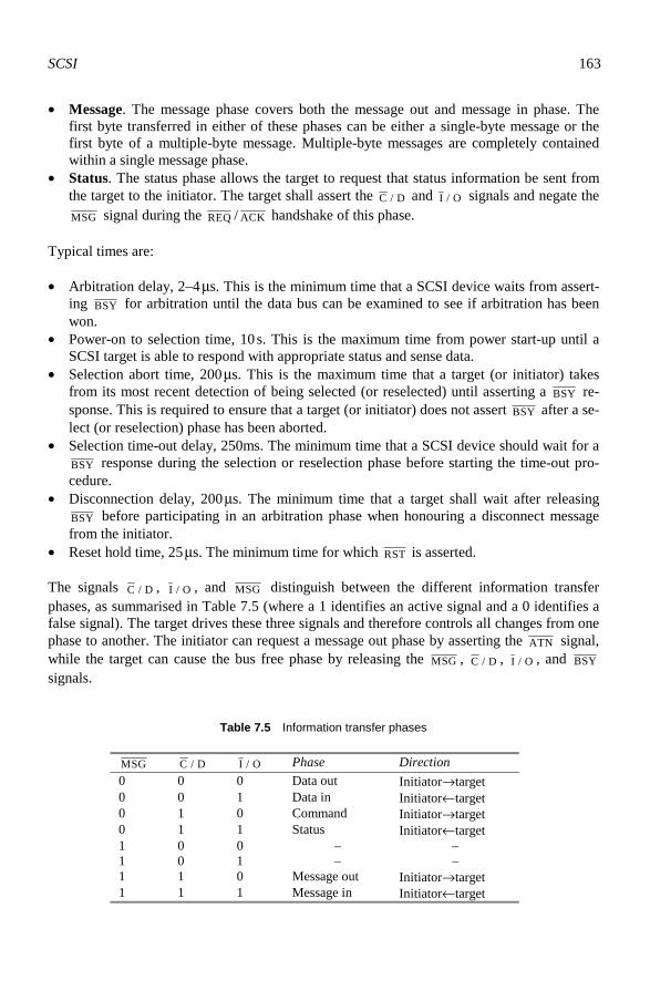
SCSI 163
• Message. The message phase covers both the message out and message in phase. The first byte transferred in either of these phases can be either a single-byte message or the first byte of a multiple-byte message. Multiple-byte messages are completely contained within a single message phase.
• Status. The status phase allows the target to request that status information be sent from the target to the initiator. The target shall assert the C / D and I / O signals and negate the MSG signal during the REQ / ACK handshake of this phase.
Typical times are: • Arbitration delay, 2–4 µs. This is the minimum time that a SCSI device waits from assert-
ing BSY for arbitration until the data bus can be examined to see if arbitration has been won.
• Power-on to selection time, 10 s. This is the maximum time from power start-up until a SCSI target is able to respond with appropriate status and sense data.
• Selection abort time, 200 µs. This is the maximum time that a target (or initiator) takes from its most recent detection of being selected (or reselected) until asserting a BSY re-sponse. This is required to ensure that a target (or initiator) does not assert BSY after a se-lect (or reselection) phase has been aborted.
• Selection time-out delay, 250ms. The minimum time that a SCSI device should wait for a BSY response during the selection or reselection phase before starting the time-out pro-cedure.
• Disconnection delay, 200µs. The minimum time that a target shall wait after releasing BSY before participating in an arbitration phase when honouring a disconnect message from the initiator.
• Reset hold time, 25µs. The minimum time for which RST is asserted. The signals C / D , I / O , and MSG distinguish between the different information transfer phases, as summarised in Table 7.5 (where a 1 identifies an active signal and a 0 identifies a false signal). The target drives these three signals and therefore controls all changes from one phase to another. The initiator can request a message out phase by asserting the ATN signal, while the target can cause the bus free phase by releasing the MSG , C / D , I / O , and BSY signals.
Table 7.5 Information transfer phases
MSG C / D I / O Phase Direction 0 0 0 Data out Initiator→target 0 0 1 Data in Initiator←target 0 1 0 Command Initiator→target 0 1 1 Status Initiator←target 1 0 0 – – 1 0 1 – – 1 1 0 Message out Initiator→target 1 1 1 Message in Initiator←target

164 Computer busses
The information transfer phases use one or more REQ / ACK handshakes to control the infor-mation transfer. Each REQ / ACK handshake allows the transfer of one byte of information. During the information transfer phases the BSY signal shall remain true and the SEL signal shall remain false. Additionally, during the information transfer phases, the target shall con-tinuously envelope the REQ / ACK handshake(s) with the C / D , I / O and MSG signals in such a manner that these control signals are valid for a bus settle delay before the assertion of the REQ signal of the first handshake and remain valid until after the negation of the ACK signal at the end of the handshake of the last transfer of the phase. The I / O signal allows the target to control the direction of information, when its I / O signal is true then the information is transferred from the target to the initiator and when false, the transfer is from the initiator to the target. The handshaking operation for a transfer to the initiator is as follows: • The I / O signal is asserted as a true. • The target sets the data bus lines. • The target asserts the REQ signal. • The initiator reads the data bus. • The initiator then indicates its acceptance of the data by asserting the ACK signal. • The target may change or release the data bus. • The target negates the REQ signal. • The initiator shall then negate the ACK signal. • The target may continue the transfer by driving the data bus and asserting the REQ signal,
and so on. The handshaking operation for a transfer from the initiator is as follows: • The I / O signal is asserted as a false. • The target asserts the REQ signal (requesting information). • The initiator sets the data bus lines. • The initiator asserts the ACK signal. • The target then reads the data bus. • The target negates the REQ signal (acknowledging transfer). • The initiator may then set the data bus, and so on.
7.5 SCSI pointers
SCSI provides for three pointers for each I/O process (called saved pointers), for command, data and status. When an I/O process becomes active, its three saved pointers are copied into the initiator’s set of three current pointers. These current pointers point to the next command, data or status byte to be transferred between the initiator’s memory and the target.

SCSI 165
7.6 Message system description
The message system allows the initiator and the target to communicate over the interface connection. Each message can be one, two, or multiple bytes in length. In a single message phase, one or more messages can be transmitted, (but a message cannot be split between multiple message phases). Table 7.6 lists the message format, where the first byte of the mes-sage determines the format. The initiator ends the message out phase (by negating ATN ) when it sends certain messages identified in Table 7.7. Single-byte messages consist of a single byte transferred during a message phase. Table 7.7 defines the message type.
Table 7.6 Message format
Value Message format 00h One byte message (command complete) 01h Extended messages 02h–1Fh One-byte messages 20h–2Fh Two-byte messages 30h–7Fh Reserved 80h–FFh One-byte message (identify)
Table 7.7 Message codes
Code Message Direction Description 00h Command complete In Sent from a target to an initiator to indicate that
the execution of an I/O process has completed and that valid status has been sent to the initia-tor. After successfully sending this message, the target shall go to the bus free phase by re-leasing the BSY signal. The target considers the message transmission to be successful when it detects the negation of ACK for the com-mand complete message with the ATN signal false.
03h Restore pointers
In
04h Disconnect In/Out Sent from a target to inform an initiator that the present connection is going to be broken (the target plans to disconnect by releasing the BSY signal), but that a later reconnect will be re-quired in order to complete the current I/O process. This message shall not cause the initia-tor to save the data pointer. After successfully sending this message, the target shall go to the bus free phase by releasing the BSY signal. The target shall consider the message transmis-sion to be successful when it detects the nega-tion of the ACK signal for the disconnect mes-sage with the ATN signal false.

166 Computer busses
05h Initiator-detected error
Out
06h Abort Out Sent from the initiator to the target to clear any I/O process. The target goes to the bus-free phase following successful receipt of this mes-sage.
07h Message reject Out Sent from either the initiator or target to indi-cate that the last message or message byte it received was inappropriate or has not been implemented.
08h No operation Out Sent from an initiator in response to a target’s request for a message when the initiator does not currently have any other valid message to send.
09h Message parity error Out
0Ah Linked command complete
In
0Bh Linked command complete (with flag)
In
0Ch Bus device reset Out Sent from an initiator to direct a target to clear all I/O processes on that SCSI device. This message forces a hard reset condition to the selected SCSI device.
0Dh Abort tag Out
0Eh Clear queue Out
0Fh Initiate recovery In/Out
10h Release recovery Out
11h Terminate I/O process
Out
12h–1Fh
Reserved
23h Ignore wide residue (2 bytes)
24h–2Fh Reserved for two-byte messages
30h–7Fh
Reserved
80h–FFh Identify In/Out

SCSI 167
7.7 SCSI commands
A command is sent from the initiator to the target. The first byte of all SCSI commands con-tains an operation code, followed by a command descriptor block and finally the control byte. The format of the command descriptor block for 6-byte commands is: • Byte 0 – operation code. • Byte 1 – logical unit number (MSB, if required). • Byte 2 – logical bock address. • Byte 3 – logical bock address (LSB, if required). • Byte 4 – transfer length (if required) / Parameter list length (if required) / allocation
length (if required). • Byte 5 – control.
7.7.1 Operation code
Figure 7.2 shows the operation code of the command descriptor block. It has a group code field and a command code field. The 3-bit group code field provides for eight groups of com-mand codes and the 5-bit command code field provides for 32 command codes in each group. The group code specifies one of the following groups: • Group 0 – 6-byte commands. • Group 1/2 – 10-byte commands. • Group ¾ – reserved. • Group 5 – 12-byte commands. • Group 6/7 – vendor-specific.
b7 b6 b5 b4 b3 b2 b1 b0
Command codeGroup code
Figure 7.2 Operation code
7.7.2 Logical unit number
The logical unit number (LUN) is defined in the identify message. The target ignores the LUN specified within the command descriptor block if an identify message was received (normally the logical unit number in the command descriptor block to be set to zero).
7.7.3 Logical block address
The logical block address (LBA) on logical units or within a partition on device volumes begins with block zero and is contiguous up to the last logical block on that logical unit or within that partition. A 10-byte and a 12-byte command descriptor blocks contain 32-bit logical block ad-dresses, whereas a 6-byte command descriptor block contains a 21-bit logical block address.
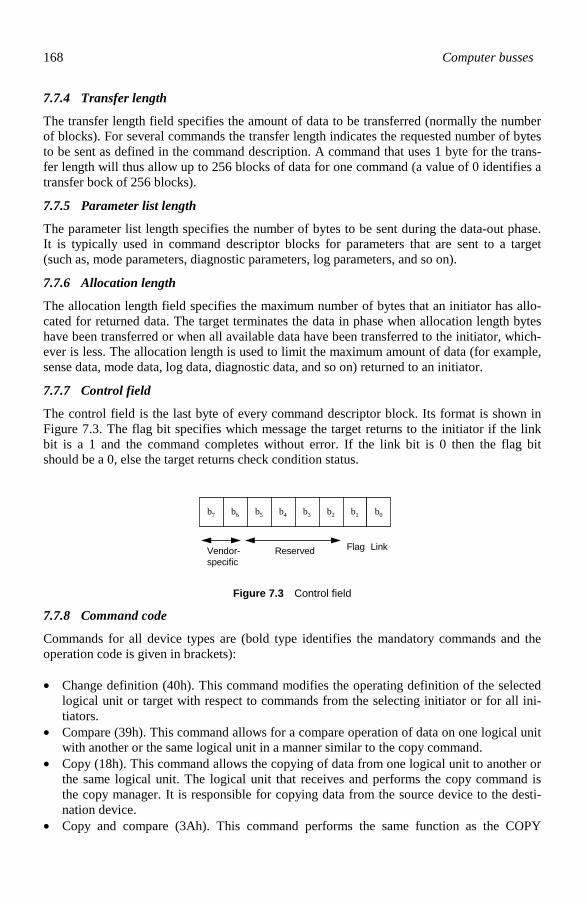
168 Computer busses
7.7.4 Transfer length
The transfer length field specifies the amount of data to be transferred (normally the number of blocks). For several commands the transfer length indicates the requested number of bytes to be sent as defined in the command description. A command that uses 1 byte for the trans-fer length will thus allow up to 256 blocks of data for one command (a value of 0 identifies a transfer bock of 256 blocks).
7.7.5 Parameter list length
The parameter list length specifies the number of bytes to be sent during the data-out phase. It is typically used in command descriptor blocks for parameters that are sent to a target (such as, mode parameters, diagnostic parameters, log parameters, and so on).
7.7.6 Allocation length
The allocation length field specifies the maximum number of bytes that an initiator has allo-cated for returned data. The target terminates the data in phase when allocation length bytes have been transferred or when all available data have been transferred to the initiator, which-ever is less. The allocation length is used to limit the maximum amount of data (for example, sense data, mode data, log data, diagnostic data, and so on) returned to an initiator.
7.7.7 Control field
The control field is the last byte of every command descriptor block. Its format is shown in Figure 7.3. The flag bit specifies which message the target returns to the initiator if the link bit is a 1 and the command completes without error. If the link bit is 0 then the flag bit should be a 0, else the target returns check condition status.
b7 b6 b5 b4 b3 b2 b1 b0
LinkFlagReservedVendor-specific
Figure 7.3 Control field
7.7.8 Command code
Commands for all device types are (bold type identifies the mandatory commands and the operation code is given in brackets): • Change definition (40h). This command modifies the operating definition of the selected
logical unit or target with respect to commands from the selecting initiator or for all ini-tiators.
• Compare (39h). This command allows for a compare operation of data on one logical unit with another or the same logical unit in a manner similar to the copy command.
• Copy (18h). This command allows the copying of data from one logical unit to another or the same logical unit. The logical unit that receives and performs the copy command is the copy manager. It is responsible for copying data from the source device to the desti-nation device.
• Copy and compare (3Ah). This command performs the same function as the COPY

SCSI 169
command, except that a verification of the data written to the destination logical unit is performed after the data is written.
• Inquiry (12h). This command requests that information regarding parameters of the target and its attached peripheral device(s) be sent to the initiator.
• Log select (4Ch). This command provides a means for the initiator to manage statistical information maintained by the device about the device or its logical units. Targets that implement the log select command shall also implement the log sense command. Struc-tures in the form of log parameters within log pages are defined as a way to manage the log data. The log select command provides for sending zero or more log pages during a data out phase.
• Log sense (4Dh). This command allows the initiator to retrieve statistical information maintained by the device about the device or its logical units. It is a complementary command to the log select command.
• Mode select (15h). This command provides a means for the initiator to specify medium, logical unit, or peripheral device parameters to the target. Targets that implement the mode select command shall also implement the mode sense command.
• Mode sense (1Ah). This command allows a target to report parameters to the initiator and is a complementary command to the mode select command.
• Read buffer (3Ch). This command is used in conjunction with the write buffer command as a diagnostic function for testing target memory and the SCSI bus integrity.
• Receive diagnostic results (1Ch). This command requests analysis data be sent to the ini-tiator after completion of a send diagnostic.
• Send diagnostic (1Dh). This command requests the target to perform diagnostic opera-tions on itself, on the logical unit, or on both.
• Test unit ready (00h). This command provides a means to check if the logical unit is ready. This is not a request for a self-test. If the logical unit would accept an appropriate medium-access command without returning check condition status, this command shall return a good status.
• Write buffer (3Bh). This command is used in conjunction with the read buffer command as a diagnostic for testing target memory and the SCSI bus integrity.
7.8 Status
The status phase normally occurs at the end of a command (although in some cases may oc-cur before transferring the command descriptor block). Figure 7.4 shows the format of the status byte and Table 7.8 defines the status byte codes. This status byte is sent from the target to the initiator during the status phase at the completion of each command unless the com-mand is terminated by one of the following events: • Abort message. • Abort tag message. • Bus device reset message. • Clear queue message. • Hard reset condition. • Unexpected disconnect.

170 Computer busses
b7 b6 b5 b4 b3 b2 b1 b0
ReservedStatus byte codeReserved
Figure 7.4 Status field
Table 7.8 Status byte codes
Bit values of status byte Status Description 7 6 5 4 3 2 1 0 R R 0 0 0 0 0 R Good Indicates that the target has successfully completed the
command.
R R 0 0 0 0 1 R Check condition
Indicates that a contingent allegiance condition has oc-curred.
R R 0 0 0 1 0 R Condition met This status or INTERMEDIATE-CONDITION MET is returned whenever the requested operation is satisfied.
R R 0 0 1 0 0 R Busy Indicates that the target is busy. This status shall be re-turned whenever a target is unable to accept a command from an otherwise acceptable initiator (that is, no reserva-tion conflicts).
R R 0 1 0 0 0 R Immediate This status or INTERMEDIATE-CONDITION MET shall be returned for every successfully completed com-mand in a series of linked commands (except the last command).
R R 0 1 0 1 0 R Immediate-condition met
This status is the combination of the CONDITION MET and INTERMEDIATE status’s.
R R 0 1 1 0 0 R Reservation conflict
This status occurs whenever an initiator attempts to ac-cess a logical unit that is reserved with a conflicting res-ervation type for another SCSI device.
R R 1 0 0 0 1 R Command conflict
This status occurs whenever the target terminates the current I/O process after receiving a TERMINATE I/O PROCESS message.
R R 1 0 1 0 0 R Queue full This status shall be implemented if tagged queuing is implemented.
R R R R R R R R Reserved

SCSI 171
7.9 Exercises
7.9.1 What is the maximum number of devices that can connect to a standard SCSI bus: (a) 1 (b) 4 (c) 7 (d) 8 7.9.2 How many data bits does the SCSI-I bus use: (a) 8 (b) 16 (c) 32 (d) 64 7.9.3 How many data bits does the SCSI-II fast/wide bus use: (a) 8 (b) 16 (c) 32 (d) 64 7.9.4 How is device priority implemented on the SCSI bus: (a) by active polling (b) by interrupt priority (c) by brute force (d) by unit IDs 7.9.5 What method does the SCSI bus use to prevent devices from hogging the bus: (a) Time-outs (b) Interrupts (c) Active polling (d) Memory mapping 7.9.6 The transfer clock for a SCSI bus is 20 MHz. Which is the transfer rate for a 16-bit
data bus: (a) 10 MB/s (b) 20 MB/s (c) 40 MB/s (d) 80 MB/s 7.9.7 Explain the main differences between SCSI-I, SCSI-II and ultra SCSI. Outline
their maximum data throughput, the connectors used and the size of their data bus-ses. Also, outline some of the advantages of SCSI over busses such as the ISA bus.
7.9.8 State the SCSI lines that are used for simple error detection. Why is it not possible
to detect which bits are in error? 7.9.9 Discuss the main system lines that are used in the SCSI bus and the operation of
OR-tied driven signals. 7.9.10 Outline the main phases that the initiator and target go through in setting up a con-
nection. Also, outline the importance of device time-outs for the different SCSI phases.
172 Computer busses
7.9.11 Discuss how the MSG , C / D and I / O signals are used to set up different transfer phases.
7.9.12 Explain how SCSI uses the SCSI-ID address to set up a device priority system. 7.9.13 Discuss the usage of the message phase in SCSI and cite typical examples of its
usage. 7.9.14 Discuss the usage of the command phase in SCSI and cite typical examples of its
usage. 7.9.15 Discuss the usage of the status phase in SCSI and cite typical examples.
7.10 Notes from the author
Well I did it. I covered SCSI in a single chapter. It wasn’t easy, but its here. SCSI is a mas-sive area, and one which could fill this book three or four times over. So, as I do not have enough space for the full specification, I’ve tried to give a flavour of the bus. SCSI’s full grown-up name is the small computer systems interface. It is difficult to define exactly what a small computer system is1, but SCSI has outgrown its original application of interfacing to ‘small’ systems and to external disk drives. It now has the potential of being able to interface virtually any external peripheral to a system. It can also be used to connect devices internally within a system. Typically, it takes a bit longer to initially boot the system, but once it has, it should be as reliable as any non-SCSI device. An important concept in SCSI is the prioritisation of devices using SCSI IDs. Few busses allow the system to prioritise peripherals. Thus, in a properly configured system, fast devices which require to be quickly serviced will always get access onto the bus before slow devices which do not require fast servicing. Unfortunately, the method SCSI uses limits the number of devices to one less than the number of bits on the data bus (seven for an 8-bit data bus and 15 for a 16-bit data bus). In most cases, this is not a major problem. For example, two hard disks, two CD-ROM drives, a tape backup system, a zip drive and a midi keyboard could all be attached to a standard SCSI-I bus. In most PCs the IDE drive is still used in the majority of systems, as it is relatively easy to set up and its cheap. It is also dedicated to interfacing to the disk drives; thus, no other pe-ripheral can hog the disk drive bus. However, for most general-purpose applications, SCSI is best. New standards for SCSI give a 16-bit data bus, at a transfer rate of 20 MHz, giving a maximum data throughput of 40 MB/s, which is much faster than IDE. It is also much easier to configure a SCSI system than it is connecting peripherals internally in a PC. A SCSI sys-tem only requires a single interrupt line, for all the devices that are connected. Ask someone who has set up a Unix network, or who has configured an Apple computer, and they will tell you that there is little to beat a well set up SCSI bus. It’s reliable, and it is easy-to-upgrade.
1 Probably, ‘small computer’ means ‘not a mainframe computer’ or ‘a less powerful com-
puter’. One must remember that SCSI was developed at a time when mainframe com-puters were kings and PCs were seen as glorified typewriters.

PCMCIA
8.1 Introduction
The Personal Computer Memory Card International Association (PCMCIA) interface allows small thin cards to be plugged into laptop, notebook or palmtop computers. It was originally designed for memory cards (Version 1.0) but has since been adopted for many other types of adapters (Version 2.0), such as fax/modems, sound cards, local area network cards, CD-ROM controllers, digital I/O cards, and so on. Most PCMCIA cards comply with either PCMCIA Type II or Type III. Type I cards are 3.3 mm thick, Type II take cards up to 5 mm thick, Type III allows cards up to 10.5 mm thick. A new standard, Type IV, takes cards which are greater than 10.5 mm. Type II interfaces can accept Type I cards, Type III accept Types I and II and Type IV interfaces accept Types I, II and III. The PCMCIA standard uses a 16-bit data bus (D0–D15) and a 26-bit address bus (A0–A25), which gives an addressable memory of 226 bytes (64 MB). The memory is arranged as: • Common memory and attribute memory, which gives a total addressable memory of
128 MB. • I/O addressable space of 65 536 (64 k) 8-bit ports. The PCMCIA interface allows the PCMCIA device to map into the main memory or into the I/O address space. For example, a modem PCMCIA device would map its registers into the standard COM port addresses (such as 3F8h–3FFh for COM1 or 2F8h–2FF for COM2). Any accesses to the mapped memory area will be redirected to the PCMCIA rather that the main memory or I/O address space. These mapped areas are called windows. A window is defined with a START address and a LAST address. The PCMCIA control register contains these addresses.
8.2 PCMCIA signals
Table 8.1 shows the pin connections. The main PCMCIA signals are: • A25–A0, D15–D0 – data bus (D15–D0) and a 26-bit memory address (A25–A0) or 16-bit
I/O memory address (A15–A0). • 1 DETECT CARD , CARD DETECT 2 – used to detect if a card is present in a socket. When a
card is inserted one of these lines is pulled to a low level.
8

174 Computer busses
Table 8.1 PCMCIA connections
Pin Signal Pin Signal Pin Signal Pin Signal 1 GND 18 Vpp1 35 GND 52 Vpp2 2 D3 19 A16 36 See below 53 A22 3 D4 20 A15 37 D11 54 A23 4 D5 21 A12 38 D12 55 A24 5 D6 22 A7 39 D13 56 A25 6 D7 23 A6 40 D14 57 RFU 7 CARD ENABLE 1 24 A5 41 D15 58 RESET 8 A10 25 A4 42 See below 59 WAIT
9 OUTPUT ENABLE 26 A3 43 REFRESH 60 INPACK 10 A11 27 A2 44 IOR 61 REGISTER SELECT 11 A9 28 A1 45 IOW 62 SPKR 12 A8 29 A0 46 A17 63 STSCHG 13 A13 30 D0 47 A18 64 D8 14 A14 31 D1 48 A19 65 D9 15 See below 32 D2 49 A20 66 D10 16 BUSY/READY 33 IOIS16 50 A21 67 CARD DETECT 2 17 +5V 34 GND 51 +5V 68 GND
Pin 15 WRITE ENABLE / PROGRAM Pin 33 IOIS16 (Write Protect) Pin 36 CARD DETECT 1 Pin 42 2 ENABLE CARD • CARD ENABLE 1 , 2 ENABLE CARD – used to enable the upper 8-bits of the data bus
( CARD ENABLE 1 ) and/or the lower 8 bits of the data bus ( 2 ENABLE CARD ). • OUTPUT ENABLE – set low by the computer when reading data from the PCMCIA unit. • REGISTER SELECT – set high when accessing common memory or a low when accessing
attribute memory. • RESET – used to reset the PCMCIA card. • REFRESH – used to refresh PCMCIA memory. • WAIT – used by the PCMCIA device when it cannot transfer data fast enough and re-
quests a wait cycle. • WRITE ENABLE / PROGRAM – used to program the PCMCIA device. • Vpp1, Vpp2 – programming voltages for flash memories. • BUSY/READY – used by the PCMCIA card when it is ready to process more data (when a
high) or is still occupied by a previous access (when it is a low). • IOIS16 – used to indicate the state of the write-protect switch on the PCMCIA card. A
high level indicates that the write-protect switch has been set. • INPACK – used by the PCMCIA card to acknowledge the transfer of a signal. • IOR – used to issue an I/O read access from the PCMCIA card (must be used with an
active REGISTER SELECT signal). • IOW – used to issue an I/O write access to the PCMCIA card (must be used with an ac-
tive REGISTER SELECT signal). • SPKR – used by PCMCIA card to send audio data to the system speaker. • STSCHG – used to identify that the card has changed its status.
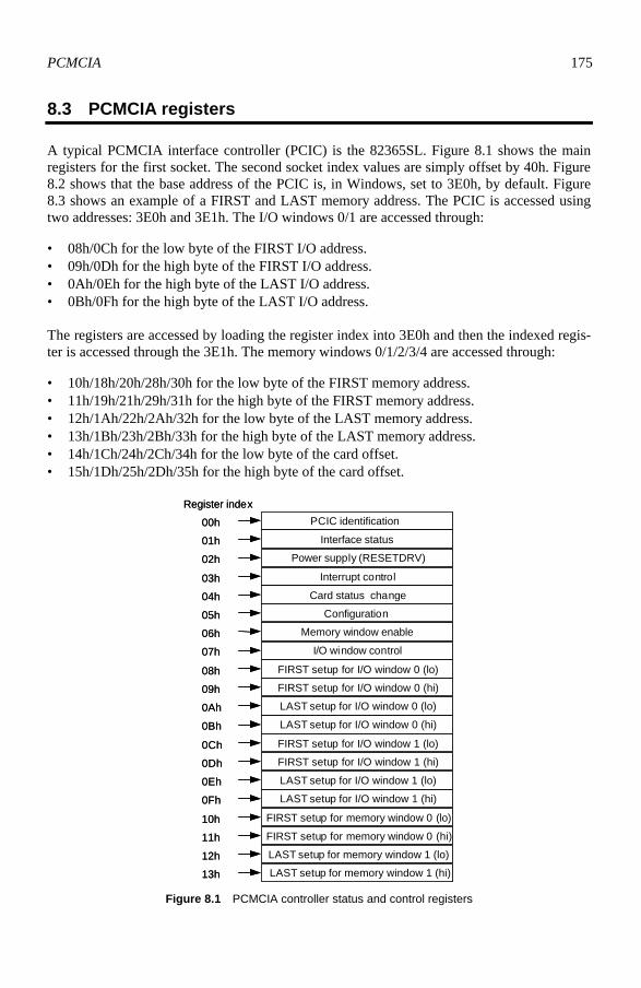
PCMCIA 175
8.3 PCMCIA registers
A typical PCMCIA interface controller (PCIC) is the 82365SL. Figure 8.1 shows the main registers for the first socket. The second socket index values are simply offset by 40h. Figure 8.2 shows that the base address of the PCIC is, in Windows, set to 3E0h, by default. Figure 8.3 shows an example of a FIRST and LAST memory address. The PCIC is accessed using two addresses: 3E0h and 3E1h. The I/O windows 0/1 are accessed through:
• 08h/0Ch for the low byte of the FIRST I/O address. • 09h/0Dh for the high byte of the FIRST I/O address. • 0Ah/0Eh for the high byte of the LAST I/O address. • 0Bh/0Fh for the high byte of the LAST I/O address. The registers are accessed by loading the register index into 3E0h and then the indexed regis-ter is accessed through the 3E1h. The memory windows 0/1/2/3/4 are accessed through:
• 10h/18h/20h/28h/30h for the low byte of the FIRST memory address. • 11h/19h/21h/29h/31h for the high byte of the FIRST memory address. • 12h/1Ah/22h/2Ah/32h for the low byte of the LAST memory address. • 13h/1Bh/23h/2Bh/33h for the high byte of the LAST memory address. • 14h/1Ch/24h/2Ch/34h for the low byte of the card offset. • 15h/1Dh/25h/2Dh/35h for the high byte of the card offset.
PCIC identification
Interface status
Power supply (RESETDRV)
Interrupt control
Card status change
Configuration
Memory window enable
I/O window control
FIRST setup for I/O window 0 (lo)
00h
01h
02h
03h
04h
05h
06h
07h
08h
09h
0Ah
0Bh
0Ch
FIRST setup for I/O window 0 (hi)
LAST setup for I/O window 0 (lo)
LAST setup for I/O window 0 (hi)
FIRST setup for I/O window 1 (lo)
FIRST setup for I/O window 1 (hi)
LAST setup for I/O window 1 (lo)
LAST setup for I/O window 1 (hi)
0Dh
0Eh
0Fh
10h FIRST setup for memory window 0 (lo)
FIRST setup for memory window 0 (hi)
LAST setup for memory window 1 (lo)
LAST setup for memory window 1 (hi)
11h
12h
13h
Register index
Figure 8.1 PCMCIA controller status and control registers

176 Computer busses
For example, to load a value of 22h into the Card status change register, the following would be used: _outp(0x3E0,5h); /* point to Card status change register */ _outp(0x3E1,22h); /* load 22h into Card status change register */
Figure 8.2 Start and end of shared memory
Figure 8.3 Base address of the PCIC

PCMCIA 177
8.3.1 Window enable register
The window enable register has a register index of 06h (and 46h for the second socket). The definition of the register is
Bit 7 IOW1 I/O window 1 enable (1)/ disable (0). Bit 6 IOW0 I/O window 0 enable (1)/ disable (0). Bit 5 DEC If active (1) MEMCS16 generated from A23–A12, else from A23–A17. Bit 4 MW4 Memory window 4 enable (1)/ disable (0). Bit 3 MW3 Memory window 3 enable (1)/ disable (0). Bit 2 MW2 Memory window 2 enable (1)/ disable (0). Bit 1 MW1 Memory window 1 enable (1)/ disable (0). Bit 0 MW0 Memory window 0 enable (1)/ disable (0).
8.3.2 FIRST set up for memory window
The FIRST window memory address is made up of a low byte and a high byte. The format of the high-byte register is
Bit 7 DS Data bus size: 16-bit (1)/ 8-bit (0). Bit 6 0WS Zero wait states: no wait states (1)/ additional wait states (0). Bit 5 SCR1 Scratch bit (not used). Bit 4 SCR0 Scratch bit (not used). Bit 3–0 Window start address A23–A20.
The format of the low-byte register is
Bit 7–0 A19–A12. Window start address A19–A12.
8.3.3 LAST set up for memory window
The LAST window memory address is made up of a low byte and a high byte. The format of the high-byte register is
Bit 7, 6 WS1, WS0 Wait state. Bit 5, 4 Reserved. Bit 3–0 A23–A20 Window start address A23–A20.
The format of the low-byte register is
Bit 7–0 Window start address A19–A12.
8.3.4 Card offset set up for memory window
The card offset memory address is made up of a low byte and a high byte. The format of the high-byte register is
Bit 7 WP Write protection: protected (1)/ unprotected (0). Bit 6 REG REGISTER SELECT enabled. If set to a 1 then access to attribute
memory, else common memory. Bit 5–0 Window start address A25–A20.

178 Computer busses
The format of the low-byte register is
Bit 7–0 Window start address A19–A12
8.3.5 FIRST set up for I/O window
The FIRST window I/O address is made up of a low byte and a high byte. The format of the high-byte register is
Bit 7–0 A15–A8 The format of the low-byte register is
Bit 7–0 A7–A8
8.3.6 LAST setup for I/O window
The LAST window I/O address is made up of a low byte and a high byte. The format of the high-byte register is
Bit 7–0 A15–A8. The format of the low-byte register is
Bit 7–0 A7–A8
8.3.7 Control register for I/O address window
The control register for the I/O address window is made up from a single byte. Its format is
Bit 7, 3 WS1, WS0 Wait states for window 1 and 0. Bit 6, 2 0WS1, 0WS0 Zero wait states for window 1 and 0. Bit 5, 1 CS1, CS0 IOIS16 source. Select IOIS16 from PC (1) or select data size from DS1 and DS0 (0). Bit 4, 0 DS1, DS0. Data size: 16-bit (1)/ 8-bit (0).
8.3.8 Examples
A typical application of the PCMCIA socket is to use it for a modem. This is an example of a program to set up a modem on the COM2 port. For this purpose, the socket must be set up to map into the I/O registers from 02F8h to 02FFh. The following code will achieve this: /* load 02f8 into FIRST and 02FFh into LAST registers */ _outp(0x3E0,08h); /* point to FIRST low byte */ _outp(0x3E1,f8h); /* load f8h into FIRST low byte */ _outp(0x3E0,09h); /* point to FIRST high byte */ _outp(0x3E1,02h); /* load 02h into FIRST high byte */ _outp(0x3E0,0Ah); /* point to LAST low byte */ _outp(0x3E1,ffh); /* load ffh into LAST low byte */ _outp(0x3E0,0Bh); /* point to LAST high byte */ _outp(0x3E1,02h); /* load 02h into LAST high byte */ /*setup control register: no wait states, 8-bit data access */

PCMCIA 179
_outp(0x3E0,07h); /* point to I/O Control register */ _outp(0x3E1,00h); /* load 00h into register */ /* enable window 0 */ _outp(0x3E0,06h); /* point to memory enable window */ _outp(0x3E1,04h); /* load 0100 0000b to enable I/O window 0 */
8.4 Exercises
8.4.1 How many data bits does the PCMCIA bus have: (a) 8 (b) 16 (c) 24 (d) 32 8.4.2 How are devices typically added to the system: (a) They are mapped into the I/O memory address (b) They directly into the physical address of the system (c) They use polled interrupts (d) They interface to a main controller 8.4.3 What is the base address of the registers that are used to program the PCMCIA
device: (a) 1E0h (b) 2E0h (c) 3E0h (d) 4E0h 8.4.4 Prove that the maximum address memory with PCMCIA is 64 MB. 8.4.5 Explain how I/O registers are used to program the PCMCIA device. 8.4.6 Show the lines of C code that would be required to mount a primary serial port
(3F8h–3FFh) and an ECP printer port (378h–37Ah). 8.4.7 Show the lines of C code that would be required to mount a primary (1F0h–1F7h)
and a secondary hard disk (170h–177h). 8.4.8 How would the programming for extra memory differ from an isolated I/O device.
8.5 Notes from the author
PCMCIA devices – To save paper, I’ve got seven lines to tell you about them. Well, in sum-mary, they’re really good, but tend to be relatively expensive. Their principle use is to add a network adapter or a modem to a notebook computer. They are typically not used to add to the memory of the notebook or to increase its hard disk space (an internal upgrade is much better for these). Personally, I find them a little too thin, and I do not believe they can get all the required electronics into them (but I remember when simple logic ICs, like AND and OR gates, were as big as your thumb and they could heat it if you required).

USB and Firewire
9.1 Introduction
The PC is now evolving into a powerful system through: • Microprocessor developments. • Improved graphics systems, such as AGP. • The PCI bus architecture, especially the PCI bridge. • Improved plug-and-play technology and automated set-up. The USB port aids in its ease
of connection. USB (Universal Serial Bus) allows for the connection of medium bandwidth peripherals such as keyboards, mice, tablets, modems, telephones, CD-ROM drives, printers and other low to moderate speed external peripherals in a tiered-star topology. Its basic specification is: • Isochronous (‘continuous’) transfers which supports audio and video. With isochronous
data transfers, devices transmit and receive data in a guaranteed and predictable fash-ion. USB also supports non-isochronous devices (the highest priority), and both isochronous and non-isochronous can exist at the same time.
• Standardised industry-wide plug-and-play specification, cables and connections. • Multiple-tiered hubs with almost unlimited expansion (with up to 127 physical de-
vices), and concurrent operations. • 12 Mbps transfer rate and different packet sizes. It supports many device bandwidth
requirements from a few kbps to 12 Mbps. • Wide range of device data rates by accommodating packet buffer size and latencies. • A hot-plug capability which allows peripherals to be connected without powering down
the computer. Dynamically attachable and reconfigurable peripherals. • Enhanced power management with system hibernation and sleep modes. • Self-identifying peripherals, automatic mapping of function to driver and configuration. • Support for compound devices which have multiple functions. • Flow control for buffer handling built into protocol. • Error handling/fault recovery mechanism. • Support for identification of faulty devices. • Simple protocol to implement and integrate.
9
182 Computer busses
USB is a balanced bus architecture which hides the complexity of the operation from the devices connected to the bus. The USB host controller controls system bandwidth. Each de-vice is assigned a default address when the USB device is first powered or reset. Hubs and functions are assigned a unique device address by USB software. Typical examples of USB connected devices are: • Digital speakers/ microphones. • Joysticks. • Scanners/ modems/ printers/ monitors. • Game controllers/ graphics tablets. • Video conferencing cameras. • Musical interfaces, such as MIDI.
9.2 USB
9.2.1 Physical USB connection
USB uses a four-wire cable to connect to devices. One pair of the twisted-pair lines gives the differential data lines (D+ and D–), while the other two gives a 5 V and a GND supply rail, as given in Table 9.1. Data transfer rate is up to 12 Mbps, with a 1.5 Mbps subchannel for low-data-rate devices (such as a mouse). A single unit can connect directly to the PC, but a hub is required when more than one device is connected. Each peripheral can extend up to 5 m from each hub con-nection, with a maximum of 127 different devices to a single PC.
Table 9.1 USB connections
Pin Name Description 1 VCC +5 VDC 2 D– Data– 3 D+ Data+ 4 GND Ground
9.2.2 Bus protocol
Each bus transaction involves the transmission of up to three packets. These are • Token packet transmission – on a scheduled basis, the host controller sends a USB
packet which describes the type and direction of a transaction, the USB device address and endpoint number. The addressed USB device selects itself by decoding the appropri-ate address fields.
• Data packet transmission – the source of the transaction then sends a data packet, or in-dicates it has no data to transfer.
• Handshake packet transmission – destination device responds with a handshake packet to indicate whether the transfer was successful.

USB and firewire 183
USB supports two types of transfers: stream and message. A stream has no defined structure, whereas a message does. At start-up one message pipe, Control Pipe 0, always exists as it provides access to the device’s configuration, status and control information. The USB protocol supports hardware or software error handling. In hardware error han-dling the host controller retries three times before informing the client software of the error. Each packet includes a CRC field which detects all single and double bit errors, as well as many multibit errors. Typically error conditions are short term. A major advantage of USB is the hot attachment and detachment of devices. USB does this by sensing when a device is attached or detached. When this happens, the host system is no-tified, and system software interrogates the device. It then determines its capabilities, and automatically configures the device. All the required drivers are then loaded and applications can immediately make use of the connected device.
9.2.3 Data transfers types
USB optimizes large data transfers and real-time data transfers. When a pipe is established for an endpoint, most of the pipe’s transfer characteristics are determined and remain fixed for the lifetime of the pipe. Transfer characteristics that can be modified are described for each transfer type. USB defines four transfer types: • Control transfers – bursty, non-periodic, host software initiated request/response com-
munication typically used for command/status operations. • Isochronous transfers – periodic, continuous communication between host and device
typically used for time relevant information. This transfer type also preserves the con-cept of time encapsulated in the data. This does not imply, however, that the delivery needs of such data are always time critical.
• Interrupt transfers – small data, non-periodic, low frequency, bounded latency, device initiated communication typically used to notify the host of device service needs.
• Bulk transfers – non-periodic, large bursty communication typically used for data that can use any available bandwidth and also is delayed until bandwidth is available.
9.2.4 USB implementation
There are two main ways to implement USB. These are:
• OHCI (open host controller interface). This method defines the register level inter-face that enables the USB controller to communicate with the host computer and the op-erating system. OHCI is an industry-standard hardware interface for operating systems, device drivers, and the basic input output system (BIOS) to manage the USB. It opti-mises performance of the USB bus while minimising central processing unit (CPU) overhead to control the USB. Its main features are:
• Scatter/gather bus master hardware support reduces CPU overhead to handle multiple data transfers across the USB.
• Efficient isochronous data transfers allow for high USB bandwidth without slowing down the host CPU.
• Assurance of full compatibility with all USB devices.

184 Computer busses
• UHCI (universal host controller interface). This method defines how the USB control-ler talks to the host computer and its operating system. It is optimised to minimise host computer design complexity and uses the host CPU to control the USB bus. Its main fea-tures are:
• Simple design reduces the transistor count required to implement the USB inter-face on the host computer, thus reducing system cost.
• Assurance of full compatibility with all USB devices. The PCI bridge device (PIIX3/PIIX4) contains a USB host controller (HC) with a root hub with two USB ports. This allows two USB peripheral devices to directly communicate with the PCI bridge without an external hub. When more than two USB devices require to be con-nected then an external hub can be added. The USB’s PCI configuration registers are located in the PCI configuration space. The host controller uses the UHCI standard and thus uses UHCI standard software driv-ers. It basically consists of two parts:
• Host controller driver (HCD). This is the software that manages the host controller operation and is responsible for scheduling the traffic on USB by posting and maintain-ing transactions in system memory. It interprets requests from the USBD and builds frame list, transfer descriptor, queue head, and data buffer data structures for the host controller. These data structures are built in system memory and contain all necessary information to provide end-to-end communication between client software in the host and devices on the USB. The host controller moves data between system memory and devices on the USB by processing these data structures and generating the transaction on USB. The host controller executes the schedule lists generated by HCD and reports the status of transactions on the USB to HCD. Command execution includes generating serial bus token and data packets based on the command and initiating transmission on USB. For commands that require the Host Controller to receive data from the USB de-vice, the host controller receives the data and then transfers it to the system memory pointed to by the command. The UHCI’s HCD provides sufficient commands and data to keep ahead of the host controller execution and analyses the results as the commands are completed.
• Host controller (HC). The host controller interfaces to the USB system software in the host via the HCD.
Attachment of USB devices
All USB devices attach to the USB via a port on specialised USB devices known as hubs. Hubs indicate the attachment or removal of a USB device in its per port status. The host que-ries the hub to determine the reason for the notification. The hub responds by identifying the port used to attach the USB device. The host enables the port and addresses the USB device with a control pipe using the USB Default Address. All USB devices are addressed using the USB Default Address when initially connected or after they have been reset. The host deter-mines if the newly attached USB device is a hub or a function and assigns a unique USB address to the USB device. The host establishes a control pipe for the USB device using the assigned USB address and endpoint number zero. If the attached USB device is a hub and USB devices are attached to its ports, then the above procedure is followed for each of the

USB and firewire 185
attached USB devices. If the attached USB device is a function, then attachment notifications will be dispatched by USB software to interested host software.
Removal of USB devices
When a USB device has been removed from one of its ports, the hub automatically disables the port and provides an indication of device removal to the host. Then the host removes knowledge of the USB device. If the removed USB device is a hub, the removal process must be performed for all of the USB devices that were previously attached to the hub. If the removed USB device is a function, removal notifications are sent to interested host software.
USB host: hardware and software
The USB host interacts with USB devices through the host controller. The host is responsible for the following: • Detecting the attachment and removal of USB devices • Managing control flow between the host and USB devices • Managing data flow between the host and USB devices • Collecting status and activity statistics • Providing a limited amount of power to attached USB devices USB system software on the host manages interactions between USB devices and host-based device software. There are five areas of interactions between USB system software and de-vice software, they are: • Device enumeration and configuration. • Isochronous data transfers. • Asynchronous data transfers. • Power management. • Device and bus management information. Whenever possible, USB software uses existing host system interfaces to manage the above interactions. For example, if a host system uses Advanced Power Management (APM) for power management, USB system software connects to the APM message broadcast facility to intercept suspend and resume notifications.
9.2.5 USB host controller registers
VID (vendor identification register)
Address offset 00–01h Default value 8086h Attribute Read only
The VID register contains the vendor identification number. This register, along with the device identification register, uniquely identifies any PCI device. Writes to this register have no effect. Bit description 15:0 vendor identification number. This is a 16-bit value assigned to Intel.

186 Computer busses
DID (device identification register)
Address offset 02–03h Default value 7112h Attribute Read only
The DID register contains the device identification number. This register, along with the VID register, defines the USB host controller.
9.3 Firewire
The main competitor to USB is the Firewire standard (IEEE 1394-1995) which is a high-speed serial bus for desktop peripheral devices, typically for video transfers. It supports rates of approximately 100, 200 and 400 Mbps, known as S100, S200 and S400 respectively. Future standards promise higher data rates, and ultimately it is envisaged that rates of 3.2Gbps will be achieved when optical fibre is introduced into the system. It is generally more expensive than USB to implement for both the host computer and peripherals. Its main features are: • 100/200/400 Mbps transfer rate. • Point-to-point interconnect with a tree topology; 1000 buses with 64 nodes gives 64 000
nodes. • Automatic configuration and hot plugging. • Isochronous data transfer, where a fixed bandwidth is dedicated to a particular periph-
eral. • Maximum cable length of 4.5m. Firewire also complements USB in that it supports high-speed peripherals, whereas USB supports low-to-medium speed peripherals. It is an attractive alternative to technologies such as SCSI and it may provide a universal connection to replace many of the older connectors normally found at the back of a standard PC. This should subsequently reduce the costs of production of computer interfaces and peripheral connectors, as well as simplifying the re-quirements placed on users when setting up their devices. This is made possible by the fol-lowing features of the IEEE-1394 bus: • Hot pluggable – devices can be added or removed while the bus is still active. • Easy to use – there are no terminators, device addressing or elaborate configuration of-
ten associated with technologies like SCSI. • Flexible topology – devices can be connected together in many configurations, thus the
user need not consider logical locations on the network. • Fast – suitable for high bandwidth applications. • Rate mixing – a single cable medium can carry a mix of different speed capabilities at
the same time • Inexpensive – targeted at consumer devices.

USB and firewire 187
9.3.1 Topology
There are two bus categories: • Cable. This is a bus which connects external devices via a cable, The cable environment
is a non-cyclic network with finite branches consisting of bus bridges and nodes (cable devices). Non-cyclic networks contain no loops and results in a tree topology, with de-vices daisy-chained and branched (where more than one device branch is connected to a device). Figure 9.1 shows an example of an IEEE-1394 Splitter which has three branches and the telephone is daisy-chained from the digital camera. The finite branches restriction imposes a limit of 16 cable hops between nodes. There-fore branching should be used to take advantage of the maximum number of nodes on a bus. 6-bit node addressing allows up to 63 nodes on each bus, while 10-bit bus address-ing allows up to 1023 buses, interconnected using IEEE-1394 bridges. Devices on the bus are identified by node IDs. Configuration of the node IDs is performed by the self ID and tree ID processes after every bus reset. This happens every time a device is added to or removed from the bus, and is invisible to the user. A final restriction is that, using standard cables, the length between nodes is limited to 4.5m. This can be increased by adding repeaters between nodes, but lengths are expected to improve as work on the standard ensues. Although a PC is shown in Figure 9.1, a principal advantage of IEEE-1394 is that, unlike USB, no PC is actually required to form a bus, and devices can talk to each other without intervention from a computer.
• Backplane. This type is an internal bus. An internal IEEE-1394 device can be used alone, or incorporated into another backplane bus. For example, two pins are reserved for a serial bus by various ANSI and IEEE bus standards. Implementation of the back-plane specification lags the development of the cable environment, but one could image internal IEEE-1394 hard disks in one computer being directly accessed by another IEEE-1394 connected computer.
PC PC
DVD DVD
IEEE-1394 Splitter
IEEE-1394 splitter
Digital Camera Digital
Camera
Printer Printer
TV/Stereo TV/Stereo
Telephone Telephone
Figure 9.1 IEEE-1394 topology example

188 Computer busses
9.3.2 Asynchronous and isochronous transfer
One of the key capabilities of IEEE-1394 is isochronous data transfer. Both asynchronous and isochronous are supported, and are useful for different applications. Isochronous trans-mission transmits data like real-time speech and video, both of which must be delivered uninterrupted, and at the rate expected, whereas asynchronous transmission is used to transfer data that is not tied to a specific transfer time. With IEEE-1394, asynchronous is the conventional transfer method of sending data to an explicit address, and receiving confirmation when it is received. Isochronous, however, is an unacknowledged guaranteed-bandwidth transmission method, useful for just-in-time delivery of multimedia-type data. An isochronous ‘talker’, requests an amount of bandwidth and a channel number. Once the bandwidth has been allocated, it can transmit data preceded by a channel ID. The isochronous listeners can then listen for the specified channel ID and accept the data follow-ing. If the data is not intended for a node, it will not be set to listen on the specific channel ID. Up to 64 isochronous channels are available, and these must be allocated, along with their respective bandwidths, by an isochronous resource manager on the bus. Figure 9.2 shows an example situation where two isochronous channels are allocated. These have a guaranteed bandwidth, and any remaining bandwidth is used by pending asyn-chronous transfers. Thus isochronous traffic takes some priority over asynchronous traffic. By comparison, asynchronous transfers are sent to explicit addresses on the 1394 bus (Figure 9.3). When data is to be sent, it is preceded by a destination address, which each node checks to identify packets for itself. If a node finds a packet addressed to itself, it copies it into its receive buffer. Each node is identified by a 16-bit ID, containing the 10-bit bus ID and 6-bit node or physical ID. The actual packet addressing, however, is 64 bits wide, pro-viding a further 48 bits for addressing a specific offset within a node’s memory. This ad-dressing conforms to the control and status register (CSR) bus architecture standard. The ISO/IEC 13213:1994 minimises the amount of circuitry required by 1394 ICs to interconnect with standard parallel buses. The 48-bit offset allows for the addressing of 256 terabytes of memory and registers on each node.
Isochronous channel #1 time slot
Isochronous channel #2 time slot
Time slot available for asynchronous transport
Packet frame = 125 µs
Timing indicator
Isochronous channel #1 time slot
Isochronous channel #2 time slot
Time slot available for asynchronous transport
Packet frame = 125 µs
Timing indicator
Figure 9.2 Bandwidth allocation on the IEEE-1394 bus

USB and firewire 189
Destination ID (16 bits)
Data length (16 bits) Extended tcode (16 bits)
Header CRC (32 bits)
Zero padded bytes (8n bits)
Data CRC (32 bits)
Data field
tl (6 bits)
rtl (2 bits)
tcode (4 bits)
prl (4 bits)
Destination offset (48 bits)
Source ID (16 bits)
Figure 9.3 Asynchronous write data block payload
9.3.3 IEEE-1394 packet formats There are a number of different packet formats specified in 1394-1995, however only the asynchronous block write will be presented here, as it is the main transaction type used within this project. The asynchronous block write is described in the 1394-1995 specification as a packet type that requests a data block be written to the specified destination address. It is the packet type used on asynchronous transmits, for a variable length of data. The destination_ID field should contain the 16-bit destination node ID, while the destina-tion_offset field contains the remaining 48 bits required for CSR addressing. The data is sent in the data field, which can be any quadlet-aligned length up to a maximum given by the transmission speed. At 200 Mbps, for example, the data field may hold anything from 0 to 1024 bytes, in stages of four bytes. The header information is followed by a CRC (cyclic redundancy check) for error checking, as is the block of data.
9.3.4 Bus management Two bus management entities are available in the cable environment: the isochronous re-source manager and the bus manager. They provide services such as maintaining topology maps, or acting as a central resource from which bandwidth and channel allocations can be made. Further information on bus management can be found in the 1394-1995 specification.
9.3.5 Cable Figure 9.4 shows that the 1394 cable consists of three individually shielded cable pairs. There are two power lines and two (screened) twisted pairs for data and strobe transmission.
9.3.6 Transmission rates As already discussed, the cable rate definitions for 1394-1995 are termed S100, S200 and S400, give actually data rates of 98.304Mbps, 196.608Mbps and 393.216Mbps, respec-tively. The high data rates are achieved by using differential non-return to zero (nrz), signal-ling on each shielded twisted pair.

190 Computer busses
Figure 9.4 IEEE-1394 cable and connectors
9.4 Exercises
9.4.1 How many USB ports are available from the host controller on a PC (PIIX3/4): (a) 1 (b) 2 (c) 4 (d) 8 9.4.2 Discuss the advantages of USB connected devices over: (i) ISA devices (ii) PCI devices (iii) Serial/parallel port connected devices 9.4.3 Outline the main difference between isochronous and asynchronous data traffic. In
which applications is it isochronous. 9.4.4 Outline the main types of data transfer on the USB port. 9.4.5 By searching the Internet or a computer catalogue, locate some USB connected
devices.
9.5 Notes from the author
Congratulations go to the USB port. It was the first truly generic, easy-to-use, connection bus for the PC that has mechanisms for non-real-time (such as printer data) and real-time data (such as video, audio and speech). It allows for the easy addition and removal of de-vices from the system, and it also supports hot plugging (adding or removing a device while the computer is on). Microsoft first supported USB in Windows 95 OSR2, and it has since become one of the most used ports, for devices such as video cameras, CD-ROM drives, printers, digital speakers, monitors, and so on. The only problem with USB is that it only gives a data throughput of 12 Mbps, and thus cannot be used for high-speed devices. Possi-bly, over time, this rate may be increased, or other faster busses, such as Firewire could be used for high-speed applications, such as Fast Ethernet, multimedia communications, hard disk interfaces, and so on. The IEEE-1394 specification (or i.LINK) is now being used on some systems (especially in notebooks). Its adoption as a standard interface device will depend on whether new stan-dard for the USB specification increase the transfer bit rate to support, at least, 100Mbps. When the USB port can do this, there will be a lesser need for IEEE-1394.

Games Port, Keyboard and Mouse
10.1 Introduction
PCs have traditionally been difficult to connect to and set up, for reasons such as:
• Different connectors – there are so many different types of connectors for many different types of devices that connect to the PC. For example, the keyboard uses a 5-pin DIN plug, the parallel port uses a 25-pin D-type connector, the primary serial port uses a 9-pin D-type connector, the video adaptor uses a 15-pin D-type connector, and so on. The future is likely to bring a standardisation of these connectors, possibly with the USB port.
• Different configurations – typically different peripherals required assigned interrupts and I/O addresses. For example, the keyboard uses IRQ1 and I/O ports at 60h and 64h. This is now being overcome by busses such as SCSI and USB, which only require a sin-gle interrupt and a limited range of addresses. They also cope better with hot plug-and-play devices and operating system configurable devices.
• Different data traffic rates – relatively low speed interfaces, such as the ISA bus, have often reduced the rate of other faster busses, such as the PCI bus. This is now being overcome by the use of bridges and the USB bus.
The games port, the keyboard and the mouse are also relatively slow devices which, in their standard form, all have different connectors. In the future PCs may standardise these low- and medium-speed devices on the USB port. The keyboard port and mouse port are now standard items on a PC, and most PCs now have a games port, which supports up to two joy-sticks. Most PCs support either a PS/2-style mouse or one connected to the serial port (COM1: or COM2:). The operating system automatically scans all the mouse and keyboard ports to determine where the mouse is connected to, and whether there is a keyboard connected. Typically, these days, a mouse connects to the PS/2 port, which is basically an extension of the keyboard port. The keyboard connects to either a 5-pin DIN plug, or more typically on modern PCs to a smaller 5-pin plug. With the smaller connector, the PS/2 mouse and the keyboard can share the same port (this is typical in new PCs and also for notebooks).
10.2 Games port
The PC was never really designed to provide extensive games support, but as it is so general purpose, it is now used to run arcade style games. A mouse is well designed for precise
10

192 Computer busses
movements and to select objects, but is not a good device to play games with; thus, a joystick is typically used. The games port adapter supports up to two joysticks connected to the same port. It has 15 pins, which are outlined in Table 10.1 and connects to the system via:
• Lower eight bits of the data bus.
• Lower 10 bits of the address bus.
• IOR and IOW .
Table 10.1 Game adapter connections
Pin Description Pin Description 1 +5V 9 +5V 2 1st button for joystick A (BA1) 10 1st button for joystick B (BB1) 3 X-potentiometer of joystick A (AX) 11 X-potentiometer of joystick B (BX) 4 GND 12 GND 5 GND 13 Y-potentiometer of joystick B (BY) 6 Y-potentiometer of joystick A (AY) 14 2nd button for joystick B (BB1) 7 2nd button for joystick A (BA1) 15 +5V 8 +5V Each joystick has two buttons, which are normally open circuit, and two potentiometers which give a variable resistance from 0 Ω to 100 kΩ, to indicate the x- and y-position of the joystick handle. Figure 10.1 shows its connections. An unpressed button corresponds to a high level and a button press to a low level.
GND
GND
GND
GND
1
9
2
10
3
11
4
12
5
13
6
14
7
15
8
Joystick A Joystick B
BA1
BA2
AX
AY
BB1
BB2 BY
BX
Figure 10.1 Joystick interface

Games port, keyboard and mouse 193
Figure 10.2 Memory map showing Gameport I/O address
The status of the button can be determined by reading the 201h address (see Figure 10.2), its format is given in Figure 10.3. Thus to test for a button press the upper four bits of the regis-ter are tested to determine if they are a zero. Figure 10.4 shows a simple C program to test the status of the buttons.
BB2 BB1 BA2 BA1 BY BX AY AX
Joys
tick
B:
Bu
tto
n 2
Joys
tick
B:
Bu
tto
n 1
Joys
tick
A:
Bu
tto
n 2
Joys
tick
B:
Bu
tto
n 1
Joys
tick
B:
Y-p
ote
ntio
me
ter
sta
tus
Joys
tick
B:
X-p
ote
ntio
me
ter
sta
tus
Joys
tick
A:
Y-p
ote
ntio
me
ter
sta
tus
Joys
tick
A:
X-p
ote
ntio
me
ter
sta
tus
Address: 201h
Figure 10.3 Joystick status register format
The reading of the position of the joystick is a little more difficult. For this an event is triggered by writing to the status register. This triggers a one-shot multivibrator, the status of which is given on the lower four bits of the status register, which change from a zero to a one when it has completed the single-shot. The resistance is given by
( )Ω
−=
011.0
2.24ìs interval TimeResistance

194 Computer busses
Figure 10.4 Simple C program to test joystick button status
Thus, the timing values will change from 24.2 µs (for 0 kΩ) to 1.124 ms (for 100 kΩ). A sim-ple program that determines the time it takes for AX to be set is given next:
2 Program 10.1 #include <stdio.h> #include <conio.h> int main(void) unsigned int inval, start1, start2, start, end1, end2, end; do _outp(0x43,0); /* Specify Counter 0 */ start1=_inp(0x40); /* get LSB of Counter 0 */ start2=_inp(0x40); /* get MSB of Counter 0 */ _outp(0x201,0); /* start one-shot */ do inval=_inp(0x201); /* read button status of joystick */ while ((inval & 1)==1); /* wait till set to a 0 */ _outp(0x43,0); /* Specify Counter 0 */ end1=_inp(0x40); /* get LSB of Counter 0 */ end2=_inp(0x40); /* get MSB of Counter 0 */

Games port, keyboard and mouse 195
start=(start1 &0xff)+((start2 &0xff)<<8); end=(end1 & 0xff)+((end2 & 0xff)<<8); if (start>end) printf("Value = %u\n",start-end); else /* roll-over has occurred */ printf("Value = %u\n",start+(0xffff-end)); while (!kbhit()) ; return(0); Program 10.1 uses Counter 0 which is loaded from address 40h. It has a 16-bit counter regis-ter and has a 1.2 MHz clock as its input. It thus rolls-over every 55 ms. In a sample test run of the above program the output value varied from 62 to 2740, with a static value of 1400. The joystick could be easily calibrated with these values, which are the extremes for either x or y. Note that AY is tested with: do inval=_inp(0x201); /* read button status of joystick */ while ((inval & 2)==1); /* wait till set to a 0 */
and BX is tested with: do inval=_inp(0x201); /* read button status of joystick */ while ((inval & 4)==1); /* wait till set to a 0 */
10.3 Keyboard
Figure 10.5 shows the main connections in the keyboard interface. It uses a 5-pin DIN socket for the connection. The data is sent from the keyboard to the PC in an 11-bit SDU (serial data unit) format over the KBD Data line. When a key has been pressed the IRQ1 interrupt line is activated. The keyboard interface IC scans the keys on the keyboard by activating the X-decoder lines and then sensing the Y-decoder lines to see if there has been a keypress. It then decodes this to sense if a key has changed its state. It then converts the keypress or release to a code which it sends to the keyboard controller on the PC. The format of the code is in the form of an RS-232 interface with eight data bits, one parity bit, one start bit and one stop bit. Unlike RS-232, it uses a synchronous transfer where the clock speed is defined by the KDB clock line. It is very unlikely that a programmer would ever need to interface directly with the key-board, as there are a whole host of standard functions that are well tested and interface well with the operating system. It is always advisable to use the standard input keyboard func-tions, over direct interfacing. Typically the operating system takes over control of all input key presses and sends these to the required process, thus it is not a good idea to interrupt the flow.

196 Computer busses
X-D
eco
de
r
Y-Decoder
Scan matrix
Keyboard
Interface IC (K
/B)
Keyboard
Controller IC
(PC
)
11-bitSDUcode
IRQ1
D0-D7
(1) KBD Clock
(4) GND
(2) KDB Data
(3) KBD Reset
(5) +5V
Figure 10.5 Keyboard interface
The keyboard uses two I/O addresses. These are shown in Figure 10.6, and are:
• Input/output buffer (address: 60h) – used to read the code from the keyboard.
• Control/status register (address: 64h) – used either to determine the status of the key-board (when a value is read from the register) or to set up the keyboard (when a value is written to the register). The commands used are listed in Table 10.2. On a read opera-tion, it acts as a status register. Figure 10.7 shows the bit definitions, these are:
Figure 10.6 Keyboard I/O addresses (60h and 64h)

Games port, keyboard and mouse 197
PARE Parity bit – 1 = last byte has a parity error, 0 = no error. TIM General time-out – 1 = error, 0 = no error. AUXB Output buffer for auxiliary device – 1 = holds data for auxiliary device,
0 = holds keyboard data. KEYL Keyboard lock status – 1 = keyboard unlocked, 0 = keyboard locked. C/D Command/data – 1 command byte written via port 64h, data byte writ-
ten via port 60h. SYSF. System flag – 1 = self-test successful, 0 = power-on reset. INPB. Input buffer status – 0 = Data in input buffer, 0 = no data. OUTB. Output buffer status – 0 = Controller data in output buffer, 0 = buffer
empty. The auxiliary device is typically a PS/2 style mouse. Program 10.2 shows an example pro-gram which reads from the keyboard buffer. It disables the IRQ1 interrupt. (Note that this may cause some systems to not respond to the keyboard if the program does not terminate properly.)
PARE TIM AUXB KEYL C/D SYSF INPB OUTB Address: 64hStatus register
Figure 10.7 Status register bits
Table 10.2 Control register commands
Code Command Return value (in output buffer)
a7h Disable auxiliary device a8h Enable auxiliary device a9h Check interface to auxiliary device 00h = no error, 01h = clock line low, 02h = clock
line high, 03h = data line low, 04h = data line high and ffh = no auxiliary device.
aah Self-test 55h, on success abh Check keyboard interface 00h = no error, 01h = clock line low, 02h = clock
line high, 03h = data line low, 04h = data line high and ffh = no auxiliary device
adh Disable keyboard aeh Enable keyboard c0h Read input port c1h Read input port (low) c2h Read input port (high) d0h Read output port d1h Write output port d2h Write keyboard output buffer d3h Write output buffer of auxiliary device d4h Write auxiliary device e0h Read test input port

198 Computer busses
2 Program 10.2 /* This program may not work in Windows 95/98/NT/2000 */ /* as it tries to take direct control of the keyboard */ #include <stdio.h> #include <conio.h> int main(void) unsigned int inval, hit=0; char ch; _outp(0x21,0x02); /* disable IRQ1 */ do do inval=_inp(0x64); /* read status register */ if ((inval & 0x01)==0x01) /* set for output buffer */ puts("Key pressed"); ch=_inp(0x60); /* read key from buffer */ printf("%c",ch); hit=1; while (hit==0); hit=0; if (ch==0x1) break; /* wait for ESC key */ while (1); _outp(0x21,0); /* enable IRQ1 */ return(0);
10.4 Mouse and keyboard interface
Modern PCs typically use the 8242 device to provide for a PS/2 mouse and keyboard func-tion, as illustrated in Figure 10.8. It can be seen that the two interrupts which are available are IRQ1 (the keyboard interrupt) and IRQ12 (PS/2 style mouse). If the mouse connects to the serial port then the IRQ12 line does not cause an interrupt. All clock frequencies are derived from the keyboard clock frequency (see Figure 10.8). Notice that the interface for the PS/2-style mouse is identical to the keyboard connection. They are interfaced through the same registers (60h and 64h).
8242PCPL
KBDCLK
MSCLK
KBDATA
KBDCLK
+5V
GND
MSDATA
MSCLK
+5V
GND
Mouseinterface
K/Binterface
IRQ1
IRQ12
MSDATA
KBDATA
KBCLK
DD[7:0]
IOR#
IOW#
KEYLOCK
Figure 10.8 Mouse and keyboard interface

Games port, keyboard and mouse 199
10.5 Mouse
Typically on modern PCs the PS/2-style mouse is preferred over serial port mice. PS/2-style mice free up the serial port for other uses, such as for data transfers, modem connections, and so on. Table 10.3 outlines the commands that can be used to program the mouse.
Table 10.3 Control register commands
Code Command Description e6h Reset scaling
e7h Set scaling
e8h Set resolution Sets the resolution: 00h = 1 count/mm, 01h = 2 counts/mm, 02h = 4 counts/mm and 03 = 8 counts/mm.
e9h Determine status 3 status bytes Byte 1: Bit 0: Right mouse button pressed (if 1). Bit 2: Left mouse button pressed (if 1). Bit 4: Scaling (0=1:1, 1=1:2). Bit 5: Mouse (0=enabled, 1=disabled). Bit 6: Mode (0=stream, 1=remote). Byte 2: Resolution. Byte 3: Sample rate.
eah Set stream mode
ebh Read data Reads an 8-byte data packet from the mouse.
ech Resets mouse to normal mode
eeh Sets mouse to wrap mode In wrap mode all the commands or data sent to the mouse.
f0h Set remote mode
f2h Identify unit 00h = mouse
f3h Set sampling rate Sampling rate is then set by the value put into output buffer: 0ah = 10 samples/s, 14h = 20 samples/s, 28h = 40 samples/s, 3c = 60 samples/s, 50h = 80 samples/s, 64h = 100 samples/s and c8h = 200 samples/s.
f4h Enable mouse
f5h Disable mouse
f6h Set standard mouse to stan-dard values
feh Resend
ffh Reset
The PS/2 mouse is programmed by:

200 Computer busses
• Sending the write auxiliary device (d4h) command to 64h (Control register).
• The next byte is a command code which is sent to port 60h, and then transferred to the mouse port (valid codes are given in Table 10.3). This command transfer only occurs for a single transfer.
The mouse can either be set into a stream mode or a remote mode, and writes movement data into the keyboard buffer. In stream mode, the mouse transmits movement data when it is moved by a given amount (set by the sample rate). In remote mode the mouse only transfers movement data when there is a specific read data command. When the read data command is sent, the 8-byte data packet is read from the addresses as specified in Table 10.4. An example of programming the mouse is given next: _outp(0x64,0xd4); /* Write aux. device */ do inval=_inp(0x64); while ((inval & 0x02)==0x02); /* wait until input buffer empty */ _outp(0x60,0xe7); /* set scaling */
Table 10.4 Control register commands
Offset Description 00h Bit 7: YOV (Y-data overflow), Bit 6: XOV (X-data overflow),
Bit 5: YNG (Y-value negative), Bit 4: XNG (X-value negative), Bit 1: RIG (right button pressed), Bit 0: LEF (left button pressed).
02h X-data movement since last access
04h Y-data movement since last access
10.6 Exercises
10.6.1 What is the base address of the joystick port: (a) 101h (b) 201h (c) 301h (d) 401h 10.6.2 Which I/O port addresses are used for the keyboard: (a) 60h, 64h (b) 160h, 164h (c) 260h, 264h (d) 360h, 364h 10.6.3 How is the x position and y position determined: (a) The time for a single-shot (b) A voltage level (c) An electrical current (d) A value in a register

Games port, keyboard and mouse 201
10.6.4 What interrupt does the keyboard use: (a) IRQ1 (b) IRQ3 (c) IRQ4 (d) IRQ12 10.6.5 What interrupt does the PS/2 style mouse use: (a) IRQ1 (b) IRQ3 (c) IRQ4 (d) IRQ12 10.6.6 Run the program in Figure 10.4 and show that the joystick buttons are working.
Modify the program so that it only displays a change of status in a button press (rather that scrolling down the screen). For example:
if ((inval & 0x80) == 1) && (button==0)) button=1; puts(“B:Button 2 Press”); if ((inval & 0x80) == 0) && (button==1)) button=0; puts(“B:Button 2 Reset”); 10.6.7 Run Program 10.1 and test the movement detection. Modify it so that it detects the
y movement. 10.6.8 Run Program 10.1 so that the user can calibrate the joystick. The user should be
asked to move the joystick to its maximum x directions, and also the maximum y directions. From this write a program which displays the joystick movement as a value from –1 to +1.
10.7 Notes from the author
Phew. I’m glad I got these three interfaces out of the way, in a single chapter. All three are based on a legacy type system. Over time, the USB port should replace each interface type, but as they work well at the present they may be around for a while longer. The method that the games port uses to determine position is rather cumbersome, where it uses a single-shot monostable timer to determine the x and y positions. An improved method is to pass the data using a serial interface, just as the mouse does. But, it’s a stan-dard, and that’s the most important thing. The keyboard and PS/2-style mouse connections have proved popular, as they are both now small 5-pin DIN-style connectors, and as the software automatically scans the port for devices, they can be plugged into either socket. This allows for an extra keyboard or a sec-ond mouse to be used with a notebook. As I’ve got a few extra lines at the end of this chapter, I would like to review the material that has been covered up to this point. The key to understanding internal busses is contained in the Motherboard chapter, where the processor interfaces with the TXC device, which di-rects any requests to the second-level cache, the DRAM memory or the PCI bus. The PCI bridge device is also important as it isolates the other busses, such as ISA/IDE, USB, se-rial/parallel port from the PCI bus, and thus the rest of the system. The keyboard, games port and mouse interfaces are accessed via the PCI bridge.
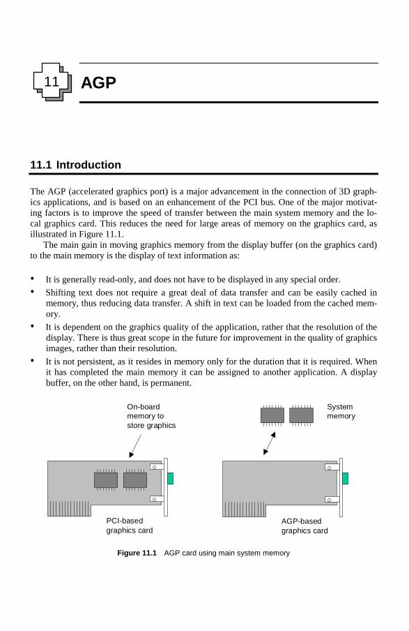
AGP
11.1 Introduction
The AGP (accelerated graphics port) is a major advancement in the connection of 3D graph-ics applications, and is based on an enhancement of the PCI bus. One of the major motivat-ing factors is to improve the speed of transfer between the main system memory and the lo-cal graphics card. This reduces the need for large areas of memory on the graphics card, as illustrated in Figure 11.1. The main gain in moving graphics memory from the display buffer (on the graphics card) to the main memory is the display of text information as: • It is generally read-only, and does not have to be displayed in any special order. • Shifting text does not require a great deal of data transfer and can be easily cached in
memory, thus reducing data transfer. A shift in text can be loaded from the cached mem-ory.
• It is dependent on the graphics quality of the application, rather that the resolution of the display. There is thus great scope in the future for improvement in the quality of graphics images, rather than their resolution.
• It is not persistent, as it resides in memory only for the duration that it is required. When it has completed the main memory it can be assigned to another application. A display buffer, on the other hand, is permanent.
PCI-basedgraphics card
AGP-basedgraphics card
Systemmemory
On-boardmemory tostore graphics
Figure 11.1 AGP card using main system memory
11
204 Computer busses
The 440LX is the first AGPset product designed to support the AGP interface. The HOST BRIDGE AGP implementation is compatible with the accelerated graphics port Specification 1.0. HOST BRIDGE supports only a synchronous AGP interface, coupling to the host bus frequency. The AGP interface can reach a theoretical ~532 Mbytes/sec transfer rate. The actual bandwidth will be limited by the capability of the HOST BRIDGE memory subsys-tem.
11.1.1 PCI interface
The HOST BRIDGE PCI interface is 33-MHz Revision 2.1 compliant and supports up to five external PCI bus masters in addition to the I/O bridge (PIIX4). HOST BRIDGE supports only synchronous PCI coupling to the host bus frequency. HOST BRIDGE defines a sophisticated data buffering scheme to support the required level of concurrent operations and provide adequate sustained bandwidth between the DRAM subsystem and all other system interfaces (CPU, AGP and PCI).
11.2 PCI and AGP
AGP defines the master as the graphics controller and the corelogic as the graphics card. The AGP interface is based on the 66 MHz PCI standard, but has four additional exten-sions/enhancements. These extensions are: • Deeply pipelined memory read and write operations, which fully hide memory access
latency. • Address bus and data bus demultiplexing, allowing for nearly 100% bus efficiency. • Extension to the PCI timing cycle which allows for one or two data transfers per 66 MHz
clock cycle. This provides a maximum data rate of 500 MB/s. • Extension to the PCI timing cycle which allows for four data transfers per 66 MHz clock
cycle. This provides for a maximum data rate of 1GB/s. All these enhancements are implemented using extra signal lines (sideband signals), and it is not intended as a replacement to the PCI bus. The AGP is physically, logically and electri-cally independent of the PCI bus, and has its own connector which is reserved solely for graphics devices (and is not interchangeable with the AGP connector). Figure 11.2 shows the main AGP signal lines. AGP uses deep pipelining which allows the total memory READ throughput equal to that which is possible for memory WRITE (in PCI the memory read throughput is about half of memory write throughput, as memory read access time is visible as wait states on this un-pipelined bus). This and optional higher transfer rates and address demultiplexing, allows for a large increase in memory read throughput over standard PCI implementations.

AGP 205
.
SBA[7:0]
AGP AGP
connectorAGP
connector
PIPE
RBF
WBF
ST[2:0]
/AD_STB0AD_STB0
/AD_STB1AD_STB1
/SB_STB1SB_STB1
CLK
GFRAME
GIRDYGTRDYGSTOP
GDEVSELGPERR
GSERRGREQ
GGNT0]:GAD[15
0]:GC/BE[3
GPAR
AGPaddressing
AGPflowcontrol
AGPstatus
AGPclocks/strobe
PCIsignals
SBA[7:0]
AGP AGP
connectorAGP
connector
PIPEPIPE
RBFRBF
WBFWBF
ST[2:0]
/AD_STB0AD_STB0 /AD_STB0AD_STB0
/AD_STB1AD_STB1/AD_STB1AD_STB1
/SB_STB1SB_STB1 /SB_STB1SB_STB1
CLK
GFRAMEGFRAME
GIRDYGIRDYGTRDYGTRDYGSTOPGSTOP
GDEVSELGDEVSELGPERRGPERR
GSERRGSERRGREQGREQ
GGNTGGNT0]:GAD[15 0]:GAD[15
0]:GC/BE[3 0]:GC/BE[3
GPARGPAR
AGPaddressing
AGPflowcontrol
AGPstatus
AGPclocks/strobe
PCIsignals
Figure 11.2 The main AGP signal lines
11.3 Bus transactions
AGP uses two types of bus operation. These are: • Queuing requests. This can be done over the SBA port, or the AD bus, and is set up
using Bit 9 for the status register (only one type at a time can be used). With the SBA port, the AD bus cannot be used, and vice versa. The sideband signals (SBA[7:0]) are used exclusively to transmit AGP access requests (all PCI transactions use the AD pins for both data and address), and are sent from the master to the core logic (the AGP re-quests are the same when sent over the AD bus or the SBA bus). A master that uses the SBA port does not require the PIPE signal which is used only to frame requests on the AD pins.
• Address demultiplexing option. This allows the complete AGP access request to be transmitted over the 8-bit SBA port. For this the request is broken into three parts: low- order address bits and length (type 1), mid-order address bits and command (type 2), and high-order address bits (type 3).
11.4 Pin description
AGP adds an extra 21 signal lines to the PCI specification. The basic implementation of AGP should support ×1 and ×2 transfer rates, and may optionally support ×4 data transfer rates. All devices should support low priority (LP) data writes, but optionally support fast write (FW) data transfers.

206 Computer busses
The signal lines split into four main groups: • AGP requests. • AGP flow control. • AGP status. • AGP clocking. Also, the PCI lines are identified with a preceding G, such as GAD[31:0] for the PCI AD bus, GSTOP for STOP , and so on.
11.4.1 Requests
AGP supports two methods of queuing requests by an AGP master. A master selects the re-quired method during start-up and is not allowed to change when set up. The methods either use the PIPE signal line or they use the SBA port. These signals cannot be used at the same time. These lines are defined as: PIPE On the master (the graphics controller), PIPE is a sustained tristate signal
and is an input to the target (the core logic). When assessed by the current master it indicates a pipelined request, so that the full width request is to be queued by the target. The master queues one request each rising edge of CLK while PIPE is asserted.
SBA[7:0] These signals are outputs from the master and are inputs to the target, and they indicate the sideband address (SBA) port which gives an additional bus to pass requests (address and command) to the target from the master.
11.4.2 Flow control
Apart from the normal PCI flow control lines, the following have been added to AGP: RBF The read buffer full (RBF) signal indicates that the master is ready to ac-
cept previously requested low priority (LP) read data or not. When it is ac-tive (LOW), the arbiter is not allowed to initiate the return of low priority read data to the master. It is made inactive by either the AGP target or motherboard.
WBF The write buffer full (WBF) signal indicates that the master is ready to ac-
cept fast write (FW) data. When it is active (LOW), the core logic arbiter is not allowed to initiate a transaction to provide FW data. It is made inactive by either the AGP target or motherboard.
11.4.3 Status signals
The AGP status signals indicate how the AD bus is used in future transactions, such as using it to queue new requests, return previously requested read data, or send previously queued write data. These lines are always an output from the corelogic and an input to the master, and are: ST[2:0] These provide information from the arbiter to the master on the mode of

AGP 207
.
operation, and they only have a meaning when GNT is asserted (else they are ignored). Their settings are:
000 Previously requested low priority read or flush data is being re-
turned to the master. 001 Previously requested high priority read data is being returned to the
master. 010 Master is to provide low priority write data for a previous queued
write command. 011 Master is to provide high priority write data for a previous queued
write command. 100 Reserved. 101 Reserved. 110 Reserved. 111 Master has been given permission to start a bus transaction.
11.4.4 Clocks
The CLK signal provides the basic clock signal for all control signals and is based on the ×1 transfer mode. Two other strobes are used to transfer data on the AD bus or the SBA port. As the AD bus has 32 bits then two copies of the AD_STB are required. In ×4 mode is used, the compliments of the strobes are also required. CLK Basic clock information for both AGP and PCI control signals. AD_STB0 This strobe provides for timing in a ×2 data transfer mode on GAD[15:0]
and is provided by the agent that is providing data. AD_STB0 This strobe provides for timing in a ×4 data transfer mode on GAD[15:0]
and is provided by the agent that is providing data. AD_STB1 This strobe provides for timing in a ×2 data transfer mode on GAD[31:16]
and is provided by the agent that is providing data. AD_STB1 This strobe provides for timing in a ×4 data transfer mode on GAD[31:16]
and is provided by the agent that is providing data. SB_STB This strobe provides the strobe for the SBA[7:0] (when required). It is
driven by the AGP master. SB_STB This strobe provides the strobe for the SBA[7:0] (when required) at ×4 data
transfer mode. It is driven by the AGP master.
11.4.5 USB signals
USB+ Used to send USB data and control packets to an externally connected USB capable video monitor.
USB- Inverse of USB+. OVRCNT The USB overcurrent indicator is set low when there is too much current
being taken from the 5 V supply. 11.4.6 Other signals PME Power management event. Not used by the AGP bus, but used by the PCI
bus. TYPEDET The type detect signal identifies whether the interface is 1.5 V or 3.3 V.

208 Computer busses
11.4.7 PCI signals and AGP
AGP supports most of the PCI signals. IDSEL, LOCK , INTC and INTD are not supported on the AGP connector, whereas, FRAME , IDSEL, STOP and DEVSEL are used in FW transactions, but not in AGP pipelined operations. FRAME Used for FW transactions, but not for AGP pipelined transaction. IRDY Used by the AGP master to indicate that it is ready to provide all write data
for the current transaction. When the master asserts it, then, it cannot insert any wait states either when reading or writing blocks of data (but it can in-between blocks). In FW transactions, the core logic sets the line to indicate that there is write data on the bus. The core logic cannot insert wait states with data blocks.
TRDY Used by an AGP target to indicate that it is ready to provide read data for the entire transaction or is ready to transfer a block of data when the trans-fer/transaction requires more than four clocks to complete the operation. In FW transactions, the AGP master uses it to indicate when it is willing to transfer a subsequent block.
STOP Used in FW transactions to signal a device disconnection. DEVSEL Used in FW transactions to signal that a transaction cannot complete during
the block. IDSEL Not used in the AGP connector, and generated internally in the graphics
device. PERR Not used in the AGP transaction. SERR As PCI bus. REQ Used to request access to the bus to initiate an AGP request. GNT Same meaning as PCI (but extra information is added by ST[2:0]). RST As PCI bus. AD[31:00] As PCI bus.
0]:C/BE[3 AGP command information (see Section 11.5). PAR Not valid during an AGP transaction. LOCK Not supported on the AGP interface. INTA , INTB As PCI bus. INTC , INTD Not supported on the AGP connector.
11.5 AGP master configuration
The AGP master is configured in the same way as a device on the PCI bus, which requires that it responds to a PCI configuration transaction. This occurs when: • A configuration command is decoded. • AD01 and AD00 are ‘00’.

AGP 209
.
• The IDSEL signal is asserted. As the AGP connector does not support IDSEL then it is connected to AD16. This is done by connecting it internally for AGP operation, but ex-ternally for PCI operation.
Initially the AGP device asserts DEVSEL when the bus command is configuration (read or write). AD16 is set to a ‘1’ and AD1 and AD0 are ‘00’. These cause the device’s configura-tion space to be accessed. The system software then scans all configuration spaces by assert-ing different AD signals between AD16 and AD31, and using PCI configuration read or write commands.
11.6 Bus commands
The AGP bus uses the command lines ( 0]:C/BE[3 ) to indicate the type of pipelined transac-tion on the AD bus or SBA port. These are: 0000 Read – Starting at the specified address, read n sequential Qwords, where n
= (length_field + 1). The length_field is provided by the lower three bits on the AD bus (A2–A0).
0001 Read (hi-priority). As ‘Read’, but the request is queued in the high priority queue. The reply data may be returned out of order with respect to other requests.
0010 Reserved. 0011 Reserved. 0100 Write – Starting at the specified address, write n sequential Qwords, as
enabled by the 0]:C/BE[3 , where n = (length_field + 1). 0101 Write (hi-priority) – As ‘Write’, but indicates that the write data must be
transferred from the master within the maximum latency window estab-lished for high priority accesses.
0110 Reserved. 0111 Reserved. 1000 Long read – As ‘Read’, except for access size, in this case, n = 4×
(length_field + 1) allowing up to 256 byte transfers. 1001 Long read (hi-priority) – As ‘Read (hi-priority)’ except for access size
which is the same as for ‘Long Read’. 1010 Flush – Similar to ‘Read’. Forces all low-priority write accesses ahead of it
to the point that all the results are fully visible to all other system agents. 1011 Reserved. 1100 Fence – Creates a boundary in a single master’s low-priority access stream
around which writes may not pass reads. 1101 Dual address cycle (DAC) – used by the master to transfer a 64-bit address
to the core logic when using the AD bus. 1110 Reserved. 1111 Reserved.

210 Computer busses
The master uses two clock periods to transfer the entire address using AD[31:0] and 0]:C/BE[3 . Within the first clock period, the master provides the lower address bits (A31–
A03) and the length encoding on (A2–A0), as with a 32-bit request, but uses the 1101 com-mand (DAC) encoding on 0]:C/BE[3 instead of the actual command. The second clock of the request contains the upper address bits (A63–A32) on AD[31:0] and the actual command on 0]:C/BE[3 .
11.7 Addressing modes and bus operations
AGP transactions differ from PCI transactions in several ways: • In AGP, pipelined read/write transactions are disconnected from their associated access
request, where the request and associated data may be separated by other AGP opera-tions. Conversely, a PCI data phase is connected to its associated address phase, with no interventions allowed. This helps to maintain the pipe depth and allows the core logic to ensure a sufficiently large buffer for receiving the write data, before locking up the bus on a data transfer that could be blocked awaiting buffer space. The rules for the order of accesses on the AGP bus are not based on the order of the data transfer, but on the arrival order of access requests.
• AGP has different bus commands which allow access only to the main system memory. PCI allows access to multiple address spaces: memory, I/O and configuration.
• In AGP, memory addresses are always aligned in 8-byte references, whereas PCI uses 4-byte, or lower, references (the number of bytes addressed is defined with the 0]:C/BE[3 ). The reason for the increased AGP addressing granularity (from four in the PCI bus to eight in AGP) is because modern processors use a 64-bit data bus and can manipulate 64 bits at a time. The memory systems are also 64 bits wide.
• In AGP, pipelined access requests have an explicitly defined access length or size. In PCI transfer lengths are defined by the duration of FRAME .
11.8 Register description
The PCI bridge supports AGP through two sets of registers, which are accessed via I/O ad-dresses. These are: • Configuration address (CONFADD) – Enables/disables the configuration space and de-
termines what portion of configuration space is visible through the configuration data window.
• Configuration data (CONFDATA) – 32-bit/16-bit/8-bit read/write window into configu-ration space.

AGP 211
.
Configuration address register
I/O address 0CF8h accessed as a DWord (32-bit) Default value 00000000h Access Read/write
CONFADD is accessed with an 8-bit or a 16-bit value, then it will ‘pass through’ this regis-ter and go onto the PCI bus as an I/O cycle. The register contains the bus number, device number, function number, and register number for which a subsequent configuration access is intended. Its format is: Bit Description 31 Configuration enable (CFGE) 1=enable, 0=disable. 30:24 Reserved. 23:16 Bus number (BUSNUM) – If it has a value of 00h then the target of the
configuration cycle is either the HOST BRIDGE or the PCI bus that is di-rectly connected to the HOST BRIDGE.
15:11 Device number (DEVNUM) – Selects one agent on the PCI bus selected by the bus number. In the configuration cycles this field is mapped to AD[15:11].
10:8 Function number (FUNCNUM) – This field is mapped to AD[10:8] during PCI configuration cycles. It allows for the configuration of a multifunction device.
7:2 Register number (REGNUM) – This field selects one register within a par-ticular bus, device, and function as specified by the other fields in the con-figuration address register. This field is mapped to AD[7:2] during PCI configuration cycles.
1:0 Reserved.
Configuration data register
I/O address 0CFCh Default value 00000000h Access Read/Write
CONFDATA is a 32-bit/16-bit/8-bit read/write window into configuration space. The portion of configuration space that is referenced by CONFDATA is determined by the settings in the CONFADD register.
11.8.2 Configuration access
The routing of configuration accesses to PCI or AGP is controlled by PCI-to-PCI bridge standard mechanism using the following: • Primary bus number register. • Secondary bus number register. • Subordinate bus number register. The PCI bus 0 is frequently known as the primary PCI.

212 Computer busses
PCI bus configuration mechanism
The PCI bus has a slot based configuration space which allows each device to contain up to eight functions, with each function containing up to 256, 8-bit configuration registers. PCI configuration is achieved with two bus cycles: configuration read and configuration write. A device can be configured using the CONFADD and CONFDATA registers. First a DWord value is placed into the CONFADD register that enables the configuration (CONFADD[31]=1), specifies the PCI bus (CONFADD[23:16]), the device on that bus (CONFADD[15:11]), the function within the device (CONFADD[10:8]). CONFDATA then becomes a window for which four bytes of configuration space are specified by the contents of CONFADD. Any read or write to CONFDATA results in the host bridge translating CONFADD into a PCI configuration cycle. If the bus number is 0 then a Type 0 configuration cycle is performed on primary PCI bus, where: • CONFADD[10:2] (FUNCNUM and REGNUM) are mapped directly to AD[10:2]. • CONFADD[15:11] (DEVNUM) is decoded onto AD[31:16]. The host bridge entity within HOST BRIDGE is accessed as a Device 0 on the primary PCI bus segment and a virtual PCI-to-PCI bridge entity is accessed as a Device 1 on the primary PCI bus.
11.8.3 PCI configuration space
HOST BRIDGE is implemented as a dual PCI device residing within a single physical com-ponent, where: • Device 0 is the host-to-PCI bridge, and includes PCI bus number 0 interface, main mem-
ory controller, graphics aperture control and HOST BRIDGE’s specific AGP control registers.
• Device 1 is the virtual PCI-to-PCI bridge, and includes mapping of AGP space and stan-dard PCI interface control functions of the PCI-to-PCI bridge.
Table 11.1 shows the configuration space for Device 0. Corresponding configuration regis-ters for both devices are mapped as devices residing at the primary PCI bus (bus #0). The configuration registers layout and functionality for Device 0 is implemented with a high level of compatibility with a previous generation of PCIsets (i.e., 440FX). Configuration registers of HOST BRIDGE Device 1 are based on the standard configuration space template of a PCI-to-PCI bridge.
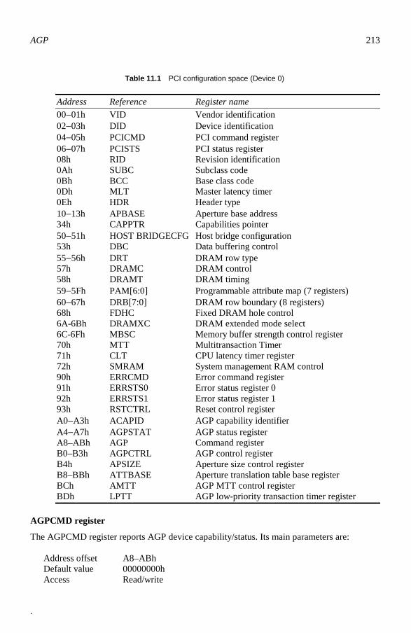
AGP 213
.
Table 11.1 PCI configuration space (Device 0)
Address Reference Register name 00−01h VID Vendor identification 02−03h DID Device identification 04−05h PCICMD PCI command register 06−07h PCISTS PCI status register 08h RID Revision identification 0Ah SUBC Subclass code 0Bh BCC Base class code 0Dh MLT Master latency timer 0Eh HDR Header type 10−13h APBASE Aperture base address 34h CAPPTR Capabilities pointer 50−51h HOST BRIDGECFG Host bridge configuration 53h DBC Data buffering control 55−56h DRT DRAM row type 57h DRAMC DRAM control 58h DRAMT DRAM timing 59−5Fh PAM[6:0] Programmable attribute map (7 registers) 60−67h DRB[7:0] DRAM row boundary (8 registers) 68h FDHC Fixed DRAM hole control 6A-6Bh DRAMXC DRAM extended mode select 6C-6Fh MBSC Memory buffer strength control register 70h MTT Multitransaction Timer 71h CLT CPU latency timer register 72h SMRAM System management RAM control 90h ERRCMD Error command register 91h ERRSTS0 Error status register 0 92h ERRSTS1 Error status register 1 93h RSTCTRL Reset control register A0−A3h ACAPID AGP capability identifier A4−A7h AGPSTAT AGP status register A8–ABh AGP Command register B0–B3h AGPCTRL AGP control register B4h APSIZE Aperture size control register B8–BBh ATTBASE Aperture translation table base register BCh AMTT AGP MTT control register BDh LPTT AGP low-priority transaction timer register
AGPCMD register
The AGPCMD register reports AGP device capability/status. Its main parameters are:
Address offset A8–ABh Default value 00000000h Access Read/write
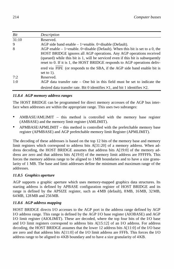
214 Computer busses
Bit Description 31:10 Reserved. 9 AGP side band enable – 1=enable. 0=disable (Default). 8 AGP enable – 1=enable. 0=disable (Default). When this bit is set to a 0, the
HOST BRIDGE ignores all AGP operations. Any AGP operations received (queued) while this bit is 1, will be serviced even if this bit is subsequently reset to 0. If it is 1, the HOST BRIDGE responds to AGP operations deliv-ered via PIPE (or responds to the SBA, if the AGP side band enable bit is set to 1).
7:2 Reserved. 1:0 AGP data transfer rate – One bit in this field must be set to indicate the
desired data transfer rate. Bit 0 identifies ×1, and bit 1 identifies ×2.
11.8.4 AGP memory address ranges
The HOST BRIDGE can be programmed for direct memory accesses of the AGP bus inter-face when addresses are within the appropriate range. This uses two subranges: • AMBASE/AMLIMIT – this method is controlled with the memory base register
(AMBASE) and the memory limit register (AMLIMIT). • APMBASE/APMLIMIT – this method is controlled with the prefetchable memory base
register (APMBASE) and AGP prefetchable memory limit Register (APMLIMIT). The decoding of these addresses is based on the top 12 bits of the memory base and memory limit registers which correspond to address bits A[31:20] of a memory address. When ad-dress decoding, the HOST BRIDGE assumes that address bits A[19:0] of the memory ad-dress are zero and that address bits A[19:0] of the memory limit address are FFFFFh. This forces the memory address range to be aligned to 1 MB boundaries and to have a size granu-larity of 1 MB. The base and limit addresses define the minimum and maximum range of the addresses.
11.8.5 Graphics aperture
AGP supports a graphic aperture which uses memory-mapped graphics data structures. Its starting address is defined by APBASE configuration register of HOST BRIDGE and its range is defined by the APSIZE register, such as 4 MB (default), 8 MB, 16 MB, 32 MB, 64 MB, 128 MB and 256 MB.
11.8.6 AGP address mapping
HOST BRIDGE directs I/O accesses to the AGP port in the address range defined by AGP I/O address range. This range is defined by the AGP I/O base register (AIOBASE) and AGP I/O limit register (AIOLIMIT). These are decoded, where the top four bits of the I/O base and I/O limit registers correspond to address bits A[15:12] of an I/O address. For address decoding, the HOST BRIDGE assumes that the lower 12 address bits A[11:0] of the I/O base are zero and that address bits A[11:0] of the I/O limit address are FFFh. This forces the I/O address range to be aligned to 4 KB boundary and to have a size granularity of 4 KB.

AGP 215
.
11.9 Exercises
11.9.1 Which bus is the AGP bus based on: (a) PCI (b) IDE (c) ISA (d) USB 11.9.2 How does AGP increase the data rate by x2 (and even x4): (a) Extra clock signals (b) Increased data bus size (c) Direct memory accesses (d) Increased address bus size 11.9.3 Which of the following is not an advantage of using the AGP bus: (a) Faster transfers between memory and the graphics devices (b) Increased usage of main memory (with reduced need for localized memory) (c) Reduced requirement for interrupts (d) Increase throughput compared with the standard PCI bus 11.9.4 Which of the following identifies the address/data lines on the AGP bus: (a) HAD[31:0] (b) GAD[31:0] (c) AAD[31:0] (d) AD[31:0] 11.9.5 Explain the main objectives of the AGP bus and outline the advantages of moving
textural information into main memory. 11.9.6 Contrast the PCI and AGP busses and how AGP increases the data throughput.
Also discuss the extra signal lines used with AGP, and how they are used.
11.10 Notes from the author
So, what’s the biggest weakness of the PC. In the past, it has probably been the graphics facilities. This is mainly because the bus systems within the PC did not support large data throughput (ISA/EISA is way too slow). The design of the graphics system also required that the video card required to store all the data which was to be displayed on the screen. Thus no matter the amount of memory on the system, it was still limited by the amount of memory on the graphics card. AGP overcomes this by allowing graphical images to be stored in the main memory and then transferred to the video displayed over a fast bus. The data demand for graphical displays is almost unlimited, as the faster they can be driven, the greater their application. The AGP bus is an excellent extension to the PCI bus, and gives data throughput of over 500 MB/s, whereas standard PCI devices can typically only be run at less than 100 MB/s. AGP is now a standard part of most PC motherboards, and it is still to be seen if many systems will start to use this port.

Fibre Channel
12.1 Introduction
The increase in demand for bandwidth requires faster server-to-storage and server-to-server networking. This is mainly due to the increase in client/server applications. Fibre Channel is one solution to this, as it is a highly reliable technology which operates at gigabit speeds. It interconnects well with other technologies, especially SCSI and TCP/IP. The main applica-tions have been in switches, hubs, storage systems, storage devices and adapters. The term fibre is a generic term which can indicate either optical or a copper cable Its development started in 1988 and ANSI standard approval in 1994. It has the following advantages:
• Cost-effective channel – it is a cost-effective for storage and networks.
• Reliable – it is reliable with assured information delivery.
• Gigabit bitrate – bit rate of 1.06 Gbps, but scalable to 2.12 Gbps and 4.24 Gbps.
• Multiple topologies – it has dedicated point-to-point, shared loops, and scaled switched topologies meet application requirements.
• Multiple protocols – it supports SCSI, TCP/IP, video, or raw data, and is especially suited to real-time video/audio.
• Scalable – it supports single point-to-point gigabit links to integrated enterprises with hundreds of servers.
• Congestion free – data can be sent as fast as the destination buffer can receive it.
• High efficiency – fibre channel has very little transmission overhead.
12.2 Comparison
Fibre channel is designed to support scalable gigabit technology, and provides flow control, self-management, and ultrareliability. It does not suffer from the problems associated with traditional networking technologies. Table 12.1 compares Fibre channel with gigabit ethernet and ATM. In real-time applications, the data must have a guaranteed quality of service. gigabit ethernet does not provide for an assured quality of service, whereas ATM does. Fibre chan-nel improves on ATM as it gives guaranteed delivery, along with gigabit bandwidth, as well as a given quality of service.
12

218 Computer busses
Table 12.1 Comparison between Fibre Channel and other networking technologies
Parameter Fibre channel Gigabit ethernet ATM Technology application Storage, network, video,
clusters
Network Network, video
Topologies Point-to-point loop hub, switched
Point-to-point hub, switched
Switched
Baud rate 1.06 Gbps
1.25 Gbps 622 Mbps
Scalability 2.12 Gbps, 4.24 Gbps
Not defined 1.24 Gbps
Guaranteed delivery Yes
No No
Congestion data loss None
Yes Yes
Frame size Variable, 0–2 KB
Variable, 0–1.5 KB Fixed, 53 B
Flow control Credit based
Rate based Rate based
Physical media Copper/fibre
Copper/fibre Copper/fibre
Protocols supported
Network, SCSI, video Network Network, video
12.3 Fibre channel standards
The ANSI T11 committee developed the X.3230-1994-Fibre channel physical and signaling standard (FC-PH). Its objectives where:
• Performance from 266 Mbps to over 4 Gbps.
• Support for distances up to 10 km.
• Small connectors.
• High-bandwidth utilisation with distance insensitivity.
• Greater connectivity than existing multidrop channels.
• Broad availability using standard components.
• Support for many different system types, from small computers to mainframes.
• Supports multiple existing interface command sets, such as internet protocol (IP), SCSI, IPI, HIPPI-FP and audio/video.
Fibre channel is a channel/network standard which contains networking features to provide for the required connectivity, distance and protocol multiplexing. It also supports traditional channel features for simplicity, repeatable performance, and guaranteed delivery. Fibre chan-nel also works as a generic transport mechanism.

Fibre Channel 219
Fibre channel architecture is based on channel/network integration with an active, intelli-gent interconnection among devices. A port in Fibre channel simply has to manage a simple point-to-point connection. The transmission is isolated from the control protocol, so point-to-point links, arbitrated loops, and switched topologies are used to meet the specific needs of an application. The fabric is self-managing. Nodes do not need station management, which greatly simplifies implementation.
12.4 Cables, hubs, adapters and connectors
Fibre channel uses either fibre optic cables (either multimode or single mode) or four types of copper cables. Normally the copper cables use twin axial with DB-9 or HSSD connectors. Typically, low-cost copper cables are used for short and medium length runs, and fibre optic cable is used for longer lengths. Thus, most hubs and adapters have a standard copper inter-face. For fibre optic cable one of the following is used:
• Multimode cable. This type is used for short distances of up to 22 km. It has a 62.5 µm or 50 µm inner core diameter and allows light to propagate in multiple modes. These modes tend to disperse the signal and thus limits the distance of the cable. Typical band-width ratings for 62.5 µm cable are 200 MHz/km, which gives a range of 200 m at 1 Gbps.
• Single mode cable. This type is used for long cable runs. Its only limitation is the transmitter power and receiver sensitivity. The inner core is 7 µm or 9 µm, which only al-lows a single ray of light to propagate along the cable. There will thus be no dispersion of the signal.
The three main types of connectors used are:
• SC connector. The SC connector is the standard connector for most fibre optic cables and is also used for Fibre Channel. It is basically a push-pull connector and is preferred over the ST screw-on connector.
• Galaxy connector. This is a new type of connector and reduces the size of the connector by 50%, allowing increased connector densities.
There are also various connector/adapter modules, these include:
• Gigabit interface converters (GBIC). These convert a copper cable connector to an optical interface. They use an HSSD connector for the copper interface and media inter-face converters use the DB-9 copper interface.
• Gigabit link modules (GLM). These are pluggable modules which provide either a copper or fibre optic interface, and allow users to easily change the media interface from copper to fibre optics. GLMs include a serialiser-deserialiser (SERDES) and have a me-dia independent parallel interface to the host bus adapter.
• Extenders. These provide for extended cable runs. They typically use multimode cable, and they convert the multimode interface to single-mode, as well as boosting the laser

220 Computer busses
power. For example, an extender can provide a single mode cable distance of 30 km.
• Host bus adapters (HBAs) These are similar to SCSI host bus adapters and network interface cards (NICs) They typically connect directly to the host computer using a stan-dard bus, such as SBus, PCI, MCA, EISA, GIO, HIO, PMC and compact PCI.
• SNA gateway These provide gateways between from Fibre channel to SNA.
• Switch WAN extender These allow the interconnection to WANs using ATM or STM services.
Fibre channel systems can be integrated into virtually any network topology. It can use point-to-point dedicated connection, loop connection (with a shared bandwidth) or switched scaled bandwidth. Fibre channel devices typically either connect to one of the following:
• Hubs. Fibre channel hubs typically connect to a hub using copper cables. These hubs are similar to token ring/FDDI hubs with ‘ring in’ and ‘ring out’, and each port of the hub has an automatic port bypass circuit to automatically open and close the loop. Hubs thus support hot insertion and removal from the loop. If an attached node is not connected or powered on then the hub detects this and bypasses the node. Typically, a hub has 7 to 10 ports and can be stacked to the maximum loop size of 127 ports.
• Switches These allow the simultaneous communication or one or more connections at the same time.
Figure 12.1 shows an example network topology.
Switch
Hub
SCSI RAID
Fibre channel storage system (hot swap)
Point-to- point connection
WAN connection (ATM/STM/FDDI)
Ring network (up to 127 hubs)
Hub
Hub
Workstation cluster
Figure 12.1 Fibre Channel connections

Fibre Channel 221
The networking options include:
• Point-to-point connections – these are point-to-point connections, and are not connected as a ring.
• Switch connections.
• Hub connections – these connect onto a ring, with the ‘ring out’ of each switch con-nected to the ‘ring in’ of the next, and so on. This makes a ring with devices connecting to the hub (and not to the ring).
• Fibre channel storage system – this contains hot swap disks with a 100 MB/s data trans-fer.
• SCSI RAID connection.
• Cluster connection – workstations plug directly to a hub. The hub detects if a work-station is connected and automatically connects it to the ring.
• WAN connection – connection to WAN, such as ATM, STM or FDDI.
12.5 Storage Devices and storage area networks
One of the largest uses of fibre channel is likely to be in storage interfaces. It has many ad-vantages over SCSI, including distance, bandwidth, scalability and reliability. Many manu-facturers now provide RAID-based systems with Fibre channel. A good area of application for Fibre channel is in storage area networks. These typically contain one or more servers, which also connect to one or more storage systems. These stor-age systems could be RAID, tape back-up, CD-ROMs or disk drives. In a fibre channel network, SCSI devices are interfaced to the Fibre channel using a Fibre channel to SCSI bridge, and IP is used for server to server and client/server communications. Fibre channel disks have a back plane with a built-in fibre channel loop. At each disk location in the back-plane loop is a port bypass circuit which permits hot swapping of disks. If a disk is not present, the circuit automatically closes the loop. When a disk is inserted, the loop is opened to connect to the disk.
12.6 Networks
Fibre channel has many advantages over traditional networking technologies, these include:
• Automatic configuration – support for automatic configuration protocols, such as ARP, RARP and other self-discovery protocols.
• Automatic self-discovery of Fibre channel topology.
• Confirmed delivery – this enhances reliability, and does not rely on higher-level proto-cols to confirm delivery.
• Efficient, high-bandwidth low-latency transfers – this uses a variable length frame (up to 2 kB). It uses an efficient protocol which only has an overhead of up to 100 bytes.

222 Computer busses
• Fast connection time – instant circuit setup time using hardware enhanced Fibre channel protocol.
• Guaranteed Quality of Service (QoS) True connection service or fractional bandwidth, connection-oriented virtual circuits to guarantee QoS for critical back-ups or other operations.
• Hybrid topology – Supports many different topologies, such as dedicated point-to-point circuits, shared bandwidth ring networks or scalable bandwidth switched circuits.
• Low latency – extremely low latency connection and connectionless service.
• Real or virtual circuits.
• Synchronous support – this is used with video connections, and uses fractional band-width virtual circuits.
12.7 Exercises
12.7.1 Which of the following offers the highest potential data rate: (a) Single-mode fibre optic (b) Multimode fibre optic (c) Cat-3, shielded twisted pair (d) Cat-5, shielded twisted pair 12.7.2 What is the topology of a large Fibre Channel network: (a) Back plane (b) Bus network (c) Star network (d) Ring network 12.7.3 What devices do workstations normally connect to with a Fibre channel network: (a) Router (b) Hub (c) Bridge (d) Repeater 12.7.4 Which of the following is not an advantage of Fibre channel: (a) High data rate (b) Hot swappable local devices (c) Can be used with many networking protocols (d) Increased amount of ring connections
12.8 Notes from the author
Well, ask any Managing Director of a large commercial organisation about what their key resources is, and, at least, if they are honest, 9 out of 10 of them will say their IT infrastruc-ture. Thus, if a company were to loose electronic mail or their Intranet connections, it would be very costly in lack of efficiency. What is required, then, is a fast and robust network back-bone. This is what fibre channel does best. It’s not cheap, but it’s as good as it gets.

RS-232
13.1 Introduction
RS-232 is one of the most widely used techniques used to interface external equipment to computers. It uses serial communications where one bit is sent along a line, at a time. This differs from parallel communications which send one or more bytes, at a time. The main ad-vantage that serial communications has over parallel communications is that a single wire is needed to transmit and another to receive. RS-232 is a de facto standard that most computer and instrumentation companies comply with. It was standardised in 1962 by the Electronics Industries Association (EIA). Unfortunately this standard only allows short cable runs with low bit rates. The standard RS-232 only allows a bit rate of 19 600 bps for a maximum dis-tance of 20 m. New serial communications standards, such as RS-422 and RS-449, allow very long cable runs and high bit rates. For example, RS-422 allows a bit rate of up to 10 Mbps over distances up to 1 mile, using twisted-pair, coaxial cable or optical fibres. The new standards can also be used to create computer networks. This chapter introduces the RS-232 standard and gives simple programs which can be used to transmit and receive using RS-232.
13.2 Electrical characteristics
13.2.1 Line voltages
The electrical characteristics of RS-232 defines the minimum and maximum voltages of a logic ‘1’ and ‘0’. A logic ‘1’ ranges from –3 V to –25 V, but will typically be around –12 V. A logical ‘0’ ranges from 3 V to 25 V, but will typically be around +12 V. Any voltage be-tween –3 V and +3 V has an indeterminate logical state. If no pulses are present on the line the voltage level is equivalent to a high level, that is –12 V. A voltage level of 0 V at the re-ceiver is interpreted as a line break or a short circuit. Figure 13.1 shows an example trans-mission.
+12V
–12V
1 10 0010Inactive condition
Figure 13.1 RS-232 voltage levels
13

224 Computer busses
13.2.2 DB25S connector
The DB25S connector is a 25-pin D-type connector and gives full RS-232 functionality. Fig-ure 13.2 shows the pin number assignment. A DCE (the terminating cable) connector has a male outer casing with female connection pins. The DTE (the computer) has a female outer casing with male connecting pins. There are three main signal types: control, data and ground. Table 13.1 lists the main connections. Control lines are active HIGH, that is they are HIGH when the signal is active and LOW when inactive.
113
14
23456789101112
1516171819202122232425
Pin Signal2 TxData3 RxData4 RTS5 CTS6 DSR7 GND20 DTR
Figure 13.2 RS-232 DB25S connector
13.2.3 DB9S Connector
The 25-pin connector is the standard for RS-232 connections but as electronic equipment becomes smaller, there is a need for smaller connectors. For this purpose most PCs now use a reduced function 9-pin D-type connector rather than the full function 25-way D-type. As with the 25-pin connector the DCE (the terminating cable) connector has a male outer casing with female connection pins. The DTE (the computer) has a female outer casing with male connecting pins. Figure 13.3 shows the main connections.
1
6
2345
789
Pin Signal2 RxData3 TxData4 DTR5 GND6 DSR7 RTS8 CTS
Figure 13.3 RS-232 DB9S interface
13.2.4 PC connectors
All PCs have at least one serial communications port. The primary port is named COM1: and the secondary is COM2:. There are two types of connectors used in RS-232 communications, these are the 25- and 9-way D-type. Most modern PCs use either a 9-pin connector for the primary (COM1:) serial port and a 25-pin for a secondary serial port (COM2:), or they use two 9-pin connectors for serial ports. The serial port can be differentiated from the parallel port in that the 25-pin parallel port (LPT1:) is a 25-pin female connector on the PC and a male connector on the cable. The 25-pin serial connector is a male on the PC and a female on the cable. The different connector types can cause problems in connecting devices. Thus a 25-to-9 pin adapter is a useful attachment, especially to connect a serial mouse to a 25-pin connector.

RS-232 225
Table 13.1 Main pin connections used in 25-pin connector
Pin Name Abbreviation Functionality 1 Frame ground FG This ground normally connects the outer sheath of the
cable and to earth ground.
2 Transmit data TD Data is sent from the DTE (computer or terminal) to a DCE via TD.
3 Receive data RD Data is sent from the DCE to a DTE (computer or ter-minal) via RD.
4 Request to send RTS DTE sets this active when it is ready to transmit data.
5 Clear to send CTS DCE sets this active to inform the DTE that it is ready to receive data.
6 Data set ready DSR Similar functionality to CTS but activated by the DTE when it is ready to receive data.
7 Signal ground SG All signals are referenced to the signal ground (GND).
20 Data terminal ready
DTR Similar functionality to RTS but activated by the DCE when it wishes to transmit data.
13.2.5 Frame format
RS-232 uses asynchronous communication which has a start/stop data format (Figure 13.4). Each character is transmitted one at a time with a delay between them. This delay is called the inactive time and is set at a logic level high (–12 V) as shown in Figure 13.5. The trans-mitter sends a start bit to inform the receiver that a character is to be sent in the following bit transmission. This start bit is always a ‘0’. Next, 5, 6 or 7 data bits are sent as a 7-bit ASCII character, followed by a parity bit and finally either 1, 1.5 or 2 stop bits. Figure 13.5 shows a frame format and an example transmission of the character ‘A’, using odd parity. The timing of a single bit sets the rate of transmission. Both the transmitter and receiver need to be set to the same bit-time interval. An internal clock on both sets this interval. These only have to be roughly synchronised at approximately the same rate as data is transmitted in relatively short bursts.
Tx Character Tx Character Tx Character
Inactive condition
Figure 13.4 Asynchronous communications

226 Computer busses
0 b 0 b 1 P S1 S2 1
start bit ASCII
character Parity bit Stop
bit(s)
0 1 0 0 0 0 0 1 1 1 1
‘A’ (100 0001)
b 2 b 3 b 4 b 5 b 6
Figure 13.5 RS-232 frame format
Example An RS-232 serial data link uses 1 start bit, 7 data bits, 1 parity bit, 2 stop bits, ASCII coding and even parity. Determine the message sent from the following bit stream. First bit sent ⇓ 1111101000001011000001111111111111100000111111110001100111101010 0111111111111 Answer The format of the data string sent is given next: idle 11111 start bit 0 ‘A’ 1000001 parity bit 0 stop bits 11 start bit 0 ‘p’ 0000111 parity bit 1 stop bits 11 idle 11111111 start bit 0 ‘p’ 0000111 parity bit 1 stop bits 11 idle 11 start bit 0 ‘L’ 0011001 parity bit 1 stop bits 11 The message sent was thus ‘AppL’.
Parity
Error control is data added to transmitted data in order to detect or correct an error in trans-mission. RS-232 uses a simple technique known as parity to provide a degree of error detec-tion. A parity bit is added to transmitted data to make the number of 1s sent either even (even parity) or odd (odd parity). It is a simple method of error coding and only requires exclusive-OR (XOR) gates to generate the parity bit. The parity bit is added to the transmitted data by
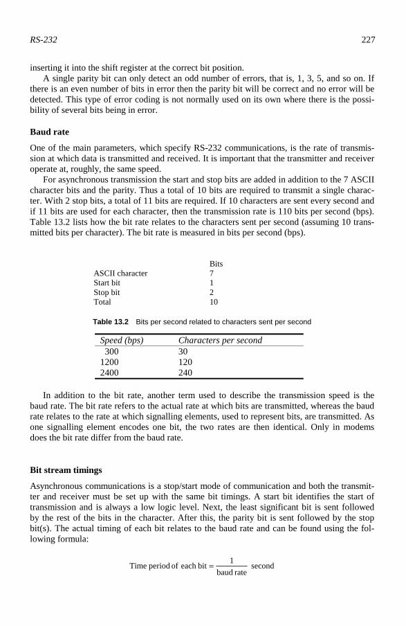
RS-232 227
inserting it into the shift register at the correct bit position. A single parity bit can only detect an odd number of errors, that is, 1, 3, 5, and so on. If there is an even number of bits in error then the parity bit will be correct and no error will be detected. This type of error coding is not normally used on its own where there is the possi-bility of several bits being in error.
Baud rate
One of the main parameters, which specify RS-232 communications, is the rate of transmis-sion at which data is transmitted and received. It is important that the transmitter and receiver operate at, roughly, the same speed. For asynchronous transmission the start and stop bits are added in addition to the 7 ASCII character bits and the parity. Thus a total of 10 bits are required to transmit a single charac-ter. With 2 stop bits, a total of 11 bits are required. If 10 characters are sent every second and if 11 bits are used for each character, then the transmission rate is 110 bits per second (bps). Table 13.2 lists how the bit rate relates to the characters sent per second (assuming 10 trans-mitted bits per character). The bit rate is measured in bits per second (bps).
Bits ASCII character 7 Start bit 1 Stop bit 2 Total 10
Table 13.2 Bits per second related to characters sent per second
Speed (bps) Characters per second 300 30 1200 120 2400 240
In addition to the bit rate, another term used to describe the transmission speed is the baud rate. The bit rate refers to the actual rate at which bits are transmitted, whereas the baud rate relates to the rate at which signalling elements, used to represent bits, are transmitted. As one signalling element encodes one bit, the two rates are then identical. Only in modems does the bit rate differ from the baud rate.
Bit stream timings
Asynchronous communications is a stop/start mode of communication and both the transmit-ter and receiver must be set up with the same bit timings. A start bit identifies the start of transmission and is always a low logic level. Next, the least significant bit is sent followed by the rest of the bits in the character. After this, the parity bit is sent followed by the stop bit(s). The actual timing of each bit relates to the baud rate and can be found using the fol-lowing formula:
second rate baud
1biteach of period Time =

228 Computer busses
For example, if the baud rate is 9600 baud (or bps) then the time period for each bit sent is 1/9600 s or 104 µs. Table 13.3 shows some bit timings as related to baud rate. An example of the voltage levels and timings for the ASCII character ‘V’ is given in Figure 13.6.
Table 13.3 Bit timings related to baud rate
Baud rate Time for each bit (µs) 1 200 833 2 400 417 9 600 104 19 200 52
Start
bit0 1 1 0 1 0 1
Stop
bit
ASCII ‘V’ 101 0110
Baud rate: 9600 baud
+12 V
-12 V
Figure 13.6 ASCII ‘V’ at RS-232 voltage levels
13.3 Communications between two nodes
RS-232 is intended to be a standard but not all manufacturers abide by it. Some implement the full specification while others implement just a partial specification. This is mainly be-cause not every device requires the full functionality of RS-232, for example a modem re-quires many more control lines than a serial mouse. The rate at which data is transmitted and the speed at which the transmitter and receiver can transmit/receive the data dictates whether data handshaking is required.
13.3.1 Handshaking
In the transmission of data, there can either be no handshaking, hardware handshaking or software handshaking. If no handshaking is used then the receiver must be able to read the received characters before the transmitter sends another. The receiver may buffer the re-ceived character and store it in a special memory location before it is read. This memory lo-cation is named the receiver buffer. Typically, it may only hold a single character. If it is not emptied before another character is received then any character previously in the buffer will be overwritten. An example of this is illustrated in Figure 13.6. In this case, the receiver has read the first two characters successfully from the receiver buffer, but it did not read the third character as the fourth transmitted character has overwritten it in the receiver buffer. If this condition occurs then some form of handshaking must be used to stop the transmitter sending characters before the receiver has had time to service the received characters. Hardware handshaking involves the transmitter asking the receiver if it is ready to receive
120 µS

RS-232 229
data. If the receiver buffer is empty it will inform the transmitter that it is ready to receive data. Once the data is transmitted and loaded into the receiver buffer the transmitter is in-formed not to transmit any more characters until the character in the receiver buffer has been read. The main hardware handshaking lines used for this purpose are:
• CTS – Clear to send. • RTS – Ready to send. • DTR – Data terminal ready. • DSR – Data set ready.
Software handshaking involves sending special control characters. These include the DC1 (Xon)-DC4 (Xoff) control characters.
Transmitter Receiver
Receiverreads frombuffer
receiverbuffer
transmittedcharacters
transmitterbuffer
Receiver hasfailed to read thebuffer before anothercharacter has beenreceived
Figure 13.7 Transmission and reception of characters
13.3.2 RS-232 set-up
Microsoft Windows allows the serial port setting to be set by selecting control panel → sys-tem → device manager → ports (COM and LPT) → port settings. The settings of the com-munications port (the IRQ and the port address) can be changed by selecting control panel → system → device manager → ports (COM and LPT) → resources for IRQ and addresses. Figure 13.8 shows example parameters and settings. The selectable baud rates are typically 110, 300, 600, 1200, 2400, 4800, 9600 and 19 200 baud for an 8250-based device. A 16650 UART also gives enhanced speeds of 38 400, 57 600, 115 200, 230 400, 460 800 and 921 600 baud. Notice that the flow control can either be set to software handshaking (Xon/Xoff), hardware handshaking or none. The parity bit can either be set to none, odd, even, mark or space. A mark in the parity option sets the parity bit to a ‘1’ and a space sets it to a ‘0’. In this case COM1: is set at 9600 baud, 8 data bits, no parity, 1 stop bit and no parity checking.

230 Computer busses
Figure 13.8 Changing port setting and parameters
13.3.3 Simple no-handshaking communications
In this form of communication it is assumed that the receiver can read the received data from the receive buffer before another character is received. Data is sent from a TD pin connection of the transmitter and is received in the RD pin connection at the receiver. When a DTE (such as a computer) connects to another DTE, then the transmit line (TD) on one is con-nected to the receive (RD) of the other and vice versa. Figure 13.9 shows the connections between the nodes.
TD
RD
RTS
CTS
DTR
DSR
GND
TD
RD
RTS
CTS
DTR
DSR
GND
3
2
7
8
4
6
5
3
2
7
8
4
6
5
9-pin 9-pin
TD
RD
RTS
CTS
DTR
DSR
GND
TD
RD
RTS
CTS
DTR
DSR
GND
3
2
7
8
4
6
5
2
3
4
5
20
6
7
9-pin 25-pin
Figure 13.9 RS-232 connections with no hardware handshaking
13.3.4 Software handshaking
There are two ASCII characters that start and stop communications. These are X-ON (^S , Cntrl-S or ASCII 11) and X-OFF (^Q, Cntrl-Q or ASCII 13). When the transmitter receives an X-OFF character it ceases communications until an X-ON character is sent. This type of handshaking is normally used when the transmitter and receiver can process data relatively

RS-232 231
quickly. Normally, the receiver will also have a large buffer for the incoming characters. When this buffer is full, it transmits an X-OFF. After it has read from the buffer the X-ON is transmitted, see Figure 13.10.
X-OFF
X-ON
Tran
smitt
er
Datatransmission
Datatransmission
Rec
eive
r
Figure 13.10 Software handshaking using X-ON and X-OFF
13.3.5 Hardware handshaking
Hardware handshaking stops characters in the receiver buffer from being overwritten. The control lines used are all active HIGH. Figure 13.11 shows how the nodes communicate. When a node wishes to transmit data it asserts the RTS line active (that is, HIGH). It then monitors the CTS line until it goes active (that is, HIGH). If the CTS line at the transmitter stays inactive then the receiver is busy and cannot receive data, at the present. When the re-ceiver reads from its buffer the RTS line will automatically go active indicating to the trans-mitter that it is now ready to receive a character.
Are you readyto receive ?
NoCTS
RTS
YesCTS
TD
Send character
Transmitting node
CTS
RTS
RD
RTS
Receiving node
Figure 13.11 Handshaking lines used in transmitting data

232 Computer busses
Receiving data is similar to the transmission of data, but the lines DSR and DTR are used instead of RTS and CTS. When the DCE wishes to transmit to the DTE the DSR input to the receiver will become active. If the receiver cannot receive the character, it will set the DTR line inactive. When it is clear to receive it sets the DTR line active and the remote node then transmits the character. The DTR line will be set inactive until the character has been proc-essed.
13.3.6 Two-way communications with handshaking
For full handshaking of the data between two nodes the RTS and CTS lines are crossed over (as are the DTR and DSR lines). This allows for full remote node feedback (see Figure 13.12).
DTE DTE
RTS
CTS
DTR
DSR
GND
TD
RD
RTS
CTS
DTR
DSR
GND
3
7
8
4
6
5
3TD
RD 2 2
7
8
4
6
5
3
2
7
8
4
6
5
2
3
4
5
20
6
7
9-pin 9-pin 9-pin 25-pin
DTE DTE
TD
RD
RTS
CTS
DTR
DSR
GND
TD
RD
RTS
CTS
DTR
DSR
GND
Figure 13.12 RS-232 communications with handshaking
13.3.7 DTE-DCE connections (PC to modem)
A further problem occurs in connecting two nodes. A DTE/DTE connection requires cross-overs on their signal lines, whereas DTE/DCE connections require straight-through lines. An example computer to modem connection is shown in Figure 13.13.
3
7
8
4
6
5
2
2
4
5
20
6
7
3
3
7
8
4
6
5
2
3
7
8
4
6
5
2
DTE DCE
RTS
CTS
DTR
DSR
GND
TD
RD
9-pin 9-pin 9-pin 25-pin
DTE DCE
RTS
CTS
DTR
DSR
GND
TD
RD
RTS
CTS
DTR
DSR
GND
TD
RD
RTS
CTS
DTR
DSR
GND
TD
RD
Figure 13.13 DTE to DCE connections
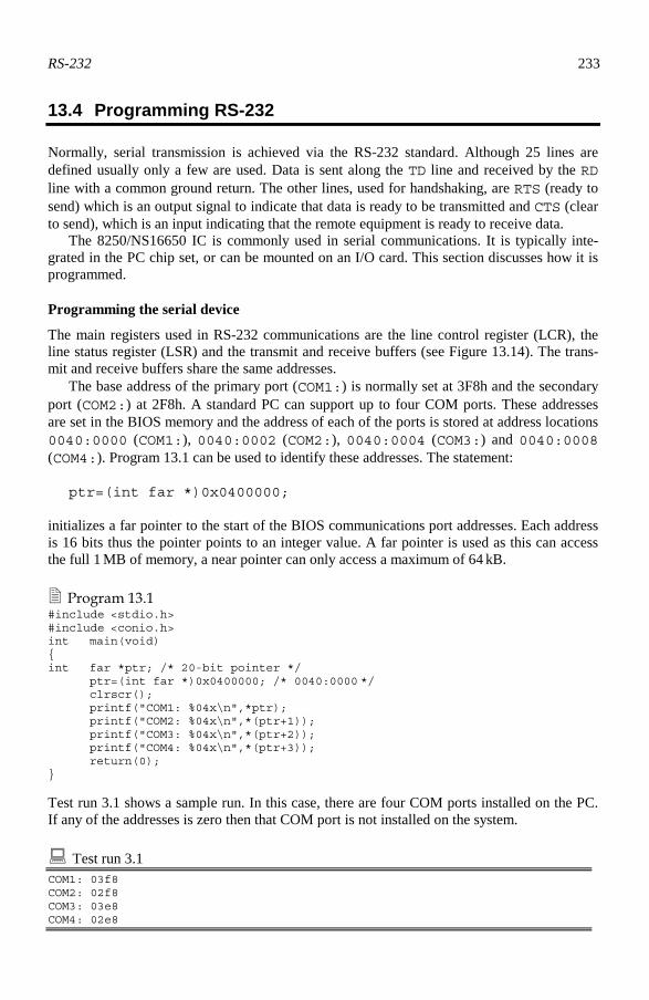
RS-232 233
13.4 Programming RS-232
Normally, serial transmission is achieved via the RS-232 standard. Although 25 lines are defined usually only a few are used. Data is sent along the TD line and received by the RD line with a common ground return. The other lines, used for handshaking, are RTS (ready to send) which is an output signal to indicate that data is ready to be transmitted and CTS (clear to send), which is an input indicating that the remote equipment is ready to receive data. The 8250/NS16650 IC is commonly used in serial communications. It is typically inte-grated in the PC chip set, or can be mounted on an I/O card. This section discusses how it is programmed.
Programming the serial device
The main registers used in RS-232 communications are the line control register (LCR), the line status register (LSR) and the transmit and receive buffers (see Figure 13.14). The trans-mit and receive buffers share the same addresses. The base address of the primary port (COM1:) is normally set at 3F8h and the secondary port (COM2:) at 2F8h. A standard PC can support up to four COM ports. These addresses are set in the BIOS memory and the address of each of the ports is stored at address locations 0040:0000 (COM1:), 0040:0002 (COM2:), 0040:0004 (COM3:) and 0040:0008 (COM4:). Program 13.1 can be used to identify these addresses. The statement: ptr=(int far *)0x0400000; initializes a far pointer to the start of the BIOS communications port addresses. Each address is 16 bits thus the pointer points to an integer value. A far pointer is used as this can access the full 1 MB of memory, a near pointer can only access a maximum of 64 kB.
Program 13.1 #include <stdio.h> #include <conio.h> int main(void) int far *ptr; /* 20-bit pointer */ ptr=(int far *)0x0400000; /* 0040:0000 */ clrscr(); printf("COM1: %04x\n",*ptr); printf("COM2: %04x\n",*(ptr+1)); printf("COM3: %04x\n",*(ptr+2)); printf("COM4: %04x\n",*(ptr+3)); return(0);
Test run 3.1 shows a sample run. In this case, there are four COM ports installed on the PC. If any of the addresses is zero then that COM port is not installed on the system.
Test run 3.1 COM1: 03f8 COM2: 02f8 COM3: 03e8 COM4: 02e8
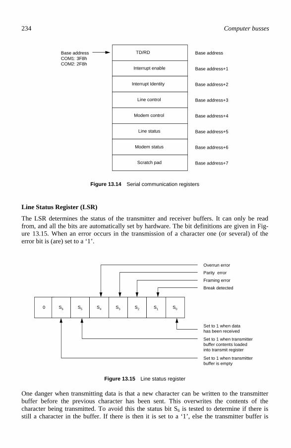
234 Computer busses
TD/RD Base address
Interrupt enable Base address+1
Interrupt Identity Base address+2
Line control Base address+3
Modem control Base address+4
Line status Base address+5
Modem status Base address+6
Scratch pad Base address+7
Base address COM1: 3F8h COM2: 2F8h
Figure 13.14 Serial communication registers
Line Status Register (LSR)
The LSR determines the status of the transmitter and receiver buffers. It can only be read from, and all the bits are automatically set by hardware. The bit definitions are given in Fig-ure 13.15. When an error occurs in the transmission of a character one (or several) of the error bit is (are) set to a ‘1’.
0 S6 S5 S4 S3 S2 S1 S0
Set to 1 when datahas been received
Set to 1 when transmitterbuffer contents loadedinto transmit register
Set to 1 when transmitterbuffer is empty
Overrun error
Parity error
Framing error
Break detected
Figure 13.15 Line status register
One danger when transmitting data is that a new character can be written to the transmitter buffer before the previous character has been sent. This overwrites the contents of the character being transmitted. To avoid this the status bit S6 is tested to determine if there is still a character in the buffer. If there is then it is set to a ‘1’, else the transmitter buffer is

RS-232 235
character in the buffer. If there is then it is set to a ‘1’, else the transmitter buffer is empty. To send a character Test bit 6 until set; Send character; A typical Pascal routine is repeat status := port[LSR] and $40; until (status=$40);
When receiving data the S0 bit is tested to determine if there is a bit in the receiver buffer. To receive a character Test bit 0 until set; Read character; A typical Pascal routine is repeat status := port[LSR] and $01; until (status=$01);
Figure 13.16 shows how the LSR is tested for the transmission and reception of characters.
Line control register (LCR)
The LCR sets up the communications parameters. These include the number of bits per char-acter, the parity and the number of stop bits. It can be written to or read from and has a simi-lar function to that of the control registers used in the PPI (programmable parallel interface) and PTC (programmable timer/counter). The bit definitions are given in Figure 13.17.
TX buffer RX buffer
Character to betransmitted
Characterreceived
1
Transmitter Receiver
1
LSR
LSR
Test S0 to determine if the RX buffer is full
Test S6 to determine ifthe TX buffer is empty
Figure 13.16 Testing of the LSR for the transmission and reception of characters
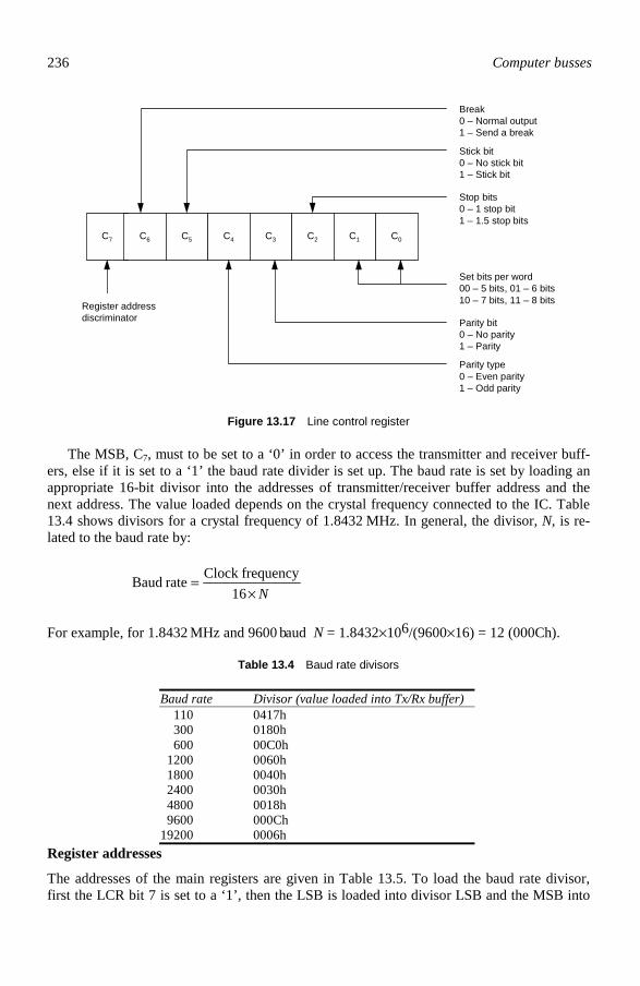
236 Computer busses
C7 C6 C5 C4 C3 C2 C1 C0
Set bits per word00 – 5 bits, 01 – 6 bits10 – 7 bits, 11 – 8 bits
Parity bit0 – No parity1 – Parity
Parity type0 – Even parity1 – Odd parity
Break0 – Normal output1 – Send a break
Stick bit0 – No stick bit1 – Stick bit
Stop bits0 – 1 stop bit1 – 1.5 stop bits
Register addressdiscriminator
Figure 13.17 Line control register
The MSB, C7, must to be set to a ‘0’ in order to access the transmitter and receiver buff-ers, else if it is set to a ‘1’ the baud rate divider is set up. The baud rate is set by loading an appropriate 16-bit divisor into the addresses of transmitter/receiver buffer address and the next address. The value loaded depends on the crystal frequency connected to the IC. Table 13.4 shows divisors for a crystal frequency of 1.8432 MHz. In general, the divisor, N, is re-lated to the baud rate by:
N×
=16
frequencyClock rate Baud
For example, for 1.8432 MHz and 9600 baud N = 1.8432×10⁶/(9600×16) = 12 (000Ch).
Table 13.4 Baud rate divisors
Register addresses
The addresses of the main registers are given in Table 13.5. To load the baud rate divisor, first the LCR bit 7 is set to a ‘1’, then the LSB is loaded into divisor LSB and the MSB into
Baud rate Divisor (value loaded into Tx/Rx buffer) 110 300 600 1200 1800 2400 4800 9600 19200
0417h 0180h 00C0h 0060h 0040h 0030h 0018h 000Ch 0006h

RS-232 237
the divisor MSB register. Finally, bit 7 is set back to a ‘0’. For example, for 9600 baud, COM1 and 1.8432 MHz clock then 0Ch is loaded in 3F8h and 00h into 3F9h. When bit 7 is set at a ‘0’ then a read from the base address reads from the RD buffer and a write operation writes to the TD buffer. An example of this is shown in Figure 13.9.
TD bufferTD3F8h
Write to TD/RDbuffer
RD bufferRD3F8hRead from TD/RD
buffer
Figure 13.18 Read and write from TD/RD buffer
Table 13.5 Serial communications addresses
Primary Secondary Register Bit 7 of LCR 3F8h 2F8h TD buffer ‘0’ 3F8h 2F8h RD buffer ‘0’ 3F8h 2F8h Divisor LSB ‘1’ 3F9h 2F9h Divisor MSB ‘1’ 3FBh 2FBh Line Control Register 3FDh 2FDh Line Status Register
13.5 RS-232 programs
Figure 13.19 shows the main RS-232 connections for 9 and 25-pin connections without hardware handshaking. The loopback connections are used to test the RS-232 hardware and the software, while the null modem connections are used to transmit characters between two computers. Program 13.2 uses a loop back on the TD/RD lines so that a character sent by the computer will automatically be received into the receiver buffer. This set-up is useful in test-ing the transmit and receive routines. The character to be sent is entered via the keyboard. A CNTRL-D (^D) keystroke exits the program. Program 13.3 can be used as a sender program (send.c) and Program 13.4 can be used as a receiver program (receive.c). With these programs, the null modem connections shown in Figure 13.19 are used. Note that programs 13.2 to 13.4 are written for Microsoft Visual C++. For early versions of Borland C/C++ program change _inp for inportb and _outp for outportb.

238 Computer busses
RD
TD
GND
2
3
9-pin D-typeconnector(loopback)
RD
TD
GND
2
3
9-pin D-typeconnector(loopback)
RD
TD
GND
2
9-pin D-typeto 9-pin connection(null modem withouthandshaking)
RD
TD
GND
3
5
2
3
5
TD
RD
GND
2
25-pin D-typeto 25-pin connection(null modem withouthandshaking)
TD
RD
GND
3
7
2
3
7
RD
TD
GND
2
9-pin D-typeto 25-pin connection(null modem withouthandshaking)
TD
TD
GND
3
5
2
3
7
Figure 13.19 System connections
Program 13.2 /* This program transmits a character from COM1: and receives */ /* it via this port. The TD is connected to RD. */ #define COM1BASE 0x3F8 #define COM2BASE 0x2F8 #define TXDATA COM1BASE #define LCR (COM1BASE+3) /* 0x3FB line control */ #define LSR (COM1BASE+5) /* 0x3FD line status */ #include <conio.h> /* required for getch() */ #include <dos.h> /* */ #include <stdio.h> /* Some ANSI C prototype definitions */ void setup_serial(void); void send_character(int ch); int get_character(void); int main(void) int inchar,outchar; setup_serial(); do puts("Enter char to be transmitted (Cntrl-D to end)"); outchar=getch(); send_character(outchar); inchar=get_character(); printf("Character received was %c\n",inchar); while (outchar!=4); return(0); void setup_serial(void)

RS-232 239
_outp( LCR, 0x80); /* set up bit 7 to a 1 to set Register address bit */ _outp(TXDATA,0x0C); _outp(TXDATA+1,0x00); /* load TxRegister with 12, crystal frequency is 1.8432MHz */ _outp(LCR, 0x0A); /* Bit pattern loaded is 00001010b, from msb to lsb these are: */ /* 0 - access TD/RD buffer , 0 - normal output */ /* 0 - no stick bit , 0 - even parity */ /* 1 - parity on, 0 - 1 stop bit */ /* 10 - 7 data bits */ void send_character(int ch) char status; do status = _inp(LSR) & 0x40; while (status!=0x40); /*repeat until Tx buffer empty ie bit 6 set*/ _outp(TXDATA,(char) ch); int get_character(void) int status; do status = _inp(LSR) & 0x01; while (status!=0x01); /* Repeat until bit 1 in LSR is set */ return( (int)_inp(TXDATA));
Program 13.3
/* send.c */ #define TXDATA 0x3F8 #define LSR 0x3FD #define LCR 0x3FB #include <stdio.h> #include <conio.h> /* included for getch */ #include <dos.h> void setup_serial(void); void send_character(int ch); int main(void) int ch; puts("Transmitter program. Please enter text (Cntl-D to end)"); setup_serial(); do ch=getche(); send_character(ch);
240 Computer busses
while (ch!=4); return(0); void setup_serial(void) _outp( LCR, 0x80); /* set up bit 7 to a 1 to set Register address bit */ _outp(TXDATA,0x0C); _outp(TXDATA+1,0x00); /* load TxRegister with 12, crystal frequency is 1.8432MHz */ _outp(LCR, 0x0A); /* Bit pattern loaded is 00001010b, from msb to lsb these are: */ /* Access TD/RD buffer, normal output, no stick bit */ /* even parity, parity on, 1 stop bit, 7 data bits */ void send_character(int ch) char status; do status = _inp(LSR) & 0x40; while (status!=0x40); /*repeat until Tx buffer empty ie bit 6 set*/ _outp(TXDATA,(char) ch);
Program 13.4
/* receive.c */ #define TXDATA 0x3F8 #define LSR 0x3FD #define LCR 0x3FB #include <stdio.h> #include <conio.h> /* included for getch */ #include <dos.h> void setup_serial(void); int get_character(void); int main(void) int inchar; setup_serial(); do inchar=get_character(); putchar(inchar); while (inchar!=4); return(0); void setup_serial(void) _outp( LCR, 0x80); /* set up bit 7 to a 1 to set Register address bit */ _outp(TXDATA,0x0C); _outp(TXDATA+1,0x00); /* load TxRegister with 12, crystal frequency is 1.8432MHz */ _outp(LCR, 0x0A); /* Bit pattern loaded is 00001010b, from msb to lsb these are: */ /* Access TD/RD buffer, normal output, no stick bit */ /* even parity, parity on, 1 stop bit, 7 data bits */

RS-232 241
int get_character(void) int status; do status = _inp(LSR) & 0x01; while (status!=0x01); /* Repeat until bit 1 in LSR is set */ return( (int)_inp(TXDATA));
13.6 Exercises
13.6.1 Which is the maximum cable length for a standard RS-232 connection: (a) 2 m (b) 2 0m (c) 200 m (d) 2 km 13.6.2 Which enhancement to RS-232 allows for 1Mbps bit rates and increased cable
lengths: (a) RS-232x (b) RS-422 (c) RS-444 (d) RS-233 13.6.3 Which of the following is not a standard RS-232 bit rate: (a) 110 bps (b) 4800 bps (c) 9600 bps (d) 12 200 bps 13.6.4 Which voltage range is used for a ‘0’ bit value: (a) –3 V to –25 V (b) 0 V to –3 V (c) +3 V to +25 V (d) 0 V to +3 V 13.6.5 In RS-232, how is the inactive period identified: (a) A high voltage level (b) A low voltage level (c) Zero voltage level (d) Open circuit 13.6.6 How is a null modem cable identified: (a) Direct connection between all the signal lines (b) No connections to TD and RD lines (c) Cross-over between the TD and RD, and handshaking lines (d) No hardware handshaking lines 13.6.7 How is a modem cable identified: (a) Direct connection between all the signal lines

242 Computer busses
(b) No connections to TD and RD lines (c) Cross-over between the TD and RD, and handshaking lines (d) No hardware handshaking lines 13.6.8 The main connections used to transmit data over a null modem cable with no
hardware handshaking are: (a) TD, RD, GND (b) RTS, CTS, GND (c) DSR, DTR, GND (d) TD, RD, RTS, CTS 13.6.9 If a device transmits at 9600 bps, approximately how many characters are
transmitted every minute: (a) 5760 (b) 57600 (c) 576000 (d) 5760000 13.6.10 If a device transmits at 4800 bps, approximately what is the period of a single bit: (a) 2.08µs (b) 20.8µs (c) 208µs (d) 2.08 ms 13.6.11 Which handshaking line is used by a transmitter to identify that it is read to send
data: (a) RTS (b) CTS (c) DTR (d) DTE 13.6.12 Which handshaking line is used by a receiver to identify that it is ready to receive
data: (a) RTS (b) CTS (c) DTR (d) DTE 13.6.13 Which characters are used to start and stop data transfer in software handshaking: (a) X-ON, X-OFF (b) OFF, ON (c) IN, OUT (d) LF, CR 13.6.14 Which is the standard I/O port address for COM1: (a) 1F8h (b) 2F8h (c) 3F8h (d) 4F8h 13.6.15 Which is the standard I/O port address for COM2: (a) 1F8h (b) 2F8h (c) 3F8h (d) 4F8h 13.6.16 The standard IC used in RS-232 communications is:

RS-232 243
(a) 8232 (b) 8086 (c) 8088 (d) 8250 13.6.17 Which register is used to determine the status of the RS-232 connection: (a) LSR (b) LCR (c) STATUS (d) TD/RD buffer 13.6.18 Which register is used to configure the RS-232 connection: (a) LSR (b) LCR (c) STATUS (d) TD/RD buffer 13.6.19 Write a program that continuously sends the character ‘A’ to the serial line. Ob-
serve the output on an oscilloscope and identify the bit pattern and the baud rate. 13.6.20 Write a program that continuously sends the characters from ‘A’ to ‘Z’ to the se-
rial line. Observe the output on an oscilloscope. 13.6.21 Modify Program 13.2 so that the program prompts the user for the baud rate when
the program is started. A sample run is shown in Sample run 13.1.
Sample run 13.1 Enter baud rate required: 1 110 2 150 3 300 4 600 5 1200 6 2400 7 4800 8 9600 >> 8 RS232 transmission set to 9600 baud
13.6.22 Complete Table 13.6 to give the actual time to send 1000 characters for the given
baud rates. Compare these values with estimated values. Note that approximately 10 bits are used for each character thus 960 characters
per second will be transmitted at 9600 baud.
Table 13.6 Baud rate divisors
Baud rate
Time to send 1000 characters (s)
110 300 600 1200 2400 4800 9600 19200
13.6.23 Modify the setup_serial() routine so that the RS232 parameters can be passed to it. These parameters should include the comport (either COM1: or COM2:), the

244 Computer busses
baud rate, the number of data bits and the type of parity. An outline of the modi-fied function is given in Program 13.5.
Program 13.5 #define COM1BASE 0x3F8 #define COM2BASE 0x2F8 #define COM1 0 #define COM2 1 enum baud_rates BAUD110,BAUD300,BAUD600,BAUD1200, BAUD2400,BAUD4800,BAUD9600; enum parity NO_PARITY,EVEN_PARITY,ODD_PARITY; enum databits DATABITS7,DATABITS8; #include <conio.h> #include <dos.h> #include <stdio.h> void setup_serial(int comport, int baudrate, int parity, int databits); void send_character(int ch); int get_character(void); int main(void) int inchar,outchar; setup_serial(COM1,BAUD2400,EVEN_PARITY,DATABITS7); :::::::::::etc. void setup_serial(int comport, int baudrate, int parity, int databits) int tdreg,lcr; if (comport==COM1) tdreg=COM1BASE; lcr=COM1BASE+3; else tdreg=COM2BASE; lcr=COM2BASE+3; _outp( lcr, 0x80); /* set up bit 7 to a 1 to set Register address bit */ switch(baudrate) case BAUD110: _outp(tdreg,0x17);_outp(tdreg+1,0x04); break; case BAUD300: _outp(tdreg,0x80);_outp(tdreg+1,0x01); break; case BAUD600: _outp(tdreg,0x00);_outp(tdreg+1,0xC0); break; case BAUD1200: _outp(tdreg,0x00);_outp(tdreg+1,0x40);break; case BAUD2400: _outp(tdreg,0x00);_outp(tdreg+1,0x30);break; case BAUD4800: _outp(tdreg,0x00);_outp(tdreg+1,0x18);break; case BAUD9600: _outp(tdreg,0x00);_outp(tdreg+1,0x0C);break; :::::::::: etc.
13.6.24 One problem with Programs 13.2 and 13.3 is that when the return key is pressed
only one character is sent. The received character will be a carriage return which returns the cursor back to the start of a line and not to the next line. Modify the re-ceiver program so that a line feed will be generated automatically when a carriage return is received. Note a carriage return is an ASCII 13 and line feed is a 10.

RS-232 245
13.6.25 Modify the get_character() routine so that it returns an error flag if it detects an error or if there is a time-out. Table 13.7 lists the error flags and the returned error value. An outline of the C code is given in Program 13.6. If a character is not re-ceived within 10 s an error message should be displayed.
Table 13.7 Error returns from get_character().
Error condition Error flag return
Notes
Parity error –1 Overrun error –2 Framing error –3 Break detected –4 Time out –5 get_character() should time out if no
characters are received with 10 seconds. Test the routine by connecting two PCs together and set the transmitter with dif-
fering RS-232 parameters.
Program 13.6 #include <stdio.h> #include <dos.h> #define TXDATA 0x3F8 #define LSR 0x3FD #define LCR 0x3FB void show_error(int ch); int get_character(void); enum RS232_errors PARITY_ERROR=-1, OVERRUN_ERROR=-2, FRAMING_ERROR=-3, BREAK_DETECTED=-4, TIME_OUT=-5; int main(void) int inchar; do inchar=get_character(); if (inchar<0) show_error(inchar); else printf("%c",inchar); while (inchar!=4); return(0); void show_error(int ch) switch(ch) case PARITY_ERROR: printf("Error: Parity error/n"); break; case OVERRUN_ERROR: printf("Error: Overrun error/n"); break; case FRAMING_ERROR: printf("Error: Framing error/n"); break; case BREAK_DETECTED: printf("Error: Break detected/n");break; case TIME_OUT: printf("Error: Time out/n"); break; int get_character(void) int instatus; do instatus = _inp(LSR) & 0x01;

246 Computer busses
if (instatus & 0x02) return(BREAK_DETECTED); :::: etc while (instatus!=0x01 ); return( (int) _inp(TXDATA) );
13.7 Notes from the author
Good old RS-232. My bank manager would certainly agree with this, as I have made more consultancy income with it than any other piece of computer equipment. I have also run more RS-232 training courses than all the trendy subjects areas (such as Java and C++) put together (well, anyway, it doesn’t take much to run a C++ course!). The reason for this is because it is one of the least understood connections on computer equipment. I’ve interfaced PCs to gas chromatographs (using an 8-port RS-232 card, heavy!), a PC to a VAX, a Sun workstation to a PC, a PC to another PC, a Honeywell TDC to a PC, a PC to a PLC, and so on. For most applications, a serial port to serial port connection is still the easiest method to transfer data from one computer to another. RS-232 is one of the most widely used ‘standards’ in the world. It is virtually standard on every computer and, while it is relatively slow, it is a standard device. This over-rules its slowness, its non-standardness, its lack of powerful error checking, its lack of address facili-ties, and, well, need I go on. It shares its gold stars with solid performers, such as Ethernet and the parallel port. Neither of these are star performers and are far from perfect, but they are good, old robust performers who will outlast many of their more modern contenders. When their position is challenged by a young contender, the standards agency simply invest a lot of experience and brainpower to increase their performance. Who would believe that the data rate, over copper wires, could be increased to 1 Gbps for Ethernet to 1MBps for RS-422. One trusted piece of equipment I could have never done without is an RS-232 transmit-ter/receiver. For this, I used an old 80386-based laptop computer (which weights as much as a modern desktop computers) which ran either a simple DOS-based transmitter/receiver program (see previous chapter), or the excellent Windows 3.1 Terminal program. These I could use just as an electronic engineer would use a multimeter to test the voltages and cur-rents in a circuit. A telltale sign that I was transmitting at the wrong bit rate or using an in-correct number of data bits was the incorrectly received characters (but at least it was re-ceiving characters, which was an important test). On technical questions, I get more requests on RS-232 than any other technical area. I’ve done a quick search of my emails, and here are my ‘most requested’ list: 1. C++ student assignment problems (I seem to get more than my fair share of C++
problems from students, even although I don’t actually teach the subject anymore, or use it on any of my assignments). I must admit, I really didn’t enjoy teaching pro-gramming, as it allowed little scope for discussing interesting things.
2. Coursework questions. 3. Questions from students who are having problems with the PC they have at home. 4. Examination questions (requests for past papers, problems with previous exam ques-
tions, and so on). 5. Work-based problems (obviously sometimes universities provide better on-line ser-
vices than my company support services). These are typically related to problems with networking.

RS-422, RS-423 and RS-485
14.1 Introduction
The main standards organisations for data communications are the ITU (International Tele-communications Union), the EIA (Electronic Industry Association) and the ISO (Interna-tional Standards Organisation). The ITU standards related to serial communications are de-fined in the V-series specifications and EIA standards as the RS-series. The EIA has defined many standards for serial communications. RS-232 has many limitations, such as:
• One transmitter and one receiver. • Maximum connection length of 20 m. • Maximum baud rate of 20 kbps. The RS-422 and RS-423 standards replace the RS-232 standards and support higher data rates and greater immunity to electrical interference. The main standards are: • RS-422A – Supports multipoint connections. It defines the electrical characteristics of
balanced load voltage digital interface circuits. • RS-423A – Supports only point-to-point connections. It defines electrical characteristics
of unbalanced voltage digital interface circuits. • RS-449 – Defines the basic interface standards and refers to the RS-422/3 standards. It
defines a general-purpose 37-position and 9-position interface for DTE and DCE em-ploying serial binary data interchange.
• RS-485 – Similar to RS-422 but can support more nodes per line because it uses lower-impedance drivers and receivers.
14.2 RS-485 (ISO 8482)
RS-485 is an upgraded version of RS-422 and extends the number of peripherals that can be interfaced. It allows for bidirectional multipoint party line communications. This can be used in networking applications. RS-422 and RS-232 facilitate simplex communication, whereas RS-485 allows for multiple receivers on a single line, facilitating half-duplex communica-tions. The maximum data rate is unlimited and is set by the rise time of the pulses, but it is usually limited to 10 Mbps. A network using the RS-485 standard can have up to 32 transmit-ters/receivers with a maximum cable length of 1.2 km, as shown in Figure 14.1. The maxi-mum cable length is 1200 m.
14

248 Computer busses
Host
system
Station
1
Station
2
Station
32
Data flow
Figure 14.1 RS-485 connecting to multiple nodes
RS-485 operates in one of two modes: • Two-wire, multidrop, party line – in this mode, a balanced transmission line is used to
connect to all of the stations, which share a common communications channel. Up to 32 driver/receiver pairs can share the common channel.
• Four-wire – in this mode, each station connects to a four-wire bus, as illustrated in Fig-ure 14.2. It is necessary in this mode that one node acts a master station and all others as slaves. The master then communicates with each of the slaves. All slave nodes commu-nicate only with the master node. A master–slave network is useful when mixed proto-cols are used.
Station 1 Station 32
MasterTerminatingimpedance
Figure 14.2 RS-485 connecting to multiple nodes
The RS-485 four-wire connection involves a half-duplex transmission mode, that is, only one device can transmit data at a time. This thus involves a polling procedure, with a master and up to 32 slaves. The slaves must wait in a high-impedance state (a stand-by mode). The con-trol of the driver on the slave is either with:

RS-232 249
• An active RTS line. • Bit changes on the transmit data line. • Sends of the X-ON/X-OFF flow control characters. Slaves cannot send data unless they are selected. In a four-wire operation RS-485 devices connect with two twisted pair cables with char-acteristic impedance of 120Ω and general shielding. Each link requires a terminating load on the ends of the cable.
14.3 Line drivers
Transmission lines have effects on digital pulses in the following ways: • Attenuation – The transmission line contains series resistance that causes a reduction in
the pulse amplitude. • Pulse distortion – The transmission line insulation produces a shunt capacitance on the
signal path and a series resistance and inductance of the conductors. This causes the transmission line to distort the shape of the pulse. The two main effects are the block of high frequencies in the pulse and phase distortion.
• Noise – Noise is any unwanted electrical signals added to a signal. A digital system is less prone to noise as it has only two levels and it takes a relatively large change in volt-age to cause an error.
Table 14.1 shows the electrical characteristics of the different serial communication stan-dards. The two main standards agencies are the EIA and the ITU. Balanced lines use two lines for each signal line, whereas unbalanced lines use one wire for each signal and a common return circuit (see Figure 14.3). RS-422 is a balanced interface and uses two conductors to carry the signal (see Figure 14.4). The electrical currents in each of the conductors are 180° out-of-phase with each other. Balanced lines are generally less prone to noise as any noise induced into the conductors will be of equal magnitude. At the receiver the noise will tend to cancel out. The voltage levels for RS-232 range from ±3 to ±25 V, whereas, for RS422/ RS423 the voltage ranges are ±0.2 to ±6 V. For very high bit rates the cable is normally terminated with the characteristic impedance of the line; for example, a 50Ω cable is terminated with a 50Ω termination. RS-422 interface circuits can have up to 10 receivers. They have no ground connection and are thus useful in isolating two nodes. For two-way communications four connections are required, the TX+ and TX- on one node connects to the RX+ and RX- on the other. Nodes may have a direct RS-422 connection or can be fitted with a special interface adaptor to convert from RS-232 to RS-422 (although the maximum data rate is likely to be limited to the maximum RS-232 rate). It should also be noted that the maximum connection distance relates to the maximum data rate. If a lower data rate is used then the maximum distance can be increased. For exam-ple, in some situations with a good quality cable and in a low noise environment, it is possi-ble to have cable runs of 1 km using RS-232 at 1200 bps.

250 Computer busses
Table 14.1 Main serial standards
EIA RS-232-C RS-423-A RS-422-A RS-485 ITU V.28 V.10/X.26 V.11/X.27 Data rate 20 kbps 300 kbps
10 Mbps 10 Mbps
Max distance 15 m 1200 m
1200 m 1200 m
Type Unbalanced Unbalanced dif-ferential
Balanced differ-ential
Balanced differ-ential
Number of drivers and receivers
1 driver 1 receiver
1 driver 10 receivers
1 driver 10 receivers
32 drivers 32 receivers
Driver voltages
±15 V ± 6 V ±5 V ±5 V
Number of con-ductors per signal
1 2 2 2
common ground
common
Figure 14.3 Unbalanced digital interface circuit (RS-423)
Noise
Noise
RX+Terminationresistance
RX-TX-
TX+
Figure 14.4 Balanced digital interface circuit (RS-422)
14.4 RS-232/485 converter
RS-232 is a standard port on many systems, including PCs and many instruments. A com-mon requirement is to convert from RS-232 to RS-485, as this allows for long transmission lengths. If a computer connects to external equipment, it is important to isolate the grounds.

RS-232 251
This is typically achieved with an opto-isolator which converts between the RS-232 interface and the RS-485 interface, as shown in Figure 14.5. Data is transmitted from the RS-232 port to the RS-485 line only if the RS-485 driver is in active mode. This active mode is controlled by the RTS signal from the RS-232 port (or by detecting transitions on the transmit data line, TD).
Opto-isolatorOpto-
isolatorRS-485interfaceRS-485interface
RS-232interfaceRS-232interface
T+T–
R+R –
COM
TD
RD
RTS
GND
Figure 14.5 Isolation between RS-232 and RS-485
14.5 Exercises
14.5.1 Which device provides isolation between RS-232 and RS-485: (a) Capacitor (b) Opto-isolator (c) Integrator (d) Resistor 14.5.2 What is the maximum range for RS-422: (a) 500 m (b) 1.2 km (c) 5 km (d) 10 km 14.5.3 Outline the advantages of balanced lines as opposed to unbalanced lines.
14.6 Note from the author
The RS-422/RS-485 standard really does enhance the basic RS-232 standard and allows for standard RS-232 connections to be increased to over 1.2 km (although at low bit rates and unnoisy environments allows for even greater distances). A surprising thought in these days of cheap electronics, and PC motherboards that cost less than $100, is that RS-232 to RS-485 convertors are relatively expensive. In fact, it is possible to get a complete PC mother-board for the same price as an RS-232/RS485 convertor (which contains just a few internal components), but as the convertor saves lots of time and energy, they are probably worth the high costs.

Modems
15.1 Introduction
Modems (MOdulator/DEModulator) connect digital equipment to a telephone line. It con-nects digital equipment to a speech bandwidth-limited communications channel. Typically, modems are used on telephone lines, which have a bandwidth of between 400 Hz and 3.4 kHz. If digital pulses were applied directly to these lines, they would end up severely distorted. Modem speeds range from 300 bps to 56 kbps. A modem normally transmits about 10 bits per character (each character has 8 bits). Thus, the maximum rate of characters for a high-speed modem is 2880 characters per second. This chapter contains approximately 15 000 characters and thus to transmit the text in this chapter would take approximately 5 seconds. Text, itself, is relatively fast transfer; unfortunately, even compressed graphics can take some time to be transmitted. A compressed image of 20 KB (equivalent to 20 000 characters) will take nearly 6 seconds to load on the fastest modem. The document that was used to store this chapter occupies, in an uncompressed form, 360 KB. Thus to download this document over a modem, on the fastest modem, would take
s 125800 2000 360
secondper Characterssize file Total takenTime ===
A 14.4 kbps modem would take 250 seconds. Typically home users connect to the Internet and WWW through a modem (although increasingly ISDN is being used). The example above shows the need to compress files when transferring them over a modem. On the WWW, documents and large files are normally compressed into a ZIP file and images and video compressed in GIF and JPG. Most modems are able to do the following: • Automatically dial (known as auto-dial) another modem using either touch-tone or pulse
dialing. • Automatically answer (known as auto-answer) calls and make a connection with another
modem. • Disconnect a telephone connection when data transfer has completed or if an error oc-
curs. • Automatic speed negotiation between the two modems. • Convert bits into a form suitable for the line (modulator). • Convert received signals back into bits (demodulator). • Transfer data reliably with the correct type of handshaking.
15

254 Computer busses
Figure 15.1 shows how two computers connect to each other using RS-232 converters and modems. The RS-232 converter is normally an integral part of the computer, while the mo-dem can either be external or internal to the computer. If it is externally connected then it is normally connected by a cable with a 25-pin male D-type connector on either end. Modems are either synchronous or asynchronous. A synchronous modem recovers the clock at the receiver. There is no need for start and stop bits in a synchronous modem. Asyn-chronous modems are, by far, the most popular types. Synchronous modems have a typical speed of 56 Kbps whereas for asynchronous modems it is 33 Kbps. A measure of the speed of the modem is the baud rate or bps (bits per second). There are two types of circuits available from the public telephone network: either direct dial or a permanent connection. The direct dial type is a dial-up network where the link is established in the same manner as normal voice calls with a standard telephone or some kind of an automatic dial/answer machine. They can use either touch-tones or pulses to make the connection. With private line circuits, the subscriber has a permanent dedicated communica-tion link.
Computer RS-232 Modem
Computer RS-232 Modem
Telephoneconnection
Figure 15.1 Data transfer using modems
15.2 RS-232 communications
The communication between the modem and the computer is via RS-232. RS-232 uses asyn-chronous communication which has a start–stop data format. Each character is transmitted one at a time with a delay between characters. This delay is called the inactive time and is set at a logic level high as shown in Figure 15.2. The transmitter sends a start bit to inform the receiver that a character is to be sent in the following bit transmission. This start bit is always a ‘0’. The following data bits are sent as a 7-bit ASCII character, followed by a parity bit and finally either 1, 1.5 or 2 stop bits. The rate of transmission is set by the timing of a single bit. Both the transmitter and receiver need to be set to the same bit-time interval. An internal clock on both of them sets this interval. They only have to be roughly synchronised and ap-proximately at the same rate as data is transmitted in relatively short bursts.
15.2.1 Bit rate and the baud rate
One of the main parameters for specifying RS-232 communications is the rate at which data is transmitted and received. It is important that the transmitter and receiver operate at roughly the same speed.

Modems 255
0 B0 B1 B2 B3 B4 B5 B6 P S1 S2 1
ASCII character Stopbit(s)
ParityStartbit
RS-232 character RS-232 character RS-232 character
Startbit
Stopbit(s)
Figure 15.2 RS-232 frame format For asynchronous transmission the start and stop bits are added in addition to the seven ASCII character bits and the parity. Thus a total of 10 bits are required to transmit a single character. With 2 stop bits, a total of 11 bits are required. If 10 characters are sent every sec-ond and if 11 bits are used for each character, then the transmission rate is 110 bits per sec-ond (bps). The fastest modem thus has a character transmission rate of 2880 characters per second. In addition to the bit rate, another term used to describe the transmission speed is the baud rate. The bit rate refers to the actual rate at which bits are transmitted, whereas the baud rate is the rate at which signalling elements, used to represent bits, are transmitted. As one signalling element encodes 1 bit, the two rates are then identical. Only in modems does the bit rate differ from the baud rate.
15.3 Modem standards
The CCITT (now known as the ITU) has defined standards which relate to RS-232 and mo-dem communications. Each uses a V number to define their type. Modems tend to state all the standards they comply with. An example FAX/modem has the following compatibility: • V.32bis (14.4 Kbps). V.32 (9.6 Kbps). • V.22bis (2.4 Kbps). V.22 (1.2 Kbps). • Bell 212A (1.2 Kbps). Bell 103 (300 bps). • V.17 (14.4 bps FAX). V.29 (9.6 Kbps FAX). • V.27ter (4.8 Kbps FAX). V.21 (300 bps FAX – secondary channel). • V.42bis (data compression). V.42 (error correction). • MNP5 (data compression). MNP2–4 (error correction). A 28.8 Kbps modem also supports the V.34 standard.

256 Computer busses
15.4 Modem commands
Most modems are Hayes compatible. Hayes was the company that pioneered modems and defined the standard method of programming the mode of the modem, which is the AT command language. A computer gets the attention of the modem by sending an ‘AT’ com-mand. For example, ‘ATDT’ is the touch-tone dial command. Initially, a modem is in the command mode and accepts commands from the computer. These commands are sent at ei-ther 300 bps or 1200 bps (the modem automatically detects which of the speeds is being used). Most commands are sent with the AT prefix. Each command is followed by a carriage return character (ASCII character 13 decimal); a command without a carriage return charac-ter is ignored (after a given time delay). More than one command can be placed on a single line and, if necessary, spaces can be entered to improve readability. Commands can be sent in either upper or lower case. Table 15.1 lists some AT commands. The complete set is de-fined in Appendix C.
Table 15.1 Example AT modem commands
Command Description ATDT54321 Automatically phones number 54321 using touch-tone dialing. Within the
number definition, a comma (,) represents a pause and a W waits for a sec-ond dial tone and an @ waits for a 5 second silence.
ATPT12345 Automatically phones number 12345 using pulse dialing.
AT S0=2 Automatically answers a call. The S0 register contains the number of rings the modem uses before it answers the call. In this case there will be two rings before it is answered. If S0 is zero, the modem will not answer a call.
ATH Hang up telephone line connection.
+++ Disconnect line and return to on-line command mode.
AT A Manually answer call.
AT E0 Commands are not echoed (AT E1 causes commands to be echoed). See Table 15.2.
AT L0 Low speaker volume (AT L1 gives medium volume and AT L2 gives high speaker volume).
AT MO Internal speaker off (ATM1 gives internal speaker on until carrier detected, ATM2 gives the speaker always on, AT M3 gives speaker on until carrier detect and while dialing).
AT QO Modem sends responses (AT Q1 does not send responses). See Table 15.2.
AT V0 Modem sends numeric responses (AT V1 sends word responses). See Table 15.2.
The modem can enter one of two states: the normal state and the command state. In the nor-mal state the modem transmits and/or receives characters from the computer. In the com-

Modems 257
mand state, characters sent to the modem are interpreted as commands. Once a command is interpreted, the modem goes into the normal mode. Any characters sent to the modem are then sent along the line. To interrupt the modem so that it goes back into command mode, three consecutive ‘+’ characters are sent, i.e. ‘+++’. After the modem has received an AT command it responds with a return code. Some re-turn codes are given in Table 15.2 (a complete set is defined in Appendix C). For example, if a modem calls another which is busy then the return code is 7. A modem dialing another modem returns the codes for OK (when the ATDT command is received), CONNECT (when it connects to the remote modem) and CONNECT 1200 (when it detects the speed of the remote modem). Note that the return code from the modem can be suppressed by sending the AT command ‘ATQ1’. The AT code for it to return the code is ‘ATQ0’; normally this is the default condition
Table 15.2 Example return codes
Message Digit Description OK 0 Command executed without errors CONNECT 1 A connection has been made RING 2 An incoming call has been detected NO CARRIER 3 No carrier detected ERROR 4 Invalid command CONNECT 1200 5 Connected to a 1200 bps modem NO DIALTONE 6 Dial-tone not detected BUSY 7 Remote line is busy NO ANSWER 8 No answer from remote line CONNECT 600 9 Connected to a 600 bps modem CONNECT 2400 10 Connected to a 2400 bps modem CONNECT 4800 11 Connected to a 4800 bps modem CONNECT 9600 13 Connected to a 9600 bps modem CONNECT 14400 15 Connected to a 14 400 bps modem CONNECT 19200 61 Connected to a 19 200 bps modem CONNECT 28800 65 Connected to a 28 800 bps modem CONNECT 1200/75 48 Connected to a 1200/75 bps modem
Figure 15.3 shows an example session when connecting one modem to another. Initially the modem is set up to receive commands from the computer. When the computer is ready to make a connection it sends the command ‘ATDH 54321’ which makes a connection with tele-phone number 54321 using tone dialing. The modem then replies with an OK response (a 0 value) and the modem tries to make a connection with the remote modem. If it cannot make the connection it returns back a response of NO CARRIER (3), BUSY (7), NO DIALTONE (6) or NO ANSWER (8). If it does connect to the remote modem then it returns a connect response, such as CONNECT 9600 (13). The data can then be transmitted between the mo-dem at the assigned rate (in this case 9600 bps). When the modem wants to end the connec-tion it gets the modem’s attention by sending it three ‘+’ characters (‘+++’). The modem will then wait for a command from the host computer. In this case the command is hang-up the connection (ATH). The modem will then return an OK response when it has successfully cleared the connection.

258 Computer busses
Computer
ATDT 54321
OK
Connect 9600
+++
ATH
OK
OK
Connection made
Disconnection made
Modem
Figure 15.3 Commands and responses when making a connection
The modem contains various status registers called the S-registers which store modem settings. Table 15.3 lists some of these registers (Appendix C gives a complete listing). The S0 register sets the number of rings that must occur before the modem answers an incoming call. If it is set to zero (0) then the modem will not answer incoming calls. The S1 register stores the number of incoming rings when the modem is rung. S2 stores the escape character, normally this is set to the ‘+’ character and the S3 register stores the character which defines the end of a command, normally the CR character (13 decimal).
Table 15.3 Modem registers
Register Function Range (typical default) S0 Rings to auto-answer 0–255 rings (0 rings) S1 Ring counter 0–255 rings (0 rings) S2 Escape character (43) S3 Carriage return character (13) S6 Wait time for dial tone 2–255 s (2 s) S7 Wait time for carrier 1–255 s (50 s) S8 Pause time for automatic dialling 0–255 (2 s)
15.5 Modem set-ups
Figure 15.4 shows a sample window from the Microsoft Windows Terminal program (in both Microsoft Windows 3.x and Windows 95/98). It shows the modem commands window. In this case, it can be seen that when the modem dials a number the prefix to the number di-alled is ‘ATDT’. The hang-up command sequence is ‘+++ ATH’. A sample dialling window is shown in Figure 15.5. In this case, the number dialled is 9,123456789. A ‘,’ character repre-sents a delay. The actual delay is determined by the value in the S8 register (see Table 15.3). Typically, this value is about 2 seconds. On many private switched telephone exchanges in the UK a ‘9’ must prefix the number if

Modems 259
an outside line is required (in Australia it is a ‘0’, by contrast). A delay is normally required after the 9 prefix before dialing the actual number. To modify the delay to 5 seconds, dial the number 9 0112432 and wait 30 seconds for the carrier, then the following command line can be used: ATDT 9,0112432 S8=5 S7=30 It can be seen in Figure 15.4 that a prefix and a suffix are sent to the modem. This is to en-sure there is a time delay between the transmission prefix and the suffix string. For example, when the modem is to hang-up the connection, the ‘+++’ is sent followed by a delay then the ‘ATH’. In Figure 15.4 there is an option called Originate. This string is sent initially to the mo-dem to set it up. In this case the string is ‘ATQ0V1E1S0=0’. The Q0 part informs the modem to return a send status code. The V1 part informs the modem that the return code message is to be displayed rather than just the value of the return code; for example, it displays CONNECT 1200 rather than the code 5 (V0 displays the status code). The E1 part enables the command message echo (E0 disables it). Figure 15.6 shows the modem set-up windows for CompuServe access. The string in this case is: ATS0=0 Q0 V1 &C1&D2^M as previously seen, S0 stops the modem from auto-answering. V1 causes the modem to re-spond with word responses. &C1 and &D2 set up the hardware signals for the modem. Finally ^M represents Cntrl-M which defines the carriage return character. The modem reset command in this case is AT &F. This resets the modem and restores the factor default settings.
Figure 15.4 Modem commands
Figure 15.5 Dialling a remote modem

260 Computer busses
Figure 15.6 Example modem settings
15.6 Modem indicator
Most external modems have status indicators to inform the user of the current status of a con-nection. Typically, the indicator lights are: • AA – is ON when the modem is ready to receive calls automatically. It flashes when a
call is incoming. If it is OFF then it will not receive incoming calls. Note that if the S0 register is loaded with any other value than 0 then the modem goes into auto-answer mode. The value stored in the S0 register determines the number of rings before the mo-dem answers.
• CD – is ON when the modem detects the remote modem’s carrier, else it is OFF. • OH – is ON when the modem is on-hook, else it is OFF. • RD – flashes when the modem is receiving data or is getting a command from the com-
puter. • SD – flashes when the modem is sending data. • TR – shows that the DTR line is active (i.e. the computer is ready to transmit or receive
data). • MR – shows that the modem is powered up.
15.7 Profile viewing
The settings of the modem can be determined by using the AT command with &V. An ex-ample is shown next (which uses a program from Chapter 13). In this it can be seen that the settings include: B0 (CCITT 300 or 1200 bps for call establishment), E1 (enable command

Modems 261
echo), L2 (medium volume), M1 (speaker is off when receiving), Q1 (prohibits modem from sending result codes to the DTE) T (set tone dial) and V1 (display result codes in a verbose form). It can be seen that the S0 register is set to 3 which means that the modem waits for three rings before it will automatically answer the call. +++ AT &V ACTIVE PROFILE: B0 E1 L2 M1 Q1 T V1 X4 Y0 &C1 &D0 &E0 &G2 &L0 &M0 &O0 &P1 &R0 &S0 &X0 &Y1 %A000 %C1 %D1 %E1 %P0 %S0 \A3 \C0 \E0 \G0 \J0 \K5 \N6 \Q0 \T000 \V1 \X0 S00:003 S01:000 S06:004 S07:045 S08:002 S09:006 S10:014 S11:085 S12:050 S16:1FH S18:000 S21:20H S22:F6H S23:B2H S25:005 S26:001 S27:60H S28:00H STORED PROFILE 0: B0 E1 L2 M1 Q0 T V1 X4 Y0 &C1 &D2 &E0 &G2 &L0 &M0 &O0 &P1 &R0 &S0 &X0 %A000 %C1 %D1 %E1 %P0 %S0 \A3 \C0 \E0 \G0 \J0 \K5 \N6 \Q3 \T000 \V1 \X0 S00:000 S16:1FH S21:30H S22:F6H S23:89H S25:005 S26:001 S27:000 S28:000 STORED PROFILE 1: B0 E0 L2 M1 Q1 T V1 X4 Y0 &C1 &D0 &E0 &G2 &L0 &M0 &O0 &P1 &R0 &S0 &X0 %A000 %C1 %D1 %E1 %P0 %S0 \A3 \C0 \E0 \G0 \J0 \K5 \N6 \Q0 \T000 \V1 \X0 S00:003 S16:1FH S21:20H S22:F6H S23:95H S25:005 S26:001 S27:096 S28:000 TELEPHONE NUMBERS: &Z0= &Z1= &Z2= &Z3=
15.8 Test modes
There are several modes associated with the modems.
15.8.1 Local analogue loopback (&T1)
In the analogue loopback test the modem connects the transmit and receive lines on its out-put, as illustrated in Figure 15.7. This causes all transmitted characters to be received. It is initiated with the &T1 mode. For example: AT &Q0 <Enter> AT S18=0 &T1 <Enter> CONNECT 9600 Help the bridge is on fire <Enter> +++ OK AT &T0 OK
The initial command AT &Q0 sets the modem into an asynchronous mode (stop–start). Next the AT S18=0 &T1 command sets the timer test time to zero (which disables any limit to the time of the test) and &T1 sets an analogue test. The modem responds with the message CONNECT 9600. Then the user enters the text Help .... on fire followed by an <Enter>. Next the user enters three + characters which puts the modem back into command mode. Finally, the user enters AT &T0 which disables the current test.

262 Computer busses
If a time-limited test is required then the S18 register is loaded with the number of sec-onds that the test should last. For example, a test that last 2 minutes will be set up with: AT S18=120 &T1
Transmit
Receive
Computer
Localmodem
Loopback
Figure 15.7 Analogue loopback with self-test
15.8.2 Local analog loopback with self-test (&T8)
In the analog loopback test with self-test the modem connects the transmit and receive lines on its output and then automatically sends a test message which is then automatically re-ceived, as illustrated in Figure 15.8. The local error checker then counts the number of errors and displays a value when the test is complete. For example, the following test has found two errors: AT &Q0 <Enter> AT S18=0 &T8 <Enter> +++ AT &T0 002 OK
Transmit
Receive
Local modem
Error checker
Test message
Loopback
Figure 15.8 Analogue loopback with self-test
15.8.3 Remote digital loopback (&T6)
The remote digital loopback checks the local computer to modem connection, the local mo-dem, the telephone line and the remote modem. The remote modem performs a loopback at the connection from the remote modem to its attached computer. Figure 15.9 illustrates the test set-up. An example session is:

Modems 263
AT &Q0 <Enter> AT S18=0 &T6 <Enter> CONNECT 9600 Help the bridge is on fire <Enter> +++ OK AT &T0 OK
Transmit
Receive
Receive
Transmit
Computer
Localmodem
Remotemodem
Phoneline
Figure 15.9 Remote digital loopback test
15.8.4 Remote digital loopback with self-test (&T7)
The remote digital loopback with self-test checks the local computer to modem connection, the local modem, the telephone line and the remote modem. The remote modem performs a loopback at the connection from the remote modem to its attached computer. The local mo-dem sends a test message and checks the received messages for errors. On completion of the test, the local modem transmits the number of errors. Figure 15.10 illustrates the test setup. An example session is: AT &Q0 <Enter> AT S18=0 &T7 <Enter> +++ AT &T0 004 OK
or with a test of 60 seconds then the user does not have to send the break sequence: AT &Q0 <Enter> AT S18=60 &T7 <Enter> 004 OK
Transmit
Receive
Receive
Transmit
Localmodem
Remotemodem
Phoneline
Error checker
Test message
Figure 15.10 Remote digital loopback test with self-test

264 Computer busses
15.9 Digital modulation
Digital modulation changes the characteristic of a carrier according to binary information. With a sine wave carrier the amplitude, frequency or phase can be varied. Figure 15.11 illus-trates the three basic types: amplitude-shift keying (ASK), frequency-shift keying (FSK) and phase-shift keying (PSK).
15.9.1 Frequency-shift keying (FSK)
FSK, in the most basic case, represents a 1 (a mark) by one frequency and a 0 (a space) by another. These frequencies lie within the bandwidth of the transmission channel. On a V.21, 300 bps, full-duplex modem the originator modem uses the frequency 980 Hz to represent a mark and 1180 Hz a space. The answering modem transmits with 1650 Hz for a mark and 1850 Hz for a space. The four frequencies allow the caller originator and the an-swering modem to communicate at the same time; that is, full-duplex communication. FSK modems are inefficient in their use of bandwidth, with the result that the maximum data rate over normal telephone lines is 1800 bps. Typically, for rates over 1200 bps, other modulation schemes are used.
1 1 0 1 0
ASK
PSK
FSK
Figure 15.11 Waveforms for ASK, PSK and FSK
15.9.2 Phase-shift keying (PSK)
In coherent PSK a carrier gets no phase shift for a 0 and a 180° phase shift for a 1, as given next: 0 ⇒ 0° 1 ⇒ 180° Its main advantage over FSK is that as it uses a single frequency it uses much less band-width. It is thus less affected by noise. It has an advantage over ASK because its information is not contained in the amplitude of the carrier, thus again it is less affected by noise.

Modems 265
15.9.3 M-ary modulation
With M-ary modulation a change in amplitude, phase or frequency represents one of M pos-sible signals. It is possible to have M-ary FSK, M-ary PSK and M-ary ASK modulation schemes. This is where the baud rate differs from the bit rate. The bit rate is the true measure of the rate of the line, whereas the baud rate only indicates the signalling element rate, which might be a half or a quarter of the bit rate. For four-phase differential phase-shift keying (DPSK) the bits are grouped into two and each group is assigned a certain phase shift. For two bits there are four combinations: a 00 is coded as 0°, 01 coded as 90°, and so on: 00 ⇒ 0° 01 ⇒ 90° 11 ⇒ 180° 10 ⇒ 270° It is also possible to change a mixture of amplitude, phase or frequency. M-ary amplitude-phase keying (APK) varies both the amplitude and phase of a carrier to represent M possible bit patterns. M-ary quadrature amplitude modulation (QAM) changes the amplitude and phase of the carrier. 16-QAM uses four amplitudes and four phase shifts, allowing it to code four bits at a time. In this case, the baud rate will be a quarter of the bit rate. Typical technologies for modems are: FSK – used up to 1200 bps Four-phase DPSK – used at 2400 bps Eight-phase DPSK – used at 4800 bps 16-QAM – used at 9600 bps
15.10 Typical modems
Most modern modems operate with V.22bis (2400 bps), V.32 (9600 bps) or V.32bis (14 400 bps); some standards are outlined in Table 15.4. The V.32 and V.32bis modems can be enhanced with echo cancellation. They also typically have built-in compression using either the V.42bis standard or MNP level 5.
Table 15.4 Example AT modem commands
ITU recommendation Bit rate (bps)
Modulation
V.21 300 FSK V.22 1 200 PSK V.22bis 2 400 ASK/PSK V.27ter 4 800 PSK V.29 9 600 PSK V.32 9 600 ASK/PSK V.32bis 14 400 ASK/PSK V.34 28 800 ASK/PSK

266 Computer busses
15.10.1 V.42bis and MNP compression
There are two main standards used in modems for compression. The V.42bis standard is de-fined by the ITU and the MNP (Microcom networking protocol) has been developed by a company named Microcom. Most modems will try to compress using V.42bis but if this fails they try MNP level 5. V.42bis uses the Lempel-Ziv algorithm, which builds dictionaries of code words for recurring characters in the data stream. These code words normally take up fewer bits than the uncoded bits. V.42bis is associated with the V.42 standard which covers error correction.
15.10.2 V.22bis modems
V.22bis modems allow transmission at up to 2400 bps. It uses four amplitudes and four phases. Figure 15.12 shows the 16 combinations of phase and amplitude for a V.22bis mo-dem. It can be seen that there are 12 different phase shifts and four different amplitudes. Each transmission is known as a symbol, thus each transmitted symbol contains four bits. The transmission rate for a symbol is 600 symbols per second (or 600 b aud), thus the bit rate will be 2400bps. Trellis coding tries to ensure that consecutive symbols differ as much as possible.
Amplitude 1
Amplitude 2
Amplitude 3
Amplitude 4
Phase 1
Phase 2Phase 3
90°
0°180°
270°
Figure 15.12 Phase and amplitude coding for V.32
15.10.3 V.32 modems
V.32 modems include echo cancellation which allows signals to be transmitted in both direc-tions at the same time. Previous modems used different frequencies to transmit on different channels. Echo cancellation uses DSP (digital signal processing) to subtract the sending sig-nal from the received signal. V.32 modems use trellis encoding to enhance error detection and correction. They encode 32 signalling combinations of amplitude and phase. Each of the symbols contains four data bits and a single trellis bit. The basic symbol rate is 2400 bps; thus the actual data rate will be 9600 bps. A V.32bis modem uses seven bits per symbol; thus the data rate will be 14 400 bps (2400 × 6).

Modems 267
15.11 Fax transmission
Facsimile (fax) transmission involves the transmission of images over a telephone line using a modem. A stand-alone fax consists of: • An image scanner. • A graphics printer. • A transmission/reception modem. The fax scans an A4 image with 1142 scan lines (3.85 lines per millimetre) and 1728 pixels per line. The EIA and ITU originally produced the RS-328 standard for the transmission of analogue voltage levels to represent different brightness. The ITU recommendations are known as Group I and Group II standards. The Group III standard defines the transmission of faxes using digital transmission with 1142 × 1728 pixels of black or white. Group IV is an extension to Group III but allows different gray scales and also colour (unfortunately it re-quires a high bit rate. ) An A4 scan would consist of 1 976 832 (1142 × 1728) scanned elements. If each element is scanned for black and white, then, at 9600 bps, it would take over 205 s to transmit. Using RLE (run length encoding) coding can drastically reduced this transmission time.
15.11.1 Modified Huffman coding
Group III compression uses modified Huffman code to compress the transmitted bit stream. It uses a table of codes in which the most frequent run lengths are coded with a short code. Typically, documents contain long runs of white or black. A compression ratio of over 10:1 is easily achievable (thus a single-page document can be sent in under 20 s, for a 9600 bps transmission rate). Table 15.5 shows some code runs of white and Table 15.6 shows some codes for runs of black. The transmitted code always starts on white code. The codes range from 0 to 63. Values from 64 to 2560 use two codes. The first gives the multiple of 64 fol-lowed by the normally coded remainder.
Table 15.5 White run length coding
Run length Coding Run length Coding Run length Coding 0 00110101 1 000111 2 0111 3 1000 4 1011 5 1100 6 1110 7 1111 8 10011 9 10100 10 00111 11 01000 12 001000 13 000011 14 110100 15 110101 16 101010 17 101011 18 0100111 19 0001100 61 00110010 62 00110011 63 00110100 EOL 00000000001 For example, if the data to be encoded is:
16 white, 4 black, 16 white, 2 black, 63 white, 10 black, 63 white it would be coded as:
101010 011 101010 11 00110100 0000100 00110100
268 Computer busses
This would take 40 bits to transmit the coding, whereas it would take 304 bits without coding (i.e. 16 + 4 + 16 + 2 + 128 + 10 + 128). This results in a compression ratio of 7.6:1.
Table 15.6 Black run-length coding
Run length
Coding Run length
Coding Run length
Coding
0 0000110111 1 010 2 11 3 10 4 011 5 0011 6 0010 7 00011 8 000101 9 000100 10 0000100 11 0000101 12 0000111 13 00000100 14 00000111 15 000011000 16 0000010111 17 0000011000 18 0000001000 19 00001100111 61 000001011010 62 0000001100110 63 000001100111 EOL 00000000001
15.12 Exercises
15.12.1 What is the bandwidth of a telephone line: (a) Almost infinite (b) 400 Hz to 3.4 kHz (c) 400 Hz to 20 kHz (d) 400 Hz to 100 kHz 15.12.2 How does a modem transmit at 9600bps, when the symbol rate is 4800 sym-
bols/sec (baud): (a) It sends two bits for every symbol sent (b) Its impossible as the bit rate is always the same as the symbol rate (c) It hides data (d) It uses more than one data line 15.12.3 How long does it take to transmit a 1 MB file over a 9600 bps modem connection: (a) 13.89 min (b) 1.74 min (c) 833.33 min (d) 104.2 min 15.12.4 What modem command is used to tone dial the number 123-456-789: (a) AT 123456789 (b) AT 987654321 (c) ATDT 123456789 (d) DIAL 123456789 15.12.5 What character sequence is used to put the modem in the command mode: (a) AT (b) +++ (c) HELLO? (d) + 15.12.6 Which character must appear at the end of a command string:
Modems 269
(a) Full stop (‘.’) (b) Null (ASCII, 0) (c) Line feed (ASCII, 10) (d) Carriage return (ASCII, 13) 15.12.7 Which modem indicators would be ON when a modem has made a connection and
is receiving data? Which indicators would be flashing? 15.12.8 Which modem indicators would be ON when a modem has made a connection and
is sending data? Which indicators will be flashing? 15.12.9 Investigate the complete set of AT commands by referring to a modem manual or
reference book. 15.12.10 Investigate the complete set of S-registers by referring to a modem manual or ref-
erence book. 15.12.11 Determine the location of modems on a network or in a works building. If possi-
ble, determine the type of data being transferred and its speed. 15.12.12 Connect a modem to a computer and dial a remote modem. If possible connect
two modems together and, using a program such as Terminal, transfer text from one computer to the another.
15.13 Notes from the author
What a strange device a modem is. It has such as thankless task – converting information from lovely, pure digital signals into something that passes over a speech-limited voice channel. It does its job well and with compression can achieve reasonable results. But, really, it’s a short-term fix, before we all use high-speed connections with proper data ca-bles, whether they be shield twisted-pair cables or fibre optic cables. So, modems allow us to migrate our telephone connection to a full-blown network connection. The motivation for the increased bandwidth is the Internet and especially the integration of fully digital multimedia connections. The AT command code allows for a standardisation in the modem operation, but as many have seen, modems are not quite as compatible as they may seem. Like the great RS-232 that it is based upon, it is infuriating who non-standardised modems are. I think the big problem here is that the true standard is held with a few major manufacturers, such as Hayes, and software drivers are made compatible with these modems rather than with actual standards. Sometimes industry-led standard are adopted into the market quicker than ones developed by standards organisations. Why are modems is expensive? Why can you buy five network cards for the price of a modem, or even a whole PC motherboard? Is it because they are so useful, maybe, but it’s probably because, at present, they have a virtual monopoly in the home, as their only real general-purpose competitor, ISDN, is still too expensive for its installation, running costs and costs of the equipment. So for just now, the annoying little devices that screech and whine will be around for a little longer yet. But, the people of the future will laugh when they see these archaic devices, in just the same way that we laugh at dish-washer style computers, and home computers with cassette storage and 1KB memory.

Parallel Port
16.1 Introduction
This chapter discusses parallel communications. The Centronics printer interface transmits eight bits of data at a time to an external device, normally a printer. A 25-pin D-type connec-tor is used to connect to the PC and a 36-pin Centronics interface connector normally con-nects to the printer. This interface is not normally used for other types of interfacing as the standard interface only transmits data over the data lines in one direction, that is, from the PC to the external device. Some interface devices overcome this problem by using four of the input handshaking lines to input data and then multiplexing using an output handshaking line to multiplex them to produce eight output bits. As technology has improved there is a great need for a bidirectional parallel port to con-nect to devices such as tape backup drives, CD-ROMs, and so on. The Centronics interface unfortunately lacks speed (150 kbps), has limited length of lines (2 m) and very few computer manufacturers comply with an electrical standard. Thus, in 1991, several manufacturers (including IBM and Texas Instruments) formed a group called NPA (National Printing Alliance). Their original objective was to develop a standard for controlling printers over a network. To achieve this a bi-directional standard was developed which was compatible with existing software. This standard was submitted to the IEEE so that they could standardise it. The committee that the IEEE set up was known as the IEEE 1284 committee and the standard they produced is known as the IEEE 1284-1994 Standard (as it was released in 1994). With this standard all parallel ports use a bidirectional link in either a compatible, nibble or byte mode. These modes are relatively slow as the software must monitor the handshaking lines (up to 100 kbps). To allow high-speed the EPP (enhanced parallel port) and ECP (ex-tended capabilities port protocol) modes which allows high-speed data transfer using auto-matic hardware handshaking. In addition to the previous three modes, EPP and ECP are be-ing implemented on the latest I/O controllers by most of the Super I/O chip manufacturers. These modes use hardware to assist in the data transfer. For example, in EPP mode, a byte of data can be transferred to the peripheral by a simple OUT instruction. The I/O controller handles all the handshaking and data transfer to the peripheral.
16.2 PC connections
Figure 16.1 shows the pin connections on the PC connector. The data lines (D0–D7) output data from the PC and each of the data lines has an associated ground line (GND).
16

272 Computer busses
STROBE 1D0 2D1 3D2 4D3 5D4 6D5 7D6 8D7 9ACK 10BUSY 11OUT OF PAPER 12SELECT 13AUTO FEED 14ERROR 15INITIALIZE PRINTER 16SELECT INPUT 17GROUND 18–25
Computer Printer
Signalname
Pin numberon PC connection
Figure 16.1 Centronics parallel interface showing pin numbers on PC connector
16.3 Data handshaking
The main handshaking lines are ACK , BUSY and STROBE . Initially the computer places the data on the data bus, then it sets the STROBE line low to inform the external device that the data on the data bus is valid. When the external device has read the data, it sets the ACK lines low to acknowledge that it has read the data. The PC then waits for the printer to set the BUSY line inactive, that is, low. Figure 16.2 shows a typical handshaking operation and Ta-ble 16.1 outlines the definitions of the pins.
STROBE
ACK
BUSY
DATAValid data
0.5µs (min.)5 µs (min.)
Figure 16.2 Data handshaking with the Centronics parallel printer interface

Parallel port 273
The parallel interface can be accessed either by direct reads to and writes from the I/O memory addresses or from a program which uses the BIOS printer interrupt. This interrupt allows a program either to get the status of the printer or to write a character to it. Table 16.2 outlines the interrupt calls.
Table 16.1 Signal definitions
Signal In/out Description STROBE Out Indicates that valid data is on the data lines (active low)
FEED AUTO Out Instructs the printer to insert a line feed for every carriage return
(active low)
INPUT SELECT Out Indicates to the printer that it is selected (active low)
INIT Out Resets the printer
ACK In Indicate that the last character was received (active low)
BUSY In Indicates that the printer is busy and thus cannot accept data
PAPER OF OUT In Out of paper
SELECT In Indicates that the printer is on line and connected
ERROR In Indicates that an error exists (active low)
Table 16.2 BIOS printer interrupt
Description Input registers Output registers Initialise printer port
AH = 01h DX = printer number (00h–02h)
AH = printer status bit 7: not busy bit 6: acknowledge bit 5: out of paper bit 4: selected bit 3: I/O error bit 2: unused bit 1: unused bit 0: timeout
Write character to printer
AH = 00h AL = character to write DX = printer number (00h–02h)
AH = printer status
Get printer status
AH = 02h DX = printer number (00h–02h)
AH = printer status

274 Computer busses
16.3.1 BIOS printer
Program 16.1 uses the BIOS printer interrupt to test the status of the printer and output char-acters to the printer.
Program 16.1 #include <dos.h> #include <stdio.h> #include <conio.h> #define PRINTERR -1 void print_character(int ch); int init_printer(void); int main(void) int status,ch; status=init_printer(); if (status==PRINTERR) return(1); do printf("Enter character to output to printer"); ch=getch(); print_character(ch); while (ch!=4); return(0); int init_printer(void) union REGS inregs,outregs; inregs.h.ah=0x01; /* initialize printer */ inregs.x.dx=0; /* LPT1: */ int86(0x17,&inregs,&outregs); if (inregs.h.ah & 0x20) puts("Out of paper"); return(PRINTERR); else if (inregs.h.ah & 0x08) puts("I/O error"); return(PRINTERR); else if (inregs.h.ah & 0x01) puts("Printer timeout"); return(PRINTERR); return(0); void print_character(int ch) union REGS inregs,outregs; inregs.h.ah=0x00; /* print character */ inregs.x.dx=0; /* LPT1: */ inregs.h.al=ch; int86(0x17,&inregs,&outregs);
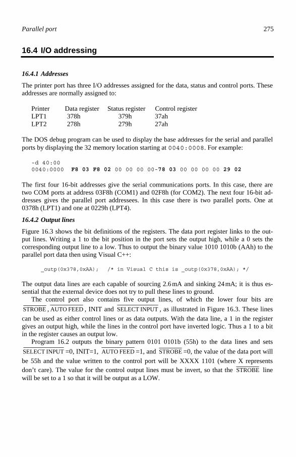
Parallel port 275
16.4 I/O addressing
16.4.1 Addresses
The printer port has three I/O addresses assigned for the data, status and control ports. These addresses are normally assigned to: Printer Data register Status register Control register LPT1 378h 379h 37ah LPT2 278h 279h 27ah The DOS debug program can be used to display the base addresses for the serial and parallel ports by displaying the 32 memory location starting at 0040:0008. For example:
-d 40:00 0040:0000 F8 03 F8 02 00 00 00 00-78 03 00 00 00 00 29 02
The first four 16-bit addresses give the serial communications ports. In this case, there are two COM ports at address 03F8h (COM1) and 02F8h (for COM2). The next four 16-bit ad-dresses gives the parallel port addressees. In this case there is two parallel ports. One at 0378h (LPT1) and one at 0229h (LPT4).
16.4.2 Output lines
Figure 16.3 shows the bit definitions of the registers. The data port register links to the out-put lines. Writing a 1 to the bit position in the port sets the output high, while a 0 sets the corresponding output line to a low. Thus to output the binary value 1010 1010b (AAh) to the parallel port data then using Visual C++:
_outp(0x378,0xAA); /* in Visual C this is _outp(0x378,0xAA); */ The output data lines are each capable of sourcing 2.6 mA and sinking 24 mA; it is thus es-sential that the external device does not try to pull these lines to ground. The control port also contains five output lines, of which the lower four bits are STROBE , FEED AUTO , INIT and INPUT SELECT , as illustrated in Figure 16.3. These lines can be used as either control lines or as data outputs. With the data line, a 1 in the register gives an output high, while the lines in the control port have inverted logic. Thus a 1 to a bit in the register causes an output low. Program 16.2 outputs the binary pattern 0101 0101b (55h) to the data lines and sets
INPUT SELECT =0, INIT=1, FEED AUTO =1, and STROBE =0, the value of the data port will be 55h and the value written to the control port will be XXXX 1101 (where X represents don’t care). The value for the control output lines must be invert, so that the STROBE line will be set to a 1 so that it will be output as a LOW.

276 Computer busses
D7
D6
D5
D4
D3
D2
D1
D0
Busy
ACK
PE
SELECT
ERROR
IRQ
Reserved
Reserved
Reserved
Reserved
Direction
IRQ ENABLE
SELECT INPUT
INIT
AUTOFEED
STROBE
Dataport
Statusport
Controlport
Figure 16.3 Port assignments
Program 16.2
#define DATA 0x378 #define STATUS DATA+1 #define CONTROL DATA+2 int main(void) int out1,out2; out1 = 0x55; /* 0101 0101 */ _outp(DATA, out1); out2 = 0x0D; /* 0000 1101 */ _outp(CONTROL, out2); /* STROBE=LOW, AUTOFEED=HIGH, etc */ return(0);
The setting of the output value (in this case, out2) looks slightly confusing as the output is the inverse of the logical setting (that is, a 1 sets the output low). An alternative method is to exclusive-OR (EX-OR) the output value with $B which will invert the 1st, 2nd and 4th least significant bits ( INPUT SELECT =0, FEED AUTO =1, and STROBE =0), while leaving the 3rd least significant bit (INIT) untouched. Thus the following will achieve the same as the previ-ous program: out2 = 0x06; /* 0000 0110 */ _outp(CONTROL, out2 ^ 0xb); /* STROBE=LOW, AUTOFEED=HIGH, etc */
If the 5th bit on the control register (IRQ enable) is written as 1 then the output on this line will go from a high to a low which will cause the processor to be interrupted. The control lines are driven by open collector drivers pulled to +5 Vdc through 4.7 kΩ resistors. Each can sink approximately 7 mA and maintain 0.8 V down-level.

Parallel port 277
SELECT INPUT
INIT
AUTOFEED
STROBE1
14
16
17
Control register
Data register
D02
D79
Figure 16.4 Output lines
16.4.3 Inputs
There are five inputs from the parallel port (BUSY, ACK , PE, SELECT and ERROR ). The status of these lines can be found by simply reading the upper 5 bits of the status register, as illustrated in Figure 16.5.
BUSY
ACK
PE
SELECT
ERROR15
13
12
10
11
Status register
Figure 16.5 Input lines
Unfortunately, the BUSY line has an inverted status. Thus when a LOW is present on BUSY, the bit will actually be read as a 1. For example Program 16.3 reads the bits from the

278 Computer busses
status register, inverts the BUSY bit and then shifts the bits three places to the right so that the five inputs bit are in the five least significant bits. Program 16.3
#include <stdio.h> #define DATA 0x378 #define STATUS DATA+1 int main(void) unsigned int in1; in1 = _inp(STATUS); /* read from status register */ in1 = in1 ^ 0x80 /* invert BUSY bit */ in1 = in1 >> 3; /* move bits so that the inputs are the least significant bits */ printf(″Status bits are %d\n″,in1); return(0);
16.4.4 Electrical interfacing
The output lines can be used to drive LEDs. Figure 16.6 shows an example circuit where a LOW output will cause the LED to be ON while a HIGH causes the output to be OFF. For an input an open push button causes a HIGH on the input.
5 V
5 V
GND
D0-D7
Controllines
330 Ω
10 KΩ
Figure 16.6 Interfacing to inputs and outputs
16.4.5 Simple example
Program 16.4 uses a push button connected to pin 11 (BUSY). When the button is open then the input to BUSY will be a HIGH and the most significant bit in the status register will thus be a 0 (as the BUSY signal is inverted). When the button is closed then this bit will be a 1.

Parallel port 279
This is tested with
if (in1&0x80)==1) When this condition is TRUE (that is, when the button is closed) then the output data lines (D0–D7) will flash on and off with a delay of 1 second between flashes. An output of all 1s to the data lines causes the LEDs to be off, and all 0s cause the LEDs to be on.
Program 16.4 /* Flash LEDs on and off when the push button connected to BUSY */ /* is closed */ #include <stdio.h> #include <dos.h> #define DATA 0x378 #define STATUS DATA+1 #define CONTROL DATA+2 int main(void) int in1; do in1 = _inp(STATUS); if (in1&0x80)==1) /* if switch closed this is TRUE */ _outp(DATA,0x00); /* LEDs on */ delay(1000); _outp(DATA, 0xff); /* LEDs off */ delay(1000); else _outp(DATA,0x01); /* switch open */ while (!kbhit()); return(0);
16.5 Interrupt-driven parallel port
16.5.1 Introduction
The previous section discusses how the parallel port is used to output data. This chapter dis-cusses how an external device can interrupt the processor. It does this by hooking onto the interrupt server routine for the interrupt that the port is attached to. Normally this interrupt routine serves as a printer interrupt (such as lack of paper, paper jam and so on). Thus, an external device can use the interrupt service routine to transmit data to or from the PC.
16.5.2 Interrupts
Each parallel port is hooked to an interrupt. Normally the primary parallel port is connected to IRQ7. It is assumed in this section that this is the case. As with the serial port this interrupt line must be enabled by setting the appropriate bit in the interrupt mask register (IMR),

280 Computer busses
which is based at address 21h. The bit for IRQ7 is the most significant bit, and it must be set to a 0 to enable the interrupt. As with the serial port, the end of interrupt signal must be acknowledged by setting the EOI signal bit of the interrupt control register (ICR) to a 1. See Section 8.5.2 for more information on these operations. The interrupt on the parallel port is caused by the ACK line (pin 10) going from a high to a low (just as a printer would acknowledge the reception of a character). For this interrupt to be passed to the PIC then bit 4 of the control port (IRQ Enable) must be set to a 1.
16.5.3 Example program
Program 16.5 is a simple interrupt-driven parallel port Borland C program. The program in-terrupts the program each time the ACK line is pulled LOW. When this happens the output value should change corresponding to a binary count (0000 0000 to 1111 1111, and then back again). The user can stop the program by pressing any key on the keyboard. Figure 16.7 shows a sample set-up with a push button connected to the ACK line and LEDs connected to the output data lines.
D0
ACK
5 V
330 Ω
5 V
GND
10 KΩ
10
5 V
330 Ω
D7
2
9
Figure 16.7 Example set-up for interrupt-driven parallel port
Program 16.5
/* Program to sample data from the parallel port */ /* when the ACK line goes low */ #include <stdio.h> #include <bios.h> #include <conio.h> #include <dos.h> #define TRUE 1 #define FALSE 0 #define DATA 0x378 #define STATUS DATA+1 #define CONTROL DATA+2 #define IRQ7 0x7F /* LPT1 interrupt */

Parallel port 281
#define EOI 0x20 /* End of Interrupt */ #define ICR 0x20 /* Interrupt Control Register */ #define IMR 0x21 /* Interrupt Mask Register */ void interrupt far pl_interrupt(void); void setup_parallel (void); void set_vectors(void); void enable_interrupts(void); void disable_interrupts(void); void reset_vectors(void); void interrupt far (*oldvect)(); int int_flag = TRUE; int outval=0; int main(void) set_vectors(); setup_parallel(); do if (int_flag) printf("New value sent\n"); int_flag=FALSE; while (!kbhit()); reset_vectors(); return(0); void setup_parallel(void) outportb(CONTROL, inportb(CONTROL) | 0x10); /* Set Bit 4 on control port to a 1 */ void interrupt far pl_interrupt(void) disable(); outportb(DATA,outval); if (outval!=255) outval++; else outval=0; int_flag=TRUE; outportb(ICR,EOI); enable(); void set_vectors(void) int int_mask; disable(); /* disable all ints */ oldvect=getvect(0x0f); /* save any old vector */ setvect (0x0f,pl_interrupt); /* set up for new int serv */ void enable_interrupts(void) int ch; disable(); ch=inportb(IMR); outportb(IMR, ch & IRQ7); enable();

282 Computer busses
void disable_interrupts(void) int ch; disable(); outportb(IMR, ch & ~IRQ7); enable(); void reset_vectors(void) setvect(0x0f,oldvect);
16.5.4 Program explanation
The initial part of the program enables the interrupt on the parallel port by setting bit 4 of the control register to 1: void setup_parallel(void) outportb(CONTROL, inportb(CONTROL) | 0x10); /* Set Bit 4 on control port*/
After the serial port has been initialized the interrupt service routine for the IRQ7 line is set to point to a new ‘user-defined’ service routine. The primary parallel port LPT1: normally sets the IRQ7 line active when the ACK line goes from a high to a low. The interrupt associated with IRQ7 is 0Fh (15). The getvect() function gets the ISR address for this interrupt, which is then stored in the variable oldvect so that at the end of the program it can be restored. Finally, in the set_vectors() function, the interrupt assigns a new ‘user-defined’ ISR (in this case it is the function pl_interrupt()): void set_vectors(void) int int_mask; disable(); /* disable all ints */ oldvect=getvect(0x0f); /* save any old vector */ setvect (0x0f,pl_interrupt); /* set up for new int serv */
At the end of the program the ISR is restored with the following code: void reset_vectors(void) setvect(0x0f,oldvect);
To enable the IRQ7 line on the PIC, bit 5 of the IMR (interrupt mask register) is to be set to a 0 (zero). The statement ch = inportb(IMR) & 0x7F;
achieves this as it bitwise ANDs all the bits, except for bit 7, with a 1. This is because any bit

Parallel port 283
which is ANDed with a 0 results in a 0. The bit mask 0x7F has been defined with the macro IRQ7: void enable_interrupts(void) int ch; disable(); ch=inportb(IMR); outportb(IMR, ch & IRQ7); enable();
At the end of the program the interrupt on the parallel port is disabled by setting bit 7 of the IMR to a 1; this disables IRQ7 interrupts: void disable_interrupts(void) int ch; disable(); outportb(IMR, ch & ~IRQ7); enable();
The ISR for the IRQ7 function is set to pl_interrupt(). It outputs the value of outval, which is incremented each time the interrupt is called (note that there is a roll-over statement which resets the value of outval back to zero when its value is 255). At the end of the ISR the end of interrupt flag is set in the interrupt control register with the statement out-portb(ICR, EOI);,as follows: void interrupt far pl_interrupt(void) disable(); outportb(DATA,outval); if (outval!=255) outval++; else outval=0; int_flag=TRUE; outportb(ICR,EOI); enable();
The main() function calls the initialisation and the de-initialisation functions. It also contains a loop which continues until any key is pressed. Within this loop, the keyboard is tested to determine if a key has been pressed. The interrupt service routine sets int_flag. If the main routine detects that it is set it displays the message ‘New value sent’ and resets the flag: int main(void) set_vectors(); outportb(CONTROL, inportb(CONTROL) | 0x10); /* set bit 4 on control port to logic one */ do if (int_flag) printf("New value sent\n"); int_flag=FALSE; while (!kbhit());

284 Computer busses
reset_vectors(); return(0);
16.6 Exercises
16.6.1 How many pins does a standard D-type parallel port connector have: (a) 9 (b) 12 (c) 25 (d) 36 16.6.2 How many data bits can the parallel port transmit at a time: (a) 8 (b) 12 (c) 16 (d) 32 16.6.3 What is the major limitation of a standard Centronics parallel port: (a) It is only an output (b) It is not compatible with many printers (c) Incompatibility of software (d) Limited cable types 16.6.4 What is the maximum data of a standard Centronics parallel port: (a) 15 kbps (b) 150 kbps (c) 1.5 Mbps (d) 10 Mbps 16.6.5 What is the standard I/O base address for a standard parallel port: (a) 3F8h (b) 378h (c) 2F8h (d) 278h 16.6.6 What is the standard I/O base address for a secondary parallel port: (a) 3F8h (b) 378h (c) 2F8h (d) 278h 16.6.7 What is the standard interrupt line for a standard parallel port: (a) IRQ3 (b) IRQ4 (c) IRQ5 (d) IRQ7 16.6.8 Write a program that sends a ‘walking-ones’ code to the parallel port. The delay
between changes should be 1 second. A ‘walking-ones’ code is as follows:

Parallel port 285
00000001 00000010 00000100 00001000 : : 10000000 00000001 00000010 and so on. Hint: Use a do…while loop with either the shift left operators (<<) or output the
values 0x01, 0x02, 0x04, 0x08, 0x10, 0x20, 0x40, 0x80, 0x01, 0x02, and so on. 16.6.9 Write separate programs which output the patterns in (a) and (b). The sequences
are as follows: (a) 00000001 (b) 10000001 00000010 01000010 00000100 00100100 00001000 00011000 00010000 00100100 00100000 01000010 01000000 10000001 10000000 01000010 01000000 00100100 00100000 00011000 00010000 00100100
: : and so on. 00000001 00000010 and so on. 16.6.10 Write separate programs which output the following sequences: (a) 1010 1010 (b) 1111 1111 0101 0101 0000 0000 1010 1010 1111 1111 0101 0101 0000 0000 and so on. and so on. (c) 0000 0001 (d) 0000 0001 0000 0011 0000 0011 0000 1111 0000 0111 0001 1111 0000 1111 0011 1111 0001 1111 0111 1111 0011 1111 1111 1111 0111 1111 0000 0001 1111 1111 0000 0011 0111 1111 0000 0111 0011 1111 0000 1111 0001 1111 0001 1111 0000 1111
and so on. and so on. (e) The inverse of (d) above.

286 Computer busses
16.6.11 Binary coded decimal (BCD) is used mainly in decimal displays and is equivalent to the decimal system where a 4-bit code represents each decimal number. The first 4 bits represent the units, the next 4 the tens, and so on. Write a program that outputs to the parallel port a BCD sequence with a 1-second delay between changes. A sample BCD table is given in Table 16.3. The output should count from 0 to 99.
Hint: One possible implementation is to use two variables to represent the units
and tens. These would then be used in a nested loop. The resultant output value will then be (tens << 4)+units. An outline of the loop code is given next.
for (tens=0;tens<10;tens++) for (units=0;units<10;units++)
Table 16.3 BCD conversion
Digit BCD 00 01 02 03 04 05 06 07 08 09 10 11
00000000 00000001 00000010 00000011 00000100 00000101 00000110 00000111 00001000 00001001 00010000 00010001
. . .
. . .
97 98 99
10010111 10011000 10011001
16.6.12 Write a program which interfaces to a 7-segment display and displays an incre-
mented value every second. Each of the segments should be driven from one of the data lines on the parallel port. For example:
Value Segment Hex A B C D E F G value 0 1 1 1 0 1 1 1 77h 1 0 0 1 0 0 1 0 12h 2 1 1 0 1 0 1 1 6Bh : : : 9 0 0 1 1 1 1 1 1Fh
Two ways of implementing this is either to determine the logic for each segment
or to have a basic look-up table, such as:
E
B
F
C
A
D
G

Parallel port 287
int seg_val[8]=0x77, 0x12, 0x6B, … 0x1F; val=seq_val(count % 10); /* mask-off the least-significant digit */ outportb(0x378,seg_val[val]);
16.6.13 Write a program counts the number of pushes of a button. The display should
show the value. 16.6.14 Modify the program developed in Exercise 16.6.13 so that it outputs the count
value to the parallel port. 16.6.15 Modify the program developed in Exercise 16.6.14 so that the display is incre-
mented when the user presses a button. 16.6.16 Write a program in which the user presses a button which causes the program to
read from the parallel port. 16.6.17 Write a printer driver in which a string buffer is passed to it and this is then out-
putted to the printer. The driver should include all the correct error checking (such as out-of-paper, and so on).
16.7 Notes from the author
The parallel port is hardly the greatest piece of technology. In its truly standard form, it only allows for simplex communications, from the PC outwards. However, like the RS-232 port, it’s a standard part of the PC, and its cheap. So, interface designers have worked under dif-ficult circumstances to try and improving its specification, such as increasing its bit rate and allowing multiple devices to connect to it at the same time, but it still suffers from a lack of controllability. Anyone who has changed the interface of a device from the parallel port to the USB will know how much better the USB port is over the parallel port. The parallel port and RS-232 are the two top requests that I get from users, especially related to project work. The Top 10 requests, in order of the most requests I have received, are: 1. RS-232. 2. Parallel Port. 3. Converting a DOS program to Microsoft Windows. 4. Borland Delphi interfacing. 5. ISA card design.
6. Interrupt-driven software. 7. PCMCIA. 8. Network card design. 9. Visual Basic interfacing 10. Using buffered systems.
One of the most amusing emails that I ever received related to an ISA card which I had drawn. In the card, I had drawn a few chips, to basically show that it had some electronics on it. So that the chips would not be confused with real chips I labelled one of them XYZ123. One user sent me an email saying: ‘Thanks for … Please could you tell me the function of the XYZ123 device. I have searched for this component, and cannot find any information on it. Please could you send me some’

288 Computer busses
I didn’t really have the heart to write back to the user and say that it was a made-up chip, so I sent an email back saying that it was not available at the present time (which was true). So why has the serial port become more popular than the parallel port. Well it’s because of one reason: since PC’s started, the serial port has always been a standard port and most manufacturers abide with it, whereas the parallel port was a quick fix so that the original PC could communicate with a printer. In its standard form, it can only send information in a single direction, and, even worse, only eight bits can be sent at a time. Nevertheless, it has survived, and now has several uses, especially with printers, scanners and external CD-ROMs. So it will hold the fort for a few years yet before the USB port takes over in creating a truly integrated bus system. But, you may say, the USB port is serial. So why transmit one bit at a time when you can transmit 8 or 16 or even 32 bits at a time. Well it’s all to do with the number of wires that must be connected. A serial bus always has the advantage over a paral-lel bus, in that you only really need one signal line in a serial bus to transmit all the data. This saves space in both the connector, and in the cable. It is also cheaper to install. Personally, I think that there is no better bus for a student to start to learn how to inter-face to external devices. It is relatively easy to build the interface electronics, and to connect a few LEDs. How great it is to see a student’s face after they have written their first program to make a few LEDs flash on and off. I remember a third year student commented: ‘I’ve been programming for three years, and finally, we’re doing something real.’ Whether you agree with this comment or not depends on the type of programming that you would like to do. Some of us like doing databases, some like writing user-interfaces, but there are lots who like to make computers sense things and make physical things happen. In the past, especially in the 1970s and 1980s, electronic engineers used breadboards and wires to prototypes cir-cuits. Sometimes the circuits blew-up, or times they would stop working, but at least you knew where you were with the electronics. These days with massively integrated circuits, it is difficult to know one end of a microchip from another. They normally work first time, they’re easy to connect to, and when they don’t work you just throw them in the bin. Image the size of the bin that would have been required if someone had had build a Pentium processor from the discrete transistors (over 20 million of them). Image the heat that would have been gen-erated. Assuming 15mW for each transistor, the total power would be 300kW, which is equivalent to the heat given of by 3000 100W light builds, or 300 1kW heaters. So it shows how far we have come in such a short time, as now we can touch the processor, and it just feels a little hot. Personally, I would have no problems in going back to the days when tran-sistors had three legs and a tin hat, and you had to look up a data sheet to tell which of the legs was the base, and which was the collector. So, as the technology has moved on, the parallel port seems like an old friend. It has watched the PC develop as the inners have become more integrated and faster, but it has never really been a high flier, preferring instead to quietly perform its duties without much bother. From CGA and EGA to VGA, from the serial port to the USB port, from 5.25inch floppy disks to 6550MB CD-ROMs, and so on. But, there’s no way that the parallel port could be allowed to stay as it was in the original parallel specification. It has potential, but that potential is severely limited because it must always keep compatibility with previous ports. So how is it possible to connect a printer on the parallel port, and other devices, with-out the printer reading communications that are destined for another device. If it wasn’t the PC, the designers would have simply ripped up the original specification, and started again. But, you don’t do that with the PC, or you’ll not sell. So, we’ll see in the next chapter how the parallel port has been dragged into the modern age. But, as we’ll see, it’s more like a difficult toddler, than an enterprising businessman. The prize for the best upgrade goes to Ethernet, which has increased its transmission rate by a factor of 100 (10Mbps to 1Gbps).

Enhanced Parallel Port
17.1 Introduction
The Centronics parallel port only allows data to be sent from the host to a peripheral. To overcome this the IEEE published the 1284 standard, entitled ‘Standard Signaling Method for a Bidirectional Parallel Peripheral Interface for Personal Computers’. It allows for bi-directional communication and high communication speeds, while being backwardly com-patible with existing parallel ports. The IEEE-1284 standard defines the following modes: • Compatibility mode (forward direction only) – This mode defines the transfer of data
between the PC and the printer (Centronics mode, as covered in the previous chapter). • Nibble mode (reverse direction) – This mode defines how four bits are transferred, at a
time, using status lines for the input data (sometimes known as Hewlett Packard Bi-tronics). The Nibble mode can thus be used for bidirectional communication, with the data lines being used as outputs. To input a byte, requires two nibble cycles.
• Byte mode (reverse direction) – This mode defines how eight bits are transferred at a time.
• Enhanced parallel port (EPP) – This mode defines a standard bidirectional communica-tions and is used by many peripherals, such as CD-ROMs, tape drives, external hard disks, and so on.
In the IEEE 1284 standard the control and status signal for nibble, byte and EPP modes have been renamed. It also classifies the modes as forward (data goes from the PC), reverse (data is input into the PC) and bidirectional. Both the compatibility and nibble modes can be im-plemented with all parallel ports (as the nibble mode uses the status lines and the compatibil-ity mode only outputs data). Some parallel ports support input and output on the data lines and thus support the byte mode. This is usually implemented by the addition of a direction bit on the control register.
17.2 Compatibility mode
The compatibility mode was discussed in Chapter 16. In this mode, the program sends data to the data lines and then sets the STROBE LOW and then HIGH. These then latch the data to the printer. The operations that the program does are: 1. Data is written to the data register.
17

290 Computer busses
2. The program reads from the status register to test to see if the BUSY signal is LOW (that is, the printer is not busy)
3. If the printer is not busy then the program sets the STROBE line active LOW. 4. Program then makes the STROBE line HIGH by de-asserting it.
STROBE
ACK
BUSY
DATAValid data
0.5ms (min.)5 ms (min.)
Figure 17.1 Compatibility mode transfer
17.3 Nibble mode
This mode defines how four bits are transferred, at a time, using status lines for the input data (sometimes known as Hewlett Packard Bi-tronics). The Nibble mode can thus be used for bi-directional communication, with the data lines being used as outputs. To input a byte, re-quires two nibble cycles. As seen in Chapter 16 there are five inputs from the parallel port (BUSY, ACK , PE, SELECT and ERROR ). The status of these lines can be found by simply reading the upper
five bits of the status register. The BUSY, PE, SELECT and ERROR are normally used as ACK used to interrupt the processor. Table 17.1 defines the names of the signal in the nibble mode and Figure 17.2 shows the handshaking for this mode. The nibble mode has the following sequence: 1. Host (PC) indicates that it is ready to receive data by setting HostBusy LOW. 2. The peripheral then places the first nibble on the status lines. 3. The peripheral indicates that the data is valid on the status line by setting PtrClk low. 4. The host then reads from the status lines and sets HostBusy high to indicate that it has
received the nibble, but it is not yet ready for another nibble. 5. The peripheral sets PtrClk HIGH as an acknowledgement to the host. 6. Repeat steps 1–5 for the second nibble.

Enhanced parallel port 291
Table 17.1 Nibble mode signals
Compatibility signal name
Nibble mode name In/out Description
STROBE STROBE Out Not used.
FEED AUTO HostBusy Out Host nibble mode handshake signal. It is set LOW to indicate that the host is ready for nib-ble and set HIGH when the nibble has been received.
INPUT SELECT 1284Active Out Set HIGH when the host is transferring data.
INIT INIT Out Not used.
ACK PtrClk In Indicates valid data on the status lines. It is set low to indicate that there is valid data on the control lines and then set HIGH when the Host-Busy going high.
BUSY PtrBusy In Data bit 3 for one cycle then data bit 7.
PE AckDataReq In Data bit 2 for one cycle then data bit 6.
SELECT Xflag In Data bit 1 for one cycle then data bit 5.
ERROR DataAvail In Data bit 0 for one cycle then data bit 4.
D0–D7 D0–D7 Not Used.
HostBusy
DATA lines(PtrBusy, AckDataReq, XFlag and DataAval)
Valid dataBits 0-3
Valid dataBits 4-7
PtrClk
Figure 17.2 Nibble mode data transfer cycle
These operations are software intensive as the driver requires to set and read the handshaking lines. This limits transfer to about 50 kBps. Its main advantage is that it will work with all printer ports because it uses the standard Centronics set-up and is normally used in low-speed bi-directional operations, such as ADC adapters, reading data from switches, and so on. Figure 17.3 illustrates the operation of the nibble mode, where four data bits are read into the parallel port using the four input handshaking lines. The status of these lines is then read by interrogating the upper four bits of the status register. This method is fine when there is

292 Computer busses
no handshaking and when there are four, or less, data bits to be read in. If there are more, or if there is handshaking, then extra circuitry is required.
PtrBusy (BUSY)
AckDataReq (PE)
XFlag (SELECT)
DataAvail (ERROR)
b7 b6 b5 b4 b3 b2 b1 b0
Status port (379h)
inval=(_inp(0x379) & 0xf0) >> 4
Datainput
Figure 17.3 Nibble mode interfacing
Figure 17.4 shows how the nibble mode can be used to read-in eight bits at a time. For this one bit of the data output lines (D0) is used to select either the upper four bits or the lower four bits of the 8-bit data byte. If D0 is a low (0) then the lower four bits are selected, else if it is a high (1) then the upper four bits are selected. The D0 output line connects to a multiplexor which will select the lower or the upper four bits. If A is the multiplexor selector line, X[1:4] are the input data bits and Z[1:4] the output from the multiplexor, then the equa-tion for the multiplexor is ]1[]5[]1[ XAAXZ += ]2[]6[]2[ XAAXZ += ]3[]7[]3[ XAAXZ += ]4[]8[]4[ XAAXZ +=
A
X[1]
X[5]Z[1]

Enhanced parallel port 293
PtrBusy (BUSY)
AckDataReq (PE)
XFlag (SELECT)
DataAvail (ERROR)
b7 b6 b5 b4 b3 b2 b1 b0
Status port (379h)
_outp(0x378,0); /* set lower 4 bits */inval1=(_inp(0x379) & 0xf0) >> 4;_outp(0x378,1); /* set upper 4 bits */inval=(_inp(0x379) & 0xf0) +inval1;
b7 b6 b5 b4 b3 b2 b1 b0
Multiplexor(1 of 2)
Data port (378h)
D0
0
1
8-bi
t dat
a in
put
Figure 17.4 Nibble mode for 8-bit input
17.4 Byte mode
The byte mode is often known as a bidirectional port and it uses bidirectional data lines. It has the advantage over nibble mode in that it only takes a single cycle to transfer a byte. Un-fortunately, it is only compatible with newer ports. Table 17.2 defines the names of the sig-nal in the nibble mode and Figure 17.5 shows the handshaking for this mode. The byte mode has the following sequence: 1. Host (PC) indicates that it is ready to receive data by setting HostBusy LOW. 2. The peripheral then places the byte on the status lines. 3. The peripheral indicates that the data is valid on the status line by setting PtrClk LOW. 4. The host then reads from the data lines and sets HostBusy HIGH to indicate that it has
received the nibble, but it is not yet ready for another nibble. 5. The peripheral sets PtrClk HIGH as an acknowledgement to the host. 6. Host then acknowledges the transfer by pulsing HostClk.

294 Computer busses
Table 17.2 Byte-mode signals
Compatibility signal name
Byte-mode name In/Out Description
STROBE HostClk Out Used as an acknowledgment signal. It is pulsed low after each transferred byte.
FEED AUTO HostBusy Out It is set LOW to indicate that the host is ready for nibble and set HIGH when the nib-ble has been received.
INPUT SELECT 1284Active Out Set HIGH when the host is transferring data.
INIT INIT Out Not used.
ACK PtrClk In Indicates valid data byte. It is set LOW to indicate that there is valid data on the data lines and then set HIGH when the HostBusy going high.
BUSY PtrBusy In Busy status (for forward direction).
PE AckDataReq In Same as DataAvail .
SELECT Xflag In Not used.
ERROR DataAvail In Indicates that there is reverse data available.
D0–D7 D0–D7 In/Out Input/output data lines.
HostBusy
Valid data
PtrClk
Data
HostClk
Figure 17.5 Byte mode data transfer cycle
17.5 EPP
The enhanced parallel port (EPP) mode defines a standard bidirectional communications mode and is used by many peripherals, such as CD-ROMs, tape drives, external hard disks and so on. The EPP protocol provides four types of data transfer cycles:

Enhanced parallel port 295
1. Data read and write cycles – These involve transfers between the host and the peripheral. 2. Address read and write cycles – These pass address, channel, or command and control
information. Table 17.3 defines the names of the signal in the nibble mode. The WRITE occurs automati-cally when the host writes data to the output lines. The data write cycle has the following sequence: 1. Program executes an I/O write cycle to the base address port + 4 (EPP data port), see Ta-
ble 17.4. Then the following occur with hardware: 2. The WRITE line is set LOW, which puts the data on the data bus. 3. The DATASTB is then set LOW. 4. The host waits for peripheral to set the WAIT line HIGH. 5. The DATASTB and WRITE are then HIGH and the cycle ends. The important parameter is that it takes just one memory-mapped I/O operation to transfer data. This gives transfer rates of up to 2 million bytes per second. Although it is not as fast as a peripheral transferring over the ISA, it has the advantage that the peripheral can transfer data at a rate that is determined by the peripheral.
Table 17.3 EPP mode signals
Compatibility signal name
EPP mode name
In/out Description
STROBE WRITE Out A LOW for a write operation while a HIGH indi-cates a read operation.
FEED AUTO DATASTB Out Indicates a data read or write operation.
INPUT SELECT ADDRSTROBE
Out Indicates an address read or write operation.
INIT
RESET Out Peripheral reset when LOW.
ACK INTR In Peripheral sets this line LOW when it wishes to interrupt to the host.
BUSY WAIT In When it is set LOW it indicates that it is valid to start a cycle, else if it is HIGH then it is valid to end the cycle.
PE User defined In Can be set by each peripheral.
SELECT User defined In Can be set by each peripheral.
ERROR User defined In Can be set by each peripheral.
D0–D7 AD0–AD7 In/out Bidirectional address and data lines.

296 Computer busses
17.5.1 EPP registers
Several extra ports are defined, these are the EPP address register and EPP data register. The EPP address register has an offset of three bytes from the base address and the EPP data reg-ister is offset by four bytes. Table 17.4 defines the registers.
Table 17.4 EPP register definitions
Port Name I/O address Read/ write
Description
Data register BASE_AD W
Status register
BASE_AD +1 R
Control register
BASE_AD +2 W
EPP address port BASE_AD+3 R/W Generates EPP address read or write cycle
EPP data port BASE_AD+4 R/W Generates EPP data read or write cycle
17.6 ECP
The extended capability port (ECP) protocol was proposed by Hewlett Packard and Micro-soft as an advanced mode for communication with printer and scanner type peripherals. It provides a high performance bidirectional data transfer between a host and a peripheral. The standard provides for two cycle types in both forward and reverse directions: 1. Data cycles. 2. Command cycles which can either be a run length count or a channel address. It has many advantages over the EPP standard, including: • Standard addresses – ECP has standard register addresses – Figure 17.6 shows that the
addresses from 0778h to 077Ah have been defined for the extra functionality of ECP. • Run length encoding (RLE) – RLE allows for compression. It allows high compression
rates when there is a great deal of repetitive information in a file (typically with graphics files). A repetitive sequence is identified by a count followed by the repeated byte.
• FIFOs for both the forward and reverse channels. • DMA as well as programmed I/O for the host register interface. • Channel addressing – This allows multiple logical devices to be located within a single
physical device. This channel address is passed in the command phase and can support up to 128 devices (addresses 0 to 127). For example, a single unit could have an integrated printer, fax and modem. ECP channel address allows them all to be accessed over a sin-gle connection. Within one physical package, having a single parallel port attached, there is a printer, fax and modem. This has the advantage that the printer can be busy printing while the modem can be accessed at the same time.
ECP redefines the SPP signals to be consistent with the ECP handshake. Table 17.5 de-

Enhanced parallel port 297
scribes these signals. Figure 17.7 shows two forward data transfer cycles. It has data followed by a command phase. A high on the HostAck line indicates a data cycle, whereas a low indicates a com-mand cycle. In the low state (command cycle) the data either represents an RLE count or a channel address. The most significant bit of the data byte indicates whether it is an RLE count or a channel address. If it is a 0, then bits the other 7 bits represent a RLE Count (from 0 to 127), else a 1 represents a channel address (from 0 to 127).
Figure 17.6 ECP input/output address ranges
Table 17.5 ECP mode signals
Compatibility signal name
ECP mode name In/out Description
STROBE
HostClk I Transfers data or address information in the forward direction (along with Pe-riphAck).
FEED AUTO HostAck O Command/Data status in the forward direction. Data transfer in reverse direc-tion (along with PeriphClk).
INPUT SELECT 1284Active O Set high when host is in a 1284 transfer mode.
INIT uestReverseReq O A low puts channnel in reverse direc-tion.
ACK PeriphClk I Transfer data in the reverse direction (along with HostAck).
BUSY PeriphAck I Transfer data or command information (along with HostClk).
PE nAckReverse I Acknowledgement to nReverseRequest.
SELECT Xflag I Extensibility flag.
ERROR nPeriphRequest I Set low by peripheral to indicate that reverse data is available.
D0–D7 Data[8:1] I/O Data lines.

298 Computer busses
HostClk
PeriphAck
D0-D7
HostAck Data Command
First byte Second byte
1 2 3 4
Figure 17.7 ECP forward data and command cycle
In the forward mode, the transfer of the data is from the host to the peripheral. Initially the host places its data on the data bus. It sets the HostAck line high to indicate a data cycle and sets HostClk low to indicate valid data. Next, the peripheral acknowledges the host by setting PeriphAck high. The host sets HostClk high which clocks the data into the peripheral. After this, the peripheral sets PeriphAck low to indicate that it is ready for the next byte. Figure 17.7 illustrates an example of the reverse channel transfer where the peripheral transfers information to the host. As before, it shows a command cycle followed by a data cycle. It is similar to the forward phase except that the host requests a reverse channel by setting the nReverseRequest low. The peripheral then sets the nAckReverse line low to indi-cate that it is ready to transfer data, then it puts the data on the data bus. It then sets the Pe-riphAck high to indicate that it is a data cycle and set PeriphClk low to indicate valid data. After this the host sets HostAck high to acknowledge these events and the peripheral sets PeriphClk high. This clock edge then clocks the data into the host. Finally, the host sets HostAck low to indicate that it is ready for the next byte.
17.6.1 ECP software and register interface
The ECP specification (‘The IEEE 1284 Extended Capabilities Port Protocol and ISA Inter-face Standard’) defines a number of operational modes. These are defined in Table 17.6. The registers used to program ECP are based on the standard parallel port setting and uses an address which are offset by 1024 (400h) from the standard port address. Thus: Standard port base address = 378h ECP extended registers = 378h + 400h = 778h There are six extra registers defined for ECP, these are given in Table 17.7. These six regis-ters are mapped into three memory addresses and are shown in Figure 17.8 (778h, 779h and 77Ah). The ECR register used to set the current operational mode and can also be used to determine if an ECP-capable port is installed in the PC. Detection software can try to access any ECR registers by adding 402h to the base address of the LPT ports identified in the BIOS LPT port table.

Enhanced parallel port 299
HostClk
PeriphAck
D0-D7
HostAck Data Command
First byte Second byte
nReverseRequest
nAckReverse
Figure 17.8 ECP Reverse data and command cycle
The operation of the ECP port is similar to the EPP port. The ECR register is used to set an operational mode, after which an I/O port is used to transfer data (the actual port depends on the mode). Handshaking is done automatically by the hardware and there is no need for the software to control it.
Table 17.6 ECR Register Modes
Mode Description Mode Description 000 SPP mode 100 EPP parallel port mode (note 1)
001 Bidirectional mode (byte mode)
101 (reserved)
010 Fast Centronics 110 Test mode
011 ECP parallel port mode 111 Configuration mode
Table 17.7 ECP register description
Offset Name Read/Write ECP Mode Function 000 Data R/W 000-001 Data register 000 ecpAfifo R/W 011 ECP address FIFO 001 dsr R/W all Status register 002 dcr R/W all Control register 400 cFifo R/W 010 Parallel port data FIFO 400 ecpDfifo R/W 011 ECP data FIFO 400 tfifo R/W 110 Test FIFO 400 cnfgA R 111 Configuration register A 401 cnfgB R/W 111 Configuration register B 402 ecr R/W all Extended control register

300 Computer busses
17.7 Exercises
17.8.1 How many pins does a standard D-type parallel port connector have: (a) 9 (b) 12 (c) 25 (d) 36 17.8.2 What is the maximum transfer rate for ECP/EPP mode: (a) 100 kB/s (b) 150 kB/s (c) 1 MB/s (d) 1.2 MB/s 17.8.3 Outline the operation of the nibble mode. How does the parallel port allow data to
be inputted? 17.8.4 Design a circuit for nibble mode operation which will sample data bits. The design
should include ground connections (GND), connector types and pin numbers. If possible, implement the design by adding switches to simulate input levels (power can be supplied by the parallel port connection).
17.8.5 Explain how several devices can be connected to the parallel port, and identify
how the operating system identifies each of the devices.
17.8 Note from the author
The parallel port was never really been destined for glory. It is basically a legacy port, which, in the past, was only really useful in connecting printers. The future for printer con-nections is either with network connections, such as Ethernet, or with a USB connection. In its standard form, it has a large, bulky connector, which in many systems is never even used. It has always struggled against the serial port, because it lacks the flexibility of RS-232 and, until recently, had no standards agency to support it. However, it’s there and it has great potential for fast data transfers. RS-232 has always been a great success and has many of the large manufacturers supporting it, and all importantly, it is defined by several stan-dards agencies. The key to its current success was due to the intervention of the NPA which brought together many of the leading computer and printer manufacturers. In these days, there are only a few major companies, such as Intel and Microsoft, who can lead the market and define new standards (such as the PCI bus, with Intel). The main difficulties are how to keep compatibility with previous implementations and software, and also how to connect multiple devices on a bus system, and allow them to pass data back and forward without interfering with other devices. This has finally been achieved with ECP/EPP mode. It is a bit complex, but it works, and even supports data compression. At the present, my notebook connects to a CD-R drive, a scanner and a printer, all of the same parallel port (just like SCSI). This arrangement works well most of the time and is a relative cheap way of connecting devices, but it is in no way as flexible and as fast a SCSI.
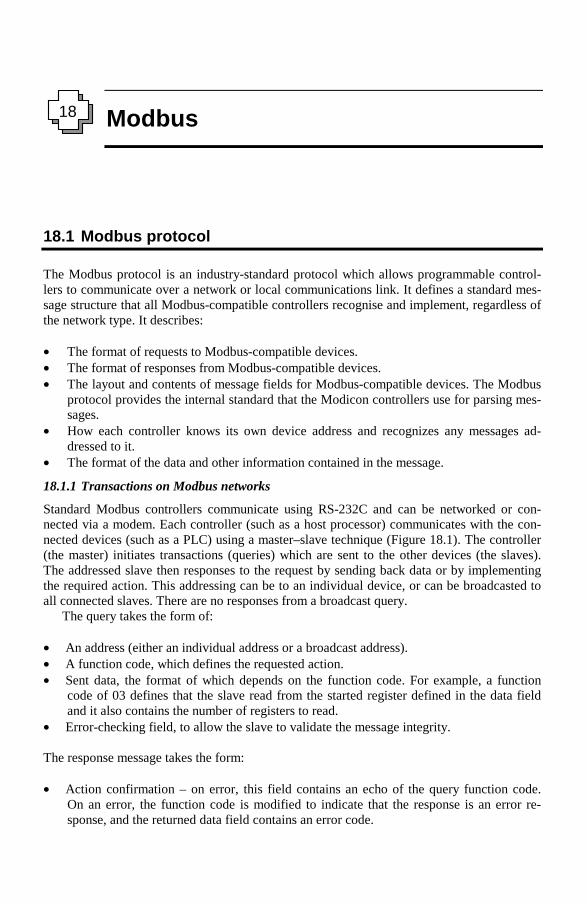
Modbus
18.1 Modbus protocol
The Modbus protocol is an industry-standard protocol which allows programmable control-lers to communicate over a network or local communications link. It defines a standard mes-sage structure that all Modbus-compatible controllers recognise and implement, regardless of the network type. It describes: • The format of requests to Modbus-compatible devices. • The format of responses from Modbus-compatible devices. • The layout and contents of message fields for Modbus-compatible devices. The Modbus
protocol provides the internal standard that the Modicon controllers use for parsing mes-sages.
• How each controller knows its own device address and recognizes any messages ad-dressed to it.
• The format of the data and other information contained in the message.
18.1.1 Transactions on Modbus networks
Standard Modbus controllers communicate using RS-232C and can be networked or con-nected via a modem. Each controller (such as a host processor) communicates with the con-nected devices (such as a PLC) using a master–slave technique (Figure 18.1). The controller (the master) initiates transactions (queries) which are sent to the other devices (the slaves). The addressed slave then responses to the request by sending back data or by implementing the required action. This addressing can be to an individual device, or can be broadcasted to all connected slaves. There are no responses from a broadcast query. The query takes the form of: • An address (either an individual address or a broadcast address). • A function code, which defines the requested action. • Sent data, the format of which depends on the function code. For example, a function
code of 03 defines that the slave read from the started register defined in the data field and it also contains the number of registers to read.
• Error-checking field, to allow the slave to validate the message integrity. The response message takes the form: • Action confirmation – on error, this field contains an echo of the query function code.
On an error, the function code is modified to indicate that the response is an error re-sponse, and the returned data field contains an error code.
18
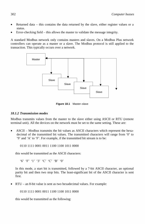
302 Computer busses
• Returned data – this contains the data returned by the slave, either register values or a status.
• Error-checking field – this allows the master to validate the message integrity. A standard Modbus network only contains masters and slaves. On a Modbus Plus network controllers can operate as a master or a slave. The Modbus protocol is still applied to the transaction. This typically occurs over a network.
Master
Slave
Slave
Slave
Slave
Figure 18.1 Master–slave
18.1.2 Transmission modes
Modbus transmits values from the master to the slave either using ASCII or RTU (remote terminal unit). All the devices on the network must be set to the same setting. These are: • ASCII – Modbus transmits the bit values as ASCII characters which represent the hexa-
decimal of the transmitted bit values. The transmitted characters will range from ‘0’ to ‘9’ and ‘A’ to ‘F’. For example, if the transmitted bit stream is to be:
0110 1111 0001 0011 1100 1100 1011 0000
this would be transmitted as the ASCII characters:
‘6’ ‘F’ ‘1’ ‘3’ ‘C’ ‘C’ ‘B’ ‘0’
In this mode, a start bit is transmitted, followed by a 7-bit ASCII character, an optional parity bit and then two stop bits. The least-significant bit of the ASCII character is sent first.
• RTU – an 8-bit value is sent as two hexadecimal values. For example:
0110 1111 0001 0011 1100 1100 1011 0000 this would be transmitted as the following:

Modbus 303
‘0110 1111’ ‘0001 0011’ ‘1100 1100’ ‘1011 0000’ which allows for a faster transmission of values, and they can thus be decoded quicker than the ASCII mode. RTU will obviously be twice as fast as the ASCII method. It also allows continuous bit streams to be transmitted. In this mode, a start bit is transmitted, followed by an 8-bit binary value, an optional parity bit and then two stop bits.
In summary, the modes are:
ASCII RTU Coding Hexadecimal characters 8-bit binary Start bits 1 1 No of bits/character 7 8 Parity Optional Optional Stop bits 1 or 2 1 or 2 Error checking LRC CRC
18.1.3 Modbus message frame
The Modbus message has different formats, depending on the transmission mode. These are: • ASCII framing – a colon ASCII character (:, or 3Ah) starts the message and the carriage
return–line feed sequence ends the message (CRLF, or 0Dh and 0Ah). The characters within the message will then be ‘0’ to ‘9’ or ‘A’ to ‘F’. On a network, devices continu-ally listen for the colon character. The field after this is the address field. The maximum interval between characters is one second. Figure 18.2 shows the standard format.
• RTU framing – messages start with a silent interval of at least 3.5 character times. After this, the device address is transmitted. All devices on the network listen to the bus, and wait for a silent period, which must be at least 3.5 characters since the last message. It then transmits the message as a continuous stream. The first eight bits are the target ad-dress. Errors occur if there is a silent period of more than 1.5 character times or if a de-vice transmits its message before 3.5 character delays after the previous message. Figure 18.2 shows the standard format.
Start(:) Address Function DATA LRC Check End
(CR-LF)
1 2 2 n 2 2Number ofcharacters:
Start Address Function DATA LRC Check End
3.5 characters 8 bits 8 bits n x 8 bits 16 bits 3.5 charactersTime:
ASCIIframe
RTUframe
Figure 18.2 ASCII and RTU message frame

304 Computer busses
18.1.4 Address field
The address field contains either two ASCII characters (for ASCII mode) or eight bits (for RTU mode). Addresses range from 0 to 247 (00h to F7h), where 0 is the broadcast address and 1 to 247 are used for slaves addresses. A master communicating with the slave puts the slave’s address in the address field, and the slave, when responding, puts its own address in the address field (to identify itself).
18.1.5 Function field
The function field contains either two ASCII characters (for ASCII mode) or eight bits (for RTU mode). Codes range from 1 to 255 (00h to FFh), and they are used by the master to inform the slave as to the action which requires to be performed. Typical codes (in decimal) are: 01 Read coil status 02 Read input status 03 Read holding registers 04 Read input registers 05 Force single coil 06 Preset single register 07 Read exception status 08 Diagnostics 11 Fetch comm. event counter 12 Fetch comm. event log 13 Program controller 14 Poll controller 15 Force multiple coils 16 Preset multiple registers 17 Report Slave ID 18 Program 884/M84 19 Reset communication link 20 Read general reference 21 Write general reference 22 Mask write 4x reference 23 Read/write 3x registers 24 Read FIFO queue For example, the read coil status gives an ON/OFF status for discrete outputs. When there are no errors the slave sends back the original function code, else, on an error, the same code is sent back, expect the most-significant bit is set to a 1. For example, if the function code was 0000 1000, then, on an error, the return value will be 1000 1000. A status code is also added in the data field, these are outlined in Table 18.1.
Table 18.1 Exception codes
Code Name Description 01 Illegal function The message function received is not an allowable action for the
addressed salve.
02 Illegal data address The address referenced in the data field is not an allowable address for the addressed slave location.
03 Illegal data value The value referenced in the data field is not allowable in the ad-dressed slave location.
04 Failure in associated device
The slave’s subcontroller has failed to respond to a message or an abortive error occurred.
05 Acknowledge The slave has accepted and is processing the long duration program command.
06 Busy, rejected mes-sage
The message was received without error, but the slave is currently busy.
For example, if the master sends the message

Modbus 305
Address Function Start address (hi) Start address (lo) No. (hi) No. (low) LRC :12 01 02 10 00 01 DA
Then on an error, the response would send back the function code of 81 (which sets the most significant bit of the function code (that is, 1000 0001). If the slave were busy then the ex-ception code would be 06. Thus the code sent back will be: Address Function Exception code LRC 12 81 06 67
18.1.6 Data field
The data fields contains even multiples of hexadecimal digits (in ASCII mode) or an even number of binary values (in RTU mode). The format of the field depends on the function code, and contains information, such as register addresses, the number of values required and the number of bytes in the data field. For example if the function code is 01 (read code status), then the format of the frame send from the master to the slave is: • Slave address (xx). • Function (01) – read coil status. • Starting address high (xx) – most-significant byte of the starting register address. • Starting address low (xx) – least-significant byte of the starting register address. • Number of Points high (xx) – most-significant byte of the number of points to be sent. • Number of Points low (xx) – least-significant byte of the number of points to be sent. • Error check (xx). If there are no errors, then the response is: • Slave address (xx). • Function (01) – read coil status. • Byte count. • Data (Coils 8 to 1) – data for the first eight coils, where a 1 value in a coil bit position
represents ON, whereas a 0 represent OFF. • Data (Coil 16 to 9) –data for the next eight coils. • etc. • Error check (xx). Some data fields are empty, such as the communication event log function (12, or 0Bh).
18.1.7 Error checking field
The error checking method depends on the type of transmission, these are: • ASCII – in this mode the error checking field contains two characters, which performs a
longitudinal redundancy check (LRC) for all characters, excluding the start and end ter-minating characters (:, CR and LF).
• RTU – in this mode, the error-checking field contains a 16-bit value which performs a cyclical redundancy check (CRC). This field is added to the end of the message; the low-order byte of the field is appended first, followed by the high-order byte.

306 Computer busses
LRC
The ASCII mode uses the LRC method. It basically adds up the values of each of the 8-bit fields, apart from the starting colon and the end CRLF, and then takes the two’s complement of the result (ignoring any carries). For example, from the previous example the transmitted values are
Start address (12) 0001 0010 Function (01) 0000 0001 Start address, high (02) 0000 0010 Start address, low (10) 0001 0000 Number, high (00) 0000 0000 Number, low (01) 0000 0001 Total 0010 0110
To convert to 2’s complement, invert all the bits, to give
1101 1001 and then add 1, to give
1101 1010 which is DA, in hexadecimal. Thus the transmitted message would be:
:120102100001DA<CRLF>
CRC checking
The RTU mode uses CRC, which is a much stronger error checking method. This method is outlined in Appendix D. Its operation is as follows: 1. 16-bit register is preloaded with all bits set to 1. 2. The first eight-bit data character is exclusive ORed (XOR) with the higher order-byte in
the register and the result is put in the register. 3. The register is then right shifted by one bit position and a zero filled into the most signifi-
cant bit (MSB) position. 4. If the shifted bit out is a 1, XOR the generator polynomial 1010 0000 0000 0001 with the
16-bit register, else return to Step 3. 5. Repeat steps 3 and 4 for eight right shifts. 6. XOR the next 8-bit value with the 16-bit register. 7. Repeat Steps 3 to 6 until all the bytes in the message have been XOR with the 16-bit reg-
ister and shifted eight times. 8. The resultant content of the 16-bit register is the CRC error check.

Modbus 307
18.2 Function codes
Each value is addressed via a register. The first register address on the Modbus is referenced to zero. The following sections outline the main function codes.
18.2.1 Read coil status (01)
This function reads the ON/OFF status in Boolean logic. The query message specifies the starting coil and quantity of coils to be read. For example to read 12 values (0Ch) from de-vice 18 (12h), starting at address 02DE, then the following is used:
Address Function Start address (hi) Start address (lo) No. (hi) No. (low) LRC :12 01 02 DE 00 0C 01
The response contains the coil status, in which the data field is packed with bit values, one for each coil. A one represents ON, a zero represents OFF and the lsb of the first byte con-tains the first address coil. Other coil values follow this and, if the number of coil values is not a multiple of eight, then zeros are used to pad the end values. The byte count field pre-cedes the coil values and specifies the quantity of complete bytes of data. An example re-sponse to the above query is
Address Function Number of bytes Data values (8 to 1) Data values (12 to 9) LRC :12 01 02 BA 10 FB
Thus, if the addressed coils are Coil 1 to Coil 12, then the Coils 8 to Coil 1 have the status of 1101 1100 (BAh), which means that Coil 8, Coil 7, Coil 5, Coil 4 and Coil 3 are ON, and Coil 6, Coil 2 and Coil 1 are OFF. The other four coils are 0001 for Coil 12 to Coil 9. Thus, Coil 9 is ON and Coil 12, Coil 11 and Coil 10 are OFF.
18.2.2 Read Input Status (02)
This function reads the ON/OFF status of discrete inputs from the slave device. This function reads the ON/OFF status of logic Boolean. It has the same format as the read coil Status function code. For example to read four values, starting at address 11FF, then the following is used:
Address Function Start address (hi) Start address (lo) No. (hi) No. (low) LRC :12 02 11 FF 00 04 D8
The response is in the same format as the read coil status function. An example response to the above query is
Address Function Number of bytes Data values (4 to 1) LRC :12 02 01 02 CC
which returns the status of the four inputs as
Input 4 (Address: 1202) OFF (0000 0010) Input 3 (Address: 1201) OFF (0000 0010) Input 2 (Address: 1200) ON (0000 0010) Input 1 (Address: 11FF) OFF (0000 0010)

308 Computer busses
18.2.3 Read holding registers (03)
The function reads the binary contents of holding registers (4x references) in the slave. Hold-ing registers are identified starting from 40001, which is addressed as register 0000. Register 40002 is addressed as register 0001, and so on. For example, to read two values, starting at address 0E2 (register 40226), then the follow-ing is used:
Address Function Start address (hi) Start address (lo) No. (hi) No. (low) LRC :12 03 00 E1 00 02 05
The response gives 16 bits for every register value. An example response is,
Address Function Number of bytes Data value (40226) Data values (40227) LRC :12 03 04 BA A2 FF 10 7c
18.2.4 Read input registers (04)
This function reads the binary contents of input registers (3x references) in the slave. Input registers are identified starting from 30001, which is addressed as register 0000. Register 30002 is addressed as register 0001, and so on. The response gives 16 bits for every register value.
18.2.5 Force single coil (05)
This function forces a single coil (0x reference) to either an ON or an OFF state. For example, to force coil at address 101 (65h) to be ON, then the following is used: Address Fun. Start add. (hi) Start add. (lo) Force data (hi) Force data (low) LRC :12 05 00 65 FF 00 85 A value of FF00 sets the coil ON, while a value of 0000 sets the coil OFF. The response should just be the echo of the query.
18.2.6 Preset Single Register (06) This function presets a value into a single 16-bit holding register (4x reference). For example to preset register 40226 (address E1) to 021F then:
Address Function Start address (hi) Start address (lo) No. (hi) No. (low) LRC :12 06 00 E1 02 1F 05
The response should just be the echo of the query.
18.2.7 Read Exception Status (07)
This function reads the current status of the slave. Normally the settings for the addresses and the bits within the addresses are normally manufacture defined. For example, for the Honeywell 2500 series chromatograph the returned status codes are:
Coil Assignment Coil Assignment 1 Shutdown 2 Unknown fail 3 Power fail 4 Unacknowledged alarms 5 Starting 6 Running 7 Warm start 8 Cold start

Modbus 309
Other set-ups (especially on newer equipment) allow access to the batteries status. An exam-ple query is
Address Function LRC :12 07 E7
and an example response is
Address Function Flag data LRC :12 07 7D 6A
18.2.8 Fetch Communications event counter (11, 0Bh)
This function returns a status word and an event count for the slave’s communications event counter. An example query is
Address Function LRC :12 0B E3
and an example response is
Address Function Status (hi) Status (lo) Event count (hi) Event count (lo) LRC :12 0B FF FF 02 08 DB
A status of FFFFh indicates that the slave is still progressing a program function, else it will be 0000h. The event counter holds the number of events that have been counted by the con-troller.
18.2.9 Fetch communication event log (12, 0Ch)
This function returns a status word, event count, message count, and a field of event bytes from the slave. The status word and event count are identical to that returned by the fetch communications event counter function, but it is followed by a 16-bit value which defines the number of events stored. The events are then listed after this.
18.3 Modbus diagnostics
The 08 function is used to get slave diagnostics. This is used with a number of subfunctions. The format, and example, of a diagnostics function are
Address Function Subfunction (hi) Subfunction (lo) Data (hi) Data (lo) LRC :12 08 00 FF 02 08 DB
The subfunctions are given in the following table.

310 Computer busses
Sub function
Description Query (data field) Reply
00 00 Return query data Same as the query. Same as query. 00 01 Restart communication
option 00 00 (leave log as it was prior to restart) FF 00 (clear event log)
Same as query.
00 02 Return diagnostic register
00 00
Diagnostic 16-bit register contents. The contents depends on the Modbus type. An example is: Bit 0 Continue on error 1 Run light failed 2 T-Bus test failed 3 Asynchronous bus test failed 4 Force listen mode 7 ROM Chip 0 test failed 8 Continuous ROM checksum test in
execution 9 ROM 1 test failed 10 ROM 2 test failed 11 ROM 3 test failed
00 03 Change ASCII input delimiter
‘char’ 00
Change end-of-message character. Return is the same as query.
00 04 Force listen only-mode 00 00
Slave goes into a listen-only mode and thus does not respond.
00 0A Clear counters and di-agnostic register
00 00 Return is the same as query.
00 0B Return bus message count
00 00 Return is the same as query.
00 0C Return bus communica-tion error count
00 00 CRC Error count.
00 0D Return bus exception error count
00 00 Exception error count.
00 0E Return slave message count
00 00 Slave message count.
00 0F Return slave no re-sponse count
00 00 Slave no response count.
00 10 Return slave NAK count
00 00 Slave NAK count.
00 11 Return slave busy count 00 00 Slave busy count. 00 12 Slave character overrun
count 00 00
Slave character overrun count.
00 13 Return overrun error count
00 00
00 14 Clear overrun counter and flag
00 00
00 15 Get/clear Modbus Plus statistics

Modbus 311
18.4 Exercises
18.4.1 What is the basic topology of a Modbus network: (a) One or many masters and one slave (b) One or many master and one or many slaves (c) One master and one slave (d) One master and one or many slaves 18.4.2 How is the start of an ASCII message frame identified: (a) 01111110 (b) ‘:’ (c) Start bit (a 1) (d) LFCR (line feed, carriage return) 18.4.3 What is the maximum number of nodes on a Modbus network: (a) 8 (b) 256 (c) 1024 (d) No limit 18.4.4 What is the addressing range for the Modbus protocol: (a) 00h–FFh (b) 0000h–FFFFh (c) 000000h–FFFFFFh (d) No limit 18.4.5 Determine the LRC (in hex) that is to be added to the message transmission of
4F2A10h: (a) 89h (b) 77h (c) 88h (d) 76h 18.4.6 Determine the LRC (in binary) that is to be added to the message transmission of
1000 1100 0001 0110 1111 0110b: (a) 01101000b (b) 10011000b (c) 00000000b (d) 01100111b 18.4.7 What ASCII characters are transmitted for the data transmission of 1010 0011
1110 1010b: (a) ‘10’, ‘3’, ‘15’, ‘A’ (b) ‘1’, ‘0’, ‘3’, ‘1’, ‘5’, ‘A’ (c) ‘A’, ‘3’, ‘E’, ‘A’ (d) ‘0’, ‘1’, ‘3’, ‘5’, ‘1’, ‘A’

312 Computer busses
18.5 Notes from the author
Modbus is an important protocol and has grown in its popularity because of its simplicity. It has a very basic structure, and is easy extremely easy to implement as it is based on a mas-ter–slave relationship where a master device sends commands and the addressed slave re-sponses back with the required information. Its main advantages are its simplicity, its stan-dardization and its robustness. Modbus can be operated on a wide range of computers running any type of software, from a simple terminal-type connection, where the user can enter the required commands and views the responses, through to a graphical user interface, with the commands and re-sponse messages hidden from the user. The basic protocol is, of course, limited in its basic specification, such as the limited number of nodes (256, maximum) and the limited address-ing range (0000h to FFFFh). The basic communications link is also simple to implement (normally, RS-232), but newer Modbus implementations use network connections, such as Ethernet. Another change is to implement the Modbus protocol over a standard TCP/IP-based network. This will allow Modbus to be used over an Internet connection. RS-232 does not have strong error checking, and only provides for basic parity check. Modbus using ASCII-based transmission of the Modbus protocol adds a simple checksum to provide an improved error detection technique (LRC). For more powerful error detection the data can be transmitted in RTU format, which uses the more powerful technique (CRC). The Modbus Plus protocol now allows for devices to be either a master or a slave. This allows for distributed instrumentation, where any device can request data from any other device, at a given time.

Fieldbus
19.1 Introduction
Field buses are special local area networks that are dedicated to data acquisition and the con-trol of sensors and actuators. They typically run over low-cost twisted pair cable. They differ from many traditional LANs (such as Ethernet) in that they are optimised for the exchange of short point-to-point status and command messages. There are many Fieldbus standards that exist, each developed for a specific purpose. The potential market for Fieldbus equipment is enormous. Figure 19.1 shows an estimate of sales over time. It can be seen that the expected market in 2003 is over 50%. Instrumenta-tion interfaces have evolved from 3–15 PSI transmitters, to 4–20 mA analogue interfaces, now to serial interfaces (typically either RS-232 or RS-485) and now to Fieldbus interfaces. This evolution over time is illustrated in Figure 19.2.
10
20
30
40
50
60Total estimatedsales (%)
1993 1995 1997 1999 2001 2003
Fieldbuscompatiblesensors
Figure 19.1 Market for Fieldbus
19.2 Fieldbus types
The main Fieldbus types are outlined in this section, but most of the chapter is devoted to the FOUNDATION Fieldbus, which is a truly open standard, and the WorldFIB, which are sup-ported by many major vendors.
19

314 Computer busses
Sales
1930 1960 1990
3-15 PSI
4-20mAanalogue
Fieldbus
Seriallinks
Time
Figure 19.2 Changes in the market for instrumentation parameter transmissions
There are three main categories for Fieldbus installations, these are Fieldbus standard, Other domain standards and non-Fieldbus. The main Fieldbus standard are WorldFIP (standard in France), Profibus (standard in Germany) and P-Net (standard in Denmark), and are all part of the CENELEC European standard EN 50170. WorldFIP has the advantage over the others in that it uses the IEC physical layer (the IEC 1158-2). The Fieldbus Foundation is an initiative of mainly USA-based vendors. Its main aim is to standardise Fieldbus for the petrochemi-cal/chemical industries. One of its aims is not to replace traditional DCSs (distributed control systems), but to integrate with them. The main standards for Fieldbus products are: • Fieldbus Foundation – this was formed 1994 have defined low speed 31.25 kbps trans-
mission (H1). The H2 standard (which is equivalent to WorldFIP) will operate at 1Mbps. • WorldFIP (or WorldFIP Europe) – this standard has been incorporated into many prod-
ucts and supports a 1 Mbps transmission rate. WorldFIP contributes to the Fieldbus Foundation, in their standardisation process.
• Profibus – this has three main types: FMS (flexible manufacturing systems), DP (distrib-uted peripherals) and PA (process automation). FMS and DP use RS-485 signalling, whereas PA uses the IEC physical layer at low speeds. FMS and DP are part of EN50170.
Other busses, such as the CAN bus, use only the lower layers of functionality, especially for remote I/O.
19.2.1 BITBUS
Intel introduced the BITBUS for remote I/O capability to multibus systems. It allows pro-grams to be downloaded and executed in a remote node for truly distributed system configu-rations. Its outline specification is
Speed 375 kbps Maximum nodes with/without repeaters 250/32 Maximum distance with/without repeaters 13.2 km max/1.2 km max Arbitration master/slave

Fieldbus 315
Cable type twisted-pair Header/data size 1 to 13 or 52 bytes Major benefits large number of users Nodes programmable intelligent I/O modules Primary applications process control
19.2.2 WorldFIP
WorldFIP operates at 1 Mbps over twisted-pair cables, and is a reliable method of transmit-ting variables (from sensors and to actuators) and messages (such as events, configuration commands). It uses a bus arbitrator that broadcasts variable identifiers to all the nodes on the network. This triggers the required node which produces the node to respond with the re-quired value. All modules that need this value must then read it. Its main characteristics are: • It supports a distributed, decentralised database of variables. • It does not require node addresses as messages are broadcasted by a bus arbitrator, and
then the response is from the node which contains the processor parameter. Its outline specification is
Speed 1 Mbps Maximum nodes with/without repeaters 256/64 Maximum distance with/without repeaters Greater than 10 km/2 km Arbitration bus arbiter Cable type twisted-pair Header/Data size 1 to 128 bytes Major benefits distributed data base/ very deterministic Primary applications Real-time control/process/machine
19.2.3 CAN
Controller area network (CAN) was developed mainly for the automobile industry, and is now popular in factory automation. It transmits at 1Mbps and uses twisted-pair cable for up to 40 devices. Its main features are: • Nodes can communicate when there are no nodes communicating on the bus. • It uses a non-destructive bit-wise arbitration which allows fast detection of multiple ac-
cesses. This allows full use of the bandwidth. This differs from bus-topology LAN tech-nologies, such as Ethernet, which detects collisions over long distances, and suffers from propagation delays, and nodes may transmit many bits before they can determine if two or more nodes are communicating at a time. In Ethernet, nodes back off from the net-work when a collision occurs.
• Message priority system, which is based on an 11-bit packet identifier. • Architecture can be many masters, and involves peer-to-peer communications or multi-
cast transmissions. • Automatic error detection, signalling and retries. • Short data packets of eight bytes. Its outline specification is

316 Computer busses
Speed 1 Mbps Maximum nodes with (/without repeaters) N/A (30) Maximum distance with (/without repeaters) N/A (40m at 1Mbps, 1 km at 20 kbps) Arbitration CSMA Cable type twisted-pair Header/data size 8 bytes fixed Major benefits Low cost/efficient for short messages Primary applications Automotive
19.3 FOUNDATION Fieldbus
FOUNDATION Fieldbus, is an open specification for sensors, actuators, analysers, and so on. It allows: • The control functionality actually resides in field devices. • The support of other diagnostic, process operation and maintenance functions within field
devices. In the past, 4–20 mA standards have been used to transmit plant information to controllers. This has in some places, been replaced by transmitter vendors providing their own digital protocol to allow bidirectional communication between the control system and smart trans-mitters. Fieldbus has finally allowed a standardised method for process control to move from being centralized to become distributed, and the control to actual reside in field devices, such as transmitters, values and analysers. It provides a digital communications channel and a user layer to provide intercommunications. Its benefits are: • Interoperability – this allows different suppliers to be used for devices. • Wiring cost savings – one communication channel can transmit many digital signals. • Flexible control implementations. • Increased field information – this includes processed data, averages, minimas, maxima,
diagnostic information and operational information. Fieldbus was initially defined by the ISA’s SP50 fieldbus standards committee, which out-lined a two-way, multidrop, digital communications standard for the interconnection of sen-sors, actuators, instruments and control systems. The Fieldbus Foundation has since set out to commercialise it as the FOUNDATION Fieldbus.
19.3.1 Fieldbus topology
Most analogue transmission methods, and many digital field communications methods, re-quire a single twisted-pair wire for the transmission of a single process variable. Fieldbus differs from this in that it can connect using point-to-point, with buses with spurs, as a daisy chain, as a tree, or as a combination of any of these. The methods are: • Bus with spurs – all the devices connect to a common bus and they connect through
junction boxes, as illustrated in Figure 19.3.

Fieldbus 317
• Daisy-chained – all the devices are chained to each other, one-by-one. It is similar to the bus with spurs, but does not use junction boxes. It is a useful method of connecting de-vices as new devices can be added by simply daisy-chaining from a close device. The disadvantage is devices must be disconnected in order to connect a nearby device, unless a special connector can be used that allows a connected device to be connected.
• Tree – type of topology uses a single junction box, with the devices connecting directly to the junction box. Typically, it is used when devices are added and deleted from the network on a regular basis.
Sensor/Actuator
Sensor/Actuator
Sensor/Actuator
Sensor/Actuator
PLC
Junction boxes
Daisy chain
Sensor/Actuator
Sensor/Actuator
Sensor/Actuator
Sensor/Actuator
PLC
Bus, withspurs
Sensor/Actuator
Sensor/Actuator
Sensor/Actuator
Sensor/Actuator
PLC
Junction boxes
Tree
Figure 19.3 Fieldbus connection topologies
19.3.2 FOUNDATION Fieldbus layers
Process control communications can be group into three different levels: • Hardware-address buses – this type of bus uses hardware addresses and registers to store
values. Examples are I/O buses, PLCs, SCADA protocols with RTUs (remote termina-tion units).
• Symbolically addressed buses – this type of bus uses addresses that actually have a sym-bolic name. This works at a higher-level than the hardware-address bus.
• Comprehensive user-layer functionality buses – this type of bus operates at a higher level than hardware and symbolic addressing. It is used in the FOUNDATION Fieldbus and supports function blocks, standardised parameters, operational modes, cascade initialisa-tion sequences, antiwindup mechanisms, quality-of-data propagation and response, fail-state initiation, alarm reporting and control mechanisms, process control data structures, and so on.

318 Computer busses
The FOUNDATION Fieldbus consists of two main layers: the communications layer and the user layer. The components in these layers are illustrated in Figure 19.4. The user layer oper-ates above the communications layer and includes function blocks, resource blocks, trans-ducer blocks and alarm notifications.
Object dictionary
Transducer block
Function block
Transducer block
Function block
Resource block
Function block shell
Comm- unication Protocol
(Data link)
Comm- unication interface (physical)
Fieldbus network
Input/ output signals
Figure 19.4 FOUNDATION Fieldbus architecture
19.3.3 Function blocks (FB)
The user layer supports device configuration, and uses function blocks. A device can have any number of function blocks. These are used for control, diagnostic, safety and production accounting purposes, and define such things as: • Standardised parameter names. • Data types. • A cascade initialisation mechanism. • Status propagation. • An antiwindup mechanism. • Trend collection mechanism. • An execution scheduling mechanism. • Block modes and behaviors in response to mode changes. • Status of process variables. • Rules for propagation of status. • Behaviours in response to status changes. These include: • Standardised function blocks. • Vendor-enhanced function blocks and vendor-custom function blocks.
19.3.4 Resource blocks (RB)
Each device also has an RB, which contain parameters relating to the physical device, such as:

Fieldbus 319
• Manufacturer ID. • Device type of device. • Revision. • Memory usage and free space. • Computational time. • Device state (on-line/off-line/standby/fault condition/etc).
19.3.5 Transducer block (TB)
Each device has a TB, which the named entity that stores the parameters associated with the sensor or actuator.
19.3.6 Alarm notifications
Each block (functional, resource or transducer) can produce an alarm notification which is associated with that particular block, such as: • Process problems with function blocks. • Sensor/actuator problems with transducer blocks. • Overall device problems with resource blocks. The devices each have parameters, which are structured using an object dictionary, which is a standardised method of interrogating and referencing parameters over the communications link. In FOUNDATION Fieldbus the trip-point values are low, low-low (LO_LO_LIM), high (HI_LIM), high-high (HI_HI_LIM), deviation-low (DEV_LO) and deviation-high (DEV_HI). These trip values can generate alarms, which have certain priority levels. These are: • Priority 0 – disables alarms including the setting of the alarm condition status flag. • Priority 1 – disable report, but causes the status flag to be set. • Priority 2 to 7 – advisory alarms. • Priority 8 to 15 – critical alarms.
19.3.7 Device description language (DDL)
The FBs, TBs and RBs are not just limited to a standardized set of parameters, a new DDL allows manufactures to specify additional parameters in a standardised manner. This includes names, data types, enumerations, units, valid ranges, user entry limits, entry conditions (such as out-of service or manual mode), connection properties, presentation information and help text. Updates can be easily installed with DDs (device descriptions), which is a compiled form of DDL. This allows easy updates and bug fixes on equipment, as updates can be downloaded onto the equipment.
19.3.8 Control
The two main control advantages of the Fieldbus are that it truly distributes control and that control processing can be done concurrently (rather than being centralised in a controller). The devices can implement many of the control functions that a traditional DCS would do. Most of the control functions are implemented by the following:

320 Computer busses
• Two input blocks (analogue and digital). • Two output blocks (analogue and digital). • Six control blocks, such as PID (proportional-integral-derivative). Other, less well used, control functions include pulse input, arithmetic, dead time, splitter and signal characterisation. Most current control systems use a DCS (distributed control system) to control and the transmitter simply determines the process variable. Smart transmitters will change this as basic regulatory control can be moved to the transmitter. This reduces the loading on the controller, and as the functions become more complex may eliminate the controller all to-gether. The control with Fieldbus is relatively easy if the devices are located on the same bus, and are located in near proximity. Control in the field devices works well if the elements of control are located relatively close to each other. This allows function blocks to be linked without having to span different bus segments, and thus reduces delays. Messages on the bus are divided into two classes: • Cyclic – these messages involve process data which is transferred between linked func-
tion blocks and can be made part of a network. The 31.25 kbps Fieldbus supports ap-proximately 30 messages per second
• Acyclic – these are single transfers of data. The scheduling of these is determined by the control equipment and is flexible in its approach, thus allowing the bandwidth to be used effectively.
19.3.9 Diagnostic information
Maintenance methods differ from plant to plant. These are: • Preventative maintenance (PM) – this is where plant is inspected and, if necessary, re-
placed, before faults occur. In some cases, PM can cause more problems than it is worth, because when a piece of plant is disturbed it can often lead to faults that would not have happened.
• Unfortunately, to operate PM properly, it requires a great deal of information about the operation of the plant for its previous history.
• Deferred maintenance (DM) – this is where maintenance is deferred to save costs. Unfor-tunately, deferred maintenance can often lead to long-term costs, typically causing plant shutdowns, complete rebuilds for expensive equipment or leading to an unsafe plant.
In the past manufacturers have built in diagnostic information to microprocessor-based de-vices. Unfortunately, the method of implementation has been non-standard. Typically, each diagnostic signal required an additional 4–20mA signal to be sent to a host or DCS. In some cases, a proprietary digital protocol allowed the transmission of multiple diagnostic signals over the same pair of wires. This all required extra control system programming and alarm handling. The Fieldbus overcomes this with a standardised comprehensive alarm-reporting mecha-nism and the DDL. A host or DCS supporting Fieldbus does not require any special configu-ration or programming to accept the manufacturer-specific predictive diagnostic information. The diagnostic information can be used to determine when a device needs to be main-

Fieldbus 321
tained or replaced. For example, an instrument may have a battery backup. The microproces-sor can then monitor the voltage level of the battery. If it falls to a given value, the micro-processor can report an alarm that the battery requires maintenance. The intelligent plant that warns its operators when it is about to fail is one step closer. The Fieldbus allows for peer-to-peer communications. Thus intelligent sensors can talk to each other, and allow the interaction of devices, typically to make calculations from process measurements, that allow instruments to determine if a fault is localised or due to a process upset.
19.3.10 Operational Information
In the transmission of 4–20 mA, analogue signals reduces the resolution of any measured value. As the Fieldbus uses digital technology, the resolution of the measured signals does not depend on the transmission channel, and only on the sensor and its associated analogue-to-digital conversion. The TB passes transducer passes the measured signal, which has been compensated for operating conditions, to the FB which converts the value into the required units. The Fieldbus allows for 6.5 decimal places of precision with the desired engineering units. Typical operation information includes: • Range values, engineering units, secondary variables, serial number or tag name, calibra-
tion information, calibration date, materials of construction, and time stamping. • Trending/calculations – from these measurements, statistics such as minimum, maxi-
mum, rms and average values can be logged and trended, over any time interval. The op-eration can be controlled by certain events, such as process start-up, process changes, time events, and so on. System time is automatically synchronised between devices. These values can be stored and automatically reset without the host or DCS having to control the operation. In custody transactions, such as gas/oil flow rates, values can be automatically stored and not tampered with by external parties. The calculation of trend releases the processing of a centralised system and also reduces network traffic, as the host or DCS only has to communicate with the Fieldbus device when it requires informa-tion.
• Device-related statistics – these include device identification (such as ID, model number, and so) and operation parameters, such as operational time, number of alarm conditions, number of power-ups, and so on, and are typically used in maintenance records.
19.3.11 New installations and upgrades
Fieldbus has the greater advantage in new installations in that it can significantly reduce the amount of cabling on the plant, and provide an increased amount of information than many other digital protocols. It also allows different venders equipment to be used (as long as they abide with a Fieldbus standard). On an existing site it is often difficult to justify the complete upgrade of a plant, as plant upsets can lead to financial losses. Thus many venders allow ex-isting equipment to be upgraded. This normally requires a change of hardware, but is diffi-cult in hazardous environments. A more typical situation is to replace failed devices with new smart transmitters, but this obviously requires a change of host software to be able to communicate with the device. There has been considerable investment in DCSs. For Fieldbus to be a success it will have to be integrated with existing DCSs. The DCS will then change its functionality from low-level/high-level control to implementing high-level control, leaving the low-level con-trol to the Fieldbus devices, as illustrated in Figure 19.5. Functions that will move from the

322 Computer busses
DCS to the Fieldbus are: • Low-level control. • Process parameters. • Alarm generation. • Calibration information. • Device status. • Area control. The DCS will still be responsible for the high-level control functionality and the interopera-tiablily between areas. Thus, the functions that will stay on the DCS are: • Advanced control. • Interarea control (bring together the control of areas). • Production co-ordination. • Centralised configuration. • Alarm filtering. • Network administration. • Communicate with devices and service their requirements. • Maintain an overall database.
Centralized host/DCS
Area
DCS responsible for:• Advanced Control.• Interarea Control.• Production Co-ordination.• Centralized Configuration.• Alarm filtering.• Network Administration.• Maintaining a Global Database.
Smarttransmitter
Area
Smarttransmitter
Function moved to the field:• Low-level control.• Parameter calculation.• Alarm handling.• Local area control.
Smart transmitters responsible for:• Low-level control.• Process Parameters.• Alarm Generation.• Calibration information.• Device Status.
Figure 19.5 Functionality of a DCS/Fieldbus system

Fieldbus 323
19.4 Exercises
19.4.1 The evolution of instrumentation transmission has generally progressed: (a) 3–15 psi → 4–20 mA → serial link → Fieldbus (b) 4–20 mA → 3–15 psi → serial link → Fieldbus (c) 3–15 psi → serial link → 4–20 mA → Fieldbus (d) serial link → 3–15 psi → 4–20 mA → Fieldbus 19.4.2 A 500 Ω resistor at the end of a 4-20mA transmission signal will give which volt-
age range: (a) 0–5 V (b) 0–10 V (c) 1–5 V (d) 2–10 V 19.4.3 Which field bus is used in the automotive industry: (a) CAN bus (b) Profibus (a) FOUNDATION (b) WorldFIP 19.4.4 Outline the advantages of Fieldbus compared with traditional methods. This
should include topology flexibility, interoperatability, wiring costs, parameter resolution, and so on.
19.4.5 Discuss how Fieldbus will change the operation of a large instrumentation net-
work. Outline the functions that are likely to be controlled by the DCS and which are likely to be controlled locally, in the field (refer to Figure 19.5).
19.5 Notes from the author
The instumentation industry has moved over the years from instrumentation networks made from dumb instruments which reported back to a central controller, to smart instruments with distributed control. Fieldbus is really the first true implementer of totally distributed systems, but as the scope of the Fieldbus is limited to areas, there is still a need for a global control system (such as a DCS). The Fieldbus is excellent at allowing local control and pa-rameter conversion, but is not so good at providing a global control strategy. This disadvan-tage is outweighed by reduced cabling costs, as Fieldbus connects onto a bus, and devices easily connect to the bus. Future instrumentation networks have no need to involve a complex main controller, as the instruments themselves have the power to locally control. The function of the main con-troller will change from getting involved with the low-level operations of instrumentation to the high-level functions of advanced control, interarea control, centralised configuration, alarm filtering and maintaining a global database. Serial communication, such as RS-485, has allowed for multidrop serial communication networks, and has proved to be an excellent method of providing a highly reliable, fast com-munications channel. Unfortunately, it is still basically a communication channel and most

324 Computer busses
of the higher-level protocols are vendor specific. The Fieldbus is an attempt to overcome this and to provide a standard method that is well matched for control and data acquisition. The days of manufacturers creating a virtual monopoly with vendor-specific components is now, thankfully, receding. At one time organisations were generally tied by the vendor of the main control system, this was the only way that they could guarantee compatibility. In-ternational standards overcome this problem by forcing manufacturers to conform to the standard. Any vendor who does not conform will quickly lose market share, unless they are a true market leader, and have the power to force the whole industry in a certain direction. Today even the market leaders, such as Honeywell, have to conform to standards and be-come involved with other companies to develop industry standard, which are then developed as international standards by the relevant standards agency.

WorldFIP
20.1 Introduction
The WorldFIP protocol is an open system, international fieldbus standard (EN50170) and is used to interface to level zero (sensors and actuators) and level one (PLCs, controllers, and so on) devices. It can be used in many different architectures, such as centralised, decentralised and master–slave. The control algorithm can be located within a single processor or can be distributed. Figure 20.1 shows the layers of the WorldFIP standard.
Physica l Layer
Data Link Layer
M PS(M anufacturing
Periodica l/APeriodicalServices)
M CS(M essage
Contro lServices)
subM M S(Subset ofM essag ingServices)
Net
wor
kM
anag
emen
t
Figure 20.1 WorldFIP layers
20.2 Physical layer
The physical layer ensures the transfer of bits from one device to another. In the main specification the transmission rate is 1 Mbps over shielded twisted-pair (STP) or optical fibre cable. The three defined rates are S1 (31.2 kbps), S2 (1 Mbps) and S3 (2.5 Mbps) and an additional speed of 5 Mbps (fibre optic). As Ethernet, WorldFIP uses Manchester coding. This codes a ‘1’ as a high to a low transition, and a ‘0’ as a low to a high transition, as illustrated in Figure 20.2. A constant high or a constant low level is a violation to the coding. A high level is a V+ volition and a low level is a V– violation. Manchester coding has the advantage of embedding the clock within the transmitted signal.
20

326 Computer busses
‘1’ ‘0’
T T
Figure 20.2 WorldFIP bit coding
The frame start sequence (FSS) is illustrated in Figure 20.3, and contains the following fields: • Preamble (PRE) – apredefined pattern of 10101010. This is used to synchronise the
receiving clocks. • Frame start delimiter (FSD) – a predefined pattern of 1V+V–10V–V+0, which defines the
start of the CAD field. Note that violations (V+ and V–) cannot occur within this field. • Control and data (CAD) – contains information on the data link layer. • Frame end delimiter (FED) – a predefined pattern of 1V+V–V+V–101, which defines the
end of the CAD field.
0 1 0 1 0 1 0 1 V + V − 1 0 V − V + 0 1 V + V − V + V − 1 0 1 1
CAD
Preamble
V + 0 V −
FSD FED
Figure 20.3 WorldFIP frame
20.3 Data link layer
The data link layer supports two types of service: • Exchanges of variables. • Message transfers.

WorldFIP 327
These can either be cyclic or an explicit user request. A cyclic message is when the system configures object names. These exchanges are automatically sent without the user requesting them. An explicit user request involves requesting variables and the related response.
20.3.1 Addressing
WorldFIP has two addressing modes: • Variable addressing – this is a global addressing scheme, where each variable in the
distributed system has an associated identifier, which uniquely identifies the variable. Each identifier is a 16-bit integer value. A device requesting the variable does not need to know the location of the variable, and uses broadcasting to all connected devices.
• Message addressing – this is an addressing scheme which uses a 24-bit address for each device on the segment. Each address identifies the network segment and the node address on that segment.
20.3.2 Application layer–physical layer interfaces
The data link layer provides an interface between the application layer and the physical layer. It consists of a number of produced and consumed buffers, which contain the latest values updated by the user or by the network. These buffers are overwritten when the value is updated, and are automatically created on the initial configuration of a station. Transactions involve passing an ID_DAT frame, which is followed by an RP_DAT frame. The format of these is illustrated in Figure 20.4. Frames begin with a control byte which allows network devices to determine the frame type. It is used to identify variable transfer requests, acknowledgement frames, and so on. Frames end with a frame check sequence (FCS) which is used to provide error detection.
User data INDEN Application layer
Control Data link layer FCS
FSD FTR DTR Physical layer
DTR FTR Control Identifier FCS 2 bytes 1 byte 2 bytes 2 bytes 1 byte
ID-DAT
DTR FTR Control Data FCS 2 bytes 1 byte n bytes
(< 128B) 2 bytes 1 byte
RP-DAT
Figure 20.4 WorldFIP frames
Question frames are ID_DAT types, and are ID_RQ (ID request) and ID_MSG (ID message). These types are identified by the bits set in the control field. The responses are:

328 Computer busses
• RP_RQ (response request transfer). When a station that has made a variable transfer request receives an ID_RQ frame it responds with an RP_RQ frame coded as follows. The DATA field contains a list of identifiers, each of 16 bits (it can thus store up to 64 identifiers).
• RP_MSG_xxx (response message transfer). When a station that has made a message transfer request receives an ID_MSG frame it responds with an RP_MSG_NOACK or an RP_MSG_ACK frame coded as follows. The Data field contains a 3-byte destination address, a 3-byte source address and, up to, 256 message bytes. A bit in the control field indicates if the message transfer is acknowledged or unacknowledged. The destination and source fields show the addresses of the communicating entities.
• RP_ACK (response acknowledgement transfer). When a destination station receives a message with a request for acknowledgement it transmits an acknowledgement frame. No data is transmitted in the DATA field. This frame is very short, as the acknowledgement information is contained in the control field.
• RP_FIN (end-of message transaction response frame). When a message has been transmitted the sender, after waiting for an acknowledgement if necessary, transmits an end of message transaction frame. No data is transmitted in the DATA field. This frame is very short, as the transaction finished information is contained in the control field.
WorldFIP involves the sending of an ID_DAT, followed by an RP_DAT. The RP_DAT frame must be send within a given time interval. This is called the turnaround time. Typically the turnaround time is between 10 bit and 70 bit transmissions. Thus at 1 Mbps the time to transmit a single bit will be 1µs, and the turnaround time will be between 10µs and 70 µs.
20.3.3 Medium allocation mechanism
The WorldFIP network automatically achieves bus arbitration and production/consumption functions. The bus arbitrator (BA) contains the resources required to scan for variables when they are required. This involves a scanning table with a list of identifiers to circulate on the bus. It does this by:
• Broadcasting the name of the variable by sending an ID_DAT frame. This is read by all the devices on the bus. One of these identifies itself as being the producer of the variable. One or more other stations can recognise that they are consumers of the variable.
• Next the single producer of the variable transmits the value of the variable within a response frame (RP_DAT). All the consumers then read this.
• The arbitrator next goes to the next identifier, and follows the same sequence.
20.3.4 Bus arbitrating tables
The bus arbitrating table contains the variable identifier, the periodicity, the scanning time period, the data type and the conversation time:
Variable Period(ms) Type Time (µs) TEMP_1 5 INT_8 170 TEMP_2 10 INT_16 178 PRES_1 15 OSTR_32 418 PRES_2 20 SFPOINT 194

WorldFIP 329
The bus arbitrator then repeats the table, indefinitely. The period is the scan period (in ms), the type defines the data type (such as INT_8 for an 8-bit integer, INT_16 for a 16-bit integer, OSTR_32 for a 32-character string) and time represent the total transaction time. In the case, the initial sequence would be:
(0 ms) (5 ms) (10 ms) (15 ms) (20 ms) (25 ms) TEMP_1 TEMP_1 TEMP_1 TEMP_1 TEMP_1 TEMP_2 TEMP_2 TEMP_2 TEMP_2 PRES_1 PRES_1 PRES_2 PRES_2
The total time scanning must not exceed the repetition period, and the time which is not used with a periodic scan can be used by an aperiod transfer. A macrocycle goes through the scan sequence, and repeats. For example, in the case above the macrocycle will be:
1st Macrocycle 2nd Macrocycle 111111111111 111111111111 2 2 2 2 2 2 2 2 2 2 2 2 3 3 3 3 3 3 3 3 4 4 4 4 4 4
On a WorldFIP network there may be one or more bus arbitrators, but only one bus arbitrator can be active at any time. When a bus arbitrator is active, the others are silent to the traffic on the bus, and if a fault occurs on the currently active arbitrator elect a new arbitrator. This election takes place without consultation. Within a WorldFIP network, each station has a physical station address of between 0 and 255. The mechanism of electing the new arbitrator is a function of the stations address and also for a time period (T3). When a dormant arbitrator detects a silence on the bus it waits for the time period T3, and then elects itself as the bus arbitrator (if another arbitrator has not elected itself). The time period (T3) is calculated as: o3 )1(4 TnT += where n is the station address and To is basic time filler (110µs by default). Thus the lower the address of a potential arbitrator the higher the chance it has to become the arbitrator. After election, the bus arbitrator begins scanning. The new arbitrators must be set up with the same elementary cycles and macrocycles as the previous arbitrator. The new bus arbitrator can then change these by transmitting a bus arbitrator synchronisation variable, which contains an elementary cycle number and a macrocycle number. All other dormant bus arbitrators read these values and change their values for the macrocycles and elementary cycles.
20.3.5 Aperiodic transfer
Variables that are not in the bus arbitrators cyclic scanning table can also be transmitted using an aperiodic transfer. A station that can request an aperiodic transfer can be a producer of a variable, a consumer, or both. It involves:

330 Computer busses
• The bus arbitrator broadcasting a question frame for the required parameter, in a time that
is used not used for periodic traffic. Next the producer of the parameter responds with the parameter and sets an aperiodic request bit in the control field of the response frame (RQ). Aperiodic transfers have the two priority levels of urgent or normal.
• The bus arbitrator sending an identification request frame (ID_RQ) to ask the producer of the required parameter to transmit its request. The producer of the parameter responds with an RP_RQ frame. This frame contains a list of identifiers (between 1 and 64 identifier).
20.4 Exercises
20.4.1 In WorldFIP, Manchester coding is used as a line code. How does this code the bits:
(a) 0 is a positive voltage, 1 is a negative voltage (b) 0 is a negative voltage, 1 is a positive voltage (c) 0 is a transition from low to high, 1 is a transition from high to low (d) 0 is a zero voltage, 1 is a positive voltage 20.4.2 In WorldFIP, what is defined as a bit volition over a single bit period: (a) A constant low or a constant high voltage level: (b) A change from low to high voltage (c) A change from high to low voltage (d) A transition which is the same as the previous transition 20.4.3 How is the start and end of a frame determined in WorldFIP: (a) They are a constant voltage level (b) They contain violations (c) They contain no violations (d) They contain no transitions 20.4.4 What is the purpose of the preamble in WorldFIP: (a) It reduces power dissipation (b) It allows all the connected devices to synchronise their receiving clocks (c) It increases the bit rate (d) It contain information 20.4.5 Discuss how parameters on a WorldFIP network can be assigned a unique ID.
What is the maximum number of IDs that can be allocated. Also, what is the maximum number of devices that can be connected to a WorldFIP network.
20.4.6 Outline the main method that WorldFIP uses to request and broadcast data on the
network.

WorldFIP 331
20.4.7 Discuss how WorldFIP uses bus arbitrating tables.
20.5 Notes from the author
WorldFIP is an excellent example of a well-designed bus that is simple to set up and use. It uses many of the techniques developed in computer networks, such as the use of Manchester coding and collision detection. It is also based on a layer approach, such as having a physical layer, a data link layer, a management layer, and so on. This fits in well with the OSI seven-layered model that is used in computer networks (see Chapter 25), and allows manufacturers of different systems to interconnect their equipment through standard interfaces. It also allows software and hardware to integrate well and be portable on differing systems. The layered approach also allows for different implementations on each layer. In its current form it supports bitrates of 31.5 kbps, 1 Mbps, 2.5 Mbps and 5 Mbps, over copper and fibre optic cables. The polling of data on a WorldFIP network is also extremely flexible where messages can either be sent periodically or aperiodically. Another great advantage of WorldFIP is that each parameter on the network can be assigned a unique ID (a tag). As it is a 16-bit field, up to 65,636 of these tags can be used. The addressing of the devices is also powerful, and over 1 million addressable devices is possible (24-bit address).

CAN bus
21.1 Introduction
The Controller Area Network (CAN) protocol is an ISO-defined standard (ISO 11898) for serial data communication at bit rates up to 1 Mbps. It was initially developed for the auto-motive industry, and has the great advantage that it uses a common bus which reduces the need for wiring harnesses. It has since outgrown this application. The standard includes a physical layer and a data-link layer, which defines different message types, arbitration rules for bus access and methods for fault detection and fault confinement.
Its basic features are: • Differential transmission using twisted-pair cables. • Arbitration – access to the bus is controlled by a non-destructive bitwise arbitration tech-
nique. In arbitration, every transmitter compares the level of the bit transmitted with the level that is monitored on the bus. If these levels are the same then the unit will continue to send.
• Small messages (only up to 8 bytes in length), each with an associated checksum. These have fixed format messages, which transmit data and other information. Nodes only transmit messages when the bus is free. The content of a message is identified by the IDENTIFIER, which describes the meaning of the data, but does not provide for the des-tination of the information. All the nodes on the network can decide whether they need to read the data or not (multicast).
• No addressing structure – messages are broadcast on the common bus with a message with a priority level and identification.
• Prioritisation of messages – each message has a defined priority. On a free bus, any node can transmit their message. Two or more units which transmit a message at the same time produce an error condition. The unit with a message of higher priority always gains ac-cess to the bus over a lower priority node.
• Multicast reception with time synchronisation – all nodes are able to receive transmitted data and can also quickly synchronise their clocks to the transmitted data.
• Error detection and signalling – powerful error handling scheme that allows for the re-transmission of messages when they are not properly received. There is also automatic re-transmission of corrupted messages as soon as the bus is idle again. The recovery time from detecting an error until the start of the next message is at most 29 bit times, if there is no further error.
• Multimaster – any device can gain control of the bus. • Enhanced fault finding and fault isolation. Implementation of methods of fault finding
and removal of faulty nodes from the bus. There is also a distinction between temporary
21

334 Computer busses
errors and permanent failures of nodes. Defective nodes are switched off. • Unlimited number of connections – any number of units can connect to the bus (without
causing a disruption) and they can also be easily disconnected. • Guaranteed latency times. • System-wide data consistency. • System flexibility – nodes can be added to the CAN network without requiring any
change in the software or hardware of any node and application layer. • Sleep mode/wake-up – a CAN device may be set into sleep mode without any internal
activity and with disconnected bus drivers. This helps to save power. The sleep mode is finished with a wake-up by any activity or by internal conditions of the system.
• Acknowledgements – all receivers check the consistency of received messages, acknowl-edge a consistent message and flag an inconsistent message.
The CAN protocol defines the two layer layers of the OSI seven-layered model, the physical layer and the data-link layer. It does not contain specifications on higher level protocols, such as flow control, transportation of larger data packets, node addresses, communication establishments, and so on. These are implemented by a HLP (higher level protocol), which:
• Standardises the start-up procedures, such as setting the bitrate. • Creates logical addresses for nodes. • Formats messages. • Organises system error handling. The CAN bus is a truly distributed control system as it does not need a controller to control the flow of data between nodes. The CAN bus splits into three main layers, as shown in Figure 21.1, and consists of:
• Object layer – implements part of the data link layer. It involves finding which messages are to be transmitted, deciding which messages that are received by the transfer layer are actually to be used and also provides an interface to the application layer.
• Transfer layer – implements the other part of the data link layer. It involves controlling the framing, performing arbitration, error checking, error signalling and fault confine-ment. This layer decides whether the bus is free for starting a new transmission or whether reception is just starting. It also provides other features, such as bit timing.
• Physical layer – the layer involves the definition of the electrical (signal levels and bit representations) and mechanical aspects (cable/connector type) of the physical connec-tion.

CAN bus 335
Application Application Presentation Presentation
Session Session Transport Transport Network Network
Object layer
Object layer
Transfer layer
Transfer layer
Physical layer
Physical layer
Data link layer
Data link layer
Physical layer
Physical layer
Application layer
Application layer
Message filtering Message handling Status handling Fault confinement Error detection Error signalling Message validation Arbitration Message framing Bit timings Signal levels Connector types Cable types
OSI model CAN model
Figure 21.1 CAN/OSI models
21.2 CAN physical
The CAN bus uses non-return to zero (NRZ) with bit-stuffing for the physical layer. A bit can either be dominant (a logical 0) or recessive (logical 1), which corresponds to certain electrical levels which depend on the physical layer used. Modules are connected to the bus in a wired AND, thus if one node puts the line to a dominant level, then the whole line goes to this state, regardless of the other levels on the line. Several physical layers can be used, such as: • ISO 11898 – this uses a two-wire balanced signalling scheme, which can be shielded or
unshielded. Implemented by the 82C250 transceiver device; the cable impedance is nominally 120 Ω.
• ISO 11519 – lower speed applications for two-wire balanced signalling scheme. • Proprietary physical layers. • RS-485 standard connection. • SAE J2411 – single-wire cable. The maximum speed of a CAN bus is 1 Mbps. At this maximum speed the maximum cable length of is 40 m (130 ft). This is a limited length, as the arbitration scheme requires that the first pulse propagates to the most remote node and back again before the bit is sampled.

336 Computer busses
Typical maximum lengths are: • 500 kbps (100 m). • 250 kbps (200 m). • 125 kbps (500 m). • 10 kbps (6 km). There are no standard CAN connectors, typical types, as illustrated in Figure 21.2, are: • 9-pole DSUB. The main connections are CAN_L (CAN_L bus line), CAN_GND (CAN
ground), CAN_H (CAN_H bus line) and CAN_V+ (power, between +7 V and 13 V, 100 mA). Modules have a male connector (plug) and cables have a female connector (socket). Pins 3 and 6 are connected internally.
• 5-pole Mini-C (DeviceNet and SDS). Power supply is 24 V and modules have male con-nectors.
• 6-pole Deutch DT04-6P connector (proposed by CANHUG for hydraulic systems). It uses a male connector on the module and has six pins. The main connections are CAN_H (pin 2), power (pin 5), GND (pin 1) and CAN_L (pin 6).
CA
N_L
1 2 3 4 5
6 7 8 9
CA
N_G
ND
CA
N_S
HIE
L
GN
D
CA
N_H
CA
N_V
+
12
34
5
1 Drain 2 V+ (RED)3 V- (BLACK)4 CAN_H (WHITE)5 CAN_L (BLUE)
9-pole DSUB 5-pole Mini-C
Figure 21.2 Typical CAN connectors
21.3 CAN bus basics
Many of the basics of the CAN bus were outlined in Section 21.1.

CAN bus 337
21.3.1 Bus values
The CAN bus defines two levels for bits on the bus, these are: • Dominant level – all nodes on the bus connect to the common bus. A dominant bit will
always overrule a recessive bit. In a wired-AND implementation of the bus, a dominant level is represented by a logical 0 and the recessive level by a logical 1.
• Recessive level – a recessive level on the bus is always overruled by a dominant level. If all levels are at a recessive level, the resulting level will also be recessive. In a wired-OR connection a recessive level will be a logical 0 (as a single logical 1 level will make the output also a logical 1).
Message bit streams uses a non-return-to zero (NRZ) technique. The frame segments start of frame, arbitration field, control field, data field and CRC sequence are coded using bit stuff-ing. When the transmitter detects five consecutive bits of identical values in the bit stream, it automatically adds an extra complementary bit in the actually transmitted bit stream. When the receiver detects this is automatically deletes the inserted bit. In data frames and remote frames, the CRC delimiter, ACK field and end of frame are not stuffed. Error frames and overload frames are not bit stuffed.
21.3.2 Error detection
The main error detection methods are: • Monitoring bit levels – transmitters check the transmitted level with the level on the bus. • Cyclic redundancy check. • Bit stuffing. • Message frame check. The error detection scheme detects the following: • All global errors. • All local errors at transmitters. • Up to five randomly distributed errors in a message. • Burst errors of length less that 15 in a message. The resultant probability of undeleted errors is less than 4.7×10⁻¹¹.
21.4 Message transfer
Message transfer involves four different frame types: • Data frame – contains data from a transmitter to a number of receivers. • Remote frame – transmitted by a unit to request the transmission of the data frame with
the same identifier.

338 Computer busses
• Error frame – transmitted by a unit on a bus error. • Overload frame– provides for an extra delay between the preceding and the succeeding
data or remote frames. Data frames and remote frames are separated from preceding frames by an interframespace. There is no explicit address in the messages. Instead, messages are contents-addressed, so that their contents implicitly determine their address. In order to wake up other nodes of the system, which are in sleep-mode, a special wake-up message with the dedicated, lowest possible identifier (rrr rrrd rrrr; r= recessive, d = dominant) may be used.
21.4.1 Data frame
Data frames have seven different bit fields, as illustrated in Figure 21.3, these are: • Start of frame – this defines the start of a data frame or a remote frame. It consists of a
single dominant bit. All units on the bus synchronise to the leading edge of the bit. • Arbitration field – this field consists of the identifier and the RTR bit. The identifier
length is 11 bits (from ID-10 to ID-0). The seven most-signification bits (ID-10 to ID-4) must not be all recessive. The RTR bit (remote transmission request bit) is dominant in a dataframe, and recessive in a remote frame. Note that CAN 2.0B (extended CAN), uses a 29-bit Identifier (which also contains two recessive bits: SRR and IDE) and the RTR bit.
• Control field – this field has six bits and includes a 4-bit data length code(DLC) and two bits which are reserved for future expansion (dominant, at present). The codes for the DLC are dddd (for 0 bytes), dddr (for 1 byte), ddrd (for 2 bytes), up to rddd (for 8 bytes). Thus up to 8 bytes can be defined in the data field.
• Data field – this field consists of up to eight bytes of data (MSB first). • CRC field – this field contains the CRC sequence, followed by a CRC delimiter (which is
a single recessive bit). • ACK slot – a receiver which correctly receives a message, reports an acknowledgement
by sending a message back to the transmitter with a dominant bit in the ACK slot. After this field is the ACK delimiter field which is a single recessive bit.
• End of frame – this delimits a data frame and remote frame and consists of seven reces-sive bits.
Start offrame
Arbitrationfield
Controlfield
Datafield
CRCfield
ACKfield
End offrame
InterframeSpace
Data frame
Figure 21.3 Data frame format
The 15-bit CRC calculation uses the message fields as a polynomial which is divided by a defined CRC generator polynomial (using modulo-2 division), which is:

CAN bus 339
x15+x14+x10+x8+x7+x4+x3+1 The remainder of this polynomial division is the CRC sequence. The algorithm uses a 15-bit shift register buffer(14:0).
buffer=0; repeat nextbit= nextbit ⊕ buffer(14); buffer(14:1) = buffer(13:0); buffer(0)=0; if nextbit then buffer(14:0) = buffer(14:0) ⊕ (100010110011001b); endif until (the start of the CRC SEQUENCE field);
where nextbit denotes the next bit of the bit stream. The resulting buffer will then be stored in the CRC sequence field.
21.4.2 Remote frame
The receiver for certain data can initiate the transmission of the required data by sending a remote frame. It has the same fields as a data frame, but does not have a data field. It is iden-tified with a recessive bit in the RTR bit (a dominant bit identifies a data frame). For example, if node A transmits a remote frame with the arbitration field set to 123, then node B could respond with a data frame with the arbitration field also set to 123. This type of frame is used to implement a request–response type of bus traffic management.
21.4.3 Error frame
Error frames have two different fields, error flags and an error delimiter (eight recessive bits). There are two types of error flag, these are an active error flag and a passive error flag. An active error flag has six consecutive dominant bits, whereas the passive error flag has six consecutive recessive bits (unless they are overwritten by dominant bits from other nodes). After transmission of an error flag, each node sends recessive bits and then monitors the bus until it detects a recessive bit. Afterwards it starts transmitting seven more recessive bits. The error frame thus violates the bit stuffing rules of a CAN message. It is transmitted when a node detects a fault and causes all other nodes to detect a fault (and they will also send er-ror frames). After this the transmitter automatically resends the message. The error frame consists of an error flag, which is 6 bits of the same value (thus violating the bit-stuffing rule) and an error delimiter, which is 8 recessive bits.
21.4.4 Overload frame
An overload frame contains the two bit fields: overload flag (six dominant bits) and overload delimiter (eight recessive bits). At the most, two overload frames may be generated to delay the next data or remote frame. The overload flags form destroys the fixed form of the inter-mission field. Thus, all other stations detect an overload condition. The conditions that cause an overload frame are: • Receiver internal conditions, which requires a delay of the next data frame or remote
frame. • Detection of a dominant bit during intermission.

340 Computer busses
After transmission of an overload flag, nodes monitor the bus until they detect a transition from a dominant to a recessive bit. Then every node start transmission of seven more reces-sive bits.
21.4.5 Interframe spacing
Data frames and remote frames are separated from preceding frames by an interframe space. It contains intermission (three recessive bits) and bus idle bit fields. During intermission, no station can start to transmit data. The period of bus idle is of any length (a free bus condi-tion). After this, the detection of a dominant bit on the bus is interpreted as a start of frame.
21.5 Fault confinement
With respect to fault confinement a unit may be in one of three states: • Error active – these nodes can normally take part in bus communications and sends an
active errorr flag when an error has been detected. • Error passive – these nodes must not send an active error flag. They take part in bus
communication but when an error has been detected they only send a passive error flag. • Bus off – these nodes are not allowed to have any influence on the bus. For fault confinement, two counts are implemented in every bus unit. The first is the transmit error count. For example: • A transmitter sending an error flag, increases it by 8. • A transmitter detecting a bit error while sending an active error flag or an overload Tflag,
increases it by 8. • Successful transmission of a message, decreases by 1 (unless it is already 0).
The second is the receive error count. For example: • A receiver detects an error, increase it by one. • A receiver detecting a dominant bit as the first bit after sending an error flag, increased
by eight. • A receiver detects a bit error while sending an active error flag or an overload flag, in-
creased by eight. • After the successful reception of a message, decreased by one. Nodes are initially error active. An error active node transmits active error flags when it de-tects errors. A node becomes error passive when the transmit error count equals or exceeds 128, or when the receive error count equals or exceeds 128. An error passive node transmits passive error flags when it detects errors. A node is bus off when the transmit error count is greater that or equal to 256. A node which is bus off will not transmit anything on the bus at all.

CAN bus 341
21.6 Bit timing
Each bit on the CAN bus is, for timing purposes, divided into at least 4 quanta. The quanta are logically divided into four groups or segments: • Synchronisation segment – this is one quantum long and is used for synchronisation of
the clocks. A bit edge is expected to take place here when the data changes on the bus. • Propagation segment – this is required to compensate for the delay in the bus lines. • Phase segment 1 – this may be shortened (Phase segment 1) or lengthened (Phase seg-
ment 2), if necessary, to keep the clocks in synchronisation. The bus levels are sampled at the border between Phase segment 1 and Phase segment 2.
• Phase segment 2. Figure 21.4 shows a schematic of the bit. Most CAN controllers also provide an option to sample three times during a bit. In this case, the sampling occurs on the borders of the two quanta that precedes the sampling point, and the result is subject to majority decoding.
Sync Prop-seg Phase 1 Phase 2
Sampling point
One bit
Figure 21.4 Bit timing
21.6.1 Clock synchronisation
In order to adjust the on-chip bus clock, a CAN controller can either shorten or lengthen a bit by a whole number of quanta. The maximum number of quanta is defined as the synchronisation jump width: • Hard synchronisation – occurs on the recessive-to-dominant transition of the start bit.
The bit time is restarted from that edge. • Resynchronisation – occurs when a bit edge does not occur within the synchronisation
segment in a message. For this one of the phase segments is shortened or lengthened with an amount that depends on the phase error in the signal (the maximum value is de-fined by the synchronisation jump width).
21.6.2 Bus failure modes
The ISO 11898 standard defines several fault modes on a CAN bus cable, these are: 1. CAN_H interrupted. 2. CAN_L interrupted. 3. CAN_H shorted to battery voltage.

342 Computer busses
4. CAN_L shorted to ground. 5. CAN_H shorted to ground. 6. CAN_L shorted to battery voltage. 7. CAN_L shorted to CAN_H wire. 8. CAN_H and CAN_L interrupted at the same location. 9. Loss of connection to termination network. A fault tolerant network will be able to survive these faults, and still transmit data (although the SNR will be reduced). An 82C250-type transceiver may not be able to survive many of the conditions. Fault-tolerant drivers, such as the TJA1053, can handle these failures (though at a reduced maximum speed).
21.7 CAN open
The CAN Application Layer (CAL) was originally developed by CiA and involves: • CMS (CAN-based message specification) – defines protocols for transferring data be-
tween CAN modules. • NMT (network management service) – defines the protocols for system start-up and
shutdown and error logging. • DBT (distributor service) – defines a protocol for distributing identifiers to the different
modules in a system.
21.8 Exercises
21.8.1 In the CAN bus, what is the basic bit rate: (a) 125 kbps (b) 1 Mbps (c) 10 Mbps (d) 100 Mbps 21.8.2 Which of the following best describes a dominant bit: (a) A bit, that when transmitted will be overruled by a recessive bit (b) A bit, that when transmitted will overrule a recessive bit (c) A bit that is always a high level (d) A bit that is always a low level 21.8.3 Which of the following best describes a recessive bit: (a) A bit, that when transmitted will be overruled by a dominant bit (b) A bit, that when transmitted will overrule a dominant bit (c) A bit that is always a high level (d) A bit that is always a low level

CAN bus 343
21.8.4 Explain the concept of dominant and recessive levels, and how these can be used
to determine if two or more devices are communicating at the same time.
21.9 Notes from the author
As with the WorldFIP bus, the CAN bus is a well-designed network, based on techniques learned from computer networks. It is a serially connected bus, where all nodes have access to the network, and collisions between nodes are detected within a very short time. This al-lows devices to have a relatively equal share of the bandwidth of the bus. As automobiles are noisy environments, the CAN bus is a rugged bus which copes well with errors, and also devices which are not operating correctly. The relatively high bit rates of the CAN bus allows a great deal of information to be passed between instruments and their controllers. To prevent major problems, the bus can be organized into segments, so that a major fault in one are a does not greatly affect other areas. A failure of any of the controllers can lead to major problems, so secondary control-lers can be made to monitor the operation of the primary, and can remove the primary con-troller from the bus if they are not operating correctly. Another method is to allow localized control when the primary control is not functioning properly. Power dissipation is also a major factor in cars as devices must be ready to respond quickly to events, but not to dissipate much power when they are idle. Thus, the CAN bus has methods to allow devices to sleep if they are inactive and then is awoken when a specific event occurs. The car of the future, based on the CAN bus, would have little need for complex wiring harnesses, and would simply require the daisy chaining of devices onto the common bus. The connector used can be matched to the environment, such as heavy-duty connector for robust situations, or a light connector for ease of connection/disconnection. As the CAN bus has been designed with a thought for the seven-layered OSI model, which is used in computer networks, there is great potential for using standard computer network protocols, such as TCP/IP. Thus will allow CAN busses to connect straight into the Internet, and allow for remote control and remote data acquisition over the Internet, or over a local or wide area network. The data could be protected using data encryption techniques. So, maybe one day you could log into the Internet and switch on the air conditioning in your car before you even leave your house.

IEEE-488, VME and VXI
22.1 Introduction
The IEEE-488, VME and VXI busses have all been used to interface to programmable in-strumentation and controllers. They were at one time very popular, but with the increasing development of PCI, SCSI and RS-232 they have been replaced in many applications. IEEE-488 has the advantage of being very robust and simple to use, but suffers from a lack of speed. The VME bus has the opposite problem. It has fast data transfers and is powerful, but it is also difficult to use.
22.2 IEEE-488 bus
The IEEE-488 bus was developed in the 1970s as an answer to problems in interfacing with programmable instruments and controllers. Its history is as follows: • 1975 – the IEEE published the IEEE-488 standard, which was based on work done by
Gerald Nelson and David Ricci at Hewlett-Packard. • 1978 – the IEEE published a revised specification known as the ANSI/IEEE standard
488-1978. IEC (International Electrotechnical Commission) then adopted the specifica-tion as an international standard (IEC 625-i).
• 1987 – revised standard, known as ANSI/IEEE standard 488.l-l987. This specification deals with the mechanical interconnection and the electrical protocol.
• 1987 – ANSI adopted the ANSI/IEEE standard. 488.2-1987 which standardises the soft-ware interfaces in terms of codes, formats, protocols and common commands.
The IEEE-488 bus is an excellent interface to programmable instruments as it is relatively simple to add to, operates at reasonable speeds and is available from various manufacturers. It is also know as the general-purpose interface bus (GPIB). The IEEE-488 bus allows for the interconnection of instruments using a standard cable and a standard interface. It supports different data-transfer rates and also different message lengths. The maximum transmission path length is 20 m, and it is recommended the maxi-mum interconnection length between instruments is limited to 2 m, each. A maximum of 15 instruments can be connected to the bus, although bus extender can increase this number. All devices connect to a common bus (a party-line) using 16 lines. These are shown in Figure 22.1 and are:
22

346 Computer busses
• Eight data lines (DIO1…DIO8). These allow eight bits to be transmitted, at a time. If more than eight bits are to be transmitted then they are sent one at a time. This gives a maximum throughput of 1 MB/s.
• Three handshaking lines ( DAV , NRFD and NDAC ). These handshake the data be-tween a talker and a listener.
• Five bus management lines (IFC, ATN, SRQ, REN and EOI). These provide status in-formation on the bus.
Talker/Listener Talker/listener Talker/Listener Talker/listener
Data bus (DIO1-DIO8)
Management lines (ATN, IFC, SRQ, REN and EOI)
Handshaking lines (DAV, NRFD and NDAC)
Figure 22.1 IEEE-488 bus lines
The IEEE-488 bus is a bidirectional bus where data can flow in either direction. Devices are set up with their functionality. These are either a talker, a listener or a controller, or any com-bination of these. The function types are: • Talkers – these are devices which can send data to other devices or to the control. These
include multi-meters and oscilloscopes. Only one device is allowed to talk at a time. • Listeners – these are devices which only receive data. A device can also be a talker and a
listener. For example, a multimeter can be a talker when it is sending voltage samples, but a listener when it is receiving data on range changes.
• Controller – these are devices which are responsible for information management on the bus, and include setting up tasks, monitoring the progress of measurements and interpret-ing results. To avoid a conflict, only one controller may be active at any time, but there may be more than one controller connected to the bus. Thus a controller can pass control to another controller.
It is possible to construct a system which does not have a controller and only has a talker and a listener. For example, a talker could be a digital multimeter and the listener could be a printer. The multimeter is then hardwired as a talker (using switches) and the printer as a listener.
22.2.1 Signal lines
Figure 22.2 shows the connections on the GPIB connector. Each instrument on the bus has an assignable and unique address on the bus. These addresses are selected by switches, al-

IEEE-488,VME and VXI 347
though many new types are configured using configuration menus. The addresses range from 0 to 31 (although address 31 is often used by some manufacturers for self-diagnostics). Nor-mally only 15 address can be used, unless a bus extender is used. The assigned address is the primary address of the instrument. If the instrument is a host for other instruments, each of the connected instruments can be assigned a unique secondary address.
12 11 10 9 8 7 6 5 4 3 2 1
24 23 22 21 20 19 18 17 16 15 14 13
SHIE
LDAT
NSR
QIF
CN
DAC
NR
FDD
AV
EOI
DIO
4D
IO3
DIO
2D
IO1
GN
DG
ND
(ATN
)G
ND
(SR
Q)
GN
D (I
FC)
GN
D (N
DAC
)G
ND
(NR
FD)
GN
D (D
AV)
RE
ND
IO8
DIO
7D
IO6
DIO
5
Figure 22.2 GPIB connector
Handshaking lines
The handshaking signal lines are: • DAV (data valid) – a talker sets this line to a LOW, after it detects a HIGH on the
NRFD line, and when the data on its I/O are settled and valid. • NRFD (not ready for data) – a listener sets this line LOW when it is not ready for data. A
HIGH level thus indicates that it is ready for data. This line will be held LOW. The NRFD line only goes HIGH when all the addressed listeners are ready to accept data.
• NDAC (not data accepted) – the listener sets this line LOW when it has not accepted the data. When it accepts the data, it releases the NDAC line. The NDAC line does not go HIGH until all the listeners have accepted the data.
Every byte transferred must be handshaked, and more than one device can receive data at a time. The three handshaking signals are active-LOW and can be pulled LOW by any device. Figure 22.3 shows a basic handshaking operation. Initially, with the first byte, the talker puts the data byte of the data bus and then waits for the NRFD line to be set HIGH. It then sets the DAV line active LOW. The devices then read the data and set their NDAC lines HIGH, but as long as one device as not read the data it will be set to an active LOW. Once the slow-est device has read the data it sets the NDAC line HIGH. The talker then knows that the data has been read and can then put more data on the bus.
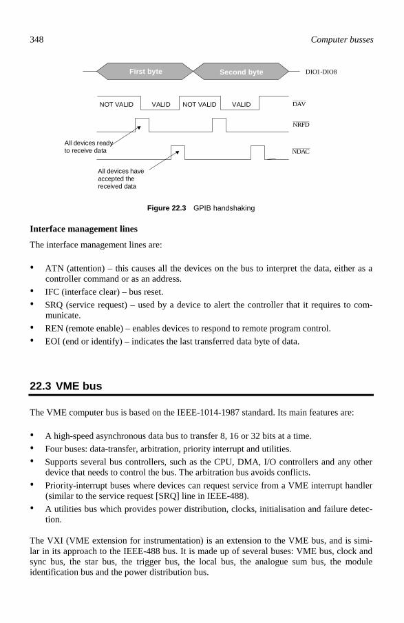
348 Computer busses
DAV
NRFD
NDAC
NOT VALID VALID NOT VALID VALID
All devices readyto receive data
All devices haveaccepted thereceived data
First byte Second byte DIO1-DIO8
Figure 22.3 GPIB handshaking
Interface management lines
The interface management lines are: • ATN (attention) – this causes all the devices on the bus to interpret the data, either as a
controller command or as an address. • IFC (interface clear) – bus reset. • SRQ (service request) – used by a device to alert the controller that it requires to com-
municate. • REN (remote enable) – enables devices to respond to remote program control. • EOI (end or identify) – indicates the last transferred data byte of data.
22.3 VME bus
The VME computer bus is based on the IEEE-1014-1987 standard. Its main features are: • A high-speed asynchronous data bus to transfer 8, 16 or 32 bits at a time. • Four buses: data-transfer, arbitration, priority interrupt and utilities. • Supports several bus controllers, such as the CPU, DMA, I/O controllers and any other
device that needs to control the bus. The arbitration bus avoids conflicts. • Priority-interrupt buses where devices can request service from a VME interrupt handler
(similar to the service request [SRQ] line in IEEE-488). • A utilities bus which provides power distribution, clocks, initialisation and failure detec-
tion. The VXI (VME extension for instrumentation) is an extension to the VME bus, and is simi-lar in its approach to the IEEE-488 bus. It is made up of several buses: VME bus, clock and sync bus, the star bus, the trigger bus, the local bus, the analogue sum bus, the module identification bus and the power distribution bus.

IEEE-488,VME and VXI 349
The VXI bus is intended for rack-mounted devices; each slot can take a module that is 30 mm (larger modules can take up more than one slot). Figure 22.4 shows the different sizes of modules that can be used with the VXI bus. Modules stand on edge, with cooling holes at the top and bottom edge of each module.
VME (A size)100x160mm
VME (B size)233x160mm
VXI (C size)233x340mm
VXI (D size)366x340mm
Figure 22.4 VMI module sizes
22.4 VXI bus
The VXI has several buses. These buses are global, unique or private. A global bus is a com-mon bus that connects to all of the cards. A private bus is used for local communications between a set of cards, and a unique bus provides additional, named signal lines. The buses can be grouped as follows: • Global – VME computer bus, trigger bus, analogue sum bus and power distribution bus. • Private – local bus. • Unique – star bus.
22.4.1 Clock and synchronisation bus
This bus contains two clocks and a clock synchronisation signal. One clock operates at 10 MHz, and the other is at 100 MHz, and these are accompanied by a sync signal. Each of the clocks uses ECL (emitter-coupled logic) and are buffered on the backplane, as illustrated in Figure 22.5.
22.4.2 Star bus
The star bus allows high-serial communications between each of the modules. It uses two high-performance ECL lines, named STARX and STARY. The bus is designed so that the path length between slot 0 and the other 12 slots is the same, and gives a maximum delay of 5 ns between slot 0 and any other module, as illustrated in Figure 22.6.

350 Computer busses
Slot 0 (Generates bus clocks)
Slot 1
Slot 2
Bus plane contains ECL buffers forclock distribution
Slot 12
Figure 22.5 VMI clock distribution
Slot 0
Slot 1
Slot 2Slot 3
Slot 12STARXSTARY
Equaldistancebetween allthe slots andslot 0
Figure 22.6 VMI clock distribution
22.4.3 Trigger bus
The trigger bus is a general-purpose logic bus that can be used for triggering, handshaking, clocking or data transmission. It uses eight TTL trigger lines and six ECL trigger lines.
22.4.4 Local bus
The local bus is used for intercommunication between two or more modules that does not use a global bus. It has 72 lines on each module, which are partitioned into 36 lines on each side of the module, as illustrated in Figure 22.7. The purpose of the bus is to decrease the need for jumpers between modules and to provide local communications between two or more mod-ules without using a global bus. For example, two cards could be placed in consecutive sock-ets and communicate with each other using the right-hand side pins on left-most card and the left-hand side pins on the right-most card.

IEEE-488,VME and VXI 351
Slot 1 Slot 2 Slot 3 Slot 4
Slot 0 Slot 5
P2 has2×12 lines
P3 has2×24 lines
Figure 22.7 Local bus backplane
22.4.5 Analogue SUMBUS
The Analogue SUMBUS provides for an analogue-summing node for all connected modules. It is possible for each module to drive the summing line using an analogue current source. Every module can also read from this line, using a high-impedance receiver. It is typically used to generate a complex waveform, where one or more modules can each provide a part of the waveform. For example, three modules could each provide a single frequency which are then summated onto the SUMBUS.
22.4.6 Module identification bus
This bus provides for an identification of the connected modules. It uses 12 identification wires which all connect to slot 0, and then one connection to each of the other slots. If a module is plugged into a slot, then it provides a ground connection for the module identifica-tion line, otherwise it will be an open circuit. This allows for quick system configuration at start-up and aids in diagnostics. Typically the module in slot 0 will scan the bus when it is started, if a module that is connected fails to communicate, the device in slot 0 may display an error for that device.
22.4.7 Power bus
The power bus provides: • Up to 268 W for each module. • Voltages of +5 V, +12 V, –12 V and +5V standby (battery backup) from the VME bus. • Voltages of +24 V and –24 V for analogue circuits for the VXI bus. • ECL voltages of –5.2 V and –2 V for ECL.

352 Computer busses
22.5 Exercises
22.5.1 What does GPIB standard for: (a) General-purpose interrupt bus (b) General-programmable interface bus (c) General-purpose interface bus (d) General-programmable interrupt bus 22.5.2 Which international specification defines the GPIB: (a) IEEE-488 (b) RS-486 (c) IEE-488 (d) GP-IB 22.5.3 How many data bits can be transferred over the IEEE-488 bus, at a time: (a) 8 (b) 16 (c) 32 (d) 64 22.5.4 An oscilloscope is likely to be which of the following GPIB function types: (a) Talker (b) Listener (c) Priority generator (d) Controller 22.5.5 A temperature instrument device is likely to be which of the following GPIB func-
tion types: (a) Talker (b) Listener (c) Priority generator (d) Controller 22.5.6 A data acquisition/controller PC is likely to be which of the following GPIB func-
tion types: (a) Talker (b) Listener (c) Priority generator (d) Controller 22.5.7 What is the function of the DAV handshaking line: (a) It defines that all the devices have received the data (b) It identifies when all the devices are ready (c) It resets the bus (d) It defines valid data on the bus 22.5.8 What is the function of the NDAC handshaking line: (a) It defines that all the devices have received the data (b) It identifies when all the devices are ready (c) It resets the bus

IEEE-488,VME and VXI 353
(d) It defines valid data on the bus 22.5.9 What is the function of the NDFD handshaking line: (a) It defines that all the devices have received the data (b) It identifies when all the devices are ready (c) It resets the bus (d) It defines valid data on the bus 22.5.10 Define the operation of the handshaking lines on the IEEE-488 bus. 22.5.11 Define the actions of talkers, listeners and controllers on an IEEE-488 bus. Give
examples of each type of device. 22.5.12 The IEEE-488 bus is a common bus, where all the devices connect to each of the
signal lines. Why are most of the handshaking lines active low?
22.6 Notes from the author
This chapter has covered one of the most simple busses, the IEEE-488 bus, and one of the most complex ones, the VME bus. So, why did I include them in a single chapter. Well, I cheated a little, because they didn’t really merit a chapter of their own, so I merged them (I’m sure I’ll receive lots of e-mails complaining about this, so I’ll give them both a chapter of their own in the second edition, if they both still exist and if I’m allowed a second edition). The IEEE-488 is a beautifully designed bus, which is well supported by software ven-dors, and is easy to set up. It will basically run quietly for many years without requiring any intervention by the user. The connector and cable are very well designed and can stand a great deal of abuse. It has typically been used a standard interface for instrumentation, but the growth of the serial busses is likely to reduce its importance. And what can I say about the VME bus. Oh boy, it’s complex. Its little brother, the VXI is a little less complex, but still is an extremely powerful and flexible bus for building modular instrumentation systems. Unfortunately it suffers from being too flexible and can be complex to write software for. The popularity of the PCI bus, and especially the CompactPCI bus (the PCI bus for modular systems) is overtaking the VXI bus.
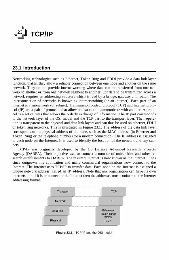
TCP/IP
23.1 Introduction
Networking technologies such as Ethernet, Token Ring and FDDI provide a data link layer function; that is, they allow a reliable connection between one node and another on the same network. They do not provide internetworking where data can be transferred from one net-work to another or from one network segment to another. For data to be transmitted across a network requires an addressing structure which is read by a bridge, gateway and router. The interconnection of networks is known as internetworking (or an internet). Each part of an internet is a subnetwork (or subnet). Transmission control protocol (TCP) and Internet proto-col (IP) are a pair of protocols that allow one subnet to communicate with another. A proto-col is a set of rules that allows the orderly exchange of information. The IP part corresponds to the network layer of the OSI model and the TCP part to the transport layer. Their opera-tion is transparent to the physical and data link layers and can thus be used on ethernet, FDDI or token ring networks. This is illustrated in Figure 23.1. The address of the data link layer corresponds to the physical address of the node, such as the MAC address (in Ethernet and Token Ring) or the telephone number (for a modem connection). The IP address is assigned to each node on the Internet. It is used to identify the location of the network and any sub-nets. TCP/IP was originally developed by the US Defense Advanced Research Projects Agency (DARPA). Their objective was to connect a number of universities and other re-search establishments to DARPA. The resultant internet is now known as the Internet. It has since outgrown this application and many commercial organizations now connect to the Internet. The Internet uses TCP/IP to transfer data. Each node on the Internet is assigned a unique network address, called an IP address. Note that any organisation can have its own internets, but if it is to connect to the Internet then the addresses must conform to the Internet addressing format.
Transport
Network
Data link
Physical
TCP
IP
Ethernet/Token Ring/
FDDI/ISDN
Figure 23.1 TCP/IP and the OSI model
23

356 Computer busses
The ISO have adopted TCP/IP as the basis for the standards relating to the network and transport layers of the OSI model. This standard is known as ISO-IP. Most currently avail-able systems conform to the IP addressing standard. Common applications that use TCP/IP communications are remote login and file transfer. Typical programs used in file transfer and login over TCP communication are ftp for file transfer program and telnet which allows remote log into another computer. The ping program determines if a node is responding to TCP/IP communications.
23.2 TCP/IP gateways and hosts
TCP/IP hosts are nodes which communicate over interconnected networks using TCP/IP communications. A TCP/IP gateway node connects one type of network to another. It con-tains hardware to provide the physical link between the different networks and the hardware and software to convert frames from one network to the other. Typically, it converts a Token Ring MAC layer to an equivalent Ethernet MAC layer, and vice versa. A router connects a network of a similar type to another of the same kind through a point-to-point link. The main operational difference between a gateway, a router, and a bridge is that for a Token Ring and Ethernet network, the bridge uses the 48-bit MAC address to route frames, whereas the gateway and router use the IP network address. As an analogy to the public telephone system, the MAC address would be equivalent to a randomly assigned tele-phone number, whereas the IP address would contain the information on where the telephone is logically located, such as which country, area code, and so on. Figure 23.2 shows how a gateway (or router) routes information. It reads the frame from the computer on network A, and reads the IP address contained in the frame and makes a decision whether it is routed out of network A to network B. If it does then it relays the frame to network B.
23.3 Function of the IP protocol
The main functions of the IP protocol are to: • Route IP data frames (which are called Internet datagrams) around an internet. The IP
protocol program running on each node knows the location of the gateway on the net-work. The gateway must then be able to locate the interconnected network. Data then passes from node to gateway through the Internet.
• Fragment the data into smaller units, if it is greater than a given amount (64 kB). • Report errors – when a datagram is being routed or is being reassembled an error can
occur. If this happens then the node that detects the error reports back to the source node. Datagrams are deleted from the network if they travel through the network for more than a set time. Again, an error message is returned to the source node to inform it that the in-ternet routing could not find a route for the datagram or that the destination node, or net-work, does not exist.

TCP/IP 357
Physical
Data link
Network
Transport
Ethernet, Token Ring,
FDDI modem
IP
TCP
Convertor to Ethernet,
Token Ring, FDDI
modem
IP
Ethernet, Token Ring,
FDDI modem
IP
TCP Internet gateway
Network A Network B
Figure 23.2 Internet gateway layers
23.4 Internet datagram
The IP protocol is an implementation of the network layer of the OSI model. It adds a data header onto the information passed from the transport layer, the resultant data packet is known as an internet datagram. The header contains information such as the destination and source IP addresses, the version number of the IP protocol and so on. Figure 23.3 shows its format.
1 2 3 4 5 6 7 8 9 10 11 12 13 14 15 16
Version Header length Type of service
Total length
Identification
Fragment offset
Protocol
Header checksum
Source IP address
Time-to-live
Destination IP address
0 D M
Options
Data (less than 64 kB)
Hea
der
Figure 23.3 Internet datagram format and contents

358 Computer busses
The datagram can contain up to 65 536 bytes (64 kB) of data. If the data to be transmitted is less than, or equal to, 64 kB, then it is sent as one datagram. If it is more than this then the sender splits the data into fragments and sends multiple datagrams. When transmitted from the source each datagram is routed separately through the internet and the received fragments are finally reassembled at the destination. The fields in the IP datagram are: • Version. The TCP/IP version number helps gateways and nodes interpret the data unit
correctly. Differing versions may have a different format. Most current implementations will have a version number of four (IPv4).
• Type of service. The type of service bit field is an 8-bit bit pattern in the form
PPPDTRXX, where PPP defines the priority of the datagram (from 0 to 7). The precedence levels are: 111 (network control) 110 (Internetwork control) 101 (CRITIC/ECP) 100 (flash override) 011 (flash) 010 (immediate) 001 (priority) 000 (routine)
D sets a low delay service (0 = normal delay, 1 = low delay). T sets high throughput (0 = normal throughput, 1 = high throughput). R sets high reliability (0 = normal reliability, 1 = high reliability). The XX bits are currently not used (and set to 00).
• Header length (4 bits). The header length defines the size of the data unit in multi-
plies of four bytes (32 bits). The minimum length is five bytes and the maximum is 65 536 bytes. Padding bytes fill any unused spaces.
• Identification (16 bits). A value which is assigned by the sender to aid the assembly of the frames of a datagram.
• D and M bits. A gateway may route a datagram and split it into smaller fragments. The D bit informs the gateway that it should not fragment the data and thus it signifies that a re-ceiving node should receive the data as a single unit or not at all. The M bit is the ‘more fragments’ bit and is used when data is split into fragments. The fragment offset contains the fragment number. The bit settings are:
D (don’t fragment) – 0 = may fragment, 1 = don’t fragment. M (last fragment) – 0 = last fragment, 1 = more fragments.
• Fragment offset (13 bits). Indicates which datagram this fragment belongs to. The frag-ment offset is measured in units of eight bytes (64 bits). The first fragment has an offset of zero.
• Time-to-live (8 bits). A datagram could propagate through the internet indefinitely. To
prevent this, the 8-bit time-to-live value is set to the maximum transit time in seconds and is set initially by the source IP. Each gateway then decrements this value by a defined amount. When it becomes zero the datagram is discarded. It also defines the maximum

TCP/IP 359
amount of time that a destination IP node should wait for the next datagram fragment. • Protocol (8 bits). Different IP protocols can be used on the datagram. The 8-bit proto-
col field defines the type to be used. A full list is given later in Table 23.5 (Section 23.16.1). Typical values are: 1 = ICMP and 6 = TCP.
• Header checksum (16 bits). The header checksum contains a 16-bit pattern for error
detection. As values within the header change from gateway to gateway (such as the time-to-live field), it must be recomputed every time the IP header is processed. The al-gorithm is: The 16-bit 1’s complement of the 1’s complement sum of all the 16-bit words in the header. When calculating the checksum the header checksum field is assumed to be set to a zero.
• Source and destination IP addresses (32 bits). The source and destination IP
addresses are stored in the 32-bit source and destination IP address fields. • Options. The options field contains information such as debugging, error control and
routing information. Section 23.16.2 gives further information.
23.5 ICMP
Messages, such as control data, information data and error recovery data, are carried between Internet hosts using the Internet control message protocol (ICMP). These messages are sent with a standard IP header. Typical messages are: • Destination unreachable (message type 3) – sent by a host on the network to say that a
host is unreachable. The message can also include the reason the host cannot be reached. • Echo request/echo reply (message type 8 or 0) – used to check the connectivity between
two hosts. The ping command uses this message, where it sends an ICMP ‘echo request’ message to the target host and waits for the destination host to reply with an ‘echo reply’ message.
• Redirection (message type 5) – sent by a router to a host that is requesting its routing ser-vices. This helps to find the shortest path to a desired host.
• Source quench (message type 4) – used when a host cannot receive any more IP packets at the present (or reduce the flow).
An ICMP message is sent within an IP header, with the version field, source and destination IP addresses, and so on. The type of service field is set to a 0 and the protocol field is set to a 1 (which identifies ICMP). After the IP header, follows the ICMP message, which starts with three fields, as per Figure 23.4. The message type has eight bits and identifies the type of message, as given in Table 23.1. The code fields are also eight bits long and a checksum field is 16 bits long. The checksum is the 1’s complement of the 1’s complement sum of all 16-bit words in the header (the checksum field is assumed to be zero in the addition). The information after this field depends on the type of message, such as:

360 Computer busses
• For echo request and reply, the message header is followed by an 8-bit identifier, then an 8-bit sequence number followed by the original IP header.
• For destination unreachable, source quelch and time, the message header is followed by 32 bits which are unused and then the original IP header.
• For timestamp request, the message header is followed by a 16-bit identifier, then by a 16-bit sequence number, followed by a 32-bit originating timestamp.
1 2 3 4 5 6 7 8 9 10 11 12 13 14 15 16
Version Header length Value = 0 Total length
Identification Fragment offset
Time-to-live Value = 1 (ICMP) Header checksum Source IP address
Destination IP address
Options
D
IP packet header
0 M
IP packet header Type Code Checksum Additional information
8 bits 8 bits 16 bits
ICMP message
Figure 23.4 ICMP message format
Where: • Pointer (8-bit) – identifies the byte location of the parameter error in the original IP
header. For example, a value of 9 would identify the protocol field, and 12 would identify the source IP address field.
• Identifier (16-bit) – helps the matching of requests and replies (possibly set to zero). It can be used to identify a unique connection.
• Sequence number (16-bit) – helps in matching request and replies (possibly set to zero). • Timestamps (32-bit) –this is the time in milliseconds since midnight UT (universal time).
If this is not possible then it is anytime, as long as the high-order bit of the timestamp is set to a 1 to indicate that it is non-standard time.
• Gateway address (32-bit) – the address of the gateway to which network traffic specified in the original datagram should be sent to.
• Internet header + 64 bits of data datagram – this is the original IP header and the first 64 byte of the data part. It is used by the host to match the match to the required high-level application (such as TCP port values).

TCP/IP 361
Table 23.1 Message type field value
Value Description Code field Additional information 0 Echo reply message 0
16-bit identifier 16-bit sequence number
3 Destination Unreachable
0 = net unreachable 1 = host unreachable 2 = protocol unreachable 3 = port unreachable 4 = fragmentation needed
and D bit set 5 = source route failed
32 bits unused. Internet header + 64 bits of original data datagram
4 Source quench message
0
32 bits unused. Internet header + 64 bits of original data datagram
5 Redirect message 0 = redirect datagram for the network
1 = redirect datagram for the host
2 = redirect datagram for the type of service and network
3 = redirect datagram for the type of service and host
32 bits gateway address. Internet header + 64 bits of original data datagram
8 Echo request 0
11 Time-to-live exceeded
0 = time-to-live exceeded in transit
1 = fragment reassembly time exceeded
32 bits unused. Internet header + 64 bits of original data datagram
12 Parameter problem 0 = pointer indicates the error
8-bit pointer. 24 bits unused. Internet header + 64 bits of original data datagram
13 Timestamp request 0
16-bit identifier 16-bit sequence number 32-bit originate timestamp 32-bit receive timestamp 32-bit transmit timestamp
14 Timestamp reply 0
As above
15 Information request 0 16-bit identifier 16-bit sequence number
16 Information reply 0 As above
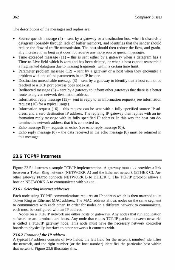
362 Computer busses
The descriptions of the messages and replies are: • Source quench message (4) – sent by a gateway or a destination host when it discards a
datagram (possibly through lack of buffer memory), and identifies that the sender should reduce the flow of traffic transmission. The host should then reduce the flow, and gradu-ally increase it, as long as it does not receive any more source quench messages.
• Time exceeded message (11) – this is sent either by a gateway when a datagram has a Time-to-Live field which is zero and has been deleted, or when a host cannot reassemble a fragmented datagram due to missing fragments, within a certain time limit.
• Parameter problem message (12) – sent by a gateway or a host when they encounter a problem with one of the parameters in an IP header.
• Destination unreachable message (3) – sent by a gateway to identify that a host cannot be reached or a TCP port process does not exist.
• Redirected message (5) – sent by a gateway to inform other gateways that there is a better route to a given network destination address.
• Information reply message (15)– sent in reply to an information request.( see information request (16) for a typical usage).
• Information request (16) – this request can be sent with a fully specified source IP ad-dress, and a zero destination IP address. The replying IP gateway then replies with an in-formation reply message with its fully specified IP address. In this way the host can de-termine the network address that it is connected to.
• Echo message (8) – requests an echo. (see echo reply message (0)). • Echo reply message (0) – the data received in the echo message (8) must be returned in
this message.
23.6 TCP/IP internets
Figure 23.5 illustrates a sample TCP/IP implementation. A gateway MERCURY provides a link between a Token Ring network (NETWORK A) and the Ethernet network (ETHER C). An-other gateway PLUTO connects NETWORK B to ETHER C. The TCP/IP protocol allows a host on NETWORK A to communicate with VAX01.
23.6.1 Selecting internet addresses
Each node using TCP/IP communications requires an IP address which is then matched to its Token Ring or Ethernet MAC address. The MAC address allows nodes on the same segment to communicate with each other. In order for nodes on a different network to communicate, each must be configured with an IP address. Nodes on a TCP/IP network are either hosts or gateways. Any nodes that run application software or are terminals are hosts. Any node that routes TCP/IP packets between networks is called a TCP/IP gateway node. This node must have the necessary network controller boards to physically interface to other networks it connects with.
23.6.2 Format of the IP address A typical IP address consists of two fields: the left field (or the network number) identifies the network, and the right number (or the host number) identifies the particular host within that network. Figure 23.6 illustrates this.

TCP/IP 363
VAX02
MOON
JUPITERMARS
MERCURY
PLUTO
OBERONVENUS
DIONE
VAX01
NETWORK A
NETWORK B
ETHER C
Figure 23.5 Example internet
Host numberNetwork number
[Host number]
Network A[Networknumber]
Network B[Networknumber]
[Host number]
[Host number]
Network C[Networknumber]
Figure 23.6 IP addressing over networks
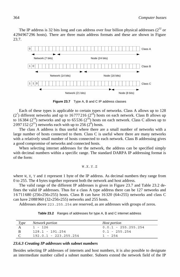
364 Computer busses
The IP address is 32 bits long and can address over four billion physical addresses (232 or 4294967296 hosts). There are three main address formats and these are shown in Figure 23.7.
0
Network (7 bits) Node (24 bits)
1 0
Network (14 bits) Node (16 bits)
1 1 0
Network (21 bits) Node (8 bits)
Class A
Class B
Class C
Figure 23.7 Type A, B and C IP address classes
Each of these types is applicable to certain types of networks. Class A allows up to 128 (27) different networks and up to 16777216 (224) hosts on each network. Class B allows up to 16384 (214) networks and up to 65536 (216) hosts on each network. Class C allows up to 2097152 (221) networks each with up to 256 (28) hosts. The class A address is thus useful where there are a small number of networks with a large number of hosts connected to them. Class C is useful where there are many networks with a relatively small number of hosts connected to each network. Class B addressing gives a good compromise of networks and connected hosts. When selecting internet addresses for the network, the address can be specified simply with decimal numbers within a specific range. The standard DARPA IP addressing format is of the form:
W.X.Y.Z where W, X, Y and Z represent 1 byte of the IP address. As decimal numbers they range from 0 to 255. The 4 bytes together represent both the network and host address. The valid range of the different IP addresses is given in Figure 23.7 and Table 23.2 de-fines the valid IP addresses. Thus for a class A type address there can be 127 networks and 16 711680 (256×256×255) hosts. Class B can have 16320 (64×255) networks and class C can have 2088960 (32×256×255) networks and 255 hosts. Addresses above 223.255.254 are reserved, as are addresses with groups of zeros.
Table 23.2 Ranges of addresses for type A, B and C internet address
Type Network portion Host portion A 1 - 126 0.0.1 - 255.255.254 B 128.1 - 191.254 0.1 - 255.254 C 192.0.1 - 223.255.254 1 - 254
23.6.3 Creating IP addresses with subnet numbers
Besides selecting IP addresses of internets and host numbers, it is also possible to designate an intermediate number called a subnet number. Subnets extend the network field of the IP

TCP/IP 365
address beyond the limit defined by the type A, B, C scheme. They allow a hierarchy of internets within a network. For example, it is possible to have one network number for a network attached to the internet, and various subnet numbers for each subnet within the net-work. This is illustrated in Figure 23.8.
Subnet numberNetwork number
Network A[Networknumber] Network C
[Networknumber]
Host number
Subnet A[Subnetnumber]
Subnet B[Subnetnumber]
Subnet C[Subnetnumber]
Subnet A[Subnetnumber]
Subnet B[Subnetnumber]
W.X.Y
W.X.Y
Figure 23.8 IP addresses with subnets
For an address W.X.Y.Z for a type A address W specifies the network and X the subnet. For type B the Y field specifies the subnet, as illustrated in Figure 23.9. To connect to a global network a number is normally assigned by a central authority. For the Internet network it is assigned by the network information center (NIC). Typically, on the Internet an organisation is assigned a type B network address. The first two fields of the ad-dress specify the organisation network, the third specifies the subnet within the organization and the final value specifies the host.
Subnet number(Y)
Network number(W.X)
Network A[Networknumber] Network C
[Networknumber]
W.X.Y.Z
Host number(Z)
Subnet A[Subnetnumber]
Subnet B[Subnetnumber]
Subnet C[Subnetnumber]
Subnet A[Subnetnumber]
Subnet B[Subnetnumber]
W.X
W.X.Y
W.X.Y
W.X.Y
W.X
W.X.Y
W.X.Y.Z
Figure 23.9 Internet addresses with subnets

366 Computer busses
23.6.4 Specifying subnet masks
If a subnet is used then a bit mask, or subnet mask, must be specified to show which part of the address is the network part and which is the host. The subnet mask is a 32-bit number that has 1’s for bit positions specifying the network and subnet parts and 0’s for the host part. A text file called hosts is normally used to set up the subnet mask. Table 23.3 shows example subnet masks.
Table 23.3 Default subnet mask for type A, B and C IP addresses
Address Type Default mask Class A 255.0.0.0
Class B 255.255.0.0
Class C and Class B with a subnet 255.255.255.0
To set up the default mask the following line is added to the hosts file.
Hosts file 255.255.255.0 defaultmask
23.7 Domain name system
An IP address can be defined in the form WWW.XXX.YYY.ZZZ, where XXX, YYY, ZZZ and WWW are integer values in the range 0 to 255. On the Internet, with Class B IP addresses, it is WWW.XXX.YYY that normally defines the subnet and ZZZ that defines the host. Such names may be difficult to remember. A better method is to use symbolic names rather than IP ad-dresses. Users and application programs can then use symbolic names rather than the IP ad-dresses. The directory network service on the Internet determines the IP address of the named destination user or application program. This has the advantage that users and appli-cation programs can move around the Internet and are not fixed to an IP address. An analogy relates to the public telephone service. A telephone directory contains a list of subscribers and their associated telephone numbers. If someone looks for a telephone number, first the user name is looked up and then the associated telephone number found. The telephone directory listing maps a user name (symbolic name) to an actual telephone number (the actual address). Table 23.4 lists some Internet domain assignments for World Wide Web (WWW) serv-ers. Note that domain assignments are not fixed and can change their corresponding IP ad-dresses, if required. The binding between the symbolic name and its address can thus change at any time.

TCP/IP 367
Table 23.4 Internet domain assignments for web servers
Web server Internet domain name Internet IP address NEC web.nec.com 143.101.112.6
Sony www.sony.com 198.83.178.11
Intel www.intel.com 134.134.214.1
IEEE www.ieee.com 140.98.1.1
University of Bath www.bath.ac.uk 136.38.32.1
University of Edinburgh www.ed.ac.uk 129.218.128.43
IEE www.iee.org.uk 193.130.181.10
University of Manchester www.man.ac.uk 130.88.203.16
23.8 Internet naming structure
The Internet naming structure uses labels separated by periods; an example is eece.napier.ac.uk. It uses a hierarchical structure where organisations are grouped into primary domain names. These are com (for commercial organisations), edu (for educational organisations), gov (for government organisations), mil (for military organisations), net (Internet network support centers) or org (other organisations). The primary domain name may also define the country in which the host is located, such as uk (United Kingdom), fr (France), and so on. All hosts on the Internet must be registered to one of these primary do-main names. The labels after the primary field describe the subnets within the network. For example in the address eece.napier.ac.uk, the ac label relates to an academic institution within the uk, napier to the name of the institution and eece the subnet within that organisation. An exam-ple structure is illustrated in Figure 23.10.
edu gov com mil usa uk fr
ac
ed bath napier man
eece cs mmseeece.napier.ac.uk
intel sony nec
wwwwww.eece.napier.ac.uk
Figure 23.10 Example domain naming

368 Computer busses
23.9 Domain name server
Each institution on the Internet has a host that runs a process called the domain name server (DNS). The DNS maintains a database called the directory information base (DIB) which contains directory information for that institution. When a new host is added, the system manager adds its name and its IP address. It can then access the Internet.
23.9.1 DNS program
The DNS program is typically run on a Linux-based PC with a program called named (lo-cated in /usr/sbin) with an information file of named.boot. To run the program the fol-lowing is used: /usr/bin/named -b /usr/local/adm/named/named.boot The following shows that the DNS program is currently running. $ ps -ax PID TTY STAT TIME COMMAND 295 con S 0:00 bootpd 35 con S 0:00 /usr/sbin/lpd 272 con S 0:00 /usr/sbin/named -b /usr/local/adm/named/named.boot 264 p 1 S 0:01 bash 306 pp0 R 0:00 ps -ax
In this case the data file named.boot is located in the /usr/local/adm/named directory. A sample named.boot file is /usr/local/adm/named - soabasefile eece.napier.ac.uk -main record of computer names net/net144 -reverse look-up database net/net145 “ “ net/net146 “ “ net/net147 “ “ net/net150 “ “ net/net151 “ “ This file specifies that the reverse look-up information on computers on the subnets 144, 145, 146, 147, 150 and 151 is contained in the net144, net145, net146, net147, net150 and net151 files, respectively. These are stored in the net subdirectory. The main file which contains the DNS information is, in this case, eece.napier.ac.uk. Whenever a new computer is added onto a network, in this case, the eece.napier.ac.uk file and the net/net1** (where ** is the relevant subnet name) are updated to reflect the changes. Finally, the serial number at the top of these data files is up-dated to reflect the current date, such as 19970321 (for 21st March 1997). The DNS program can then be tested using nslookup; For example, $ nslookup Default Server: ees99.eece.napier.ac.uk Address: 146.176.151.99 > src.doc.ic.ac.uk Server: ees99.eece.napier.ac.uk Address: 146.176.151.99 Non-authoritative answer:

TCP/IP 369
Name: swallow.doc.ic.ac.uk Address: 193.63.255.4 Aliases: src.doc.ic.ac.uk
23.10 Bootp protocol
The bootp protocol allocates IP addresses to computers based on a table of network card MAC addresses. When a computer is first booted, the bootp server interrogates its MAC ad-dress and then looks up the bootp table for its entry. It then grants the corresponding IP ad-dress to the computer. The computer then uses it for connections.
23.10.1 Bootp program
The bootp program is typically run on a Linux-based PC with the bootp program. The fol-lowing shows that the bootp program is currently running on a computer: $ ps -ax
PID TTY STAT TIME COMMAND 1 con S 0:06 init 31 con S 0:01 /usr/sbin/inetd 14142 con S 0:00 bootpd -d 1 35 con S 0:00 /usr/sbin/lpd 49 p 3 S 0:00 /sbin/agetty 38400 tty3 14155 pp0 R 0:00 ps -ax 10762 con S 0:18 /usr/sbin/named -b /usr/local/adm/named/named.boot
For the bootp system to operate then a table is required that reconciles the MAC addresses of the card to an IP address. In the previous example this table is contained in the bootptab file which is located in the /etc directory. The following file gives an example bootptab: Contents of bootptab file
# /etc/bootptab: database for bootp server # Blank lines and lines beginning with '#' are ignored. # Legend: # first field -- hostname # (may be full domain name and probably should be) # hd -- home directory # bf -- bootfile # cs -- cookie servers # ds -- domain name servers # gw -- gateways # ha -- hardware address # ht -- hardware type # im -- impress servers # ip -- host IP address # lg -- log servers # lp -- LPR servers # ns -- IEN-116 name servers # rl -- resource location protocol servers # sm -- subnet mask # tc -- template host (points to similar host entry) # to -- time offset (seconds) # ts -- time servers

370 Computer busses
# #hostname:ht=1:ha=ether_addr_in_hex:ip=ip_addr_in_dec:tc=allhost: .default150:\ :hd=/tmp:bf=null:\ :ds=146.176.151.99 146.176.150.62 146.176.1.5:\ :sm=255.255.255.0:gw=146.176.150.253:\ :hn:vm=auto:to=0: .default151:\ :hd=/tmp:bf=null:\ :ds=146.176.151.99 146.176.150.62 146.176.1.5:\ :sm=255.255.255.0:gw=146.176.151.254:\ :hn:vm=auto:to=0: pc345: ht=ethernet: ha=0080C8226BE2: ip=146.176.150.2: tc=.default150: pc307: ht=ethernet: ha=0080C822CD4E: ip=146.176.150.3: tc=.default150: pc320: ht=ethernet: ha=0080C823114C: ip=146.176.150.4: tc=.default150: pc331: ht=ethernet: ha=0080C823124B: ip=146.176.150.5: tc=.default150: pc401: ht=ethernet: ha=0080C82379F7: ip=146.176.150.6: tc=.default150: pc404: ht=ethernet: ha=0080C8238369: ip=146.176.150.7: tc=.default150: pc402: ht=ethernet: ha=0080C8238467: ip=146.176.150.8: tc=.default150: : : pc460: ht=ethernet: ha=0000E8C7BB63: ip=146.176.151.142: tc=.default151: pc414: ht=ethernet: ha=0080C8246A84: ip=146.176.151.143: tc=.default151: pc405: ht=ethernet: ha=0080C82382EE: ip=146.176.151.145: tc=.default151:
The format of the file is: #hostname:ht=1:ha=ether_addr_in_hex:ip=ip_addr_in_dec:tc=allhost: where hostname is the hostname, the value defined after ha= is the Ethernet MAC address, the value after ip= is the IP address and the name after the tc= field defines the host infor-mation script. For example: pc345: ht=ethernet: ha=0080C8226BE2: ip=146.176.150.2: tc=.default150; defines the hostname of pc345, ethernet indicates it is on an Ethernet network, and shows its IP address is 146.176.150.2. The MAC address of the computer is 00:80:C8: 22:6B:E2 and it is defined by the script .default150. This file defines a subnet of 255.255.255.0 and has associated DNS of 146.176.151.99 146.176.150.62 146.176.1.5 and uses the gateway at 146.176.150.253

TCP/IP 371
23.11 Example network
A university network is shown in Figure 23.11. The connection to the outside global Internet is via the Janet gateway node and its IP address is 146.176.1.3. Three subnets, 146.176.160, 146.176.129 and 146.176.151, connect the gateway to departmental bridges. The Computer Studies bridge address is 146.176.160.1 and the Electrical De-partment bridge has an address 146.176.151.254. The Electrical Department bridge links, through other bridges, to the subnets 146.176.144, 146.176.145, 146.176.147, 146.176.150 and 146.176.151. The main bridge (Figure 23.12) into the department connects to two Ethernet networks of PCs (subnets 146.176.150 and 146.176.151) and to another bridge (Bridge 1). Bridge 1 connects to the subnet 146.176.144. Subnet 146.176.144 connects to workstations and X-terminals. It also connects to the gateway Moon that links the Token Ring subnet 146.176.145 with the Ethernet subnet 146.176.144. The gateway Oberon, on the 146.176.145 subnet, connects to an Ethernet link 146.176.146. This then connects to the gateway Dione that is also connected to the Token Ring subnet 146.176.147. The topology of the Electrical Department network is shown in Figure 23.12. Each node on the network is assigned an IP address. The hosts file for the set-up in Figure 23.12 is shown next. For example the IP address of Mimas is 146.176.145.21 and for miranda it is 146.176.144.14. Notice that the gateway nodes, Oberon, Moon and Dione, all have two IP addresses.
GlobalInternet
ComputerStudiesbridge
ElectricalDepartmentbridge
146.176.160
146.176.151
146.176.151.254
146.176.144
146.176.145
146.176.147
146.176.150
146.176.151
Janetgateway146.176.1.3
146.176.160.1
146.176.129146.176Mechanical
Departmentbridge146.176.129.1
Figure 23.11 A university network
Contents of host file 146.176.1.3 janet 146.176.144.10 hp 146.176.145.21 mimas 146.176.144.11 mwave 146.176.144.13 vax 146.176.144.14 miranda 146.176.144.20 triton 146.176.146.23 oberon 146.176.145.23 oberon 146.176.145.24 moon

372 Computer busses
146.176.144.24 moon 146.176.147.25 uranus 146.176.146.30 dione 146.176.147.30 dione 146.176.147.31 saturn 146.176.147.32 mercury 146.176.147.33 earth 146.176.147.34 deimos 146.176.147.35 ariel 146.176.147.36 neptune 146.176.147.37 phobos 146.176.147.39 io 146.176.147.40 titan 146.176.147.41 venus 146.176.147.42 pluto 146.176.147.43 mars 146.176.147.44 rhea 146.176.147.22 jupiter 146.176.144.54 leda 146.176.144.55 castor 146.176.144.56 pollux 146.176.144.57 rigel 146.176.144.58 spica 146.176.151.254 cubridge 146.176.151.99 bridge_1 146.176.151.98 pc2 ::::: 146.176.151.71 pc29 146.176.151.70 pc30 146.176.151.99 ees99 146.176.150.61 eepc01 146.176.150.62 eepc02 255.255.255.0 defaultmask
146.176.144
pc2 pc3
Dione
Saturn
Mercury
Earth
Pluto
Venus
Titan
Io
Phobos
Neptune
Ariel
Rhea
+Demos+Uranus
Oberon
Moon
Mimas
HP
VAX
Miranda
Triton
Vega(X)
Rigel(X)
Mwave
Intel
Leda
Castor
Pollux
Spica
Token Ring networks
WorkstationEthernetnetwork
PC Ethernet network
ElectricalDepartmentbridge/router
146.176.151
146.176.150
146.176.146
146.176.145146.176.147
eepc02eepc01
Bridge1
Figure 23.12 Network topology for the Electrical Department network

TCP/IP 373
23.12 ARP
ARP (address resolution protocol) translates IP addresses to Ethernet addresses. This is used when IP packets are sent from a computer, and the Ethernet address is added to the Ethernet frame. A table look-up, called the ARP table, is used to translate the addresses. One column has the IP address and the other has the Ethernet address. The following is an example ARP table: IP address Ethernet address 146.176.150.2 00-80-C8-22-6BE2 146.176.150.3 00-80-C8-22-CD4E 146.176.150.4 00-80-C8-23-114C
A typical conversation is as follows: 1. Application sends an application message to TCP. 2. TCP sends the corresponding TCP message to the IP module. The destination IP address
is known by the application, the TCP module, and the IP module. 3. At this point the IP packet has been constructed and is ready to be given to the Ethernet
driver, but first the destination Ethernet address must be determined. 4. The ARP table is used to look up the destination Ethernet address. The sequence of determining the Ethernet address is as follows: 1. An ARP request packet with a broadcast Ethernet address (FF-FF-FF-FF-FF-FF) is
sent out on the network to every computer. Other typical Ethernet broadcast addresses are given in Section 23.16.3.
2. The outgoing IP packet is queued. 3. All the computers on the network segment read the broadcast Ethernet frame, and exam-
ine the Type field to determine if it is an ARP packet. If it is then it is passed to the ARP module.
4. If the IP address of a receiving station matches the IP address in the IP packet then it sends a response directly to the source Ethernet address.
5. The originator then receives the Ethernet frame and checks the Type field to determine if it an ARP packet. If it is then it adds the sender’s IP address and Ethernet address to its ARP table.
6. The IP packet can now be sent with the correct Ethernet address. Each computer has a separate ARP table for each of its Ethernet interfaces.
23.13 IP multicasting
Many applications of modern communications require the transmission of IP datagrams to multiple hosts. Typical applications are video conferencing, remote teaching and so on. This is supported by IP multicasting, where a host group is identified by a single IP address. The

374 Computer busses
main parameters of IP multicasting are: • The group membership is dynamic. • Hosts may join and leave the group at any time. • There is also no limit to the location or number of members in a host group. • A host may be a member of more than one group at a time. • A host group may be permanent or transient. Permanent groups are well-known and are
administratively assigned a permanent IP address. The group is then dynamically associ-ated with this IP address. IP multicast addresses that are not reserved to permanent groups are available for dynamic assignment to transient groups.
• Multicast routers forward IP multicast datagrams into the Internet.
23.13.1 Group addresses
A special group of addresses are assigned to multicasting. These are known as Class D ad-dresses, and they begin with 1110 as their starting 4 bits (Class E addresses with the upper bits of 1111 are reserved for future uses). The Class D addresses thus range from
224.0.0.0 (11100000 00000000 00000000 00000000) 239.255.255.255 (11101111 11111111 11111111 11111111)
The address 224.0.0.0 is reserved. 224.0.0.1 is also assigned to the permanent group of all IP hosts (including gateways), and is used to address all multicast hosts on the directly con-nected network. Reserved and allocated addresses are:
224.0.0.0 Reserved 224.0.0.1 All systems on current subnet 224.0.0.2 All routers on current subnet 224.0.0.3 Unassigned 224.0.0.4 DVMRP routers 224.0.0.5 OSPFIGP all routers 224.0.0.6 OSPFIGP designated routers 224.0.0.7 ST routers 224.0.0.8 ST hosts 224.0.0.9 RIP2 routers 224.0.0.10–224.0.0.255 Unassigned 224.0.1.0 VMTP managers group 224.0.1.1 NTP network time protocol 224.0.1.2 SGI-dogfight 224.0.1.3 Rwhod 224.0.1.4 VNP 224.0.1.5 Artificial horizons–aviator 224.0.1.6 NSS–name service server 224.0.1.7 AUDIONEWS–audio news multicast 224.0.1.8 SUN NIS+ information service 224.0.1.9 MTP multicast transport protocol 224.0.1.10–224.0.1.255 Unassigned 224.0.2.1 rwho group (BSD) (unofficial) 224.0.2.2 SUN RPC PMAPPROC_CALLIT 224.0.3.0–224.0.3.255 RFE generic service 224.0.4.0–224.0.4.255 RFE individual conferences

TCP/IP 375
224.1.0.0–224.1.255.255 ST multicast groups 224.2.0.0–224.2.255.255 Multimedia conference calls 232.x.x.x VMTP transient groups
All the above addresses are listed in the domain name service under MCAST.NET and 224.IN-ADDR.ARPA. On an Ethernet or IEEE 802 network, the 23 low-order bits of the IP multicast address are placed in the low-order 23 bits of the Ethernet or IEEE 802 net multi-cast address.
23.13.2 Conformance
There are three levels of conformance: • Level 0, no IP multicasting support – in this, a Level 0 host ignores, or deletes, all Class
D addressed datagrams. • Level 1, sending support, but no receiving – in this, a Level 1 host can send multicast
datagrams, but cannot receive them. • Level 2, Full multicasting support – in this, a Level 2 host can send and receive IP multi-
casting. It also requires the implementation of the Internet group management protocol (IGMP).
23.14 Exercises
23.14.1 Which OSI layer does the IP layer correspond to: (a) Data link (b) Network (c) Transport (d) Session 23.14.2 Which OSI layer does the TCP layer correspond to: (a) Data link (b) Network (c) Transport (d) Session 23.14.3 Which IP version do most TCP/IP hosts use: (a) Version 2 (b) Version 4 (c) Version 5 (d) Version 6 23.14.4 How much data can be carried within an IP datagram: (a) 64 kB (b) 128 kB (c) 256 kB (d) Unlimited 23.14.5 How many IP addresses are possible: (a) 1048 576 (b) 16 777 216 (c) 4 294 967 296 (d) 3.402 823 669×1038

376 Computer busses
23.14.6 How are IP datagrams deleted from the network: (a) They are deleted when the time-to-live field becomes zero. (b) They are never deleted, and will always be delivered. (c) They are buffered on intermediate systems, and then deleted after a given time. (d) They are returned to the originator if they are not deleted, and the originator either resends them or deletes them. 23.14.7 Which of the following is a Class A IP address: (a) 12.1.14.12 (b) 146.176.151.130 (c) 194.50.100.1 (d) 224.50.50.1 23.14.8 Which of the following is a Class D IP address: (a) 12.1.14.12 (b) 146.176.151.130 (c) 194.50.100.1 (d) 224.50.50.1 23.14.9 What are Class D IP addresses used for: (a) Dynamic IP addressing (b) Testing networks (c) Static IP addressing (d) Multicasting 23.14.10 Which of the following is the country domain for Germany: (a) ge (b) de (c) dr (d) gy 23.14.11 Which service allows hosts to determine the IP address for a given domain name: (a) TCP (b) ICMP (c) ARP (d) DNS 23.14.12 Which protocol is used by a node to determine the Ethernet address to a host with
a given IP address: (a) TCP (b) ICMP (c) ARP (d) DNS 23.14.13 Which Ethernet address is used for broadcast messages: (a) FF-FF-FF-FF-FF-FF (b) 11-11-11-11-11-11-11 (c) 00-00-00-00-00-00 (d) AA-AA-AA-AA-AA-AA 23.14.14 Outline how ARP uses the broadcast address and the type field to identify that an
ARP request is being transmitted. Also, discuss a typical ARP conversation. 23.14.15 Outline how the protocol is identified in the IP header. Discuss how the format of
the data after the header differs with different protocols (such as TCP and ICMP).

TCP/IP 377
23.14.16 Explain how ICMP and the options field would be used to determine the following information:
(i) Whether a destination node is responding to TCP/IP communications. (ii) The route to a destination node. (iii) The route to a destination node, with the time delay between each gateway. 23.14.17 Explain how the Options field can be used to set the route that a datagram can
take. 23.14.18 Determine the IP addresses, and their type (i.e. class A, B or C), of the following
32-bit addresses: (i) 10001100.01110001.00000001.00001001 (ii) 01000000.01111101.01000001.11101001 (iii) 10101110.01110001.00011101.00111001 23.14.19 Determine the countries which use the following primary domain names: (a) de (b) nl (c) it (d) se (e) dk (f) sg (g) ca (h) ch (i) tr (j) jp (k) au Determine some other domain names. 23.14.20 For a known TCP/IP network determine the names of the nodes and their Internet
addresses. 23.14.21 For a known TCP/IP network determine how the DNS is implemented and how IP
addresses are granted. 23.14.22 If a subnet mask on a Class B network is 255.255.240.0, show that there can be 16
connected networks, each with 4095 nodes on a Class B network.
23.15 Notes from the author
Which two people have done more for world unity than anyone else? Well, Prof. TCP and Dr. IP must be somewhere in the Top 10. They have done more to unify the world than all the diplomats in the world have. They do not respect national borders, time zones, cultures, in-dustrial conglomerates or anything like that. They allow the sharing of information around the world, and are totally open for anyone to use. Top marks to Prof. TCP and Dr. IP, the true champions of freedom and democracy. Many of the great inventions/developments of our time were things that were not really predicted, such as CD-ROMs, RADAR, silicon transistors, fibre optic cables, and, of course, the Internet. The Internet itself is basically an infrastructure of interconnected networks which run a common protocol. The nightmare of interfacing the many computer systems around the world was solved because of two simple protocols: TCP and IP. Without them the

378 Computer busses
Internet would not have evolved so quickly and possibly would not have occurred at all. TCP and IP are excellent protocols as they are simple and can be run over any type of network, on any type of computer system. The Internet is often confused with the World Wide Web (WWW), but the WWW is only one application of the Internet. Others include electronic mail (the No.1 application), file transfer, remote login and so on. The amount of information transmitted over networks increases by a large factor every year. This is due to local area networks, wide area networks and of course, traffic over the Internet. It is currently estimated that traffic on the Internet doubles every 100 days and that three people join the Internet every second. This means an eightfold increase in traffic over a whole year. It is hard to imagine such growth in any other technological area. Imagine if cars were eight times faster each year, or could carry eight times the number of passengers each year (and of course roads and driveways would have to be eight times larger each year).
23.16 Additional material
23.16.1 Assigned Internet protocol numbers
Table 23.5 outlines the values that are used in the protocol field of the IP header.
Table 23.5 Assigned Internet protocol numbers
Value Protocol Value Protocol 0 Reserved 18 Multiplexing 1 ICMP 19 DCN 2 IGMP (Internet group management) 20 TAC monitoring 3 Gateway-to-gateway 21–62 4 CMCC gateway monitoring message 63 Any local network 5 ST 64 SATNET and backroom EXPAK 6 TCP 65 MIT subnet support 7 UCL 66–68 Unassigned 8 EGP (exterior gateway protocol) 69 SATNET monitoring 9 Secure 70 Unassigned 10 BBN RCC monitoring 71 Internet Packet core utility 11 NVP 72–75 Unassigned 12 PUP 76 Backroom SATNET monitoring 13 Pluribus 77 Unassigned 14 Telenet 78 WIDEBAND monitoring 15 XNET 79 WIDEBAND EXPAK 16 Chaos 80–254 Unassigned 17 User datagram 255 Reserved
23.16.2 Options field in an IP header
The options field in an IP header is an optional field which may or may not appear in the header, and is also variable in length. It is a field which must be implemented by all hosts and gateways. There are two classes of option:
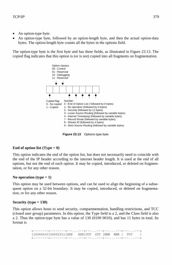
TCP/IP 379
• An option-type byte. • An option-type byte, followed by an option-length byte, and then the actual option-data
bytes. The option-length byte counts all the bytes in the options field. The option-type byte is the first byte and has three fields, as illustrated in Figure 23.13. The copied flag indicates that this option is (or is not) copied into all fragments on fragmentation.
Copied flag0 - No copied1 - Copied
Option classes00 - Control01 - Reserved10 - Debugging11 - Reserved
Number0 - End of Option List ( followed by 0 bytes)1 - No operation (followed by 0 bytes)2 - Security (followed by 11 bytes)3 - Loose Source Routing (followed by variable bytes)4 - Internet Timestamp (followed by variable bytes)7 - Record Route (followed by variable bytes)8 - Stream ID (followed by 4 bytes)9 - Strict Source Routing (followed by variable bytes)
Figure 23.13 Options-type byte
End of option list (Type = 0)
This option indicates the end of the option list, but does not necessarily need to coincide with the end of the IP header according to the internet header length. It is used at the end of all options, but not the end of each option. It may be copied, introduced, or deleted on fragmen-tation, or for any other reason.
No operation (type = 1)
This option may be used between options, and can be used to align the beginning of a subse-quent option on a 32-bit boundary. It may be copied, introduced, or deleted on fragmenta-tion, or for any other reason.
Security (type = 130)
This option allows hosts to send security, compartmentation, handling restrictions, and TCC (closed user group) parameters. In this option, the Type field is a 2, and the Class field is also a 2. Thus the option-type byte has a value of 130 (0100 0010), and has 11 bytes in total. Its format is +--------+--------+---...---+---...---+---...---+---...---+ |10000010|00001011|SSS SSS|CCC CCC |HHH HHH | TCC | +--------+--------+---...---+---...---+---...---+---...---+
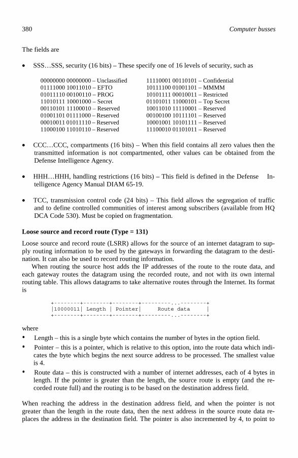
380 Computer busses
The fields are • SSS…SSS, security (16 bits) – These specify one of 16 levels of security, such as 00000000 00000000 – Unclassified 11110001 00110101 – Confidential 01111000 10011010 – EFTO 10111100 01001101 – MMMM 01011110 00100110 – PROG 10101111 00010011 – Restricted 11010111 10001000 – Secret 01101011 11000101 – Top Secret 00110101 11100010 – Reserved 10011010 11110001 – Reserved 01001101 01111000 – Reserved 00100100 10111101 – Reserved 00010011 01011110 – Reserved 10001001 10101111 – Reserved 11000100 11010110 – Reserved 11100010 01101011 – Reserved • CCC…CCC, compartments (16 bits) – When this field contains all zero values then the
transmitted information is not compartmented, other values can be obtained from the Defense Intelligence Agency.
• HHH…HHH, handling restrictions (16 bits) – This field is defined in the Defense In-
telligence Agency Manual DIAM 65-19. • TCC, transmission control code (24 bits) – This field allows the segregation of traffic
and to define controlled communities of interest among subscribers (available from HQ DCA Code 530). Must be copied on fragmentation.
Loose source and record route (Type = 131)
Loose source and record route (LSRR) allows for the source of an internet datagram to sup-ply routing information to be used by the gateways in forwarding the datagram to the desti-nation. It can also be used to record routing information. When routing the source host adds the IP addresses of the route to the route data, and each gateway routes the datagram using the recorded route, and not with its own internal routing table. This allows datagrams to take alternative routes through the Internet. Its format is +--------+--------+--------+---------...--------+ |10000011| Length | Pointer| Route data | +--------+--------+--------+---------...--------+ where • Length – this is a single byte which contains the number of bytes in the option field. • Pointer – this is a pointer, which is relative to this option, into the route data which indi-
cates the byte which begins the next source address to be processed. The smallest value is 4.
• Route data – this is constructed with a number of internet addresses, each of 4 bytes in length. If the pointer is greater than the length, the source route is empty (and the re-corded route full) and the routing is to be based on the destination address field.
When reaching the address in the destination address field, and when the pointer is not greater than the length in the route data, then the next address in the source route data re-places the address in the destination field. The pointer is also incremented by 4, to point to

TCP/IP 381
the next address. It is loose as the gateways are allowed to use any route to get to the next specified address in the routing table. It must be copied on fragmentation and occurs, at the most, once in a datagram.
Strict source and record route (Type = 137)
The SSRR is similar to the LSRR, but the routing must follow, exactly, the addresses in the routing table. It thus cannot use any intermediate routes to get to these addresses. Its format is +--------+--------+--------+---------...--------+ |10001001| Length | Pointer| Route data | +--------+--------+--------+---------...--------+
Record route (type = 7)
The record route option records the route of an internet datagram. It can thus be used by such utilities as Traceroute. Its format is +--------+--------+--------+---------...--------+ |00000111| Length | Pointer| Route data | +--------+--------+--------+---------...--------+ where • Length – this is a single byte which contains the number of bytes in the option field. • Pointer – this is a pointer, which is relative to this option, into the route data which indi-
cates the byte at which the next address should be added to. The smallest value is 4. • Route data – contains a list of the route which a datagram has taken. Each entry has 4
bytes. The originating host must reserve enough area for the total number of addresses in the routing table, as the size of this option does not change as it transverses over the Internet. If there is a problem adding the address then an ICMP Parameter Problem can be sent back to the source host.
It is not copied on fragmentation, and goes in the first fragment only. In addition, it occurs, at the most, once in a datagram.
Internet timestamp (type = 68)
The Internet timestamp option records a timestamp for each gateway along the route of a datagram. It allows the source host to trace the time that each part of the route takes. Its for-mat is +--------+--------+--------+--------+ |01000100| Length | Pointer|Ov |Flg| +--------+--------+--------+--------+ | internet address | +--------+--------+--------+--------+ | timestamp | +--------+--------+--------+--------+ | . | .
where

382 Computer busses
• Length. – is a single byte which contains the number of bytes in the option field (maxi-mum is 40).
• Pointer – this is a pointer, which is relative to this option, into the route data which indi-cates the byte at which the next timestamp should be added to. The smallest value is 5.
• Overflow (Ov) – this has four bits and holds the number of IP modules that cannot regis-ter timestamps due to lack of space.
• Flag (Flg) – this has four bits and defines the format of the timestamp. Valid values are:
0 – Store only the time stamps as 32-bit words. 1 – Store IP address followed by a time stamp. 3 – In this mode the IP addresses are specified in a table. A gateway only adds its time-
stamp if its IP address is in this table. • Timestamp – this is a 32-bit value for the number of milliseconds since midnight UT
(universal time). If this is not possible then it is any time, as long as the high-order bit of the timestamp is set to a 1 to indicate that it is non-standard time.
The originating host must reserve enough area for the total number of timestamps, as the size of this option does not change as it transverses over the Internet. If there is a problem adding the address then an ICMP parameter problem can be sent back to the source host. Initially the contents of the timestamp data area is either zero, or has IP addresses with zero time stamps. The timestamp area is full when the pointer is greater than the length. It is not copied on fragmentation, and goes in the first fragment only. Also, it occurs, at the most once in a datagram.
Stream identifier (type =136)
This option allows for a 16-bit SATNET stream identifier to be carried through networks that do not support the stream concept. Its format is +--------+--------+--------+--------+ |10001000|00000010| Stream ID | +--------+--------+--------+--------+
23.16.3 Ethernet multicast/broadcast addresses
The following is a list of typical Ethernet multicast addresses: Ethernet address Type field Usage 01-00-5E-00-00-00 0800 Internet multicast (RFC-1112) 01-80-C2-00-00-00 0802 Spanning tree (for bridges) 09-00-09-00-00-01 8005 HP probe 09-00-09-00-00-04 8005 HP DTC 09-00-1E-00-00-00 8019 Apollo DOMAIN 09-00-2B-00-00-03 8038 DEC lanbridge traffic monitor (LTM) 09-00-4E-00-00-02 8137 Novell IPX CF-00-00-00-00-00 9000 Ethernet configuration test protocol
The following is a list of typical Ethernet broadcast addresses: Ethernet address Type field Usage FF-FF-FF-FF-FF-FF 0600 XNS packets, hello or gateway search.

TCP/IP 383
FF-FF-FF-FF-FF-FF 0800 IP (such as RWHOD with UDP) FF-FF-FF-FF-FF-FF 0804 CHAOS FF-FF-FF-FF-FF-FF 0806 ARP (for IP and CHAOS) as needed FF-FF-FF-FF-FF-FF 0BAD Banyan FF-FF-FF-FF-FF-FF 1600 VALID packets, hello or gateway search. FF-FF-FF-FF-FF-FF 8035 Reverse ARP FF-FF-FF-FF-FF-FF 807C Merit Internodal (INP) FF-FF-FF-FF-FF-FF 809B EtherTalk

TCP and UDP
24.1 Introduction
TCP, ICMP and IP are extremely important protocols as they allow hosts to communicate over the Internet in a reliable way. The TCP layer is defined by RFC793 and RFC1122, ICMP by RFC792 and the IP layer by RFC791. TCP provides a connection between two hosts and supports error handling. This chapter discusses TCP in more detail and shows how a connection is established and then maintained. An important concept of TCP/IP communi-cations is the usage of ports and sockets. A port identifies the process type (such as FTP, TELNET and so on) and the socket identifies a unique connection number. In this way, TCP/IP can support multiple simultaneous connections of applications over a network. The IP header is added to higher-level data. This header contains a 32-bit IP address of the destination node. Unfortunately, the standard 32-bit IP address is not large enough to support the growth in nodes connecting to the Internet. Thus a new standard, IP Version 6, has been developed to support a 128-bit address, as well as additional enhancements.
24.2 Transmission control protocol
In the OSI model, TCP fits into the transport layer and IP fits into the network layer. TCP thus sits above IP, which means that the IP header is added onto the higher-level information (such as transport, session, presentation and application). The main function of TCP is to provide a robust and reliable transport protocol. It is characterised as a reliable, connection-oriented, acknowledged and datastream-oriented server. IP, itself, does not support the con-nection of two nodes, whereas TCP does. With TCP, a connection is initially established and is then maintained for the length of the transmission. The main aspects of TCP are: • Data transfer – data is transmitted between two applications by packaging the data within
TCP packets. This data is buffered and forwarded whenever necessary. A push function can be used when the data is required to be sent immediately.
• Reliability – TCP uses sequence numbers and positive acknowledgements (ACK) to keep track of transmitted packets. Thus, it can recover from data that is damaged, lost, duplicated, or delivered out of order, such as:
• Time-outs – the transmitter waits for a given time (the timeout interval), and if it does not receive an ACK, the data is retransmitted.
• Sequence numbers – the sequence numbers are used at the receiver to correctly order the packets and to delete duplicates.
24

386 Computer busses
• Error detection and recovery – each packet has a checksum, which is checked by the receiver. If it is incorrect the receiver discards it, and can use the acknowledgements to indicate the retransmission of the packets.
• Flow control – TCP returns a window with every ACK. This window indicates a range
of acceptable sequence numbers beyond the last segment successfully received. This window also indicates the number of bytes that the sender can transmit before receiving further acknowledgements.
• Multiplexing – to support multiple connections to a single host, TCP provides a set of ports within each host. This, along with the IP addresses of the source and destination, makes a socket. Each connection is uniquely identified by a pair of sockets. Ports are normally associated with various services and allow service programs to listen for de-fined port numbers.
• Connections – a connection is defined by the sockets, sequence numbers and window sizes. Each host must maintain this information for the length of the connection. When the connection is closed, all associated resources are freed. As TCP connections can be made with unreliable hosts and over unreliable communication channels, TCP uses a handshake mechanism with clock-based sequence numbers to avoid inaccurate connec-tion initialisation.
• Precedence and security – TCP allows for different security and precedence levels. TCP information contains simple acknowledgement messages and a set of sequential num-bers. It also supports multiple simultaneous connections using destination and source port numbers, and manages them for both transmission and reception. As with IP, it supports data fragmentation and reassembly, and data multiplexing/demultiplexing. The set-up and operation of TCP is as follows: 1. When a host wishes to make a connection, TCP sends out a request message to the desti-
nation machine that contains unique numbers called a socket number, and a port number. The port number has a value which is associated with the application (for example a TELNET connection has the port number 23 and an FTP connection has the port number 21). The message is then passed to the IP layer, which assembles a datagram for trans-mission to the destination.
2. When the destination host receives the connection request, it returns a message contain-ing its own unique socket number and a port number. The socket number and port num-ber thus identify the virtual connection between the two hosts.
3. After the connection has been made the data can flow between the two hosts (called a data stream).
After TCP receives the stream of data, it assembles the data into packets, called TCP seg-ments. After the segment has been constructed, TCP adds a header (called the protocol data unit) to the front of the segment. This header contains information such as a checksum, the port number, the destination and source socket numbers, the socket number of both machines and segment sequence numbers. The TCP layer then sends the packaged segment down to the IP layer, which encapsulates it and sends it over the network as a datagram.
24.2.1 Ports and sockets
As previously mentioned, TCP adds a port number and socket number for each host. The port number identifies the required service, whereas the socket number is a unique number
TCP and UDP 387
for that connection. Thus, a node can have several TELNET connections with the same port number but each connection will have a different socket number. A port number can be any value but there is a standard convention that most systems adopt. Table 24.1 defines some of the most common values. Standard applications normally use port values from 0 to 255, while unspecified applications can use values above 255. Section 24.12 outlines the main ports.
Table 24.1 Typical TCP port numbers
Port Process name Notes 20 FTP-DATA File transfer protocol (data) 21 FTP File transfer protocol (control) 23 TELNET Telnet 25 SMTP Simple mail transfer protocol 49 LOGIN Login protocol 53 DOMAIN Domain name server 79 FINGER Finger 161 SNMP Simple network management protocol
24.2.2 TCP header format
The sender’s TCP layer communicates with the receiver’s TCP layer using the TCP protocol data unit. It defines parameters such as the source port, destination port, and so on, and is illustrated in Figure 24.1. The fields are: • Source and destination port number – 16-bit values that identify the local port number
(source number and destination port number or destination port). • Sequence number – identifies the current sequence number of the data segment. This al-
lows the receiver to keep track of the data segments received. Any segments that are missing can be easily identified. The sequence number of the first data byte in this seg-ment (except when SYN is present). If SYN is present the sequence number is the initial sequence number (ISN) and the first data octet is ISN+1.
• Acknowledgement number – when the ACK bit is set, it contains the value of the next sequence number the sender of the packet is expecting to receive. This is always set after the connection is made.
• Data offset – a 32-bit value that identifies the start of the data. It is defined as the number of 32-bit words in the header (as the TCP header always has a multiple number of 32-bit words).
• Flags – the flag field is defined as UAPRSF, where U is the urgent flag (URG), A the ac-knowledgement flag (ACK), P the push function (PSH), R the reset flag (RST), S the se-quence synchronise flag (SYN) and F the end-of-transmission flag (FIN).
• Window – a 16-bit value that gives the number of data bytes that the receiving host can accept at a time, beginning with the one indicated in the acknowledgement field of this segment.
• Checksum – a 16-bit checksum for the data and header. It is the 1’s complement of all the 1’s complement sum of all the 16-bit words in the TCP header and text. The checksum is assumed to be a zero when calculating the checksum.
• UrgPtr – the urgent pointer used to identify an important area of data (most systems do not support this facility). It is only used when the URG bit is set. This field communicates the current value of the urgent pointer as a positive offset from the sequence number in this segment.

388 Computer busses
• Options (discussed in Section 24.2.3). • Padding (variable) – The TCP header padding is used to ensure that the TCP header ends
and data begins on a 32-bit boundary. The padding is composed of zeros.
1 2 3 4 5 6 7 8 9 10 11 12 13 14 15 16
Source port
Destination port
Sequence number
Acknowledgment number
Checksum
ReservedData offset Flags
UrgPtr
DATA
Window
Figure 24.1 TCP header format
In TCP, a packet is termed as the complete TCP unit; that is, the header and the data. A seg-ment is a logical unit of data, which is transferred between two TCP hosts. Thus a packet is made up of a header and a segment.
24.2.3 Options
Like IP, the option field can precede the data. It is variable in length and the contents of the header beyond the end-of-option must be header padding. It must be implemented by all hosts and gateways. There are two classes of option: • An option-type byte. • An option-type byte, followed by an option-length byte, and then the actual option-data
bytes. The option-length byte counts all the bytes in the options field. Supported types are: Type Length Description 0 End of option list 1 No operation 2 4 Maximum segment size
24.2.4 End of option list (Type=0)
The end of option list indicates the end of all the options, not just the end of each option. It may not necessarily coincide with the end of the TCP header (according to the data offset field). It is only needed if the end of the options would not otherwise coincide with the end of

TCP and UDP 389
the TCP header. Its format is +--------+ |00000000| +--------+
24.2.5 No-operation (type=1)
The no-operation can be used between options. A typical application is to align the beginning of a subsequent option, so that it is on a 32-bit word boundary. Its format is +--------+ |00000001| +--------+
24.2.6 Maximum segment size (type=2, length=4)
In this option the maximum receive segment size is defined, and is preceeded by a 16-bit maximum segment size. It is only sent in an initial connection request, that is, when the SYN control bit is set. If it is not included, then any segment size is allowed. Its format is +--------+--------+---------+--------+ |00000010|00000100| max seg size | +--------+--------+---------+--------+
24.3 UDP
TCP allows for a reliable connection-based transfer of data. The User datagram protocol (UDP) is an unreliable connection-less approach, where datagrams are sent into the network without an acknowledgement or connections. It is defined in RFC768 and uses IP as its un-derlying protocol. It has the advantage over TCP in that it has a minimal protocol mecha-nism, but does not guarantee delivery of any of the data. Figure 24.2 shows its format. The fields are: • Source port – this is an optional field and is set to a zero if not used. It identifies the local
port number which should be used when the destination host requires to contact the originator.
• Destination – port to connect to on the destination. • Length – number of bytes in the datagram, including the UDP header and the data. • Checksum – it is the 16-bit 1’s complement of all 1’s complement sum of the IP header,
the UDP header and the data (which, if necessary, is padded with zero bytes at the end, to make an even number of bytes).
When used with IP the UDP/IP header is shown in Figure 24.3. The protocol field is set to 17 to identify UDP.

390 Computer busses
Length
Source port
Destination port
Checksum
DATA
32 bits
Figure 24.2 UDP header format
Length
Source port
Destination port
Checksum
DATA
32 bits
Source IP address
Destination IP address
Zero Protocol=17 UDP length
IPheader
UDPheader
Figure 24.3 UDP/IP header format
24.4 TCP specification
TCP is made reliable with the following: • Sequence numbers – each TCP packet is sent with a sequence number. Theoretically,
each data byte is assigned a sequence number. The sequence number of the first data byte in the segment is transmitted with that segment and is called the segment sequence number (SSN).
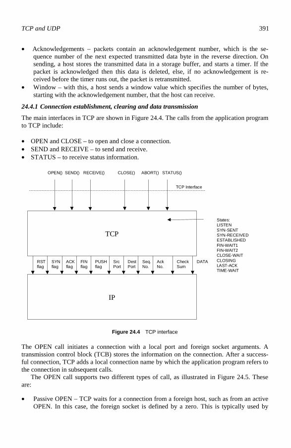
TCP and UDP 391
• Acknowledgements – packets contain an acknowledgement number, which is the se-quence number of the next expected transmitted data byte in the reverse direction. On sending, a host stores the transmitted data in a storage buffer, and starts a timer. If the packet is acknowledged then this data is deleted, else, if no acknowledgement is re-ceived before the timer runs out, the packet is retransmitted.
• Window – with this, a host sends a window value which specifies the number of bytes, starting with the acknowledgement number, that the host can receive.
24.4.1 Connection establishment, clearing and data transmission
The main interfaces in TCP are shown in Figure 24.4. The calls from the application program to TCP include: • OPEN and CLOSE – to open and close a connection. • SEND and RECEIVE – to send and receive. • STATUS – to receive status information.
TCP
IP
OPEN() SEND() RECEIVE() CLOSE() ABORT() STATUS()
States:LISTENSYN-SENTSYN-RECEIVEDESTABLISHEDFIN-WAIT1FIN-WAIT2CLOSE-WAITCLOSINGLAST-ACKTIME-WAIT
TCP Interface
RSTflag
SYNflag
SrcPort
DestPort
Seq.No.
AckNo.
ACKflag
FINflag
CheckSum
DATAPUSHflag
Figure 24.4 TCP interface
The OPEN call initiates a connection with a local port and foreign socket arguments. A transmission control block (TCB) stores the information on the connection. After a success-ful connection, TCP adds a local connection name by which the application program refers to the connection in subsequent calls. The OPEN call supports two different types of call, as illustrated in Figure 24.5. These are: • Passive OPEN – TCP waits for a connection from a foreign host, such as from an active
OPEN. In this case, the foreign socket is defined by a zero. This is typically used by

392 Computer busses
servers, such as TELNET and FTP servers. The connection can either be from a fully specified or an unspecified socket.
• Active OPEN – TCP actively connects to a foreign host, typically a server (which is opened with a passive OPEN). Two processes which issue active OPENs to each other, at the same time, will also be connected.
A connection is established with the transmission of TCP packets with the SYN control flag set and uses a three-way handshake (see Section 24.6). A connection is cleared by the ex-change of packets with the FIN control flag set. Data flows in a stream using the SEND call to send data and RECEIVE to receive data. The PUSH flag is used to send data in the SEND immediately to the recipient. This is required as a sending TCP is allowed to collect data from the sending application program and sends the data in segments when convenient. Thus, the PUSH flag forces it to be sent. When the receiving TCP sees the PUSH flag, it does not wait for any more data from the sending TCP before passing the data to the receiving process.
OPEN (active) OPEN (passive)Fully specifiedthe foreign socket
OPEN (active) OPEN (passive)Unspecifiedthe foreign socket
OPEN (active) OPEN (active)
Figure 24.5 TCP connections
24.5 TCB parameters
Table 24.2 outlines the send and receive packet parameters, as well as the current segment parameter, which are stored in the TCB. Along with this, the local and remote port number require to be stored.
24.6 Connection states
Figure 24.6 outlines the states the connection goes into, and the events that cause them. The events from applications programs are OPEN, SEND, RECEIVE, CLOSE, ABORT and STATUS, and the events from the incoming TCP packets include the SYN, ACK, RST and FIN flags. The definition of each of the connection states are:

TCP and UDP 393
Table 24.2 TCB parameters
Send sequence variables Receive sequence variables Current packet variable SND.UNA SND.NXT Send next
SND.WND Send window
SND.UP Send urgent pointer
SND.WL1 Segment sequence number used for last window update
SND.WL2 Segment acknowl-edgement number used for last window update
ISS Initial send sequence num-ber
RCV.NXT Receive next
RCV.WND Receive window
RCV.UP Receive urgent pointer
IRS Initial receive sequence number
SEG.SEQ Segment sequence number
SEG.ACK Segment acknowledgement number
SEG.LEN Segment length
SEG.WND Segment window
SEG.UP Segment urgent pointer
SEG.PRC Segment precedence value
• LISTEN – this is the state in which TCP is waiting for a remote connection on a given
port. • SYN-SENT– this is the state where TCP is waiting for a matching connection request
after it has sent a connection request. • SYN-RECEIVED – is the state where TCP is waiting for a confirming connection re-
quest acknowledgement after having both received and sent a connection request. • ESTABLISHED – this is the state that represents an open connection. Any data received
can be delivered to the application program. This is the normal state for data to be trans-mitted.
• FIN-WAIT-1– this is the state in which TCP is waiting for a connection termination re-quest, or an acknowledgement of a connection termination, from the remote TCP.
• FIN-WAIT-2 – this is the state in which TCP is waiting for a connection termination re-quest from the remote TCP.
• CLOSE-WAIT – this is the state where TCP is waiting for a connection termination re-quest from the local application.
• CLOSING – this is the state where TCP is waiting for a connection termination request acknowledgement from the remote TCP.
• LAST-ACK – this is the state where TCP is waiting for an acknowledgement of the con-nection termination request previously sent to the remote TCP.
• TIME-WAIT – this is the state in which TCP is waiting for enough time to pass to be sure the remote TCP received the acknowledgement of its connection termination re-quest.
• CLOSED – this is the notational state, which occurs after the connection has been closed.

394 Computer busses
CLOSECLOSE
LISTENLISTEN
ESTABLISHESTABLISHFINWAIT-1FIN
WAIT-1CLOSEWAIT
CLOSEWAIT
CLOSINGCLOSINGFIN WAIT-2FIN
WAIT-2 LAST-ACKLAST-ACK
SYN RECEIVED
SYN RECEIVED
SYN SENTSYN SENT
PassiveOPEN CLOSE
SEND andSYN
Receive SYNand SYN, ACK
Receive SYNand SYN, ACK
Receive ACKof SYN
ActiveOPEN CLOSE
CLOSE andFIN
Receive FINand ACK
Receive ACKof FIN
CLOSE andFIN
Receive FINand ACK
TIME WAITTIME WAIT
Receive ACKof FIN
CLOSEDCLOSED
CLOSE andFIN
Receive FINand ACK
Timeout = 2MSL
Figure 24.6 TCP connection states
24.6.1 Sequence numbers
TCP packets contain a 32-bit sequence number (0 to 4 294 967 295), which relates to every byte sent. It uses a cumulative acknowledgement scheme, where an acknowledgement with a value of VAL, validates all bytes up to, but not including, byte VAL. Each byte at which the packet starts is numbered consecutively, at the first byte. When sending data, TCP should receive acknowledgements for the transmitted data. The required TCB parameters will be:
SND.UNA Oldest unacknowledged sequence number. SND.NXT Next sequence number to send. SEG.ACK Acknowledgement from the receiving TCP (next sequence num-
ber expected by the receiving TCP). SEG.SEQ First sequence number of a segment. SEG.LEN Number of bytes in the TCP packet. SEG.SEQ+SEG.LEN–1 Last sequence number of a segment.
On receiving data, the following TCB parameters are required:
RCV.NXT Next sequence number expected on an incoming segment, and is the left or lower edge of the receive window.
RCV.NXT+RCV.WND–1 Last sequence number expected on an incoming segment, and is

TCP and UDP 395
the right or upper edge of the receive window. SEG.SEQ First sequence number occupied by the incoming segment. SEG.SEQ+SEG.LEN–1 Last sequence number occupied by the incoming segment.
24.6.2 ISN selection
The initial sequence number (ISN) is selected so that previous sockets are not confused with new sockets. Typically, this can happen when a host application crashes and then quickly re-establishes the connection before the other side can time-out the connection. To avoid this a 32-bit initial sequence number (ISN) generator is created when the connection is made. The number is generated by a 32-bit clock, which is incremented approximately every 4µs (giv-ing an ISN cycle of 4.55 hours). Thus, within 4.55 hours, each ISN will be unique. As each connection has a send and receive sequence number, these are an initial send sequence number (ISS) and an initial receive sequence number (IRS). When establishing a connection, the two TCPs synchronise their initial sequence numbers. This is done by ex-changing connection establishing packets, with the SYN bit set and with the initial sequence numbers (these packets are typically called SYNs). Thus four packets must be initially ex-changed: • A sends to B. SYN with ASEQ. • B sends to A. ACK of the sequence number (ASEQ). • B sends to A. SYN with BSEQ. • A sends to B. ACK of the sequence number (BSEQ). Note that the two intermediate steps can be combined into a single message. This is some-times knows as a three-way handshake. This handshake is necessary as the sequence num-bers are not tied to a global clock, only to local clocks, and has many advantages, including the fact that old packets will be discarded as they occurred in a previous time. To make sure that a sequence number is not duplicated, a host must wait for a maximum segment lifetime (MSL) before starting to retransmit packets (segments) after start-up or when recovering from a crash. An example MSL is 2 minutes. However, if it is recovering, and it has a memory of the previous sequence numbers, it may not need to wait for the MSL, as it can use sequence numbers which are much greater than the previously used sequence numbers.
24.7 Opening and closing a connection
Figure 24.7 shows a basic three-way handshake. The steps are: 1. The initial state on the initiator is CLOSED and, on the recipient, it is LISTEN (the re-
cipient is waiting for a connection see figure 24.7). 2. The initiator goes into the SYN-SENT state and sends a packet with the SYN bit set and
then indicates that the starting sequence number will be 999 (the current sequence num-ber, thus the next number sent will be 1000). When this is received the recipient goes into the SYN-RECEIVED state.
3. The recipient sends back a TCP packet with the SYN and ACK bits set (which identifies that it is a SYN packet and also that it is acknowledging the previous SYN packet). In

396 Computer busses
this case, the recipient tells the originator that it will start transmitting at a sequence number of 100. The acknowledgement number is 1000, which is the sequence number that the recipient expects to receive next. When this is received, the originator goes into the ESTABLISHED state.
4. The originator sends back a TCP packet with the SYN and ACK bits set and the ac-knowledgement number is 101, which is the sequence number it expects to see next.
5. The originator transmits data with the sequence number of 1000. Originator Recipient 1. CLOSED LISTEN 2. SYN-SENT → <SEQ=999><CTL=SYN> SYN-RECEIVED 3. ESTABLISHED <SEQ=100><ACK=1000> <CTL=SYN,ACK> ← SYN-RECEIVED 4. ESTABLISHED → <SEQ=1000><ACK=101> <CTL=ACK> ESTABLISHED 5. ESTABLISHED → <SEQ=1000><ACK=101> <CTL=ACK><DATA> ESTABLISHED
Figure 24.7 TCP connection
Note that the acknowledgement number acknowledges every sequence number up to but not including the acknowledgement number. Figure 24.8 shows how the three-way handshake prevents old duplicate connection initia-tions from causing confusion. In state 3, a duplicate SYN has been received, which is from a previous connection. The recipient sends back an acknowledgement for this (4), but when this is received by the originator, the originator sends back a RST (reset) packet. This causes the recipient to go back into a LISTEN state. It will then receive the SYN packet sent in 2, and after acknowledging it, a connection is made. TCP connections are half-open if one of the TCPs has closed or aborted, and the other end is still connected. They can also occur if the two connections have become desynchro-nised because of a system crash. This connection is automatically reset if data is sent in ei-ther direction. This is because the sequence numbers will be incorrect, otherwise the connec-tion will time-out. A connection is normally closed with the CLOSE call. A host who has closed cannot continue to send, but can continue to RECEIVE until it is told to close by the other side. Fig-ure 24.9 shows a typical sequence for closing a connection. Normally the application pro-gram sends a CLOSE call for the given connection. Next, a TCP packet is sent with the FIN bit set, the originator enters into the FIN-WAIT-1 state. When the other TCP has acknowl-edged the FIN and sent a FIN of its own, the first TCP can ACK this FIN. Originator Recipient 1. CLOSED LISTEN 2. SYN-SENT → <SEQ=999><CTL=SYN> 3. (duplicate) → <SEQ=900><CTL=SYN> 4. SYN-SENT <SEQ=100><ACK=901> <CTL=SYN,ACK> ← SYN-RECEIVED 5. SYN-SENT → <SEQ=901><CTL=RST> LISTEN 6. (packet 2 received) → 7. SYN-SENT <SEQ=100><ACK=1000><CTL=SYN,ACK> ← SYN-RECEIVED 8. ESTABLISHED → <SEQ=1000><ACK=101><CTL=ACK><DATA> ESTABLISHED
Figure 24.8 TCP connection with duplicate connections

TCP and UDP 397
Originator Recipient 1. ESTABLISHED ESTABLISHED (CLOSE call) 2. FIN-WAIT-1 → <SEQ=1000><ACK=99> <CTL=SFIN,ACK> CLOSE-WAIT 3. FIN-WAIT-2 <SEQ=99><ACK=1001> <CTL=ACK> ← CLOSE-WAIT 4. TIME-WAIT <SEQ=99><ACK=101><CTL=FIN,ACK> ← LAST-ACK 5. TIME-WAIT → <SEQ=1001><ACK=102><CTL=ACK> CLOSED
Figure 24.9 TCP close connection
24.8 TCP user commands
The commands in this section characterise the interface between TCP and the application program. Their actual implementation depends on the operating system. Section 24.9 dis-cusses the WinSock implementation.
24.8.1 OPEN
The OPEN call initiates an active or a passive TCP connection. The basic parameters passed and returned from the call are given next. Parameters in brackets are optional.
Parameters passed: local port, foreign socket, active/passive [, timeout] [, precedence] [, security/compartment] [, options]) Parameters returned: local connection name
These parameters are defined as: • Local port – the local port to be used. • Foreign socket – the definition of the foreign socket. • Active/passive – a passive flag causes TCP to LISTEN, else it will actively seek a con-
nection. • Timeout – if present, this parameter allows the caller to set up a timeout for all data sub-
mitted to TCP. If the data is not transmitted successfully within the timeout period, the connection is aborted.
• Security/compartment – specifies the security of the connection. • Local connection name – a unique connection name is returned which identifies the
socket.
24.8.2 SEND
The SEND call causes the data in the output buffer to be sent to the indicated connection. Most implementations return immediately from the SEND call, even if the data has not been sent, although some implementations will not return until either there is a timeout or the data has been sent. The basic parameters passed and returned from the call are given next. Pa-rameters in brackets are optional.
Parameters passed: local connection name, buffer address, byte count, PUSH flag, URGENT flag [,timeout]

398 Computer busses
These parameters are defined as: • Local connection name – a unique connection name which identifies the socket. • Buffer address – address of data buffer. • Byte count – number of bytes in the buffer. • PUSH flag – if this flag is set then the data will be transmitted immediately, else the TCP
may wait until it has enough data. • URGENT flag – sets the urgent pointer. • Timeout – sets a new timeout for the connection.
24.8.3 RECEIVE
The RECEIVE call allocates a receiving buffer for the specified connection. Most implemen-tations return immediately from the RECEIVE call, even if the data has not been received, although some implementation will not return until either there is a timeout or the data has been received. The basic parameters passed and returned from the call are given next. Pa-rameters in brackets are optional.
Parameters passed: local connection name, buffer address, byte count Parameters returned: byte count, URGENT flag, PUSH flag
These parameters are defined as: • Local connection name – a unique connection name which identifies the socket. • Buffer address – address of the receive data buffer. • Byte count – number of bytes received in the buffer. • PUSH flag – if this flag is set then the PUSH flag has been set on the received data. • URGENT flag – if this flag is set then the URGENT flag has been set on the received
data.
24.8.4 CLOSE
The CLOSE call closes the connections and releases associated resources. All pending SENDs will be transmitted, but after the CLOSE call has been implemented, no further SENDs can occur. RECEIVEs can occur until the other host has also closed the connection. The basic parameters passed and returned from the call are given next.
Parameters passed: local connection name
24.8.5 STATUS
The STATUS call determines the current status of a connection, typically listing the TCBs. The basic parameters passed and returned from the call are given next.
Parameters passed: local connection name Parameters returned: status data
The returned information should include status information on the following: • local socket, foreign socket, local connection name;

TCP and UDP 399
• receive window, send window, connection state; • number of buffers awaiting acknowledgement, number of buffers pending receipt; • urgent state, precedence, security/compartment; • transmission timeout.
24.8.6 ABORT
The ABORT call causes all pending SENDs and RECEIVEs to be aborted. All TCBs are also removed and a RESET message sent to the other TCP. The basic parameters passed and returned from the call are given next. Parameters in brackets are optional. Parameters passed: local connection name
24.9 WinSock
24.9.1 Introduction
The Windows sockets specification describes a common interface for networked Windows programs. WinSock uses TCP/IP communications and provides for binary and source code compatibility for different network types. The Windows sockets API (WinSock application programming interface or WSA) is a library of functions that implement the socket interface by the Berkley Software distribution of UNIX. WinSock augments the Berkley socket implementation by adding Windows-specific extensions to support the message-driven nature of Windows system. The basic implementation normally involves: • Opening a socket – this allows for multiple connections with multiple hosts. Each socket
has a unique identifier. It normally involves defining the protocol suite, the socket type and the protocol name. The API call used for this is socket().
• Naming a socket – this involves assigning location and identity attributes to a socket. The API call used for this is bind().
• Associate with another socket – this involves either listening for a connection or actively seeking a connection. The API calls used in this are listen(), connect()and ac-cept().
• Send and receive between sockets – the API calls used in this are send(), sendto(), recv() and recvfrom().
• Close the socket – the API calls used in this are close() and shutdown().
24.9.2 Windows sockets
The main WinSock API calls are:
socket() Creates a socket. accept() Accepts a connection on a socket. connect() Establishes a connection to a peer. bind() Associates a local address with a socket. listen() Establishes a socket to listen for incoming connection.

400 Computer busses
send() Sends data on a connected socket. sendto() Sends data on an unconnected socket. recv() Receives data from a connected socket. recvfrom() Receives data from an unconnected socket. shutdown() Disables send or receive operations on a socket. closesocket() Closes a socket.
Figure 24.10 shows the operation of a connection of a client to a server. The server is defined as the computer which waits for a connection, the client is the computer which initially makes contact with the server. On the server the computer initially creates a socket with the socket() function, and this is bound to a name with the bind() function. After this, the server listens for a connection with the listen() function. When the client calls the connect() function the server then accepts the connection with accept(). After this the server and client can send and receive data with the send() or recv() functions. When the data transfer is complete the close-socket() is used to close the socket.
socket()create a socket
bind()give socket a
name
listen()listen for
connections
accept()accept a newconnection
send()/recv()send/receive
data
closesocket()close a socket
socket()create a socket
connect()connect to a socket
send()/recv()send/receive
data
closesocket()close a socket
Server Client
Figure 24.10 WinSock connection
socket()
The socket() function creates a socket. Its syntax is

TCP and UDP 401
SOCKET socket (int af, int type, int protocol)
where af A value of PF_INET specifies the ARPA Internet address format specifica-
tion (others include AF_IPX for SPX/IPX and AF_APPLETALK for Apple-Talk).
type Socket specification, which is typically either SOCK_STREAM or SOCK_DGRAM. The SOCK_STREAM uses TCP and provides a sequenced, reliable, two-way, connection-based stream. SOCK_DGRAM uses UDP and provides for connec-tionless datagrams. This type of connection is not recommended. A third type is SOCK_RAW, for types other than UDP or TCP, such as for ICMP.
protocol Defines the protocol to be used with the socket. If it is zero then the caller does not wish to specify a protocol.
If the socket function succeeds then the return value is a descriptor referencing the new socket. Otherwise, it returns SOCKET_ERROR, and the specific error code can be tested with WSAGetLastError. An example creation of a socket is given next: SOCKET s; s=socket(PF_INET,SOCK_STREAM,0); if (s == INVALID_SOCKET) cout << ″Socket error″
bind()
The bind() function associates a local address with a socket. It is called before the connect or listen function. When a socket is created with socket, it exists in a name space (address family), but it has no name assigned. The bind function gives the socket a local association (host address/port number). Its syntax is: int bind(SOCKET s, const struct sockaddr FAR * addr, int namelen) where s A descriptor identifying an unbound socket. namelen The length of addr. addr The address to assign to the socket. The sockaddr structure is defined as follows: struct sockaddr u_short sa_family; char sa_data[14]; ; In the Internet address family, the sockadd_in structure is used by Windows Sockets to spec-ify a local or remote endpoint address to which to connect a socket. This is the form of the sockaddr structure specific to the Internet address family and can be cast to sockaddr. This

402 Computer busses
structure can be filled with the sockaddr_in structure which has the following form:
struct SOCKADDR_IN short sin_family; unsigned short sin_port; struct in_addr sin_addr; char sin_zero[8];
where
sin_family must be set to AF_INET. sin_port IP port. sin_addr IP address. sin_zero padding to make structure the same size as sockaddr.
If an application does not care what address is assigned to it, it may specify an Internet ad-dress equal to INADDR_ANY, a port equal to 0, or both. An Internet address equal to INADDR_ANY causes any appropriate network interface be used. A port value of 0 causes the Windows sockets implementation to assign a unique port to the application with a value be-tween 1024 and 5000. If no error occurs then it returns a zero value. Otherwise, it returns INVALID_SOCKET, and the specific error code can be tested with WSAGetLastError. If an application needs to bind to an arbitrary port outside of the range 1024 to 5000 then the following outline code can be used:
#include <windows.h> #include <winsock.h> int main(void) SOCKADDR_IN sin;
SOCKET s; s = socket(AF_INET,SOCK_STREAM,0); if (s == INVALID_SOCKET) // Socket failed sin.sin_family = AF_INET; sin.sin_addr.s_addr = 0; sin.sin_port = htons(100); // port=100 if (bind(s, (LPSOCKADDR)&sin, sizeof (sin)) == 0) // Bind failed return(0); The Windows sockets htons function converts an unsigned short (u_short) from host byte order to network byte order.

TCP and UDP 403
connect()
The connect() function establishes a connection with a peer. If the specified socket is un-bound then unique values are assigned to the local association by the system and the socket is marked as bound. Its syntax is
int connect (SOCKET s, const struct sockaddr FAR * name, int namelen)
where
s Descriptor identifying an unconnected socket. name Name of the peer to which the socket is to be connected. namelen Name length.
If no error occurs then it returns a zero value. Otherwise, it returns SOCKET_ERROR, and the specific error code can be tested with WSAGetLastError.
listen()
The listen() function establishes a socket which listens for an incoming connection. The sequence to create and accept a socket is: • socket()– Creates a socket. • listen()– this creates a queue for incoming connections and is typically used by a
server that can have more than one connection at a time. • accept()– these connections are then accepted with accept. The syntax of listen() is
int listen (SOCKET s, int backlog) where
s Describes a bound, unconnected socket. backlog Defines the queue size for the maximum number of pending connections
may grow (typically a maximum of 5).
If no error occurs then it returns a zero value. Otherwise, it returns SOCKET_ERROR, and the specific error code can be tested with WSAGetLastError. #include <windows.h> #include <winsock.h> int main(void) SOCKADDR_IN sin; SOCKET s; s = socket(AF_INET,SOCK_STREAM,0); if (s == INVALID_SOCKET)

404 Computer busses
// Socket failed sin.sin_family = AF_INET; sin.sin_addr.s_addr = 0; sin.sin_port = htons(100); // port=100 if (bind(s, (struct sockaddr FAR *)&sin, sizeof (sin))==SOCKET_ERROR) // Bind failed if (listen(s,4)==SOCKET_ERROR) // Listen failed return(0);
accept()
The accept() function accepts a connection on a socket. It extracts any pending connections from the queue and creates a new socket with the same properties as the specified socket. Finally, it returns a handle to the new socket. Its syntax is
SOCKET accept(SOCKET s, struct sockaddr FAR *addr, int FAR *addrlen )
where
s Descriptor identifying a socket that is in listen mode. addr Pointer to a buffer that receives the address of the connecting entity, as
known to the communications layer. addrlen Pointer to an integer which contains the length of the address addr.
If no error occurs then it returns a zero value. Otherwise, it returns INVALID_SOCKET, and the specific error code can be tested with WSAGetLastError. #include <windows.h> #include <winsock.h> int main(void) SOCKADDR_IN sin; SOCKET s; int sin_len; s = socket(AF_INET,SOCK_STREAM,0); if (s == INVALID_SOCKET) // Socket failed sin.sin_family = AF_INET; sin.sin_addr.s_addr = 0; sin.sin_port = htons(100); // port=100

TCP and UDP 405
if (bind(s, (struct sockaddr FAR *)&sin, sizeof (sin))==SOCKET_ERROR) // Bind failed if (listen(s,4)<0) // Listen failed sin_len = sizeof(sin); s=accept(s,(struct sockaddr FAR *) & sin,(int FAR *) &sin_len); if (s==INVALID_SOCKET) // Accept failed return(0);
send()
The send() function sends data to a connected socket. Its syntax is:
int send (SOCKET s, const char FAR *buf, int len, int flags)
where
s Connected socket descriptor. buf Transmission data buffer. len Buffer length. flags Calling flag.
The flags parameter influences the behaviour of the function. These can be
MSG_DONTROUTE Specifies that the data should not be subject to routing. MSG_OOB Send out-of-band data.
If send() succeeds then the return value is the number of characters sent (which can be less than the number indicated by len). Otherwise, it returns SOCKET_ERROR, and the specific error code can be tested with WSAGetLastError. #include <windows.h> #include <winsock.h> #include <string.h> #define STRLENGTH 100 int main(void) SOCKADDR_IN sin; SOCKET s; int sin_len; char sendbuf[STRLENGTH]; s = socket(AF_INET,SOCK_STREAM,0); if (s == INVALID_SOCKET)

406 Computer busses
// Socket failed sin.sin_family = AF_INET; sin.sin_addr.s_addr = 0; sin.sin_port = htons(100); // port=100 if (bind(s, (struct sockaddr FAR *)&sin, sizeof (sin))==SOCKET_ERROR) // Bind failed if (listen(s,4)<0) // Listen failed sin_len = sizeof(sin); s=accept(s,(struct sockaddr FAR *) & sin,(int FAR *) &sin_len); if (s<0) // Accept failed while (1) // get message to send and put into sendbuff send(s,sendbuf,strlen(sendbuf),80); return(0);
recv()
The recv() function receives data from a socket. It waits until data arrives and its syntax is:
int recv(SOCKET s, char FAR *buf, int len, int flags)
where
s Connected socket descriptor. buf Incoming data buffer. len Buffer length. flags Specifies the method by which the data is received.
If recv() succeeds then the return value is the number of bytes received (a zero identifies that the connection has been closed). Otherwise, it returns SOCKET_ERROR, and the specific error code can be tested with WSAGetLastError. The flags parameter may have one of the following values:
MSG_PEEK Peek at the incoming data. Any received data is copied into the buffer, but not removed from the input queue.
MSG_OOB Process out-of-band data. #include <windows.h> #include <winsock.h>

TCP and UDP 407
#define STRLENGTH 100 int main(void) SOCKADDR_IN sin; SOCKET s; int sin_len,status; char recmsg[STRLENGTH]; s = socket(AF_INET,SOCK_STREAM,0); if (s == INVALID_SOCKET) // Socket failed sin.sin_family = AF_INET; sin.sin_addr.s_addr = 0; sin.sin_port = htons(100); // port=100 if (bind(s, (struct sockaddr FAR *)&sin, sizeof (sin))==SOCKET_ERROR) // Bind failed if (listen(s,4)<0) // Listen failed sin_len = sizeof(sin); s=accept(s,(struct sockaddr FAR *) & sin,(int FAR *) &sin_len); if (s<0) // Accept failed while (1) status=recv(s,recmsg,STRLENGTH,80); if (status==SOCKET_ERROR) // no socket break; recmsg[status]=NULL; // terminate string if (status) // szMsg contains received string else break; // connection broken return(0);

408 Computer busses
shutdown()
The shutdown() function disables send or receive operations on a socket and does not close any opened sockets. Its syntax is
int shutdown(SOCKET s, int how)
where
s Socket descriptor. how Flag that identifies operation types that will no longer be allowed. These are:
0 – Disallows subsequent receives. 1 – Disallows subsequent sends. 2 – Disables send and receive. If no error occurs then it returns a zero value. Otherwise, it returns INVALID_SOCKET, and the specific error code can be tested with WSAGetLastError.
closesocket()
The closesocket() function closes a socket. Its syntax is:
int closesocket (SOCKET s);
where
s Socket descriptor. If no error occurs then it returns a zero value. Otherwise, it returns INVALID_SOCKET, and the specific error code can be tested with WSAGetLastError.
24.10 Visual Basic socket implementation
Visual Basic supports a WinSock control and allows the connection of hosts over a network. It supports both UDP and TCP. Figure 24.11 shows a sample Visual Basic screen with a WinSock object (in this case, it is named Winsock1). To set the protocol used then either select the properties window on the WinSock object, click protocol and select sckTCPProto-col, or sckUDPProtocol. Otherwise, within the code it can be set to TCP with: Winsock1.Protocol = sckTCPProtocol The WinSock object has various properties, such as:
obj.RemoteHost Defines the IP address or domain name of the remote host. obj.LocalPort Defines the local port number.
The methods that are used with the WinSock object are:

TCP and UDP 409
obj.Connect Connects to a remote host (client invoked). obj.Listen Listens for a connection (server invoked). obj.GetData Reads data from the input steam. obj.SendData Sends data to an output stream.
The main events are:
ConnectionRequest Occurs when a remote host wants to make a connection with a server.
DataArrival Occurs when data has arrived from a connection (data is then read with GetData).
Figure 24.11 WinSock object
24.10.1 Creating a server
A server must listen for connection. To do this, do the following: 1 Create a new standard EXE project. 2 Change the name of the default form to myServer. 3 Change the caption of the form to ‘Server Application’ (see Figure 24.12). 4 Put a WinSock control on the main form and change its name to myTCPServer. 5 Add two TextBox controls to the form. Name the first SendTextData, and the second
ShowText (see Figure 24.12).
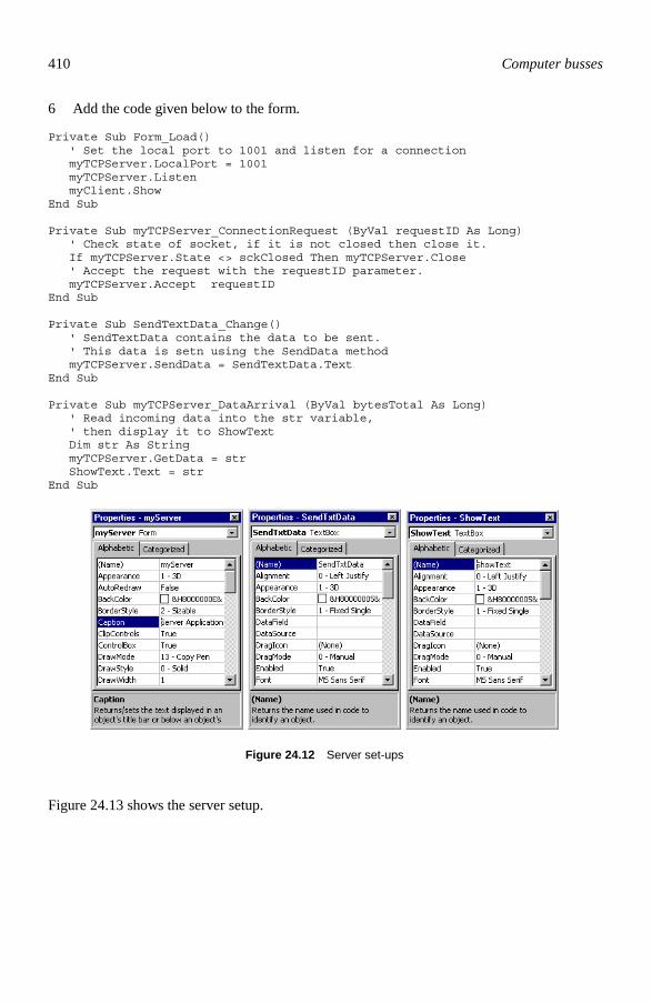
410 Computer busses
6 Add the code given below to the form. Private Sub Form_Load() ' Set the local port to 1001 and listen for a connection myTCPServer.LocalPort = 1001 myTCPServer.Listen myClient.Show End Sub Private Sub myTCPServer_ConnectionRequest (ByVal requestID As Long) ' Check state of socket, if it is not closed then close it. If myTCPServer.State <> sckClosed Then myTCPServer.Close ' Accept the request with the requestID parameter. myTCPServer.Accept requestID End Sub Private Sub SendTextData_Change() ' SendTextData contains the data to be sent. ' This data is setn using the SendData method myTCPServer.SendData = SendTextData.Text End Sub Private Sub myTCPServer_DataArrival (ByVal bytesTotal As Long) ' Read incoming data into the str variable, ' then display it to ShowText Dim str As String myTCPServer.GetData = str ShowText.Text = str End Sub
Figure 24.12 Server set-ups
Figure 24.13 shows the server setup.

TCP and UDP 411
Figure 24.13 Server form
24.10.2 Creating a client
The client must actively seek a connection. To create a client, do the following: 1 Add a new form to the project, and name it myClient. 2 Change the caption of the form to ‘Client Application’. 3 Add a WinSock control to the form and name it myTCPClient. 4 Add two TextBox controls to the form. Name the first SendTextData, and the second
ShowText. 5 Draw a CommandButton control on the form and name it cmdConnect. 6 Change the caption of the CommandButton control to Connect. 7 Add the code given below to the form.
Private Sub Form_Load() ' In this case it will connect to 146.176.151.130 ' change this to the local IP address or DNS of the local computer myTCPClient.RemoteHost = "146.176.151.130" myTCPClient.RemotePort = 1001 End Sub Private Sub cmdConnect_Click() ' Connect to the server myTCPClient.Connect End Sub Private Sub SendTextData_Change() tcpClient.SendData txtSend.Text

412 Computer busses
End Sub Private Sub tcpClient_DataArrival (ByVal bytesTotal As Long) Dim str As String myTCPClient.GetData str ShowText.Text = str End Sub
Figure 24.14 Client form
The program, when it is run, will act as a client and a server. Any text typed in the SendTxtData TextBox will be sent to the ShowText TextBox on the other form.
24.10.3 Multiple connections
In Visual Basic, it is also possible to create multiple connections to a server. This is done by creating multiple occurrences of the server object. A new one is created every time there is a new connection (with the Connection_Request event). Each new server accepts the incoming connection. The following code, which has a WinSock control on a form called multServer, is given below.
Private ConnectNo As Long Private Sub Form_Load() ConnectNo = 0 multServer(0).LocalPort = 1001 multServer(0).Listen End Sub Private Sub multServer_ConnectionRequest _

TCP and UDP 413
(Index As Integer, ByVal requestID As Long) If Index = 0 Then ConnectNo = ConnectNo + 1 Load multServer(ConnectNo) multServer(ConnectNo).LocalPort = 0 multServer(ConnectNo).Accept requestID Load txtData(ConnectNo) End If End Sub
24.10.4 Connect event
The Connect event connects to a server. If an error occurs then a flag (ErrorOccurred) is set to True, else it is False. Its syntax is
Private Sub object.Connect(ErrorOccurred As Boolean)
24.10.5 Close event
The Close event occurs when the remote computer closes the connection. Applications should use the Close method to correctly close their connection. Its syntax is
object_Close()
24.10.6 DataArrival event
The DataArrival event occurs when new data arrives, and returns the number of bytes read (bytesTotal). Its syntax is
object_DataArrival (bytesTotal As Long)
24.10.7 Bind method
The Bind method specifies the local port (LocalPort) and the local IP address (LocalIP) to be used for TCP connections. Its syntax is
object.Bind LocalPort, LocalIP
24.10.8 Listen method
The Listen method creates a socket and goes into listen mode (for server applications). Its stays in this mode until a ConnectionRequest event occurs, which indicates an incoming con-nection. After this, the Accept method should be used to accept the connection. Its syntax is:
object.Listen
24.10.9 Accept method
The Accept method accepts incoming connections after a ConnectionRequest event. Its syn-tax is
object.Accept requestID The requestID parameter is passed into the ConnectionRequest event and is used with the

414 Computer busses
Accept method.
24.10.10 Close method
The Close method closes a TCP connection. Its syntax is
object.Close
24.10.11 SendData method
The SendData methods sends data (Data) to a remote computer. Its syntax is
object.SendData Data
24.10.12 GetData method
The GetData method gets data (Data) from an object. Its syntax is
object.GetData data, [type,] [maxLen]
24.11 Exercises
24.11.1 Which of the following is not part of a TCP header: (a) Host IP address (b) Time-to-live field (c) Host port number (d) Acknowledgement number 24.11.2 Which port does a TELNET server listen to: (a) 21 (b) 25 (c) 25 (d) 80 24.11.3 Which port does an Email server (using SMTP) listen to: (a) 21 (b) 25 (c) 25 (d) 80 24.11.4 Which port does a WWW server (using HTTP) listen to: (a) 21 (b) 25 (c) 25 (d) 80 24.11.5 Which port does an FTP server listen to: (a) 21 (b) 25 (c) 25 (d) 80 24.11.6 What is the main difference between UDP and TCP: (a) TCP uses sequence numbers, makes connections and uses acknowledge-

TCP and UDP 415
ments. (b) They use different addressing schemes. (c) They use different port allocations. (d) UDP only supports one-way traffic, while TCP supports multiplexed traf-
fic. 24.11.7 What is the main method that TCP uses to create a reliable connection: (a) Enhanced error correction (b) Specially coded data (c) Encrypted data (d) Sequence numbers and acknowledgements 24.11.8 How is the initial sequence number of a TCP packet generated: (a) Randomly (b) From a 32-bit clock which is updated every 4 µs (c) From a universal Internet-based clock (d) From the system clock 24.11.9 How many packets are exchanged in setting up an established TCP connection: (a) 1 (b) 2 (c) 3 (d) 4 24.11.10 Outline the operation of the three-way handshaking. 24.11.11 What advantages does TCP have over UDP. Investigate server applications which
use UDP. 24.11.12 If possible, implement a basic client/server application with either C++ or Visual
Basic. As a test, run the client and the server on the same computer. (Note the IP address of the computer as this is required by the client.)
24.11.13 Change the program in Exercise 24.11.12 so that the client and the server run on
different computers (note the IP address of the server as this is required by the cli-ent). If possible, run the program on different network segments.
For the following questions, download a program from the WWW which connects
to a specified port on a specified server. 24.11.14 Connect to a WWW server using port 13. This port should return the current date
and time. 24.11.15 Connect to a WWW server using port 19. 24.11.16 Connect two computers over a network and set up a chat connection. One of the
computers should be the chat server and the other the chat client. Modify it so that the server accepts calls from one or many clients.

416 Computer busses
24.12 TCP/IP services reference
Port Service Comment Port Service Comment 1 TCPmux 7 echo 9 discard Null 11 systat Users 13 daytime 15 netstat 17 qotd Quote 18 msp Message send protocol 19 chargen ttytst source 21 ftp 23 telnet 25 smtp Mail 37 time Timserver 39 rlp Resource location 42 nameserver IEN 116 43 whois Nicname 53 domain DNS 57 mtp Deprecated 67 bootps BOOTP server 67 bootps 68 bootpc BOOTP client 69 tftp 70 gopher Internet Gopher 77 rje Netrjs 79 finger 80 www WWW HTTP 87 link Ttylink 88 kerberos Kerberos v5 95 supdup 101 hostnames 102 iso-tsap ISODE 105 csnet-ns CSO name server 107 rtelnet Remote Telnet 109 pop2 POP version 2 110 pop3 POP version 3 111 sunrpc 113 auth Rap ID 115 sftp 117 uucp-path 119 nntp USENET 123 ntp Network Timel 137 netbios-ns NETBIOS name service 138 netbios-dgm NETBIOS 139 netbios-ssn NETBIOS session 143 imap2 161 snmp SNMP 162 snmp-trap SNMP trap 163 cmip-man ISO management over IP 164 cmip-agent 177 xdmcp X display manager 178 nextstep NeXTStep 179 bgp BGP 191 prospero 194 irc Internet relay chat 199 smux SNMP multiplexor 201 at-rtmp AppleTalk routing 202 at-nbp AppleTalk name binding 204 at-echo AppleTalk echo 206 at-zis AppleTalk zone information 210 z3950 NISO Z39.50 database 213 ipx IPX 220 imap3 Interactive mail access 372 ulistserv UNIX Listserv 512 exec Comsat 513 login 513 who Whod 514 shell No passwords used 514 syslog 515 printer Line printer spooler 517 talk 518 ntalk 520 route RIP 525 timed Timeserver 526 tempo Newdate 530 courier Rpc 531 conference Chat 532 netnews Readnews 533 netwall Emergency broadcasts 540 uucp Uucp daemon 543 klogin Kerberized ‘rlogin’ (v5) 544 kshell Kerberized ‘rsh’ (v5)
24.13 Notes from the author
In this chapter I have presented the two opposite ends of code development for TCP/IP com-munications. The C++ code is complex, but very powerful, and allows for a great deal of flexibility. On the other hand, the Visual Basic code is simple to implement but is difficult to

TCP and UDP 417
implement for non-typical applications. Thus, the code used tends to reflect the type of appli-cation. In many cases Visual Basic gives an easy-to-implement package, with the required functionality. I’ve seen many a student wilt at the prospect of implementing a Microsoft Win-dows program in C++. ‘Where do I start’, is always the first comment, and then ‘How do I do text input’, and so on. Visual Basic, on the other hand, has matured into an excellent de-velopment system which hides much of the complexity of Microsoft Windows away from the developer. So, don’t worry about computer language snobbery. Pick the best language to implement the specification. UDP transmission can be likened to sending electronic mail. In most electronic mail packages the user can request that a receipt is sent back to the originator when the elec-tronic mail has been opened. This is equivalent to TCP, where data is acknowledged after a certain amount of data has been sent. If the user does not receive a receipt for their elec-tronic mail then they will send another one, until it is receipted or until there is a reply. UDP is equivalent to a user sending an electronic mail without asking for a receipt, thus the origi-nator has no idea if the data has been received, or not. TCP/IP is an excellent method for networked communications, as IP provides the routing of the data, and TCP allows acknowledgements for the data. Thus, the data can always be guaranteed to be correct. Unfortunately there is an overhead in the connection of the TCP socket, where the two communicating stations must exchange parameters before the connec-tion is made, then they must maintain and acknowledge received TCP packets. UDP has the advantage that it is connectionless. So there is no need for a connection to be made, and data is simply thrown in the network, without the requirement for acknowledgments. Thus UDP packets are much less reliable in their operation, and a sending station cannot guarantee that the data is going to be received. UDP is thus useful for remote data acquisition where data can be simply transmitted without it being requested or without a TCP/IP connection being made. The concept of ports and sockets is important in TCP/IP. Servers wait and listen on a given port number. They only read packets which have the correct port number. For exam-ple, a WWW server listens for data on port 80, and an FTP server listens for port 21. Thus a properly set up communication network requires a knowledge of the ports which are ac-cessed. An excellent method for virus writers and hackers to get into a network is to install a program which responds to a given port which the hacker uses to connect to. Once into the system they can do a great deal of damage. Programming languages such as Java have built-in security to reduce this problem.
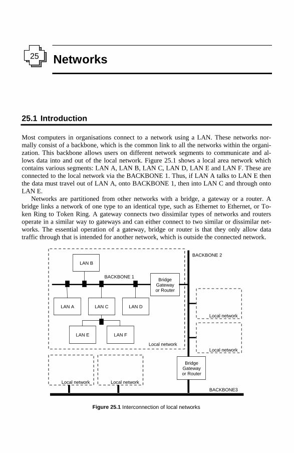
Networks
25.1 Introduction
Most computers in organisations connect to a network using a LAN. These networks nor-mally consist of a backbone, which is the common link to all the networks within the organi-zation. This backbone allows users on different network segments to communicate and al-lows data into and out of the local network. Figure 25.1 shows a local area network which contains various segments: LAN A, LAN B, LAN C, LAN D, LAN E and LAN F. These are connected to the local network via the BACKBONE 1. Thus, if LAN A talks to LAN E then the data must travel out of LAN A, onto BACKBONE 1, then into LAN C and through onto LAN E. Networks are partitioned from other networks with a bridge, a gateway or a router. A bridge links a network of one type to an identical type, such as Ethernet to Ethernet, or To-ken Ring to Token Ring. A gateway connects two dissimilar types of networks and routers operate in a similar way to gateways and can either connect to two similar or dissimilar net-works. The essential operation of a gateway, bridge or router is that they only allow data traffic through that is intended for another network, which is outside the connected network.
LAN A LAN C LAN D
LAN E
LAN B
Bridge Gateway or Router
LAN F
BACKBONE 1
BACKBONE 2
Local network
Local network
Local network
Local network Local network BACKBONE3
Bridge Gateway or Router
Figure 25.1 Interconnection of local networks
25

420 Computer busses
This filters traffic and stops traffic, not intended for the network, from clogging-up the back-bone. Most modern bridges, gateways and routers are intelligent and can automatically de-termine the topology of the network. Spanning-tree bridges have built-in intelligence and can communicate with other bridges. They can then build up a picture of the interconnected networks. So, if more than one path exists between individual segments, the bridge automatically finds alternate routes. This is useful when a fault develops on a route or a route becomes too heavily loaded. Conventional bridges can cause frames to loop around forever.
25.1.1 Peer-to-peer and client/server
An important concept is the differentiation between a peer-to-peer connection and a cli-ent/server connection. A peer-to-peer connection allows users on a local network access to a local computer. Typically, this might be access to:
Local printers – Printers, local to a computer, can be accessed by other users if the printer is shareable. This can be password protected, or not. Shareable printers on a Microsoft network have a small hand under the icon.
Local disk drives and folders – The disk drives, such as the hard disk or CD-ROM drives can be accessed if they are shareable. Normally the drives must be shareable. On a Microsoft network a drive can be made shareable by select-ing the drive and selecting the right-hand mouse button, then selecting the Sharing option. User names and passwords can be set-up locally or can be accessed from a network server. Typically, only the local computer grants access to certain folders, whereas others are not shared.
These shared resources can also be mounted as disk drives to the remote computer. Thus, the user of the remote computer can simply access resources on the other computers as if they were mounted locally. This option is often the best when there is a small local network, as it requires the minimum of set-up and does not need any complicated server set-ups. A client/server network has a central server which is typically used to: • Store usernames, group names and passwords. • Run print queues for networked printers. • Allocate IP addresses for Internet accesses. • Provide centralised file services, such as hard disks or networked CD-ROM drives. • Provide system back-up facilities, such as CD-R disk drives and DAT tape drives. • Centralise computer settings. • Provide access to other centralised peripherals, such as networked faxes, dial-in network
connections, and so on. • Provide WWW and TCP/IP services, such as remote login and file transfer. If in doubt, a peer-to-peer network is normally the best for a small office environment. Care must be taken, though, when setting up the attributes of the shared resources. Figure 25.2 shows an example of the sharing setting for a disk drive. It can be seen that the main attrib-utes are:

Networks 421
• Read only – this should be used when the remote user only requires to copy or execute files. The remote user cannot modify any of the files.
• Full – this option should only be used when the remote user has full access to the files and can copy, erase or modify the files.
• Depends on password – in this mode the remote user must provide a password for either read-only access or full access.
If the peer-to-peer network has a local server, such as Novell NetWare or Windows NT/2000 then access can be provided for certain users and/or groups, if they provide the correct pass-word.
Figure 25.2 File access rights
25.2 Network topologies
There are three basic topologies for LANs, which are shown in Figure 25.3. These are a star network, a ring network and a bus network. There are other topologies which are either a combination of two or more topologies or are derivatives of the main types. A typical topology is a tree topology, that is essentially a com-bined star and a bus network, as illustrated in Figure 25.4. A concentrator (or hub) is used to connect the nodes to the network.

422 Computer busses
Centralserver
Bus network
Ring network
Figure 25.3 Network topologies
Concentrator (or hub)
Network backbone
Workgroup- with printer- file server- etc
Figure 25.4 Tree topology
25.2.1 Star network
In a star topology, a central server switches data around the network. Data traffic between nodes and the server will thus be relatively low. Its main advantages are:

Networks 423
• As the data rate is relatively low between central server and the node, a low-specification twisted-pair cable can be used to connect the nodes to the server.
• A fault on one of the nodes will not affect the rest of the network. Typically, mainframe computers use a central server with terminals connected to it.
The main disadvantage of this type of topology is that the network is highly dependent upon the operation of the central server. If it were to slow significantly then the network becomes slow. In addition, if it were to become unoperational then the complete network would shut down.
25.2.2 Ring network
In a ring network, computers link together to form a ring. To allow an orderly access to the ring, a single electronic token passes from one computer to the next around the ring, as illus-trated in Figure 25.5. A computer can only transmit data when it captures the token. In a manner similar to the star network, each link between nodes is a point-to-point link and al-lows the usage of almost any type of transmission medium. Typically, twisted-pair cables to allow a bit rate of up to 16 Mbps, but coaxial and fibre optic cables are normally used for extra reliability and higher data rates. A typical ring network is IBM Token Ring. The main advantage of token ring networks is that all nodes on the network have an equal chance of transmitting data. Unfortunately it suf-fers from several problems; the most severe is that if one of the nodes goes down then the whole network may go down.
Nodes can only transmit data whenthey capturethe token
Electronic tokenis passed from node to node
Figure 25.5 Token passing ring network
25.2.3 Bus network
A bus network uses a multidrop transmission medium, as shown in Figure 25.6. All nodes on the network share a common bus and all share communications. This allows only one device to communicate at a time. A distributed medium access protocol determines which station is to transmit. As with the ring network, data frames contain source and destination addresses, where each station monitors the bus and copies frames addressed to itself. Twisted-pair cables give data rates up to 100 Mbps, whereas, coaxial and fibre optic ca-bles give higher bit rates and longer transmission distances. A bus network is a good com-

424 Computer busses
promise over the other two topologies as it allows relatively high data rates. Also, if a node goes down, it does not affect the rest of the network. The main disadvantage of this topology is that it requires a network protocol to detect when two nodes are transmitting at the same time. It also does not cope well with heavy traffic rates. A typical bus network is Ethernet 2.0.
Common bus
All computers have access toa common bus at the same time
Figure 25.6 Bus topology
25.3 OSI model
A major problem in the electronics industry is the interconnection of equipment and soft-ware compatibility. Other problems can occur in the connection of electronic equipment in one part of the world to another, in another part. For these reasons, the International Stan-dards Organization (ISO) developed a model known as the OSI (open systems interconnec-tion) model. Its main objects were to: • Allow manufacturers of different systems to interconnect their equipment through stan-
dard interfaces. • Allow software and hardware to integrate well and be portable on differing systems. • Create a model which all the countries of the world use. Figure 25.7 shows the OSI model. Data passes from the top layer of the sender to the bottom and then up from the bottom layer to the top on the recipient. Each layer on the sender, though, communicates directly the recipient’s corresponding layer. This creates a virtual data flow between layers. The top layer (the application layer) initially gets data from an application and appends it with data that the recipients application layer reads. This appended data passes to the next layer (the presentation layer). Again, it appends it with its own data, and so on, down to the physical layer. The physical layer is then responsible for transmitting the data to the recipi-ent. The data sent can be termed as a data frame, whereas data sent by the network or trans-port layer is typically referred to as a data packet. The basic function of each of the layers are: 1. Physical. Defines the electrical characteristics of the communications channel and the
transmitted signals, such as voltage levels, connector types, cabling, and so on.

Networks 425
2. Data link. Ensures that the transmitted bits are received in a reliable way, such as adding extra bits to define the start and end of a data frame, adding extra error detec-tion/correction bits and ensuring that multiple nodes do not try to access a common com-munication channel at the same time.
3. Network. Routes data frames through a network. If data packets require to go out of a network then the transport layer routes them through interconnected networks. Its task may involve, for example, splitting data for transmission and re-assembling it upon reception. The IP part of TCP/IP is involved with the network layer.
4. Transport. Network transparent data transfer and transmission protocol. It supports the transmission of multiple streams from a single computer. The TCP part of TCP/IP is in-volved with the transport layer.
5. Session. Provides an open communications path with the other system. It involves the setting up, maintaining and closing down of a session. The communication channel and the internetworking of the data should be transparent to the session layer. A typical ses-sion protocol is telnet, which allows for the remote login over a network.
6. Presentation. Uses a set of translations that allows the data to be interpreted properly. It may have to translate between two systems if they use different presentation standards, such as different character sets or differing character codes. The presentation layer can also add data encryption for security purposes.
7. Application. Provides network services to application programs, such as file transfer and electronic mail.
Figure 25.8 shows how typical networking systems fit into the OSI model. The data link and physical layers are covered by networking technologies such as Ethernet, Token Ring and FDDI. The networking layer is covered by IP (internet protocol) and transport by TCP (transport control protocol).
Application
Presentation
Session
Transport
Network
Data link
Physical
Application
Presentation
Session
Transport
Network
Data link
Physical
D N T S P A D
N T S P A
T S P A
S P A
P A
A
Sender Receiver
Virtualdata flow
Actualdata flow
Figure 25.7 Seven-layer OSI model

426 Computer busses
Application
Presentation
Session
Transport
Network
Data link
Physical
TCP or SPX
IP or IPX
Ethernet/ Token Ring/ISDN/FDDI/ATM
Figure 25.8 Typical technologies used in network communications
25.4 Routers, bridges and repeaters
Networks connect to other networks through repeaters, bridges or routers. A repeater corre-sponds to the physical layer of the OSI model and routes data from one network segment to another. Bridges route data using the data link layer (with the media access control address (MAC) address), and routers route data using the network layer (that is, using a network ad-dress, such as an IP address). Normally, at the data-link layer, the transmitted data is known as a data frame, while at the network layer it is referred to as a data packet. Figure 25.9 illus-trates the three interconnection types.
25.4.1 Repeaters
All network connections suffer from a reduction in signal strength (attenuation) and digital pulse distortion. Thus, for a given cable specification and bit rate, each connection will have a maximum length of cable that can be used to transmit the data reliably. Repeaters can be used to increase the maximum interconnection length, and may do the following: • Clean signal pulses. • Pass all signals between attached segments. • Boost signal power. • Possibly translate between two different media types (such as fibre to twisted-pair cable).

Networks 427
Router
NetworkNetwork
Data LinkData Link
PhysicalPhysicalA router routes with the network address (such as the IP address)
Data LinkData Link
PhysicalPhysicalA bridge routes withthe MAC address
PhysicalPhysical A repeater boosts thesignal
Repeater
Bridge
Figure 25.9 Repeaters, bridges and routers
25.4.2 Bridges
Bridges filter input and output traffic so that only data frames distended for a network are actually routed into that network and only data frames destined for the outside are allowed out of the network. The performance of a bridge is governed by two main factors: • The filtering rate. A bridge reads the MAC address of the Ethernet/Token ring/FDDI
node and then decides if it should forward the frames into the network. Filter rates for bridges range from around 5000–70 000 pps (packets per second).
• The forward rate. Once the bridge has decided to route the frame into the internetwork, the bridge must forward the frame onto the destination network. Forwarding rates range from 500 to 140 000 pps and a typical forwarding rate is 90 000 pps.
A typical Ethernet bridge has the following specifications: Bit rate 10 Mbps Filtering rate 17 500 pps Forwarding rate 11 000 pps Connectors Two DB15 AUI (female), one DB9 male console port, two BNC
(for 10BASE2) or two RJ-45 (for 10BASE-T). Algorithm Spanning tree protocol. This automatically learns the addresses of all
devices on both interconnected networks and builds a separate table for each network.

428 Computer busses
25.4.3 Spanning tree architecture (STA) bridges
The IEEE 802.1 standard has defined the spanning tree algorithm. It is normally imple-mented as software on STA-compliant bridges. On power-up they automatically learn the addresses of all the nodes on both interconnected networks and build up a separate table for each network. They can also support two connections between two LANs so that when the primary path becomes disabled, the spanning tree algorithm re-enables the previously disabled redundant link, as illustrated in Figure 25.10.
Router2
NetworkA
Router3
Router1
NetworkB
Spanning tree architecture routers determinethe topology of the network and can enable the backup route between Network A andNetwork B when the primary route is d isab led
Primary route
Backup route
Figure 25.10 Spanning tree routers
25.4.4 Source route bridging
With source route bridging a source device, not the bridge, is used to send special explorer packets, these are then used to determine the best path to the destination. Explorer packets are sent out from the source routing bridges until they reach their destination workstation. Each source routing bridge along the route enters its address in the routing information field (RIF) of the explorer packet. The destination node then sends back the completed RIF field to the source node. When the source device has determined the best path to the destination, it sends the data message along with the path instructions to the local bridge. It then forwards the data message according to the received path instructions.
25.4.5 Routers
Routers examine the network address field and determine the best route for the packet. They have the great advantage in that they normally support several different types of network layer protocols. Routers need to communicate with other routers so that they can exchange routing infor-mation. Most network operating systems have associated routing protocols which support the transfer of routing information. Typical routing protocols using Internet communications are: • BGP (border gateway protocol). • EGP (exterior gateway protocol).

Networks 429
• OSPF (open shortest path first). • RIP (routing information protocol). Most routers support RIP and EGP. In the past, RIP was the most popular router protocol standard. Its widespread use is due, in no small part, to the fact that it was distributed along with the Berkeley Software Distribution (BSD) of UNIX (from which most commercial ver-sions of UNIX are derived). It suffers from several disadvantages and has been largely re-placed by OSFP and EGB. These newer protocols have the advantage over RIP in that they can handle large internetworks, as well as reducing routing table update traffic. RIP uses a distance vector algorithm which measures the number of network jumps (known as hops), up to a maximum of 16, to the destination router. This has the disadvantage that the smallest number of hops may not be the best route from source to destination. The OSPF and EGB protocol uses a link state algorithm that can decide between multiple paths to the destination router. These are based, not only on hops, but on other parameters such as delay capacity, reliability and throughput. With distance vector routing each router maintains tables by communicating with neigh-bouring routers. The number of hops in its own table are then computed as it knows the number of hops to local routers, as illustrated in Figure 25.11. Unfortunately, the routing table can take some time to be updated when changes occur, because it takes time for all the routers to communicate with each other (known as slow convergence).
Router1
Router2
Router3
Router4
Router5
Router Hops2 13 14 25 3
Router Hops1 13 14 25 3
Router Hops1 12 14 15 2
Router Hops1 22 23 15 1
Router Hops1 22 23 24 1
Routing table forRouter 1 is send toneighbouring routers
Figure 25.11 Routing tables with number of hops
25.5 Network cable types
The cable type used on a network depends on several parameters, including: • The data bit rate.
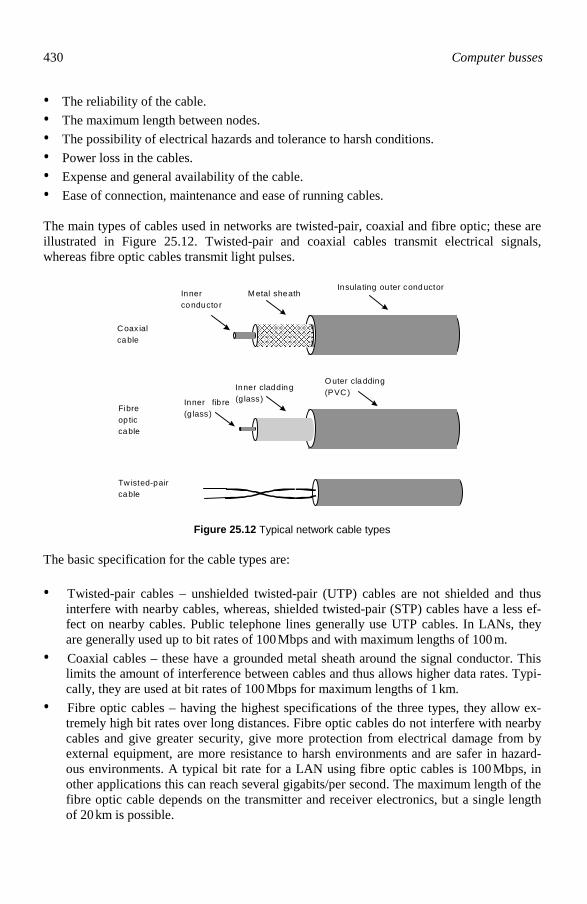
430 Computer busses
• The reliability of the cable. • The maximum length between nodes. • The possibility of electrical hazards and tolerance to harsh conditions. • Power loss in the cables. • Expense and general availability of the cable. • Ease of connection, maintenance and ease of running cables. The main types of cables used in networks are twisted-pair, coaxial and fibre optic; these are illustrated in Figure 25.12. Twisted-pair and coaxial cables transmit electrical signals, whereas fibre optic cables transmit light pulses.
M etal sheath Innerconducto r
Insulating outer conductor
C oax ialcable
Tw isted-paircable
Inner cladding(g lass)Inner fib re
(g lass)
O uter cladding(PVC )
Fibre op ticcable
Figure 25.12 Typical network cable types
The basic specification for the cable types are: • Twisted-pair cables – unshielded twisted-pair (UTP) cables are not shielded and thus
interfere with nearby cables, whereas, shielded twisted-pair (STP) cables have a less ef-fect on nearby cables. Public telephone lines generally use UTP cables. In LANs, they are generally used up to bit rates of 100 Mbps and with maximum lengths of 100 m.
• Coaxial cables – these have a grounded metal sheath around the signal conductor. This limits the amount of interference between cables and thus allows higher data rates. Typi-cally, they are used at bit rates of 100 Mbps for maximum lengths of 1 km.
• Fibre optic cables – having the highest specifications of the three types, they allow ex-tremely high bit rates over long distances. Fibre optic cables do not interfere with nearby cables and give greater security, give more protection from electrical damage from by external equipment, are more resistance to harsh environments and are safer in hazard-ous environments. A typical bit rate for a LAN using fibre optic cables is 100 Mbps, in other applications this can reach several gigabits/per second. The maximum length of the fibre optic cable depends on the transmitter and receiver electronics, but a single length of 20 km is possible.

Networks 431
25.6 Exercises
The following questions are multiple choice. Please select from a to d. 25.6.1 The cable type which offers the highest bit rate is: (a) Fibre optic cable (b) Twisted pair cable (c) Coaxial cable (d) Untwisted pair cable 25.6.2 Which of the following is the main disadvantage of a star network: (a) That the data transmitted between the central server and the
node is relatively high compared to other network topologies (b) That the network is reliant on a central server (c) All nodes compete for the network (d) Nodes can only transmit data once they have a token 25.6.3 Which of the following is the main disadvantage of a ring network: (a) That the data transmitted between the central server and the
node is relatively high compared to other network topologies (b) That the network is reliant on a central server (c) All nodes compete for the network (d) A break in the ring stops data from being transmitted 25.6.4 Which of the following is the main disadvantage of a bus network: (a) Nodes can only transmit data once they have a token (b) That the network is reliant on a central server (c) All nodes compete for the network (d) A break in the ring stops data from being transmitted 25.6.5 On a network which address does a bridge route with: (a) IP address (b) Interrupt address (c) MAC address (d) Source address 25.6.6 On a network which address does a router route with: (a) IP address (b) Interrupt address (c) MAC address (d) Source address 25.6.7 Which of the following best describes a peer-to-peer network:

432 Computer busses
(a) Resources are centralised on a server (b) Local resources, such as memory and processor, are shared between users
over the network (c) Local resources, such as disk drives and printers, are shared between users
over the network (d) Internet connections are allocated centrally 25.6.8 Which of the following best describes a client/server network: (a) Resources are centralised on a server (b) Local resources, such as memory and processor, are shared between users
(c) Local resources, such as disk drives and printers, are shared between users (d) Internet connections are allocated centrally 25.6.9 Explain how peer-to-peer networks differ from server-based networks. When
might peer-to-peer networks be used and how must they be carefully set up. 25.6.10 If possible, set up a peer-to-peer connection between two computers and share
some folders. 25.6.11 Locate a LAN within an organisation, such as a college or university network, and
determine the cables that are used.
25.7 Notes from the author
Many of the great inventions/developments of our time were things that were not really pre-dicted, such as CD-ROMs, RADAR, silicon transistors, fibre optic cables, and, of course, the Internet. The Internet itself is basically an infrastructure of interconnected networks which run a common protocol. The nightmare of interfacing the many computer systems around the world was solved because of two simple protocols: TCP and IP. Without them the Internet would not have evolved so quickly and possibly would not have occurred at all. TCP and IP are excellent protocols as they are simple and can be run over any type of network, on any type of computer system. The Internet is often confused with the World Wide Web (WWW), but the WWW is only one application of the Internet. Others include electronic mail (the No.1 application), file transfer, remote login, and so on. The amount of information transmitted over networks increases by a large factor every year. This is due to local area networks, wide area networks and traffic over the Internet. It is currently estimated that traffic on the Internet doubles every 100 days and that three peo-ple join the Internet every second. This means an eight-fold increase in traffic over a whole year. It is hard to imagine such growth in any other technological area. Imagine if cars were eight times faster each year, or could carry eight times the number of passengers each year (and of course roads and driveways would have to be eight times larger each year). Networks have grown vastly since the 1970s, and most companies now have some form of network. At the beginning of the 1980s, PCs were relatively complex machines to use, and required application programs to be installed locally to their disk drives. Many modern

Networks 433
computers now run their application programs over a network, which makes the administra-tion of the application software must simpler, and also allows users to share their resources. The topology of a network is all-important, as it can severely effect the performance of the network, and can also be used to find network faults. I have run a network for many years and know the problems that can occur if a network grows without any long-term strat-egy. Many users (especially managers) perceive that a network can be expanded to an infi-nite degree. Many also think that new users can simply be added to the network without a thought on the amount of traffic that they are likely to generate, and its effect on other users. It is thus important for network managers to have a short-term, a medium-term and a long-term plan for the network. So, what are the basic elements of a network. I would say: • IP addresses/domain names (but only if the network connects to the Internet or uses
TCP/IP). • A network operating system (such as Microsoft Windows, Novell NetWare, UNIX and
Linux). Many companies run more than one type of network operating system, which causes many problems, but has the advantage of being able to migrate from one network operating system to another. One type of network operating system can also have advan-tages over other types. For example, UNIX is a very robust networking operating system which has good network security and directly supports TCP/IP for all network traffic.
• The cables (twisted-pair, fibre optic or coaxial cables). These directly affect the bit rate of the network, its reliability and the ease of upgrade of the network.
• Network servers, client/server connections and peer-to-peer connections. • Bridges, routers and repeaters. These help to isolate traffic from one network segment to
another. Routers and bridges are always a good long-term investment and help to isolate network traffic and can also isolate segment faults.
The networking topology of the future is likely to evolve around a client/server architecture. With this, server machines run special programs which wait for connections from client ma-chines. These server programs typically respond to networked applications, such as elec-tronic mail, WWW, file transfer, remote login, date/time servers, and so on. Many application programs are currently run over local area networks, but in the future many could be run over wide area networks, or even over the Internet. This means that com-puters would require the minimum amount of configuration and allows the standardisation of programs at a single point (this also helps with bug fixes and updates). There may also be a time when software licensing is charged by the amount of time that a user actually uses the package. This requires applications to be run from a central source (the server). The Internet, networks and increased computing power will have great effects on all ar-eas of life, whether they are in commerce, in industry or in home life. The standardisation of networking technology has allowed for the standardisation of systems, especially in elec-tronic mail, and remote working. The key of this success is the worldwide acceptance of the TCP/IP protocol, which allows different computer systems over the world to communicate, no matter their type, their architecture, or their operating system. The Internet is likely to have a great effect on how companies do business. It is likely that in the coming years that many companies will become reliant on electronic commerce for much of their business, whether it is by direct sales over the Internet or the integration of their financial operation in an electronic form.
434 Computer busses
Electronic commerce involves customers using electronic communications to purchase goods, typically using the Internet. This will change the way that many businesses do busi-ness, and the way that consumers purchase their goods. Society is now moving from a cash based society to a cashless society. Most consumers now use ATMs (Automatic Telling Ma-chines) for cash withdrawals, and debit and credit cards to purchase goods. The future is likely to see an increase in consumers using electronic methods to pay for their goods. An important key to the acceptance of Internet-based purchases is that the must be secure, and cannot be used by criminals to make false purchases, or criminals setting up companies which take payments for incorrect services. Computer networks are a crucial part of many organisations and many users now even have a network connection in their own home. Without networks, there would be no elec-tronic mail, no Internet access and no networked applications. It is one of the fastest growing technological areas and brings benefits to virtually every country in the world. With the in-terconnection of networks to the Internet, the world has truly become a Global Village. For many people, especially children, the first place to search for a given topic is the World Wide Web (WWW). Who would believe the pace of technology over ten short years, such as: • From networks of tens of computers operating at speeds of thousands of bits per second
to networks with thousands of computers operating at billions of bits per second. • From organisations that passed paper documents back and forward, to the totally pa-
perless organisations. • From people who sent one letter each month to people who send tens of electronic mails
every day. • From sending letters around the world which would take days or weeks to be arrive to
the transmission of information around the world within a fraction of a second. • From businesses that relied on central operations to ones that can be distributed around
the world, but can communicate as if they were next door. • From the transmission of memos which could be viewed by people and organisation
which were not meant to the read the message, to the transmission of messages can only be read by the intended destination (and maybe, by space aliens). Not even the CIA can decrypt these messages.
• From written signatures that can be easily forged, to digital signatures which are almost impossible to forge, and not only authenticate the sender but also all of the contents of a message.
These days virtually every computer in a company is networked and networks are key to the effective working of an organisation. Without them, few people could work effectively. They provide us with: • Electronic mail. • Networked application software. • Remote connections. • Shared printers. • Networked video conferencing. • Remote control of remote equipment. • Remote data acquisition. • Shared disk resources.

Ethernet
26.1 Introduction
Most of the computers in business now connect through a LAN and the most commonly used LAN is Ethernet. DEC, Intel and the Xerox Corporation initially developed Ethernet and the IEEE 802 committee has since defined standards for it, the most common of which are Ethernet 2.0 and IEEE 802.3. This section discusses Ethernet technology and the different types of Ethernet. In itself Ethernet cannot make a network and needs some other protocol such as TCP/IP to allow nodes to communicate. Unfortunately, Ethernet in its standard form does not cope well with heavy traffic, but this is offset by the following: • Ethernet networks are easy to plan and cheap to install. • Ethernet network components, such as network cards and connectors, are cheap and well
supported. • It is a well-proven technology, which is fairly robust and reliable. • It is simple to add and delete computers on the network. • It is supported by most software and hardware systems. A major problem with Ethernet is that, because computers must contend to get access to the network, there is no guarantee that they will get access within a given time. This contention also causes problems when two computers try to communicate at the same time – they must both back off and no data can be transmitted. In its standard form Ethernet allows a bit rate of 10 Mbps, but new standards for fast Ethernet systems minimise the problems of contention and also increase the bit rate to 100 Mbps (and even 1 Gbps). Ethernet uses coaxial, fibre optic or twisted-pair cable. Ethernet uses a shared-media, bus-type network topology where all nodes share a com-mon bus. These nodes must then contend for access to the network as only one node can communicate at a time. Data is then transmitted in frames which contain the MAC (media access control) source and destination addresses of the sending and receiving node, respec-tively. The local shared media is known as a segment. Each node on the network monitors the segment and copies any frames addressed to it. Ethernet uses carrier sense, multiple access with collision detection (CSMA/CD). On a CSMA/CD network, nodes monitor the bus (or Ether) to determine if it is busy. A node wishing to send data waits for an idle condition then transmits its message. Unfortunately, collisions can occur when two nodes transmit at the same time, thus nodes must monitor the cable when they transmit. When a collision occurs, both nodes stop transmitting frames and transmit a jamming signal. This informs all nodes on the network that a collision has oc-curred. Each of the nodes involved in the collision then waits a random period of time before attempting a retransmission. As each node has a random delay time then there can be a pri-oritisation of the nodes on the network, as illustrated in Figure 26.1.
26

436 Computer busses
Each node on the network must be able to detect collisions and be capable of transmitting and receiving simultaneously. These nodes either connect onto a common Ethernet connec-tion or can connect to an Ethernet hub. Nodes thus contend for the network and are not guar-anteed access to it. Collisions generally slow the network.
CSMA/CDEthernet uses carrier sense, multiple access with collision detection (CSMA/CD). Nodes monitor the bus (or Ether) to determine if it is busy. A node wishing to send data waits for an idle condition then transmits its message. Collisions can occur when two nodes transmit at the same time, thus nodes must monitor the cable when they transmit. When a collision occurs, both nodes stop transmitting frames and transmit a jamming signal. This informs all nodes on the network that a collision has occurred. Each of the nodes involved in the collision then waits a random period of time before attempting a re-transmission. As each node has a random delay time then there
can be a prioritisation of the nodes on the network.
Two nodes transmitat the same time
Node detect therehas been a collision
Nodes transmit ajamming signal
Nodes wait a randomperiod before retransmitted
Common bus
All computers have access toa common bus at the same time
CSMA/CDEthernet uses carrier sense, multiple access with collision detection (CSMA/CD). Nodes monitor the bus (or Ether) to determine if it is busy. A node wishing to send data waits for an idle condition then transmits its message. Collisions can occur when two nodes transmit at the same time, thus nodes must monitor the cable when they transmit. When a collision occurs, both nodes stop transmitting frames and transmit a jamming signal. This informs all nodes on the network that a collision has occurred. Each of the nodes involved in the collision then waits a random period of time before attempting a re-transmission. As each node has a random delay time then there
can be a prioritisation of the nodes on the network.
Two nodes transmitat the same time
Node detect therehas been a collision
Nodes transmit ajamming signal
Nodes wait a randomperiod before retransmitted
Common bus
All computers have access toa common bus at the same time
Common bus
All computers have access toa common bus at the same time
Figure 26.1 Ethernet transmission
26.2 IEEE standards
The IEEE are the main standards organization for LANs and they refer to the standard for Ethernet as CSMA/CD. Figure 26.2 shows how the IEEE standards for CSMA/CD fit into the OSI model. The two layers of the IEEE standards correspond to the physical and data link layers of the OSI model. On Ethernet networks, most hardware complies with IEEE 802.3 standard. The MAC layer allows many nodes to share a single communication chan-nel. It also adds the start and end frame delimiters, error detection bits, access control infor-mation, and source and destination addresses. Each frame also has an error detection scheme known as cyclic redundancy check (CRC).
LLC (IEE E 802.2)Data link
Physica lM edia access
control (IEE E 802.3)
Figure 26.2 Standards for IEEE 802 LANs
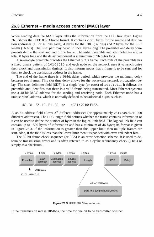
Ethernet 437
26.3 Ethernet – media access control (MAC) layer
When sending data the MAC layer takes the information from the LLC link layer. Figure 26.3 shows the IEEE 802.3 frame format. It contains 2 or 6 bytes for the source and destina-tion addresses (16 or 48 bits each), 4 bytes for the CRC (32 bits) and 2 bytes for the LLC length (16 bits). The LLC part may be up to 1500 bytes long. The preamble and delay com-ponents define the start and end of the frame. The initial preamble and start delimiter are, in total, 8 bytes long and the delay component is a minimum of 96 bytes long. A seven-byte preamble precedes the Ethernet 802.3 frame. Each byte of the preamble has a fixed binary pattern of 10101010 and each node on the network uses it to synchronise their clock and transmission timings. It also informs nodes that a frame is to be sent and for them to check the destination address in the frame. The end of the frame there is a 96-bit delay period, which provides the minimum delay between two frames. This slot time delay allows for the worst-case network propagation de-lay. The start delimiter field (SDF) is a single byte (or octet) of 10101011. It follows the preamble and identifies that there is a valid frame being transmitted. Most Ethernet systems use a 48-bit MAC address for the sending and receiving node. Each Ethernet node has a unique MAC address, which is normally defined as hexadecimal digits, such as: 4C - 31 - 22 - 10 - F1 - 32 or 4C31 : 2210: F132. A 48-bit address field allows 248 different addresses (or approximately 281 474 976 710 000 different addresses). The LLC length field defines whether the frame contains information or it can be used to define the number of bytes in the logical link field. The logical link field can contain up to 1500 bytes of information and has a minimum of 46 bytes; its format is given in Figure 26.3. If the information is greater than this upper limit then multiple frames are sent. Also, if the field is less than the lower limit then it is padded with extra redundant bits. The 32-bit frame check sequence (or FCS) is an error detection scheme. It is used to de-termine transmission errors and is often referred to as a cyclic redundancy check (CRC) or simply as a checksum.
7 bytes 1 byte 6 bytes 6 bytes
46 to 1500 bytes
4 bytes 96 bits
10101...0101010
10101011
2 bytes
DelayFCSLengthSourceaddress
Destinationaddress
StartdelimiterPreamble
Data field (Logical Link Control)
Figure 26.3 IEEE 802.3 frame format
If the transmission rate is 10Mbps, the time for one bit to be transmitted will be:

438 Computer busses
ns 100s 1010
1ratebit 1
6 =×
==T
Thus the maximum and minimum times to transmit a frame will be: ( ) ms 2.1ns 1008124150026617max =××+++++++=T ( ) μs 067.0ns 10081244626617min =××+++++++=T It may be assumed that an electrical signal propagates at about half the speed of light (c=3×10⁸m/s). Thus, the time for a bit to propagate a distance of 500 m is:
sspeeddistT m µ33.3
105.1500
8500 =×
==
by which time, the number of bits transmitted will be:
33.33100
33.3ed transmittbits ofNumber 500 ===
nss
TT
bit
m µ
Thus, if two nodes are separated by 500m then it will take more than 33 bits to be transmitted before a node can determine if there has been a collision of the line, as illustrated in Figure 26.4. If the propagation speed is less that this, it will take even longer. This shows the need for the preamble and the requirement for a maximum segment length.
For a distance of 500m, there are approximately 33.33 bits transmitted before the sender can sense
a collision
Figure 26.4 Bits transmitted before a collision is detected
26.3.1 Ethernet II
The first standard for Ethernet was Ethernet I. Most currently available systems implement either Ethernet II or IEEE 802.3 (although most networks are now defined as being IEEE 802.3 compliant). An Ethernet II frame is similar to the IEEE 802.3 frame; it consists of eight bytes of preamble, six bytes of destination address, six bytes of source address, two bytes of frame type, between 46 and 1500 bytes of data, and four bytes of the frame check sequence field.

Ethernet 439
When the protocol is IPX/SPX the frame type field contains the bit pattern 1000 0001 0011 0111, but when the protocol is TCP/IP the type field contains 0000 1000 0000 0000.
26.4 IEEE 802.2 and Ethernet SNAP
The LLC is embedded in the Ethernet frame and is defined by the IEEE 802.2 standard. Fig-ure 26.5 illustrates how the LLC field is inserted into the IEEE 802.3 frame. The DSAP and SSAP fields define the types of network protocol used. A SAP code of 1110 0000 identifies the network operating system layer as NetWare, whereas 0000 0110 identifies the TCP/IP protocol. These SAP numbers are issued by the IEEE. The control field is, among other things, for the sequencing of frames. In some cases, it was difficult to modify networks to be IEEE 802 compliant. Thus, an alternative method was to identify the network protocol, known as Ethernet SNAP (subnet-work access protocol). This was defined to ease the transition to the IEEE 802.2 standard and is illustrated in Figure 26.6. It simply adds an extra two fields to the LLC field to define an organisation ID and a network layer identifier. NetWare allows for either Ethernet SNAP or Ethernet 802.2 (as Novell used Ethernet SNAP to translate to Ethernet 802.2). Non-compliant protocols are identified with the DSAP and SSAP code of 1010 1010, and a control code of 0000 0011. After these fields come • Organization ID – which indicates where the company that developed the embedded
protocol belongs. If this field contains all zeros it indicates a non company-specific ge-neric Ethernet frame.
• EtherType field – which defines the networking protocol. A TCP/IP protocol uses 0000 1000 0000 0000 for TCP/IP, whereas NetWare uses 1000 0001 0011 0111. NetWare frames adhering to this specification are known as NetWare 802.2 SNAP.
Preamble Startdelimiter
Destinationaddress
Sourceaddress
Logicallink control FCS Delay
7 bytes 1 byte 6 bytes 6 bytes 46 to 1500 bytes 4 bytes 96 bytes
10101...0101010
10101011
Length
2 bytes
Destinationservice accesspoint (DSAP)
Sourceservice accesspoint (SSAP)
Controlfield
DATA
1/2 bytes1 byte1 byte
Figure 26.5 Ethernet IEEE 802.3 frame with LLC

440 Computer busses
Preamble Startdelimiter
Destinationaddress
Sourceaddress
Logicallink control FCS Delay
7 bytes 1 byte 6 bytes 6 bytes 46 to 1500 bytes 4 bytes 96 bytes
10101...0101010
10101011
Length
2 bytes
1010 1010 DATA
3 bytes
1010 1010 0000 0011 OrganizationID EtherType
2 bytes
SNAP header
Figure 26.6 Ethernet IEEE 802.3 frame with LLC containing SNAP header
26.4.1 LLC protocol
The 802.3 frame provides some of the data link layer functions, such as node addressing (source and destination MAC addresses), the addition of framing bits (the preamble) and error control (the FCS). The rest of the functions of the data link layer are performed with the control field of the LLC field; these functions are: • Flow and error control – each data frame sent has a frame number. A control frame is
sent from the destination to a source node informing that it has or has not received the frames correctly.
• Sequencing of data – large amounts of data are sliced and sent with frame numbers. The spliced data is then reassembled at the destination node.
Figure 26.7 shows the basic format of the LLC frame. There are three principal types of frame: information, supervisory and unnumbered. An information frame contains data, a supervisory frame is used for acknowledgement and flow control, and an unnumbered frame is used for control purposes. The first two bits of the control field determine which type of frame it is. If they are 0X (where X is a don’t care) then it is an information frame, 10 speci-fies a supervisory frame and 11 specifies an unnumbered frame.
1 2 3 4 5 6 7 8 9 10 11 12 13 14 15 16
DSAP
1 byte 1 byte 1/2 byte(s) ≥1 byte
SSAP Control Data
0 Send seq. no(0-127) P 0Receive seq. no
(0-127)Informationframe
1 S P 0Receive seq. no(0-127)
Supervisoryframe0
RR, RNRor REJ
Figure 26.7 LLC frame format

Ethernet 441
An information frame contains a send sequence number in the control field which ranges from 0 to 127. Each information frame has a consecutive number, N(S) (note that there is a roll-over from frame 127 to frame 0). The destination node acknowledges that it has re-ceived the frames by sending a supervisory frame. The function of the supervisory frame is specified by the 2-bit S field. This can either be set to receiver ready (RR), receiver not ready (RNR) or reject (REJ). If an RNR function is set then the destination node acknowledges that all frames up to the number stored in the receive sequence number N(R) field were received correctly. An RNR function also acknowledges the frames up to the number N(R), but in-forms the source node that the destination node wishes to stop communicating. The REJ function specifies that frame N(R) has been rejected and all other frames up to N(R) are ac-knowledged.
26.5 OSI and the IEEE 802.3 standard
Ethernet fits into the data link and the physical layer of the OSI model. These two layers only deal with the hardware of the network. The data link layer splits into two parts: the LLC and the MAC layer. The IEEE 802.3 standard splits into three sublayers: • MAC (media access control). • Physical signalling (PLS). • Physical media attachment (PMA). The interface between PLS and PMA is called the attachment unit interface (AUI) and the interface between PMA and the transmission media is called the media dependent interface (MDI). This grouping into modules allows Ethernet to be very flexible and to support a number of bit rates, signalling methods and media types. Figure 26.8 illustrates how the lay-ers interconnect.
PLS
PMA
MDI
MAC
Medium
AUI
MAU
Figure 26.8 Organisation of the IEEE 802.3 standard

442 Computer busses
26.5.1 Media access control (MAC)
The CSMA/CD function is implemented in the MAC layer. The functions of the MAC layers are: • When sending frames – receive frames from LLC; control whether the data fills the LLC
data field, if not add redundant bits; make the number of bytes an integer, and calculate the FCS; add the preamble, SFD and address fields to the frame; send the frame to the PLS in a serial bit stream.
• When receiving frames – receive one frame at a time from the PLS in a serial bit stream; check whether the destination address is the same as the local node; ensure the frame contains an integer number of bytes and the FCS is correct; remove the preamble, SFD, address fields, FCS and remove redundant bits from the LLC data field; send the data to the LLC.
• Avoid collisions when transmitting frames and keep the right distance between frames by not sending when another node is sending; when the medium is free, wait a specified period before starting to transmit.
• Handle any collision that appears by sending a jam signal; generate a random number and back off from sending during that random time.
26.5.2 Physical signalling (PLS) and physical medium attachment (PMA)
PLS defines transmission rates, types of encoding/decoding and signalling methods. In PMA a further definition of the transmission media is accomplished, such as coaxial, fibre or twisted-pair. PMA and MDI together form the media attachment unit (MAU), often known as the transceiver.
26.6 Ethernet transceivers
Ethernet requires a minimal amount of hardware. The cables used to connect it are typically either unshielded twisted-pair cable (UTP) or coaxial cables. These cables must be termi-nated with their characteristic impedance, which is 50Ω for coaxial cables and 100Ω for UTP cables. Each node has transmission and reception hardware to control access to the cable and also to monitor network traffic. The transmission/reception hardware is called a transceiver (short for transmitter/receiver) and a controller builds up and strips down the frame. For 10 Mbps Ethernet, the transceiver builds the transmitted bits at a rate of 10 Mbps – thus the time for one bit is 1/10×1 06, which is 0.1µs (100 ns). The Ethernet transceiver transmits onto a single ether. When there are no nodes transmit-ting, the voltage on the line is +0.7 V. This provides a carrier sense signal for all nodes on the network, it is also known as the heartbeat. If a node detects this voltage then it knows that the network is active and there are no nodes currently transmitting. Thus, when a node wishes to transmit a message it listens for a quiet period. Then, if two or more transmitters transmit at the same time, a collision results. When they detect a colli-sion, each node transmits a ‘jam’ signal. The nodes involved in the collision then wait for a random period of time (ranging from 10 to 90 ms) before attempting to transmit again. Each node on the network also awaits for a retransmission. Thus, collisions are inefficient in net-works as they stop nodes from transmitting. Transceivers normally detect collisions by moni-

Ethernet 443
toring the DC (or average) voltage on the line. When transmitting, a transceiver unit transmits the preamble of consecutive 1s and 0s. The coding used is a Manchester coding, which represents a 0 as a high to a low voltage tran-sition and a 1 as a low to high voltage transition. A low voltage is represented by –0.7 V and a high is +0.7 V. Thus, when the preamble is transmitted the voltage changes between +0.7V and –0.7 V; as illustrated in Figure 26.9. If after the transmission of the preamble no collisions are detected then the rest of the frame is sent.
Idle Preamble
+0.7 V
0.1 µs
1 0 1 0 1
–0.7 V
Idle Figure 26.9 Ethernet digital signal
26.7 Ethernet types
The six main types of standard Ethernet are: • Standard, or thick-wire, Ethernet (10BASE5). • Thinnet, or thin-wire Ethernet, or Cheapernet (10BASE2). • Twisted-pair Ethernet (10BASE-T). • Optical fibre Ethernet (10BASE-FL). • Fast Ethernet (100BASE-TX and 100VG-Any LAN). • Gigabit Ethernet (1000BASE-SX, 1000BASE-T, 1000BASE-LX and 1000BASE-CX). The thin- and thick-wire types connect directly to an Ethernet segment; these are shown in Figure 26.10 and Figure 26.11. Standard Ethernet, 10BASE5, uses a high specification cable (RG-50) and N-type plugs to connect the transceiver to the Ethernet segment. A node con-nects to the transceiver using a 9-pin D-type connector and a vampire (or bee-sting) connec-tor can be used to clamp the transceiver to the backbone cable. Thin-wire, or Cheapernet, uses a lower specification cable (it has a lower inner conductor diameter). The cable connector required is also of a lower specification, that is, BNC rather than N-type connectors. In standard Ethernet the transceiver unit is connected directly onto the backbone tap. On a Cheapernet network the transceiver is integrated into the node. Most modern Ethernet connections are to a 10BASE-T hub, which connects UTP cables to the Ethernet segment. A RJ-45 connector is used for 10BASE-T. The fibre optic type, 10BASE-FL, allows long lengths of interconnected lines, typically up to 2 km. They use ei-ther SMA connectors or ST connectors. SMA connectors are screw-on types whereas ST connectors are push-on. Table 26.1 shows the basic specifications for the different types.

444 Computer busses
10BASE510BASE5
RG-50 backbonecable
N-typeT-connector
9-pin D-typeconnector (AUI)
9-pin D-typeconnector (AUI)
Vampire(or bee-sting)tap
Figure 26.10 Ethernet connections for thick Ethernet
BNCT-connector
BNC connector
10BASE2
10BASE-T
Hub
RG-50 backbonecable
Twisted-paircable
RJ-45connector
Figure 26.11 Ethernet connections for thin Ethernet and 10BASE-T
Table 26.1 10BASE network parameters
Parameter 10BASE5 10BASE2 10BASE-T Common name Standard or thick-wire
Ethernet Thinnet or thin-wire Ethernet
Twisted-pair Ethernet
Data rate 10 Mbps 10 Mbps 10 Mbps Maximum segment length
500 m 200 m 100 m
Maximum nodes on a segment
100 30 3
Maximum number of repeaters
2 4 4
Maximum nodes per network
1024 1024
Minimum node spacing 2.5 m 0.5 m no limit Location of transceiver electronics
located at the cable connection
integrated within the node
in a hub
Typical cable type
RG-50 (0.5 in diameter)
RG-6 (0.25 i n diameter)
UTP cables
Connectors N-type BNC RJ-45/ Telco Cable impedance
50 Ω 50 Ω 100 Ω

Ethernet 445
26.8 Twisted-pair hubs
Twisted-pair Ethernet (10BASE-T) nodes normally connect to the backbone using a hub, as illustrated in Figure 26.12. Connection to the twisted-pair cable is via an RJ-45 connector. The connection to the backbone can either be to thin or thick Ethernet. Hubs are also stack-able, with one hub connected to another. This leads to concentrated area networks (CANs) and limits the amount of traffic on the backbone. Twisted-pair hubs normally improve net-work performance. 10BASE-T uses two twisted-pair cables, one for transmit and one for receive. A collision occurs when the node (or hub) detects that it is receiving data when it is currently transmit-ting data.
10BASE-Thub
Ethernet backbone
Figure 26.12 10BASE-T connection
26.9 100Mbps Ethernet
Standard 10 Mbps Ethernet does not perform well when many users are running multimedia applications. Two improvements to the standard are Fast Ethernet and 100VG-AnyLAN. The IEEE has defined standards for both of them, IEEE 802.3u for Fast Ethernet and 802.12 for 100VG-AnyLAN. They are supported by many manufacturers and use bit rates of 100 Mbps. This gives at least 10 times the performance of standard Ethernet. New standards relating to 100 Mbps Ethernet are now becoming popular: • 100BASE-TX (twisted-pair) – which uses 100 Mbps over two pairs of Cat-5 UTP cable
or two pairs of Type 1 STP cable. • 100BASE-T4 (twisted-pair) – which is the physical layer standard for 100 Mbps over
Cat-3, Cat-4 or Cat-5 UTP. • 100VG-AnyLAN (twisted-pair) – which uses 100 Mbps over two pairs of Cat-5 UTP
cable or two pairs of Type 1 STP cable.

446 Computer busses
• 100BASE-FX (fiber-optic cable) – which is the physical layer standard for 100 Mbps over fiber-optic cables.
Fast Ethernet, or 100BASE-T, is simply 10BASE-T running at 10 times the bit rate. It is a natural progression from standard Ethernet and thus allows existing Ethernet networks to be easily upgraded. Unfortunately, as with standard Ethernet, nodes contend for the network, reducing the network efficiency when there are high traffic rates. Also, as it uses collision detect, the maximum segment length is limited by the amount of time for the farthest nodes on a network to properly detect collisions. On a Fast Ethernet network with twisted-pair cop-per cables this distance is 100 m, and for a fibre-optic link, it is 400 m. Table 26.2 outlines the main network parameters for Fast Ethernet.
Table 26.2 Fast Ethernet network parameters
100BASE-TX 100VG-AnyLAN Standard IEEE 802.3u IEEE 802.12
Bit rate 100 Mbps 100 Mbps
Actual throughput up to 50 Mbps up to 96 Mbps
Maximum distance (hub to node)
100 m (twisted-pair, CAT-5) 400 m (fiber)
100 m (twisted-pair, CAT-3) 200 m (twisted-pair, CAT-5) 2 km (fibre)
Scaleability none up to 400 Mbps
Advantages Easy migration from 10BASE-T
greater throughput, greater distance
As 100BASE-TX standards are compatible with 10BASE-TX networks then the network al-lows both 10 Mbps and 100 Mbps bit rates on the line. This makes upgrading simple, as the only additions to the network are dual-speed interface adapters. Nodes with the 100 Mbps capabilities can communicate at 100 Mbps, but they can also communicate with slower nodes, at 10 Mbps. The basic rules of a 100BASE-TX network are:
• The network topology is a star network and there must be no loops. • Cat-5 cable is used. • Up to two hubs can be cascaded in a network. • Each hub is the equivalent of 5 m in latency. • Segment length is limited to 100 m. • Network diameter must not exceed 205 m.
26.9.1 100BASE-T4
100BASE-T4 allows the use of standard Cat-3 cables. These contain eight wires made up of four twisted-pairs. 100BASE-4T uses all of the pairs to transmit at 100 Mbps. This differs from 10BASE-T in that 10BASE-T uses only two pairs, one to transmit and one to receive.

Ethernet 447
100BASE-T allows compatibility with 10BASE-T in that the first two pairs (Pair 1 and Pair 2) are used in the same way as 10BASE-T connections. 100BASE-T then uses the other two pairs (Pair 3 and Pair 4) with half-duplex links between the hub and the node. The connec-tions are illustrated in Figure 26.13.
26.9.2 Line code
100BASE-4T uses four separate Cat-3 twisted-pair wires. The maximum clock rate that can be applied to Cat-3 cable is 30 Mbps. Thus, some mechanism must be devised which reduces the line bit rate to under 30 Mbps but gives a symbol rate of 100 Mbps. This is achieved with a three-level code (+, – and 0) and is known as 8B6T. This code converts eight binary digits into six ternary symbols.
Node Hub
Tx Rx
Rx Tx
Tx Rx
Rx Tx
Pair 1
Pair 2
Pair 3
Pair 4
Com patible with10BASE
Figure 26.13 100BASE-4T connections
The first six codes are: Data byte Code Data byte Code Data byte Code 00000000 –+0 0–+ 00000001 0–+ –+0 00000010 0–+ 0–+
00000011 0–+ +0– 00000100 –+0 +0– 00001001 +0– –+0
Thus, the bit sequence 00000000 will be coded as a negative voltage, a positive voltage, a zero voltage, a zero voltage, a negative voltage and a positive voltage. The maximum base frequency for a 100 Mbps signal will be produced when the input bitstream is 010101010 …01010. As each bit lasts 10 ns then the period between consecutive levels is 20 ns. Thus, the minimum frequency contained will be 50 MHz. This is greater than the bandwidth of Cat-3 cable, so it would not pass through the cable. Apart from reducing the frequencies with the digital signal, the 8B6T code has the advan-tage of reducing the DC content of the signal. Most of the codes contain the same number of positive and negative voltages. This is because only 256 of the possible 729 (36) codes are actually used. The codes are also chosen to have at least two transitions in every code word, thus the clock information is embedded into the signal. Unfortunately, it is not possible to have all codes with the same number of negative volt-

448 Computer busses
ages as positive voltages. Thus, there are some codes that have a different number of nega-tives and positives, these include: 0100 0001+0–00+ 0111 1001+++–0– Most transceiver circuits use a transformer to isolate the external equipment from the com-puter equipment. These transformers do not allow the passage of DC current. Thus if the line code has a sequence which consecutively has more positives than negatives, the DC current will move away from its zero value. As this does not pass across the transformer, the receive bitstream on the output of the transformer can reduce the amplitude of the received signal (and may thus cause errors). This phenomenon is known as DC wander. A code that has one more positive level than the negative levels is defined as having a weighing of +1. The technique used to overcome this is to invert consecutive codes that have a weighing of +1. For example, suppose the line code were
+0++–– ++0+–– +++––0 +++––0 it would actually be coded as
+0 ++– – – – 0 – ++ +++––0 –––++0
The receiver detects the –1 weighted codes as an inverted pattern.
26.9.3 100VG-AnyLAN
The 100VG-AnyLAN standard (IEEE 802.12) was developed mainly by Hewlett Packard and overcomes the contention problem by using a priority-based round-robin arbitration method, known as demand priority access method (DPAM). Unlike Fast Ethernet, nodes always connect to a hub which regularly scans its input ports to determine whether any nodes have requests pending. 100VG-AnyLAN has the great advantage over 100BASE in that it supports both IEEE 802.3 (Ethernet) and IEEE 802.5 (Token Ring) frames and can thus integrate well with exist-ing 10BASET and Token Ring networks. 100VG-AnyLAN has an in-built priority mechanism with two priority levels: a high pri-ority request and a normal priority request. A normal priority request is used for non real-time data, such as data files, and so on. High priority requests are used for real-time data, such as speech or video data. At present, there is limited usage of this feature and there is no support mechanism for this facility after the data has left the hub. 100VG-AnyLAN allows up to seven levels of hubs (i.e. one root and six cascaded hubs) with a maximum distance of 150 m between nodes. Unlike other forms of Ethernet, it allows any number of nodes to be connected to a segment.
Connections
100BASE-TX, 100BASE-T4 and 100VG-AnyLAN use the RJ-45 connector, which has eight connections. 100BASE-TX uses pairs 2 and 3, whereas 100BASE-T4 and 100VG-AnyLAN use pairs 1, 2, 3 and 4. The connections for the cables are defined in Table 26.3. The white/orange colour identifies the cable which is white with an orange stripe, whereas or-ange/white identifies an orange cable with a white stripe.
Ethernet 449
Table 26.3 Cable connections for 100BASE-TX
Pin Cable colour Cable colour Pair 1 white/orange white/orange Pair 4 2 orange/white orange/white Pair 4 3 white/green white/green Pair 3 4 blue/white blue/white Pair 3 5 white/blue white/blue Pair 1 6 green/white green/white Pair 1 7 white/brown white/brown Pair 2 8 brown/white brown/white Pair 2
Migration to fast Ethernet
If an existing network is based on standard Ethernet then, in most cases, the best network upgrade is either to fast Ethernet or 100VG-AnyLAN. As the protocols and access methods are the same, there is no need to change any of the network management software or applica-tion programs. The upgrade path for Fast Ethernet is simple and could be:
• Upgrade high data rate nodes, such as servers or high-powered workstations to Fast Ethernet.
• Gradually upgrade NICs (network interface cards) on Ethernet segments to cards which support both 10BASE-T and 100BASE-T. These cards automatically detect the trans-mission rate to give either 10 or 100 Mbps.
The upgrade path to 100VG-AnyLAN is less easy as it relies on hubs and, unlike Fast Ethernet, most NICs have different network connectors, one for 10BASE-T and the other for 100VG-AnyLAN (although it is likely that more NICs will have automatic detection). A possible path could be:
• Upgrade high data rate nodes, such as servers or high-powered workstations to 100VG-AnyLAN.
• Install 100VG-AnyLAN hubs. • Connect nodes to 100VG-AnyLAN hubs and change over connectors. It is difficult to assess the performance differences between Fast Ethernet and 100VG-AnyLAN. Fast Ethernet uses a well-proven technology, but suffers from network contention. 100VG-AnyLAN is a relatively new technology and the handshaking with the hub increases delay time. The maximum data throughput of a 100BASE-TX network is limited to around 50 Mbps, whereas 100VG-AnyLAN allows rates up to 96 Mbps. 100VG-AnyLAN allows possible upgrades to 400 Mbps.

450 Computer busses
26.10 Comparison of fast Ethernet other technologies
Table 26.4 compares fast Ethernet with other types of networking technologies.
Table 26.4 Comparison of fast Ethernet with other networking technologies
Feature 100VG-AnyLAN (Cat 3, 4, or 5)
100BASE-T (TX/FX/T4)
FDDI ATM Gigabit Ethernet (802.3z)
Maximum segment length
100 m 100 m (Cat-5) 412 m (Fibre)
2000 m 200 m (Cat-5) 2000 m (Fibre)
100 m (Cat 5) 1k m (Fibre)
Maximum network diameter with repeater(s)
6000 m 320 m 100 km N/A To be determined by the standard
Bit rate
100 Mbps 100 Mbps 100 Mbps 155 Mbps 1 Gbps
Media access method
Demand priority CSMA/CD Token passing
PVC/SVC CSMA/CD
Maximum nodes on each domain
1024 Limited by hub
500
N/A To be determined
Frame type
Ethernet and Token Ring
Ethernet 802.5 53-byte cell Ethernet
Multimedia support
FDDI-I ( ) FDDI-II ( )
YES (with 802.1p)
Integration with 10BASE2
Yes with bridges, switches and routers
Yes with switches
Yes with routers and switches
Yes with routers or switches
Yes with 10/100 Mbps switching
Relative cost Low
Low
Medium
High
Medium
Relative complexity
Low Low Medium High Low
26.10.1 Switching technology
A switch uses store-and-forward packets to switch between ports. The main technologies used are:
• Shared bus – this method uses a high-speed backplane to interconnect the switched ports. It is frequently used to build modular switches that give a large number of ports,
Ethernet 451
and to interconnect multiple LAN technologies, such as FDDI, 100VG-AnyLAN, 100BASE-T, and ATM.
• Shared memory – these use a common memory area (several megabytes) in which data is passed between the ports. It is very common in low-cost, small-scale switches and has the advantage that it can cope with different types of network, which are operating at dif-ferent speeds. The main types of memory allocation are:
• Pooled memory – memory is allocated as it is needed by the ports from a common
memory pool. • Dedicated shared memory – memory is fixed and shared by a single pair of I/O ports. • Distributed memory – memory is fixed and dedicated to each port.
26.11 Switches and switching hubs
A switch is a very fast, low-latency, multiport bridge that is used to segment LANs. They are typically also used to increase communication rates between segments with multiple parallel conversations and also communication between technologies (such as between FDDI and 100BASE-TX). A 4-port switching hub is a repeater that contains four distinct network segments (as if there were four hubs in one device). Through software, any of the ports on the hub can di-rectly connect to any of the four segments at any time. This allows for a maximum capacity of 40 Mbps in a single hub. Ethernet switches overcome the contention problem on normal CSMA/CD networks. They segment traffic by giving each connect a guaranteed bandwidth allocation. Figure 26.14 and Figure 26.15 show the two types of switches; their main features are: • Desktop switch (or workgroup switch) – These connect directly to nodes. They are eco-
nomical with fixed configurations for end-node connections and are designed for stand-alone networks or distributed workgroups in a larger network.
• Segment switch – These connect both 10 Mbps workgroup switches and 100 Mbps inter-connect (backbone) switches that are used to interconnect hubs and desktop switches. They are modular, high-performance switches for interconnecting workgroups in mid- to large-size networks.
26.11.1 Segment switch
A segment switch allows simultaneous communication between any client and any server. A segment switch can simply replace existing Ethernet hubs. Figure 26.15 shows a switch with five ports each transmitting at 10 Mbps; this allows up to five simultaneous connections giv-ing a maximum aggregated bandwidth of 50 Mbps. If the nodes support 100 Mbps communi-cation then the maximum aggregated bandwidth will be 500 Mbps. To optimise the network, nodes should be connected to the switch that connects to the server with which it most often communicates. This allows for a direct connection with that server.

452 Computer busses
LocalserverLocal
printer
Workgroupnodes
Desktop switch
LocalserverLocal
printer
Workgroupnodes
Desktop switch
Main server
Network backbone connection
Segment switches allowsimultaneous communicationbetween any client and anyserver.
Segment switches allowsimultaneous communicationbetween any client and anyserver.
Store-and-forward switchesminimise collisions and theycan store Ethernet frames andretransmit them when segmentis quiet.
Store-and-forward switchesminimise collisions and theycan store Ethernet frames andretransmit them when segmentis quiet.
Figure 26.14 Desktop switch
Switch
Server
External connection (uses store-and-forward for external connection)
Switch connects any of the inputsegments directly to another
Hub Hub Hub
Server
Figure 26.15 Segment switch
26.11.2 Desktop switch
A desktop switch can simply replace an existing 10BASET/100BASET hub. It has the ad-vantage that any of the ports can connect directly to any other. In the network in Figure

Ethernet 453
26.14, any of the computers in the local workgroup can connect directly to any other, or to the printer, or the local disk drive. This type of switch works well if there is a lot of local traffic, typically between a local server and local peripherals.
26.11.3 Store-and-forward switching
Store-and-forwarding techniques have been used extensively in bridges and routers, and are now used with switches. It involves reading the entire Ethernet frame, before forwarding it, with the required protocol and at the correct speed, to the destination port. This has the ad-vantages of: • Improved error check – Bad frames are blocked from entering a network segment. • Protocol filtering – Allows the switch to convert from one protocol to another. • Speed matching – Typically, for Ethernet, reading at 10 Mbps or 100 Mbps and transmit-
ting at 100 Mbps or 10 Mbps. Also, can be used for matching between ATM (155 Mbps), FDDI (100Mbps), Token Ring (4/16 Mbps) and Ethernet (10/100 Mbps).
The main disadvantage is: • System delay – As the frame must be totally read before it is transmitted there is a delay
in the transmission. The improvement in error checking normally overcomes this disad-vantage.
26.12 Network interface card design
When receiving data, the network interface card (NIC) copies all data transmitted on the network, decodes it and transfers it to the computer. An Ethernet NIC contains three parts: • Physical medium interface – the physical medium interface corresponds to the PLS and
PMA in the standard and is responsible for the electrical transmission and reception of data. It consists of two parts: the transceiver, which receives and transmits data from or onto the transmission media; and a code converter that encodes/decodes the data. It also recognises a collision on the media.
• Data link controller – the controller corresponds to the MAC layer. • Computer interface. It can be split into four main functional blocks: • Network interface. • Manchester decoder. • Memory buffer. • Computer interface.
26.12.1 Network interface
The network interface must listen, recreate the waveform transmitted on the cable into a digi-

454 Computer busses
tal signal and transfer the digital signal to the Manchester decoder. The network interface consists of three parts: • BNC/RJ-45 connector. • Reception hardware – the reception hardware translates the waveforms transmitted on
the cable to digital signals then copies them to the Manchester decoder. • Isolator – the isolator is connected directly between the reception hardware and the rest
of the Manchester decoder; it guarantees that no noise from the network affects the com-puter, and vice versa (as it isolates ground levels).
The reception hardware is called a receiver and is the main component in the network inter-face. It acts as an earphone, listening and copying the traffic on the cable. Unfortunately, the Ether and transceiver electronics are not perfect. The transmission line contains resistance and capacitance which distort the shape of the bit stream transmitted onto the Ether. Distor-tion in the system causes pulse spreading, which leads to intersymbol interference. There is also a possibility of noise affecting the digital pulse as it propagates through the cable. Therefore, the receiver also needs to recreate the digital signal and filter noise. Figure 26.16 shows a block diagram of an Ethernet receiver. The received signal goes through a buffer with high input impedance and low capacitance to reduce the effects of loading on the coaxial cable. An equaliser passes high frequencies and attenuates low fre-quencies from the network, flattening the network passband. A 4-pole Bessel low-pass filter provides the average dc level from the received signal. The quench circuit activates the line driver only when it detects a true signal. This prevents noise activating the receiver.
Low-pass filter
Receive equaliser
Squelch
RX+ RX–
Data buffer
GND
RXI
Line driver
GND is –9V (isolated) RX is receive output RXI is network signal receiver
Figure 26.16 Ethernet receiver block diagram
26.12.2 Manchester decoder
Manchester coding has the advantage of embedding timing (clock) information within the transmitted bits. A positively edged pulse (low to high) represents a 1 and a negatively edged pulse (high to low) a 0, as shown in Figure 26.17. Another advantage of this coding method is that the average voltage is always zero when used with equal positive and negative voltage levels. Figure 26.18 is an example of transmitted bits using Manchester encoding. The receiver passes the received Manchester-encoded bits through a low-pass filter. This extracts the low-est frequency in the received bit stream, i.e. the clock frequency. With this clock the receiver

Ethernet 455
can then determine the transmitted bit pattern.
‘1’ ‘0’
Figure 26.17 Manchester encoding
For Manchester decoding, the Manchester-encoded signal is first synchronised to the re-ceiver (called bit synchronisation). A transition in the middle of each bit cell is used by a clock recovery circuit to produce a clock pulse in the center of the second half of the bit cell. In Ethernet the bit synchronisation is achieved by deriving the clock from the preamble field of the frame using a clock and data recovery circuit. Many Ethernet decoders use the SEEQ 8020 Manchester code converter, which uses a phase-locked loop (PLL) to recover the clock. The PLL is designed to lock onto the preamble of the incoming signal within 12-bit cells. Figure 26.19 shows a circuit schematic of bit synchronisation using Manchester decoding and a PLL. The PLL is a feedback circuit which is commonly used for the synchronisation of digital signals. It consists of a phase detector (such as an EXOR gate) and a voltage-controlled oscillator (VCO) which uses a crystal oscillator as a clock source.
0 1 1 0 1 1 1 1 1 0 0 0 1
0 1 1 0 1 1 1 1 1 0 0 0 1
Bit streamto betransmitted
Manchesterencoding
Extractedreceiverclock
Receiverbit stream
Figure 26.18 Example of Manchester coding
PLL Squelch
Recoveredsynchronizedclock
Decodeddata
Received Manchester-encoded signal
Figure 26.19 Manchester decoding with bit synchronization

456 Computer busses
The frequency of the crystal is twice the frequency of the received signal. It is so constant that it only needs irregular and small adjustments to be synchronised to the received signal. The function of the phase detector is to find irregularities between the two signals and adjust the VCO to minimise the error. This is accomplished by comparing the received signals and the output from the VCO. When the signals have the same frequency and phase the PLL is locked. Figure 26.20 shows the PLL components and the function of the EXOR.
Phasedetector
Low-passfilter
refVCO
control voltage
out
sig
ref
out control voltage
Figure 26.20 PLL and example waveform for the phase detector
26.12.3 Memory buffer
The rate at which data is transmitted on the cable differs from the data rate used by the re-ceiving computer, and the data appears in bursts. To compensate for the difference between the data rate, a first-in first-out (FIFO) memory buffer is used to produce a constant data rate. An important condition is that the average data input rate should not exceed the frequency of the output clock; if this is not the case the buffer will be filled up regardless of its size. A FIFO is a RAM that uses a queuing technique where the output data appears in the same order that it went in. The input and output are controlled by separate clocks, and the FIFO keeps track of the data that has been written and the data that has been read and can thus be overwritten. This is achieved with a pointer. Figure 26.21 shows a block diagram of the FIFO configuration. The FIFO status is indicated by flags, the empty flag (EF) and the full flag (FF), which show whether the FIFO is either empty or full.
26.12.4 Ethernet implementation
The completed circuit for the Ethernet receiver is given in Section 26.15 and is outlined in Figure 26.22. It uses the SEEQ Technologies 82C93A Ethernet transceiver as the receiver and the SEEQ 8020 Manchester code converter which decodes the Manchester code. A transformer and a dc-to-dc converter isolate the SEEQ 82C92A and the network cable from the rest of the circuit (and the computer). The isolated dc-to-dc converter converts a 5 V sup-ply to the -9 V needed by the transceiver. The memory buffer used is the AMD AM7204 FIFO which has 4096 data words with 9-bit words (but only eight bits are actually used). The output of the circuit is eight data lines, the control lines FF , EF , RS , R and W , and the +5 V and GND supply rails.

Ethernet 457
SIPO(serial-in
parallel-out)
FIFO(first-in
first-out)
Write
Computer clockControl logicRecovered
clock fromnetwork
Data in
Reset FF EFResetCLK
Interfacesignal
Read
reset
Data out
Figure 26.21 Memory buffering
SEEQ83C92A
NMA0509S
(5V to – 9V convertor)
RXI RX+
RX–
RX+
RX–
X1 X2
Data
CLK
–9V GND
5VGND
W
D0 Q0
R
QAA
74164(SIPO)
CLK
QH
RxD
RxC
SEEQ 8020(PLL)
AM7204A(FIFO)
D7 Q7
20 MHz
Figure 26.22 Ethernet receiver
26.13 Gigabit Ethernet
The IEEE 802.3 working group initiated the 802.3z gigabit Ethernet task force to create the gigabit Ethernet standard (which was finally defined in 1998). The Gigabit Ethernet Alliance (GEA) was founded in May 1996 and promotes gigabit Ethernet collaboration between or-ganisations. Companies, which were initially involved in the GEA include: 3Com, Bay Net-works, Cisco Systems, Compaq, Intel, LSI Logic, Sun and VLSI. The amount of available bandwidth for a single segment is massive. For example, almost 125 million characters (125 MB) can be sent in a single second. A large reference book with over 1000 pages could be send over a network, 10 times in a single second. Compare it also with a ×24, CD-ROM drive which transmits at a maximum rate of 3.6 MB/s (24×150 kB/s). Gigabit Ethernet operates almost 35 times faster than this drive. With network switches, this bandwidth can be multiplied by a given factor, as they allow multiple simultaneous connec-tions.

458 Computer busses
Gigabit Ethernet is an excellent challenger for network backbones as it interconnects 10/100BASE-T switches, and also provides high-bandwidth to high-performance servers. Initial aims were: • Half/full-duplex operation at 1000 Mbps. • Standard 802.3 Ethernet frame format. Gigabit Ethernet uses the same variable-length
frame (64–1514-byte packets), and thus allows for easy upgrades. • Standard CSMA/CD access method. • Compatibility with existing 10BASE-T and 100BASE-T technologies. • Development of an optional gigabit media independent interface (GMII). The compatibility with existing 10/100BASE standards make the upgrading to Gigabit Ethernet much easier, and considerably less risky than changing to other networking types, such as FDDI and ATM. It will happily interconnect with, and autosense, existing slower rated Ethernet devices. Figure 26.23 illustrates the functional elements of Gigabit Ethernet. Its main characteristics are: • Full-duplex communication. As defined by the IEEE 802.3x specification, two nodes
connected via a full-duplex, switched path can simultaneously send and receive frames. Gigabit Ethernet supports new full-duplex operating modes for switch-to-switch and switch-to-end-station connections, and half-duplex operating modes for shared connec-tions using repeaters and the CSMA/CD access method.
• Standard flow control. Gigabit Ethernet uses standard Ethernet flow control to avoid congestion and overloading. When operating in half-duplex mode, gigabit Ethernet adopts the same fundamental CSMA/CD access method to resolve contention for the shared media.
• Enhanced CSMA/CD method. This maintains a 200m collision diameter at gigabit speeds. Without this, small Ethernet packets could complete their transmission before the transmitting node could sense a collision, thereby violating the CSMA/CD method. To resolve this issue, both the minimum CSMA/CD carrier time and the Ethernet slot time (the time, measured in bits, required for a node to detect a collision) have been ex-tended from 64 bytes (which is 51.2 µs for 10BASE and 5.12 µs for 100BASE) to 512 bytes (which is 4.1µs for 1000BASE). The minimum frame length is still 64 bytes. Thus, frames smaller than 512 bytes have a new carrier extension field following the CRC field. Packets larger than 512 bytes are not extended.
• Packet bursting. The slot time changes affect the small-packet performance, but this has been offset by a new enhancement to the CSMA/CD algorithm, called packet burst-ing. This allows servers, switches and other devices to send bursts of small packets in order to fully utilize the bandwidth.
Devices operating in full-duplex mode (such as switches and buffered distributors) are not subject to the carrier extension, slot time extension or packet bursting changes. Full-duplex devices use the regular Ethernet 96-bit interframe gap (IFG) and 64-byte minimum frame size.

Ethernet 459
1000BASE-SXTransceiver
1000BASE-LXTransceiver
1000BASE-CXTransceiver
1000BASE-TTransceiver
1000BASE-X 8B/10BEncoder/Decoder
1000BASE-TEncoder/Decoder
Gigabit Media Independent Interface (GMII)
Media Access Control (MAC)
802.3z 802.3ab
Figure 26.23 Gigabit Ethernet functional elements
26.13.1 Ethernet transceiver
The IEEE 802.3z task force spent much of their time defining the gigabit Ethernet standard for the transceiver (physical layer), which is responsible for the mechanical, electrical and procedural characteristics for establishing, maintaining and deactivating the physical link between network devices. The physical layers are: • 1000BASE-SX (low cost, multimode fibre cables). These can be used for short inter-
connections and short backbone networks. The IEEE 802.3z task force have tried to in-tegrate the new standard with existing cabling, whether it be twisted-pair cable, coaxial cable or fibre optic cable. These tests involved firing lasers in long lengths of multimode fibre cables. Through these tests it was found that a jitter component results which is caused by a phenomenon known as differential mode delay (DMD). The 1000BASE-SX standard has resolved this by defining the launch of the laser signal, and enhanced con-formance tests. Typical maximum lengths are: 62.5µm, multimode fibre (up to 220m) and 50µm, multi-mode fibre (550m).
• 1000BASE-LX (multimode/singlemode fibre cables). These can be used for longer runs, such as on backbones and campus networks. Single-mode fibres are covered by the long-wavelength standard, and provide for greater distances. External patch cords are used to reduce DMD. Typical lengths are: 62.5µm, multimode fibre (up to 550m); 50µm, mul-timode fibre (up to 550m) and 50µm, single-mode fibre (up to 5km).
• 1000BASE-CX (shielded balanced copper). This standard supports interconnection of equipment using a copper-based cable, typically up to 25m. As with the 1000BASE-LX/SX standards, it uses the Fibre channel-based 8B/10B coding to give a serial line rate of 1.25Gbps. The 1000BASE-T is likely to supersede this standard, but it has been rela-tively easy to define, and to implement.
• 1000BASE-T (UTP). This is a useful standard for connecting directly to workstations.

460 Computer busses
The 802.3ab Task Force has been assigned the task of defining the 1000BASE-T physi-cal layer standard for gigabit Ethernet over four pairs of Cat-5 UTP cable, for cable dis-tances of up to 100 m, or networks with a diameter of 200 m. As it can be used with ex-isting cabling, it allows easy upgrades. Unfortunately, it requires new technology and new coding schemes in order to meet the potentially difficult and demanding parameters set by the previous Ethernet and fast Ethernet standards.
26.13.2 Fibre Channel components The IEEE 802.3 committee based much of the physical layer technology on the ANSI-backed X3.230 Fibre channel project. This allowed many manufacturers to re-use physical-layer Fibre channel components for new gigabit Ethernet designs, and has allowed a faster development time than is normal, and increased the volume production of the components. These include optical components and high-speed 8B/10B encoders. The 1000BASE-T standard uses enhanced DSP (digital signal processing) and enhanced silicon technology to enable gigabit Ethernet over UTP cabling. As Figure 26.23 shows, it does not use the 8B/10B encoding.
26.13.3 Buffered distributors Along with repeaters, bridges and switches, a new device called a buffered distributor (or full-duplex repeater) has been developed for gigabit Ethernet. It is a full-duplex, multiport, hub-like device that connects two or more gigabit Ethernet segments. Unlike a bridge, and like a repeater, it forwards all the Ethernet frames from one segment to the others, but unlike a standard repeater, a buffered distributor buffers one, or more, incoming frames on each link before forwarding them. This reduces collisions on connected segments. The maximum bandwidth for a buffered distributor will still only be 1 Gbps, as opposed to gigabit switches which allow multi-gigabit bandwidths.
26.13.4 Quality of service Many, real-time, networked applications require a given quality of server (QoS), which might relate to bandwidth requirements, latency (network delays) and jitter. Unfortunately, there is nothing built into Ethernet that allows for a QoS, thus new techniques have been de-veloped to overcome this. These include: • RSVP – allows nodes to request and guarantee a QoS, and works at a higher level to
Ethernet. For this, each network component in the chain must support RSVP and com-municate appropriately. Unfortunately, this may require an extensive investment to to-tally support RSVP, thus many vendors have responded in implementing proprietary schemes, which may make parts of the network vendor-specific.
• IEEE 802.1p and IEEE 802.1Q – allows a QoS over Ethernet by tagging packets with an indication of the priority or class of service desired for the frames. These tags allow ap-plications to communicate the priority of frames to internetworking devices. RSVP sup-port can be achieved by mapping RSVP sessions into 802.1p service classes.
• Routing – implemented at a higher layer.
26.13.5 Gigabit Ethernet migration The greatest advantage of gigabit Ethernet is that it is easy to upgrade existing Ethernet-based networks to higher bit rates. Typical migration might be: • Switch-to-switch links – involves upgrading the connections between switches to
1 Gbps. As 1000BASE switches support both 100BASE and 1000BASE then not all the

Ethernet 461
switches require to be upgraded at the same time; this allows for gradual migration. • Switch-to-server links – involves upgrading the connection between a switch and the
server to 1Gbps. The server requires an upgraded gigabit Ethernet interface card. • Switched fast Ethernet backbone – involves upgrading a fast Ethernet backbone switch
to a 100/1000BASE switch. It thus supports both 100BASE and 1000BASE switching, using existing cabling.
• Shared FDDI backbone – involves replacing FDDI attachments on the ring with gigabit Ethernet switches or repeaters. Gigabit Ethernet uses the existing fibre-optic cable, and provides a greatly increased segment bandwidth.
• Upgrade NICs on nodes to 1 Gbps. It is unlikely that users will require 1 Gbps connec-tions, but this facility is possible.
26.13.6 1000BASE-T
One of the greatest challenges of gigabit Ethernet is to use existing Cat-5 cables, as this will allow fast upgrades. Two critical parameters, which are negligible at 10BASE speeds, are: • Return loss – defines the amount of signal energy that is reflected back towards the
transmitter due to impedance mismatches in the link (typically from connector and cable bends).
• Far-end crosstalk – noise that is leaked from another cable pair.
The 1000BASE-T task force estimates that less than 10% of the existing Cat-5 cable were improperly installed (as defined in ANSI/TIA/EIA568-A in 1995) and might not support 1000BASE-T (or even, 100BASE-TX). 100BASE-T uses two pairs, one for transmit and one for receive, and transmits at a symbol rate of 125 Mbaud with a 3-level code. 1000BASE-T uses: • All four pairs with a symbol rate of 125 Mbaud (symbols/per second). One symbol con-
tains two bits of information. • Each transmitted pulse uses a five-level PAM (pulse amplitude modulation) line code,
which allows two bits to be transmitted at a time. • Simultaneous send and receive on each pair. Each connection uses a hybrid circuit to
split the send and receive signals. • Pulse shaping matches the characteristics of the transmitted signal to the channel so that
the signal-to-noise ratio is minimised. It effectively reduces low frequency terms (which contain little data information, can cause distortion and cannot be passed over the trans-former-coupled hybrid circuit), reduces high frequency terms (which increases crosstalk) and rejects any external high-frequency noise. It is thought that the transmitted signal spectrum for 1000BASE will be similar to 100BASE.
• Forward error correction (FEC) provides a second level of coding that helps to recover the transmitted symbols in the presence of high noise and crosstalk. The FEC bit uses the fifth level of the five-level PAM.
A five-level code (–2, –1, 0, +1, +2) allows two bits to be sent at a time, if all four pairs are used then eight bits are sent at a time. If each pair transmits at a rate of 125Mbaud (sym-bols/sec), the resulting bit rate will be 1 Gbps.

462 Computer busses
26.14 Exercises
26.14.1 The base bit rate of standard Ethernet is: (a) 1 kbps (b) 1 Mbps (c) 10 Mbps (d) 100 Mbps 26.14.2 The base bit rate of fast Ethernet is: (a) 1 kbps (b) 1 Mbps (c) 10 Mbps (d) 100 Mbps 26.14.3 Standard Ethernet (thick-wire Ethernet) is also known as: (a) 10BASE2 (b) 10BASE5 (c) 10BASE-T (d) 10BASE-FL 26.14.4 Thin-wire Ethernet (Cheapernet) is also known as: (a) 10BASE2 (b) 10BASE5 (c) 10BASE-T (d) 10BASE-FL 26.14.5 Standard Ethernet (thick-wire Ethernet) uses which type of cable: (a) Twisted-pair cable (b) Coaxial cable (c) Fibre optic cable (d) Radio link 26.14.6 Thin-wire Ethernet (Cheapernet) uses which type of cable: (a) Twisted-pair cable (b) Coaxial cable (c) Fibre optic cable (d) Radio link 26.14.7 The IEEE standard for Ethernet is: (a) IEEE 802.1 (b) IEEE 802.2 (c) IEEE 802.3 (d) IEEE 802.4 26.14.8 The main disadvantage of Ethernet is that: (a) Computers must contend for the network. (b) It does not network well. (c) It is unreliable. (d) It is not secure. 26.14.9 A MAC address has how many bits: (a) 8 bits (b) 24 bits (c) 32 bits (d) 48 bits 26.14.10 Which bit pattern identifies the start of an Ethernet frame: (a) 11001100…1100 (b) 00000000…0000 (c) 11111111…1111 (d) 10101010…1010

Ethernet 463
26.14.11 The main standards relating to Ethernet networks are:
(a) IEEE 802.2 and IEEE 802.3 (b) IEEE 802.3 and IEEE 802.4 (c) ANSI X3T9.5 and IEEE 802.5 (d) EIA RS-422 and IEEE 802.3
26.14.12 Which layer in the Ethernet standard communicates with the OSI network layer:
(a) the MAC layer (b) the LLC layer (c) the physical layer (d) the protocol layer 26.14.13 Standard, or thick-wire, Ethernet is also known as:
(a) 10BASE2 (b) 10BASE5 (c) 10BASE-T (d) 10BASE-F 26.14.14 Twisted-pair Ethernet is also known as: (a) 10BASE2 (b) 10BASE5 (c) 10BASE-T (d) 10BASE-FL 26.14.15 Fiber optic Ethernet is also known as: (a) 10BASE2 (b) 10BASE5 (c) 10BASE-T (d) 10BASE-F
26.14.16 Which type of connector does twisted-pair Ethernet use when connecting to a net-work hub:
(a) N-type (b) BNC (c) RJ-45 (d) SMA 26.14.17 Which type of connector does Cheapernet, or thin-wire Ethernet, use when con-
necting to the network backbone: (a) N-type (b) BNC (c) RJ-45 (d) SMA 26.14.18 What is the function of a repeater in an Ethernet network:
(a) It increases the bit rate (b) It isolates network segments (c) It prevents collisions (d) It boosts the electrical signal 26.14.19 Discuss the limitations of 10BASE5 and 10BASE2 Ethernet. 26.14.20 Discuss the main reasons for the preamble in an Ethernet frame. 26.14.21 Discuss 100 Mbps Ethernet technologies with respect to how they operate and
their typical parameters. 26.14.22 Explain the usage of Ethernet SNAP.

464 Computer busses
26.14.23 State the main advantage of Manchester coding and show the line code for the bit
sequence
01111010101101010001011010 26.14.24 Explain the main functional differences between 100BASE-T, 100BASE-4T and
100VG-AnyLAN. 26.14.25 Prove that the maximum length of segment that can be used with 10 Mbps
Ethernet is 840 metres. Assume that the propagation speed is 1.5×1 08m/s and the length of the preamble is 56 bits. Note, a collision must be detected by the end of the transmission of the preamble. Also, why might the maximum length of the segment be less than this?
26.14.26 What problem might be encountered with fast Ethernet, with respect to the maxi-
mum segment length?
26.15 Ethernet crossover connections
The standard connections for 10BASE and 100BASE are
1 TD+2 TD-3 RD+4 UNUSED5 UNUSED6 RD-7 UNUSED8 UNUSED
1 TD+2 TD-3 RD+4 UNUSED5 UNUSED6 RD-7 UNUSED8 UNUSED
RJ-45 RJ-45 where RD is the receive signals (this is known as RECEIVE in 100BASE) and TD the transmit signals (TRANSMIT). These cable connections are difficult to set-up and most con-nections use a straight through connection (as given in Table 26.3). Ports which have the cross-over connection internal in the port are marked with an “X”. The standard connections for 100BASE-T4 is given next:

Ethernet 465
1 TX_D1+2 TX_D1-3 RX_D2+4 BI_D3+5 BI_D3-6 RX_D2-7 BI_D4+8 BI_D4-
1 TX_D1+2 TX_D1-3 RX_D2+4 BI_D3+5 BI_D3-6 RX_D2-7 BI_D4+8 BI_D4-
RJ-45 RJ-45
where BI represents the bi-directional transmission signals, TX the transmit signals and RX the receive signals. These cable connections are difficult to set-up and most connections use a straight through connection (as given in Table 26.3). Ports which have the cross-over connection internal in the port are marked with an “X”.
26.16 Notes from the author
Until recently, it seemed unlikely that Ethernet would survive as a provider of network back-bones and for campus networks, and its domain would stay, in the short-term, with connec-tions to local computers. The world seemed distended for the global domination of ATM, the true integrator of real-time and non real-time data. This was due to Ethernet’s lack of sup-port for real-time traffic and that it does not cope well with traffic rates that approach the maximum bandwidth of a segment (as the number of collisions increases with the amount of traffic on a segment). ATM seemed to be the logical choice as it analyses the type of data being transmitted and reserves a route for the given quality of service. It looked as if ATM would migrate down from large-scale networks to the connection of computers, telephones, and all types analogue/digital communications equipment. But, remember, not always the best technological solution wins the battle for the market – a specialist is normally always trumped by a good all-rounder. Ethernet also does not provide for quality of service and requires other higher-level pro-tocols, such as IEEE 802.1p. These disadvantages are often outweighed by its simplicity, its upgradeability, its reliability and its compatibility. One way to overcome the contention problem is to provide a large enough bandwidth so that the network is not swamped by sources which burst data onto the network. For this, the gigabit Ethernet standard is likely to be the best solution for most networks.

TCP and UDP
24.1 Introduction
TCP, ICMP and IP are extremely important protocols as they allow hosts to communicate over the Internet in a reliable way. The TCP layer is defined by RFC793 and RFC1122, ICMP by RFC792 and the IP layer by RFC791. TCP provides a connection between two hosts and supports error handling. This chapter discusses TCP in more detail and shows how a connection is established and then maintained. An important concept of TCP/IP communi-cations is the usage of ports and sockets. A port identifies the process type (such as FTP, TELNET and so on) and the socket identifies a unique connection number. In this way, TCP/IP can support multiple simultaneous connections of applications over a network. The IP header is added to higher-level data. This header contains a 32-bit IP address of the destination node. Unfortunately, the standard 32-bit IP address is not large enough to support the growth in nodes connecting to the Internet. Thus a new standard, IP Version 6, has been developed to support a 128-bit address, as well as additional enhancements.
24.2 Transmission control protocol
In the OSI model, TCP fits into the transport layer and IP fits into the network layer. TCP thus sits above IP, which means that the IP header is added onto the higher-level information (such as transport, session, presentation and application). The main function of TCP is to provide a robust and reliable transport protocol. It is characterised as a reliable, connection-oriented, acknowledged and datastream-oriented server. IP, itself, does not support the con-nection of two nodes, whereas TCP does. With TCP, a connection is initially established and is then maintained for the length of the transmission. The main aspects of TCP are: • Data transfer – data is transmitted between two applications by packaging the data within
TCP packets. This data is buffered and forwarded whenever necessary. A push function can be used when the data is required to be sent immediately.
• Reliability – TCP uses sequence numbers and positive acknowledgements (ACK) to keep track of transmitted packets. Thus, it can recover from data that is damaged, lost, duplicated, or delivered out of order, such as:
• Time-outs – the transmitter waits for a given time (the timeout interval), and if it does not receive an ACK, the data is retransmitted.
• Sequence numbers – the sequence numbers are used at the receiver to correctly order the packets and to delete duplicates.
24

386 Computer busses
• Error detection and recovery – each packet has a checksum, which is checked by the receiver. If it is incorrect the receiver discards it, and can use the acknowledgements to indicate the retransmission of the packets.
• Flow control – TCP returns a window with every ACK. This window indicates a range
of acceptable sequence numbers beyond the last segment successfully received. This window also indicates the number of bytes that the sender can transmit before receiving further acknowledgements.
• Multiplexing – to support multiple connections to a single host, TCP provides a set of ports within each host. This, along with the IP addresses of the source and destination, makes a socket. Each connection is uniquely identified by a pair of sockets. Ports are normally associated with various services and allow service programs to listen for de-fined port numbers.
• Connections – a connection is defined by the sockets, sequence numbers and window sizes. Each host must maintain this information for the length of the connection. When the connection is closed, all associated resources are freed. As TCP connections can be made with unreliable hosts and over unreliable communication channels, TCP uses a handshake mechanism with clock-based sequence numbers to avoid inaccurate connec-tion initialisation.
• Precedence and security – TCP allows for different security and precedence levels. TCP information contains simple acknowledgement messages and a set of sequential num-bers. It also supports multiple simultaneous connections using destination and source port numbers, and manages them for both transmission and reception. As with IP, it supports data fragmentation and reassembly, and data multiplexing/demultiplexing. The set-up and operation of TCP is as follows: 1. When a host wishes to make a connection, TCP sends out a request message to the desti-
nation machine that contains unique numbers called a socket number, and a port number. The port number has a value which is associated with the application (for example a TELNET connection has the port number 23 and an FTP connection has the port number 21). The message is then passed to the IP layer, which assembles a datagram for trans-mission to the destination.
2. When the destination host receives the connection request, it returns a message contain-ing its own unique socket number and a port number. The socket number and port num-ber thus identify the virtual connection between the two hosts.
3. After the connection has been made the data can flow between the two hosts (called a data stream).
After TCP receives the stream of data, it assembles the data into packets, called TCP seg-ments. After the segment has been constructed, TCP adds a header (called the protocol data unit) to the front of the segment. This header contains information such as a checksum, the port number, the destination and source socket numbers, the socket number of both machines and segment sequence numbers. The TCP layer then sends the packaged segment down to the IP layer, which encapsulates it and sends it over the network as a datagram.
24.2.1 Ports and sockets
As previously mentioned, TCP adds a port number and socket number for each host. The port number identifies the required service, whereas the socket number is a unique number

TCP and UDP 387
for that connection. Thus, a node can have several TELNET connections with the same port number but each connection will have a different socket number. A port number can be any value but there is a standard convention that most systems adopt. Table 24.1 defines some of the most common values. Standard applications normally use port values from 0 to 255, while unspecified applications can use values above 255. Section 24.12 outlines the main ports.
Table 24.1 Typical TCP port numbers
Port Process name Notes 20 FTP-DATA File transfer protocol (data) 21 FTP File transfer protocol (control) 23 TELNET Telnet 25 SMTP Simple mail transfer protocol 49 LOGIN Login protocol 53 DOMAIN Domain name server 79 FINGER Finger 161 SNMP Simple network management protocol
24.2.2 TCP header format
The sender’s TCP layer communicates with the receiver’s TCP layer using the TCP protocol data unit. It defines parameters such as the source port, destination port, and so on, and is illustrated in Figure 24.1. The fields are: • Source and destination port number – 16-bit values that identify the local port number
(source number and destination port number or destination port). • Sequence number – identifies the current sequence number of the data segment. This al-
lows the receiver to keep track of the data segments received. Any segments that are missing can be easily identified. The sequence number of the first data byte in this seg-ment (except when SYN is present). If SYN is present the sequence number is the initial sequence number (ISN) and the first data octet is ISN+1.
• Acknowledgement number – when the ACK bit is set, it contains the value of the next sequence number the sender of the packet is expecting to receive. This is always set after the connection is made.
• Data offset – a 32-bit value that identifies the start of the data. It is defined as the number of 32-bit words in the header (as the TCP header always has a multiple number of 32-bit words).
• Flags – the flag field is defined as UAPRSF, where U is the urgent flag (URG), A the ac-knowledgement flag (ACK), P the push function (PSH), R the reset flag (RST), S the se-quence synchronise flag (SYN) and F the end-of-transmission flag (FIN).
• Window – a 16-bit value that gives the number of data bytes that the receiving host can accept at a time, beginning with the one indicated in the acknowledgement field of this segment.
• Checksum – a 16-bit checksum for the data and header. It is the 1’s complement of all the 1’s complement sum of all the 16-bit words in the TCP header and text. The checksum is assumed to be a zero when calculating the checksum.
• UrgPtr – the urgent pointer used to identify an important area of data (most systems do not support this facility). It is only used when the URG bit is set. This field communicates the current value of the urgent pointer as a positive offset from the sequence number in this segment.

388 Computer busses
• Options (discussed in Section 24.2.3). • Padding (variable) – The TCP header padding is used to ensure that the TCP header ends
and data begins on a 32-bit boundary. The padding is composed of zeros.
1 2 3 4 5 6 7 8 9 10 11 12 13 14 15 16
Source port
Destination port
Sequence number
Acknowledgment number
Checksum
ReservedData offset Flags
UrgPtr
DATA
Window
Figure 24.1 TCP header format
In TCP, a packet is termed as the complete TCP unit; that is, the header and the data. A seg-ment is a logical unit of data, which is transferred between two TCP hosts. Thus a packet is made up of a header and a segment.
24.2.3 Options
Like IP, the option field can precede the data. It is variable in length and the contents of the header beyond the end-of-option must be header padding. It must be implemented by all hosts and gateways. There are two classes of option: • An option-type byte. • An option-type byte, followed by an option-length byte, and then the actual option-data
bytes. The option-length byte counts all the bytes in the options field. Supported types are: Type Length Description 0 End of option list 1 No operation 2 4 Maximum segment size
24.2.4 End of option list (Type=0)
The end of option list indicates the end of all the options, not just the end of each option. It may not necessarily coincide with the end of the TCP header (according to the data offset field). It is only needed if the end of the options would not otherwise coincide with the end of

TCP and UDP 389
the TCP header. Its format is +--------+ |00000000| +--------+
24.2.5 No-operation (type=1)
The no-operation can be used between options. A typical application is to align the beginning of a subsequent option, so that it is on a 32-bit word boundary. Its format is +--------+ |00000001| +--------+
24.2.6 Maximum segment size (type=2, length=4)
In this option the maximum receive segment size is defined, and is preceeded by a 16-bit maximum segment size. It is only sent in an initial connection request, that is, when the SYN control bit is set. If it is not included, then any segment size is allowed. Its format is +--------+--------+---------+--------+ |00000010|00000100| max seg size | +--------+--------+---------+--------+
24.3 UDP
TCP allows for a reliable connection-based transfer of data. The User datagram protocol (UDP) is an unreliable connection-less approach, where datagrams are sent into the network without an acknowledgement or connections. It is defined in RFC768 and uses IP as its un-derlying protocol. It has the advantage over TCP in that it has a minimal protocol mecha-nism, but does not guarantee delivery of any of the data. Figure 24.2 shows its format. The fields are: • Source port – this is an optional field and is set to a zero if not used. It identifies the local
port number which should be used when the destination host requires to contact the originator.
• Destination – port to connect to on the destination. • Length – number of bytes in the datagram, including the UDP header and the data. • Checksum – it is the 16-bit 1’s complement of all 1’s complement sum of the IP header,
the UDP header and the data (which, if necessary, is padded with zero bytes at the end, to make an even number of bytes).
When used with IP the UDP/IP header is shown in Figure 24.3. The protocol field is set to 17 to identify UDP.

390 Computer busses
Length
Source port
Destination port
Checksum
DATA
32 bits
Figure 24.2 UDP header format
Length
Source port
Destination port
Checksum
DATA
32 bits
Source IP address
Destination IP address
Zero Protocol=17 UDP length
IPheader
UDPheader
Figure 24.3 UDP/IP header format
24.4 TCP specification
TCP is made reliable with the following: • Sequence numbers – each TCP packet is sent with a sequence number. Theoretically,
each data byte is assigned a sequence number. The sequence number of the first data byte in the segment is transmitted with that segment and is called the segment sequence number (SSN).

TCP and UDP 391
• Acknowledgements – packets contain an acknowledgement number, which is the se-quence number of the next expected transmitted data byte in the reverse direction. On sending, a host stores the transmitted data in a storage buffer, and starts a timer. If the packet is acknowledged then this data is deleted, else, if no acknowledgement is re-ceived before the timer runs out, the packet is retransmitted.
• Window – with this, a host sends a window value which specifies the number of bytes, starting with the acknowledgement number, that the host can receive.
24.4.1 Connection establishment, clearing and data transmission
The main interfaces in TCP are shown in Figure 24.4. The calls from the application program to TCP include: • OPEN and CLOSE – to open and close a connection. • SEND and RECEIVE – to send and receive. • STATUS – to receive status information.
TCP
IP
OPEN() SEND() RECEIVE() CLOSE() ABORT() STATUS()
States:LISTENSYN-SENTSYN-RECEIVEDESTABLISHEDFIN-WAIT1FIN-WAIT2CLOSE-WAITCLOSINGLAST-ACKTIME-WAIT
TCP Interface
RSTflag
SYNflag
SrcPort
DestPort
Seq.No.
AckNo.
ACKflag
FINflag
CheckSum
DATAPUSHflag
Figure 24.4 TCP interface
The OPEN call initiates a connection with a local port and foreign socket arguments. A transmission control block (TCB) stores the information on the connection. After a success-ful connection, TCP adds a local connection name by which the application program refers to the connection in subsequent calls. The OPEN call supports two different types of call, as illustrated in Figure 24.5. These are: • Passive OPEN – TCP waits for a connection from a foreign host, such as from an active
OPEN. In this case, the foreign socket is defined by a zero. This is typically used by

392 Computer busses
servers, such as TELNET and FTP servers. The connection can either be from a fully specified or an unspecified socket.
• Active OPEN – TCP actively connects to a foreign host, typically a server (which is opened with a passive OPEN). Two processes which issue active OPENs to each other, at the same time, will also be connected.
A connection is established with the transmission of TCP packets with the SYN control flag set and uses a three-way handshake (see Section 24.6). A connection is cleared by the ex-change of packets with the FIN control flag set. Data flows in a stream using the SEND call to send data and RECEIVE to receive data. The PUSH flag is used to send data in the SEND immediately to the recipient. This is required as a sending TCP is allowed to collect data from the sending application program and sends the data in segments when convenient. Thus, the PUSH flag forces it to be sent. When the receiving TCP sees the PUSH flag, it does not wait for any more data from the sending TCP before passing the data to the receiving process.
OPEN (active) OPEN (passive)Fully specifiedthe foreign socket
OPEN (active) OPEN (passive)Unspecifiedthe foreign socket
OPEN (active) OPEN (active)
Figure 24.5 TCP connections
24.5 TCB parameters
Table 24.2 outlines the send and receive packet parameters, as well as the current segment parameter, which are stored in the TCB. Along with this, the local and remote port number require to be stored.
24.6 Connection states
Figure 24.6 outlines the states the connection goes into, and the events that cause them. The events from applications programs are OPEN, SEND, RECEIVE, CLOSE, ABORT and STATUS, and the events from the incoming TCP packets include the SYN, ACK, RST and FIN flags. The definition of each of the connection states are:

TCP and UDP 393
Table 24.2 TCB parameters
Send sequence variables Receive sequence variables Current packet variable SND.UNA SND.NXT Send next
SND.WND Send window
SND.UP Send urgent pointer
SND.WL1 Segment sequence number used for last window update
SND.WL2 Segment acknowl-edgement number used for last window update
ISS Initial send sequence num-ber
RCV.NXT Receive next
RCV.WND Receive window
RCV.UP Receive urgent pointer
IRS Initial receive sequence number
SEG.SEQ Segment sequence number
SEG.ACK Segment acknowledgement number
SEG.LEN Segment length
SEG.WND Segment window
SEG.UP Segment urgent pointer
SEG.PRC Segment precedence value
• LISTEN – this is the state in which TCP is waiting for a remote connection on a given
port. • SYN-SENT– this is the state where TCP is waiting for a matching connection request
after it has sent a connection request. • SYN-RECEIVED – is the state where TCP is waiting for a confirming connection re-
quest acknowledgement after having both received and sent a connection request. • ESTABLISHED – this is the state that represents an open connection. Any data received
can be delivered to the application program. This is the normal state for data to be trans-mitted.
• FIN-WAIT-1– this is the state in which TCP is waiting for a connection termination re-quest, or an acknowledgement of a connection termination, from the remote TCP.
• FIN-WAIT-2 – this is the state in which TCP is waiting for a connection termination re-quest from the remote TCP.
• CLOSE-WAIT – this is the state where TCP is waiting for a connection termination re-quest from the local application.
• CLOSING – this is the state where TCP is waiting for a connection termination request acknowledgement from the remote TCP.
• LAST-ACK – this is the state where TCP is waiting for an acknowledgement of the con-nection termination request previously sent to the remote TCP.
• TIME-WAIT – this is the state in which TCP is waiting for enough time to pass to be sure the remote TCP received the acknowledgement of its connection termination re-quest.
• CLOSED – this is the notational state, which occurs after the connection has been closed.
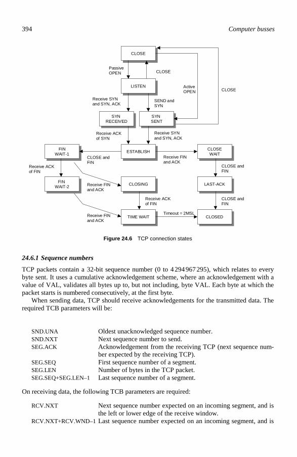
394 Computer busses
CLOSECLOSE
LISTENLISTEN
ESTABLISHESTABLISHFINWAIT-1FIN
WAIT-1CLOSEWAIT
CLOSEWAIT
CLOSINGCLOSINGFIN WAIT-2FIN
WAIT-2 LAST-ACKLAST-ACK
SYN RECEIVED
SYN RECEIVED
SYN SENTSYN SENT
PassiveOPEN CLOSE
SEND andSYN
Receive SYNand SYN, ACK
Receive SYNand SYN, ACK
Receive ACKof SYN
ActiveOPEN CLOSE
CLOSE andFIN
Receive FINand ACK
Receive ACKof FIN
CLOSE andFIN
Receive FINand ACK
TIME WAITTIME WAIT
Receive ACKof FIN
CLOSEDCLOSED
CLOSE andFIN
Receive FINand ACK
Timeout = 2MSL
Figure 24.6 TCP connection states
24.6.1 Sequence numbers
TCP packets contain a 32-bit sequence number (0 to 4 294 967 295), which relates to every byte sent. It uses a cumulative acknowledgement scheme, where an acknowledgement with a value of VAL, validates all bytes up to, but not including, byte VAL. Each byte at which the packet starts is numbered consecutively, at the first byte. When sending data, TCP should receive acknowledgements for the transmitted data. The required TCB parameters will be:
SND.UNA Oldest unacknowledged sequence number. SND.NXT Next sequence number to send. SEG.ACK Acknowledgement from the receiving TCP (next sequence num-
ber expected by the receiving TCP). SEG.SEQ First sequence number of a segment. SEG.LEN Number of bytes in the TCP packet. SEG.SEQ+SEG.LEN–1 Last sequence number of a segment.
On receiving data, the following TCB parameters are required:
RCV.NXT Next sequence number expected on an incoming segment, and is the left or lower edge of the receive window.
RCV.NXT+RCV.WND–1 Last sequence number expected on an incoming segment, and is

TCP and UDP 395
the right or upper edge of the receive window. SEG.SEQ First sequence number occupied by the incoming segment. SEG.SEQ+SEG.LEN–1 Last sequence number occupied by the incoming segment.
24.6.2 ISN selection
The initial sequence number (ISN) is selected so that previous sockets are not confused with new sockets. Typically, this can happen when a host application crashes and then quickly re-establishes the connection before the other side can time-out the connection. To avoid this a 32-bit initial sequence number (ISN) generator is created when the connection is made. The number is generated by a 32-bit clock, which is incremented approximately every 4µs (giv-ing an ISN cycle of 4.55 hours). Thus, within 4.55 hours, each ISN will be unique. As each connection has a send and receive sequence number, these are an initial send sequence number (ISS) and an initial receive sequence number (IRS). When establishing a connection, the two TCPs synchronise their initial sequence numbers. This is done by ex-changing connection establishing packets, with the SYN bit set and with the initial sequence numbers (these packets are typically called SYNs). Thus four packets must be initially ex-changed: • A sends to B. SYN with ASEQ. • B sends to A. ACK of the sequence number (ASEQ). • B sends to A. SYN with BSEQ. • A sends to B. ACK of the sequence number (BSEQ). Note that the two intermediate steps can be combined into a single message. This is some-times knows as a three-way handshake. This handshake is necessary as the sequence num-bers are not tied to a global clock, only to local clocks, and has many advantages, including the fact that old packets will be discarded as they occurred in a previous time. To make sure that a sequence number is not duplicated, a host must wait for a maximum segment lifetime (MSL) before starting to retransmit packets (segments) after start-up or when recovering from a crash. An example MSL is 2 minutes. However, if it is recovering, and it has a memory of the previous sequence numbers, it may not need to wait for the MSL, as it can use sequence numbers which are much greater than the previously used sequence numbers.
24.7 Opening and closing a connection
Figure 24.7 shows a basic three-way handshake. The steps are: 1. The initial state on the initiator is CLOSED and, on the recipient, it is LISTEN (the re-
cipient is waiting for a connection see figure 24.7). 2. The initiator goes into the SYN-SENT state and sends a packet with the SYN bit set and
then indicates that the starting sequence number will be 999 (the current sequence num-ber, thus the next number sent will be 1000). When this is received the recipient goes into the SYN-RECEIVED state.
3. The recipient sends back a TCP packet with the SYN and ACK bits set (which identifies that it is a SYN packet and also that it is acknowledging the previous SYN packet). In

396 Computer busses
this case, the recipient tells the originator that it will start transmitting at a sequence number of 100. The acknowledgement number is 1000, which is the sequence number that the recipient expects to receive next. When this is received, the originator goes into the ESTABLISHED state.
4. The originator sends back a TCP packet with the SYN and ACK bits set and the ac-knowledgement number is 101, which is the sequence number it expects to see next.
5. The originator transmits data with the sequence number of 1000. Originator Recipient 1. CLOSED LISTEN 2. SYN-SENT → <SEQ=999><CTL=SYN> SYN-RECEIVED 3. ESTABLISHED <SEQ=100><ACK=1000> <CTL=SYN,ACK> ← SYN-RECEIVED 4. ESTABLISHED → <SEQ=1000><ACK=101> <CTL=ACK> ESTABLISHED 5. ESTABLISHED → <SEQ=1000><ACK=101> <CTL=ACK><DATA> ESTABLISHED
Figure 24.7 TCP connection
Note that the acknowledgement number acknowledges every sequence number up to but not including the acknowledgement number. Figure 24.8 shows how the three-way handshake prevents old duplicate connection initia-tions from causing confusion. In state 3, a duplicate SYN has been received, which is from a previous connection. The recipient sends back an acknowledgement for this (4), but when this is received by the originator, the originator sends back a RST (reset) packet. This causes the recipient to go back into a LISTEN state. It will then receive the SYN packet sent in 2, and after acknowledging it, a connection is made. TCP connections are half-open if one of the TCPs has closed or aborted, and the other end is still connected. They can also occur if the two connections have become desynchro-nised because of a system crash. This connection is automatically reset if data is sent in ei-ther direction. This is because the sequence numbers will be incorrect, otherwise the connec-tion will time-out. A connection is normally closed with the CLOSE call. A host who has closed cannot continue to send, but can continue to RECEIVE until it is told to close by the other side. Fig-ure 24.9 shows a typical sequence for closing a connection. Normally the application pro-gram sends a CLOSE call for the given connection. Next, a TCP packet is sent with the FIN bit set, the originator enters into the FIN-WAIT-1 state. When the other TCP has acknowl-edged the FIN and sent a FIN of its own, the first TCP can ACK this FIN. Originator Recipient 1. CLOSED LISTEN 2. SYN-SENT → <SEQ=999><CTL=SYN> 3. (duplicate) → <SEQ=900><CTL=SYN> 4. SYN-SENT <SEQ=100><ACK=901> <CTL=SYN,ACK> ← SYN-RECEIVED 5. SYN-SENT → <SEQ=901><CTL=RST> LISTEN 6. (packet 2 received) → 7. SYN-SENT <SEQ=100><ACK=1000><CTL=SYN,ACK> ← SYN-RECEIVED 8. ESTABLISHED → <SEQ=1000><ACK=101><CTL=ACK><DATA> ESTABLISHED
Figure 24.8 TCP connection with duplicate connections

TCP and UDP 397
Originator Recipient 1. ESTABLISHED ESTABLISHED (CLOSE call) 2. FIN-WAIT-1 → <SEQ=1000><ACK=99> <CTL=SFIN,ACK> CLOSE-WAIT 3. FIN-WAIT-2 <SEQ=99><ACK=1001> <CTL=ACK> ← CLOSE-WAIT 4. TIME-WAIT <SEQ=99><ACK=101><CTL=FIN,ACK> ← LAST-ACK 5. TIME-WAIT → <SEQ=1001><ACK=102><CTL=ACK> CLOSED
Figure 24.9 TCP close connection
24.8 TCP user commands
The commands in this section characterise the interface between TCP and the application program. Their actual implementation depends on the operating system. Section 24.9 dis-cusses the WinSock implementation.
24.8.1 OPEN
The OPEN call initiates an active or a passive TCP connection. The basic parameters passed and returned from the call are given next. Parameters in brackets are optional.
Parameters passed: local port, foreign socket, active/passive [, timeout] [, precedence] [, security/compartment] [, options]) Parameters returned: local connection name
These parameters are defined as: • Local port – the local port to be used. • Foreign socket – the definition of the foreign socket. • Active/passive – a passive flag causes TCP to LISTEN, else it will actively seek a con-
nection. • Timeout – if present, this parameter allows the caller to set up a timeout for all data sub-
mitted to TCP. If the data is not transmitted successfully within the timeout period, the connection is aborted.
• Security/compartment – specifies the security of the connection. • Local connection name – a unique connection name is returned which identifies the
socket.
24.8.2 SEND
The SEND call causes the data in the output buffer to be sent to the indicated connection. Most implementations return immediately from the SEND call, even if the data has not been sent, although some implementations will not return until either there is a timeout or the data has been sent. The basic parameters passed and returned from the call are given next. Pa-rameters in brackets are optional.
Parameters passed: local connection name, buffer address, byte count, PUSH flag, URGENT flag [,timeout]

398 Computer busses
These parameters are defined as: • Local connection name – a unique connection name which identifies the socket. • Buffer address – address of data buffer. • Byte count – number of bytes in the buffer. • PUSH flag – if this flag is set then the data will be transmitted immediately, else the TCP
may wait until it has enough data. • URGENT flag – sets the urgent pointer. • Timeout – sets a new timeout for the connection.
24.8.3 RECEIVE
The RECEIVE call allocates a receiving buffer for the specified connection. Most implemen-tations return immediately from the RECEIVE call, even if the data has not been received, although some implementation will not return until either there is a timeout or the data has been received. The basic parameters passed and returned from the call are given next. Pa-rameters in brackets are optional.
Parameters passed: local connection name, buffer address, byte count Parameters returned: byte count, URGENT flag, PUSH flag
These parameters are defined as: • Local connection name – a unique connection name which identifies the socket. • Buffer address – address of the receive data buffer. • Byte count – number of bytes received in the buffer. • PUSH flag – if this flag is set then the PUSH flag has been set on the received data. • URGENT flag – if this flag is set then the URGENT flag has been set on the received
data.
24.8.4 CLOSE
The CLOSE call closes the connections and releases associated resources. All pending SENDs will be transmitted, but after the CLOSE call has been implemented, no further SENDs can occur. RECEIVEs can occur until the other host has also closed the connection. The basic parameters passed and returned from the call are given next.
Parameters passed: local connection name
24.8.5 STATUS
The STATUS call determines the current status of a connection, typically listing the TCBs. The basic parameters passed and returned from the call are given next.
Parameters passed: local connection name Parameters returned: status data
The returned information should include status information on the following: • local socket, foreign socket, local connection name;
TCP and UDP 399
• receive window, send window, connection state; • number of buffers awaiting acknowledgement, number of buffers pending receipt; • urgent state, precedence, security/compartment; • transmission timeout.
24.8.6 ABORT
The ABORT call causes all pending SENDs and RECEIVEs to be aborted. All TCBs are also removed and a RESET message sent to the other TCP. The basic parameters passed and returned from the call are given next. Parameters in brackets are optional. Parameters passed: local connection name
24.9 WinSock
24.9.1 Introduction
The Windows sockets specification describes a common interface for networked Windows programs. WinSock uses TCP/IP communications and provides for binary and source code compatibility for different network types. The Windows sockets API (WinSock application programming interface or WSA) is a library of functions that implement the socket interface by the Berkley Software distribution of UNIX. WinSock augments the Berkley socket implementation by adding Windows-specific extensions to support the message-driven nature of Windows system. The basic implementation normally involves: • Opening a socket – this allows for multiple connections with multiple hosts. Each socket
has a unique identifier. It normally involves defining the protocol suite, the socket type and the protocol name. The API call used for this is socket().
• Naming a socket – this involves assigning location and identity attributes to a socket. The API call used for this is bind().
• Associate with another socket – this involves either listening for a connection or actively seeking a connection. The API calls used in this are listen(), connect()and ac-cept().
• Send and receive between sockets – the API calls used in this are send(), sendto(), recv() and recvfrom().
• Close the socket – the API calls used in this are close() and shutdown().
24.9.2 Windows sockets
The main WinSock API calls are:
socket() Creates a socket. accept() Accepts a connection on a socket. connect() Establishes a connection to a peer. bind() Associates a local address with a socket. listen() Establishes a socket to listen for incoming connection.

400 Computer busses
send() Sends data on a connected socket. sendto() Sends data on an unconnected socket. recv() Receives data from a connected socket. recvfrom() Receives data from an unconnected socket. shutdown() Disables send or receive operations on a socket. closesocket() Closes a socket.
Figure 24.10 shows the operation of a connection of a client to a server. The server is defined as the computer which waits for a connection, the client is the computer which initially makes contact with the server. On the server the computer initially creates a socket with the socket() function, and this is bound to a name with the bind() function. After this, the server listens for a connection with the listen() function. When the client calls the connect() function the server then accepts the connection with accept(). After this the server and client can send and receive data with the send() or recv() functions. When the data transfer is complete the close-socket() is used to close the socket.
socket()create a socket
bind()give socket a
name
listen()listen for
connections
accept()accept a newconnection
send()/recv()send/receive
data
closesocket()close a socket
socket()create a socket
connect()connect to a socket
send()/recv()send/receive
data
closesocket()close a socket
Server Client
Figure 24.10 WinSock connection
socket()
The socket() function creates a socket. Its syntax is

TCP and UDP 401
SOCKET socket (int af, int type, int protocol)
where af A value of PF_INET specifies the ARPA Internet address format specifica-
tion (others include AF_IPX for SPX/IPX and AF_APPLETALK for Apple-Talk).
type Socket specification, which is typically either SOCK_STREAM or SOCK_DGRAM. The SOCK_STREAM uses TCP and provides a sequenced, reliable, two-way, connection-based stream. SOCK_DGRAM uses UDP and provides for connec-tionless datagrams. This type of connection is not recommended. A third type is SOCK_RAW, for types other than UDP or TCP, such as for ICMP.
protocol Defines the protocol to be used with the socket. If it is zero then the caller does not wish to specify a protocol.
If the socket function succeeds then the return value is a descriptor referencing the new socket. Otherwise, it returns SOCKET_ERROR, and the specific error code can be tested with WSAGetLastError. An example creation of a socket is given next: SOCKET s; s=socket(PF_INET,SOCK_STREAM,0); if (s == INVALID_SOCKET) cout << ″Socket error″
bind()
The bind() function associates a local address with a socket. It is called before the connect or listen function. When a socket is created with socket, it exists in a name space (address family), but it has no name assigned. The bind function gives the socket a local association (host address/port number). Its syntax is: int bind(SOCKET s, const struct sockaddr FAR * addr, int namelen) where s A descriptor identifying an unbound socket. namelen The length of addr. addr The address to assign to the socket. The sockaddr structure is defined as follows: struct sockaddr u_short sa_family; char sa_data[14]; ; In the Internet address family, the sockadd_in structure is used by Windows Sockets to spec-ify a local or remote endpoint address to which to connect a socket. This is the form of the sockaddr structure specific to the Internet address family and can be cast to sockaddr. This

402 Computer busses
structure can be filled with the sockaddr_in structure which has the following form:
struct SOCKADDR_IN short sin_family; unsigned short sin_port; struct in_addr sin_addr; char sin_zero[8];
where
sin_family must be set to AF_INET. sin_port IP port. sin_addr IP address. sin_zero padding to make structure the same size as sockaddr.
If an application does not care what address is assigned to it, it may specify an Internet ad-dress equal to INADDR_ANY, a port equal to 0, or both. An Internet address equal to INADDR_ANY causes any appropriate network interface be used. A port value of 0 causes the Windows sockets implementation to assign a unique port to the application with a value be-tween 1024 and 5000. If no error occurs then it returns a zero value. Otherwise, it returns INVALID_SOCKET, and the specific error code can be tested with WSAGetLastError. If an application needs to bind to an arbitrary port outside of the range 1024 to 5000 then the following outline code can be used:
#include <windows.h> #include <winsock.h> int main(void) SOCKADDR_IN sin;
SOCKET s; s = socket(AF_INET,SOCK_STREAM,0); if (s == INVALID_SOCKET) // Socket failed sin.sin_family = AF_INET; sin.sin_addr.s_addr = 0; sin.sin_port = htons(100); // port=100 if (bind(s, (LPSOCKADDR)&sin, sizeof (sin)) == 0) // Bind failed return(0); The Windows sockets htons function converts an unsigned short (u_short) from host byte order to network byte order.

TCP and UDP 403
connect()
The connect() function establishes a connection with a peer. If the specified socket is un-bound then unique values are assigned to the local association by the system and the socket is marked as bound. Its syntax is
int connect (SOCKET s, const struct sockaddr FAR * name, int namelen)
where
s Descriptor identifying an unconnected socket. name Name of the peer to which the socket is to be connected. namelen Name length.
If no error occurs then it returns a zero value. Otherwise, it returns SOCKET_ERROR, and the specific error code can be tested with WSAGetLastError.
listen()
The listen() function establishes a socket which listens for an incoming connection. The sequence to create and accept a socket is: • socket()– Creates a socket. • listen()– this creates a queue for incoming connections and is typically used by a
server that can have more than one connection at a time. • accept()– these connections are then accepted with accept. The syntax of listen() is
int listen (SOCKET s, int backlog) where
s Describes a bound, unconnected socket. backlog Defines the queue size for the maximum number of pending connections
may grow (typically a maximum of 5).
If no error occurs then it returns a zero value. Otherwise, it returns SOCKET_ERROR, and the specific error code can be tested with WSAGetLastError. #include <windows.h> #include <winsock.h> int main(void) SOCKADDR_IN sin; SOCKET s; s = socket(AF_INET,SOCK_STREAM,0); if (s == INVALID_SOCKET)
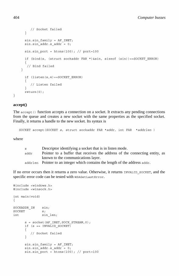
404 Computer busses
// Socket failed sin.sin_family = AF_INET; sin.sin_addr.s_addr = 0; sin.sin_port = htons(100); // port=100 if (bind(s, (struct sockaddr FAR *)&sin, sizeof (sin))==SOCKET_ERROR) // Bind failed if (listen(s,4)==SOCKET_ERROR) // Listen failed return(0);
accept()
The accept() function accepts a connection on a socket. It extracts any pending connections from the queue and creates a new socket with the same properties as the specified socket. Finally, it returns a handle to the new socket. Its syntax is
SOCKET accept(SOCKET s, struct sockaddr FAR *addr, int FAR *addrlen )
where
s Descriptor identifying a socket that is in listen mode. addr Pointer to a buffer that receives the address of the connecting entity, as
known to the communications layer. addrlen Pointer to an integer which contains the length of the address addr.
If no error occurs then it returns a zero value. Otherwise, it returns INVALID_SOCKET, and the specific error code can be tested with WSAGetLastError. #include <windows.h> #include <winsock.h> int main(void) SOCKADDR_IN sin; SOCKET s; int sin_len; s = socket(AF_INET,SOCK_STREAM,0); if (s == INVALID_SOCKET) // Socket failed sin.sin_family = AF_INET; sin.sin_addr.s_addr = 0; sin.sin_port = htons(100); // port=100

TCP and UDP 405
if (bind(s, (struct sockaddr FAR *)&sin, sizeof (sin))==SOCKET_ERROR) // Bind failed if (listen(s,4)<0) // Listen failed sin_len = sizeof(sin); s=accept(s,(struct sockaddr FAR *) & sin,(int FAR *) &sin_len); if (s==INVALID_SOCKET) // Accept failed return(0);
send()
The send() function sends data to a connected socket. Its syntax is:
int send (SOCKET s, const char FAR *buf, int len, int flags)
where
s Connected socket descriptor. buf Transmission data buffer. len Buffer length. flags Calling flag.
The flags parameter influences the behaviour of the function. These can be
MSG_DONTROUTE Specifies that the data should not be subject to routing. MSG_OOB Send out-of-band data.
If send() succeeds then the return value is the number of characters sent (which can be less than the number indicated by len). Otherwise, it returns SOCKET_ERROR, and the specific error code can be tested with WSAGetLastError. #include <windows.h> #include <winsock.h> #include <string.h> #define STRLENGTH 100 int main(void) SOCKADDR_IN sin; SOCKET s; int sin_len; char sendbuf[STRLENGTH]; s = socket(AF_INET,SOCK_STREAM,0); if (s == INVALID_SOCKET)
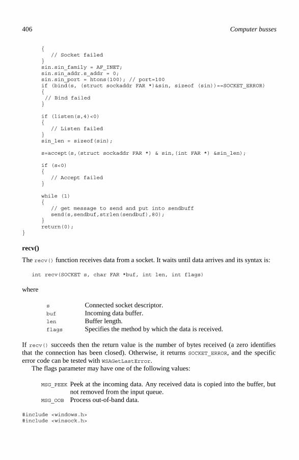
406 Computer busses
// Socket failed sin.sin_family = AF_INET; sin.sin_addr.s_addr = 0; sin.sin_port = htons(100); // port=100 if (bind(s, (struct sockaddr FAR *)&sin, sizeof (sin))==SOCKET_ERROR) // Bind failed if (listen(s,4)<0) // Listen failed sin_len = sizeof(sin); s=accept(s,(struct sockaddr FAR *) & sin,(int FAR *) &sin_len); if (s<0) // Accept failed while (1) // get message to send and put into sendbuff send(s,sendbuf,strlen(sendbuf),80); return(0);
recv()
The recv() function receives data from a socket. It waits until data arrives and its syntax is:
int recv(SOCKET s, char FAR *buf, int len, int flags)
where
s Connected socket descriptor. buf Incoming data buffer. len Buffer length. flags Specifies the method by which the data is received.
If recv() succeeds then the return value is the number of bytes received (a zero identifies that the connection has been closed). Otherwise, it returns SOCKET_ERROR, and the specific error code can be tested with WSAGetLastError. The flags parameter may have one of the following values:
MSG_PEEK Peek at the incoming data. Any received data is copied into the buffer, but not removed from the input queue.
MSG_OOB Process out-of-band data. #include <windows.h> #include <winsock.h>

TCP and UDP 407
#define STRLENGTH 100 int main(void) SOCKADDR_IN sin; SOCKET s; int sin_len,status; char recmsg[STRLENGTH]; s = socket(AF_INET,SOCK_STREAM,0); if (s == INVALID_SOCKET) // Socket failed sin.sin_family = AF_INET; sin.sin_addr.s_addr = 0; sin.sin_port = htons(100); // port=100 if (bind(s, (struct sockaddr FAR *)&sin, sizeof (sin))==SOCKET_ERROR) // Bind failed if (listen(s,4)<0) // Listen failed sin_len = sizeof(sin); s=accept(s,(struct sockaddr FAR *) & sin,(int FAR *) &sin_len); if (s<0) // Accept failed while (1) status=recv(s,recmsg,STRLENGTH,80); if (status==SOCKET_ERROR) // no socket break; recmsg[status]=NULL; // terminate string if (status) // szMsg contains received string else break; // connection broken return(0);

408 Computer busses
shutdown()
The shutdown() function disables send or receive operations on a socket and does not close any opened sockets. Its syntax is
int shutdown(SOCKET s, int how)
where
s Socket descriptor. how Flag that identifies operation types that will no longer be allowed. These are:
0 – Disallows subsequent receives. 1 – Disallows subsequent sends. 2 – Disables send and receive. If no error occurs then it returns a zero value. Otherwise, it returns INVALID_SOCKET, and the specific error code can be tested with WSAGetLastError.
closesocket()
The closesocket() function closes a socket. Its syntax is:
int closesocket (SOCKET s);
where
s Socket descriptor. If no error occurs then it returns a zero value. Otherwise, it returns INVALID_SOCKET, and the specific error code can be tested with WSAGetLastError.
24.10 Visual Basic socket implementation
Visual Basic supports a WinSock control and allows the connection of hosts over a network. It supports both UDP and TCP. Figure 24.11 shows a sample Visual Basic screen with a WinSock object (in this case, it is named Winsock1). To set the protocol used then either select the properties window on the WinSock object, click protocol and select sckTCPProto-col, or sckUDPProtocol. Otherwise, within the code it can be set to TCP with: Winsock1.Protocol = sckTCPProtocol The WinSock object has various properties, such as:
obj.RemoteHost Defines the IP address or domain name of the remote host. obj.LocalPort Defines the local port number.
The methods that are used with the WinSock object are:

TCP and UDP 409
obj.Connect Connects to a remote host (client invoked). obj.Listen Listens for a connection (server invoked). obj.GetData Reads data from the input steam. obj.SendData Sends data to an output stream.
The main events are:
ConnectionRequest Occurs when a remote host wants to make a connection with a server.
DataArrival Occurs when data has arrived from a connection (data is then read with GetData).
Figure 24.11 WinSock object
24.10.1 Creating a server
A server must listen for connection. To do this, do the following: 1 Create a new standard EXE project. 2 Change the name of the default form to myServer. 3 Change the caption of the form to ‘Server Application’ (see Figure 24.12). 4 Put a WinSock control on the main form and change its name to myTCPServer. 5 Add two TextBox controls to the form. Name the first SendTxtData, and the second
ShowText (see Figure 24.12).

410 Computer busses
6 Add the code given below to the form. Private Sub Form_Load() ' Set the local port to 1001 and listen for a connection myTCPServer.LocalPort = 1001 myTCPServer.Listen myClient.Show End Sub Private Sub myTCPServer_ConnectionRequest (ByVal requestID As Long) ' Check state of socket, if it is not closed then close it. If myTCPServer.State <> sckClosed Then myTCPServer.Close ' Accept the request with the requestID parameter. myTCPServer.Accept requestID End Sub Private Sub SendTxtData_Change() ' SendTextData contains the data to be sent. ' This data is setn using the SendData method myTCPServer.SendData = SendTextData.Text End Sub Private Sub myTCPServer_DataArrival (ByVal bytesTotal As Long) ' Read incoming data into the str variable, ' then display it to ShowText Dim str As String myTCPServer.GetData str ShowText.Text = str End Sub
Figure 24.12 Server set-ups
Figure 24.13 shows the server setup.
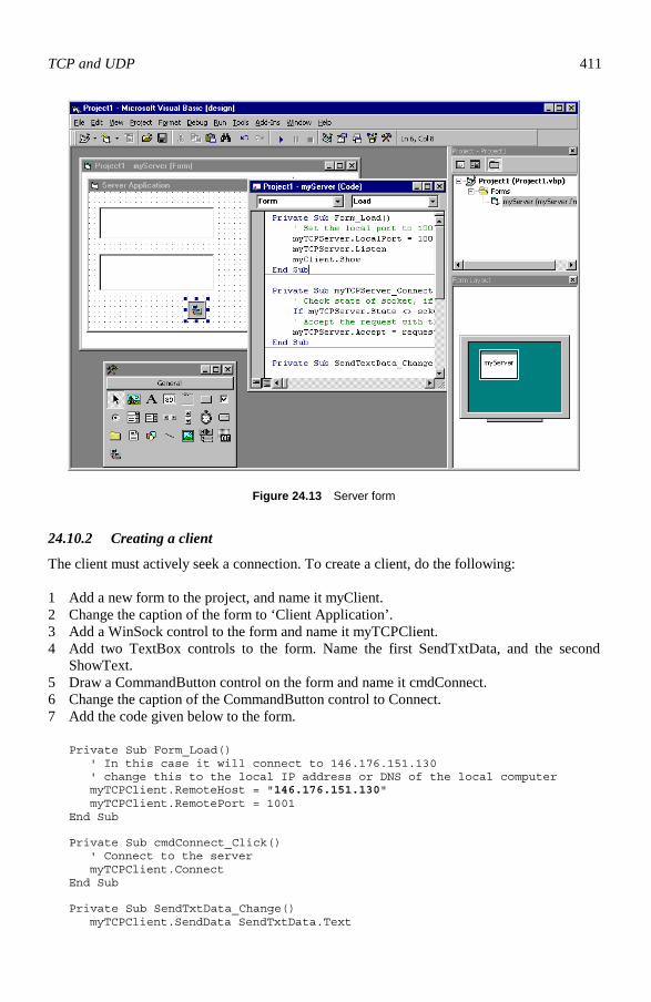
TCP and UDP 411
Figure 24.13 Server form
24.10.2 Creating a client
The client must actively seek a connection. To create a client, do the following: 1 Add a new form to the project, and name it myClient. 2 Change the caption of the form to ‘Client Application’. 3 Add a WinSock control to the form and name it myTCPClient. 4 Add two TextBox controls to the form. Name the first SendTxtData, and the second
ShowText. 5 Draw a CommandButton control on the form and name it cmdConnect. 6 Change the caption of the CommandButton control to Connect. 7 Add the code given below to the form.
Private Sub Form_Load() ' In this case it will connect to 146.176.151.130 ' change this to the local IP address or DNS of the local computer myTCPClient.RemoteHost = "146.176.151.130" myTCPClient.RemotePort = 1001 End Sub Private Sub cmdConnect_Click() ' Connect to the server myTCPClient.Connect End Sub Private Sub SendTxtData_Change() myTCPClient.SendData SendTxtData.Text

412 Computer busses
End Sub Private Sub tcpClient_DataArrival (ByVal bytesTotal As Long) Dim str As String myTCPClient.GetData str ShowText.Text = str End Sub
Figure 24.14 Client form
The program, when it is run, will act as a client and a server. Any text typed in the SendTxtData TextBox will be sent to the ShowText TextBox on the other form.
24.10.3 Multiple connections
In Visual Basic, it is also possible to create multiple connections to a server. This is done by creating multiple occurrences of the server object. A new one is created every time there is a new connection (with the Connection_Request event). Each new server accepts the incoming connection. The following code, which has a WinSock control on a form called multServer, is given below.
Private ConnectNo As Long Private Sub Form_Load() ConnectNo = 0 multServer(0).LocalPort = 1001 multServer(0).Listen End Sub Private Sub multServer_ConnectionRequest _

TCP and UDP 413
(Index As Integer, ByVal requestID As Long) If Index = 0 Then ConnectNo = ConnectNo + 1 Load multServer(ConnectNo) multServer(ConnectNo).LocalPort = 0 multServer(ConnectNo).Accept requestID Load txtData(ConnectNo) End If End Sub
24.10.4 Connect event
The Connect event connects to a server. If an error occurs then a flag (ErrorOccurred) is set to True, else it is False. Its syntax is
Private Sub object.Connect(ErrorOccurred As Boolean)
24.10.5 Close event
The Close event occurs when the remote computer closes the connection. Applications should use the Close method to correctly close their connection. Its syntax is
object_Close()
24.10.6 DataArrival event
The DataArrival event occurs when new data arrives, and returns the number of bytes read (bytesTotal). Its syntax is
object_DataArrival (bytesTotal As Long)
24.10.7 Bind method
The Bind method specifies the local port (LocalPort) and the local IP address (LocalIP) to be used for TCP connections. Its syntax is
object.Bind LocalPort, LocalIP
24.10.8 Listen method
The Listen method creates a socket and goes into listen mode (for server applications). Its stays in this mode until a ConnectionRequest event occurs, which indicates an incoming con-nection. After this, the Accept method should be used to accept the connection. Its syntax is:
object.Listen
24.10.9 Accept method
The Accept method accepts incoming connections after a ConnectionRequest event. Its syn-tax is
object.Accept requestID The requestID parameter is passed into the ConnectionRequest event and is used with the

414 Computer busses
Accept method.
24.10.10 Close method
The Close method closes a TCP connection. Its syntax is
object.Close
24.10.11 SendData method
The SendData methods sends data (Data) to a remote computer. Its syntax is
object.SendData Data
24.10.12 GetData method
The GetData method gets data (Data) from an object. Its syntax is
object.GetData data, [type,] [maxLen]
24.11 Exercises
24.11.1 Which of the following is not part of a TCP header: (a) Host IP address (b) Time-to-live field (c) Host port number (d) Acknowledgement number 24.11.2 Which port does a TELNET server listen to: (a) 21 (b) 25 (c) 25 (d) 80 24.11.3 Which port does an Email server (using SMTP) listen to: (a) 21 (b) 25 (c) 25 (d) 80 24.11.4 Which port does a WWW server (using HTTP) listen to: (a) 21 (b) 25 (c) 25 (d) 80 24.11.5 Which port does an FTP server listen to: (a) 21 (b) 25 (c) 25 (d) 80 24.11.6 What is the main difference between UDP and TCP: (a) TCP uses sequence numbers, makes connections and uses acknowledge-

TCP and UDP 415
ments. (b) They use different addressing schemes. (c) They use different port allocations. (d) UDP only supports one-way traffic, while TCP supports multiplexed traf-
fic. 24.11.7 What is the main method that TCP uses to create a reliable connection: (a) Enhanced error correction (b) Specially coded data (c) Encrypted data (d) Sequence numbers and acknowledgements 24.11.8 How is the initial sequence number of a TCP packet generated: (a) Randomly (b) From a 32-bit clock which is updated every 4 µs (c) From a universal Internet-based clock (d) From the system clock 24.11.9 How many packets are exchanged in setting up an established TCP connection: (a) 1 (b) 2 (c) 3 (d) 4 24.11.10 Outline the operation of the three-way handshaking. 24.11.11 What advantages does TCP have over UDP. Investigate server applications which
use UDP. 24.11.12 If possible, implement a basic client/server application with either C++ or Visual
Basic. As a test, run the client and the server on the same computer. (Note the IP address of the computer as this is required by the client.)
24.11.13 Change the program in Exercise 24.11.12 so that the client and the server run on
different computers (note the IP address of the server as this is required by the cli-ent). If possible, run the program on different network segments.
For the following questions, download a program from the WWW which connects
to a specified port on a specified server. 24.11.14 Connect to a WWW server using port 13. This port should return the current date
and time. 24.11.15 Connect to a WWW server using port 19. 24.11.16 Connect two computers over a network and set up a chat connection. One of the
computers should be the chat server and the other the chat client. Modify it so that the server accepts calls from one or many clients.

416 Computer busses
24.12 TCP/IP services reference
Port Service Comment Port Service Comment 1 TCPmux 7 echo 9 discard Null 11 systat Users 13 daytime 15 netstat 17 qotd Quote 18 msp Message send protocol 19 chargen ttytst source 21 ftp 23 telnet 25 smtp Mail 37 time Timserver 39 rlp Resource location 42 nameserver IEN 116 43 whois Nicname 53 domain DNS 57 mtp Deprecated 67 bootps BOOTP server 67 bootps 68 bootpc BOOTP client 69 tftp 70 gopher Internet Gopher 77 rje Netrjs 79 finger 80 www WWW HTTP 87 link Ttylink 88 kerberos Kerberos v5 95 supdup 101 hostnames 102 iso-tsap ISODE 105 csnet-ns CSO name server 107 rtelnet Remote Telnet 109 pop2 POP version 2 110 pop3 POP version 3 111 sunrpc 113 auth Rap ID 115 sftp 117 uucp-path 119 nntp USENET 123 ntp Network Timel 137 netbios-ns NETBIOS name service 138 netbios-dgm NETBIOS 139 netbios-ssn NETBIOS session 143 imap2 161 snmp SNMP 162 snmp-trap SNMP trap 163 cmip-man ISO management over IP 164 cmip-agent 177 xdmcp X display manager 178 nextstep NeXTStep 179 bgp BGP 191 prospero 194 irc Internet relay chat 199 smux SNMP multiplexor 201 at-rtmp AppleTalk routing 202 at-nbp AppleTalk name binding 204 at-echo AppleTalk echo 206 at-zis AppleTalk zone information 210 z3950 NISO Z39.50 database 213 ipx IPX 220 imap3 Interactive mail access 372 ulistserv UNIX Listserv 512 exec Comsat 513 login 513 who Whod 514 shell No passwords used 514 syslog 515 printer Line printer spooler 517 talk 518 ntalk 520 route RIP 525 timed Timeserver 526 tempo Newdate 530 courier Rpc 531 conference Chat 532 netnews Readnews 533 netwall Emergency broadcasts 540 uucp Uucp daemon 543 klogin Kerberized ‘rlogin’ (v5) 544 kshell Kerberized ‘rsh’ (v5)
24.13 Notes from the author
In this chapter I have presented the two opposite ends of code development for TCP/IP com-munications. The C++ code is complex, but very powerful, and allows for a great deal of flexibility. On the other hand, the Visual Basic code is simple to implement but is difficult to

TCP and UDP 417
implement for non-typical applications. Thus, the code used tends to reflect the type of appli-cation. In many cases Visual Basic gives an easy-to-implement package, with the required functionality. I’ve seen many a student wilt at the prospect of implementing a Microsoft Win-dows program in C++. ‘Where do I start’, is always the first comment, and then ‘How do I do text input’, and so on. Visual Basic, on the other hand, has matured into an excellent de-velopment system which hides much of the complexity of Microsoft Windows away from the developer. So, don’t worry about computer language snobbery. Pick the best language to implement the specification. UDP transmission can be likened to sending electronic mail. In most electronic mail packages the user can request that a receipt is sent back to the originator when the elec-tronic mail has been opened. This is equivalent to TCP, where data is acknowledged after a certain amount of data has been sent. If the user does not receive a receipt for their elec-tronic mail then they will send another one, until it is receipted or until there is a reply. UDP is equivalent to a user sending an electronic mail without asking for a receipt, thus the origi-nator has no idea if the data has been received, or not. TCP/IP is an excellent method for networked communications, as IP provides the routing of the data, and TCP allows acknowledgements for the data. Thus, the data can always be guaranteed to be correct. Unfortunately there is an overhead in the connection of the TCP socket, where the two communicating stations must exchange parameters before the connec-tion is made, then they must maintain and acknowledge received TCP packets. UDP has the advantage that it is connectionless. So there is no need for a connection to be made, and data is simply thrown in the network, without the requirement for acknowledgments. Thus UDP packets are much less reliable in their operation, and a sending station cannot guarantee that the data is going to be received. UDP is thus useful for remote data acquisition where data can be simply transmitted without it being requested or without a TCP/IP connection being made. The concept of ports and sockets is important in TCP/IP. Servers wait and listen on a given port number. They only read packets which have the correct port number. For exam-ple, a WWW server listens for data on port 80, and an FTP server listens for port 21. Thus a properly set up communication network requires a knowledge of the ports which are ac-cessed. An excellent method for virus writers and hackers to get into a network is to install a program which responds to a given port which the hacker uses to connect to. Once into the system they can do a great deal of damage. Programming languages such as Java have built-in security to reduce this problem.

Interrupt-driven RS-232
28.1 Interrupt-driven RS-232
Interrupt-driven devices are efficient on processor time as they allow the processor to run a program without having to poll the devices. This allows fast devices almost instant access to the processor and stops slow devices from ‘hogging’ the processor. For example, a line printer tends to be slow in printing characters. If the printer only interrupted the processor when it was ready for data then the processor can do other things while the printer is printing the character. Another example can be found in serial communications. Characters sent over an RS-232 link are transmitted and received relatively slowly. In a non-interrupt-driven sys-tem the computer must poll the status register to determine if a character has been received, which is inefficient in processor time. But, if the amount of time spent polling the status reg-ister is reduced, there is a possibility of the computer missing the received character as an-other could be sent before the first is read from the receiver buffer. If the serial communica-tions port was set up to interrupt the processor when a new character arrived then it is guar-anteed that the processor will always process the receiver buffer. A major disadvantage with non-interrupt-driven software is when the processor is in-volved in a ‘heavy processing’ task such as graphics or mathematical calculations. This can have the effect of reducing the amount of time that can be spent in polling and/or reading data.
28.2 DOS-based RS-232 program
Program 28.1 is a simple interrupt-driven DOS-based RS-232 program which is written for Turbo/Borland C/C++. If possible, connect two PCs together with a cable which swaps the TX and RX lines, as shown in Figure 13.18. Each of the computers should be able to trans-mit and receive concurrently. A description of this program is given in the next section. The header file associated with this program is serial.h.
Program 28.1 #include <dos.h> #include <conio.h> #include <stdio.h> #include <bios.h> #include "serial.h" void interrupt rs_interrupt(void); void setup_serial(void); void send_character(int ch);
28

480 Computer busses
int get_character(void); int get_buffer(void); void set_vectors(void); void reset_vectors(void); void enable_interrupts(void); void disable_interrupts(void); void interrupt(*oldvect)(); char buffer[RSBUFSIZE]; unsigned int startbuf=0,endbuf = 0; int main(void) int ch, done = FALSE; setup_serial(); set_vectors(); /* set new interrupt vectors and store old ones */ enable_interrupts(); printf("Terminal emulator, press [ESC] to quit\n"); do if (kbhit()) ch=getche(); if (ch==ESC) break; send_character(ch); /* empty RS232 buffer */ do if ((ch=get_buffer()) != -1) putch(ch); while (ch!=-1); while (!done); disable_interrupts(); reset_vectors(); return(0); void interrupt rs_interrupt(void) disable(); if ((inportb(IIR) & RX_MASK) == RX_ID) buffer[endbuf] = inportb(RXR); endbuf++; if (endbuf == RSBUFSIZE) endbuf=0; /* Set end of interrupt flag */ outportb(ICR, EOI); enable(); void setup_serial(void) int RS232_setting; RS232_setting=BAUD1200 | STOPBIT1 | NOPARITY | DATABITS7; bioscom(0,RS232_setting,COM1); void send_character(int ch)

Interrupt-driven RS-232 481
char status; do status = inportb(LSR) & 0x40; while (status!=0x40); /*repeat until Tx buffer empty ie bit 6 set*/ outportb(TXDATA,(char) ch); int get_character(void) int status; do status = inportb(LSR) & 0x01; while (status!=0x01); /* Repeat until bit 1 in LSR is set */ return( (int)inportb(TXDATA)); int get_buffer(void) int ch; if (startbuf == endbuf) return (-1); ch = (int) buffer[startbuf]; startbuf++; if (startbuf == RSBUFSIZE) startbuf = 0; return (ch); void set_vectors(void) oldvect = getvect(0x0C); setvect(0x0C, rs_interrupt); /* Uninstall interrupt vectors before exiting the program */ void reset_vectors(void) setvect(0x0C, oldvect); void disable_interrupts(void) int ch; disable(); ch = inportb(IMR) | ~IRQ4; /* disable IRQ4 interrupt */ outportb(IMR, ch); outportb(IER, 0); enable(); void enable_interrupts(void) int ch; disable(); /* initialize rs232 port */ ch = inportb(MCR) | MC_INT; outportb(MCR, ch); /* enable interrupts for IRQ4 */ outportb(IER, 0x01); ch = inportb(IMR) & IRQ4;

482 Computer busses
outportb(IMR, ch); enable();
Header file 28.1: serial.h #define FALSE 0 /* RS232 set up parameters */ #define COM1 0 #define COM2 1 #define DATABITS7 0x02 #define DATABITS8 0x03 #define STOPBIT1 0x00 #define STOPBIT2 0x04 #define NOPARITY 0x00 #define ODDPARITY 0x08 #define EVENPARITY 0x18 #define BAUD110 0x00 #define BAUD150 0x20 #define BAUD300 0x40 #define BAUD600 0x60 #define BAUD1200 0x80 #define BAUD2400 0xA0 #define BAUD4800 0xC0 #define BAUD9600 0xE0 #define ESC 0x1B /* ASCII Escape character */ #define RSBUFSIZE 10000 /* RS232 buffer size */ #define COM1BASE 0x3F8 /* Base port address for COM1 */ #define TXDATA COM1BASE /* Transmit register */ #define RXR COM1BASE /* Receive register */ #define IER (COM1BASE+1) /* Interrupt Enable */ #define IIR (COM1BASE+2) /* Interrupt ID */ #define LCR (COM1BASE+3) /* Line control */ #define MCR (COM1BASE+4) /* Line control */ #define LSR (COM1BASE+5) /* Line Status */ #define RX_ID 0x04 #define RX_MASK 0x07 #define MC_INT 0x08 /* Addresses of the 8259 Programmable Interrupt Controller (PIC).*/ #define IMR 0x21 /* Interrupt Mask Register port */ #define ICR 0x20 /* Interrupt Control Port */ /* An end of interrupt needs to be sent to the Control Port of */ /* the 8259 when a hardware interrupt ends. */ #define EOI 0x20 /* End Of Interrupt */ #define IRQ4 0xEF /* COM1 */
28.2.1 Description of program
The initial part of the program sets up the required RS-232 parameters. It uses bioscom() to

Interrupt-driven RS-232 483
set COM1: with the parameters of 1200 bps, 1 stop bit, no parity and 7 data bits. void setup_serial(void) int RS232_setting; RS232_setting=BAUD1200 | STOPBIT1 | NOPARITY | DATABITS7; bioscom(0,RS232_setting,COM1);
After the serial port has been initialized the interrupt service routine for the IRQ4 line is set to point to a new ‘user-defined’ service routine. The primary serial port COM1: sets the IRQ4 line active when it receives a character. The interrupt associated with IRQ4 is 0Ch (12). The get-vect() function gets the ISR address for this interrupt, which is then stored in the variable oldvect so that at the end of the program it can be restored. Finally, in the set_vectors() function, the interrupt assigns a new ‘user-defined’ ISR (in this case it is the function rs_interrupt()). void set_vectors(void) oldvect = getvect(0x0C); /* store IRQ4 interrupt vector */ setvect(0x0C, rs_interrupt); /* set ISR to rs_interrupt() */
At the end of the program the ISR is restored with the following code. void reset_vectors(void) setvect(0x0C, oldvect); /* reset IRQ4 interrupt vector */
The COM1: port is initialized for interrupts with the code given next. The statement ch = inportb ( MCR ) | 0x08;
resets the RS-232 port by setting bit 3 for the modem control register (MCR) to a 1. Some RS-232 ports require this bit to be set. The interrupt enable register (IER) enables interrupts on a port. Its address is offset by 1 from the base address of the port (that is, 0x3F9 for COM1:). If the least significant bit of this register is set to a 1 then interrupts are enabled, else they are disabled. To enable the IRQ4 line on the PIC, bit 5 of the IMR (interrupt mask register) is to be set to a 0 (zero). The statement: ch = inportb(IMR) & 0xEF;
achieves this as it bitwise ANDs all the bits, except for bit 4, with a 1. This is because any bit which is ANDed with a 0 results in a 0. The bit mask 0xEF has been defined with the macro IRQ4. void enable_interrupts(void) int ch; disable(); ch = inportb(MCR) | MC_INT; /* initialize rs232 port */ outportb(MCR, ch); outportb(IER, 0x01); ch = inportb(IMR) & IRQ4;

484 Computer busses
outportb(IMR, ch); /* enable interrupts for IRQ4 */ enable();
At the end of the program the function disable_interrupts() sets the IER register to all 0s. This disables interrupts on the COM1: port. Bit 4 of the IMR is also set to a 1 which disables IRQ4 interrupts. void disable_interrupts(void) int ch; disable(); ch = inportb(IMR) | ~IRQ4; /* disable IRQ4 interrupt */ outportb(IMR, ch); outportb(IER, 0); enable();
The ISR for the IRQ4 function is set to rs_interrupt(). When it is called, the Interrupt Status Register (this is named IIR to avoid confusion with the interrupt service routine) is tested to determine if a character has been received. Its address is offset by 2 from the base address of the port (that is, 0x3FA for COM1:). The first 3 bits give the status of the interrupt. A 000b indicates that there are no interrupts pending, a 100b that data has been received, or a 111b that an error or break has occurred. The statement if ((inportb(IIR) & 0x7) == 0x4) tests if data has been received. If this statement is true then data has been received and the character is then read from the receiver buffer array with the statement buffer[endbuf] = inportb(RXR);. The end of the buffer variable (endbuf) is then incremented by 1. At the end of this ISR the end of interrupt flag is set in the interrupt control register with the statement outportb(ICR, 0x20);. The startbuf and endbuf variables are global, thus all parts of the program have access to them. Turbo/Borland functions enable() and disable() in rs_interrupt() are used to enable and disable interrupts, respectively. void interrupt rs_interrupt(void) disable(); if ((inportb(IIR) & RX_MASK) == RX_ID) buffer[endbuf] = inportb(RXR); endbuf++; if (endbuf == RSBUFSIZE) endbuf=0; /* Set end of interrupt flag */ outportb(ICR, EOI); enable();
The get_buffer() function is given next. It is called from the main program and it tests the variables startbuf and endbuf. If they are equal then it returns –1 to the main(). This indi-cates that there are no characters in the buffer. If there are characters in the buffer then the function returns, the character pointed to by the startbuf variable. This variable is then in-cremented. The difference between startbuf and endbuf gives the number of characters in the buffer. Note that when startbuf or endbuf reach the end of the buffer (RSBUFSIZE) they are set back to the first character, that is, element 0.

Interrupt-driven RS-232 485
int get_buffer(void) int ch; if (startbuf == endbuf) return (-1); ch = (int) buffer[startbuf]; startbuf++; if (startbuf == RSBUFSIZE) startbuf = 0; return (ch);
The get_character() and send_character() functions are similar to those developed in Chapter 13. For completeness, these are listed next. void send_character(int ch) char status; do status = inportb(LSR) & 0x40; while (status!=0x40); /*repeat until Tx buffer empty ie bit 6 set*/ outportb(TXDATA,(char) ch); int get_character(void) int status; do status = inportb(LSR) & 0x01; while (status!=0x01); /* Repeat until bit 1 in LSR is set */ return( (int)inportb(TXDATA));
The main() function calls the initialization and the de-initialization functions. It also contains a loop, which continues until the Esc key is pressed. Within this loop, the keyboard is tested to determine if a key has been pressed. If it has then the getche() function is called. This function returns a key from the keyboard and displays it to the screen. Once read into the variable ch it is tested to determine if it is the Esc key. If it is then the program exits the loop, else it transmits the entered character using the send_character() function. Next the get_buffer() function is called. If there are no characters in the buffer then a –1 value is returned, else the character at the start of the buffer is returned and displayed to the screen using putch(). int main(void) int ch, done = FALSE; setup_serial(); /* set new interrupt vectors and store old ones */ set_vectors(); enable_interrupts(); printf("Terminal emulator, press [ESC] to quit\n"); do

486 Computer busses
if (kbhit()) ch=getche(); if (ch==ESC) break; send_character(ch); /* empty RS232 buffer */ do if ((ch=get_buffer()) != -1) putch(ch); while (ch!=-1); while (!done); disable_interrupts(); reset_vectors(); return(0);
28.3 Exercises
28.3.1 Modify Program 28.1 so that a new-line character is displayed properly. 28.3.2 Prove that Program 28.1 is a true multitasking system by inserting a delay in the
main loop, as shown next. The program should be able to buffer all received char-acters and display them to the screen when the sleep delay is over.
do sleep(10); /* go to sleep for 10 seconds, real-time system */ /* will buffer all received characters */ if (kbhit()) ch=getche(); if (ch==ESC) break; send_character(ch); /* empty RS232 buffer */ do if ((ch=get_buffer()) != -1) putch(ch); while (ch!=-1); while (!done);
28.3.3 Modify Program 28.1 so that the transmitted characters are displayed in the top
half of the screen and then received in the bottom half of the screen. 28.3.4 Modify Program 28.1 so that it communicates via COM2: (if the PC has one). 28.3.5 Using a loopback connection on a serial port, write a program, which sends out the
complete ASCII table and checks it against the received characters. 28.3.6 Outline how a program could communicate with a serial port card with eight serial

Interrupt-driven RS-232 487
lines on it. Normally the IRQ lines for COM3 to COM8 can set to either IRQ3 to IRQ4 with jumpers on the board. Investigate typical base addresses for COM3 to COM8. Thus explain how multiple devices can be connected to a single interrupt line.
28.3.7 Implement a program which has a write buffer system. This should fill a buffer
with characters and only send them once every 30 seconds. Modify the program so that the user can enter the delay time.
28.3.8 Write a program which sends the complete contents of a text file from one com-
puter to another. The receiving program should wait for the sending program to send the file and the sending program should prompt the user on the name of the file. The sending program must thus identify the name of the file to the receiver. A typical protocol could be:
1. Send name of the file followed by an invalid file name character, such as: myfile.txt*
which would identify that the name of the file to be sent is myfile.txt. 2. Send each of the characters in the file one by one. The end of the file is then identified by the end-of-file (EOF) character. 28.3.9 Modify the program in Exercise 28.3.8 so that a binary file can be sent. Note that
in a binary file the EOF character can occur at a point in the file. There are two possible methods which can be used to implement this. These are:
• Implement a time-out on the characters received. When no characters have
been received after, say, 1 second then it is assumed that the EOF has oc-curred. The receiver will then close the file.
• The sender sends some initial information on the filename, number of bytes in
the file, date and time, and so on. This could be a fixed format header.
• Send a second EOF character whenever there is an EOF character which is not the EOF marker. Thus when the receiver receives two consecutive EOF char-acters, it simply deletes one of them. When it receives a single EOF character (within a given time) then it knows it is at the end of the file.
28.3.10 Modify the program in Exercise 28.3.9 so that a user on the receiving computer
can specify the filename which is to be sent from the sending program.

PC Processors
A.1 Introduction
Intel marketed the first microprocessor, named the 4004. This device caused a revolution in the electronics industry because previous electronic systems had a fixed functionality. With this processor the functionality could be programmed by software. It could handle four bits of data at a time (a nibble), contained 2000 transistors, had 46 instructions and allowed 4 KB of program code and 1 KB of data. The PC has since evolved using Intel microprocessors (Intel is a contraction of Integrated Electronics). The second generation of Intel microprocessors began in 1974. These could handle 8 bits (a byte) of data at a time and were named the 8008, 8080 and the 8085. They were much more powerful than the previous 4-bit devices and were used in many early microcomputers and applications such as electronic instruments and printers. The 8008 has a 14-bit address bus and can thus address up to 16 kB of memory (the 8080 has a 16-bit address bus giving it a 64 kB limit). The third generation of microprocessors began with the launch of the 16-bit processors. Intel released the 8086 microprocessor which was mainly an extension to the original 8080 processor and thus retained a degree of software compatibility. IBM’s designers realised the power of the 8086 and used it in the original IBM PC and IBM XT (eXtended Technology). It has a 16-bit data bus and a 20-bit address bus, and thus has a maximum addressable capac-ity of 1 MB. A stripped-down 8-bit external data bus version called the 8088 is also available. This stripped down processor allowed designers to produce less complex (and cheaper) computer systems. The 8086 could handle either 8 or 16 bits of data at a time (although in a messy way). An improved architecture version, called the 80286, was launched in 1982, and was used in the IBM AT (Advanced Technology). In 1985, Intel introduced its first 32-bit microprocessor, the 80386DX. This device was compatible with the previous 8088/8086/80286 (80X86) processors and gave excellent per-formance handling 8, 16 or 32 bits at a time. It has full 32-bit data and address buses and can thus address up to 4 GB of physical memory. A stripped-down 16-bit external data bus and 24-bit address bus version called the 80386SX was released in 1988. This processor can thus only access up to 16 MB of physical memory. In 1989, Intel introduced the 80486DX which is basically an improved 80386DX with a memory cache and math co-processor integrated onto the chip. It had an improved internal structure making it around 50% faster than a comparable 80386. The 80486SX was also in-troduced, which is merely a 80486DX with the link to the math co-processor broken. Clock doubler/ trebler 80486 processors were also released. In these devices the processor runs at a higher speed than the system clock. Typically, systems with clock doubler processors are around 75% faster than the comparable non-doubled processors. Typical clock doubler proc-essors are DX2-66 and DX2-50 which run from 33 MHz and 25 MHz clocks, respectively. Intel also produced a new range of microprocessors which run at three or four times the sys-
A
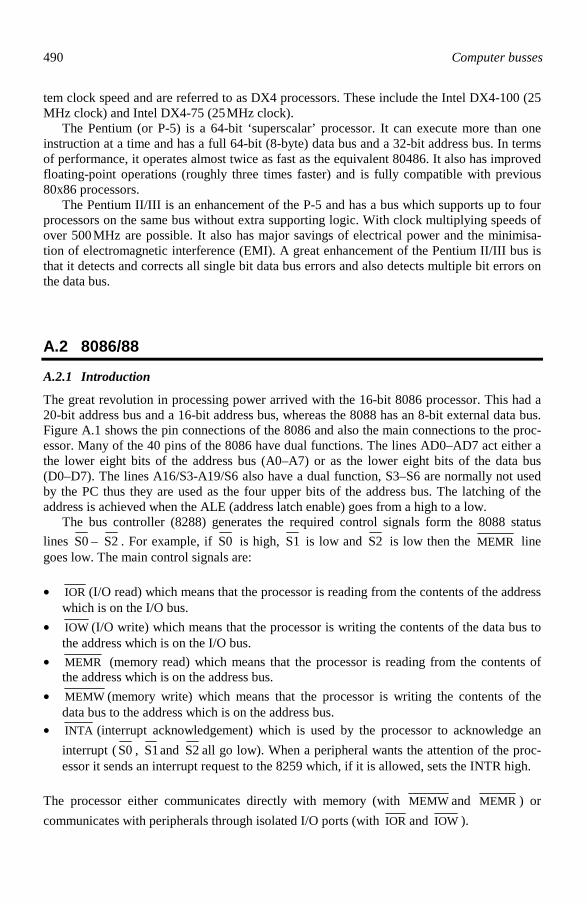
490 Computer busses
tem clock speed and are referred to as DX4 processors. These include the Intel DX4-100 (25 MHz clock) and Intel DX4-75 (25 MHz clock). The Pentium (or P-5) is a 64-bit ‘superscalar’ processor. It can execute more than one instruction at a time and has a full 64-bit (8-byte) data bus and a 32-bit address bus. In terms of performance, it operates almost twice as fast as the equivalent 80486. It also has improved floating-point operations (roughly three times faster) and is fully compatible with previous 80x86 processors. The Pentium II/III is an enhancement of the P-5 and has a bus which supports up to four processors on the same bus without extra supporting logic. With clock multiplying speeds of over 500 MHz are possible. It also has major savings of electrical power and the minimisa-tion of electromagnetic interference (EMI). A great enhancement of the Pentium II/III bus is that it detects and corrects all single bit data bus errors and also detects multiple bit errors on the data bus.
A.2 8086/88
A.2.1 Introduction
The great revolution in processing power arrived with the 16-bit 8086 processor. This had a 20-bit address bus and a 16-bit address bus, whereas the 8088 has an 8-bit external data bus. Figure A.1 shows the pin connections of the 8086 and also the main connections to the proc-essor. Many of the 40 pins of the 8086 have dual functions. The lines AD0–AD7 act either a the lower eight bits of the address bus (A0–A7) or as the lower eight bits of the data bus (D0–D7). The lines A16/S3-A19/S6 also have a dual function, S3–S6 are normally not used by the PC thus they are used as the four upper bits of the address bus. The latching of the address is achieved when the ALE (address latch enable) goes from a high to a low. The bus controller (8288) generates the required control signals form the 8088 status lines S0 – S2 . For example, if S0 is high, S1 is low and S2 is low then the MEMR line goes low. The main control signals are: • IOR (I/O read) which means that the processor is reading from the contents of the address
which is on the I/O bus. • IOW (I/O write) which means that the processor is writing the contents of the data bus to
the address which is on the I/O bus. • MEMR (memory read) which means that the processor is reading from the contents of
the address which is on the address bus. • MEMW (memory write) which means that the processor is writing the contents of the
data bus to the address which is on the address bus. • INTA (interrupt acknowledgement) which is used by the processor to acknowledge an
interrupt ( S0 , S1and S2 all go low). When a peripheral wants the attention of the proc-essor it sends an interrupt request to the 8259 which, if it is allowed, sets the INTR high.
The processor either communicates directly with memory (with MEMW and MEMR ) or communicates with peripherals through isolated I/O ports (with IOR and IOW ).
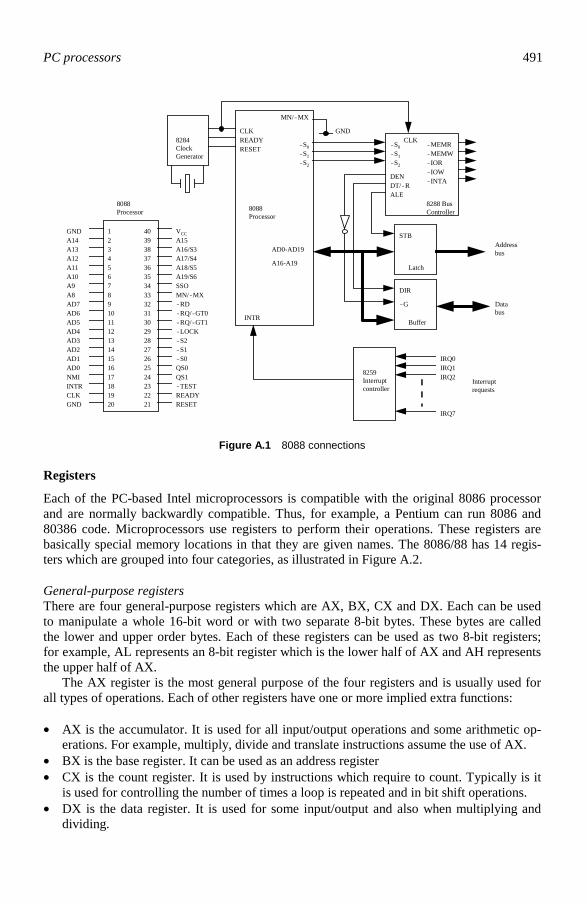
PC processors 491
-S0-S1-S2
-S0-S1-S2
MN/-MX
-MEMR-MEMW-IOR-IOW-INTA
DENDT/-RALE
CLKREADYRESET
AD0-AD19
A16-A19
STB
DIR
-G
8288 Bus Controller8088
Processor
8284Clock Generator
CLK
40 VCC39
A16/S338A17/S437A18/S536A19/S635SSO34MN/-MX33-RD32-RQ/-GT031-RQ/-GT130-LOCK29-S228-S127-S026QS025QS124-TEST23READY22RESET
12345678910111213141516171819
2120
A15GND
A13A12A11A10A9A8AD7AD6AD5AD4AD3AD2AD1AD0NMIINTRCLKGND
A14
8088Processor
Addressbus
Databus
GND
Buffer
Latch
8259Interruptcontroller
INTR
IRQ0IRQ1IRQ2
IRQ7
Interruptrequests
Figure A.1 8088 connections
Registers
Each of the PC-based Intel microprocessors is compatible with the original 8086 processor and are normally backwardly compatible. Thus, for example, a Pentium can run 8086 and 80386 code. Microprocessors use registers to perform their operations. These registers are basically special memory locations in that they are given names. The 8086/88 has 14 regis-ters which are grouped into four categories, as illustrated in Figure A.2.
General-purpose registers There are four general-purpose registers which are AX, BX, CX and DX. Each can be used to manipulate a whole 16-bit word or with two separate 8-bit bytes. These bytes are called the lower and upper order bytes. Each of these registers can be used as two 8-bit registers; for example, AL represents an 8-bit register which is the lower half of AX and AH represents the upper half of AX. The AX register is the most general purpose of the four registers and is usually used for all types of operations. Each of other registers have one or more implied extra functions: • AX is the accumulator. It is used for all input/output operations and some arithmetic op-
erations. For example, multiply, divide and translate instructions assume the use of AX. • BX is the base register. It can be used as an address register • CX is the count register. It is used by instructions which require to count. Typically is it
is used for controlling the number of times a loop is repeated and in bit shift operations. • DX is the data register. It is used for some input/output and also when multiplying and
dividing.

492 Computer busses
AX (Accumulator)
BX (Base register)
CX (Count register)
DX (Data register)
SP (Stack pointer)
BP (Base pointer)
SP (Source pointer)
DI (Destination index)
CS (Code segment)
DS (Data segment)
SS (Stack segment)
AH AL
8 bits 8 bits
BH BL
8 bits 8 bits
CH CL
8 bits 8 bits
DH DL
8 bits 8 bits
* * * * O D I T S Z * A * P * C
Flags
Figure A.2 8086/88 registers
Addressing registers The addressing registers are used in memory addressing operations, such as the holding the source address of the memory and the destination address. These address registers are named BP, SP, SI and DI, which are: • SI is the source index. This is used with extended addressing commands. • DI is the destination index. The destination is used in some addressing modes. • BP is the base pointer. • SP is the stack pointer.
Status registers Status registers are used to test for various conditions in an operation, such as ‘is the result negative’, ‘is the result zero’, and so on. The two status registers have 16 bits and are called the instruction pointer (IP) and the flag register (F): • IP is the instruction pointer. The IP register contains the address of the next instruction of
the program. • Flag register. The flag register holds a collection of 16 different conditions. Table A.1
outlines the most-used flags.
Segments registers There are four areas of memory called segments, each of which are 16 bits and can thus ad-dress up to 64 KB (from 0000h to FFFFh). These segments are: • Code segment (CS register) – defines the memory location where the program code (or

PC processors 493
instructions) is stored. • Data segment (DS register) – defines where data from the program will be stored (DS
stands for data segment register). • Stack segment (SS register) – defines where the stack is stored. • Extra segment (ES). All addresses are with reference to the segment registers. The 8086 has a segmented memory, these registers are used to manipulate these seg-ments. Each segment provides 64 K of memory, this area of memory is known as the current segment.
Table A.1 Processor flags
Bit Flag position
Name Description
C 0 Set on carry Contains the carry from the most significant bit (left hand bit) following a shift, rotate or arithmetic op-eration.
A 4 Set on 1/2 carry
S 7 Set on negative result Contains the sign of an arithmetic operation (0 for positive, 1 for negative).
Z 6 Set on zero result
Contains results of last arithmetic or compare result (0 for nonzero, 1 for zero).
O 11 Set on overflow Indicates that an overflow has occurred in the most significant bit from an arithmetic operation.
P 2 Set on even parity
D 10 Direction
I 9 Interrupt enable Indicates whether the interrupt has been disabled.
T 8 Trap
Memory Addressing There are several methods of accessing memory locations, these are: • Implied addressing which uses an instruction in which it is known the which registers are
used. • Immediate (or literal) addressing uses a simple constant number to define the address
location. • Register addressing which uses the address registers for the addressing (such as AX, BX ,
and so on). • Memory addressing which is used to read or write to a specified memory location.
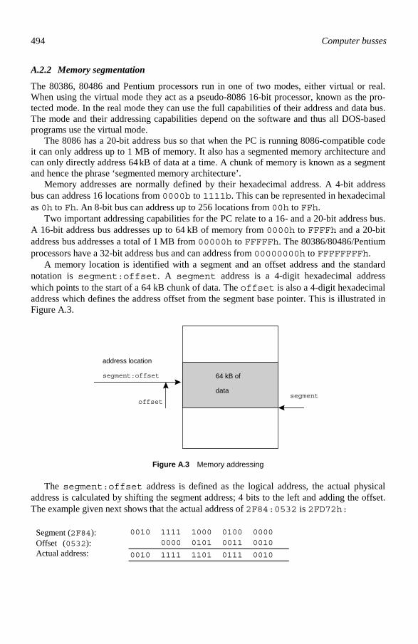
494 Computer busses
A.2.2 Memory segmentation
The 80386, 80486 and Pentium processors run in one of two modes, either virtual or real. When using the virtual mode they act as a pseudo-8086 16-bit processor, known as the pro-tected mode. In the real mode they can use the full capabilities of their address and data bus. The mode and their addressing capabilities depend on the software and thus all DOS-based programs use the virtual mode. The 8086 has a 20-bit address bus so that when the PC is running 8086-compatible code it can only address up to 1 MB of memory. It also has a segmented memory architecture and can only directly address 64 kB of data at a time. A chunk of memory is known as a segment and hence the phrase ‘segmented memory architecture’. Memory addresses are normally defined by their hexadecimal address. A 4-bit address bus can address 16 locations from 0000b to 1111b. This can be represented in hexadecimal as 0h to Fh. An 8-bit bus can address up to 256 locations from 00h to FFh. Two important addressing capabilities for the PC relate to a 16- and a 20-bit address bus. A 16-bit address bus addresses up to 64 kB of memory from 0000h to FFFFh and a 20-bit address bus addresses a total of 1 MB from 00000h to FFFFFh. The 80386/80486/Pentium processors have a 32-bit address bus and can address from 00000000h to FFFFFFFFh. A memory location is identified with a segment and an offset address and the standard notation is segment:offset. A segment address is a 4-digit hexadecimal address which points to the start of a 64 kB chunk of data. The offset is also a 4-digit hexadecimal address which defines the address offset from the segment base pointer. This is illustrated in Figure A.3.
segmentoffset
address location
segment:offset 64 kB of
data
Figure A.3 Memory addressing
The segment:offset address is defined as the logical address, the actual physical address is calculated by shifting the segment address; 4 bits to the left and adding the offset. The example given next shows that the actual address of 2F84:0532 is 2FD72h:
Segment (2F84): 0010 1111 1000 0100 0000 Offset (0532): 0000 0101 0011 0010 Actual address: 0010 1111 1101 0111 0010
PC processors 495
A.3 80386/80486
A.3.1 Introduction
The 32-bit 80386 processor was a great leap in processing power and for the first time many PCs could properly run graphical user interface software (such as Microsoft Windows). A key to its success was that it was fully compatible with the previous 8088/8086/80286 proc-essors. The DX version has full 32-bit data and address buses and can thus address up to 4 GB of physical memory. An SX version with a stripped-down 16-bit external data bus and 24-bit address bus version can access only up to 16 MB of physical memory (at its time of release this has a large amount of memory). The 80486DX basically consists of an improved 80386 with a memory cache and math co-processor integrated onto the chip. An SX version had the link to the math co-processor broken. At the time a limiting factor was the speed of the system clock (which was limited to around 25 MHz or 33 MHz). Thus clock doublers, treblers or quadrupers allows the proces-sor to multiply the system clock frequency to a high speed. Thus internal operations within the processor could be carried out at much higher speeds. Then accesses the external devices would slow down to the system clock. As most of the operations within the computer involve the processor then the overall speed of the computer is improved (roughly by about 75% for a clock doubler). 80486 processors were also released. In these devices the processor runs at a higher speed than the system clock. Typically, systems with clock doubler processors are around 75% faster than the comparable non-doubled processors.
A.3.2 80486 pin out
To allow for easy upgrades and to save space the 80486 and Pentium processors are available in pin-grid array (PGA) form. The 80486DX processor is available as a 168 pin PGA, as illustrated in Figure A.4. The PGA chip is inserted into a zero-insertion force (ZIF) socket on the motherboard of the PC. It can be seen that the 486 processor has a 32-bit address bus (A0–A31) and a 32-bit data bus (D0–D31). The pin definitions are defined in Table A.2. Table A.3 defines the how the control signals are interpreted. For the STOP/special bus cy-cle, the byte enable signals ( BE0 – BE3 ) are used to further define the cycle. These are: • Write-back cycle BE0 =1, BE1=1, BE2 =1 , BE3 =0. • Halt cycle BE0 =1, BE1=1, BE2 =0 , BE3 =1. • Flush cycle BE0 =1, BE1=0, BE2 =1 , BE3 =1. • Shut-down cycle BE0 =0, BE1=1, BE2 =1 , BE3 =1. The 486 integrates a processor, cache and a math co-processor onto a single IC, its pin con-nections are: A2–A31 (I/O) The 30 most significant bits of the address bus.
A20M (I) When active low, the processor internally masks the address bit A20 before every memory access.
ADS (O) Indicates that the processor has valid control signals and a valid address signals.

496 Computer busses
D20 D19 D11 D9 GND DP1 GND GND Vcc GND GND GND D2 D0 A31 A28 A27
D22 D21 D18 D13 Vcc D8 VCC D3 D5 Vcc D6 Vcc D1 A29 GND A25 A26
GND CLK D17 D10 D15 D12 DP2 D16 D14 D7 D4 DP0 A30 A17 Vcc A23
D23 GND Vcc A19 GND
DP3 GND Vcc A21 A18 A14
D24 D25 D27 A24 Vcc GND
GND Vcc D26 A22 A15 A12
D29 D31 D28 A20 Vcc GND
GND Vcc D30 A16 Vcc GND
A13 Vcc GND
GND Vcc A9 Vcc GND
A5 A11 GND
A7 A8 A10
A2 Vcc GND
IGN NMI FLH BRQ A3 A6
INT RES BS8 GND RDY Vcc Vcc BE1 Vcc Vcc Vcc M/I Vcc PLK BLT A4
AHD EAD B16 BOF GND BE3 GND GND PCD GND GND GND W/R GND PCH ADS
1
2
3
4
5
6
7
8
9
10
11
12
13
14
15
16
17
HOL KEN BRD BE2 BE0 PWT D/C LCK HLDAM
486DXPGA
IGN - IGNNE
FLH - FLUSH
AM - A20M
HOL - HOLF
KEN - KEN
BRD - BRDY
D/C - D/C
BRQ - BREQ
HLD - HLDA
INT - INTR
RES - RESET
RDY - RDY
BE0 - BE0
BE1 - BE1
BE2 - BE2
BE3 - BE3
M/I - M/IO
PLK - PLOCK
BLT - BLAST
AHD - AHOLD
EAD - EADS
B16 - BS16
BOF - BOFF
W/R - W/R
PCH - PCHK
ADS - ADS
A B C D E F G H J K L M N P Q R S
Figure A.4 i486DX processor
AHOLD (I) When active a different bus controller can access have access to the address bus. This is typically used in a multi-processor system.
BE0 – BE3 (O) The byte enable lines indicates which of the bytes of the 32-bit data bus are
active. BLAST (O) Indicates that the current burst cycle will end after the next BRDY signal. BOFF (I) The backoff signal informs the processor to deactivate the bus on the next
clock cycle. BRDY (I) The burst ready signal is used by an addressed system has sent data on the
data bus or read data from the bus. BREQ (O) Indicates that the processor has internally requested the bus. BS16 , BS8 (I) The BS16 signal indicates that a 16-bit data bus is used, the BS8 signal
indicates that a 8-bit data bus is used. If both are high then a 32-bit data is used.
DP0-DP3 (I/O) The data parity bits gives a parity check for each byte of the 32-bit data bus.
The parity bits are always even parity. EADS (I) Indicates that an external bus controller has put a valid address on the ad-
dress bus.

PC processors 497
FERR (O) Indicates that the processor has detected an error in the internal floating-point unit.
FLUSH (I) When active the processor writes the complete contents of the cache to
memory. HOLD, HLDA (I/O) The bus hold (HOLD) and acknowledge (HLDA) are used for bus arbitra-
tion and allow other bus controllers to take control of the buses. IGNNE (I) When active the processor ignores any numeric errors. INTR (I) The interrupt request line is used by external devices to interrupt the proces-
sor. KEN (I) This signal stops caching of a specific address. LOCK (O) If active the processor will not pass control to an external bus controller,
when it receives a HOLD signal.
IOM/ , CD/ , RW/ (O) See Table A.2. NMI (I) The non- maskable interrupt signal causes an interrupt 2. PCHK (O) If it is set active then a data parity error has occurred. PLOCK (O) The active pseudolock signal identifies that the current data transfer re-
quires more than one bus cycle. PWT, PCD (O) The page write through (PWT) and page cache disable (PCD) are used with
cache control. RDY (I) When active the addressed system has sent data on the data bus or read data
from the bus. RESET (I) If the reset signal is high for more than 15 clock cycles then the processor
will reset itself.
Table A.2 Control signals
IOM/ CD/ RW/ Description
0 0 0 Interrupt acknowledge sequence 0 0 1 STOP/special bus cycle 0 1 0 Reading from an I/O port 0 1 1 Writing to an I/O port 1 0 0 Reading an instruction form memory 1 0 1 Reserved 1 1 0 Reading data from memory 1 1 1 Writing data to memory

498 Computer busses
Figure A.5 shows the main 80386/80486 processor connections. The Pentium processor con-nections are similar but it has a 64-bit data bus. There are three main interface connections: the memory/IO interface, interrupt interface and DMA interface. The write/read ( W / R ) line determines whether data is written to ( W ) or read from ( R ) memory. PCs can interface directly with memory or can interface to isolated memory. Signal line M / IO differentiates between the two types. If it is high then the direct memory is ad-dressed, else if it is low then the isolated memory is accessed. The 80386DX and 80486 have an external 32-bit data bus (D0–D31) and a 32-bit address bus ranging from A2 to A31. The two lower address lines, A0 and A1, are decoded to produce the byte enable signals BE0 , BE1 , BE2 and BE3 . The BE0 line activates when A1A0 is 00, BE1 activates when A1A0 is 01, BE2 activates when A1A0, BE3 actives when A1A0 is 11. Fig-ure A.6 illustrates this addressing. The byte enable lines are also used to access 8, 16, 24 or 32 bits of data at a time. When addressing a single byte, only the BE0 line will be active (D0-D7), if 16 bits of data are to be accessed then BE0 and BE1 will be active (D0-D15), if 32 bits are to be accessed then BE0 , BE1 , BE2 and BE3 are active (D0-D31). The D / C line differentiates between data and control signals. When it is high then data is read from or written to memory, else if it is low then a control operation is indicated, such as a shutdown command.
DM
Ain
terfa
ceIn
terru
ptin
terfa
ce
A2-A31
D0-D31
BE0-BE3
W/-RD/-C
M/-IO
HOLD
HLDA
INTR
NMIRESET
Mem
ory/
IO in
terfa
ce80386/80486
Figure A.5 Some of the 80386/80486 signal connections
The interrupt lines are interrupt request ( INTR ), nonmaskable interrupt request ( NMI ) and system reset ( RESET ), all of which are active high signals. The INTR line is activated when an external device, such as a hard disk or a serial port, wishes to communicate with the processor. This interrupt is maskable and the processor can ignore the interrupt if it wants. The NMI is a non-maskable interrupt and is always acted on. When it becomes active the processor calls the nonmaskable interrupt service routine. The RESET signal causes a hardware reset and is normally made active when the processor is powered up.
A.3.3 80386/80486 registers
The 80386 and 80486 are 32-bit processors and can thus operate on 32-bits at a time. It thus has expanded 32-bit registers, which can also be used as either 16-bit or 8-bit registers. The general purpose registers, such as AX, BX, CX, DX, SI, DI and BP have been expanded and are named EAX, EBX, ECX, EDX, ESI, EDI and EBP, respectively, as illustrated in Figure A.7. The CS, SS and DS registers are still 16 bits, but the flag register has been expanded to 32 bits and is named EFLAG.

PC processors 499
A2-A31
A2-A31
A2-A31
A2-A31
BE0
BE1
BE2
BE3
BE0
BE1
BE2
BE3
BE0
BE1
BE2
BE3
BE0
Figure A.6 Memory addressing
AH ALEAX
BH BLEBX
CH CLECX
DH DLEDX
SIESI
DIEDI
BPEBP
CS
SS
DS
16 bits
32 bits
16 bits
Figure A.7 80386/80486 registers
A.3.4 Memory cache
DRAM is a relatively slow type of memory compared with SRAM. A cache memory can be used to overcome this problem. This is a bank of fast memory (SRAM) that loads data from main memory (typically DRAM). The cache controller guesses the data the processor re-quires and loads this into the cache memory. If the controller guesses correctly then it is a cache hit, else if it is wrong it is a cache miss (as illustrated in Figure A.8). A miss causes the processor to access the memory in the normal way (that is, there may be wait states). Typical cache memory sizes are 16KB, 32KB and 64KB. This should be compared with the size of the RAM on a typical PC which is typically at least 64MB. Many modern systems have extra cache memory added to improve the hit rate. Typically an 8KB cache memory gives 70% hit rate, a 16KB cache memory 85%, a 32K cache 93% and a 64KB cache 95%. Cache sizes above this do not significantly effect the hit rate and can actually slow the process down as they take so long to fill the cache memory. The Intel 80486 and Pentium have built-in cache controllers and, at least, 8KB of SRAM cache mem-ory. Intel claim that this has a 96% hit rate, which is an extremely high hit rate for such a small amount of cache memory.
500 Computer busses
Microprocessor Cachecontroller
DRAMmemory
Cachememory(SRAM)
If cache hit thenmicroprocessorloads for cachememory
Controller loads memoryfrom DRAM into cache memory
If cache miss then data is loaded fromDRAM memory into cache and to the microprocessor (cache controller willtry and guess right next time)
Figure A.8 Cache operation
Cache architecture
The main cache architectures are: • Look-through cache. In a look-through cache the system memory is isolated from the
processor address and control busses. In this case the processor directly sends a memory request to the cache controller which then determines whether it should forward the re-quest to its own memory or the system memory. Figure A.9 illustrates this type of cache. It can be seen that the cache controls whether the processor address contents are latched through to the DRAM memory and it also controls whether the contents of the DRAMs memory is loaded onto the processor data bus (through the data transceiver). The opera-tion is described as bus cycle forwarding.
• Look-aside cache. A look-aside cache is where the cache and system memory connect to a common bus. System memory and the cache controller see the beginning of the proces-sor bus cycle at the same time. If the cache controller detects a cache hit then it must in-form the system memory before it tries to find the data. If a cache miss is found then the memory access is allowed to continue.
• Write-through cache. With a write-through cache all memory address accesses are seen by the system memory when the processor performs a bus cycle.
• Write-back cache. With a write-back cache all system writes are controlled by the cache controller. It thus does not write the system memory unless it has to.

PC processors 501
Processor
Cache controller
DRAM memory
SRAM cache memory
Data transceiver
Latch System address bus
System data bus
Processor data bus
Processor address
bus Address control signal
SRAM control signals
Data control signal
Figure A.9 Look-through cache
Second-level caches
A L1-cache (first-level cache) provides a relatively small on-chip cache, where a L2-cache (second-level cache) provides an external, on-board, cache which provides a cache memory of between 128 and 512 KB. The processor looks in its own L1-cache for a cache hit, if none is found then it searches in the on-board L2-cache. A cache hit in the L1-cache will obvi-ously be faster than the off-chip cache. An L2-cache for the 486 has a maximum 512 KB memory size and is typically available as 128 KB, 256 KB or 512 KB.
A.4 Pentium/Pentium Pro
Intel has gradually developed their range of processors from the original 16-bit 8086 proces-sor to the 64-bit Pentium III processor. The original 8086 had just 29 000 transistors and op-erated at a clock speed of 8 MHz. It had an external 20-bit bus and could thus only access up to 1 MB of memory. Compare this with the Pentium III which can operate at 500 MHz, con-tains over 8 ,000 ,000 transistors and can access up to 64 GB of physical memory. Table A.3 contrasts the Intel processor range. It can also be seen from the table that the Pentium II processor is nearly a thousand times more powerful than an 8086 processor.
502 Computer busses
Table A.3 Processor comparison
Processor Clock (when released)
Register size
External data bus
Maxi-mum external memory
Cache Perform-ance (MIPs)
8086 8 MHz 16 16 1 MB 0.8 286 12.5 MHz 16 16 16 MB 2.7 386DX 20 MHz 32 32 4 GB 6.0 486DX 25 MHz 32 32 4 GB 8KB L1 20 Pentium 60 MHz 32 64 4 GB 16KB L1 100 Pentium Pro 200 MHz 32 64 64 GB 16KB L1
256KB L2 440
Pentium II/III 300 MHz 32 64 64 GB 16KB L1 512KB L2
700
A.4.1 Intel processor development
The 80386 processor was a great leap in processing power over the 8086 and 80286, but it required an on-board maths co-processor to be added to enhance its mathematical operations. It could also only execute one instruction at a time. The 486 brought many enhancements, such as: • The addition of parallel execution with the expansion of the instruction decode and exe-
cution units into five pipelined stages. Each of these stages operate in parallel with the others on up to five instructions in different stages of execution. This allows up to five in-structions to be completed at a time.
• The addition of an 8 KB on-chip cache to greatly reduce the time taken to access data and code.
• The addition of an integrated floating-point unit. • Support for more complex and powerful systems, such as off-board L2 cache support and
multiprocessor operation. With the increase in notebook and palmtop computers, the 486 was also enhanced to support many energy and system management capabilities. These processors were named the 486SL processors. The new enhancements included: • System management mode – this mode is triggered by the processor’s own interrupt pin
and allows complex system management features to be added to a system transparently to the operating system and application programs.
• Stop clock and auto halt powerdown – these allow the processor to either shut itself down (and preserve its current state) or run at a reduced clock rate.
The Intel Pentium processor added many enhancements to the previous processors, includ-ing: • The addition of a second execution pipeline. These two pipelines, named u and v, can
execute two instructions per clock. This is known as superscalar operation. • Increased on-chip L1 cache 8 KB for code and another 8 KB for data. It uses the MESI
protocol to support write-back mode, as well as the write-through mode (which is used by

PC processors 503
the 486 processor). • Branch prediction with an on-chip branch table which improves looping characteristics. • Enhancement to the virtual-8086 mode to allow for 4 MB as well as 4 KB pages. • 128-bit and 256-bit data paths are possible (although the main registers are still 32 bits). • Burstable 64-bit external data bus. • Addition of advanced programmable interrupt controller (APIC) to support multiple Pen-
tium processors. • New dual processing mode to support dual processor systems. The Pentium processor has been extremely successful and has helped support enhanced mul-titasking operating systems such as Microsoft Windows. The Intel Pentium Pro enhanced the Pentium processor with the following: • Incorporation of a three-way superscalar architecture, as apposed to a 2-way for the Pen-
tium. This allows three instructions to be executed for every clock cycle. • Uses enhanced prediction of parallel code (called dynamic execution microarchitecture)
for the superscalar operation. This includes methods such as microdata flow analysis, out-of-order execution, enhanced branch prediction and speculative execution. The three in-struction decode units work in parallel to decode object code into smaller operations called micro-ops. These micro-ops then go into an instruction pool, and, when there are no interdependencies they can be executed out-of-order by the five parallel execution units (two integer units, two for floating-point operations and one for memory opera-tions). A retirement unit retires completed micro-ops in their original program order, tak-ing account of any branches. This recovers the original program flow.
• Addition of register renaming. Multiple instructions not dependent on each other, using the same registers, allow the source and destination registers to be temporarily renamed. The original register names are used when instructions are retired and program flow is maintained.
• Addition of a, closely coupled, on-package, 256 KB L2 cache which has a dedicated 64-bit full clock speed bus. The L2 cache also supports up to four concurrent accesses through a 64-bit external data bus. Each of these accesses is transaction-oriented where each access is handled as a separate request and response. This allows for numerous re-quests while awaiting a response.
• Expanded 36-bit address bus to give a physical address size of 64 GB. The Pentium II/III processor is a further enhancement to the processor range. Apart from increasing the clock speed it has several enhancements over the Pentium Pro, including: • Integration of MMX technology. MMX instructions support high-speed multimedia op-
erations and include the addition of eight new registers (MM0 to MM7), four MMX data types and an MMX instruction set.
• Single edge contact (SEC) cartridge packaging. This gives improved handling perform-ance and socketability. It uses surface mount components and has a thermal plate (which accepts a standard heat sink), a cover and a substrate with an edge finger connection.
• Integrated on-chip L1 cache 16 KB for code and another 16 KB for data. This has since been increased to 512 KB cache.
• Increased size, on-package, 512 KB L2 cache. • Enhanced low-power states, such as AutoHALT, Stop-Grant, Sleep and Deep Sleep.

504 Computer busses
A.4.2 Terms
Before giving an introduction to the Pentium Pro various terms have to be defined. These are given in Table A.4.
Table A.4 Pentium terms
Term Description Transaction Used to define a bus cycle. It consists of a set of phases, which are
related to a single bus request.
Bus agent Devices that reside on the processor bus, that is, the processor, PCI bridge and memory controller.
Priority agent The device handling reset, configuration, initialization, error detec-tion and handling; generally the processor-to-PCI bridge.
Requesting agent The device driving the transaction, that is, busmaster.
Addressed agent The slave device addressed by the transaction, that is, target agent.
Responding agent The device that provides the transaction response on RS<2:0># sig-nals.
Snooping agent A caching device that snoops on the transactions to maintain cache coherency.
Implicit write-back
When a hit to a modified line is detected during the snoop phase, an implicit write-back occurs. This is the mechanism used to write-back the cache line.
A.4.3 Pentium II/III and Pentium Pro
A major objective of electronic systems design is the saving of electrical power and the mini-misation of electromagnetic interference (EMI). Thus gunning transceiver logic (GTL) has been used to reduce both power consumption and EMI as it has a low voltage swing. GTL requires a 1 V reference signal and signals which use GTL logic are terminated to 1.5 V. If a signal is 0.2 V above the reference voltage, that is, 1.2 V, then it is considered HIGH. If a signal is 0.2 V below the reference voltage, that is, 0.8 V, then it is considered LOW. The Pentium Pro and II support up to four processors on the same bus without extra sup-porting logic. Integrated into the bus structure are cache coherency signals, advanced pro-grammable interrupt control signals and bus arbitration. A great enhancement of the Pentium Pro bus is data error detection and correction. The Pentium Pro bus detects and corrects all single-bit data bus errors and also detects multiple- bit errors on the data bus. Address and control bus signals have basic parity protection. The Pentium Pro bus has a modified line write-back performed without backing off the current bus owner, where the processor must perform a write-back to memory when it de-tects a hit to a modified line. The following mechanism eliminates the need to back-off the current busmaster. If a memory write is being performed by the current bus owner then two writes will be seen on the bus, that is, the original one followed by the write-back. The mem-ory controller latches, and merges the data from the two cycles, and performs one write to DRAM. If a memory read is being performed by the current bus owner then it accepts the data when it is being written to memory. Other enhanced features are:

PC processors 505
• Deferred reply transactions stop the processor from having to wait for slow devices;
transactions that require a long time can be completed later, that is, deferred. • Deeply pipelined bus transactions where the bus supports up to eight outstanding pipe-
lined transactions. The Pentium III processor integrates the best features of the Pentium microarchitecture proc-essors, such as dynamic execution performance, a multitransaction system bus, and Intel MMX media enhancement technology. In addition, the Pentium III processor offers Stream-ing SIMD Extensions with 70 new instructions enabling advanced imaging, 3D, streaming audio and video, and speech recognition applications.
A.4.4 System overview
Figure A.10 outlines the main components of a Pentium system. A major upgrade is the sup-port for up to four processors. The memory control and data path control logic provides the memory control signals, that is, memory address, RAS and CAS signals. The data path logic moves the data between the processor bus and the memory data bus. The memory interface component interfaces the memory data bus with the DRAM devices. Both interleaved and non-interleaved methods are generally supported. The memory consists of dual in line mem-ory modules, that is, DIMMs. A DIMM module supports 64 bits of data, and eight parity or ECC bits.
Processor
Processor
Processor
Processor
Memorydata path
and memorycontrol
Memory I/Fcomponent
Memory
PCI bridge
Standardbridge
EISA/ISAcomponent
PCI bus
EISA/ISA bus
Figure A.10 Pentium architecture
The PCI bridge provides the interface between the processor bus and the PCI bus. The stan-dard bridge provides an interface between the PCI bus and the EISA/ISA bus. The EISA/ISA support component provides the EISA/ISA bus support functions, for example, timers, inter-rupt control, flash ROM, keyboard interface, LA/SA translation and XD bus control.
A.5 Exercises
A.5.1 Which was one of the first 8-bit Intel processors:

506 Computer busses
(a) 8000 (b) 8080 (c) 8888 (d) 8280 A.5.2 The 8086 is classified as which type of processor: (a) 8-bit (b) 16-bit (c) 24-bit (d) 32-bit A.5.3 The 80386 is classified as which type of processor: (a) 8-bit (b) 16-bit (c) 24-bit (d) 32-bit A.5.4 How many bits does the address bus on the 8086 have: (a) 8 (b) 16 (c) 20 (d) 32 A.5.5 How many bits does the address bus on the 8088 have: (a) 8 (b) 16 (c) 20 (d) 32 A.5.6 How many bits does the data bus on the 8086 have: (a) 8 (b) 16 (c) 20 (d) 32 A.5.7 How many bits does the data bus on the 8088 have: (a) 8 (b) 16 (c) 20 (d) 32 A.5.8 What is the number of the general-purpose register in the 8086: (a) AX (b) BX (c) CX (d) DX A.5.9 What register is used in counting operations register in the 8086: (a) AX (b) BX (c) CX (d) DX A.5.10 What is the physical address for the segment address of 4444:0333h: (a) 4777h (b) 7774h (c) 7777h (d) 44773h A.5.11 How does a second-level cache differ from a primary cache:

PC processors 507
(a) It is on the motherboard, and not located beside the processor (b) It is located beside the processor, and not located on the motherboard (c) It is faster (d) It is made from DRAM memory rather than SRAM A.5.12 What happens when a cache miss occurs in the second-level cache controller: (a) It takes data from the nearest cached address (b) The cache controller makes a guess about the data (c) An access is made to the main DRAM memory (d) The addressed memory is ignored A.5.13 Explain how the byte enable lines (BE0–BE3) are used to address one or more
bytes at a time. Outline how these lines are used with the other address lines (A2–A31).
A.5.14 Explain the method that the 80386/80486 uses to support 8-bit, 16-bit and 32-bit
registers. A.5.15 Outline the main cache control architectures. A.5.16 Outline major enhancements that have occurred with the Pentium (if possible,
access the www.intel.com WWW site and determine the most up-to-date informa-tion on the latest processors).

VESA VL-Local Bus
Table B.1 lists the pin connections for the 32-bit VL-local bus and it shows that, in addition to the standard ISA connector, there are two sides of connections, the A and the B side. Each side has 58 connections giving a total of 116 connections. It has a full 32-bit data and address bus. The 32 data lines are labelled DAT00–DAT31 and 32 address lines are labelled from ADR00-ADR31. Note that although the data and address lines are contained within the extra VL-local bus extension, some of the standard ISA lines are used, such as the IRQ lines. The VL-local bus uses a standard ISA connector and an extra connector to tap into the 32-bit data and address busses. Table B.1 lists the additional 32-bit VESA VL-local bus con-nections. It has a 32-bit data bus (D0–D31) and a full 32-bit address bus (A0–A31). The VL-Local bus is an extension to the standard ISA bus and can thus use the interrupt lines on the ISA bus connector, that is, IRQ3–IRQ7 and IRQ10–IRQ14. It also has the memory address-ing lines (M/ IO and R/ W ).
Table B.1 32-bit VESA VL-local bus connections
Pin Side-A Side-B Pin Side-A Side-B 1 D0 D1 30 A17 A16 2 D2 D3 31 A15 A14 3 D4 GND 32 VCC A12 4 D6 D5 33 A13 A10 5 D8 D7 34 A11 A8 6 GND D9 35 A9 GND 7 D10 D11 36 A7 A6 8 D12 D13 37 A5 A4 9 VCC D15 38 GND WBACK 10 D14 GND 39 A3 BE0 11 D16 D17 40 A2 VCC 12 D18 VCC 41 NC BE1 13 D20 D19 42 RESET BE2 14 GND D21 43 D / C GND 15 D22 D23 44 M / IO BE3 16 D24 D25 45 W / R ADS 17 D26 GND 46 KEY KEY 18 D28 D27 47 KEY KEY 19 D30 D29 48 RDYRTN LRDY 20 VCC D31 49 GND LDEV 21 A31 A30 50 IRQ9 LREQ 22 GND A28 51 BRDY GND 23 A29 A26 52 BLAST LGNT 24 A27 GND 53 IDO VCC 25 A25 A24 54 ID1 ID2 26 A23 A22 55 GND ID3 27 A21 VCC 56 LCLK ID4 28 A19 A20 57 VCC NC 29 GND A18 58 LBS16 LEADS
B

Modem Codes
C.1 AT commands The AT commands are preceded by the attention code AT. They are: A Go on-line in answer mode Instructs the modem to go off-hook immediately and then make a connection with a remote mo-
dem Bn Select protocol to 300 bps to 1200 bps B0 Selects CCITT operation at 300 bps or 1200 bps B1 Selects BELL operation at 300 bps or 1200 bps D Go on-line in originate mode Instructs the modem to go off-hook and automatically dials the number contained in the dial string
which follows the D command En Command echo E0 Disable command echo E1 Enables command echo (default) Fn Select line modulation F0 Select auto-detect mode F1 Select V.21 or Bell 103 F4 Select V.22 or Bell 212A 1200 bps F5 Select V.22bis line modulation. F6 Select V.32bis or V.32 4800 bps line modulation F7 Select V.32bis or V.32 7200 bps line modulation F8 Select V.32bis or V.32 9600 bps line modulation F9 Select V.32bis 12000 line modulation F10 Select V.32bis 14400 line modulation Hn Hang-up H0 Go on-hook (hang-up connection) H1 Goes off-hook In Request product code or ROM checksum I0 Reports the product code I1/I2 Reports the hardware ROM checksum I3 Reports the product revision code I4 Reports response programmed by an OEM I5 Reports the country code number Ln Control speaker volume L0 Low volume L1 Low volume L2 Medium volume (default) L3 High volume Mn Monitor speaker on/off M0/M Speaker is always off M1 Speaker is off while receiving carrier (default) M2 Speaker is always on M3 Speaker is on when dialing but is off at any other time Nn Automode enable N0 Automode detection is disabled N1 Automode detection is enabled On Return to the on-line state O0 Enters on-line data mode with a retrain O1 Enters on-line data mode without a retrain P Set pulse dial as default Q Result code display Q0 Send result codes to the computer Q1 No return codes Sn Reading and writing to S registers Sn? Reads the Sn register
C

512 Computer busses
Sn=val Writes the value of val to the Sn register T Set tone dial as default Vn Select word or digit result code V0 Display result codes in a numeric form V1 Display result code in a long form (default) Wn Error correction message control W0 When connected report computer connection speed W1 When connected report computer connection speed, error correcting protocol and line speed W2 When connected report modem connection speed Xn Select result code X0 Partial connect message, dial-tone monitor off, busy tone monitor off X1 Full connect message, dial-tone monitor off, busy tone monitor off X2 Full connect message, dial-tone monitor on, busy tone monitor off X3 Full connect message, dial-tone monitor off, busy tone monitor on X4 Full connect message, dial-tone monitor on, busy tone monitor on Yn Enables or disables long space disconnection Y0 Disables long space disconnect (default) Y1 Enables long space disconnect Zn Reset Z0 Resets modem and load stored profile 0 Z1 Resets modem and load stored profile 1 &Cn Select DCD options &C0 Sets DCD permanently on &C1 Use state of carrier to set DCD (default) &Dn DTR option This is used with the &Qn setting to determine the operation of the DTR signal &D0 &D1 &D2 &D3 &Q0 a c d e &Q1 b c d e &Q2 d d d d &Q3 d d d d &Q4 b c d e &Q5 a c d e &Q6 a c d e where a – modem ignore DTR signal b – modem disconnects and sends OK result code c – modem goes into command mode and sends OK result code d – modem disconnects and sends OK result code. &F Restore factory configuration &Gn Set guard tone &G0 Disables guard tone (default) &G1 Disables guard tone &G2 Selects 1800 Hz guard tone &Kn DTE/modem flow control &K0 Disables DTE/DCE flow control &K3 Enables RTS/CTS handshaking flow control (default) &K4 Enables XON/XOFF flow control &K5 Enables transparent XON/XOFF flow control &K6 Enables RTS/CTS and XON/XOFF flow control &L Line selection &L0 Selects dial-up line operation (default) &L1 Selects leased line operation &Mn Communications mode &Pn Select pulse dialing make/break ratio &P0 Sets a 39/61 make-break ratio at 10 pps (default) &P1 Sets a 33/67 make-break ratio at 10 pps (default) &P2 Sets a 39/61 make-break ratio at 20 pps (default) &P3 Sets a 33/67 make-break ratio at 20 pps (default)
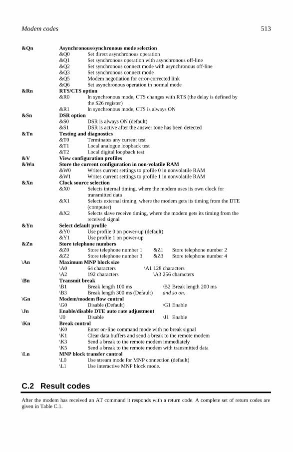
Modem codes 513
&Qn Asynchronous/synchronous mode selection &Q0 Set direct asynchronous operation &Q1 Set synchronous operation with asynchronous off-line &Q2 Set synchronous connect mode with asynchronous off-line &Q3 Set synchronous connect mode &Q5 Modem negotiation for error-corrected link &Q6 Set asynchronous operation in normal mode &Rn RTS/CTS option &R0 In synchronous mode, CTS changes with RTS (the delay is defined by the S26 register) &R1 In synchronous mode, CTS is always ON &Sn DSR option &S0 DSR is always ON (default) &S1 DSR is active after the answer tone has been detected &Tn Testing and diagnostics &T0 Terminates any current test &T1 Local analogue loopback test &T2 Local digital loopback test &V View configuration profiles &Wn Store the current configuration in non-volatile RAM &W0 Writes current settings to profile 0 in nonvolatile RAM &W1 Writes current settings to profile 1 in nonvolatile RAM &Xn Clock source selection &X0 Selects internal timing, where the modem uses its own clock for transmitted data &X1 Selects external timing, where the modem gets its timing from the DTE (computer) &X2 Selects slave receive timing, where the modem gets its timing from the received signal &Yn Select default profile &Y0 Use profile 0 on power-up (default) &Y1 Use profile 1 on power-up &Zn Store telephone numbers &Z0 Store telephone number 1 &Z1 Store telephone number 2 &Z2 Store telephone number 3 &Z3 Store telephone number 4 \An Maximum MNP block size \A0 64 characters \A1 128 characters \A2 192 characters \A3 256 characters \Bn Transmit break \B1 Break length 100 ms \B2 Break length 200 ms \B3 Break length 300 ms (Default) and so on. \Gn Modem/modem flow control \G0 Disable (Default) \G1 Enable \Jn Enable/disable DTE auto rate adjustment \J0 Disable \J1 Enable \Kn Break control \K0 Enter on-line command mode with no break signal \K1 Clear data buffers and send a break to the remote modem \K3 Send a break to the remote modem immediately \K5 Send a break to the remote modem with transmitted data \Ln MNP block transfer control \L0 Use stream mode for MNP connection (default) \L1 Use interactive MNP block mode.
C.2 Result codes After the modem has received an AT command it responds with a return code. A complete set of return codes are given in Table C.1.

514 Computer busses
Table C.1 Modem return codes
Message Digit Description OK 0 Command executed without errors CONNECT 1 A connection has been made RING 2 An incoming call has been detected NO CARRIER 3 No carrier detected ERROR 4 Invalid command CONNECT 1200 5 Connected to a 1200 bps modem NO DIAL-TONE 6 Dial-tone not detected BUSY 7 Remote line is busy NO ANSWER 8 No answer from remote line CONNECT 600 9 Connected to a 600 bps modem CONNECT 2400 10 Connected to a 2400 bps modem CONNECT 4800 11 Connected to a 4800 bps modem CONNECT 9600 13 Connected to a 9600 bps modem CONNECT 14400 15 Connected to a 14 400 bps modem CONNECT 19200 16 Connected to a 19200 bps modem CONNECT 28400 17 Connected to a 28400 bps modem CONNECT 38400 18 Connected to a 38400 bps modem CONNECT 115200 19 Connected to a 115200 bps modem FAX 33 Connected to a FAX modem in FAX mode DATA 35 Connected to a data modem in FAX mode CARRIER 300 40 Connected to V.21 or Bell 103 modem CARRIER 1200/75 44 Connected to V.23 backward channel carrier modem CARRIER 75/1200 45 Connected to V.23 forwards channel carrier modem CARRIER 1200 46 Connected to V.22 or Bell 212 modem CARRIER 2400 47 Connected to V.22 modem CARRIER 4800 48 Connected to V.32bis 4800 bps modem CONNECT 7200 49 Connected to V.32bis 7200 bps modem CONNECT 9600 50 Connected to V.32bis 9600 bps modem CONNECT 12000 51 Connected to V.32bis 12000 bps modem CONNECT 14400 52 Connected to V.32bis 14400 bps modem CONNECT 19200 61 Connected to a 19 200 bps modem CONNECT 28800 65 Connected to a 28 800 bps modem COMPRESSION: CLASS 5 66 Connected to modem with MNP Class 5 compression COMPRESSION: V.42bis 67 Connected to a V.42bis modem with compression COMPRESSION: NONE 69 Connection to a modem with no data compression PROTOCOL: NONE 70 PROTOCOL: LAPM 77 PROTOCOL: ALT 80
C.3 S-registers The modem contains various status registers called the S-registers which store modem settings. Table C.2 lists these registers. S14 Bitmapped options 0 1 Bit 1 E0 E1 Bit 2 Q0 Q1 Bit 3 V0 V1 Bit 4 Reserved Bit 5 T (tone dial) P (pulse dial) Bit 6 Reserved Bit 7 Answer mode Originate mode S16 Modem test mode register 0 1 Bit 0 Local analogue loopback Local analogue loopback

Modem codes 515
terminated test in progress Bit 2 Local digital loopback Local digital loopback terminated test in progress Bit 3 Remote modem analogue Remote modem analogue loopback test terminated loopback test in progress Bit 4 Remote modem digital Remote modem digital loopback test terminated loopback test in progress Bit 5 Remote modem digital Remote modem digital self-test terminated self-test in progress Bit 6 Remote modem analogue Remote modem analogue self-test terminated self-test in progress Bit 7 Unused S21 Bitmapped options 0 1 Bit 0 &J0 &J1 Bit 1 Bit 2 &R0 &R1 Bit 5 &C0 &C1 Bit 6 &S0 &S1 Bit 7 Y0 Y1 Bit 4, 3 = 00 &D0 Bit 4, 3 = 01 &D1 Bit 4, 3 = 10 &D2 Bit 4, 3 = 11 &D3 S22 Speaker/results bitmapped options Bit 1, 0 = 00 L0 Bit 1, 0 = 01 L1 Bit 1, 0 = 10 L2 Bit 1, 0 = 11 L3 Bit 3, 2 = 00 M0 Bit 3, 2 = 01 M1 Bit 3, 2 = 10 M2 Bit 3, 2 = 11 M3 Bit 6, 5, 4 = 000 X0 Bit 6, 5, 4 = 001 Reserved Bit 6, 5, 4 = 010 Reserved Bit 6, 5, 4 = 011 Reserved Bit 6, 5, 4 = 100 X1 Bit 6, 5, 4 = 101 X2 Bit 6, 5, 4 = 110 X3 Bit 6, 5, 4 = 111 X4 Bit 7 Reserved S23 Bitmapped options 0 1 Bit 0 &T5 &T4 Bit 3, 2, 1 = 000 300 bps communications rate Bit 3, 2, 1 = 001 600 bps communications rate Bit 3, 2, 1 = 010 1200 bps communications rate Bit 3, 2, 1 = 011 2400 bps communications rate Bit 3, 2, 1 = 100 4800 bps communications rate Bit 3, 2, 1 = 101 9600 bps communications rate Bit 3, 2, 1 = 110 19 200 bps communications rate Bit 3, 2, 1 = 111 Reserved Bit 5, 4 = 00 Even parity Bit 5, 4 = 01 Not used Bit 5, 4 = 10 Odd parity Bit 5, 4 = 11 No parity Bit 7, 6 = 00 G0 Bit 7, 6 = 01 G1 Bit 7, 6 = 10 G2 Bit 7, 6 = 11 G3

516 Computer busses
S23 Bitmapped options Bit 3, 1, 0 = 000 &M0 or &Q0 Bit 3, 1, 0 = 001 &M1 or &Q1 Bit 3, 1, 0 = 010 &M2 or &Q2 Bit 3, 1, 0 = 011 &M3 or &Q3 Bit 3, 1, 0 = 100 &Q3 Bit 3, 1, 0 = 101 &Q4 Bit 3, 1, 0 = 110 &Q5 Bit 3, 1, 0 = 111 &Q6 0 1 Bit 2 &L0 &L1 Bit 6 B0 B1 Bit 5, 4 = 00 X0 Bit 5, 4 = 01 X1 Bit 5, 4 = 10 X2 S28 Bitmapped options Bit 4, 3 = 00 &P0 Bit 4, 3 = 01 &P1 Bit 4, 3 = 10 &P2 Bit 4, 3 = 11 &P3 S31 Bitmapped options 0 1 Bit 1 N0 N1 Bit 3, 2 = 00 W0 Bit 3, 2 = 01 W1 Bit 3, 2 = 10 W2 S36 LAPM failure control Bit 2, 1, 0 = 000 Modem disconnect Bit 2, 1, 0 = 001 Modem stays on line and a direct mode connection Bit 2, 1, 0 = 010 Reserved Bit 2, 1, 0 = 011 Modem stays on line and normal mode connection is established Bit 2, 1, 0 = 100 An MNP connection is made, if it fails then the modem disconnects Bit 2, 1, 0 = 101 An MNP connection is made, if it fails then the modem makes a direct connection Bit 2, 1, 0 = 110 Reserved Bit 2, 1, 0 = 111 An MNP connection is made, if it fails then the modem makes a normal mode connection S37 Desired line connection speed Bit 3, 2, 1, 0 = 0000 Auto mode connection (F0) Bit 3, 2, 1, 0 = 0001 Modem connects at 300 bps (F1) Bit 3, 2, 1, 0 = 0010 Modem connects at 300 bps (F1) Bit 3, 2, 1, 0 = 0011 Modem connects at 300 bps (F1) Bit 3, 2, 1, 0 = 0100 Reserved Bit 3, 2, 1, 0 = 0101 Modem connects at 1200 bps (F4) Bit 3, 2, 1, 0 = 0110 Modem connects at 2400 bps (F5) Bit 3, 2, 1, 0 = 0111 Modem connects at V.23 (F3) Bit 3, 2, 1, 0 = 1000 Modem connects at 4800 bps (F6) Bit 3, 2, 1, 0 = 1001 Modem connects at 9600 bps (F8) Bit 3, 2, 1, 0 = 1010 Modem connects at 12 000 bps (F9) Bit 3, 2, 1, 0 = 1011 Modem connects at 144 000 bps (F10) Bit 3, 2, 1, 0 = 1100 Modem connects at 7200 bps (F7) S39 Flow control Bit 2, 1, 0 = 000 No flow control Bit 2, 1, 0 = 011 RTS/CTS (&K3) Bit 2, 1, 0 = 100 XON/XOFF (&K4) Bit 2, 1, 0 = 101 Transparent XON (&K5) Bit 2, 1, 0 = 110 RTS/CTS and XON/XOFF (&K6) S39 General bitmapped options Bit 5, 4, 3 = 000 \K0 Bit 5, 4, 3 = 001 \K1 Bit 5, 4, 3 = 010 \K2

Modem codes 517
Bit 5, 4, 3 = 011 \K3 Bit 5, 4, 3 = 100 \K4 Bit 5, 4, 3 = 101 \K5 Bit 7, 6 = 00 MNP 64 character block size (\A0) Bit 7, 6 = 01 MNP 128 character block size (\A1) Bit 7, 6 = 10 MNP 192 character block size (\A2) Bit 7, 6 = 11 MNP 256 character block size (\A3)
Table C.2 Modem registers
Register Function Range [typical default] S0 Rings to Auto-answer 0–255 rings [0 rings] S1 Ring counter 0–255 rings [0 rings] S2 Escape character [43] S3 Carriage return character [13] S6 Wait time for dial-tone 2–255 s [2 s] S7 Wait time for carrier 1–255 s [50 s] S8 Pause time for automatic dialing 0–255 s [2 s] S9 Carrier detect response time 1–255 in 0.1 s units [6] S10 Carrier loss disconnection time 1–255 in 0.1 s units [14] S11 DTMF tone duration 50–255 in 0.001 s units [95] S12 Escape code guard time 0–255 in 0.02 s units [50] S13 Reserved S14 General bitmapped options [8Ah (1000 1010b)] S15 Reserved S16 Test mode bitmapped options (&T) [0] S17 Reserved S18 Test timer 0–255 s [0] S19–S20 Reserved S21 V.24/General bitmapped options [04h (0000 0100b)] S22 Speak/results bitmapped options [75h (0111 0101b)] S23 General bitmapped options [37h (0011 0111b)] S24 Sleep activity timer 0–255 s [0] S25 Delay to DSR off 0–255 s [5] S26 RTS–CTS delay 0–255 in 0.01 s [1] S27 General bitmapped options [49h (0100 1001b)] S28 General bitmapped options [00h] S29 Flash dial modifier time 0–255 in 10 ms [0] S30 Disconnect inactivity timer 0–255 in 10 s [0] S31 General bitmapped options [02h (0000 0010b)] S32 XON character [Cntrl–Q, 11h (0001 0001b)] S33 XOFF character [Cntrl–S, 13h (0001 0011b)] S34–S35 Reserved S36 LAMP failure control [7] S37 Line connection speed [0] S38 Delay before forced hang-up 0–255 s [20] S39 Flow control [3] S40 General bitmapped options [69h (0110 1001b)] S41 General bitmapped options [3] S42–S45 Reserved S46 Data compression control [8Ah (1000 1010b)] S48 V.42 negotiation control [07h (0000 0111b)] S80 Soft-switch functions [0] S82 LAPM break control [40h (0100 0000b)] S86 Call failure reason code 0–255 S91 PSTN transmit attenuation level 0–15 dBm [10] S92 Fax transmit attenuation level 0–15 dBm [10] S95 Result code message control [0] S99 Leased line transmit level 0–15 dBm [10]

Redundancy checking
D.1 Cyclic redundancy check (CRC)
The CRC is one of the most reliable error detection schemes and can detect up to 95.5% of all errors. The most commonly used code is the CRC-16 standard code which is defined by the CCITT. The basic idea of a CRC can be illustrated using an example. Suppose the transmitter and receiver were both to agree that the numerical value sent by the transmitter would always be divisible by 9. Then should the receiver get a value which was not divisible by 9 then it would know that there was an error. For example, if a value of 32 were to be transmitted it could be changed to 320 so that the transmitter would be able to add to the least significant digit, making it divisible by 9. In this case the transmitter would add 4, making 324. If this transmitted value were to be corrupted in transmission then there would only be a 10% chance that an error would not be detected. In CRC-CCITT, the error correction code is 16 bits long and is the remainder of the data message polynomial G(x) divided by the generator polynomial P(x) (x16+x12+x5+1, i.e. 10001000000100001). The quotient is discarded and the remainder is truncated to 16 bits. This is then appended to the message as the coded word. The division does not use standard arithmetic division. Instead of the subtraction opera-tion an exclusive-OR operation is employed. This is a great advantage as the CRC only re-quires a shift register and a few XOR gates to perform the division. The receiver and the transmitter both use the same generating function P(x). If there are no transmission errors then the remainder will be zero. The method used is as follows: 1. Let P(x) be the generator polynomial and M(x) the message polynomial. 2. Let n be the number of bits in P(x). 3. Append n zero bits onto the right-hand side of the message so that it contains m+n bits. 4. Using modulo-2 division, divide the modified bit pattern by P(x). Modulo-2 arithmetic
involves exclusive-OR operations, i.e. 0-1=1, 1-1=0, 1-0=1 and 0-0=0. 5. The final remainder is added to the modified bit pattern. Example: For a 7-bit data code 1001100 determine the encoded bit pattern using a CRC generating polynomial of P(x) = x3 + x2 + x0. Show that the receiver will not detect an error if there are no bits in error. Answer P(x) = x3 + x2 + x0 (1101) G(x) = x6 + x3 + x2 (1001100) Multiply by the number of bits in the CRC polynomial:
D

520 Computer busses
x3(x6 + x3 + x2) x9 + x6 + x5 (1001100000) Figure D.1 shows the operations at the transmitter. The transmitted message is 1001100001 and Figure D.2 shows the operations at the receiver. It can be seen that the remainder is zero, so there have been no errors in the transmission. 1111101 1101 1001100000 1101 1001 1101 1000 1101 1010 1101 1110 1101 1100 1101 001
Figure D.1 CRC coding example
1111101 1101 1001100001 1101 1001 1101 1000 1101 1010 1101 1110 1101 1101 1101 000
Figure D.2 CRC decoding example
The CRC-CCITT is a standard polynomial for data communications systems and can detect: • All single and double bit errors. • All errors with an odd number of bit. • All burst errors of length 16 or less. • 99.997% of 17-bit error bursts. • 99.998% of 18-bit and longer bursts.

Redundancy checking 521
Table D.1 lists some typical CRC codes. CRC-32 is used in Ethernet, Token Ring and FDDI networks, whereas ATM uses CRC-8 and CRC-10.
Table D.1 Typical schemes
Type Polynomial Polynomial binary equivalent
CRC-8 x8+x2+x1+1 100000111 CRC-10 x10+x9+x5+ x4+x1 +1 11000110011 CRC-12 x12+x11+x3+ x2+1 1100000001101 CRC-16 x16+x15+x2+1 11000000000000101 CRC-CCITT x16+x12+x5+1 10001000000100001 CRC-32 x32+x26+x23+ x16+x12+x11
+x10+x8+x7+x5+x4+x2+x+1 100000100100000010001110110110111
D.1.1 Mathematical representation of the CRC
The main steps to CRC implementation are: 1. Prescale the input polynomial of )(' xM by the highest order of the generator polynomial
P(x). M x x M xn' ( ) ( )= 2. Next divide )(' xM by the generator polynomial to give:
)()(
)()(
)()()('
xGxRxQ
xGxMx
xGxM n
+==
which yields )()()()( xRxQxGxMx n += and rearranging gives )()()()( xQxGxRxMx n =+
This means that the transmitted message ( )()( xRxMx n + ) is now exactly divisible by G(x).
D.1.2 CRC example
Question A A CRC system uses a message of 1 + x2 + x4 + x5. Design a cyclic encoder circuit with genera-tor polynomial G(x) =1 + x2 + x3 and having appropriate gating circuitry to enable/disable the shift out of the CRC remainder. Answer A The generator polynomial is G(x) =1 + x2 + x3, the circuit is given in Figure D.3.

522 Computer busses
D1 D2 D3
M(x) Z
Figure D.3 CRC coder
Now to prove that this circuit does generate the polynomial. The output Z(x) will be
[ ]
( )Z x Z x x M x x Z x x x
Z x x x M x x
( ) ( ) ( ) ( )
( ) ( )
= + +
= + +
− − − −
− − −
1 2 2 1
3 1 3
Thus
( )
3
311)()(
−
−− ++=x
xxxZxM
giving
P x M xZ x
x x( ) ( )( )
= = + +3 2 1
Question B If the previous CRC system uses a message of 1 + x2 + x4 + x5 then determine the sequence of events that occur and hence determine the encoded message as a polynomial T(x). Synthesise the same code algebraically using modulo-2 division. Answer B First prescale the input polynomial of M(x) by x3, the highest power of G(x): M´(x)=x3M(x)= x3 + x5 + x7 + x8 The input is thus x3 + x5 + x7 + x8 (000101011), and the generated states are: Time M´(x) D1 D2 D3 D4 1 000101011 0 0 0 0 2 00010101 1 0 0 0 3 0001010 1 1 0 0 4 000101 0 1 1 1 5 00010 0 0 0 0 6 0001 0 0 0 0 7 000 1 0 0 0 8 00 0 1 0 0 9 0 0 0 1 1 10 1 0 1
LSD
MSD

Redundancy checking 523
The remainder is thus 101, so R(x) is x2 + 1. The transmitted polynomial will be T(x) = x3 M(x) + R(x) = x8 + x7 + x5 + x3 + x2 + 1 (110101101) To check this, use modulo-2 division to give
x3+x2+1 x8+x7+x5+x3
x8+x7+x5
x3
x3+x2+1
x2+1
x5 +1
Remainder This gives the same answer as the state table, i.e. x2+1. Prove that the transmitted message does not generate a remainder when divided by P(x). The transmitted polynomial, T(x), is x8 + x7 + x5 + x3 + x2 + 1 (110101101) and the generator polynomial, G(x), is 1+ x2+ x3. Thus
x3+ x2+ 1 x8+ x7+ x5+ x3+ x2+ 1x8+ x7+ x5
x3+ x2+ 1x3+ x2+ 1
0
x5 +1
Remainder As there is a zero remainder, there is no error.
D.2 Longitudinal/vertical redundancy checks (LRC/VRC)
RS-232 uses vertical redundancy checks (VRC) when it adds a parity bit to the transmitted character. Longitudinal (or horizontal) redundancy checks (LRC) adds a parity bit for all bits in the message at the same bit position. Vertical coding operates on a single character and is known as character error coding. Horizontal checks operate on groups of characters and de-scribed as message coding. LRC always uses even parity and the parity bit for the LRC char-acter has the parity of the VRC code. In the example given next, the character sent for LRC is thus 10101000 (28h) or a ‘(’. The message sent is ‘F’, ‘r’, ‘e’, ‘d’, ‘d’, ‘y’ and ‘(’. Without VR checking, LR checking detects most errors but does not detect errors where an even number of characters have an error in the same bit position. In the previous example if bit 2 of the ‘F’ and ‘r’ were in error then LRC would be valid.

524 Computer busses
This problem is overcome if LRC and VRC are used together. With VRC/LRC the only time an error goes undetected is when an even number of bits, in an even number of charac-ters, in the same bit positions of each character are in error. This is of course very unlikely. On systems where only single-bit errors occur, the LRC/VRC method can be used to de-tect and correct the single-bit error. For systems where more than one error can occur it is not possible to locate the bits in error, so the receiver prompts the transmitter to retransmit the message. Example A communications channel uses ASCII character coding and LRC/VRC bits are added to each word sent. Encode the word ‘Freddy’ and, using odd parity for the VRC and even parity for the LRC; determine the LRC character. Answer
F r e d d y LRC
b0 0 0 1 0 0 1 0 b1 1 1 0 0 0 0 0 b2 1 0 1 1 1 0 0 b3 0 0 0 0 0 1 1 b4 0 1 0 0 0 1 0 b5 0 1 1 1 1 1 1 b6 1 1 1 1 1 1 0
VRC 0 1 1 0 0 0 1

ASCII Character Code
E.1 Standard ASCII
ANSI defined a standard alphabet known as ASCII. This has since been adopted by the CCITT as a standard, known as IA5 (International Alphabet No. 5). The following tables de-fine this alphabet in binary, as a decimal value, as a hexadecimal value and as a character. Binary Decimal Hex Character Binary Decimal Hex Character 00000000 0 00 NUL 00010000 16 10 DLE 00000001 1 01 SOH 00010001 17 11 DC1 00000010 2 02 STX 00010010 18 12 DC2 00000011 3 03 ETX 00010011 19 13 DC3 00000100 4 04 EOT 00010100 20 14 DC4 00000101 5 05 ENQ 00010101 21 15 NAK 00000110 6 06 ACK 00010110 22 16 SYN 00000111 7 07 BEL 00010111 23 17 ETB 00001000 8 08 BS 00011000 24 18 CAN 00001001 9 09 HT 00011001 25 19 EM 00001010 10 0A LF 00011010 26 1A SUB 00001011 11 0B VT 00011011 27 1B ESC 00001100 12 0C FF 00011100 28 1C FS 00001101 13 0D CR 00011101 29 1D GS 00001110 14 0E SO 00011110 30 1E RS 00001111 15 0F SI 00011111 31 1F US
Binary Decimal Hex Character Binary Decimal Hex Character 00100000 32 20 SPACE 00110000 48 30 0 00100001 33 21 ! 00110001 49 31 1 00100010 34 22 “ 00110010 50 32 2 00100011 35 23 # 00110011 51 33 3 00100100 36 24 $ 00110100 52 34 4 00100101 37 25 % 00110101 53 35 5 00100110 38 26 & 00110110 54 36 6 00100111 39 27 / 00110111 55 37 7 00101000 40 28 ( 00111000 56 38 8 00101001 41 29 ) 00111001 57 39 9 00101010 42 2A * 00111010 58 3A : 00101011 43 2B + 00111011 59 3B ; 00101100 44 2C , 00111100 60 3C < 00101101 45 2D - 00111101 61 3D = 00101110 46 2E . 00111110 62 3E > 00101111 47 2F / 00111111 63 3F ?
E

526 Computer busses
Binary Decimal Hex Character Binary Decimal Hex Character 01000000 64 40 @ 01010000 80 50 P
01000001 65 41 A 01010001 81 51 Q
01000010 66 42 B 01010010 82 52 R
01000011 67 43 C 01010011 83 53 S
01000100 68 44 D 01010100 84 54 T
01000101 69 45 E 01010101 85 55 U
01000110 70 46 F 01010110 86 56 V
01000111 71 47 G 01010111 87 57 W
01001000 72 48 H 01011000 88 58 X
01001001 73 49 I 01011001 89 59 Y
01001010 74 4A J 01011010 90 5A Z
01001011 75 4B K 01011011 91 5B [
01001100 76 4C L 01011100 92 5C \
01001101 77 4D M 01011101 93 5D ]
01001110 78 4E N 01011110 94 5E ‘
01001111 79 4F O 01011111 95 5F _
Binary Decimal Hex Character Binary Decimal Hex Character 01100000 96 60 01110000 112 70 p
01100001 97 61 a 01110001 113 71 q
01100010 98 62 b 01110010 114 72 r
01100011 99 63 c 01110011 115 73 s
01100100 100 64 d 01110100 116 74 t
01100101 101 65 e 01110101 117 75 u
01100110 102 66 f 01110110 118 76 v
01100111 103 67 g 01110111 119 77 w
01101000 104 68 h 01111000 120 78 x
01101001 105 69 i 01111001 121 79 y
01101010 106 6A j 01111010 122 7A z
01101011 107 6B k 01111011 123 7B
01101100 108 6C l 01111100 124 7C :
01101101 109 6D m 01111101 125 7D
01101110 110 6E n 01111110 126 7E ~
01101111 111 6F o 01111111 127 7F DEL

ASCII 527
E.2 Extended ASCII code
The standard ASCII character has 7 bits and the basic set ranges from 0 to 127. This code is rather limited as it does not contains symbols such as Greek letters, lines, and so on. For this purpose the extended ASCII code has been defined. This fits into character numbers 128 to 255. The following four tables define a typical extended ASCII character set. Binary Decimal Hex Character Binary Decimal Hex Character 10000000 128 80 Ç 10010000 144 90 É
10000001 129 81 ü 10010001 145 91 æ
10000010 130 82 é 10010010 146 92 Æ
10000011 131 83 â 10010011 147 93 ô
10000100 132 84 ä 10010100 148 94 ö
10000101 133 85 à 10010101 149 95 ò
10000110 134 86 å 10010110 150 96 û
10000111 135 87 ç 10010111 151 97 ù
10001000 136 88 ê 10011000 152 98 ÿ
10001001 137 89 ë 10011001 153 99 Ö
10001010 138 8A è 10011010 154 9A Ü
10001011 139 8B ï 10011011 155 9B ¢
10001100 140 8C î 10011100 156 9C £
10001101 141 8D ì 10011101 157 9D ¥
10001110 142 8E Ä 10011110 158 9E ₧ 10001111 143 8F Å 10011111 159 9F ƒ Binary Decimal Hex Character Binary Decimal Hex Character 10100000 160 A0 á 10110000 176 B0 10100001 161 A1 í 10110001 177 B1 10100010 162 A2 ó 10110010 178 B2 10100011 163 A3 ú 10110011 179 B3 10100100 164 A4 ñ 10110100 180 B4 10100101 165 A5 Ñ 10110101 181 B5 10100110 166 A6 ª 10110110 182 B6 10100111 167 A7 º 10110111 183 B7 10101000 168 A8 ¿ 10111000 184 B8 10101001 169 A9 10111001 185 B9 10101010 170 AA ¬ 10111010 186 BA 10101011 171 AB ½ 10111011 187 BB 10101100 172 AC ¼ 10111100 188 BC 10101101 173 AD ¡ 10111101 189 BD 10101110 174 AE « 10111110 190 BE 10101111 175 AF » 10111111 191 BF

528 Computer busses
Binary Decimal Hex Character Binary Decimal Hex Character 11000000 192 C0 11010000 208 D0 11000001 193 C1 11010001 209 D1 11000010 194 C2 11010010 210 D2 11000011 195 C3 11010011 211 D3 11000100 196 C4 11010100 212 D4 11000101 197 C5 11010101 213 D5 11000110 198 C6 11010110 214 D6 11000111 199 C7 11010111 215 D7 11001000 200 C8 11011000 216 D8 11001001 201 C9 11011001 217 D9 11001010 202 CA 11011010 218 DA 11001011 203 CB 11011011 219 DB 11001100 204 CC 11011100 220 DC 11001101 205 CD 11011101 221 DD 11001110 206 CE 11011110 222 DE 11001111 207 CF 11011111 223 DF Binary Decimal Hex Character Binary Decimal Hex Character 11100000 224 E0 α 11110000 240 F0 Ξ 11100001 225 E1 ß 11110001 241 F1 ± 11100010 226 E2 Γ 11110010 242 F2 ≥ 11100011 227 E3 π 11110011 243 F3 ≤ 11100100 228 E4 Σ 11110100 244 F4 ⌠ 11100101 229 E5 σ 11110101 245 F5 ⌡ 11100110 230 E6 µ 11110110 246 F6 ÷ 11100111 231 E7 τ 11110111 247 F7 ≈ 11101000 232 E8 Φ 11111000 248 F8 ° 11101001 233 E9 Θ 11111001 249 F9 · 11101010 234 EA Ω 11111010 250 FA ·
11101011 235 EB δ 11111011 251 FB √ 11101100 236 EC ϕ 11111100 252 FC ⁿ 11101101 237 ED φ 11111101 253 FD ²
11101110 238 EE Ε 11111110 254 FE 11101111 239 EF Λ 11111111 255 FF

Quick Reference
Parallel port Serial port Pin Name Pin Name Pin Name Pin Name 1 Strobe 14 GND 1 DCD 6 CTS 2 Auto Feed 15 D6 2 DSR 7 DTR 3 D0 16 GND 3 RX 8 RI 4 Error 17 D7 4 RTS 9 GND 5 D1 18 GND 5 TX 6 INIT 19 ACK 7 D2 20 GND 8 SLCT IN 21 BUSY 9 D3 22 GND 10 GND 23 PE 11 D4 24 GND 12 GND 25 SLCT 13 D5 IDE Floppy disk Pin Name Pin Name Pin Name Pin Name 1 Reset 2 GND 1 GND 2 FDHDIN 3 D7 4 D8 3 GND 4 Reserved 5 D6 6 D9 5 Key 6 FDEDIN 7 D5 8 D10 7 RTS 8 -Index 9 D4 10 D11 9 GND 10 Motor En A 11 D3 12 D12 11 GND 12 Drive Sel B 13 D2 14 D13 13 GND 14 Drive Sel A 15 D1 16 D14 15 GND 16 Motor En B 17 D0 18 D15 17 GND 18 DIR 19 GND 20 Key 19 GND 20 STEP 21 DRQ3 22 GND 21 GND 22 Write Data 23 -I/O W 24 GND 23 GND 24 Write Gate 25 -I/O R 26 GND 25 GND 26 Track 00 27 IOCHRDY 28 BALE 27 GND 28 Write Protect 29 -DACK3 30 GND 29 GND 30 Read Data 31 IRQ14 32 IOCS16 31 GND 32 Side 1 Sel 33 ADD 1 34 GND 33 GND 34 Diskette 35 ADD 0 36 ADD 2 37 -CS 0 38 CS 1 39 ACTIVITY 40 GND Bus connections Page Bus connections Page AGP 205 Cache 126 CAN bus 336 Games port 192 IDE/ISA 144 IEEE-1394 347 IEEE-488 bus 190 ISA bus 88
F

530 Computer busses
Keyboard 196 Parallel Port 272 PCI bus 105 PCMCIA 174 PIIX3 123 RS-232 (modem) 232 RS-232 (null modem) 230 RS-232 232 SCSI 159 SCSI-II 160 TXC 125 USB 182 VESA VL-Local Bus 509 Typical IRQs Typical DMA channels 0 Internal timer 1 Keyboard 0 Any 2 Cascaded interrupt 3 COM2 1 Any 4 COM1 5 (Soundcard) 2 Floppy disk 6 Floppy disk 7 LPT1 3 Parallel port 8 Real-time clock 9 User available 4 Cascaded DMA 10 User available 11 (PCI steering) 5 Any 12 Serial bus mouse (if any) 13 Math coprocessor 6 Any 14 Primary IDE 15 Secondary IDE 7 Any Example I/O map 0000–000F Slave DMA controller 0020–0021 Master PIC 0040–0043 System timer 0060 Keyboard 0061 Speaker 0064 Keyboard 0070–0071 Real-time clock 0080–008F DMA 00A0–00A1 Slave PIC 00F0–00FF Numeric processor 0170–0177 Secondary H/D 0200–020F Game port 0220–022F Soundcard 0294–0297 PCI bus 02F8–02FF COM2 0330–0331 Soundcard 0370–0371 Soundcard 0376 Secondary IDE 0378–037A LPT1 0388–03B8 Soundcard 03B0–03BB VGA 03C0–03DF VGA 03F6 Primary IDE 03F8–03FF COM1 0480–048F PCI bus 04D0–04D1 PCI bus 0530–0537 Soundcard 0778–077A ECP Port (LPT1) 0CF8–0CFF PCI bus 4000–403F PCI bus 5000–5018 PCI bus D000–DFFF AGP controller E000–E01F USB controller E400–E4FF VGA

ASCII 531
Bus specification Bus Max.
throughput Data bus (bits)
Address bus (bits)
Notes
AGP 500 MB/s 64 32 EISA 32 MB/s 32 32 4 GB max address,
8 MHz clock Ethernet 1.25 MB/s 1 N/A 10 Mbps (10BASE) Fibre Channel
132.5 MB/s 1 N/A 1.06 Gbps
Firewire 50 MB/s 1 N/A 400 Mbps (S400) IDE 16.6 MB/s 16 N/A Mode 4, EIDE, Maximum 4 devices IEEE-488 1 MB/s 8 N/A ISA 16 MB/s 16 24 16 MB max address, 8 MHz clock ISDN 16 kB/s 1 N/A 2×64 kbps MCA 100 MB/s 32 32 Modem 7 kB/s 1 N/A 56 kbps Parallel port 150 kB/s 8 N/A 150 kB/s is equivalent to 1.2 Mbps
which is the required transfer rate for stereo, 44.1kHz, 16-bit sampled audio
Parallel port (ECP/EPP)
1.2 MB/s 8 N/A ×8
PC 8 MB/s 8 20 1 MB max address, 8 MHz clock PCI 132 MB/s 32 32 33 MHz clock PCI (32-bit) 132 MB/s 32 32 33 MHz clock PCI (64-bit) 264 MB/s 64 32 33 MHz clock PCMCIA 16 MB/s 16 26 64 MB max address RS-232 14.4 kB/s 1 N/A 115.2 kbps RS-485 1.25 MB/s 1 N/A 10 Mbps SCSI (Fast/wide)
40 MB/s 16 N/A 20 MHz clock
SCSI-I 5 MB/s 8 N/A SCSI-II (Wide)
20 MB/s 16 N/A 10 MHz clock
SCSI-II (Fast) 10 MB/s 8 N/A 10 MHz clock USB 1.5 MB/s 1 N/A 12 Mbps VL 132 MB/s 32 32 33 MHz clock
F.1 Notes from the author
Well, the book in nearly finished, so as a last little bit of fun here is a final league table for the busses. They are graded on usefulness (how useful it is in its application, and how well it can be used on other systems), availability (the ease that it can be purchased, and the num-ber of applications that it has), data throughput (the speed of data throughput), cost (how expensive it is to purchase applications which use the bus) and configuration (how well and how easy it is to configure the bus). From the table it can be seen that the winners are the PCI bus and Ethernet (100BASE).
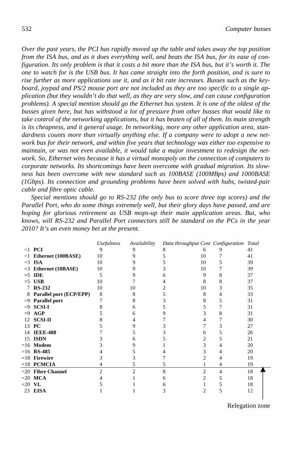
532 Computer busses
Over the past years, the PCI has rapidly moved up the table and takes away the top position from the ISA bus, and as it does everything well, and beats the ISA bus, for its ease of con-figuration. Its only problem is that it costs a bit more than the ISA bus, but it’s worth it. The one to watch for is the USB bus. It has came straight into the forth position, and is sure to rise further as more applications use it, and as it bit rate increases. Busses such as the key-board, joypad and PS/2 mouse port are not included as they are too specific to a single ap-plication (but they wouldn’t do that well, as they are very slow, and can cause configuration problems). A special mention should go the Ethernet bus system. It is one of the oldest of the busses given here, but has withstood a lot of pressure from other busses that would like to take control of the networking applications, but it has beaten of all of them. Its main strength is its cheapness, and it general usage. In networking, more any other application area, stan-dardness counts more than virtually anything else. If a company were to adopt a new net-work bus for their network, and within five years that technology was either too expensive to maintain, or was not even available, it would take a major investment to redesign the net-work. So, Ethernet wins because it has a virtual monopoly on the connection of computers to corporate networks. Its shortcomings have been overcome with gradual migration. Its slow-ness has been overcome with new standard such as 100BASE (100MBps) and 1000BASE (1Gbps). Its connection and grounding problems have been solved with hubs, twisted-pair cable and fibre optic cable. Special mentions should go to RS-232 (the only bus to score three top scores) and the Parallel Port, who do some things extremely well, but their glory days have passed, and are hoping for glorious retirement as USB mops-up their main application areas. But, who knows, will RS-232 and Parallel Port connectors still be standard on the PCs in the year 2010? It’s an even money bet at the present. Usefulness Availability Data throughput Cost Configuration Total =1 PCI 9 9 8 6 9 41 =1 Ethernet (100BASE) 10 9 5 10 7 41 =3 ISA 10 9 5 10 5 39 =3 Ethernet (10BASE) 10 9 3 10 7 39 =5 IDE 5 9 6 9 8 37 =5 USB 10 7 4 8 8 37 7 RS-232 10 10 2 10 3 35 8 Parallel port (ECP/EPP) 8 8 5 8 4 33 =9 Parallel port 7 8 3 8 5 31 =9 SCSI-I 8 6 5 5 7 31 =9 AGP 5 6 9 3 8 31 12 SCSI-II 8 4 7 4 7 30 13 PC 5 9 3 7 3 27 14 IEEE-488 7 5 3 6 5 26 15 ISDN 3 6 5 2 5 21 =16 Modem 3 9 1 3 4 20 =16 RS-485 4 5 4 3 4 20 =18 Firewire 3 3 7 2 4 19 =18 PCMCIA 4 5 5 1 4 19 =20 Fibre Channel 2 2 8 2 4 18 =20 MCA 4 1 6 2 5 18 =20 VL 5 1 6 1 5 18 23 EISA 1 1 3 2 5 12
Relegation zone
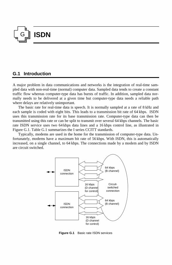
ISDN
G.1 Introduction
A major problem in data communications and networks is the integration of real-time sam-pled data with non-real-time (normal) computer data. Sampled data tends to create a constant traffic flow whereas computer-type data has bursts of traffic. In addition, sampled data nor-mally needs to be delivered at a given time but computer-type data needs a reliable path where delays are relatively unimportant. The basic rate for real-time data is speech. It is normally sampled at a rate of 8 kHz and each sample is coded with eight bits. This leads to a transmission bit rate of 64 kbps. ISDN uses this transmission rate for its base transmission rate. Computer-type data can then be transmitted using this rate or can be split to transmit over several 64 kbps channels. The basic rate ISDN service uses two 64 kbps data lines and a 16 kbps control line, as illustrated in Figure G.1. Table G.1 summarizes the I series CCITT standards. Typically, modems are used in the home for the transmission of computer-type data. Un-fortunately, modems have a maximum bit rate of 56 kbps. With ISDN, this is automatically increased, on a single channel, to 64 kbps. The connections made by a modem and by ISDN are circuit switched.
Circuit-switched
connection
ISDNconnection
64 kbps (B channel)
ISDNconnection
64 kbps (B channel)
16 kbps (D channelfor control)
16 kbps (D channelfor control)
Figure G.1 Basic rate ISDN services
G

534 Computer busses
Table G.1 CCITT standards on ISDN
CCITT standard number Description I.1XX ISDN terms and technology I.2XX ISDN services I.3XX ISDN addressing I.430 and I.431 ISDN physical layer interface I.440 and I.441 ISDN data layer interface I.450 and I.451 ISDN network layer interface I.5XX ISDN internetworking I.6XX ISDN maintenance
The great advantage of an ISDN connection is that the type of data transmitted is irrele-vant to the transmission and switching circuitry. Thus, it can carry other types of digital data, such as facsimile, teletex, videotex and computer data. This reduces the need for modems, which convert digital data into an analogue form, only for the public telephone network to convert the analogue signal back into a digital form for transmission over a digital link. It is also possible to multiplex the basic rate of 64 kbps to give even higher data rates. This multi-plexing is known as N × 64 kbps or broadband ISDN (B-ISDN). Another advantage of ISDN is that it is a circuit-switched connection where a permanent connection is established between two nodes. This connection is guaranteed for the length of the connection. It also has a dependable delay time and is thus suited to real-time data.
G.2 ISDN channels
ISDN uses channels to identify the data rate, each based on the 64 kbps provision. Typical channels are B, D, H0, H11 and H12. The B-channel has a data rate of 64 kbps and provides a circuit-switched connection between endpoints. A D-channel operates at 16 kbps and it controls the data transfers over the B channels. The other channels provide B-ISDN for much higher data rates. Table G.2 outlines the basic data rates for these channels. The two main types of interface are the basic rate access and the primary rate access. Both are based around groupings of B- and D-channels. The basic rate access allows two B-channels and one 16 kbps D-channel. Primary rate provides B-ISDN, such as H12 which gives 30 B-channels and a 64 kbps D-channel. For basic and primary rates, all channels multiplex onto a single line by combining channels into frames and adding extra synchronisation bits. Figure G.2 gives examples of the basic rate and primary rate.
Table G.2 ISDN channels
Channel Description B 64 kbps D 16 kbps signaling for channel B (ISDN)
64 kbps signaling for channel B (B-ISDN) H0 384 kbps (6 × 64 kbps) for B-ISDN H11 1.536 Mbps (24 × 64 kbps) for B-ISDN H12 1.920 Mbps (30 × 64 kbps) for B-ISDN

ISDN 535
Channel 1 (64 kbps)Channel 2 (64 kbps)
Signalling information (16 kbps)
192 kbps(Channel 1,Channel 2,Signalling info.and extra framing bits)
Channel 1 (64 kbps)Channel 2 (64 kbps)
Signalling information (64 kbps)
1.544 Mbps(Channel 1..24,Signalling info.and extra framing bits) Channel 24 (64 kbps)
Channel 1 (64 kbps)
Channel 2 (64 kbps)
Signalling information (64 kbps)
2.048 Mbps(Channel 1..30,Signalling info.and extra framing bits) Channel 30 (64 kbps)
Basic rate ISDNData rate:128 kbps
Primary rateISDN (H11)Data rate:
1.536 Mbps
Primary rateISDN (H12)Data rate:
1.920 Mbps
Figure G.2 Basic rate, H11 and H12 ISDN services
The basic rate ISDN gives two B-channels at 64 kbps and a signalling channel at 16 kbps. These multiplex into a frame and, after adding extra framing bits, the total output data rate is 192 kbps. The total data rate for the basic rate service is thus 128 kbps. One or many devices may multiplex their data, such as two devices transmitting at 64 kbps, a single device multi-plexing its 128 kbps data over two channels (giving 128 kbps), or by several devices trans-mitting a sub-64 kbps data rate over the two channels. For example, four 32 kbps devices could simultaneously transmit their data, eight 16 kbps devices, and so on. For H12, 30 × 64 kbps channels multiplex with a 64 kbps-signalling channel, and with ex-tra framing bits, the resulting data rate is 2.048 Mbps (compatible with European PCM-TDM systems). This means the actual data rate is 1.920 Mbps. As with the basic service this could contain a number of devices with a data rate of less than or greater than a multiple of 64 kbps. For H11, 24 × 64 kbps channels multiplex with a 64 kbps-signalling channel, and with ex-tra framing bits, it produces a data rate of 1.544 Mbps (compatible with USA PCM-TDM systems). The actual data rate is 1.536 Mbps.
G.3 ISDN physical layer interfacing
The physical layer corresponds to layer 1 of the OSI seven-layer model and is defined in CCITT specifications I.430 and I.431. Pulses on the line are not coded as pure binary, they use a technique called alternate mark inversion (AMI).

536 Computer busses
G.3.1 Alternative mark inversion (AMI) line code
AMI line codes use three voltage levels. In pure AMI, 0 V represents a ‘0’, and the voltage amplitude for each ‘1’ is the inverse of the previous ‘1’ bit. ISDN uses the inverse of this, i.e. 0 V for a ‘1’ and an inverse in voltage for a ‘0’, as shown in Figure G.3. Normally the pulse amplitude is 0.75 V. Inversion of the AMI signal (i.e. inverting a ‘0’ rather than a ‘1’) allows for timing in-formation to be recovered when there are long runs of zeros, which is typical in the idle state. AMI line code also automatically balances the signal voltage, and the average voltage will be approximately zero even when there are long runs of zeros (this is a requirement as the con-nection to the network is transformer coupled).
1 0 0 1 1 0 1 1 0 0 0 0
0V
+V
-V
Figure G.3 AMI used in ISDN
G.3.2 System connections
In basic rate connections, up to eight devices, or items of termination equipment (TE), can connect to the network termination (NT). They connect over a common four-wire bus using two sets of twisted-pair cables. The transmit output (TX) on each TE connects to the transmit output on the other TEs, and the receive input (RX) on each TE connects to all other TEs. On the NT the receive input connects to the transmit of the TEs, and the transmit output of the NT connects to the receive input of the TEs. A contention protocol allows only one TE to communicate at a time. An 8-pin ISO 8877 connector connects a TE to the NT; this is similar to the RJ-45 con-nector. Figure G.4 shows the pin connections. Pins 3 and 6 carry the TX signal from the TE, pins 4 and 5 provide the RX to the TEs. Pins 7 and 8 are the secondary power supply from the NT and pins 1 and 2 the power supply from the TE (if used). The TX/RX lines connect via transformers, thus only the AC part of the bitstream transfers into the PCM circuitry of the TE and the NT. This produces a need for a balanced DC line code such as AMI, as the DC component in the bitstream will not pass through the transformers.
G.3.3 Frame format
Figures G.5 and G.6 show the ISDN frame formats. Each frame is 250 µs long and contains 48 bits; this give a total bit rate of 192 kbps (48/250 × 10-6) made up of two 64 kbps B chan-nels, one 16 kbps D-channel and extra framing, DC balancing and synchronisation bits. The F/L pair of bits identify the start of each transmitted frame. When transmitting from a TE to an NT there is a 10-bit offset in the return of the frame back to the TE. The E bits echo the D-channel bits back to the TE.

ISDN 537
Powersource1
Powersink1
NT
TX
RX
RX
TX
Powersource2
Powersink2
Termination equipment
2
6
5
47
8
Powersource3
1
3
2
3
4
57
8
6
1
Networktermination
+
-
Figure G.4 Power supplies between NT and TE
B1 channel
EDAFAN
B2 channel
EDS
B1 channel
EDS
B2 channel
LEDFL010
48 bits in 250 µs
Figure G.5 ISDN frame format for NT to TE
B1 channel
L D L FAL
B2 channel
L D L
B1 channel
L D L
B2 channel
LL DF L
010
48 bits in 250 µ s
Figure G.6 ISDN frame format for TE to NT
where F – framing bit N – set to a 1 L – DC balancing bit D – D-channel bit E – D-echo channel bit FA – auxiliary framing bit (= 0) S – reserved for future use A – activation bit M – multiframing bit B1 – bits for channel 1 B2 – bits for channel 2 When transmitting from the NT to the TE, the bits after the F/L bits, in the B-channel, have a volition in the first 0. If any of these bits is a 0 then a volition will occur, but if they are 1s then no volition can occur. To overcome this the FA bit forces a volition. As it is followed by

538 Computer busses
0 (the N bit) it will not be confused with the F/L pair. The start of the frame can thus be traced backwards to find the F/L pair. There are 16 bits for each B-channel, giving a basic data rate of 64 kbps (16/250 × 10-6) and there are 4 bits in the frame for the D-channel, giving a bit rate of 16 kbps (4/250 × 10-6). The L bit balances the DC level on the line. If the number of zeros following the last bal-ancing bit is odd then the balancing bit is a 0, else it is a 1. When synchronised the NT in-forms the TEs by setting the A bit.
G.4 ISDN data link layer
The data link layer uses a protocol known as the link access procedure for the D-channel (LAPD). Figure G.7 shows the frame format. The unique bit sequence 01111110 identifies the start and end of the frame. This bit pattern cannot occur in the rest of the frame due to zero bit-stuffing. The address field contains information on the type of data contained in the frame (the service access point identifier) and the physical address of the ISDN device (the terminal endpoint identifier). The control field contains a supervisory, an unnumbered or an informa-tion frame. The frame check sequence provides error detection information.
Networkdata
Frame checksequence
Controlfield
Addressfield01111110 01111110
Startdelimiter
Enddelimiter
Service accesspoint identifer (SAPI) C/R EA0 Terminal endpoint
identifier (TEI) EA1
Figure G.7 D-channel frame structure
G.4.1 Address field
The data link address only contains addressing information to connect the TE to the NT and does not have network addresses. Figure G.7 shows the address field format. The SAPI iden-tifies the type of ISDN service. For example, a frame from a telephone would be identified as such, and only telephones would read the frame. All TEs connect to a single multiplexed bus, thus each has a unique data link address, known as a terminal endpoint identifier (TEI). The user or the network sets this; the ranges of available addresses are:
0–63 non-automatic assignment TEIs 64–126 automatic assignment TEIs 127 global TEI

ISDN 539
The non-automatic assignment involves the user setting the address of each of the devices connected to the network. When a device transmits data it inserts its own TEI address and only receives data which has its TEI address. In most cases devices should not have the same TEI address, as this would cause all devices with the same TEI address, and the SAPI, to re-ceive the same data (although, in some cases, this may be a requirement). The network allocates addresses to devices requiring automatic assignment before they can communicate with any other devices. The global TEI address is used to broadcast mes-sages to all connected devices. A typical example is when a telephone call is incoming to a group on a shared line where all the telephones would ring until one was answered. The C/R bit is the command/response bit and EA0/EA1 are extended address field bits.
G.4.2 Bit stuffing
With zero bit stuffing the transmitter inserts a zero into the bitstream when transmitting five consecutive 1s. When the receiver receives five consecutive 1s it deletes the next bit if it is a zero. This stops the unique 01111110 sequence occurring within the frame. For example if the bits to be transmitted are
101000101011111100001010001010000111110101010 then with the start and end delimiter this would be
0111111010100010101111110000101000101000011111010101001111110 It can be seen from this bitstream that the stream to be transmitted contains the delimiter within the frame. This zero bit insertion is applied to give
011111101010001010111110100001010001010000111110010101001111110 Notice that the transmitter has inserted a zero when five consecutive 1s occur. Thus the bit pattern 01111110 cannot occur anywhere in the bitstream. When the receiver receives five consecutive 1s it deletes the next bit if it is a zero. If it is a 1 then it is a valid delimiter. In the example the received stream will be
0111111010100010101111110000101000101000011111010101001111110
G.4.3 Control field
ISDN uses a 16-bit control field for information and supervisory frames and an 8-bit field for unnumbered frames, as illustrated in Figure G.8. Information frames contain sequenced data. The format is 0SSSSSSSXRRRRRRR, where SSSSSSS is the send sequence number and RRRRRRR is the frame sequence number that the sender expects to receive next (X is the poll/final bit). As the extended mode uses a 7-bit sequence field then information frames are numbered from 0 to 127. Supervisory frames contain flow control data. Table G.3 lists the supervisory frame types and the control field bit settings. The RRRRRRR value represent the 7-bit receive sequence number.

540 Computer busses
Information frame
Supervisory frame
Unnumbered frame
Address Control Info FCS01111110 01111110
8/16 bits
P/F N(R)0 N(S)
1
1
0 S 0 0 0 0 P/F N(R)
1 M P/F M
M – modifier function bitsS – supervisory function bits
Figure G.8 ISDN control field
Table G.3 Supervisory frame types and control field settings
Type Control field setting Receiver ready (RR) 10000000PRRRRRRR Receiver not ready (RNR) 10100000PRRRRRRR Reject (REJ) 10010000PRRRRRRR
Unnumbered frames set up and clear connections between a node and the network. Table G.4 lists the unnumbered frame commands and Table G.5 lists the unnumbered frame responses.
Table G.4 Unnumbered frame commands and control field settings
Type Control field setting Set asynchronous balance mode extended (SABME) 1111P110 Unnumbered information (UI) 1100F000 Disconnect mode (DISC) 1100P010
Table G.5 Unnumbered frame responses and control field settings
Type Control field setting Disconnect mode (DM) 1111P110 Unnumbered acknowledgment (UA) 1100F000 Frame reject (FRMR) 1110P001
In ISDN all connected nodes and the network connection can send commands and re-ceive responses. Figure G.9 shows a sample connection of an incoming call to an ISDN node (address TEI_1). The SABME mode is set up initially using the SABME command (U[SABME,TEI_1,P=1]), followed by an acknowledgement from the ISDN node (U[UA,TEI_1,F=1]). At any time, either the network or the node can disconnect the con-nection. In this case the ISDN node disconnects the connection with the command U[DISC,TEI_1,P=1]. The network connection acknowledges this with an unnumbered ac-knowledgement (U[UA,TEI_1,F=1]).

ISDN 541
U[SABME,TEI_1,P=1]
U[UA,TEI_1,F=1
]
U[DISC,TEI_1,P
=1]
U[UA,TEI_1,F=1]
Network connection ISDN node
Data flow
TEI_1
Incomingcall
Figure G.9 Example connection between a primary/secondary
G.4.4 D-channel contention
The D-channel contention protocol ensures that only one terminal can transmit its data at a time. This happens because the start and the end of the D-channel bits have the bitstream 01111110, as shown below:
1111101111110XXXXXXXXX...XXXXXXXX011111101111 When idle, each TE floats to a high-impedance state, which is taken as a binary 1. To trans-mit, a TE counts the number of 1s in the D-channel. A 0 resets this count. After a predeter-mined number, greater than a predetermined number of consecutive 1s, the TE transmits its data and monitors the return from the NT. If it does not receive the correct D-channel bit-stream returned through the E bits then a collision has occurred. When a TE detects a colli-sion it immediately stops transmitting and monitors the line. When a TE has finished transmitting data it increases its count value for the number of consecutive 1s by 1. This gives other TEs an opportunity to transmit their data.
G.4.5 Frame check sequence
The frame check sequence (FCS) field contains an error detection code based on cyclic re-dundancy check (CRC) polynomials. It uses the CCITT V.41 polynomial, which is
151216)( xxxxxG +++= .
G.5 ISDN network layer
The D-channel carriers network layer information within the LAPD frame. This information establishes and controls a connection. The LAPD frames contain no true data as this is car-ried in the B-channel. Its function is to set up and manage calls and to provide flow control between connections over the network. Figure G.10 shows the format of the layer-three signalling message frame. The first byte is the protocol discriminator. In the future, this byte will define different communications

542 Computer busses
protocols. At present it is normally set to 0001000. After the second byte the call reference length value is defined. This is used to identify particular calls with a reference number. The length of the call reference value is defined within the second byte. As it contains a 4-bit value, up to 16 bytes can be contained in the call reference value field. The next byte gives the message type and this type defines the information contained in the proceeding field.
Protocol discriminator
0 0 0 0 Call referencevalue length
0 Mesage type
Other information(as required)
Call reference value
Figure G.10 Signalling message structure
There are four main types of message: call establish, call information, call clearing and miscellaneous messages. Table G.6 outlines the main messages. Figure G.11 shows an ex-ample connection procedure. The initial message sent is the setup. This may contain some of the following: • Channel identification – identifies a channel with an ISDN interface. • Calling party number. • Calling party subaddress. • Called party number. • Called party subnumber. • Extra data (2–131 bytes).
After the calling TE has sent the setup message, the network then returns the setup ACK message. If there is insufficient information in the setup message then other information needs to flow between the called TE and the network. After this the network sends back a call proceeding message and it also sends a setup message to the called TE. When the called TE detects its TEI address and SAPI, it sends back an alerting message. This informs the net-work that the node is alerting the user to answer the call. When it is answered, the called TE sends a connect message to the network. The network then acknowledges this with a connect ACK message, at the same time it sends a connect message to the calling TE. The calling TE then acknowledges this with a connect ACK. The connection is then established between the two nodes and data can be transferred. To disconnect the connection the disconnect, release and release complete messages are used.

ISDN 543
Table G.6 ISDN network messages
Call establish Information messages Call clearing ALERTING
RESUME DISCONNECT
CALL PROCEEDING RESUME ACKNOWLEDGE
RELEASE
CONNECT RESUME REJECT
RELEASE COMPLETE
CONNECT ACKNOWLEDGE
SUSPEND RESTART
PROGRESS SUSPEND ACKNOWLEDGE
RESTART ACKNOWLEDGE
SETUP
SUSPEND REJECT
SETUP ACKNOWLEDGE
USER INFORMATION
SETUP ACK.
SETUP
INFORMATION
CALL PROCEED SETUP
ALERTING
CONNECT
CONNECT ACK.CONNECT
CONNECT ACK.
RELEASE
DISCONNECT
RELEASE
DISCONNECT
RELEASECOMPLETE
RELEASECOMPLETE
Data flow
Calling
TE
Network Called
TE
Figure G.11 Call establishment and clearing
G.6 Speech sampling
With telephone-quality speech the signal bandwidth is normally limited to 4 kHz, thus it is sampled at 8 kHz. If each sample is coded with eight bits then the basic bit rate will be:

544 Computer busses
Digitised speech signal rate = 8 × 8 kbps = 64 kbps Table G.7 outlines the main compression techniques for speech. The G.722 standard allows the best-quality signal, as the maximum speech frequency is 7 kHz rather than 4 kHz in nor-mal coding systems; and has the equivalent of 14 coding bits. The G.728 allows extremely low bit rates (16 kbps).
Table G.7 Speech compression standards
ITU standard Technology Bit rate Description G.711 PCM 64 kbps Standard PCM G.721 ADPCM 32 kbps Adaptive delta PCM where each value is
coded with four bits G.722 SB-ADPCM 48, 56 and 64 kbps Subband ADPCM allows for higher-
quality audio signals with a sampling rate of 16 kHz
G.728 LD-CELP 16 kbps Low-delay code excited linear prediction for low bit rates
G.7 Exercises
G.7.1 What is the function of a B-channel in ISDN: (a) It transmits data (b) It sends control information (c) It creates a network (d) It emulates a modem G.7.2 What is the function of a D-channel in ISDN: (a) It transmits data (b) It sends control information (c) It creates a network (d) It emulates a modem G.7.3 What is the bit rate of a single ISDN B-channel: (a) 16 kbps (b) 64 kbps (c) 128 kbps (d) 256 kbps G.7.4 What is the bit rate of the an ISDN D-channel: (a) 16 kbps (b) 64 kbps (c) 128 kbps (d) 256 kbps G.7.5 What is the maximum bit rate of an ISDN connection: (a) 16 kbps (b) 64 kbps (c) 128 kbps (d) 256 kbps

ISDN 545
G.7.6 Which series of CCITT (ITU-T) specify ISDN specifications: (a) I-series (b) X-series (c) T-series (d) R-series G.7.7 What is the base bit rate for a USA PCM-TDM system: (a) 1.544 Mbps (b) 64 kbps (c) 2.048 Mbps (d) 2 Gbps G.7.8 What is the base bit rate for a UK PCM-TDM system: (a) 1.544 Mbps (b) 64 kbps (c) 2.048 Mbps (d) 2 Gbps G.7.9 How many ISDN channels does the H11 (derived from USA PCM-TDM system)
support: (a) 20 (b) 24 (c) 30 (d) 32 G.7.10 How many ISDN channels does the H12 (derived from UK PCM-TDM system)
support: (a) 20 (b) 24 (c) 30 (d) 32 G.7.11 How does ISDN AMI (alternative mark inversion) operate: (a) Every bit that is sent is inverted (b) Every one that is sent has an alternating voltage level, but the zeros are sent
as a zero voltage level (c) Every zero that is sent has an alternating voltage level, but the ones are sent
as a zero voltage level (d) Ones are sent as negative voltages, and zeros as positive voltages G.7.12 Why does the 01111110 bit sequence only occur at the start and end of a frame: (a) Bit stuffing is used whenever it appears within the data frame (b) It is a special code that can never occur within the data
(c) It is coded with special voltage levels (d) It will hardly ever occur, so the occasional error is acceptable G.7.13 Show why speech requires to be transmitted at 64 kbps. G.7.14 If the bandwidth of hi-fi audio is 20 kHz and 16 bits are used to code each sample,
determine the required bit rate for single-channel transmission. Hence prove that the bit rate required for professional hi-fi, which is sampled at 44.1 kHz is 1.4112 Mbps.

546 Computer busses
G.7.15 Using the rates determined in Question G.7.14, shows that the basic rate for a CD-
ROM drive is 150 kB/s. G.7.16 Explain the format of the ISDN frame. G.7.17 Suppose that an ISDN frame has 48 bits and takes 250 µs to transmit. Show that
the bit rate on each D-channel is 16 kbps and that the bit rate of the B-channel is 64 kbps.
G.7.18 Explain the different types of frames and show how a connection is made between
ISDN nodes. G.7.19 Show how supervisory frames are used to control the flow of data. G.7.20 Discuss the format of the ISDN network layer packet. G.7.21 How does an ISDN node set up and disconnect a network connection.

Microsoft Windows
H.1 Introduction
DOS has long been the Achilles heel of the PC and has limited its development. It has also been its strength in that it provides a common platform for all packages. DOS and Windows 3.x operated in a 16-bit mode and had limited memory accessing. Windows 3.0 provided a great leap in PC systems as it provided an excellent graphical user interface to DOS. It suf-fered from the fact that it still used DOS as the core operating system. Windows 95/98 and Windows NT have finally moved away from DOS and operate as full 32-bit protected-mode operating systems. Their main features are:
• Run both 16-bit and 32-bit application programs. • Allow access to a large virtual memory (up to 4 GB). • Support for pre-emptive multitasking and multithreading of Windows-based and MS-
DOS-based applications. • Support for multiple file systems, including 32-bit installable file systems such as VFAT,
CDFS (CD-ROM) and network redirectors. These allow better performance, use of long file names, and are an open architecture to support future growth.
• Support for 32-bit device drivers which give improved performance and intelligent mem-ory usage.
• A 32-bit kernel which includes memory management, process scheduling and process management.
• Enhanced robustness and clean-up when an application ends or crashes. • Enhanced dynamic environment configuration. The three most widely used operating systems are MS-DOS, Microsoft Windows and UNIX. Microsoft Windows comes in many flavours; the main versions are outlined below and Table H.1 lists some of their attributes.
• Microsoft Windows 3.x – 16-bit PC-based operating system with limited multitasking. It runs from MS-DOS and thus still uses MS-DOS functionality and file system structure.
• Microsoft Windows 95/98 – robust 32-bit multitasking operating system (although there are some 16-bit parts in it) which can run MS-DOS applications, Microsoft Windows 3.x applications and 32-bit applications.
• Microsoft Windows NT Version 4 – robust 32-bit multitasking operating system with in-tegrated networking. Networks are around NT servers and clients. As with Microsoft Windows 95/98 it can run MS-DOS, Microsoft Windows 3.x applications and 32-bit ap-plications.
• Windows NT Version 5/2000 – available as Workstation, Server and SMP Server (multi-processor). It runs on Alphas, Intel x86, Intel IA32, Intel IA64 and AMD K7 (which is similar to an Alpha).
H
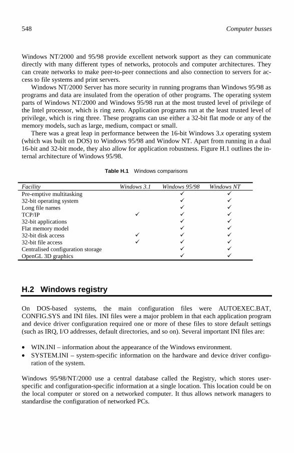
548 Computer busses
Windows NT/2000 and 95/98 provide excellent network support as they can communicate directly with many different types of networks, protocols and computer architectures. They can create networks to make peer-to-peer connections and also connection to servers for ac-cess to file systems and print servers. Windows NT/2000 Server has more security in running programs than Windows 95/98 as programs and data are insulated from the operation of other programs. The operating system parts of Windows NT/2000 and Windows 95/98 run at the most trusted level of privilege of the Intel processor, which is ring zero. Application programs run at the least trusted level of privilege, which is ring three. These programs can use either a 32-bit flat mode or any of the memory models, such as large, medium, compact or small. There was a great leap in performance between the 16-bit Windows 3.x operating system (which was built on DOS) to Windows 95/98 and Window NT. Apart from running in a dual 16-bit and 32-bit mode, they also allow for application robustness. Figure H.1 outlines the in-ternal architecture of Windows 95/98.
Table H.1 Windows comparisons
Facility Windows 3.1 Windows 95/98 Windows NT Pre-emptive multitasking 32-bit operating system Long file names TCP/IP 32-bit applications Flat memory model 32-bit disk access 32-bit file access Centralised configuration storage OpenGL 3D graphics
H.2 Windows registry
On DOS-based systems, the main configuration files were AUTOEXEC.BAT, CONFIG.SYS and INI files. INI files were a major problem in that each application program and device driver configuration required one or more of these files to store default settings (such as IRQ, I/O addresses, default directories, and so on). Several important INI files are: • WIN.INI – information about the appearance of the Windows environment. • SYSTEM.INI – system-specific information on the hardware and device driver configu-
ration of the system. Windows 95/98/NT/2000 use a central database called the Registry, which stores user-specific and configuration-specific information at a single location. This location could be on the local computer or stored on a networked computer. It thus allows network managers to standardise the configuration of networked PCs.

Microsoft Windows 549
Hardware
Device drivers
VirtualMachineManager
InstallableFilesystemManager
ConfigurationManager
Windows 95/98core
User interface tools (32-bit shell)
Applications
Registry
Figure H.1 Windows 95/98 architecture
When a computer is initially upgraded from Windows 3.x to Windows 95/98 the upgrade program reads the SYSTEM.INI file and system-specific information which it then puts into the Registry. Many INI files are still retained on the system as many Win16-based applica-tions use them. For example, Microsoft Word Version 6 uses the WINWORD6.INI to store package information, such as location of filters, location of spell checker, location of gram-mar checker, and so on. An example is
[Microsoft Word] WPHelp=0 USER-DOT-PATH=C:\MSOFFICE\WINWORD\TEMPLATE PICTURE-PATH=C:\MSOFFICE\WINWORD PROGRAMDIR=C:\MSOFFICE\WINWORD TOOLS-PATH=C:\MSOFFICE\WINWORD STARTUP-PATH=C:\DOCS\NOTES\ INI-PATH=C:\MSOFFICE\WINWORD DOC-PATH=C:\DOCS\NOTES\
An important role for the registry is to store hardware-specific information which can be used by hardware detection and plug-and-play programs. The configuration manager deter-mines the configuration of installed hardware (such as, IRQs, I/O addresses, and so on) and it uses this information to update the registry. This allows new devices to be installed and checked to see if they conflict with existing devices. If they are plug-and-play devices then the system assigns hardware parameters that do not conflict with existing devices. The advantages of the registry over INI files include: • No limit to size and data type – the Registry has no size restriction and can include binary
and text values (INI files are text based and are limited to 64 KB). • Hierarchical information – the registry is hierarchically arranged, whereas INI files are
non-hierarchical and support only two levels of information. • Standardised set-up – the registry provides a standardized method of setting up programs,
whereas many INI files contain a whole host of switches and entries, and are complicated to configure.

550 Computer busses
• Support for user-specific information – the registry allows the storage of user-specific in-formation, using the Hkey_Users key. This allows each user of a specific computer (or a networked computer) to have their own user-specific information. INI files do not sup-port this.
• Remote administration and system policies – the registry can be used to remotely admin-ister and set system policies (which are stored as registry values). These can be downloaded from a central server each time a new user logs on.
Figure H.2 shows an example of the registry in Windows 95/98.
Figure H.2 Example registry
H.3 Device drivers
In Windows 3.x, device drivers were complex entities and were, in part, static and unchang-ing. Windows 95/98/NT now provide enhanced support for hardware devices and peripherals including disk devices. Windows NT will be discussed in Section H.10. Windows 95/98 uses a universal driver/mini-driver architecture that makes writing device-specific code much eas-ier. The universal driver provides for most of the code for a specific class of device (such as for printers or mice) and the mini-driver is a relatively small and simple driver that provides additional information for the hardware. The actual system interface to the hardware (or some software parts) is through a virtual device driver (VxD), which is a 32-bit, protected-mode driver. These keep track of the state of the device for each application and ensure that the device is in the correct state whenever an application continues. This allows for multitasking programming and also for multi-access for a single device. VxD files also support hardware emulation, such as in the case of the MS-DOS device driver, where any calls to the PC hardware can be handled by the device driver and not by the physical hardware. Typical VxD drivers are: EISA.VXD EISA bus driver ISAPNP.VXD ISA plug-and-play SERIAL.VXD Serial port LPTENUM.VXD Parallel port MSMOUSE.VXD MS Mouse PARALINK.VXD Parallel port PCI.VXD PCI QC117.VXD Tape backup IRCOMM.VXD Infra-red comms UNIMODEM.VXD Modem WSOCK.VXD WinSock LPT.VXD LPT

Microsoft Windows 551
VMM32.VXD Memory management JAVASUP.VXD JavaScript PPPMAC.VXD PPP connection NDIS.VXD NDIS NDIS2SUP.VXD NDIS 2.0 NETBEUI.VXD Net BEUI NWREDIR.VXD NetWare Redirect VNETBIOS.VXD Net BIOS WSIPX.VXD IPX WSHTCP.VXD TCP In Windows 95/98, VxD files are loaded dynamically and are thus only loaded when they are required, whereas in Windows 3.x they were loaded statically (and thus took up a lot of memory). In Window 3.x these virtual device drivers have a 386 file extension.
Hardware
Mini-driver Mini-driver
Universal driver
Operating system
Figure H.3 Device drivers
H.4 Configuration manager
A major drawback with Windows 3.x and DOS is that they did not automate PC configura-tion. For this purpose, Windows 95/98 has a configuration manager. The left-hand side of Figure H.4 shows how it integrates into the system and the right side of Figure H.4 shows an example device connection of a PC. Its aims are: • Determine, with the aid of several subcomponents, each bus and each device on the sys-
tem, and their configuration settings. This is used to ensure that each device has unique IRQs and I/O port addresses and that there are no conflicts with other devices. With plug-and-play, devices can be configured so that they do not conflict with other devices.
• Monitor the PC for any changes to the number of devices connected and also the device types. If it detects any changes then it manages the reconfiguration of the devices.
The operation is as follows: 1. The configuration manager communicates with each of the bus enumerators and asks
them to identify all the devices on the buses and their respective resource requirements. A bus enumerator is a driver that is responsible for creating a hardware tree, which is a hi-erarchical representation of all the buses and devices on a computer. Figure H.5 shows an example tree.

552 Computer busses
2. The bus enumerator locates and gathers information from either the device drivers or the BIOS services for that particular device type. For example, the CD-ROM bus enumerator calls the CD-ROM drivers to gather information.
3. Each of the drivers is then loaded and they wait for the configuration manager to assign their specific resources (such as IRQs, I/O addresses, and so on).
4. The configuration manager calls on resource arbitrators to allocate resources for each de-vice.
5. Resource arbitrators identify any devices which are conflicting and tries to resolve them. 6. The configuration manager informs all device drivers of their device configuration. This
process is repeated when the BIOS or one of the other bus enumerators informs the configuration manager about a system configuration change.
Registry
ConfigurationManager
Enumerator
Device Device
DevicedriverArbitrator
Bus
Figure H.4 Configuration manager and example connection of devices
H.5 Virtual machine manager (VMM)
The perfect environment for a program is to run on a stand-alone, dedicated computer, which does not have any interference from any other programs and can have access to any device when it wants. This is the concept of the virtual machine. In Windows 95/98 the virtual ma-chine manager (VMM) provides each application with the system resources when it needs them. It creates and maintains the virtual machine environments in which applications and system processes run (in Windows 3.x the VMM was called WIN386.EXE). The VMM is responsible for three areas: • Process scheduling – responsible for scheduling processes. It allows for multiple applica-
tions to run concurrently and also for providing system resources to the applications and other processes that run. This allows multiple applications and other processes to run concurrently, using either co-operative multitasking or pre-emptive multitasking.

Microsoft Windows 553
• Memory paging – Windows 95/98/NT uses a demand-paged virtual memory system, which is based on a flat, linear address space accessed using 32-bit addresses. The system allocates each process a unique virtual address space of 4 GB. The upper 2 GB is shared, while the lower 2 GB is private to the application. This virtual address space is divided into equal blocks (or pages).
• MS-DOS Mode support – provides support for MS-DOS-based applications which must have exclusive access to the hardware. When an MS-DOS-based application runs in this mode then no other applications or processes are allowed to compete for system re-sources. The application thus has sole access to the resources, as illustrated in Figure H.5.
VirtualMachineManager
VirtualMachineManager
Program 1
- Process scheduling- Memory paging- MS-DOS support
Program 3
Program 2
Programs have access toall the resources of the computer,as if they were the only program running
Creating virtualmemory (up to 2/4GB) DOS
programDOS
program
DOS emulator
Figure H.5 Virtual Machine Manager
Windows 95/98 has a single VMM (named System VMM) in which all system processes run. Win32-based and Win16-based applications run within this VMM. Each MS-DOS-based application runs in its own VM.
H.5.1 Process scheduling and multitasking
This allows multiple applications and other processes to run concurrently, using either co-operative multitasking or pre-emptive multitasking. In Windows 3.x, applications ran using co-operative multitasking. This method requires that applications check the message queue periodically and give up control of the system to other applications. Unfortunately, applica-tions that do not check the message queue at frequent intervals can effectively ‘hog’ the processor and prevent other applications from running. As this does not provide effective multi-processing, Windows 95/98/NT uses pre-emptive multitasking for Win32-based appli-cations (but also supports co-operative multitasking for computability reasons). Thus, the op-erating system takes direct control away from the application tasks. Win16 programs need to yield to other tasks in order to multitask properly, whereas Win32-based programs do not need to yield to share resources. This is because Win32-based applications (called processes) use multithreading, which provides for multi-processing. A thread in a program is a unit of code that can get a time slice from the operating system to

554 Computer busses
run concurrently with other code units. Each process consists of one or more execution threads that identify the code path flow as it is run on the operating system. A Win32-based application can have multiple threads for a given process. This enhances the running of an application by improving throughput and responsiveness. It allows processes for smooth background processing.
H.5.2 Memory paging
Windows 95/98/NT use a demand-paged virtual memory system, which is based on a flat, linear address space using 32-bit addresses. The system allocates each process a unique vir-tual address space of 4 GB (which should be enough for most applications). The upper 2 GB is shared, while the lower 2 GB is private to the application. This virtual address space di-vides into equal blocks (or pages), as illustrated in Figure H.6.
Systemaddressable
memory
Applicationaddressable
memory
0GB
2GB
4GB
Systemaddressable
memory
Applicationaddressable
memory
0GB
2GB
4GB
Application 1: Page 1
Application 2: Page 1
Application 1: Page 5
Application 1: Page 6
Application 2: Page 2
Free page: Page 1
Application 1: Page 4
Application 2: Page 3
Free page: Page 2
Application 2: Page 4
Application 1: Page 3
Free page: Page 4
Free page: Page 5
Application 1
Application 2
Virtualmapping tophysicalmemory
Physical memory
Figure H.6 Memory paging
Demand paging is a method by which code and data are moved in pages from physical memory to a temporary paging file on disk. When required, information is then paged back into physical memory. The functions of the memory pager are: • To map virtual addresses from the process’s address space to physical pages in memory.
This then hides the physical organisation of memory from the process’s threads and en-sures that the thread can access the required memory when required. It also stops other processes from writing to another memory location.
• To support a 16-bit segmented memory model for Windows 3.x and MS-DOS applica-tions. In this addressing scheme the addresses are made from a 16-bit segment address and a 16-bit offset address.

Microsoft Windows 555
Windows 95/98/NT use the full addressing capabilities of the 80x86/Pentium processors by supporting a flat, linear memory model for 32-bit operating system functionality and Win32-based applications. This linear addressing model simplifies the development process for ap-plication vendors, and removes the performance penalties of a segmented memory architec-ture.
H.6 Multiple file systems
Windows 95/98/NT supports a layered file system architecture that directly supports multiple file systems (such as FAT and CDFS). Windows 95/98/NT have great performance im-provements over Windows 3.x, for example: • Support for 32-bit protected-mode code when reading and writing information to and
from a file system. • Support for 32-bit dynamically allocated cache size. • Support for an open file system architecture to enhance future system support. Figure H.7 shows the file system architecture used by Windows 95/98. It has the following components: • IFS (installable file system) manager. This is the arbiter for the access to different file
system components. On MS-DOS and Windows 3.x it was provided by interrupt 21h. Un-fortunately, some add-on components did not run correctly and interfered with other in-stalled drivers. It also did not directly support multiple network redirections (the IFS manager can have an unlimited number of 32-bit redirectors).
• File system drivers. These provide support file systems, such as FAT-based disk de-vices, CD-ROM file systems and redirected network devices. They are ring 0 compo-nents, whereas Windows 3.x supported them through MS-DOS. The two enhanced file systems are: • 32-bit VFAT – the ‘legacy’ 16-bit FAT file system suffers from many problems, such
as the 8.3 file format. The 32-bit VFAT format is an enhanced form which works di-rectly in the protected mode, and thus provides smooth multitasking as it is re-entrant and multithreaded (a non re-entrant system does not allow an interrupt within an inter-rupt). It uses the VFAT.VXD driver and uses 32-bit code for all file accesses. Another advantage is that it provides for real-mode disk caching (VCACHE), where cache memory is automatically allocated or deallocated when it is required (in Windows 3.x this was provided by the SMARTDRV.EXE program).
• 32-bit CDFS – the 32-bit, protected-mode CDFS format (as defined in the ISO 9660 standard) gives improved CD-ROM access and support for a dynamic cache (in Win-dows 3.x the MSCDEX driver provided to access CD-ROMs).
• Block I/O subsystem. This is responsible for the actual physical access to the disk drive.
Its components are:
• Input/Output Supervisor (IOS) – this component provides for an interface between the

556 Computer busses
file systems and drivers. It is responsible for the queuing of file service requests and for routing the requests to the appropriate file system driver.
• Port driver – this component is a 32-bit, protected-mode driver that communicates with a specific IDE disk device. It implements the functionality of the SCSI manager and miniport driver.
• SCSI layer – this component is a 32-bit, protected-mode, universal driver model ar-chitecture for communicating with SCSI devices. It provides all the high-level SCSI functionality, and then uses a miniport driver to handle device-specific I/O calls.
• Miniport driver– in Windows 95/98 these miniport driver models are used to write device-specific code. The Windows 95/98 miniport driver is a 32-bit protected-mode code, and is binary-compatible with Windows NT miniport drivers.
I/O Supervisor
Other layers
Port driver
SCSI Layer
Miniport driver
VFAT CDFS File SystemComponent
Block I/O Subsystem
Installable File System Manager
Figure H.7 File system architecture
In Windows 95/98, the I/O Supervisor (IOS) is a VxD that controls and manages all pro-tected-mode file system and block device drivers. It loads and initialises protected-mode de-vice drivers and provides services needed for I/O operations. In Windows 3.x the I/O Super-visor was *BLOCKDEV. Other responsibilities of the IOS include: • Registering drivers. • Routing and queuing I/O requests, and sending asynchronous notifications to drivers as
needed. • Providing services that drivers can use to allocate memory and complete I/O requests. On Windows 95/98, the IOS stores port drivers, miniport and VxD drivers in the SYSTEM\IOSUBSYS directory. The PDR file extension identifies the port drivers, MPD identifies miniport drivers and VxD (or 386) identifies the VxD drivers. Other clients or vir-tual device drivers should be stored in other directories and explicitly loaded using device= entries in SYSTEM.INI. A sample listing of the IOSUBSYS directory is
Directory of C:\WINDOWS\SYSTEM\IOSUBSYS AIC78XX.MPD AMSINT.MPD APIX.VXD ATAPCHNG.VXD BIGMEM.DRV CDFS.VXD CDTSD.VXD CDVSD.VXD DISKTSD.VXD DISKVSD.VXD DRVSPACX.VXD ESDI_506.PDR HSFLOP.PDR NCRC710.MPD NCRC810.MPD NECATAPI.VXD RMM.PDR SCSI1HLP.VXD SCSIPORT.PDR VOLTRACK.VXD

Microsoft Windows 557
H.7 Core system components
The core of Windows 95/98 has three components: user, kernel, and GDI (graphical device interface), each of which has a pair of DLLs (one for 32-bit accesses; the other for 16-bit ac-cesses). The 16-bit DLLs (dynamic link libraries) allow for Win16 and MS-DOS computability. Figure H.8 shows that the lowest-level services provided by the Windows 95/98 kernel are implemented as 32-bit code. In Windows 95/98 the names of the files are GDI32.DLL, KERNEL32.DLL and USER32.DLL; these are contained in the \WINDOWS\SYSTEM di-rectory.
User
GDI
Windows 95/98 core
Kernel
Figure H.8 Core components
H.7.1 User
The user component provides input and output to and from the user interface. Input is from the keyboard, mouse, and any other input device and the output is to the user interface. It also manages interaction with the sound driver, timer, and communications ports. Win32 applications and Windows 95/98 use an asynchronous input model for system in-put. With this, devices have an associated interrupt handler (for example, the keyboard inter-rupts with IRQ1) which converts the interrupt into a message. This message is then sent to a raw input thread area, which then passes the message to the appropriate message queue. Each Win32 application can have its own message queue, whereas all Win16 applications share a common message queue.
H.7.2 Kernel The kernel provides for core operating system components including file I/O services, virtual memory management, task scheduling and exception handling, such as: • File I/O services. • Exceptions – these are events that occur as a program runs and calls additional software
which is outside of the normal flow of control. For example, if an application generates an exception, the Kernel is able to communicate that exception to the application to per-form the necessary functions to resolve the problem. A typical exception is caused by a divide-by-zero error in a mathematical calculation, an exception routine can be designed so that it handles the error and does not crash the program.
• Virtual memory management – this resolves import references and supports demand pag-ing for the application.
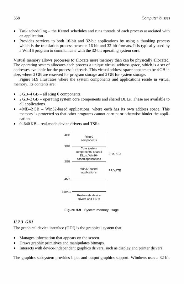
558 Computer busses
• Task scheduling – the Kernel schedules and runs threads of each process associated with an application.
• Provides services to both 16-bit and 32-bit applications by using a thunking process which is the translation process between 16-bit and 32-bit formats. It is typically used by a Win16 program to communicate with the 32-bit operating system core.
Virtual memory allows processes to allocate more memory than can be physically allocated. The operating system allocates each process a unique virtual address space, which is a set of addresses available for the process’s threads. This virtual address space appears to be 4 GB in size, where 2 GB are reserved for program storage and 2 GB for system storage. Figure H.9 illustrates where the system components and applications reside in virtual memory. Its contents are: • 3 GB–4 GB – all Ring 0 components. • 2 GB–3 GB – operating system core components and shared DLLs. These are available to
all applications. • 4 MB–2 GB – Win32-based applications, where each has its own address space. This
memory is protected so that other programs cannot corrupt or otherwise hinder the appli-cation.
• 0–640 KB – real-mode device drivers and TSRs.
Ring 0components
Win32-basedapplications
4MB
2GB
4GB
Core systemcomponents, shared
DLLs, Win16-based applications
3GB
Real-mode devicedrivers and TSRs
640KB
SHARED
PRIVATE
Figure H.9 System memory usage
H.7.3 GDI The graphical device interface (GDI) is the graphical system that: • Manages information that appears on the screen. • Draws graphic primitives and manipulates bitmaps. • Interacts with device-independent graphics drivers, such as display and printer drivers. The graphics subsystem provides input and output graphics support. Windows uses a 32-bit

Microsoft Windows 559
graphics engine (known as DIB, device-independent bitmaps) which: • Directly controls the graphics output on the screen. • Provides a set of optimized generic drawing functions for monochrome, 16-colour, 16-bit
high colour, 256-colour, and 24-bit true colour graphic devices. It also supports Bézier curves and paths.
• Support for image Colour Matching for better color matching between display and colour output devices.
The Windows graphics subsystem is included as a universal driver with a 32-bit mini-driver. The mini-driver provides only for the hardware-specific instructions. The 32-bit Windows 95/98 printing subsystem has several enhancements over Windows 3.x. These include: • They use a background thread processing to allow for smooth background printing. • Smooth printing where the operating system only passes data to the printer when it is
ready to receive more information. • They send enhanced metafile (EMF) format files, rather than raw printer data. This EMF
information is interpreted in the background and the results are then sent to the printer. • Support for deferred printing, where a print job can be sent to a printer and then stored
until the printer becomes available. • Support for bi-directional communication protocols for printers using the extended com-
munication port (ECP) printer communication standard. ECP mode allows printers to send messages to the user or to application programs. Typical messages are: ‘Paper Jam’, ‘Out-of-paper’, ‘Out-of-Memory’, ‘Toner Low’, and so on.
• Plug-and-play.
H.8 Multitasking and threading
Multitasking involves running several tasks at the same time. It normally involves running a process for a given amount of time, before releasing it and allowing another process a given amount of time. There are two forms of multitasking: • Pre-emptive multitasking – this involves the operating system controlling how long a
process stays on the processor. This allows for smooth multitasking and is used in Win-dows NT/95/98 32-bit programs.
• Co-operative multitasking – this relies on a process giving up the processor. It is used with Windows 3.x programs and suffers from processor hogging, where a process can stay on a processor and the operating system cannot kick it off.
The logical extension to multitasking programs is to split a program into a number a parts (threads) and run each of these on the multitasking system (multithreading). A program which is running more than one thread at a time is known as a multithreaded program. Multi-threaded programs have many advantages over non-multithreaded programs, including:

560 Computer busses
• They make better use of the processor, where different threads can be run when one or more threads are waiting for data. For example, a thread could be waiting for keyboard input, while another thread could be reading data from the disk.
• They are easier to test, as each thread can be tested independently of other threads. • They can use standard threads, which are optimised for given hardware. They also have disadvantages, including: • The program has to be planned properly so that threads know on which threads they de-
pend. • A thread may wait indefinitely for another thread which has crashed or terminated. The main difference between multiple processes and multiple threads is that each process has independent variables and data, while multiple threads share data from the main program.
H.8.1 Scheduling
Scheduling involves determining which thread should be run on the process at a given time. This element is named a time slice, and its actual value depends on the system configuration. Each thread currently running has a base priority. The programmer who created the pro-gram sets this base priority level of the thread. This value defines how the thread is executed in relation to other system threads. The thread with the highest priority gets use of the proc-essor. NT and 95/98 have 32 priority levels. The lowest priority is 0 and the highest is 31. A scheduler can change a threads base priority by increasing or decreasing it by two levels. This changes the threads priority. The scheduler is made up from two main parts: • Primary scheduler. This scheduler determines the priority numbers of the threads
which are currently running. It then compares their priority and assigns resources to them depending on their priority. Threads with the highest priority are executed for the current time slice. When two or more threads have the same priority then the threads are put on a stack. One thread is run and then put to the bottom of the stack, then the next is run and it is put to the bottom, and so on. This continues until all threads with the same priority have been run for a given time slice.
• Secondary scheduler. The primary scheduler runs threads with the highest priority, whereas the secondary scheduler is responsible for increasing the priority of non-executing threads (which are all other threads apart from the currently executed thread). It is thus important for giving low priority threads a chance to run on the operating sys-tem. Threads which are given a higher or lower priority are:
• A thread which is waiting for user input has its priority increased. • A thread that has completed a voluntary wait also has its priority increased. • Threads with a computation-bound thread get their priorities reduced. This prevents
the blocking of I/O operations.
Apart from these, all threads get a periodic increase. This prevents lower-priority threads hogging shared resources that are required by higher-priority threads.

Microsoft Windows 561
H.8.2 Priority inheritance boosting
One problem that can occur is when a low priority thread accesses resources which are re-quired by a higher priority thread. For example, an RS-232 program could be loading data into memory while another program requires to access the memory. One method which can be used to overcome this is priority inheritance boosting. In this case, low priority threads gets a boost so that they can quickly release resources. For example, suppose a system has three threads: Thread A, Thread B and Thread C. If Thread A has the highest priority and it requires a resource from Thread C then Thread C gets a boost in its priority. Thread A re-mains blocked until Thread C releases the required resource. When it does release it then Thread C goes back to its normal priority and Thread A then gets access to the resource.
H.9 Plug-and-play process
Plug-and-play allows the operating system to configure hardware as required. On system start-up, the configuration manager scans the system hardware. When it finds a new plug-and-play device it does the following: • Sets the device into configuration mode – this is achieved by using three I/O ports. Some
data (the initiation key) is written to one of the ports and enables the plug-and-play logic. • Isolate and identify each device – each device is isolated, one at a time. The method used
is to assign each device a unique number, which is a unique handle for the device. This number is made from a device ID and a serial number.
• Determine device specifications – each device sends its functionality to the operating system, such as how many joysticks it supports, its audio functions, its networking modes, and so on.
• Allocate resources – the operating system then allocates resources to the device depend-ing on its functionality and the plug-and-play device is informed of the allocated re-sources (such as IRQs, I/O addresses, DMA channels, and so on). It also checks for con-flicts on these resources.
• Activate device – when the above have been completed the device is enabled. Only the initiation key can re-initialise the device.
H.10 Windows NT architecture
Windows NT uses two modes: • User mode – this is a lower privileged mode than kernel mode. It has no direct access to
the hardware or to memory. It interfaces to the operating system through well-defined API (application program interface) calls.
• Kernel mode – this is a privileged mode of operation and allows all code direct access to the hardware and memory, including memory allocated to user mode processes. Kernel mode processes also have a higher priority over user mode processes.

562 Computer busses
Figure H.10 shows an outline of the architecture of NT. It can be seen that only the kernel mode has access to the hardware. This kernel includes executive services which include managers (for I/O, interprocess communications, and so on) and device drivers (which con-trol the hardware). Its parts include: • Microkernel – controls basic operating system services, such as interrupt handling and
scheduling. • HAL (hardware abstraction layer) – this is a library of hardware-specific programs
which give a standard interface between the hardware and software. This can either be Microsoft written or manufacturer provided. They have the advantage of allowing for transportability of programs across different hardware platforms.
• Win32 window manager – supports Win32, MS-DOS and Windows 3.x applications.
Hardware
Device driver
HAL (Hardware abstraction layer)
Microkernel
I/O manager
Object manager
Process manager
Local procedure
call facility
Virtual memory manager
Win32 window manager
Graphic device driver
Executive Services
NT Executive
Application
User mode Kernel mode
Figure H.10 NT architecture
H.10.1 MS-DOS support
Windows NT supports MS-DOS-based applications with an NT Virtual DOS Machine (NTVDM), where each MS-DOS application has its own NTVDM. The NTVDM is started by the application Ntvdm.exe and when this has started the application communicates with two system files Ntio.sys (equivalent to IO.SYS) and Ntdos.sys (equivalent to MSDOS.SYS). Note that the AUTOEXEC.BAT and CONFIG.SYS files have also been re-placed by Autoexec.nt and Config.nt (which are normally located in \WINNT\System32). Multiple NTVDMs have the advantage of being reliable because if one NTVDM fails then it does not affect any others. It also allows MS-DOS-based applications to be multi-tasked. Unfortunately, each NTVDM needs at least 1 MB of physical memory. Some MS-DOS applications require direct access to the hardware. NT supports this by

Microsoft Windows 563
providing virtual device drivers (VDDs). These detect a call to hardware and communicate with the NT 32-bit device driver. Windows NT communicates with hardware through device drivers. These drivers have a .sys file extension. An example listing of these is Directory of C:\WINNT\system32\drivers afd.sys atapi.sys atdisk.sys beep.sys cdaudio.sys cdfs.sys cdrom.sys changer.sys cirrus.sys disk.sys diskdump.sys diskperf.sys fastfat.sys floppy.sys ftdisk.sys hpscan16.sys i8042prt.sys kbdclass.sys ksecdd.sys modem.sys mouclass.sys msfs.sys mup.sys ndis.sys netdtect.sys npfs.sys ntfs.sys null.sys parallel.sys parport.sys parvdm.sys pcmcia.sys scsiport.sys scsiprnt.sys scsiscan.sys serial.sys sfloppy.sys streams.sys tape.sys tdi.sys vga.sys videoprt.sys
With this, virtual memory applications can have access to the full available memory but NT then maps this to a private memory range (called a virtual memory space). It maps physical memory to virtual memory in 4 KB blocks (called pages). This was previously illustrated in Figure H.6. The driver used to perform the page file access is Pagefile.sys (which is normally found in the top-level directory). Windows NT has 32 levels of priority (0 to 31). Levels 0 to 15 are used for dynamic ap-plications (such as non-critical operations) and 16 to 31 are used for real-time applications (such as Kernel operations). NT provides a virtual memory by paging file(s) onto the hard disk. Priority levels 0 to 15 can be paged, but levels 16 to 31 cannot. A summary of the system32 directory is shown below. The wowdeb.exe and wowexec.exe files allow Windows 3.x programs to run in a 32-bit environment. Directory of C:\winnt\system32 ansi.sys append.exe at.exe atsvc.exe attrib.exe autoexec.nt backup.exe bootok.exe bootvrfy.exe cacls.exe chcp.com chkdsk.exe clipsrv.exe comm.drv command.com comp.exe compact.exe config.nt control.exe convert.exe country.sys csrss.exe dcomcnfg.exe ddeshare.exe ddhelp.exe ebug.exe diskcomp.com diskcopy.com diskperf.exe doskey.exe dosx.exe DRIVERS edit.com exe2bin.exe expand.exe fastopen.exe fc.exe find.exe findstr.exe finger.exe fontview.exe forcedos.exe format.com ftp.exe gdi.exe graftabl.com graphics.com grpconv.exe help.exe himem.sys inetins.exe internat.exe kb16.com keyb.com keyboard.drv keyboard.sys krnl386.exe label.exe lights.exe lodctr.exe mem.exe mode.com more.com mpnotify.exe mscdexnt.exe nddeagnt.exe nddeapir.exe net.exe nlsfunc.exe notepad.exe ntdos.sys ntio.sys ntvdm.exe os2ss.exe pax.exe pentnt.exe ping.exe portuas.exe posix.exe print.exe psxss.exe rdisk.exe recover.exe redir.exe replace.exe restore.exe rpcss.exe rundll32.exe runonce.exe savedump.exe setup.exe setver.exe share.exe shmgrate.exe skeys.exe smss.exe sort.exe SPOOL sprestrt.exe subst.exe syncapp.exe sysedit.exe systray.exe taskman.exe
564 Computer busses
taskmgr.exe telnet.exe tree.com unlodctr.exe ups.exe user.exe userinit.exe VIEWERS win.com winhlp32.exe winspool.exe winver.exe wowdeb.exe wowexec.exe
H.11 Windows 95 and Windows 98
Windows 98 was really an upgrade to Windows 95 OSR2 (which includes NetMeeting, ScanDisk and Disk Defragmenter) and inherits many of the programs that were released with Windows 95 OSR2. The new features include: • Advanced plug and play. USB devices can be added to the computer without rebooting
it. • Automatic hardware detection. • Enhanced power management. • Increased WWW integration. WWW page creation, integrated email, channels, and so
on. • Windows updates. This facility allows for a single source to update system drivers, sys-
tem files and operating system programs, such as service packs. • System file checker. The facility checks for system files and recovers old system files. It
also checks the integrity of the operating system files and if necessary restores them or extracts them from the installation disks.
• Maintenance wizard. This facility allows tasks to be run at given time intervals. • Multiple monitors. The facility allows the computer to display to multiple monitors.
Different parts of the screen can be sent to the connected monitors, and thus expand the physical size of the desktop area.
• NetShow. The facility allows for the reception of streamed multimedia from a WWW server. It synchronises video, audio and graphics data.
• WWW TV. This facility combines broadcast TV and Internet-based content into a single program. With an Internet connection, television program listings are included giving lists of scheduled television shows. Broadcast TV requires a TV tuner card.
• Support for new devices. Windows 98 supports many new hardware devices, such as: universal serial bus (USB), IEEE 1394, accelerated graphics port (AGP) and DVD. IEEE 1394 defines a class of hardware that makes it easy to add serial devices to your computer. The AGP is an enhanced video card interface which give enhanced support for 3-D animation. DVD drives play software, videos and music CDs.
• Subscription. This facility allows Internet Explorer to check a WWW site for new con-tent, at given time intervals. This new content can be automatically downloaded (or prompted for a download).
• Channels. This facility allows content from WWW sites to be automatically down-loaded. It is similar to subscription, but the content provider can suggest a schedule for the subscription and it gives a rich map of the WWW site (rather than a single WWW page).

Microsoft Windows 565
H.12 Fundamentals of Operating Systems
H.12.1 Multitasking and threading
Multitasking involves running several tasks at the same time. It normally involves running a process for a given amount of time, before releasing it and allowing another process a given amount of time. The two forms of multitasking are illustrated in Figure H.11 and Figure H.13.
Processor Okay No.1, you’ve had your turn,
get to the back ofthe queue. Next!
Okay No.1, you’ve had your turn,
get to the back ofthe queue. Next! Process queue
23 4 5
1
Come on. My turn soon
Come on. My turn soon
Pre-emptive multitasking:Processes are given some time on the processor. This allows all the processes to have some time on the processor, and makes for smoother and more reliable operation
Figure H.11 Pre-emptive multitasking
Sorry. You’ll have towait until he’s
finished
Sorry. You’ll have towait until he’s
finished
6
Process queue
2 3 4 5
Processor
1
Hurry up. I’mwaiting. You’ve
been on that processorfor ages.
Hurry up. I’mwaiting. You’ve
been on that processorfor ages.
This isn’tvery fair!
This isn’tvery fair!
Hurray. I could stay here forever.
Anyway, I’m not going back to
the end of the queue.
Hurray. I could stay here forever.
Anyway, I’m not going back to
the end of the queue.
Co-operative multitasking:Processes must yield from the processor, before other processes can run on the processor
Sorry. You’ll have towait until he’s
finished
Sorry. You’ll have towait until he’s
finished
66
Process queue
2 3 4 5
Processor
1
Processor
1
Hurry up. I’mwaiting. You’ve
been on that processorfor ages.
Hurry up. I’mwaiting. You’ve
been on that processorfor ages.
This isn’tvery fair!
This isn’tvery fair!
Hurray. I could stay here forever.
Anyway, I’m not going back to
the end of the queue.
Hurray. I could stay here forever.
Anyway, I’m not going back to
the end of the queue.
Co-operative multitasking:Processes must yield from the processor, before other processes can run on the processor
Figure H.12 Co-operative multitasking

566 Computer busses
The two types are defined as: • Pre-emptive multitasking. This type of multitasking involves the operating system
controlling how long a process stays on the processor. This allows for smooth multitask-ing and is used in 32-bit Microsoft Windows programs and the UNIX operating system.
• Co-operative multitasking. This type of multitasking relies on a process giving up the processor. It is used with Windows 3.x programs and suffers from processor hogging, where a process can stay on a processor and the operating system cannot kick it off.
The logical extension to multitasking programs is to split a program into a number of parts (threads) and run each of these on the multitasking system (multithreading). A program that is running more than one thread at a time is known as a multithreaded program. Multi-threaded programs have many advantages over non-multithreaded programs, including: • They make better use of the processor, where different threads can be run when one or
more threads are waiting for data. For example, a thread could be waiting for keyboard input, while another thread could be reading data from the disk.
• They are easier to test, as each thread can be tested independently of other threads. • They can use standard threads, which are optimised for given hardware. They also have disadvantages, including: • The program has to be planned properly so that threads know on which other threads
they depend. • A thread may wait indefinitely for another thread which has crashed or terminated. The main difference between multiple processes and multiple threads is that each process has independent variables and data, while multiple threads share data from the main program, as illustrated in Figure H.13.
Threads
Process approach
Interlinkingof threads
Independentthreads
Threads approach
Process splits into threads
Process
Common sharingof data between threads
Figure H.13 Process splitting into threads

Microsoft Windows 567
H.13 Exercises
The following questions are multiple choice. Please select from a to d. H.13.1 Microsoft Windows 3.x in its standard form is: (a) An 8-bit operating system (b) A 16-bit operating system (c) A 32-bit operating system (d) A 64-bit operating system H.13.2 Microsoft Windows NT in its standard form is: (a) An 8-bit operating system (b) A 16-bit operating system (c) A 32-bit operating system (d) A 64-bit operating system H.13.3 How does the starting of Windows 95/98 differ from Windows 3.x? (a) An 8-bit operating system (b) A 16-bit operating system (c) Windows 3.x boots from DOS where as Windows 95/98 has its own boot procedure (d) A 64-bit operating system H.13.4 Where do 16-bit application programs get their configuration data? (a) INF files (b) INI files (c) BAT files (d) The system registry H.13.5 Where do 32-bit application programs get their configuration data? (a) INF files (b) INI files (c) BAT files (d) The system registry H.13.6 Which file is used to set up hardware? (a) SYSTEM.INI (b) WIN.INI (c) SETUP.INI (d) AUTOEXEC.INI H.13.7 Which files does Windows 3.x use for device drivers? (a) .386 (b) .VXD (c) .SYS (d) .DRV H.13.8 Which files does Windows 95/98 use for device drivers? (a) .386 (b) .VXD (c) .SYS (d) .DRV

568 Computer busses
H.13.9 Which files does Windows NT use for device drivers? (a) .386 (b) .VXD (c) .SYS (d) .DRV H.13.10 What is the 32-bit FAT disk format known as? (a) E-FAT (b) SFAT (c) Extended FAT (d) VFAT H.13.11 What the standard CD-ROM file system known as? (a) CDFS (b) CD-FAT (c) CD-RW (d) CD-R H.13.12 Which of the following best describes pre-emptive multitasking? (a) The operating system determines how long a process stays on the processor (b) Processes yield to other processes (c) Processes have a given time limit on the processor (d) Processes have sole access to the processor H.13.13 Which of the following best describes co-operative multitasking: (a) The operating system determines how long a process stays on the processor (b) Processes yield to other processes (c) Processes have a given time limit on the processor (d) Processes have sole access to the processor H.13.14 Discuss the advantages that the registry has over INI files. H.13.15 Discuss the architecture of the 32-bit Windows system. H.13.16 Discuss how Windows 95/98 use VxD device drivers to interface to the hardware.
How do equipment manufacturers develop drivers which use the VxD drivers? How do device drivers in NT differ from Windows 95/98?
H.13.17 Explain how the configuration manager is used to determine the devices which are
connected to the system. H.13.18 Explain the operation of the virtual machine manager. H.13.19 Explain the main differences between pre-emptive and co-operative multitasking.
Discuss also how multitasking and threading is implemented. H.13.20 Discuss how Windows 95/98 use priority systems to schedule processes.

HDLC
I.1 Introduction
The data link layer is the second layer in the OSI seven-layer model and its protocols define rules for the orderly exchange of data information between two adjacent nodes connected by a data link. Final framing, flow control between nodes, and error detection and correction are added at this layer. In previous chapters the data link layer was discussed in a practical man-ner. It is a use protocol as it provides a model for interfacing to a serial bus. The two types of protocol are: • Asynchronous protocol. • Synchronous protocol. Asynchronous communications uses start-stop method of communication where characters are sent between nodes, as illustrated in Figure I.1. Special characters are used to control the data flow. Typical flow control characters are End of Transmission (EOT), Acknowledge-ment (ACK), Start of Transmission (STX) and Negative Acknowledgement (NACK). Synchronous communications involves the transmission of frames of bits with start and end bit characters to delimit the frame. The two of the most popular are IBM’s synchronous data link communication (SDLC) and high-level data link control (HDLC). Many network data link layers are based upon these standards, examples include the LLC layer in IEE 802.x LAN standards and LAPB in the X.25 packet switching standard. Synchronous communications normally uses a bit-oriented protocol (BOP), where data is sent one bit at a time. The data link control information is interpreted on a bit-by-bit basis rather than with unique data link control characters.
END START
Synchronous
communications
Asynchronous
communications
10101011101001......01011101010
10101101 11100101 00101100 00000001 10101101 10001101
Figure I.1 Asynchronous and synchronous communications
I

570 Computer busses
HDLC is a standard developed by the ISO to provide a basis for the data link layer for point-to-point and multi-drop connections. It can transfer data either in a simplex, half-duplex, or full-duplex mode. Frames are generally limited to 256 bytes in length and a single control field performs most data link control functions.
I.2 HDLC protocol
In HDLC, a node is either defined as a primary station or a secondary station. A primary sta-tion controls the flow of information and issues commands to secondary stations. The secon-dary station then sends back responses to the primary. A primary station with one or more secondary stations is known as unbalanced configuration. HDLC allows for point-to-point and multi-drop. In point-to-point communications a pri-mary station communicates with a single secondary station. For multi-drop, one primary sta-tion communications with many secondary stations. In point-to-point communications it is possible for a station be operate as a primary and a secondary station. At any time, one of the stations can be a primary and the other the secon-dary. Thus, commands and responses flow back and forth over the transmission link. This is known as a balanced configuration, or combined stations.
I.2.1 HDLC modes of operation
HDLC has three modes of operation. Unbalanced configurations can use the normal response mode (NRM). Secondary stations can only transmit when specifically instructed by the pri-mary station. When used as a point-to-point or multi-drop configuration only one primary station is used. Figure I.2 shows a multi-drop NRM configuration. Unbalanced configurations can also use the asynchronous response mode (ARM). It dif-fers from NRM in that the secondary is allowed to communicate with the primary without receiving permission from the primary.
Secondarystation N
Secondarystation1
Primarystation
Commands
Responses
Primary/Secondarystation
Commands
Responses
Primary/Secondarystation
Normal responsemode (NRM)
Asynchronousbalancedmode (ABM)
Figure I.2 NRM and ABM mode
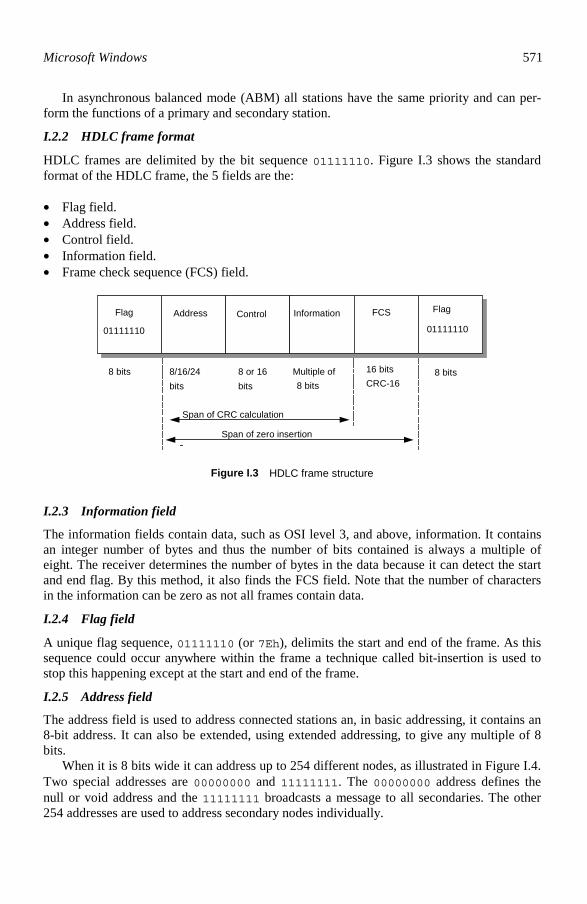
Microsoft Windows 571
In asynchronous balanced mode (ABM) all stations have the same priority and can per-form the functions of a primary and secondary station.
I.2.2 HDLC frame format
HDLC frames are delimited by the bit sequence 01111110. Figure I.3 shows the standard format of the HDLC frame, the 5 fields are the: • Flag field. • Address field. • Control field. • Information field. • Frame check sequence (FCS) field.
8 bits 8/16/24 bits
8 or 16bits
8 bits16 bitsCRC-16
Multiple of8 bits
Span of CRC calculation
Span of zero insertion
Flag Address Control Information FCS Flag
0111111001111110
Figure I.3 HDLC frame structure
I.2.3 Information field
The information fields contain data, such as OSI level 3, and above, information. It contains an integer number of bytes and thus the number of bits contained is always a multiple of eight. The receiver determines the number of bytes in the data because it can detect the start and end flag. By this method, it also finds the FCS field. Note that the number of characters in the information can be zero as not all frames contain data.
I.2.4 Flag field
A unique flag sequence, 01111110 (or 7Eh), delimits the start and end of the frame. As this sequence could occur anywhere within the frame a technique called bit-insertion is used to stop this happening except at the start and end of the frame.
I.2.5 Address field
The address field is used to address connected stations an, in basic addressing, it contains an 8-bit address. It can also be extended, using extended addressing, to give any multiple of 8 bits. When it is 8 bits wide it can address up to 254 different nodes, as illustrated in Figure I.4. Two special addresses are 00000000 and 11111111. The 00000000 address defines the null or void address and the 11111111 broadcasts a message to all secondaries. The other 254 addresses are used to address secondary nodes individually.
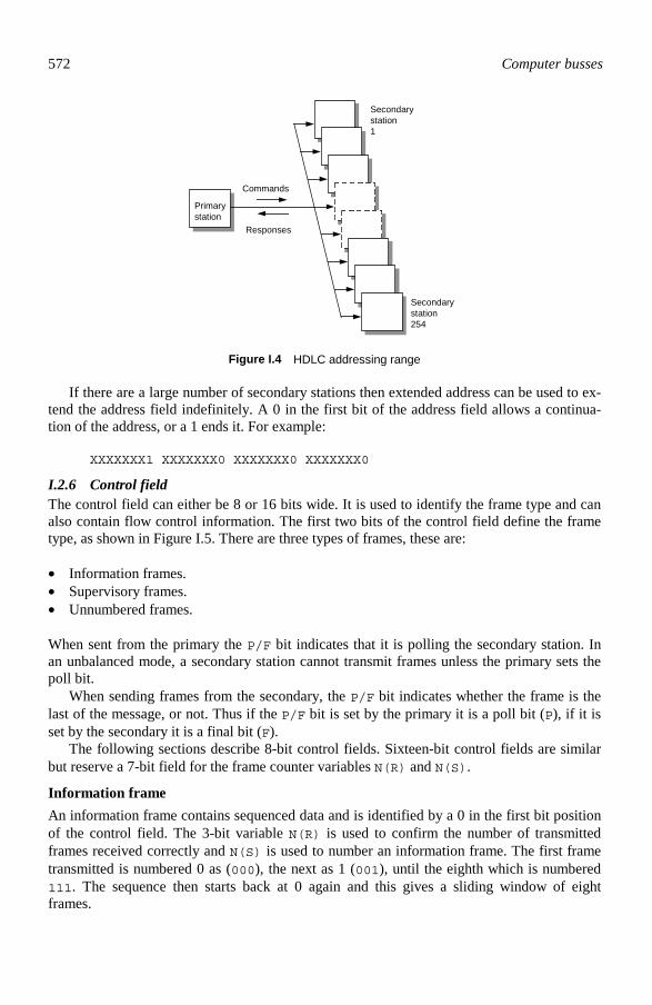
572 Computer busses
Primarystation
Secondarystation254
Secondarystation1
Commands
Responses
Figure I.4 HDLC addressing range
If there are a large number of secondary stations then extended address can be used to ex-tend the address field indefinitely. A 0 in the first bit of the address field allows a continua-tion of the address, or a 1 ends it. For example: XXXXXXX1 XXXXXXX0 XXXXXXX0 XXXXXXX0
I.2.6 Control field The control field can either be 8 or 16 bits wide. It is used to identify the frame type and can also contain flow control information. The first two bits of the control field define the frame type, as shown in Figure I.5. There are three types of frames, these are: • Information frames. • Supervisory frames. • Unnumbered frames. When sent from the primary the P/F bit indicates that it is polling the secondary station. In an unbalanced mode, a secondary station cannot transmit frames unless the primary sets the poll bit. When sending frames from the secondary, the P/F bit indicates whether the frame is the last of the message, or not. Thus if the P/F bit is set by the primary it is a poll bit (P), if it is set by the secondary it is a final bit (F). The following sections describe 8-bit control fields. Sixteen-bit control fields are similar but reserve a 7-bit field for the frame counter variables N(R) and N(S).
Information frame An information frame contains sequenced data and is identified by a 0 in the first bit position of the control field. The 3-bit variable N(R) is used to confirm the number of transmitted frames received correctly and N(S) is used to number an information frame. The first frame transmitted is numbered 0 as (000), the next as 1 (001), until the eighth which is numbered 111. The sequence then starts back at 0 again and this gives a sliding window of eight frames.

Microsoft Windows 573
0 Information frame
Supervisory frame
Unnumbered frame
Address Control Info FCS01111110 01111110
N(S) N(R)P/F
1 S N(R)P/F0
1 M MP/F1
b 7 b 6 b 5 b 4 b 3 b 2 b 1 b 0
Figure I.5 Format of an 8-bit control field
Supervisory frame
Supervisory frames contain flow control data. They confirm or reject previously received in-formation frames and also can indicate whether a station is ready to receive frames. The N(S) field is used with the S bits to acknowledge, or reject, previously transmitted frames. Responses from the receiver are set in the S field, these are receiver ready (RR), ready not to receive (RNR), reject (REJ) and selectively reject (SREJ). Table I.1 gives the format of these bits. RR informs the receiver that it acknowledges the frames sent up to N(R). RNR tells the transmitter that the receiver cannot receive any more frames at the present time (RR will can-cel this). It also acknowledges frames up to N(R). The REJ control rejects all frames after N(R). The transmitter must then send frames starting at N(R).
Table I.1 Supervisory bits
b5 b4 Receiver status 0 0 Receiver ready (RR) 1 0 Receiver not ready (RNR) 0 1 Reject (REJ) 1 1 Selectively reject (SREJ)
Unnumbered frame
If the first two bits of the control field are 1’s then it is an unnumbered frame. Apart from the P/F flag the other bits are used to send unnumbered commands. When sending commands, the P/F flag is a poll bit (asking for a response), and for responses it is a flag bit (end of re-sponse). The available commands are SARM (set asynchronous response mode), SNRM (set nor-mal response mode), SABM (set asynchronous balance mode), RSET (reset), FRMR (frame reject) and Disconnect (DISC). The available responses are UA (unnumbered acknowledge), CMDR (command reject), FRMR (frame reject) and DM (disconnect mode). Bit definitions for some of these are:

574 Computer busses
SABM 1111P110 DM 1111F000 DISC 1100P010 UA 1100F110 FRMR 1110F001
I.2.7 Frame check sequence field
The frame check sequence (FCS) field contains an error detection code based on cyclic re-dundancy check (CRC) polynomials. It is used to check the address, control and information fields, as previously illustrated in Figure I.2. HDLC uses a polynomial specified by CCITT V.41, which is 151216)( xxxxxG +++= . This is also known as CRC-16 or CRC-CCITT.
I.3 Transparency
The flag sequence 01111110 can occur anywhere in the frame. To prevent this a transpar-ency mechanism called zero-bit insertion or zero stuffing is used. There are two main rules that are applied, these are: • In the transmitter, a 0 is automatically inserted after five consecutive 1’s, except when the
flag occurs. • At the receiver, when five consecutive 1’s are received and the next bit is a 0 then the 0 is
deleted and removed. If it is a 1 then it must be a valid flag. In the following example a flag sequence appears in the data stream where it is not supposed to (spaces have been inserted around it). Notice that the transmitter detects five 1’s in a row and inserts a 0 to break them up. Message: 00111000101000 01111110 01011111 1111010101
Sent: 00111000101000 011111010 0101111101111010101
I.4 Flow control
Supervisory frames (S[]) send flow control information to acknowledge the reception of data frames or to reject frames. Unnumbered frames (U[]) set up the link between a primary and a secondary, by the primary sending commands and the secondary replying with re-sponses. Information frames (I[]) contain data.
I.4.1 Link connection
Figure I.6 shows how a primary station (node A) sets up a connection with a secondary sta-tion (node B) in NRM (normal response mode). In this mode one or many secondary stations can exist. First the primary station requests a link by sending an unnumbered frame with: node B’s address (ADDR_B), the set normal response mode (SNRM) command and with poll flag set (P=1), that is, U[SNRM,ABBR_B,P=1]. If the addressed secondary wishes to make a connection then it replies back with an unnumbered frame containing: its own address

Microsoft Windows 575
(ADDR_B), the unnumbered acknowledge (UA) response and the final bit set (F=1), i.e. U[UA,ABBR_B,F=1]. The secondary sends back its own address because many secondaries can exist and it thus identifies which station has responded. There is no need to send the pri-mary station address as only one primary exists. Once the link is set up data can flow between the nodes. To disconnect the link, the pri-mary station sends an unnumbered frame with: node B’s address (ADDR_B), the disconnect (DISC) command and the poll flag set (P=1), that is, U[DISC,ABBR_B,P=1]. If the ad-dressed secondary accepts the disconnection then it replies back with an unnumbered frame containing: its own address (ADDR_B), the unnumbered acknowledge (UA) response and the final bit set (F=1), i.e. U[UA,ABBR_B,F=1]. When two stations act as both primaries and secondaries then they use the asynchronous balanced mode (ABM). Each station has the same priority and can perform the functions of a primary and secondary station. Figure I.7 shows a typical connection. The ABM mode is set up initially using the SABM command (U[SABM,ABBR_B,P=1]). The connection between node A and node B is then similar to the NRM but, as node B operates as a primary station, it can send a disconnect command to node A (U[DISC,ABBR_B,P=1]). The SABM, SARM and SNRM modes set up communications using an 8-bit control field. Three other commands exist which set up a 16-bit control field, these are SABME (set asynchronous balanced mode extended), SARME and SNRME. The format of the 16-bit control field is given in Figure I.8.
U[SNRM,ADDR_B,P=1]
U[UA,ADDR_B,F=1]
U[DISC,ADDR_B,P=1]
U[UA,ADDR_B,F=1]
Node A Node B
Data flow
A B
Primary Secondary
Primary Secondary
Figure I.6 Connection between a primary and secondary in NRM
U[SABM,ADDR_B,P=1]
U[UA,ADDR_B,F=
1]
U[DISC,ADDR_B,
P=1]
U[UA,ADDR_A,F=1]
Node A Node B
Data flow
A B
Primary/Secondary
Primary/Secondary
Primary/Secondary
Primary/Secondary
Figure I.7 Connection between a primary/secondary in SABM

576 Computer busses
0 Information frame
Supervisory frame
Unnumbered frame
Address Control Info FCS01111110 01111110
N(S) N(R)P/F
1 S N(R)P/F0
1 M -P/F1 M
P/F
-
16 bits
Figure I.8 Extended control field.
Figure I.9 shows an example conversation between a sending station (node A) and a re-ceiving station (node B). Initially three information frames are sent numbered 2, 3 and 4 (I[N(S)=2], I[N(S)=3] and I[N(S)=4, P=1]). The last of these frames has the poll bit set, which indicates to node B that node A wishes it to respond, either to acknowledge or re-ject previously unacknowledged frames. Node B does this by sending back a supervisory frame (S[RR, N(R)=5]) with the receiver ready (RR) acknowledgement. This informs node A that node B expects to receive frame number 5 next. Thus it has acknowledged all frames up to and including frame 4. In the example in Figure I.9 an error has occurred in the reception of frame 5. The recipi-ent informs the sender by sending a supervisory frame with a reject flow command (S[REJ, N(R)=5]). After the sender receives this it resends each frame after and including frame 5. If the receiver does not want to communicate, at the present, it sends a receiver not ready flow command. For example S[RNR, N(R)=5] tells the transmitter to stop sending data, at the present. It also informs the sender that all frames up to frame 5 have been accepted. The sender will transmit frames once it has received a receiver ready frame from the receiver. Figure I.9 shows an example of data flow in only the one direction. With ABM both sta-tions can transmit and receive data. Thus each frame sent contains receive and send counter values. When stations send information frames the previously received frames can be ac-knowledged, or rejected, by piggy-backing the receive counter value. In Figure I.10, node A sends three information frames with I[N(S)=0,N(R)=0], I[N(S)=1, N(R)=0], and I[N(S)=2,N(R)=0]. The last frame informs node B that node A expects to receive frame 0 next. Node B then sends frame 0 and acknowledges the reception of all frames up to, and in-cluding frame 2 with I[N(S)=0,N(R)=3], and so on.
I.5 Derivatives of HDLC
There are many derivatives of HDLC, including:

Microsoft Windows 577
• LAPB (link access procedure balanced) is used in X.25 packet switched networks; • LAPM (link access procedure for modems) is used in error correction modems; • LLC (logical link control) is used in Ethernet and Token Ring networks; • LAPD (link access procedure D-channel) is used in Integrated Services Digital Networks
(ISDNs).
Node A Node B
I[N(S)=4,P=1]
S[RR,N(R)=5]
I[N(S)=2]
I[N(S)=3]
I[N(S)=5]
I[N(S)=6]
S[REJ,N(R)=5,F
=1]
I[N(S)=5]
I[N(S)=6]
Error in reception
Figure I.9 Example flow
Node A Node B
I[N(S)=2,N(R)=0]
I[N(S)=0,N(R)=
3]
I[N(S)=0,N(R)=0]I[N(S)=1,N(R)=0]
I[N(S)=3,N(R)=1]I[N(S)=4,N(R)=1]
I[N(S)=1,N(R)=
5]
I[N(S)=5,N(R)=2]I[N(S)=6,N(R)=2]
Acknowledgementup to and includingframe 2
Acknowledgementup to and includingframe 1
Acknowledgementup to and includingframe 4
0
1
2
3
4
5
6
0
1
Figure I.10 Example flow with piggy-backed acknowledgement

Example WinSock Code for Visual Basic
J.1 My client (myClient.frm)
VERSION 5.00 Object = "248DD890-BB45-11CF-9ABC-0080C7E7B78D#1.0#0"; "mswinsck.ocx" Begin VB.Form myClient Caption = "Client Application" ClientHeight = 3210 ClientLeft = 2250 ClientTop = 6195 ClientWidth = 8265 LinkTopic = "Form1" MaxButton = 0 'False ScaleHeight = 3210 ScaleWidth = 8265 StartUpPosition = 1 'CenterOwner Begin VB.CommandButton HelpClient Caption = "Example" Height = 375 Left = 4800 TabIndex = 15 Top = 2640 Width = 1335 End Begin VB.ListBox PortNameC Height = 840 ItemData = "myClient.frx":0000 Left = 4560 List = "myClient.frx":0016 TabIndex = 1 Top = 1080 Width = 1815 End Begin VB.TextBox AddressPort Height = 285 IMEMode = 3 'DISABLE Left = 6480 TabIndex = 14 TabStop = 0 'False Text = "Port Number" Top = 1080 Width = 1575 End Begin VB.TextBox EOTClient Enabled = 0 'False Height = 195 Left = 0 TabIndex = 11
J

580 Computer busses
TabStop = 0 'False Text = " EOT " Top = 120 Visible = 0 'False Width = 150 End Begin VB.CommandButton CloseC Caption = "Finish" Height = 375 Left = 6480 TabIndex = 5 Top = 2640 Width = 1335 End Begin VB.ComboBox AddressIP Height = 315 ItemData = "myClient.frx":0050 Left = 4560 List = "myClient.frx":005D TabIndex = 0 Text = "IP or DNS" Top = 480 Width = 3495 End Begin VB.CommandButton cmdDisConnect Caption = "Disconnect" Height = 375 Left = 6480 TabIndex = 4 Top = 2160 Width = 1335 End Begin VB.CommandButton cmdConnect Caption = "Connect" Height = 375 Left = 4800 TabIndex = 2 Top = 2160 Width = 1335 End Begin VB.TextBox ShowText Height = 1965 Left = 240 Locked = -1 'True MultiLine = -1 'True ScrollBars = 2 'Vertical TabIndex = 6 TabStop = 0 'False Top = 1080 Width = 3975 End Begin VB.TextBox SendTextData Height = 285 Left = 240 MultiLine = -1 'True TabIndex = 3 Top = 480 Width = 3975 End Begin MSWinsockLib.Winsock myTCPClient Left = 7800 Top = 0

Microsoft Windows 581
_ExtentX = 741 _ExtentY = 741 _Version = 327681 End Begin VB.Label Label1 Caption = "PortName" Height = 255 Left = 4560 TabIndex = 13 Top = 840 Width = 735 End Begin VB.Label CopyRight1 Caption = "email_address" Enabled = 0 'False BeginProperty Font Name = "Times New Roman" Size = 8.25 Charset = 0 Weight = 400 Underline = 0 'False Italic = 0 'False Strikethrough = 0 'False EndProperty Height = 255 Left = 6360 TabIndex = 12 Top = 3000 Width = 1935 End Begin VB.Label Label4 Caption = "AddressPort" Height = 255 Left = 6480 TabIndex = 10 Top = 840 Width = 975 End Begin VB.Label Label3 Caption = "AddressIP" Height = 255 Left = 4560 TabIndex = 9 Top = 240 Width = 855 End Begin VB.Label ShowLabel Caption = "ShowText" Enabled = 0 'False Height = 255 Left = 240 TabIndex = 8 Top = 840 Width = 3495 End Begin VB.Label SendLabel Caption = "SendTextData" Height = 255 Left = 240 TabIndex = 7 Top = 240 Width = 3495
582 Computer busses
End End Attribute VB_Name = "myClient" Attribute VB_GlobalNameSpace = False Attribute VB_Creatable = False Attribute VB_PredeclaredId = True Attribute VB_Exposed = False 'Last modification: 15/11/99 Private Sub Form_Load() Unload ChoiceSC 'Close the main menu properly SendTextData.Enabled = False 'Initialisation SendLabel.Enabled = False cmdDisConnect.Enabled = False cmdConnect.Enabled = True AddressIP.Enabled = True AddressPort.Enabled = False End Sub Private Sub cmdConnect_Click() 'Connect to the server myTCPClient.Connect SendTextData.Enabled = True SendLabel.Enabled = True cmdConnect.Enabled = False cmdDisConnect.Enabled = True AddressIP.Enabled = False AddressPort.Enabled = False CloseC.Enabled = False PortNameC.Enabled = False End Sub Private Sub cmdDisConnect_Click() 'Disconnect from the server myTCPClient.Close SendTextData.Enabled = False SendLabel.Enabled = False cmdConnect.Enabled = True cmdDisConnect.Enabled = False AddressIP.Enabled = True CloseC.Enabled = True PortNameC.Enabled = True End Sub Private Sub PortNameC_Click() 'Choice of the port (name) If PortNameC.Text = "--Manual enter-- >" Then AddressPort.Enabled = True Else AddressPort.Enabled = False If PortNameC.Text = "Test" Then AddressPort.Text = "1001" If PortNameC.Text = "Echo" Then AddressPort.Text = "7" If PortNameC.Text = "Daytime" Then AddressPort.Text = "13" If PortNameC.Text = "FTP" Then AddressPort.Text = "21" If PortNameC.Text = "Telnet" Then AddressPort.Text = "23" If PortNameC.Text = "SMTP" Then AddressPort.Text = "25" End Sub Private Sub myTCPClient_DataArrival(ByVal bytesTotal As Long) 'Display incoming data Dim str1 As String, str2 As String, str As String 'declare old, new, to-tal data str1 = ShowText.Text 'old data
Microsoft Windows 583
myTCPClient.GetData str2 'incoming data (new data) str = str1 + str2 'total data to display ShowText.Text = str 'display to ShowText End Sub Private Sub AddressIP_Click() 'Choose IP Address myTCPClient.RemoteHost = AddressIP.Text End Sub Private Sub AddressIP_Change() 'Enter IP or DNS address myTCPClient.RemoteHost = AddressIP.Text End Sub Private Sub AddressPort_Change() 'Change port number directly in the AddressPort box (manually) myTCPClient.RemotePort = AddressPort.Text End Sub Private Sub CloseC_Click() 'Return to main menu ChoiceSC.Show End Sub Private Sub SendTextData_KeyPress(KeyAscii As Integer) 'When you press the ENTER key the contain of the top box is sent If KeyAscii = 13 Then myTCPClient.SendData SendTextData.Text SendTextData.Text = "" End If End Sub
J.2 My server (myServer.frm)
VERSION 5.00 Object = "248DD890-BB45-11CF-9ABC-0080C7E7B78D#1.0#0"; "mswinsck.ocx" Begin VB.Form myServer Caption = "Server Application" ClientHeight = 3810 ClientLeft = 60 ClientTop = 345 ClientWidth = 3840 LinkTopic = "Form1" MaxButton = 0 'False ScaleHeight = 3810 ScaleWidth = 3840 StartUpPosition = 1 'CenterOwner Begin VB.CommandButton DisConnect Caption = "Disconnect" Height = 375 Left = 240 TabIndex = 7 Top = 3120 Width = 1335 End Begin VB.TextBox ConnectionState

584 Computer busses
Height = 375 Left = 1800 Locked = -1 'True TabIndex = 5 TabStop = 0 'False Top = 2520 Width = 1695 End Begin VB.CommandButton CloseS Caption = "Finish" Height = 375 Left = 2280 TabIndex = 4 Top = 3120 Width = 1335 End Begin VB.TextBox ShowText Enabled = 0 'False Height = 650 Left = 120 MultiLine = -1 'True ScrollBars = 2 'Vertical TabIndex = 1 Top = 1440 Width = 3615 End Begin VB.TextBox SendTextData Height = 650 Left = 120 MultiLine = -1 'True ScrollBars = 2 'Vertical TabIndex = 0 Top = 480 Width = 3615 End Begin MSWinsockLib.Winsock myTCPServer Left = 240 Top = 3120 _ExtentX = 741 _ExtentY = 741 _Version = 327681 End Begin VB.Label CopyRight2 Caption = "[email protected]" Enabled = 0 'False BeginProperty Font Name = "Times New Roman" Size = 8.25 Charset = 0 Weight = 400 Underline = 0 'False Italic = 0 'False Strikethrough = 0 'False EndProperty Height = 255 Left = 1920 TabIndex = 8 Top = 3600 Width = 1815 End Begin VB.Label Label3 Caption = "Connection State:"

Microsoft Windows 585
Height = 375 Left = 120 TabIndex = 6 Top = 2520 Width = 1575 End Begin VB.Label Label2 Caption = "ShowText" Height = 255 Left = 120 TabIndex = 3 Top = 1200 Width = 3615 End Begin VB.Label Label1 Caption = "SendTextData" Height = 255 Left = 120 TabIndex = 2 Top = 240 Width = 3615 End End Attribute VB_Name = "myServer" Attribute VB_GlobalNameSpace = False Attribute VB_Creatable = False Attribute VB_PredeclaredId = True Attribute VB_Exposed = False 'Last modification: 15/11/99 Private Sub Form_Load() Unload ChoiceSC 'Close main menu properly 'Set the local port to 1001 and listen for a connection myTCPServer.LocalPort = 1001 myTCPServer.Listen ConnectionState.Text = "Disconnected" DisConnect.Enabled = False End Sub Private Sub myTCPServer_Close() 'Close method myTCPServer.Close ConnectionState.Text = "Disconnected" SendTextData.Enabled = False End Sub Private Sub myTCPServer_ConnectionRequest(ByVal requestID As Long) 'Check state of socket, if it is not closed then close it. If myTCPServer.State <> sckClosed Then myTCPServer.Close 'Accept the request with the requestID parameter. myTCPServer.Accept requestID ConnectionState.Text = "Connected" DisConnect.Enabled = True CloseS.Enabled = False SendTextData.Enabled = True End Sub Private Sub SendTextData_Change() 'SendTextData contains the data to be sent 'This data is sent using the SendData method myTCPServer.SendData SendTextData.Text End Sub

586 Computer busses
Private Sub myTCPServer_DataArrival(ByVal bytesTotal As Long) 'Read incoming data into the str variable, 'then display it to ShowText Dim str As String myTCPServer.GetData str ShowText.Text = str End Sub Private Sub CloseS_Click() 'Return to main menu ChoiceSC.Show End Sub Private Sub DisConnect_Click() myTCPServer.Close ConnectionState.Text = "Disconnected" CloseS.Enabled = True DisConnect.Enabled = False End Sub
J.3 Choice form (ChoiceSC.frm)
VERSION 5.00 Begin VB.Form ChoiceSC Caption = "Server or Client?" ClientHeight = 1530 ClientLeft = 60 ClientTop = 345 ClientWidth = 4125 LinkTopic = "Form1" MaxButton = 0 'False Moveable = 0 'False ScaleHeight = 1530 ScaleWidth = 4125 StartUpPosition = 1 'CenterOwner Begin VB.CommandButton Client1 Caption = "Client" Height = 375 Left = 2160 TabIndex = 2 Top = 720 Width = 1215 End Begin VB.CommandButton Server1 Caption = "Server" Height = 375 Left = 840 TabIndex = 1 Top = 720 Width = 1215 End Begin VB.Label CopyRight0 Caption = "email_address" Enabled = 0 'False BeginProperty Font Name = "Times New Roman"

Microsoft Windows 587
Size = 8.25 Charset = 0 Weight = 400 Underline = 0 'False Italic = 0 'False Strikethrough = 0 'False EndProperty Height = 255 Left = 2160 TabIndex = 3 Top = 1320 Width = 1815 End Begin VB.Label Question1 Caption = "Which mode do you want to use?" Height = 375 Left = 840 TabIndex = 0 Top = 240 Width = 2535 End End Attribute VB_Name = "ChoiceSC" Attribute VB_GlobalNameSpace = False Attribute VB_Creatable = False Attribute VB_PredeclaredId = True Attribute VB_Exposed = False 'Last modification: 15/11/99 Private Sub Form_Load() Unload myClient 'Close Client form properly Unload myServer 'Close Server form properly End Sub Private Sub Server1_Click() Unload myClient 'Close Client form properly Unload myServer 'Close Server form properly myServer.Show End Sub Private Sub Client1_Click() Unload myClient 'Close Client form properly Unload myServer 'Close Server form properly myClient.Show End Sub
J.4 Error panel (ErrorPanel.frm)
VERSION 5.00 Begin VB.Form ErrorPanel BorderStyle = 4 'Fixed ToolWindow Caption = "00 Type Error" ClientHeight = 1545 ClientLeft = 45 ClientTop = 285 ClientWidth = 2385 LinkTopic = "Form1"
588 Computer busses
MaxButton = 0 'False MinButton = 0 'False Moveable = 0 'False NegotiateMenus = 0 'False ScaleHeight = 1545 ScaleWidth = 2385 ShowInTaskbar = 0 'False StartUpPosition = 1 'CenterOwner Begin VB.CommandButton OkButton Caption = "OK" Height = 375 Left = 960 TabIndex = 1 Top = 840 Width = 615 End Begin VB.Label CopyRight3 Caption = "email_address" BeginProperty Font Name = "Times New Roman" Size = 8.25 Charset = 0 Weight = 400 Underline = 0 'False Italic = 0 'False Strikethrough = 0 'False EndProperty Height = 255 Left = 600 TabIndex = 3 Top = 1320 Width = 1815 End Begin VB.Label ErrorLabel Caption = "Click OK to continue" Height = 255 Left = 480 TabIndex = 2 Top = 480 Width = 1575 End Begin VB.Label ErrorMessage Caption = "Error" BeginProperty Font Name = "System" Size = 9.75 Charset = 0 Weight = 700 Underline = 0 'False Italic = 0 'False Strikethrough = 0 'False EndProperty Height = 255 Left = 1080 TabIndex = 0 Top = 120 Width = 615 End End Attribute VB_Name = "ErrorPanel" Attribute VB_GlobalNameSpace = False Attribute VB_Creatable = False

Microsoft Windows 589
Attribute VB_PredeclaredId = True Attribute VB_Exposed = False 'Last modification 10/11/99 Private Sub Form_Load() ErrorPanel.Enabled = True ErrorPanel.Visible = True End Sub Private Sub OkButton_Click() ErrorPanel.Enabled = False ErrorPanel.Visible = False End Sub
J.5 Help form (help.frm)
VERSION 5.00 Begin VB.Form HELP BorderStyle = 4 'Fixed ToolWindow Caption = "Example - Help" ClientHeight = 3195 ClientLeft = 45 ClientTop = 285 ClientWidth = 4680 MaxButton = 0 'False MinButton = 0 'False ScaleHeight = 3195 ScaleWidth = 4680 ShowInTaskbar = 0 'False Begin VB.Label Copyright4 Caption = "email_address" BeginProperty Font Name = "Times New Roman" Size = 8.25 Charset = 0 Weight = 400 Underline = 0 'False Italic = 0 'False Strikethrough = 0 'False EndProperty Height = 255 Left = 2880 TabIndex = 0 Top = 2880 Width = 1695 End End Attribute VB_Name = "HELP" Attribute VB_GlobalNameSpace = False Attribute VB_Creatable = False Attribute VB_PredeclaredId = True Attribute VB_Exposed = False

Index
01111110, 311, 526, 538, 539, 541, 545,
571, 574 100BASE-FX, 446 100BASE-TX, 443, 445–451, 461 100Mbps, 42, 58, 60, 92, 109, 190, 342,
423, 430, 435, 445–453, 462, 463 100VG-AnyLAN, 445–451, 464 10BASE2, 427, 443, 444, 462, 463 10BASE5, 443, 444, 462, 463 10BASE-FL, 443 10BASE-T, 427, 443–446, 449, 463 10Mbps, 42, 58, 92–94, 124, 223, 247,
250, 284, 288, 342, 427, 435, 437, 442, 444–447, 450, 451, 453, 462, 464, 531
2000, 3, 5, 29, 30, 36, 70, 118, 198, 421, 489, 511, 514, 547, 548
28.8kbps, 253–255, 533 4004, 5, 6, 12, 39, 489 44.1kHz, 92–94, 156, 531, 545 64kbps, 531, 533–536, 538, 544–546 6502, 7–13, 16, 23, 29, 31, 39, 40, 42 6800, 7, 8, 10, 11, 12, 38, 39, 42 8008, 6, 7, 9, 12, 38, 39, 40, 476, 489 802.2, 439, 462, 463 802.3ab, 460 80286, 20–22, 25, 26, 31, 33, 35, 87, 97,
98, 489, 495, 502 80386, 21, 22, 25, 29, 33, 35, 43, 97, 98,
246, 489, 491, 494, 495, 498, 499, 502, 506, 507
80486, 26, 100, 105, 489, 490, 494, 495, 498, 499, 507
DX, 489, 495 pin out, 495
8080, 6–16, 25, 29, 39–43, 489, 506 8085, 6–8, 13, 489 8086, 13–21, 25, 26, 29, 30, 32, 38, 97,
117, 118, 243, 489–495, 501–503, 506
8088, 27 accumulator, 491
addressing registers, 492 connections, 491 count register, 146, 491 processor flags, 493 status registers, 492
82091AA, 121, 126, 133 8237, 123, 129, 133 82438, 121, 124 8250, 229, 233, 243 8B/10B, 459, 460 8B6T, 447 8mm video tape, 139, 154 A4 image, 267 AA, 260, 376, 527 AC, 42, 527, 536 ACK, 280, 328, 337, 338, 385–387, 392–
397, 525, 529, 542, 569 acknowledgement, 161, 290, 293, 327,
328, 338, 386, 387, 389, 391, 393, 394, 396, 399, 440, 490, 540, 576, 577
Acorn, 23, 24, 35 ADC, 291, 321 address bus, 6, 13, 26, 43, 49–55, 69, 70,
80, 81, 85–88, 92, 109, 119, 121, 173, 192, 215, 317, 489, 490, 494–496, 498, 503, 506, 509
address field, 182, 303, 304, 359, 360, 380, 428, 437, 442, 538, 539, 571, 572
addressable memory, 54, 87, 112, 173 addressing
implied, 493 ADPCM, 544 advanced power management, 131, 185 AGP, 49, 77, 95, 99, 119, 181, 203–215,
529–532, 564 graphics aperture, 214
AIP, 121, 126, 127, 133, 137 AIX, 28 algorithm, 266, 325, 339, 359, 428, 429,
458

592 Computer busses
Allen, Paul, 6, 7, 11, 37, 38, 39, 46 Alpha, 43, 44, 46, 47, 547 ALT, 514 AMD, 5, 12, 14, 21, 25, 26, 118, 456, 547 American, 1, 45, 118 American Constitution, 1 AMI, 535, 536, 545 amplitude modulation, 265, 461 amplitude-shift keying, 264 analogue, 133, 261, 267, 313, 316, 320,
321, 348, 349, 351, 465, 513–515, 534
animation, 564 ANSI, 10, 36, 51, 98, 143, 144, 187, 217,
218, 238, 345, 460, 461, 463, 525 API, 127, 399, 561 APIC, 121, 123, 503 Apple, 7–20, 23–26, 28–43, 83, 96, 97,
118, 156, 172 II, 7–19, 23, 24, 26, 28, 31, 32, 34,
39, 40, 42, 83 AppleTalk, 401, 416 application layer, 327, 334, 424 arp, 221, 373, 376, 383 ASCII, 3, 225–228, 230, 244, 254–256,
269, 302–306, 310–312, 482, 486, 524, 525, 527
BEL, 525 bit stream timings, 227 CR, 242, 258, 305, 521, 525 DC1, 229, 525 DC2, 525 DC3, 525 DC4, 229, 525 EOT, 525, 569 FF, 307, 308, 309, 310, 373, 376,
382, 383, 456, 525, 528 HT, 525 LF, 242, 305, 525 NUL, 525 SUB, 525 VT, 525
ASK, 264, 265 assembly, 14, 20, 40, 73–75, 358 AST, 98, 118 asynchronous, 91, 158, 188, 189, 190,
225, 227, 254, 255, 261, 348, 513, 540, 556, 557, 570, 571, 573, 575
asynchronous modem, 254
AT, 6, 20–22, 25, 28, 31, 33, 87, 97, 98, 144, 145, 256, 257, 259–263, 265, 268, 269, 446, 477, 511, 513
ATDT, 256, 257, 258, 259, 268 ATH, 256, 257, 258, 259 commands, 256, 269, 511 task file, 145
ATM, 101, 217, 218, 220, 221, 450, 451, 453, 458, 465, 521
attenuation, 58, 59, 60, 249, 426, 517 attributes, 13, 399, 420, 547 AU, 548, 562, 567 audio, 17, 24, 30, 79, 92, 94, 151–156,
174, 181, 190, 217, 218, 374, 505, 531, 544, 545, 561, 564
digital, 19, 151 automatic power control, 151 automatically answer, 253, 256 automatically dial, 253 backbone, 99, 222, 419, 420, 443, 445,
451, 459, 461, 463 backbone network, 459 balanced lines, 249 bandwidth, 57, 96, 181–183, 186, 188,
189, 204, 217–222, 253, 264, 268, 269, 315, 320, 343, 447, 451, 457, 458, 460, 461, 465, 543, 545
BASIC, 4–13, 16, 24, 30, 31, 32, 40, 46, 113, 114, 119
baud, 17, 219, 227, 228, 229, 236, 243, 244, 247, 254, 255, 265, 266, 268, 468, 469, 474–476, 477
rate, 218, 227, 228, 236, 243, 254, 255, 265, 476
BCC, 213 BCD, 286 bee-sting, 443 Bell, 1, 2, 6, 118, 255, 511, 514 BIOS, 15, 31, 62, 63, 66, 109, 110, 119,
136, 143, 149, 156, 183, 233, 273, 274, 298, 551, 552
BIOS printer, 273, 274 B-ISDN, 534 BIST, 111 Bit rate, 42, 58, 96, 99, 190, 217, 223,
227, 241, 246, 249, 251, 254, 255, 265, 266–268, 287, 330, 333, 342, 343, 423, 426, 427, 429, 430–435, 441, 445–447, 450, 460–463, 468,

Table of contents 593
477, 532, 533, 536, 538, 543–546 bit shift, 339, 491 bit stuffing, 337, 339, 539, 545 BITBUS, 314 bit-mapped, 5, 16, 514, 515, 516 bitstream, 267, 442, 447, 448, 454, 536,
539, 541 bitwise, 10, 282, 333, 483
AND, 10, 179, 335, 337 OR, 10, 161, 162, 171, 179, 226,
276, 337, 519 Blue Book, 153 BNC, 51, 58, 427, 443, 444, 454, 463 bootp, 369, 416 Borland, 6, 31, 73–75, 148, 237, 280,
287, 479, 484 bps, 53, 54, 96, 227, 228, 241, 254–257,
260, 264, 265, 267, 268, 483, 511, 514–516
bridge, 41, 55, 77, 99, 104–112, 117, 119, 136, 137, 184, 187, 191, 201, 204, 212, 213, 221, 261, 263, 355, 356, 371, 372, 382, 419, 420, 426–428, 431, 433, 450, 451, 453, 460, 505
filtering rate, 427 forward rate, 427 source route, 428 source routing, 428 spanning tree, 382, 420, 427, 428
brightness, 267 Broadband ISDN, 534 BS, 525 bus arbitration, 109 bus enumerator, 551, 552 bus network, 421, 423, 431 bus network, 222, 423, 435 bus transactions, 205 Busicom, 4, 5 byte enable, 89, 94, 106, 107, 108, 495,
496, 498, 507 byte enable signals, 107, 495, 498 C/C++, 6, 116, 237, 479 C++, 28, 31, 45, 74, 75, 83, 148, 237,
246, 275, 415, 416, 479 cable, 57, 219
cat-3, 60, 61, 222, 445–447 cat-4, 60, 61, 445 cat-5, 60, 61, 222, 445, 446, 450,
460, 461
characteristics, 58 impedance, 444 multimode, 219 single-mode, 219 types, 57, 284, 429, 430, 431, 444
cabling, 321, 323, 424, 459, 460, 461 cache, 29, 77, 104, 111, 119, 121, 124–
126, 132, 134–137, 142, 201, 489, 495, 497, 499–507, 529, 555
architecture, 500 control register, 135 hit rate, 499 level-2, 76, 79, 119, 125, 135, 501 look-through, 500, 501 write-back, 500 write-through, 500
CAD, 326 calling party number, 542 CAN, 49, 50, 101, 314, 315, 323, 333–
339–343, 445, 525, 529 capacitance, 59 carriage return, 244, 256, 259, 273, 303,
311, 477 cartridge, 27, 153, 154, 503 CBS, 2 CCITT, 255, 260, 511, 519–521, 525,
533, 534, 535, 541, 545, 574 CD, 19, 30, 35, 51, 73, 77, 78, 83, 94, 95,
96, 100, 137, 139, 142, 143, 146, 150–157, 172, 173, 181, 190, 221, 260, 271, 288, 289, 294, 300, 377, 420, 432, 435, 436, 442, 450, 451, 457, 458, 471–474, 528, 546, 547, 552, 555, 568
audio, 152 CD-DA, 151, 153 CD-E, 152, 153 CDFS, 547, 555, 556, 568 CD-I, 153 CD-R, 30, 35, 51, 73, 77, 78, 83,
94–96, 100, 137, 139, 142, 143, 146, 150–157, 172, 173, 181, 190, 221, 271, 288, 289, 294, 300, 377, 420, 432, 457, 546, 547, 552, 555, 568
CD-ROM, 30, 35, 51, 73, 77, 78, 83, 94, 95, 96, 100, 137, 139, 142, 143, 146, 150–157, 172, 173, 181, 190, 221, 271, 288, 289, 294, 377,

594 Computer busses
420, 432, 457, 546, 547, 552, 555, 568
CD-ROM-XA, 152, 153 CD-RW, 151, 568 disk format, 151 interfaces, 142 pit, 139, 150, 151
Centronics, 271, 272, 284, 289, 291, 299 CERN, 83 channel identification, 542 characteristic impedance, 58, 59, 60, 249,
442 cheapernet, 443, 462, 463 checksum, 387, 389 circuit-switched, 533, 534 CISC, 14 classes, 320, 364, 378, 388, 460 client, 5, 183, 184, 217, 221, 400, 409,
411, 412, 415, 416, 420, 432, 433, 451
client/server, 5, 217, 221, 415, 420, 432, 433
clock, 8, 12, 15, 20, 27, 29, 35, 44, 50–54, 65, 66, 78, 85, 86, 87, 91–94, 97, 103–106, 109, 110, 112, 119, 124, 129, 130–133, 136, 145, 171, 195, 197, 198, 204, 207, 210, 215, 225, 237, 254, 298, 325, 341, 348–350, 386, 395, 415, 437, 447, 454, 455, 456, 489, 490, 495, 496, 497, 501–503, 513, 530, 531
doubler, 489, 495 period, 53, 210 rates, 129
coaxial, 51, 58, 223, 423, 430, 431, 433, 435, 442, 454, 459, 462
COBOL, 3, 4, 10, 16, 83 codec, 79 codes
feedback, 232, 455 collision, 42, 315, 331, 435, 436, 438,
442, 445, 446, 453, 458, 464, 541 collision detection, 331, 435 collisions, 436 COM1, 63, 65–67, 73, 80, 96, 126, 130,
173, 191, 224, 229, 233, 237, 238, 242–244, 275, 469, 474, 475, 480, 482–484, 530
COM2, 63, 65–67, 73, 75, 76, 81, 96,
126, 130, 173, 178, 191, 224, 233, 242, 243, 244, 275, 476, 477, 482, 486, 530
Commodore, 7, 9, 11–13, 16–18, 23–25, 27, 29, 32, 34, 40, 42, 83, 97
PET, 7, 9, 11–13, 17, 23, 40, 83 compression ratio, 267, 268 concentrator, 421 configuration manager, 549, 551, 552,
568 connection-oriented, 222, 385 connectors, 51, 52, 58, 59, 77, 78, 92, 95,
97, 101, 137, 143, 157, 171, 186, 190, 191, 201, 218, 219, 224, 336, 435, 443, 449, 532
control field, 168, 327, 328, 330, 337, 439, 440, 441, 538, 539, 540, 570–573, 575, 576
control signals, 497 convolutional code
Trellis diagram, 266 core system components, 557 correction, 124, 255, 266, 415, 425, 461,
504, 512, 519, 569, 577 courier, 416 CP/M, 9–17, 19, 24, 27, 29, 40, 44 CPU, 12, 13, 20, 24, 27, 31, 131, 133,
183, 184, 204, 213, 348 CR, 258, 521 Cray Research, 12 CRC, 149, 183, 189, 303, 305, 306, 310,
312, 337–339, 436, 437, 458, 519–522, 541, 574
CRC-10, 521 CRC-12, 521 CRC-16, 519, 521, 574 CRC-32, 521 CRC-8, 521 CRC-CCITT, 519, 520, 521, 574 decoding example, 520
cross-talk, 51, 58–61 CRT, 18 CSMA, 316, 435, 436, 442, 450, 451, 458 CSMA/CD, 435, 436, 442, 450, 451, 458 CTS, 225, 229, 231–233, 242, 471–474,
512, 513, 516, 517, 529 cylinders, 141, 149, 150 DA, 129, 152, 305, 306, 528 DAC, 209, 210

Table of contents 595
DARPA, 355, 364 DAT, 139, 154, 327, 328, 387, 420 Data
buffer, 213 compression, 255, 300, 514, 517 computer-type, 154, 533 frame, 337, 338, 339, 356, 423, 424,
425, 426, 427, 440, 545, 574 link, 355 types, 318
data link layer, 326, 327, 331, 334, 355, 426, 436, 440, 441, 538, 569, 570
Data rate, 50, 250, 444 Data Register, 73, 74, 75 datastream-oriented, 385 date and time, 61, 64 dB, 58, 59, 60, 61 DB25S, 224 DB9S, 224 DC, 443, 447, 448, 454, 456, 528, 536,
537, 538 DC balancing, 536, 537 DCD, 512, 529 DCE, 224, 225, 232, 247, 512 D-channel contention, 541 DD, 129, 140, 528 DEC, 2–4, 7, 9, 12, 19, 23, 27, 28, 29, 37,
38, 40, 43, 44, 45, 46, 47, 83, 177, 382, 435
decimal, 286 Decimal, 525, 526, 527, 528 Delphi, 6, 31, 287 Demand Priority Access Method, 448 demand-paged, 553, 554 demodulator, 253 destination address, 188, 189, 328, 362,
380, 423, 435–438, 442, 492 device driver, 183, 547, 548, 550–552,
556, 558, 562, 563, 567, 568 DIB, 368, 559 dictionary, 319 dielectric, 58, 60 digital modulation, 264
ASK, 264, 265 FSK, 264, 265 PSK, 264, 265
Digital Research, 9, 11, 14, 15, 19, 27, 33, 40, 44
DIMM, 78, 132, 505
DIN plug, 191 DISC, 540, 573, 574, 575 disconnect mode, 540 discrete, 4, 288, 304, 307 disks
automatic defect reallocation, 158 capacity, 140, 149, 150 predictive failure analysis, 158
divide error, 63 division, 25, 31, 338, 339, 519, 522, 523 DM, 320, 540, 573, 574 DMA, 20, 73, 82, 85, 87, 89, 123, 129,
130, 132, 133, 145, 296, 348, 498, 530, 561
DNS, 368, 370, 376, 377, 411, 416 DOC, 549 domain names, 366, 367, 377, 433 DOS, 9, 14, 15, 16, 20, 24, 27, 28, 31,
33–45, 62, 63, 81, 100, 246, 275, 287, 479, 494, 547, 548, 550–557, 562, 567
DOS services, 63 DOS-based, 246, 479, 494, 548, 553, 562 DPSK, 265 DR, 19, 158 DRAM, 5, 49, 78, 79, 80, 104, 121, 124,
125, 128, 132, 134–137, 201, 204, 213, 499, 500, 504, 505, 507
DRAM interface, 128, 134 drive specifications, 142 DSR, 225, 229, 232, 242, 471–474, 513,
517, 529 DTE, 224, 225, 230, 232, 242, 247, 261,
512, 513 DTR, 225, 229, 232, 242, 260, 471, 472,
512, 529 D-type, 96, 191, 224, 254, 271, 284, 300,
443 ECC, 124, 149, 505 echo cancellation, 265, 266 ECP, 96, 133, 179, 271, 296–300, 358,
530, 531, 532, 559 EDO, 78, 128, 132, 134 EGB, 429 EIA, 51, 60, 223, 247, 249, 250, 267, 463 EIDE, 142–150, 155, 156, 531 EISA, 85, 91–94, 98, 103, 105, 111, 142,
155, 215, 220, 505, 531, 532, 550 electronic mail, 41, 42, 222, 287, 288,

596 Computer busses
378, 417, 425, 432, 433, 434, 564 electronic token, 423 EMF, 559 encryption, 343, 425 end delimiter, 326, 539 end of interrupt, 69, 280–283, 346, 348,
480, 482, 484 enhanced parallel port, 96, 133, 271, 289,
294–296, 299, 300, 531, 532 byte mode, 289, 293, 294 nibble mode, 289–293 protocol, 294 registers, 296
ENIAC, 1, 3, 36 ENQ, 525 EPROM, 5, 6, 80 error
control, 10, 226, 359, 440 detection, 124, 152, 171, 226, 266,
312, 315, 327, 337, 359, 425, 436, 437, 504, 519, 538, 541, 569, 574
Esc, 485 ESDI, 142, 155, 556 ETB, 525 ether, 370, 435, 442, 454 Ethernet, 5, 9, 19, 24, 35, 39, 42, 50–52,
83, 92–94, 100, 101, 109, 111, 119, 124, 246, 288, 300, 312, 313, 315, 325, 355, 356, 362, 370–376, 382, 419, 424, 425, 427, 435–465, 521, 531, 532, 577
100Mbps, 109, 445, 463 100BASE-4T, 446, 447, 464 100BASE-FX, 446 100BASE-T, 443, 445–451, 458,
461, 464 100BASE-TX, 443, 445, 446, 448,
449, 451, 461 100VG-AnyLAN, 443, 445, 446,
448–451, 464 10BASE2, 427, 443, 444, 450, 462,
463 10BASE5, 443, 444, 462, 463 10BASE-FL, 443, 462, 463 10BASE-T, 427, 443–446, 449, 458,
462, 463 10BASE-T connections, 447 AUI, 441 cheapernet, 443, 462, 463
DSAP, 439 fast ethernet, 190, 443, 445, 446,
448–450, 460, 461, 462, 464 implementation, 456 interframe gap, 458 LLC protocol, 440 MDI, 441 migration, 449 migration, 449 PLS, 441, 442 SNAP, 439, 463 SSAP, 439 thick-wire, 443, 444, 445, 462, 463 thinnet, 443, 444 thin-wite, 443, 444, 462, 463 transceiver, 442, 456, 459 types, 443
Ethernet II, 438 ETX, 525 exabyte, 154 exceptions, 557 Explorer, 428, 564 extended capability port, 96, 133, 179,
271, 296–300, 358, 530, 531, 532, 559
channel address, 296 forward data, 298 mode signals, 297
extended parallel port mode signals, 295 register definitions, 296
Fairchild, 2–5, 37, 44 Fast Ethernet, 190, 443, 445, 446, 448–
464 FAT, 555 fault tolerance, 19, 20 FAX, 255, 514
transmission, 267 Fax transmission, 267 FC, 218, 528 FCS, 327, 437, 440, 442, 541, 571, 574 FDDI, 101, 111, 220, 221, 355, 425, 427,
450, 451, 453, 458, 461, 521 attachments, 461 network, 111, 521
FF, 456 fiber optic, 446 fibre channel, 217–219, 222, 460, 532
standards, 218

Table of contents 597
fibre optic, 51, 52, 58, 219, 222, 269, 325, 331, 377, 423, 430, 432, 433, 435, 443, 459, 532
Fieldbus, 313–324 FOUNDATION, 313, 316–319 topology, 316 types, 313
FIFO, 133, 299, 304, 456 file system, 19, 27, 151–153, 547, 548,
555, 556, 568 FAT, 555, 568
FINGER, 387 Firewire, 181, 186–190, 529, 531, 532
packet format, 189 fixed disks, 141 floating-point, 490, 497, 502, 503 floppy disks, 140 flow control, 206, 217, 229, 249, 334,
440, 458, 512, 513, 516, 539, 541, 569, 572, 573, 574
flying head, 141 FORTRAN, 3, 4, 6, 10, 13, 16 fragment, 356, 358, 361 fragmentation, 361, 379, 380, 381, 382,
386 frame check sequence, 327, 437, 438,
538, 541, 571, 574 frame format, 225, 536 frame reject, 540 framing bits, 440, 535 frequency, 53, 54, 58, 60, 85, 93, 94, 104,
126, 129, 183, 198, 204, 236, 239, 240, 264, 265, 267, 351, 447, 454, 456, 461, 495, 544
Frequency-shift keying, 264, , 265 FRMR, 540, 573, 574 FTP, 356, 385–387, 392, 414, 416, 417,
563 full-duplex, 56, 264, 458, 460, 477, 570 G.711, 544 G.722, 544 G.728, 544 Games Port, 191 Gates, Bill, 6, 7, 9, 11, 13, 14, 23, 36, 37–
41, 46, 83 gateway, 36, 70, 118, 220, 355–362, 369–
371, 374, 377, 378, 380, 381, 382, 383, 388, 419, 420, 428
germanium, 1, 2
GIF, 253 Gigabit Ethernet Alliance, 457 gopher, 416 government, 1, 36 graphical device interface, 557, 558 graphical user interface, 27, 30, 31, 33,
40, 83, 92 gray scale, 267 green book, 153 ground, 224, 225, 233, 249, 271, 275,
300, 336, 342, 351, 454 group III, 267 group IV, 267 hackers, 417 HAL, 562 half-duplex, 56, 247, 248, 447, 458, 570 handshaking, 51, 52, 55–57, 80, 89, 90,
106, 108, 123, 164, 228–231, 232, 233, 237, 241, 242, 253, 271, 272, 290, 291, 293, 299, 346–348, 350, 352, 353, 415, 449, 467, 471, 472, 478, 512
hard-disk, 119, 146, 155, 156 hardware handshaking, 228, 231 Hayes, 17, 256, 269 hazards, 57, 430 HD, 32, 121, 140 HDLC, 569–571, 572, 574, 576 helix, 154 Hewlett-Packard, 4, 11, 18, 19, 32, 43,
98, 345 hexadecimal, 63, 302, 305, 306, 437, 494,
525 HFS, 152 hi-fi, 18, 151, 154, 545 Hollerith, 1, 36, 37 hosts, 356, 359, 362, 364, 366, 367, 371,
373–376, 378, 379, 385, 386, 388, 399, 408
HP, 4, 18, 28, 118, 382 HP-UX, 28 HTTP, 414, 416 hub, 59, 121, 124, 132, 181, 182, 184,
185, 217–221, 421, 436, 443–452, 460, 463, 532
Huffman, 267 coding, 267 modified, 267
Hz, 53, 54, 253, 264, 268, 512

598 Computer busses
I/O digital, 73 inputting a byte, 73 isolated, 70, 71 memory mapped, 69, 70 outputting a word, 75 port, 73, 74, 145, 191, 200, 242,
299, 451, 490, 497, 551, 561 read, 86, 107, 109, 174, 490 supervisor, 555, 556 write, 86, 107, 109, 174, 295, 490
IA5, 525 IBM, 1–47, 83, 87, 91, 97, 98, 101, 118,
271, 423, 489, 569 AT, 21, 25, 26, 35, 83, 97, 489 PC, 9, 13–16, 20–46, 83, 97, 98, 489
ICMP, 359, 360, 376–378, 381, 382, 385, 401
IDE, 51, 52, 73, 77, 78, 89, 95, 100, 104, 105, 111, 119, 121, 123, 129, 132, 133, 136, 137, 139, 142–149, 155–159, 172, 201, 215, 338, 529–532, 556
connections, 95, 143, 144 IDE0, 79, 95, 143 IDE1, 79, 95, 143 interface, 129, 132, 133, 142, 143,
145 ISA interface, 129
IEC, 60, 314, 345 IEEE, 271, 367, 375, 428, 435, 436, 437,
438, 439, 440, 441, 445, 446, 448, 457, 458, 459, 460, 462, 463, 564
802.3, 51, 435, 436, 437, 438, 439, 440, 441, 445, 446, 448, 457, 458, 459, 460, 462, 463
488, 101, 345, 346, 348, 352, 353, 529, 531, 532
802.2, 439, 462, 463 1284, 271, 289, 298 802.4, 462, 463 802.5, 448, 463 802.12, 446, 448 802.3u, 445, 446 802.3 frame format, 437 standards, 436
image scanner, 267 IMR, 68, 279, 281, 282, 283, 481, 482,
483, 484
inetd, 369 INF files, 567 initialisation, 283, 317, 318, 348, 386 installable file system, 555 Intel, 3–47, 76, 83, 85, 97–99, 104, 114,
117, 118, 121, 132, 185, 300, 314, 367, 435, 457, 489, 491, 499, 501–503, 505, 547, 548
interconnected networks, 356, 377, 420, 425, 427, 428, 432
interconnection length, 345, 426 interfacing, 70, 73
isolated, 70 memory, 70
internet, 218, 355, 356, 357, 358, 362, 363, 364, 365, 379–381, 425
Internet, 5, 6, 28, 41, 42, 77, 83, 190, 253, 269, 312, 343, 355–361, 365–368, 371, 374, 375, 377, 378–382, 385, 401, 402, 415, 416, 420, 427, 428, 432–435, 564
addresses, 362, 364, 380 datagram, 356, 357 example, 363 example domain addresses, 367 Explorer, 564 naming structure, 367 primary domain names, 367, 377 protocol, 355, 378
inter-networking, 355 interrupt, 61–65, 68, 69, 81, 82, 87, 89,
130, 183, 279, 281, 287, 431, 479, 482, 484, 493, 497
control port, 482 controller, 130 edge-triggered, 68 handling, 63–65 hardware, 61, 63, 64, 482 mask register, 68, 279, 281–283,
481–484 port, 68 processor, 62 request, 62–65, 68, 87, 89, 490, 497,
498 service routine, 61–66, 81, 282, 283,
483, 484 software, 61, 63 vector, 62, 65
interval timer, 130

Table of contents 599
IP, 36–41, 218, 221, 355–371, 373–380, 382, 383, 385–390, 399, 402, 408, 411, 413–417, 420, 425, 426, 431, 432, 433, 435, 439, 492, 548
address format, 362 address, 41, 355–357, 359, 360,
362–377, 380, 382, 385, 386, 402, 408, 411, 413–415, 420, 426, 431, 433
addressing, 356, 363, 364, 376 class A, 364, 366, 376, 377 class B, 364, 366, 377 class C, 364, 366 data frames, 356 data frames, 356 header, 359, 360, 362, 376, 378,
379, 385, 389, 390 header, 359, 360, 385 protocol, 356, 357, 359, 362, 439 time-to-live, 358, 359, 361, 362, 376 Version 6, 385
IPX, 382, 401, 416, 439, 551 IRQ, 62, 65–68, 82, 83, 112, 123, 156,
157, 229, 276, 280, 487, 509, 548 IRQ0, 62, 63, 65, 66, 68, 69, 80, 81,
87, 112, 124, 130 IRQ1, 62, 63, 65, 66, 69, 81, 82,
123, 124, 191, 195, 197, 198, 201, 557
IRQ10, 65, 87, 109, 123, 509 IRQ11, 65, 82, 123 IRQ12, 65, 89, 123, 124, 130, 198,
201 IRQ13, 65, 82, 89, 124, 130 IRQ14, 65, 87, 89, 123, 124, 130,
143, 144, 148, 509, 529 IRQ15, 65, 68, 81, 82, 89, 112, 123,
124, 130 IRQ2, 63, 65–69, 81, 87, 124, 130 IRQ3, 63, 65–69, 80, 81, 82, 123,
124, 126, 130, 201, 284, 487, 509 IRQ4, 63, 65–69, 81, 123, 126, 130,
201, 284, 481–484, 487 IRQ5, 63, 65–67, 82, 123, 126, 284 IRQ6, 63, 65, 67, 69, 123, 126 IRQ7, 63, 65–69, 81, 82, 87, 123,
124, 126, 130, 279, 280–284, 509 IRQ8, 65, 68, 123, 130 IRQ9, 65–67, 82, 89, 123, 124, 130,
509 ISA, 49, 50, 54, 78, 85–95, 97–105, 111,
117, 119, 121, 123, 124, 126, 129, 130, 132, 136, 137, 142, 143, 155, 171, 190, 191, 201, 215, 287, 295, 298, 316, 505, 509, 529, 531, 532, 550
IDE interface, 129 ISDN, 101, 253, 267, 269, 531–546
basic rate, 533–536, 546 B-channels, 534–541, 544, 546 B-ISDN, 534 broadband, 534 call clearing, 543 call establish, 543 channels, 534, 545 data link layer, 538 D-channel contention, 541 D-channel, 534, 536–538, 541, 544,
546, 577 frame format, 536, 537 H0, 511, 534 H11, 534, 535, 545 H12, 534, 535, 545 information messages, 543 network layer, 534, 541, 546 network messages, 543 physical layer, 534, 535 supervisory frame, 539, 546 system connections, 238, 536 TEI, 538, 539, 540, 542
ISO, 51, 60, 98, 151, 152, 188, 247, 333, 335, 341, 356, 416, 424, 536, 555, 570
ISO 9660, 151, 152, 555 ISO/IEC, 60, 188 isochronous, 181, 183, 188–190 ISO-IP, 356 Isolated I/O, 70, 71 Isolator, 454 ISR, 61–66, 282, 283, 483, 484 ITU, 247, 249, 250, 255, 265–267, 544,
545 jamming signal, 435 Java, 6, 28, 43, 246, 417, 469, 475 JavaScript, 551 Joliet, 152 JPEG, 253 keyboard, 63, 65, 66, 71, 96, 101, 133,

600 Computer busses
191, 195–197, 530 data ready, 66 interface, 195, 197, 198, 505
LAN, 58–60, 93, 313, 315, 419, 421, 428, 430, 432, 435, 436, 443, 451, 569
LAPD, 538, 541, 577 laser, 5, 6, 24, 32, 139, 150, 151, 219, 459 LCR, 233, 235–240, 243, 245, 482 LD-CELP, 544 least significant, 115, 116, 227, 276, 278,
483, 519 LED, 278 Lee De Forest, 36, 37 Lempel-Ziv, 266 lens, 150 library, 399, 562 light, 1, 51, 58, 150, 151, 219, 288, 310,
343, 430, 438 line break, 223 line driver, 249, 454 Link Access Procedure, 538 Linux, 28, 368, 369, 433 listeners, 188, 347, 353 LLC, 437, 439–442, 463, 569, 577
protocol, 440 local Area Network, 101 local bus, 85, 509, 530 logical block address, 147, 149, 167 logical link control, 577 logical unit number, 167 login, 42, 356, 378, 387, 416, 420, 425,
432, 433 loopback, 237, 261, 262, 263, 474, 486,
513–515 Lorenz, 1 Lotus, 13, 29, 33, 34, 35, 44, 83 LPT1, 65, 67, 73, 96, 126, 224, 274, 275,
280, 282, 530 LPT2, 65, 67, 73, 275 LRC, 303, 305–309, 311, 312, 523, 524 LRC/VRC, 523, 524 LSR, 233, 234, 235, 237, 238, 239, 240,
241, 243, 245, 481, 482, 485 Mac, 16, 20, 26, 28, 31, 32, 35, 42, 83,
96, 97 MAC, 111, 355, 356, 362, 369, 370, 427,
431, 435–437, 440–442, 453, 462, 463
address, 355, 356, 362, 369, 370,
426, 427, 431, 437, 440, 462 address, 355, 356, 362, 369, 370,
427, 440, 462 layer, 356, 436, 437, 441, 442, 453,
463 machine code, 70 magnetic disk, 139 magnetic fields, 139 magnetic tape, 139, 153, 154 magneto-optical, 152 Manchester
coding, 325, 330, 331, 443, 454–456, 464
decoder, 453, 454 M-ary, 265
ASK, 265 FSK, 265 modulation, 265 PSK, 265
math co-processor, 65 MAU, 442 media access control, 426, 435, 437, 441 memory, 5–10, 13, 14, 15, 16, 17, 21, 25–
30, 32, 33, 34, 40, 42, 43, 45, 46, 49, 50, 54, 55, 57, 62, 69–81, 85–89, 92, 94, 95, 99, 103, 104, 106, 107, 109, 111–115, 119, 121, 124, 125, 128, 131, 132, 134–137, 142, 148, 150, 164, 169, 173–179, 184, 188, 201, 203, 204, 210, 212, 214, 215, 228, 233, 269, 273, 275, 295, 298, 362, 395, 432, 451, 456, 489–509, 547, 548, 551, 553, 554–558, 561–563
addressing, 57, 493, 494, 499 map, 69, 71, 72, 73 mapped I/O, 70 mapped, 70 models, 548 paging, 553, 554 segmentation, 494 segmented, 13, 32, 43, 493, 494,
554, 555 metafile, 559 micro-ops, 503 microprocessor, 4–33, 38, 39, 49, 50, 70,
92, 93, 95, 97, 181, 320, 321, 489 Microsoft, 4, 6, 7, 9–47, 62, 70, 74, 75,
83, 97, 98, 100, 148, 190, 229, 237, 258, 287, 296, 300, 417, 420, 433,

Table of contents 601
495, 503, 547, 549, 562, 566, 567 Microsoft Windows, 6, 22, 27, 31, 33, 43,
44, 62, 70, 100, 229, 258, 287, 417, 433, 495, 503, 547, 566, 567
migration, 14, 446, 460, 461, 532 military, 21, 367 Miniport, 556 MIPs, 502 MIT, 33, 378 MITS, 7, 10–12, 83 MMX, 503, 505 MNP level 5, 265, 266 Modbus, 51, 301, 302, 303, 307, 309,
310, 311, 312 diagnostics, 309
Modem, 95, 96, 97, 100, 173, 181, 182, 227, 253, 254, 255, 256, 257, 260, 261, 264, 265, 266, 269, 477, 533, 534, 577
asynchronous, 254 AT commands, 256, 265 auto-answer, 253, 258, 260, 517 auto-dial, 253 commands, 256, 258, 259 connection, 199, 232, 237, 262, 263,
268, 355, 512 dialling, 259 example return codes, 257, 514 indicators, 260 profile viewing, 260 registers, 258, 517 return codes, 257 set-ups, 258 S-registers, 258, 269, 514 standards, 255 synchronous, 254 test modes, 261 typical, 265 V.22bis, 255, 265, 266, 511 V.32, 255, 265, 266, 511, 514 V.32bis, 255, 265, 266, 511, 514 V.42bis, 255, 265, 266, 514
modulator, 253 modulo-2, 338, 519, 522, 523 Moore, Gordon, 3, 4, 37, 38 MOS, 7, 8, 9, 11, 12, 39, 40, 100 MOS Technologies, 9 motherboard, 7, 12, 34, 77, 78, 100, 103–
105, 121, 124, 130, 132, 137, 142,
143, 156, 201, 206, 251, 269, 495, 507
430HX, 121, 131–134 MTXC, 132, 134, 136 TX, 3, 132, 249, 448, 450, 461, 465,
479, 529, 536 Motorola, 2, 7, 8, 10, 11, 12, 13, 16, 18,
20, 27, 32, 34, 36, 37, 38, 39, 40, 42, 97, 117, 118
mouse, 83, 96, 130, 191, 198, 199, 550 function, 130
MPEG, 151 MR, 260 MS-DOS, 11, 14, 24, 27, 28, 33, 36, 547,
550, 553–555, 557, 562 mode support, 553
MSX, 30, 44 multicast, 333, 374 multidrop, 218, 248, 316, 323, 423 multimedia, 375, 450 multiple file systems, 555 multiplexing, 106, 218, 271, 386, 534,
535 multiplexing/demultiplexing, 386 multi-station access unit, 442 multitasking, 34, 46, 486, 503, 547, 548,
550, 552–555, 559, 565, 566, 568 co-operative, 559, 565, 566 pre-emptive, 548, 559, 565, 566
multivibrator, 193 MUX, 129 NACK, 569 NAK, 310, 525 National Semiconductor, 12, 25, 29, 30,
32 NDIS, 551 NEC, 7, 15, 18, 30, 32, 38, 39, 40, 83, 98,
118, 367 Netscape, 83 netstat, 416 NetWare, 25, 28, 35, 83, 157, 421, 433,
439, 551 network, 26, 95, 218, 287, 322, 333, 355,
358, 364, 365, 372, 374, 375, 416, 421, 422, 425, 429, 433, 446, 449, 453, 454
addresses, 367, 538 cable types, 429 information center, 365

602 Computer busses
layer, 355, 357, 385, 425, 426, 428, 439, 463, 534, 541, 546
management, 342, 387, 449 topologies, 421, 422 traffic, 42, 321, 360, 433, 442
NFS RPC, 374
NIC, 365, 453 NIS, 374 NMI, 73, 124, 497, 498 noise, 50, 249, 264, 454, 461 non real-time, 448, 465 NRZ, 335, 337 nslookup, 368 NT, 22, 43, 70, 198, 421, 536, 537, 538,
541, 547, 548, 550, 553–556, 559–563, 567, 568
N-type, 443, 444, 463 object-oriented, 5, 28 OH, 260 operating system, 6, 9–11, 14–20, 22, 24,
26–28, 33, 34, 41–46, 61, 62, 76, 82, 83, 92, 119, 136, 153, 183, 184, 191, 195, 300, 397, 428, 433, 439, 502, 503, 547, 548, 553, 555, 557–562, 564, 566, 567, 568
operators, 285, 321 optical disks, 139, 150, 152 optical fibre, 186, 223, 325 optical storage, 150 opto-isolator, 251 OR, 276 Orange Book, 152, 153 OR-tied, 161, 171 OS/2, 22, 28, 41, 44, 157 Osborne, 7, 8, 23, 24, 29, 30, 83 OSF/1, 28 OSFP, 429 OSI, 331, 334, 335, 343, 355–357, 375,
385, 424, 425, 426, 436, 441, 463, 535, 569, 571
model, 335, 343, 355–357, 385, 424–426, 436, 441
PA, 314 packet, 152, 181–183, 188, 189, 199, 200,
315, 357, 359, 373, 386–388, 390–396, 415, 424, 426–428, 458, 546, 569, 577
PAL, 79, 134
palette, 133 PAM, 213, 461 parallel port, 49, 65, 66, 67, 73, 81, 96,
100, 121, 124, 126, 133, 190, 191, 201, 224, 246, 271, 275, 277, 279, 280, 282–284, 286–291, 294, 296, 298–300, 529–532, 550
byte mode, 289, 293, 294 Centronics, 271, 272, 284, 289, 291,
299 compatibility mode, 289, 290 enhanced, 96, 289 nibble mode, 289–293
PARC, 5, 9, 10, 16, 38 parity, 126, 158, 197, 226, 245, 303, 472,
474 even, 110, 226, 239, 240, 469, 493,
496, 523, 524 odd, 225, 226, 524
Pascal, 6, 10, 15, 24, 31, 39, 40, 73, 74, 75, 83, 235, 275
password, 133, 420, 421 PATH, 549 PC, 1, 4, 5, 9–36, 40–87, 91–100, 103–
105, 112, 118, 119, 128–132, 137, 142, 143, 156, 172, 178, 181, 182, 186, 187, 190, 191, 195, 215, 224, 232, 233, 246, 251, 269, 271, 272, 279, 287–290, 293, 298, 352, 368, 369, 486, 489, 490, 491, 494, 495, 499, 531, 532, 547, 548, 550, 551
bus, 49, 85, 86, 87, 93, 95, 96, 97, 100, 105
connectors, 224 PCI, 16, 49, 51, 77, 78, 85, 92–95, 98–
100, 103–132, 136, 137, 142, 155, 181, 184, 185, 190, 191, 201, 203–215, 220, 300, 345, 353, 504, 505, 530, 531, 532, 550
address phase, 108 AGP, 204, 215 bridge, 106–109, 112, 113, 117,
121, 181, 184, 201, 210–212, 504, 505
burst mode, 106, 108 bus cycles, 107 commands, 108 configuration address space, 110 configuration read access, 107, 109

Table of contents 603
configuration write access, 107, 109 dual addressing, 107, 109 interface, 204, 212 ISA bridge, 121, 123, 132 man. ID, 110, 118 multiple read, 107, 109 multiplexed mode, 106 operation, 106, 209 transfer modes, 106 unit ID, 110, 115
PCIset, 121, 122 PCM, 535, 536, 544, 545
delta modulation, 544 low-delay CELP, 544
PCMCIA, 85, 95, 99, 119, 137, 173–175, 178, 179, 287, 530, 531, 532
interface controller, 175 registers, 175 type II, 95, 173 type III, 95, 173 type IV, 95, 173
PCM-TDM, 535, 545 peer-to-peer, 315, 321, 420, 421, 431,
432, 433, 548 Pentium, 14, 21, 25, 42, 43, 78, 89, 104,
105, 109, 121, 122, 137, 288, 490, 491, 494, 495, 498, 499, 501–505, 507, 555
II, 121, 122, 490, 501–505 Pro, 501–504
permanent connection, 254, 534 phase shift keying, 264 phases, 162, 163, 164, 165, 171, 172,
266, 504 Philips, 19, 30, 151, 153 phone, 253, 256, 366 physical layer, 314, 325, 327, 331, 333–
335, 424–426, 441, 445, 446, 459, 460, 463, 534, 535
PIC, 63, 66, 68, 482 PIIX3, 121, 123, 124, 126, 127, 129–133,
136, 137, 184, 190, 530 PIIX4, 132, 133, 136, 184, 204 ping, 356, 359, 563 pipelined, 124, 135, 204, 206, 208, 209,
210, 502, 505 pixel, 33, 93, 131, 268 platter, 9, 141 PLL, 455, 456
plug-and-play, 99, 110, 118, 124, 181, 191, 549–551, 559, 561
pointer, 20, 149, 165, 213, 233, 361, 380, 381, 382, 387, 393, 398, 456, 492, 494
far, 233 near, 233
point-to-point protocol, 358, 551 polarisation, 150 poll/final bit, 539 polynomial, 306, 338, 339, 519–523, 541,
574 port driver, 556 port number, 386, 387, 389, 392, 401,
408, 414, 417, 468, 469, 476 ports and sockets, 386 power management, 121, 131, 136, 185,
207 power supplies, 537 PPI, 235 preamble, 326, 330, 437, 438, 440, 442,
443, 455, 463, 464 precedence, 386 pre-emptive, 547, 548, 552, 553, 554, 568 presentation, 319, 385, 424, 425 presentation layer, 424, 425 primary rate access, 534 print servers, 548 priority, 157, 160, 162, 171, 172, 181,
188, 205–207, 209, 213, 315, 319, 330, 333, 348, 358, 448, 450, 460, 560, 561, 563, 568, 571, 575
prism, 150 probability, 337 process scheduling, 552, 553 processor interrupts, 62 programmable interrupt controller, 63,
64, 66, 68, 280, 282, 482, 483, 530 prototyped, 73–75 PS, 22, 91, 96, 97, 101, 124, 130, 131,
137, 191, 197–199, 201, 532 PS/2, 22, 91, 96, 97, 101, 124, 130, 131,
137, 191, 197, 198, 199, 201, 532 PSK, 264, 265 PSTN, 517 PTC, 235 public telephone, 254, 356, 366, 534 pulse distortion, 249 pulse shaping, 461

604 Computer busses
QAM, 265 QIC, 154 QIC tapes, 154 QoS, 222, 460 QWERTY, 12 RADAR, 377, 432 Radio Shack, 7, 8, 12, 13, 17, 18, 23, 27,
30, 32, 34, 83 RAID, 221 RAM, 5, 7, 9, 11–13, 18, 19, 23, 24, 26,
27, 29–36, 49, 79, 93, 111, 121, 213, 456, 499, 513
RD, 225, 230, 233, 237–243, 260, 464 real-time, 101, 132, 133, 183, 188, 190,
217, 448, 460, 465, 486, 533, 534, 563
receiver not Ready, 441, 540 Receiver ready, 441, 540 Red Book, 152, 153 redundancy, 305, 337, 436, 437, 519,
523, 541, 574 reel-to-reel, 153 reflections, 58, 59 refresh rate, 135 registers, 73–75
general-purpose, 491 REJ, 441, 540, 573, 576 Reject, 441, 540, 573 repeater, 426, 427, 450, 451, 460, 463 requests, 206 resistance, 2, 58, 60, 98, 192, 193, 249,
430, 454 resolution, 24, 31, 32, 77, 93, 97, 103,
199, 203, 321, 323, 373 resource arbitrators, 552 RFC, 136, 382 RG-50, 443, 444 RG-6, 444 RGB, 131 RI, 474, 529 Ring
three, 548 zero, 548
ring in, 220, 221 ring network, 19, 111, 222, 355, 362, 421,
423, 431, 448, 577 ring out, 220, 221 RISC, 4, 9, 10, 14, 35, 36, 42, 44, 46 RJ-45, 51, 59, 427, 443, 444, 445, 448,
454, 463, 536 RLE, 267 RLE count, 297 RNR, 441, 540, 573, 576 ROM, 7, 9, 12, 13, 18, 23, 26, 27, 29–31,
49, 62, 73, 77, 79, 94, 96, 112, 139, 150, 152, 153, 271, 310, 505, 511, 552
ROM BIOS, 26, 62 routers, 374, 426, 428, 433 routing protocol
BGP, 428 EGP, 378, 428 OSPF, 429 RIP, 416, 429
RR, 441, 540, 573, 576 RS-232, 19, 51, 52, 96, 100, 101, 119,
195, 223–233, 237, 241–255, 269, 287, 300, 301, 312, 313, 345, 467, 468, 476, 477, 479, 482, 483, 523, 530, 531, 532, 561
485 converter, 250 bit stream timings, 227 communications, 224, 227, 232,
233, 242, 254, 477 DTE-DCE connections, 232 frame format, 225, 536 programming, 233 programs, 237 setup, 229
RS-328, 267 RS-422, 101, 223, 241, 246–251, 463 RS-422A, 247 RS-423, 247, 250 RS-449, 223, 247 RS-485, 247–251, 313, 314, 323, 335,
531, 532 RSVP, 460 RTS, 225, 229–233, 242, 249, 251, 471,
472, 512, 513, 516, 517, 529 RTU, 302, 303, 304, 305, 306, 312 run-length encoding, 267, 296, 297 SABME, 540, 575 sampling, 92–94, 199, 341, 543, 544 sampling rate, 92, 199, 544 SAPI, 538, 539, 542 scalability, 218, 446 SCSI, 36, 50–52, 77, 85, 96, 99, 100, 104,
111, 139, 142, 143, 156–172, 186,

Table of contents 605
191, 217, 218, 220, 221, 300, 345, 530, 531, 532, 556
A-cable, 158 arbitration, 162 B-cable, 158 commands, 162, 167 data, 162 fast/wide, 158 free-bus, 162 host, 159, 220 ID, 157, 160, 162, 172 III, 171 interface, 36, 139, 143, 159 layer, 556 logical unit number, 167 message codes, 165 message format, 165 message system description, 165 message, 163 operation, 162 P-cable, 158 pointers, 164 SCSI-I, 96, 142, 157–160, 162, 171,
172, 530, 531, 532 SCSI-II, 96, 142, 157–160, 171,
530, 531, 532 SCSI-III, 96, 157, 158 selection, 162 status, 163 tagged command queue, 157, 158
SD, 144, 260 Seagate Technologies, 17, 142 sectors, 139–141, 145, 146, 149–152 segment, 13, 42, 62, 212, 286, 327, 341,
355, 362, 373, 386–395, 426, 433, 435, 438, 443, 444, 446, 448, 450–453, 457, 460, 461, 464, 465, 492–494, 506, 554
sensor, 150, 319, 321 sequence number, 360, 361, 385–387,
390, 391, 393–396, 415, 441, 539 sequencing of data, 440 serial, 52, 53, 63, 65, 93, 96, 101, 129,
181, 190, 234, 237, 323, 529, 530, 550, 564
serial communications, 51, 85, 96, 223, 224, 233, 247, 275, 349, 467, 474, 479
server, 19, 44, 47, 128, 217, 221, 279,
366–370, 374, 385, 387, 392, 400, 403, 409, 410–423, 431–433, 449, 451, 453, 458, 460, 461, 547, 548, 550, 564
session layer, 425 set asynchronous balance mode extended, 540 seven-layer OSI model, 425 shielded twisted pair, 189, 222 signal-to-noise ratio, 461 silicon, 1, 2, 4, 15, 26, 30, 37, 103, 377,
432, 460 Silicon Graphics, 32, 36 SIMMs, 124, 128 simplex, 56 Sinclair, 7–9, 17, 18, 23–30, 40–42, 44 sine, 264 skin effect, 60 SMA, 443, 463 SMARTDRV.EXE, 555 SMTP, 28, 387, 414 SNMP, 28, 387, 416 SNR, 342 socket, 401, 402, 404, 406, 407, 408
number, 386 software handshaking, 229–231 software interrupts, 61, 63 Solaris, 28 Sony, 2, 7, 19, 26, 30, 99, 151, 367 sound, 27, 30, 40, 64, 66, 67, 78, 87, 92–
95, 119, 124, 137, 173, 557 source address, 328, 380, 423, 435, 436,
437, 438, 492, SPACE, 525 SPARC, 35, 42 speaker volume, 256, 511 speech, 99, 101, 188, 190, 253, 269, 448,
505, 533, 543, 544, 545 speech compression, 544 SPX, 401, 439
SPX/IPX, 401 SRAM, 49, 79, 80, 104, 121, 124, 129,
133–135, 137, 499, 507 SREJ, 573 ST connector, 443 ST-506, 142, 155 standalone, 267, 451 standards, 85, 95, 131, 153, 247, 424, 436 star network, 222, 421–423, 431, 446 start and end delimiter, 539

606 Computer busses
start bit, 195, 225, 226, 227, 254, 302, 303, 341
start delimiter, 326, 437 static, 5, 195, 550 stereo audio, 156 STM, 220, 221 stop bit, 195, 225–227, 229, 235, 239,
240, 254, 255, 302, 303, 468, 469, 474, 475, 476, 477, 483
STP, 58, 325, 430, 445 stream-oriented, 385 subnet, 355, 364–371, 374, 377, 378 subnet masks, 366 Sun Microsystems, 19, 23, 25, 26, 28, 35,
42, 83, 97, 246, 457 supervisory frames, 539, 572, 573, 574 switch, 43, 160, 174, 220, 221, 244, 245,
279, 343, 450–453, 458, 460, 461, 517
synchronisation, 341 synchronisation bits, 534, 536 synchronised, 254, 455, 456, 538 synchronous, 73, 91, 92, 124, 132, 157,
158, 195, 204, 254, 513, 569 synchronous modems, 254 syntax, 73–75 System Management Mode, 131, 136 system policies, 550 system reset, 498 system timer, 63, 65, 66, 530 System/360, 4, 7, 13, 21, 23, 36, 37 tab, 128 tape backup, 550 TCP, 28, 41, 51, 101, 217, 312, 343, 355–
362, 373, 375–378, 385–401, 408, 413–417, 420, 425, 432, 433, 435, 439, 548, 551
header format, 387, 388 Protocol Data Unit, 386
TCP/IP, 28, 36, 37, 39, 40, 41, 51, 101, 217, 312, 343, 355, 356, 358, 362, 375, 377, 385, 399, 416, 417, 420, 425, 433, 435, 439, 548
class A, 364, 366 class B, 364, 366 class C, 364, 366 gateway, 356, 362 implementation, 362 internets, 362
ports and sockets, 386 version number, 358
TD, 225, 230, 233, 237–243, 251, 464 TDI, 105, 110 TDM, 535, 545 TE, 536–538, 541, 542 TEI, 538, 539, 540, 542 telephone, 36, 41, 56, 58, 59, 187, 253,
254, 256–258, 262–264, 267–269, 355, 356, 366, 430, 513, 534, 538, 539, 543
telephone number, 257, 355, 356, 366, 513
teletex, 534 television, 564 telnet, 356, 385–387, 392, 414, 416, 425,
564 terminal, 87, 246, 258, 269, 480, 485 Texas Instruments, 2, 3, 5, 6, 9, 12, 13,
17, 19, 23, 25, 26, 29, 30, 37, 38, 271 thinnet, 443, 444 thin-wire, 462 throughput, 26, 80, 87, 92, 97, 98, 103,
116, 136, 171, 172, 190, 204, 215, 346, 358, 429, 446, 449, 531, 532, 554
ticker timer, 63 Time, 63 timestamp, 360, 361, 381, 382 Token Ring, 18, 35, 39, 220, 355, 356,
362, 371, 419, 423, 425, 448, 450, 453, 521, 577
MAUs, 442 topology, 51, 96, 181, 186, 187, 189,
220–222, 311, 315, 317, 323, 371, 372, 420–424, 433, 435, 446, 463
TR, 260 tracks, 139, 140 traffic, 42, 184, 188, 190, 191, 329, 330,
339, 360, 362, 378, 380, 382, 415, 419, 420, 422, 424, 427, 429, 432, 433, 435, 442, 445, 446, 451, 453–465, 533
transceiver, 335, 342, 442, 443, 444, 448, 453–456, 459, 500, 504
transfer length, 168 transfer rates, 152 transistor, 2–5, 37, 49, 79, 184, 288 transmission channel, 52, 264, 321

Table of contents 607
transmission line, 248, 249, 454 Transmission rates, 189 Transport, 355, 374, 375, 425 transport layer, 355–357, 385, 424, 425 tree topology, 422 trellis, 266 Turbo Pascal, 74, 275 twisted-pair, 51, 52, 58, 60, 182, 223,
269, 315, 316, 325, 333, 423, 426, 430, 433, 435, 442, 445–447, 459, 463, 532, 536
hubs, 445 TXC, 121, 124–127, 129, 132, 134, 136,
137, 201, 530 TX-O, 3 UDP, 383, 385, 389, 390, 401, 408, 414,
415, 417 UI, 441, 540 UK, 1, 17, 24, 36, 79, 258, 545 Ultra SCSI, 157, 158, 159 unbalanced, 250, 570 uncompressed, 151, 253 Unix, 6, 10, 18, 19, 26–28, 33, 42, 156,
172, 399, 416, 429, 433, 547, 566 unnumbered Information, 540 USB, 51, 52, 78, 96, 99, 104, 105, 119,
121, 123, 124, 125, 129, 132, 136, 137, 181, 182, 183, 184, 185, 186, 187, 190, 191, 201, 207, 215, 287, 288, 300, 530, 531, 532, 564
connection, 132, 182, 300 implementation, 183 OHCI, 183 signals, 207 UHCI, 184
UTP, 58, 60, 430, 442, 443–445, 459, 460 V.21, 255, 264, 265, 511, 514 V.22, 255, 265, 266, 511, 514 V.22bis, 255, 265, 266 V.32, 255, 265, 266, 511, 514 V.32bis, 255, 265, 266 V.42, 255, 265, 266, 514, 517 V.42bis, 255, 265, 266 vampire, 443 VCO, 455, 456 VCR, 151 VDDs, 563 vertical redundancy checking, 523
VESA, 119, 131, 133, 509, 530 VFAT, 547, 555, 568 VGA, 93, 111, 133, 137, 288, 530 VIC, 18, 24, 27, 29, 30 video, 7, 10, 13, 18, 24, 30, 63, 79, 85,
95, 99, 103, 104, 111, 114, 118, 119, 131, 133, 139, 151, 153, 154, 181, 182, 186, 188, 190, 191, 207, 215, 217, 218, 222, 253, 373, 434, 448, 505, 564
conferencing, 182, 373, 434 video device test, 114 video memory, 79 videotex, 534 violation, 3, 31, 325 virtual data flow, 424 virtual device driver, 550, 551, 556, 563 virtual machine manager, 552, 553, 568 VisiCalc, 13, 16, 17, 23, 24, 28, 83 Visual Basic, 31, 43, 287, 408, 412, 415,
416, 467, 477 Visual Java, 31 VL-local bus, 92, 93, 99, 100, 104, 119,
142, 509 VME, 101, 345, 348, 349, 351, 353 VMS, 28, 46 volatile, 1, 513 VRC, 523, 524 VxD, 550, 551, 556, 568 VXI, 345, 348, 349, 351, 353 WAN, 220, 221 WANs, 220 White Book, 153 WIMPs, 29, 33, 34 Win32, 553, 555, 557, 558, 562 Winchester, 4, 9, 19, 139 Windows
registry, 548 3.x, 43, 258, 547–556, 559, 562,
563, 566, 567 95, 62, 70, 258, 547–559, 568 95/NT, 83, 559 NT, 16, 43, 46, 157, 421, 547–550,
556, 559, 561–563, 567, 568 registry, 548 sockets, 399, 402
WinSock, 397, 399, 400, 408, 409, 411, 412, 550
WordPerfect, 17, 29, 31, 35

608 Computer busses
WorldFIP, 314, 315, 323, 325–331, 343 WORM, 139, 151 WP, 177 WWW, 42, 253, 366, 378, 414, 415, 416,
417, 420, 432, 433, 434, 507, 564 WYSIWYG, 10, 24, 38 X-terminals, 371 X.25, 569, 577 X/Open, 28 X3T9.5, 463 XD bus, 505 Xerox, 5–11, 15, 16, 23, 24, 38, 40, 44,
83, 118, 435 Xerox Corporation, 5, 435
X-OFF, 230, 231, 242, 249 X-ON, 230, 231, 242, 249 XOR, 226, 276, 306, 519 X-Windows, 33, 42 Yellow Book, 152, 153 YUV, 131 Z8000, 13, 14, 16, 18, 19, 25, 29, 38, 43 zero bit-stuffing, 538, 539 ZIF, 495 Zilog, 7, 8, 9, 12, 13, 14, 16, 17, 18, 19,
25, 29, 30, 32, 38, 39, 40, 44, 118 ZIP, 253 ZX80, 7, 9, 18, 24, 40 ZX81, 7–9, 17, 24, 27, 29, 44
Top Related