


Languages
Pages
Legal


© May 5, 2015 Dr. Lynn Fuller
MEMS Implant
Page 1
ROCHESTER INSTITUTE OF TECHNOLOGY MICROELECTRONIC ENGINEERING
MEMS Ion Implant
Dr. Lynn Fuller webpage: http://people.rit.edu/lffeee
Electrical and Microelectronic Engineering Rochester Institute of Technology
82 Lomb Memorial Drive Rochester, NY 14623-5604
email: [email protected] microE program webpage: http://www.microe.rit.edu
5-5-2015 MEMS_Implant.ppt

© May 5, 2015 Dr. Lynn Fuller
MEMS Implant
Page 2
VARIAN 400 & 120-10 ION IMPLANTERS
Varian 400
Varian 120-10

© May 5, 2015 Dr. Lynn Fuller
MEMS Implant
Page 3
VARIAN 350 D ION IMPLANTER (4” AND 6” WAFERS)

© May 5, 2015 Dr. Lynn Fuller
MEMS Implant
Page 4
OUTLINE
Principles of Ion Implantation Generate a focused beam of ions to be implanted Accelerate the ions Scan the ion beam over the wafer Implant dose
Ion Implantation Equipment Plasma source and ion extraction Ion selection Accelerating column End station
Implanted Dopant Profiles Dopant ion-substrate interactions Post implant anneal Implanted Dopant Profiles (continued) Channeling Implanting through thin film layers (e.g. oxide) Masking against ion implants

© May 5, 2015 Dr. Lynn Fuller
MEMS Implant
Page 5
INTRODUCTION
Ion implant is used to put specific amounts of n-type and p-type dopants (Dose) into a semiconductor. The dose is accurately measured during implantation giving outstanding control and repeatability. Specific regions can be implanted using a variety of masking materials including photoresist. Ion implantation is basically a low temperature process. Ion implant can deliver lower doses than chemical doping (predeposit). Dose can be as low as 1011 /cm2
In today's advanced integrated circuits ion implantation is used for all doping applications. (with a few exceptions)
© May 5, 2015 Dr. Lynn Fuller
MEMS Implant
Page 6
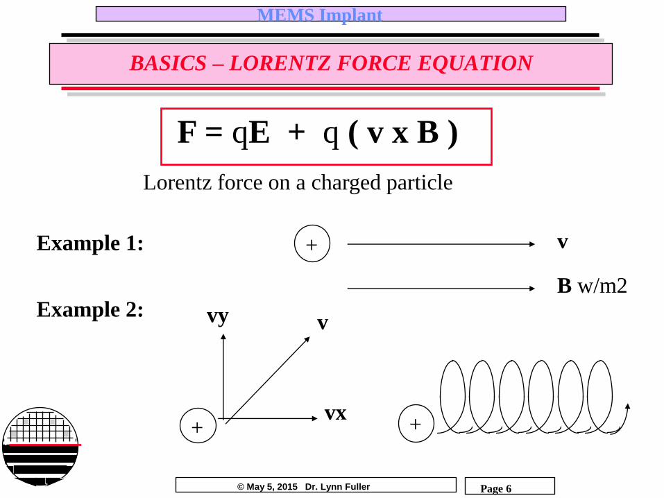
BASICS – LORENTZ FORCE EQUATION
+
vy
vx
v
v
B w/m2
+
+
Example 2:
Example 1:
F = qE + q ( v x B )
Lorentz force on a charged particle
© May 5, 2015 Dr. Lynn Fuller
MEMS Implant
Page 7
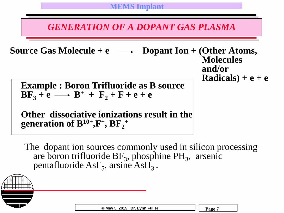
GENERATION OF A DOPANT GAS PLASMA
Source Gas Molecule + e Dopant Ion + (Other Atoms,
Molecules and/or Radicals) + e + e
Example : Boron Trifluoride as B source BF3 + e B+ + F2 + F + e + e
Other dissociative ionizations result in the generation of B10+,F+, BF2
+
The dopant ion sources commonly used in silicon processing
are boron trifluoride BF3, phosphine PH3, arsenic pentafluoride AsF5, arsine AsH3 .

© May 5, 2015 Dr. Lynn Fuller
MEMS Implant
Page 8
PLASMA SOURCE AND ION EXTRACTION
V extraction
( variable, typically ~30 KV )
Gas feed
To pump
Plasma Chamber
(positive) ions
mT level pressure
BF3
N
S
BF3
e B+ e
BF2+
M v 2 / 2 = q Vext
Solenoid
Arc
Voltage
19
5
27
2 1.6 10 30,0007.23 10
11 1.67 10
xmv x
sx
2 extqV
mn

© May 5, 2015 Dr. Lynn Fuller
MEMS Implant
Page 9
TYPICAL SOURCE SET UP
§ Pressure 30mT
§ Extraction Voltage 33 KV
§ Extraction Current 0.8 mA
§ Arc Voltage 2000 V
§ Arc Current 50 mA
§ Filament Current 150 A
§ Filament Voltage 20 V
§ Solenoid Current 3.0 A
Source Cabinet for Varian 120-10
© May 5, 2015 Dr. Lynn Fuller
MEMS Implant
Page 10
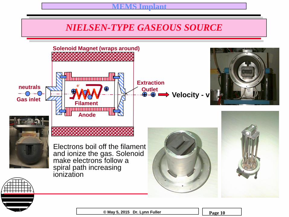
NIELSEN-TYPE GASEOUS SOURCE
Gas inlet
Anode
Filament
Extraction
Outlet
Solenoid Magnet (wraps around)
e-
+ + + +
neutrals
Velocity - v
Electrons boil off the filament and ionize the gas. Solenoid make electrons follow a spiral path increasing ionization

© May 5, 2015 Dr. Lynn Fuller
MEMS Implant
Page 11
SELECTION OF THE IONS TO BE IMPLANTED
The ions are extracted from the source and analyzed in a magnetic field. The Lorentz force makes the ions take a curved path with a radius of curvature that depends on the mass of each ionic species. By adjusting the magnetic field strength, only the selected ions will enter the accelerating column.
N
S
Ions Extracted
from Source Heavy Ions
Light
Ions
Selected Ions Analyzing
Magnet

© May 5, 2015 Dr. Lynn Fuller
MEMS Implant
Page 12
ION SELECTION - ANALYZING MAGNET
M /q = R2 B2 / (2 Vext)
Mass to charge ratio, M / q of the selected ions:
R
Resolving Aperture
R: radius of curvature
B
Magnetic
Field
v : ion velocity
Selected ions
Heavier ions
Lorentz = Centripetal Force force
q (n xB) = M n 2 / R
R=M n / q B
2 extqV
mn =
R is fixed, B and Vext are variable

© May 5, 2015 Dr. Lynn Fuller
MEMS Implant
Page 13
MAGNETIC SCAN COIL IN VARIAN 120-10
Analyzing Magnet
for mass
spectrometer
(Ion Selection)
Scan Magnet to give
X-scan

© May 5, 2015 Dr. Lynn Fuller
MEMS Implant
Page 14
PH3 GAS SPECTRUM
Beam
Current
(mA)
P31+
100
PH+
PH2+
1 2 3
PH3+
18 31 62 12
Ion Atomic Mass Units (AMU)
Phosphorus - 31
Hydrogen - 1

© May 5, 2015 Dr. Lynn Fuller
MEMS Implant
Page 15
BF3 GAS SPECTRUM
Ion Atomic Mass Units (AMU)
19 30 11 10 48 49
BF+ B11+
B10+
F+
B10(F)2+
Boron - 11
Fluorine - 19 BF2+
Beam
Current
(mA)
100

© May 5, 2015 Dr. Lynn Fuller
MEMS Implant
Page 16
ACCELERATING COLUMN
Resolving
Aperture Ground Vacc
E field
3 ‘ Column length =
Final Kinetic Energy of the Ion = q ( Vext + Vacc )
Example: Vext = 30 KV Vacc = 70 KV
Energy of the Ion= E= 100 KeV
level pressure

© May 5, 2015 Dr. Lynn Fuller
MEMS Implant
Page 17
ACCELERATION OF THE IONS
An acceleration voltage is applied across the column giving the ions their final kinetic energy. This voltage should be adjustable.
This shows 14 equal acceleration plates. If the desired acceleration
was 70KeV each section would contribute 5000 volts for example.

© May 5, 2015 Dr. Lynn Fuller
MEMS Implant
Page 18
VARIAN 400 ACCELERATION HARDWARE
Acceleration Column

© May 5, 2015 Dr. Lynn Fuller
MEMS Implant
Page 19
BF2 IMPLANTS
§ Boron mass = 11
§ Fluorine mass = 19
§ BF2 mass = 49
§ The energy divides by mass so 100 KeV BF2 is equivalent to 22.4 KeV B11 implant
§ BF2 peak is larger than B11 peak giving more current and shorter time for large dose implants
§ BF2 can give shallow implants
§ BF2 reduces channeling (explained in following pages)
© May 5, 2015 Dr. Lynn Fuller
MEMS Implant
Page 20
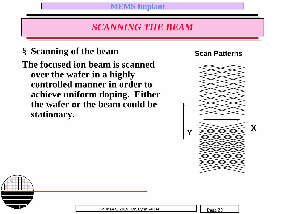
SCANNING THE BEAM
§ Scanning of the beam
The focused ion beam is scanned over the wafer in a highly controlled manner in order to achieve uniform doping. Either the wafer or the beam could be stationary.
Y X
Scan Patterns

© May 5, 2015 Dr. Lynn Fuller
MEMS Implant
Page 21
ELECTROSTATIC BEAM SCANNING
I) Electrostatic scanning (low/medium beam current implanters. I < 1mA)
This type of implanter is suitable for low dose implants. The beam current is adjusted to result in t=10 sec./wafer. With scan frequencies in the 100 Hz range, good implant uniformity is achieved with reasonable throughput.
Vy
Vx
Vertical Scan
Horizontal Scan
Si
wafer
© May 5, 2015 Dr. Lynn Fuller
MEMS Implant
Page 22
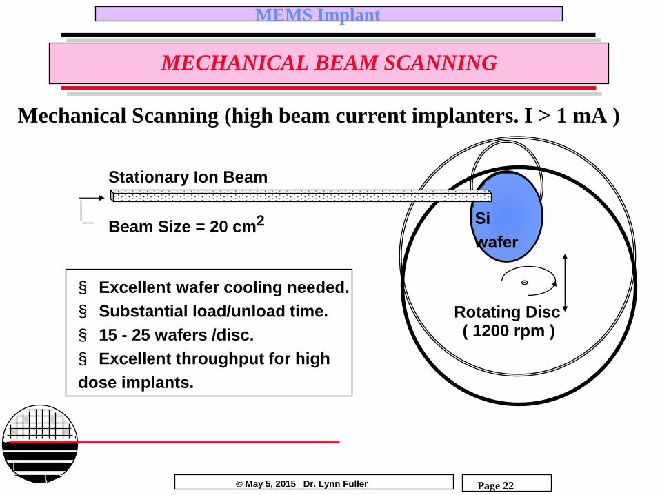
MECHANICAL BEAM SCANNING
Mechanical Scanning (high beam current implanters. I > 1 mA )
Stationary Ion Beam
Rotating Disc
Si
wafer Beam Size = 20 cm2
( 1200 rpm )
§ Excellent wafer cooling needed.
§ Substantial load/unload time.
§ 15 - 25 wafers /disc.
§ Excellent throughput for high
dose implants.

© May 5, 2015 Dr. Lynn Fuller
MEMS Implant
Page 23
MECHANICAL SCAN END STATION
© May 5, 2015 Dr. Lynn Fuller
MEMS Implant
Page 24
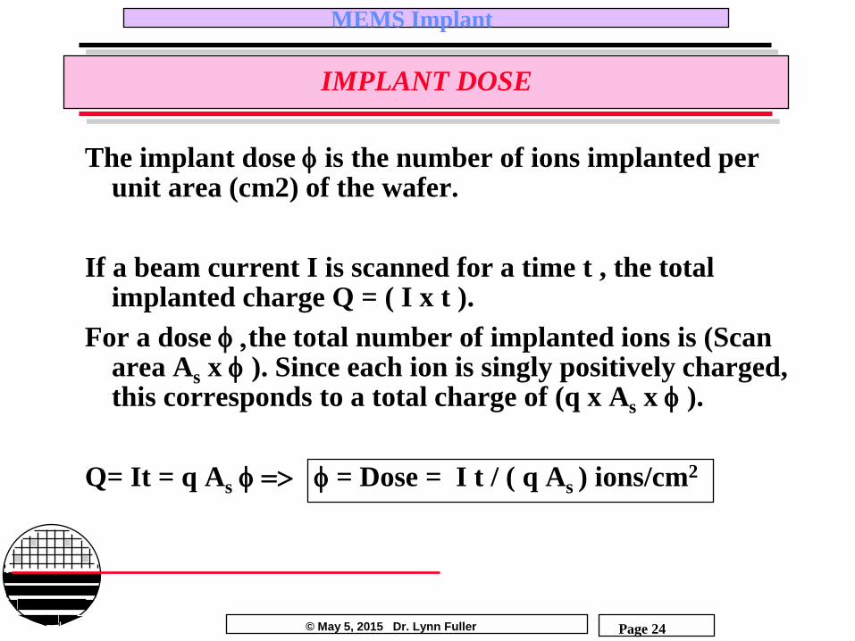
IMPLANT DOSE
The implant dose is the number of ions implanted per unit area (cm2) of the wafer.
If a beam current I is scanned for a time t , the total implanted charge Q = ( I x t ).
For a dose the total number of implanted ions is (Scan area As x ). Since each ion is singly positively charged, this corresponds to a total charge of (q x As x ).
Q= It = q As = Dose = I t / ( q As ) ions/cm2

© May 5, 2015 Dr. Lynn Fuller
MEMS Implant
Page 25
Beam Current
I in µA
Scanning Ion
Beam
Specimen
Current
Detector
Scan Position
XR
XL
XL XR
Faraday Cup
+
-
To Dose
Counter
and
Comparator
Current
Integrator
I
I
Detector/Wafer Holder
ION IMPLANT BEAM CURRENT SET UP
0
© May 5, 2015 Dr. Lynn Fuller
MEMS Implant
Page 26
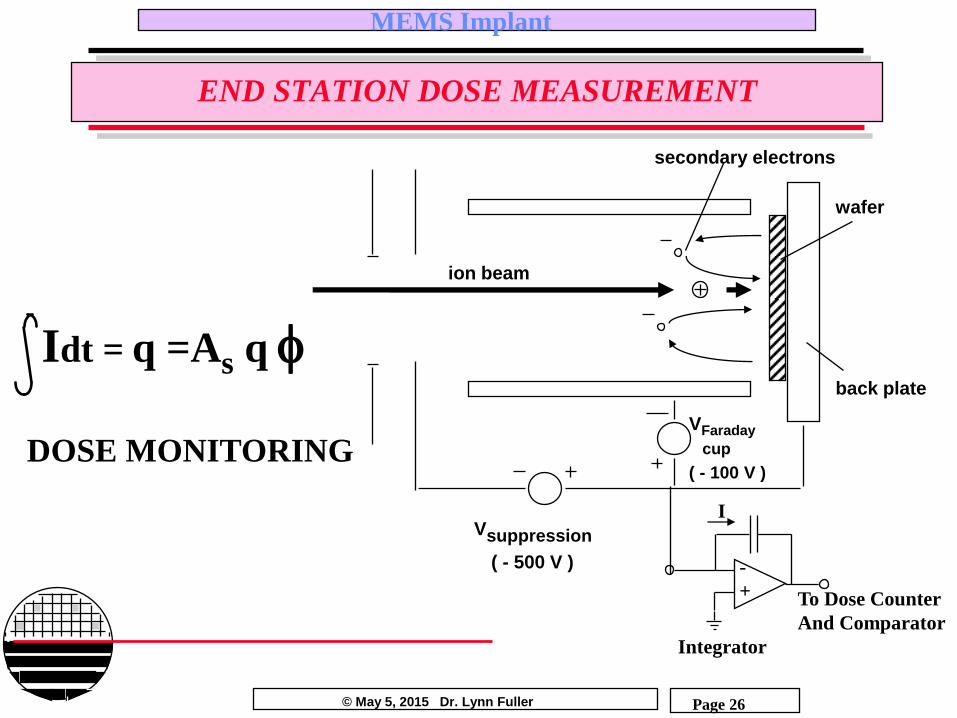
END STATION DOSE MEASUREMENT
Idt = q =As q
Vsuppression
( - 500 V )
VFaraday cup
( - 100 V )
ion beam
secondary electrons
wafer
back plate
DOSE MONITORING
-
+ To Dose Counter
And Comparator
Integrator
I

© May 5, 2015 Dr. Lynn Fuller
MEMS Implant
Page 27
COMPLETE SYSTEM

© May 5, 2015 Dr. Lynn Fuller
MEMS Implant
Page 28
DOPANT ION-SUBSTRATE INTERACTIONS
Upon entering the substrate, the ion slows down due to nuclear and electronic stopping.
Nuclear stopping :
Nuclear stopping is due to the energy transfer from the ion to Si nuclei. The interaction may be strong enough to displace the Si atom from its site ( only 15 eV needed to displace one Si atom ). The displaced Si atom may even have enough kinetic energy to displace several other Si atoms. Arsenic and Phosphorous ions lose their energy mostly by nuclear stopping. They cause substantial Si crystal damage when the implant dose exceeds 5E13/cm2.

© May 5, 2015 Dr. Lynn Fuller
MEMS Implant
Page 29
DOPANT ION-SUBSTRATE INTERACTIONS
Incident
ion
Silicon ( represents a Si atom )
Projected Range Rp
Ion at rest
Electronic stopping is due to the energy transfer from the ion to
the electrons of the host Si crystal. Boron ions lose their energy mostly by electronic stopping. Electronic stopping does not cause crystal damage.

© May 5, 2015 Dr. Lynn Fuller
MEMS Implant
Page 30
POST IMPLANT ANNEAL
The damaged crystal needs to be restored. This is typically achieved by 900 C, 30 min. furnace anneals or 1150 C, 30 sec. rapid thermal anneals.
The interstitial dopant ions become substitutional, thus donating carriers. The interstitial (displaced) silicon atoms become substitutional ,thus removing the defects that trap carriers and/or affect their mobility.
During the post implant anneal, dopant ions diffuse deeper into silicon. This must be minimized to maintain shallow junctions.

© May 5, 2015 Dr. Lynn Fuller
MEMS Implant
Page 31
ION IMPLANT EQUATIONS
after implant
Approximation
used in Vt
calculations
after anneal at
950 C, 15 min
-(X-Rp)2
2(Rp2+Dt) Approximation
N’ = Ni xi
After Anneal
N(x) = exp [ ]
N’
2 Rp2 + 2Dt
Gaussian Implant Profile
N(x) = exp [ ]
Rp = Range
Rp = Straggle From Curves }
-(X-Rp)2
2Rp2
N’
2 Rp
N’ = Dose = dt I
mqA
Ni
xi
where D is diffusion constant at the anneal temperature
t is time of anneal
x
con
centr
atio
n c
m-3
Rp
Cbackground
Npeak = Np

© May 5, 2015 Dr. Lynn Fuller
MEMS Implant
Page 32
ION IMPLANT RANGE
10 100
10-2
10-1
1
Implantation Energy (KeV)
Pro
jecte
d R
an
ge,
Rp
,(u
m)
B
P
As
Sb

© May 5, 2015 Dr. Lynn Fuller
MEMS Implant
Page 33
ION IMPLANT STANDARD DEVIATION
0.001
0.01
0.1
10 100 1,000 Implantation Energy (KeV)
Sta
nd
ard
De
via
tio
n,
R
p ,(u
m)
B
P
As
Sb

© May 5, 2015 Dr. Lynn Fuller
MEMS Implant
Page 34
CALCULATIONS
Using the equations on the previous pages: Find: Xj sheet Rho implant time surface conc. average doping
© May 5, 2015 Dr. Lynn Fuller
MEMS Implant
Page 35
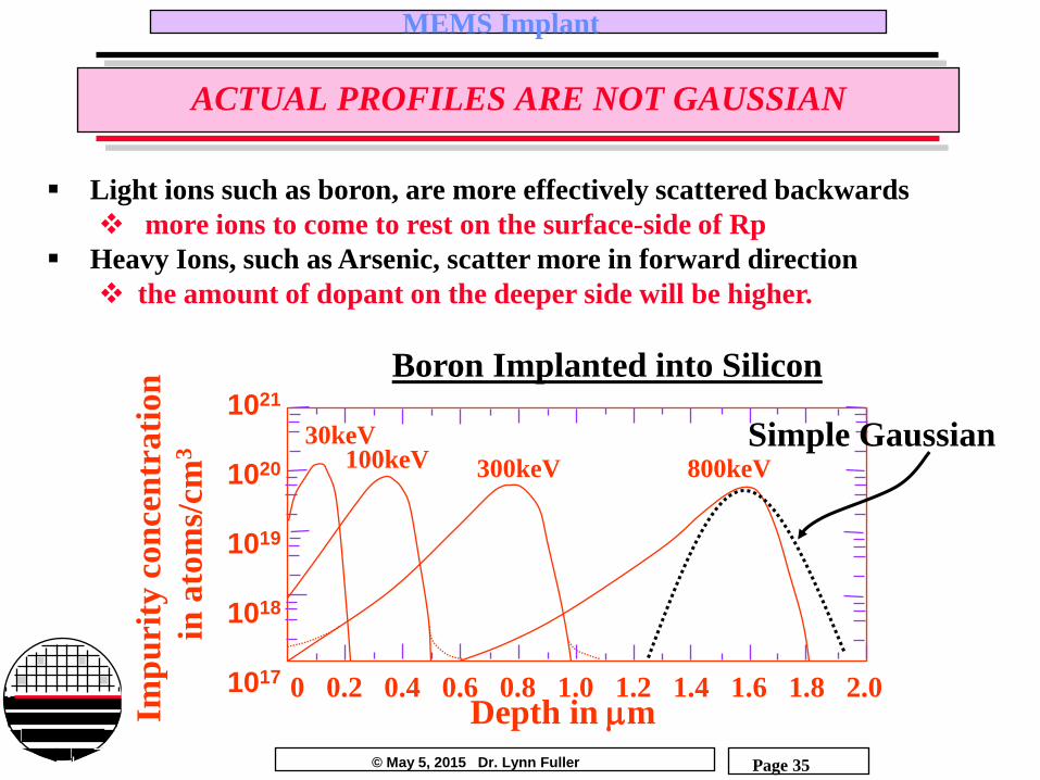
ACTUAL PROFILES ARE NOT GAUSSIAN
Light ions such as boron, are more effectively scattered backwards
more ions to come to rest on the surface-side of Rp
Heavy Ions, such as Arsenic, scatter more in forward direction
the amount of dopant on the deeper side will be higher.
Depth in m Imp
uri
ty c
on
cen
trati
on
in
ato
ms/
cm3
1021
1020
1019
1018
1017 0 0.2 0.4 0.6 0.8 1.0 1.2 1.4 1.6 1.8 2.0
Boron Implanted into Silicon
30keV 100keV 300keV 800keV
Simple Gaussian

© May 5, 2015 Dr. Lynn Fuller
MEMS Implant
Page 36
CHANNELING
§ Origin : the crystalline nature of the host substrate
Relative degree of openness of the silicon crystal for ions moving in <111>, <100> and <110> directions
: entrance angle
unchanneled ion: > cr
channeled
ion: < cr
Channeling process
(110) (100) (111)

© May 5, 2015 Dr. Lynn Fuller
MEMS Implant
Page 37
PREVENTING CHANNELING
Channeling does not occur if there is significant implant damage that turns the implanted layer into an amorphous one. Heavy ions like P31 and As75 at large doses do not show channeling.
Light ions and/or low dose implants are prone to channeling. In such instances, channeling can be prevented by:
1) Implanting through a thin amorphous layer (e.g. oxide).
2) Tilting and twisting the wafer to close crystal openness as seen by the ion beam.
3) Implanting heavy, but electrically inactive species like Si or Ar prior to the actual dopant implant. The pre-implant implant turns the wafer surface into an amorphous layer.

© May 5, 2015 Dr. Lynn Fuller
MEMS Implant
Page 38
SCREENING OXIDE
In addition to channeling prevention, implanting through a thin film layer (e.g. few 100 A of SiO2) offers the following advantages:
1) It prevents photoresist residues/deposits from reaching the silicon surface. The resist residues deposited on the thin film can subsequently be etched away with that film (e.g. SiO2 dipped in B.O.E.)
Silicon Wafer
oxide resist resist
resist deposit
2) It prevents excessive evaporation (out-gassing) of volatile species (e.g. As) during implant damage anneals.

© May 5, 2015 Dr. Lynn Fuller
MEMS Implant
Page 39
MASKING AGAINST ION IMPLANTS
Various thin films can be used to mask against ion implants : resist, oxide, nitride, polysilicon, etc. The most widely used combination is resist over the oxide. 1 to 1.5 µm thick resist blocks most of the ion implants encountered in silicon processing.Silicon dioxide slows down the ions at about the same rate as silicon does. Silicon nitride is a much stronger barrier to ions than silicon.
Dopant Density
Wafer Background
Doping
Implant
Doping
RESIST
O
X
I
D
E
SILICON

© May 5, 2015 Dr. Lynn Fuller
MEMS Implant
Page 40
MASKING WITH PHOTORESIST, POLY, AND OXIDE
N-type Substrate 10 ohm-cm
P-well N-well
6000 Å Field Oxide
B11, Dose = 2 E15, E = 50 KeV

© May 5, 2015 Dr. Lynn Fuller
MEMS Implant
Page 41
IMPLANT MASKING THICKNESS CALCULATOR
Rochester Institute of Technology Lance Barron
Microelectronic Engineering Dr. Lynn Fuller
11/20/04
IMPLANT MASK CALCULATOR Enter 1 - Yes 0 - No in white boxes
DOPANT SPECIES MASK TYPE ENERGY
B11 1 Resist 0 40 KeV
BF2 0 Poly 1
P31 0 Oxide 0
Nitride 0
Thickness to Mask >1E15/cm3 Surface Concentration 2961.954 Angstroms
© May 5, 2015 Dr. Lynn Fuller
MEMS Implant
Page 42
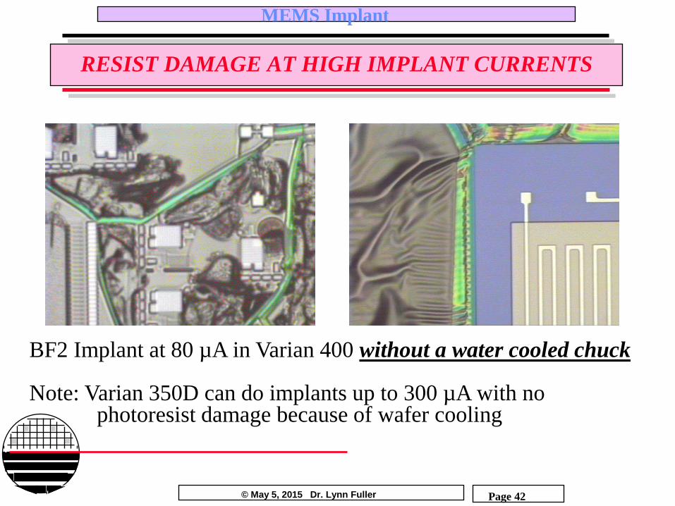
RESIST DAMAGE AT HIGH IMPLANT CURRENTS
BF2 Implant at 80 µA in Varian 400 without a water cooled chuck Note: Varian 350D can do implants up to 300 µA with no photoresist damage because of wafer cooling

© May 5, 2015 Dr. Lynn Fuller
MEMS Implant
Page 43
ION IMPLANT VS. CHEMICAL SOURCE PREDEPOSIT
Advantages of Ion Implant Low dose introduction of dopants is possible. In chemical source
predeposits dose values less than 5E13/cm2 are not achievable. Ion implant dose control is possible down to 1E11/cm2.
High dose introduction is not limited to solid solubility limit values. Dose control is very precise at all levels. Excellent doping uniformity is achieved across the wafer and from
wafer to wafer. Done in high vacuum, it is a very clean process step (except for out
gassing resist particulates due to excessive local power input). Drawbacks of Ion Implant
It requires very expensive equipment ( $1M or more). At high dose values, implant throughput is less than in the case of
chemical source predep.

© May 5, 2015 Dr. Lynn Fuller
MEMS Implant
Page 44
REFERENCES
1. Silicon Processing for the VLSI Era Volume I, S. Wolf and R.N.
Tauber, Lattic Press, Sunset Beach, CA, 1986.
2. The Science and Engineering of Microelectronic Fabrication,
S.A. Campbell, Oxford University Press, New York, NY, 1996.
3. VLSI Technology, Edited by S.M. Sze, McGraw-Hill Book
Company, 1983.
Top Related