


Languages
Pages
Legal


MANUAL MODIFICATION AND PLASMA EXPOSURE OF BORON NITRIDE
CERAMIC TO STUDY HALL EFFECT THRUSTER PLASMA CHANNEL
MATERIAL EROSION
By
ALEXANDER J. SATONIK
A THESIS
Presented to the Faculty of the Graduate School of the
MISSOURI UNIVERSITY OF SCIENCE AND TECHNOLOGY
In Partial Fulfillment of the Requirements for the Degree
MASTER OF SCIENCE IN AEROSPACE ENGINEERING
2013
Approved by
Dr. Joshua L. Rovey, Advisor
Dr. Serhat Hosder
Dr. Gregory Hilmas

© 2013
Alexander John Satonik
All Rights Reserved

iii
PUBLICATION THESIS OPTION
This thesis consists of the following articles that have been submitted for
publication as follows:
Pages 10-48 have been submitted and presented to the AIAA as paper AIAA-
2012-0198 at the 50th Aerospace Sciences Meeting in Nashville, TN. Jan. 9-12, 2012.
Pages 49-89 have been submitted to the AIAA Journal of Propulsion and Power.
Submitted 12/14/2012, in review.
iv
ABSTRACT
Worn Hall effect thrusters (HET) show a variety of unique microstructures and
elemental compositions in the boron nitride thruster channel walls. Worn thruster
channels are typically created by running test thrusters in vacuum chambers for hundreds
of hours. Studies were undertaken to manually modify samples of boron nitride without
the use of a hall effect thruster. Samples were manually abraded with an abrasive blaster
and sandpaper, in addition to a vacuum heater. Some of these samples were further
exposed to a xenon plasma in a magnetron sputter device.
Sandpaper and abrasive blaster tests were used to modify surface roughness
values of the samples from 10,000 Å to 150,000 Å, matching worn thruster values.
Vacuum heat treatments were performed on samples. These treatments showed the
ability to modify chemical compositions of boron nitride samples, but not in a manner
matching changes seen in worn thruster channels.
Plasma erosion rate was shown to depend on the grade of the BN ceramic and the
preparation of the surface prior to plasma exposure. Abraded samples were shown to
erode 43% more than their pristine counterparts. Unique surface features and elemental
compositions on the worn thruster channel samples were overwritten by new surface
features on the ceramic grains. The microscope images of the ceramic surface show that
the magnetron plasma source rounded the edges of the ceramic grains to closely match
the worn HET surface. This effect was not as pronounced in studies of ion beam
bombardment of the surface and appears to be a result of the quasi-neutral plasma
environment.
v
ACKNOWLEDGEMENTS
I would like to thank Dr. Rovey for his continued patience and support throughout
this project. I would also like to thank the rest of my committee members: Dr. Hosder
and Dr. Hilmas for their support and teaching. I also want to thank Mrs. Clarissa Wisner
for her excellent SEM images and St. Gobain Advanced Ceramics for their donation of
raw materials. A very special thanks to Dr. O’Keefe for his help in gaining access the
equipment at the MRC is also necessary.
I wish to recognize my lab co-workers for providing an exciting and educational
work environment and for their support in my experimental methods and classes. The
machinists Joe Boze, and Bob Hribar in the MAE Machine Shop for their tireless work
on the fabrication of an endless supply of pristine ceramic samples. I would like to thank
my parents, Susan and Robert Satonik, for their continued support and encouragement of
my academic pursuits. I also wish to thank all those that helped me edit and polish the
following pages.
On a lighter note I want to thank the MSM Spelunkers for always keeping my
weekends dirty. As is custom in the APLab I must thank Kapton™ tape for solving
every experimental setup problem. All problems can be solved with excessive
application of Kapton tape.
Lastly, I wish to thank all of my friends and those whom I did not mention by
name and remind them that you can never have too many pylons. Without their support I
could never have completed this project.

vi
TABLE OF CONTENTS
Page
PUBLICATION THESIS OPTION .............................................................................. iii
ABSTRACT ................................................................................................................. iv
ACKNOWLEDGMENTS ............................................................................................. v
LIST OF ILLUSTRATIONS ........................................................................................ ix
LIST OF TABLES ....................................................................................................... xi
SECTION
1. INTRODUCTION ......................................................................................... 1
1.1. PLASMA EROSION DESCRIPTIONS ........................................... 2
1.2. DESCRIPTION OF PAPERS .......................................................... 2
2. LITERATURE REVIEW ............................................................................... 4
2.1 THRUSTER TESTS ......................................................................... 4
2.2 CERAMIC SAMPLE TESTS ........................................................... 6
REFERENCES .................................................................................................. 8
PAPER
I. Modification of Boron Nitride Ceramic to Replicate Hall Effect Thruster
Surface Wear ................................................................................................... 9
ABSTRACT ................................................................................................... 9
NOMENCLATURE......................................................................................... 10
1. INTRODUCTION ....................................................................................... 10
2. SAMPLE CHARACTERIZATION METHODS .......................................... 13
2.1. SURFACE PROFILOMETRY ...................................................... 14
2.2. SCANNING ELECTRON MICROSCOPY ................................... 15

vii
2.3. ELECTRON DISPERSIVE X-RAY SPECTROSCOPY ................ 17
3. RESULTS ................................................................................................. 18
3.1. SANDPAPER MANUAL ABRASION ......................................... 18
3.1.1. Surface Roughness .......................................................... 19
3.1.2. SEM Images .................................................................... 20
3.1.3. EDS Analysis .................................................................. 22
3.2. ABRASIVE BLASTER ................................................................. 23
3.2.1. Surface Roughness .......................................................... 24
3.2.2. SEM Images .................................................................... 25
3.2.3. EDS Analysis .................................................................. 26
3.3. VACUUM HEATING ................................................................... 27
3.3.1. Surface Roughness .......................................................... 27
3.3.2. SEM Images .................................................................... 27
3.3.3. EDS Analysis .................................................................. 29
4. DISCUSSION .............................................................................................. 31
4.1. ROUGHNESS BY MANUAL ABRASION .................................. 31
4.1.1. Time or Distance Independent Roughness ....................... 32
4.1.2. Importance of Grit ........................................................... 33
4.1.3. Importance of Ceramic Grade .......................................... 35
4.2. SEM RESULTS DISCUSSION ..................................................... 35
4.3. EDS RESULTS DISCUSSION ...................................................... 39
4.3.1. Abrasion Sample EDS ..................................................... 39
4.3.2. Heated Sample EDS ........................................................ 40
5. CONCLUSION ............................................................................................ 41
REFERENCES ................................................................................................ 42
viii
II. Plasma Exposure of Hall Effect Thruster Ceramic Material ..................................... 45
ABSTRACT ................................................................................................. 45
NOMENCLATURE......................................................................................... 46
1. INTRODUCTION ....................................................................................... 46
2. EXPERIMENTAL SETUP AND CERAMIC SAMPLES ............................ 49
3. SAMPLE CHARACTERIZATION METHODS .......................................... 51
4. RESULTS ................................................................................................. 54
4.1. STEP HEIGHT .............................................................................. 54
4.2. ROUGHNESS ............................................................................... 57
4.3. ELEMENTAL COMPOSITION .................................................... 60
4.4. SEM IMAGES............................................................................... 65
5. DISCUSSION .............................................................................................. 71
5.1. MANUAL MODIFICATION LEADS TO INCREASED
EROSION ..................................................................................... 71
5.2. CHEMICAL COMPOSITION CHANGES .................................... 72
5.3 UNIFORMITY OF MICROSTRUCTURES ................................... 74
6. CONCLUSIONS .......................................................................................... 76
REFERENCES ................................................................................................ 79
SECTION
2. CONCLUSION ............................................................................................ 82
APPENDICES
A. RESULTS AND DISCUSSION OF PLASMA EXPOSED
GRADES A AND M ....................................................................... 84
B. BORON NITRIDE CERAMIC DATA SHEETS ............................. 91
VITA ................................................................................................. 95

ix
LIST OF ILLUSTRATIONS
Figure Page
1.1 Schematic of the basic operating principles of a Hall effect thruster (HET). ........... 1
PAPER I
1.1 Schematic of a Hall effect thruster. ...................................................................... 11
3.1 Surface roughness results for samples modified with 120 grit sandpaper. ............. 19
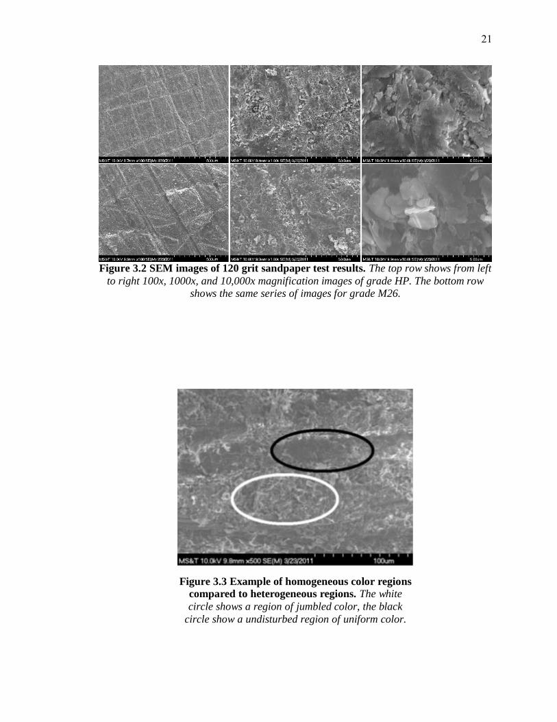
3.2 SEM images of 120 grit sandpaper test results. .................................................... 21
3.3 Example of homogeneous color regions compared to heterogeneous regions. ...... 21
3.4 Abrasive blaster roughness results for 220 grit abrasive particle size. ................... 24
3.5 SEM images of abrasive blaster test results. ......................................................... 25
3.6 Heated sample microstructure. ............................................................................. 29
4.1 Effect of grit number on maximum roughness results. .......................................... 32
4.2 Pits created by particle bombardment from 60 grit abrasive blaster. ..................... 35
4.3 Knobby microstructures. ...................................................................................... 37
4.4 Shielded sections of a worn HET. ........................................................................ 37
4.5 Comparison of all modification methods under SEM inspection. .......................... 38
x
PAPER II
2.1 The magnetron sputtering target. .......................................................................... 49
4.1 Step height of pristine and manually modified BN samples after plasma
exposure. ............................................................................................................. 55
4.2 Step height of worn thruster samples after plasma exposure. ................................ 56
4.3 Roughness of eroded and shielded sides of manually modified samples. .............. 58
4.4 Roughness of eroded and shielded sides of worn HET samples. ........................... 59
4.5 Grade HP and M26 manually modified pristine and plasma exposed
samples. ............................................................................................................... 67
4.6 Grade M26 thruster samples. ................................................................................ 69
4.7 Grade HP thruster samples. .................................................................................. 70
5.1 Locations of elemental spectrum analysis. ........................................................... 76
xi
LIST OF TABLES
Table Page
PAPER I
3.1 Sandpaper EDS results. ........................................................................................ 23
3.2 Abrasive blaster EDS results. ............................................................................... 26
3.3 Elemental compositions by weight of heated samples. ......................................... 30
4.1 Comparison of modification methods to properties changed. ................................ 31
PAPER II
2.1 Boron nitride sample matrix. ................................................................................ 50
2.2 Weight ratios of BN and binder chemicals in the different grades investigated. .... 51
4.1 Manually modified BN samples EDS and XPS results. ........................................ 61
4.2 Worn M26 thruster samples EDS data. ................................................................. 63
4.3 Worn HP thruster samples EDS data. ................................................................... 65
5.1 Elemental weight percentage of the spectrum sites. .............................................. 76
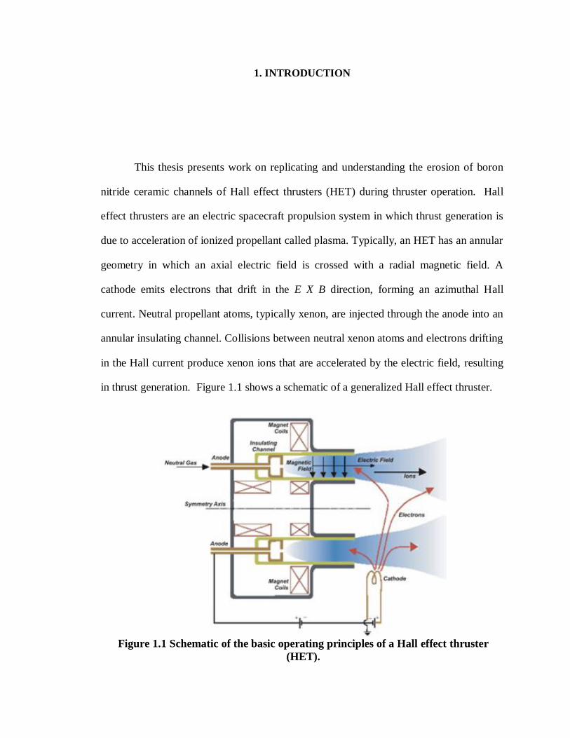
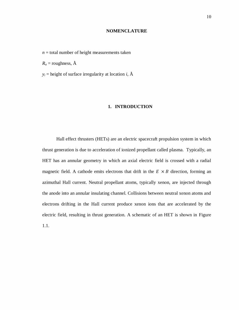
1. INTRODUCTION
This thesis presents work on replicating and understanding the erosion of boron
nitride ceramic channels of Hall effect thrusters (HET) during thruster operation. Hall
effect thrusters are an electric spacecraft propulsion system in which thrust generation is
due to acceleration of ionized propellant called plasma. Typically, an HET has an annular
geometry in which an axial electric field is crossed with a radial magnetic field. A
cathode emits electrons that drift in the E X B direction, forming an azimuthal Hall
current. Neutral propellant atoms, typically xenon, are injected through the anode into an
annular insulating channel. Collisions between neutral xenon atoms and electrons drifting
in the Hall current produce xenon ions that are accelerated by the electric field, resulting
in thrust generation. Figure 1.1 shows a schematic of a generalized Hall effect thruster.
Figure 1.1 Schematic of the basic operating principles of a Hall effect thruster
(HET).
2
1.1. PLASMA EROSION DESCRIPTIONS
The plasma used as propellant in the HET is produced within and expelled from a
ceramic channel, typically composed of boron nitride. During operation the plasma
erodes the ceramic channels eventually wearing the channels to the point that the
magnetic coils become exposed to the plasma, which are then eroded as well, resulting in
an end-of-life condition for the thruster. In addition the surface properties of the HET
discharge channel change due to thruster operation. At the macroscopic level, surface
roughness increases, especially near the exit plane where angled striations in the channel
are formed. At the microscopic level, metallic atoms are deposited on the BN channel
close to the anode and individual BN grains have their edges rounded [1].
The surface properties of the ceramic can also affect thruster performance.
Properties of the HET channel wall affect secondary electron emission (SEE), anomalous
electron transport near-wall conductivity and erosion rate, thereby altering HET
performance [2,3]. The roughness of HET channel walls has been shown to effect the
equipotential contours of the plasma sheath near the channel wall reducing overall
thruster performance [4]. Raitses, et al., show that wall materials having higher SEE
reduce the electron temperature within the HET discharge channel, thereby reducing
thruster performance [5,6].
1.2. DESCRIPTION OF PAPERS
In this thesis two papers are presented which describe attempts to reproduce
characteristics of worn HET ceramic channels on samples of boron nitride. Paper I
focuses on the manual modification of pristine samples of grades HP, A, M, and M26 of
boron nitride through abrasive techniques and heat treatment. Samples from worn HETs
3
are also modified. Paper II explores how boron nitride samples erode when under plasma
exposure. Pristine, manually modified, and worn HET channel samples were exposed to
a plasma source and the surface properties before and after exposure were studied. These
papers are preceded by an introduction and literature review which gives some brief
details on the importance of surface characteristics to HET operation, and details of what
surface features are created during the operation of HETs.

4
2. LITERATURE REVIEW
Studies into the material properties and erosion characteristics of Hall effect
thruster channel materials have been ongoing since the first flights of electric propulsion
devices in the 1960’s. The majority of these experiments were concerned with the
erosion rates of the wall materials to determine the operational lifetime of the thruster.
These tests typically involved a test thruster operating in a vacuum facility for extended
periods of time to create the worn material samples. Other materials experiments used ion
beam sources to eroded samples of channel wall materials.
Many other areas of research are focused on using modeling and simulation to
predict the erosion rates of thruster walls. These models are often compared with the
previously mentioned experiments as a means to validate the models predictions. Most
of these models only look at the erosion rate and do not include simulations of changing
material compositions or unique microstructures that have been observed in worn thruster
samples. As such discussion of models and simulations of erosion is limited in this
paper.
2.1. THRUSTER TESTS
A wide variety of thrusters are tested in laboratory conditions to validate the
thruster design for flights or to generate test data and samples. These tests typically run
the thruster for several hundred to a few thousand hours. At least one test ran a thruster
for over 10,000 hours [7].

5
These tests often have common characteristics when looking at the erosion of the
ceramic channels during operation [8]. Thruster channel erosion rates tend to slow as
thruster operation time increases. This phenomenon was strongly present in the 10,000
hour test where nearly all of the erosion took place in the first half of the test with the
erosion rate in the later half being nearly indistinguishable from the noise in the
measurement equipment. Thrusters do not wear in a uniform fashion The erosion will
chamfer the corners of the channel at the exit plane and continue to increase the radius of
curvature of the chamfer. The inner wall of the channel will have more erosion than the
outer wall in the same thruster. Thrusters of smaller diameter have been noted to have
shorter lifetimes due to the erosion rate having poor correlation to overall thruster size
[8]. Unfortunately for this study most thruster tests focus on the performance aspect of
the design, particularly thruster output and drift current. They offer only minimal
analysis on the erosion characteristics beyond what is necessary to predict an operational
lifetime for the particular model.
In an effort to better understand the details of the erosion of boron nitride
ceramics, studies of worn thruster channels were conducted by Zidar [1]. These studies
showed significant variations in microstructures and chemical compositions throughout
the thruster channel. Samples near the anode in the bottom of the channel showed the
least erosion but had the most contaminant elements. Near the exit plane the amount of
erosion increased as expected and the amount of contaminant elements decreased, likely
from sputter cleaning. Also, microstructures showed more rounding closer to the exit
plane. The ratio of boron nitride to binding agent also changed with respect to azimuthal
location. The binding agent with respect to BN ceramic grades is a component of the
ceramic that is not boron nitride, but is used to hold the grains of boron nitride together.
The ratio of boron nitride to binding agent increased with proximity to the exit plane.

6
2.2. CERAMIC SAMPLE TESTS
There is a considerable body of work surrounding the study of the boron nitride
ceramics used in thruster channels. A popular technique to study sputter erosion is to
bombard ceramic samples with an ion source and collect the ejected debris with a quartz
crystal microbalance. This method allows for both an estimate of erosion rate based on
the total amount of material collected and an analysis of the element species sputtered
through spectrometry tests of the collected debris on the microbalance. Direct weight
loss measurements of boron nitride ceramic samples have poor repeatability due to the
hydroscopic nature of the material and due to the impingement of ions within the crystal
structure.
Experiments done by Yalin using the quartz crystal microbalance (QCM) method
showed an abundance of monoatomic boron in the sputter debris. Yalin’s experimental
setup also allowed for the sample to be bombarded at an angle with respect to the ion
beam. A strong asymmetry was noted in the erosion pattern when the sample was at an
angle [9]. Similar experiments by Garnier had some differing results. Garnier noted an
abundance of molecular sized sputter debris but he did find that the surface chemistry had
an increase in the binding agent signature and a decrease in the boron and nitrogen
signatures [10]. Garnier further found that angle had only a small effect on sputter rate
due to the surface roughness of the samples being several orders of magnitude greater
than the scale of the sputter erosion. An explanation in the differences in the sputter
debris may lie in the different grades of boron nitride used in the experiments. Yalin
used a grade HP boron nitride which is primarily composed of boron nitride with roughly
6% binding agent of calcium borate. Garnier used a boron nitride ceramic with silicon
dioxide binding agent in a 4:1 ratio of boron nitride to silicon dioxide as measured prior
to sputter erosion.
7
Experiments done with various grades of boron nitride ceramic also indicate that
various grades of boron nitride ceramic erode at different rates. An experiment by
Peterson used a single HET with five ceramic channels each made of a different grade of
boron nitride ceramic [11]. Based on composite material sputter theory the binding agent
should erode before the boron nitride since it has weaker chemical bonds. However the
most pure grades of BN ceramic were not the most resilient to erosion. Peterson found
that grade HP had the least erosion and grade M had the most erosion. Grade HP is
composed of 94% BN, grade A is composed of 98% BN, grade M26 has 60% BN and
grade M has just 40% BN by weight. In contrast to the unexpected erosion rates of the
best performing ceramics, grade M had the highest ratio of binding agent to boron nitride.
Peterson did not consider how the differences in mechanical and thermal properties could
have influenced the erosion rates.
8
REFERENCES
[1] Zidar, D. G., Rovey, J. L., “Hall-effect Thruster Channel Surface Properties
Investigation,” Journal of Propulsion and Power, vol. 28 No. 2 , 2012, pp. 334-
343.
[2] Morozov, I A., “The Conceptual Development of Stationary Plasma Thrusters,”
Plasma Physics Reports, Vol. 29, No. 3, 2003, pp. 235-250. (Translated from
Russian. Originally published in Fizika Plazmy, Vol 29, No, 3,pp. 261-276.)
[3] Raitses, Y., Staack, D., Keidar, M. and Fisch, N. J., “Electron-wall interaction in
Hall thrusters,” Physics of Plasmas, Vol. 12. No. 5, 2005, pp. 057104-1 – 057104-
9.
[4] Zhurin, V. V., Kaufman, H. R. and Robinson, R. S., “Physics of closed drift
thrusters,” Plasma Sources Science and Technology, Vol. 8, No. 1, 1999, pp. R1-
R20.
[5] Raitses, Y., Smirnov, A., Staack, D. and Fisch, N. J., “Measurements of
secondary electron emission effects in the Hall thruster discharge,” Physics of
Plasmas, Vol. 13, No. 1, 2006, pp. 014502-014502-4.
[6] Choueiri, E. Y., “Fundamental Difference Between the Two Hall Thruster
Variants,” Physics of Plasmas, Vol. 8, No. l, 2001, pp. 5025-5033.
[7] de Grys, K., Mathers, A., Welander, B. and Khayms, V., “Demonstration of
10,400 Hours of Operation on a 4.5 kW Qualification Model Hall Thruster,” 46th
AIAA/ASME/SAE/ASEE Joint Propulsion Conference &Exhibit, AIAA, 2010.
[8] Mason, L. S., Jankovsky, R. S. and Manzella, D. H.,”1000 Hours of Testing on a
10 Kilowatt Hall Effect Thruster,” 37th AIAA /ASME/SAE/ASEE Joint Propulsion
Conference and Exhibit, AIAA, 2001.
[9] Yalin, A.P., Rubin, B., Domingue, S.R., Glueckert, Z., and Williams, J.D.,
“Differential Sputter Yields of Boron Nitride, Quartz, and Kapton Due to Low
Energy Xe+ Bombardment,” 43rd AIAA/ASME/SAE/ASEE Joint Propulsion
Conference, AIAA paper 2007: 5314.
[10] Garnier, Y., Viel, V., Roussel, J. F., Pagnon, D., Mange, L. and Touzeau, M.,
“Investigation of Xenon Ion Sputtering of One Ceramic Material Used in SPT
Discharge Chamber,” 26th International Electric Propulsion Conference, IEPC,
1999, pp. 512-517.
[11] Peterson, P. Y., Jacobson, D. T., Manzella, D. H. and John, J. W., “The
Performance and Wear Characterization of a High-Power High-Isp NASA Hall
Thruster,” 41st AIAA /ASME/SAE/ASEE Joint Propulsion Conference and Exhibit,
AIAA, 2005.

9
PAPER
I. Modification of Boron Nitride Ceramic to Replicate Hall
Effect Thruster Surface Wear
Alexander J. Satonik and Joshua L. Rovey
Missouri University of Science and Technology, Rolla, MO, 65409
ABSTRACT
Pristine and worn Hall effect thruster boron nitride channel materials show
significant differences in surface features, and chemical compositions. Worn thruster
channels are typically created by running test thrusters in vacuum chambers for hundreds
of hours. This paper studies ways to manually modified pristine samples of boron nitride
without the use of a Hall-effect thruster. Sandpaper and abrasive blaster tests were used
to modify surface roughness values of sample from 10,000 Å to 150,000 Å. These values
match the range of surface roughness seen in worn Hall effect thrusters. Vacuum heat
treatments were performed on samples, these treatments showed the ability to modify
chemical compositions of boron nitride samples but not in a manner matching changes
seen in worn thruster channels.
10
NOMENCLATURE
n = total number of height measurements taken
Ra = roughness, Å
yi = height of surface irregularity at location i, Å
1. INTRODUCTION
Hall effect thrusters (HETs) are an electric spacecraft propulsion system in which
thrust generation is due to acceleration of ionized propellant called plasma. Typically, an
HET has an annular geometry in which an axial electric field is crossed with a radial
magnetic field. A cathode emits electrons that drift in the direction, forming an
azimuthal Hall current. Neutral propellant atoms, typically xenon, are injected through
the anode into an annular insulating channel. Collisions between neutral xenon atoms and
electrons drifting in the Hall current produce xenon ions that are accelerated by the
electric field, resulting in thrust generation. A schematic of an HET is shown in Figure
1.1.

11
Many current HET efforts are focused on developing and benchmarking models
that integrate the important role of surface properties of the annular channel that contains
the plasma discharge [1-9]. Wall-effects play an important role in both the lifetime and
overall performance of the thruster. Properties of the channel wall can affect secondary
electron emission (SEE), anomalous electron transport, and nearwall conductivity,
thereby altering HET performance [10-13]. Further, wall properties are an important
factor in the sputter erosion processes that are known to limit thruster lifetime [14-17].
Current HET models do not integrate a realistic wall microstructure, but instead rely on
sputter yield or SEE coefficients derived from idealized material tests [5,9,18]. The
results presented below show that through various methods of modification some of the
surface properties observed in worn HET discharge channels can be reproduced.
Properties of the HET channel wall affect SEE, anomalous electron transport, and
near-wall conductivity, and erosion rate, thereby altering HET performance [10,11]. The
Figure 1.1 Schematic of a Hall effect thruster.

12
roughness of HET channel walls has been shown to affect the equipotential contours of
the plasma sheath near the channel wall reducing overall thruster performance [19].
Raitses, et al., show that wall materials having higher SEE reduce the electron
temperature within the HET discharge channel, thereby reducing thruster performance
[13,20]. Determining the influence of material surface properties on SEE in HETs is
difficult due to the complexity of electron-wall interaction, which must include factors
such as roughness, composition, non-Maxwellian electron distribution, and multiple
electron scattering processes all of which influence SEE yield, and as such have some
level of influence on HET performance [6]. The sputter yield (atoms removed per
incident ion) of the ceramic surface of a typical HET channel wall has been found to be
dependent upon the roughness of the ceramic surface [24,25].
The surface properties of the HET discharge channel change due to thruster
operation. Previous results have shown that the BN channel surface changes considerably
after a few 100 hours of operation. Zidar and Rovey compared pristine and worn grade
HP and M26 boron nitride channel material from various locations within thrusters and
showed that surface changes occur on multiple length scales and vary depending on the
location [1-3]. At the macroscopic level, surface roughness increases, especially near the
exit plane where angled striations in the channel are formed. Near the anode deposition of
metallic materials was evident. At the microscopic level, metallic atoms are deposited on
the BN channel close to the anode and individual BN grains become smoother. Both
Garnier, et al., [23-24] and Zidar, et al., [1-3] show that the chemical composition of the
BN channel surface changes, with the fraction of silicon dioxide binding agent decreasing
with proximity to the exit plane of the thruster. It is currently unclear how these surface
changes affect SEE and sputter yield, and indirectly affect performance and lifetime.
13
The goal of this study is to develop methods for replicating the worn surface
features of the BN channel without operating it for extended duration inside an HET.
Future studies can then analyze the effects of changes in surface features on SEE and
sputter yield without expensive long duration modification of samples by HET operation.
In the following sections three manual modification methods to replicate the surface
characteristics of a worn HET BN channel are presented. Sandpaper and abrasive blaster
modification methods were used for changing the surface roughness. Vacuum heating
was used to attempt to modify the sample microstructure and chemical composition.
Manually modified sample surfaces were characterized using surface profilometry,
scanning electron microscopy, and energy dispersive spectroscopy. Manually modified
surface characteristics are compared with those of worn HET samples to determine the
modification methods that best replicate the worn HET channel surface.
2. SAMPLE CHARACTERIZATION METHODS
Three surface characterization methods were used on the manually modified BN
samples. Each sample was characterized using surface profilometry, scanning electron
microscopy (SEM), and energy dispersive x-ray spectroscopy (EDS). Profilometry
quantifies the surface roughness of the sample, while SEM provides a qualitative
comparison of the microscopic topography of the samples. EDS is used to quantify the
atomic constituents on the surface of each sample.
14
Samples were cut from large blocks of ceramic material. The grade HP boron
nitride was cut on a lathe using a carbide bit since the large block of material came in the
form of a large rod. The grade M26 material came in thick sheets and had square
samples milled out of it on a 3-axis mill using a small carbide bit. The faces of both
samples were finished using the same tool and bit that was used to cut them from the
original block of ceramic material.
2.1. SURFACE PROFILOMETRY
Surface profilometry determines surface roughness by measuring the height of
finely spaced irregularities. Quantitatively, surface roughness is measured as the height of
surface irregularities with respect to an average line. Roughness is expressed in units of
length; in the case of this study, roughness is expressed in angstroms. In this
investigation, roughness, termed Ra, is determined using the arithmetical average, as
defined in Eqn. 1:
∑
For this investigation, surface profilometry is performed using a Sloan Dektak IIA
surface measuring system. The Dektak IIA is capable of measuring surface features
having heights ranging from less than 100 Å to 655,000 Å [28]. Calibration and
verification of accurate roughness measurements are conducted both before and after the
(1)
15
roughness studies performed using this instrument. In all cases the profilometer is found
to be accurate within the specified ±5% for all standards measured, which covered the
specified measurement range from 100 Å to 655,000 Å [28]. Scanning electron
microscope images of the tracks made by the scanning stylus of the profilometer
demonstrate that the profilometer stylus tip has a characteristic width of 10-15 μm. The
geometry of the stylus tip is assumed to be approximately hemispherical. The
characteristic width of the stylus tip constrains the size of the surface features which can
be measured in the direction of travel of the stylus tip. Therefore the profilometer can
make vertical measurements of surface having characteristic heights in the range of
100’s of Å, while the measurements of the horizontal lengths of these features are
limited to the 10’s of μm. This model profilometer is a single line profilometer,
meaning the roughness can only be measured along a single line on the sample surface.
To better ensure that the roughness measurements reflect the roughness of an entire
sample surface, multiple scans were taken at multiple locations.
2.2. SCANNING ELECTRON MICROSCOPY
A scanning electron microscope (SEM) uses electrons to produce images of
surface features as low as 10 nm in size. An SEM operates by using an electron column
consisting of an electron gun and two or more electrostatic lenses in a vacuum. The
electron gun provides a beam of electrons having energies in the range of 1-40 keV, and
the beam is reduced in diameter by electrostatic lenses to generate sharper images at high
magnification. The electron beam interacts with the sample and penetrates roughly a
micrometer into the surface, where electrons from the beam are backscattered and

16
secondary electrons are emitted. Detectors collect the backscattered and secondary
electrons, and these electron signals are used to generate the magnified image of the
specimen [31].
Secondary electrons emitted by the sample material are necessary to image the
sample. Non-conducting insulators generally have poor secondary electron emission
characteristics, in which case a conductive coating is often applied to provide high
resolution, high magnification images. The ceramic specimens considered in this study
are insulators, and a conductive coating is applied to provide the best imaging possible. In
this study, a thin layer of 60:40 gold-palladium alloy is applied to the samples. The
samples are placed into a vacuum chamber where the gold-palladium is sputtered onto
the sample surface in a thin coat approximately 10 nm thick. The gold-palladium alloy
provides high secondary electron emission, while still providing a thin, continuous film
with minimal agglomeration regions. This thin coating provides the necessary secondary
electrons for high resolution images, without obscuring the images of the underlying
microstructure.
A Hitachi S-4700 scanning electron microscope was used to image the surface of
each sample. It is capable of producing images with magnification greater than 500,000
times, and can resolve structures up to 2 nm across. For this investigation, micrographs
were taken of each sample at magnifications of 30, 100, 400, 1,000, 5,000, and 10,000
times.
17
2.3. ENERGY DISPERSIVE X-RAY SPECTROSCOPY
The SEM used in this investigation has energy dispersive x-ray spectroscopy
(EDS) capability. EDS is a variant of x-ray fluorescence spectroscopy, and is used for
chemical characterization and elemental analysis. EDS is performed by a SEM which has
been installed with the necessary detection equipment. The electron column creates an
electron beam focused on the sample surface. This focused electron beam results in the
generation of an x-ray signal from the sample surface. The x-rays generated from the
interaction of the focused electron beam and the sample surface pass through a beryllium
window separating the specimen vacuum chamber and the Lithium-drifted Silicon
detector. Within the detector, the photons pass into a cooled, reverse-bias p-i-n (p-type,
intrinsic, n type) Si(Li) crystal. The Si(Li) crystal absorbs each x-ray, and in response
ejects a photoelectron. The photoelectron gives up most of its energy to produce electron-
hole pairs, which are swept away by the bias applied to the crystal, to form a charge
pulse. The charge pulse is then converted into a voltage pulse, which is then amplified
and shaped by a series of amplifiers, converters, and an analog-to-digital converter where
the final digital signal is fed into a computer X-ray analyzer (CXA) [31]. A histogram of
the emission spectrum from the sample is obtained and analyzed by the CXA to
determine the percent by weight of elements present in the sample. For this study, EDS
analysis was conducted using an EDAX energy dispersive x-ray unit attached to the
Hitachi S4700 SEM. Data provided by EDS was the chemical composition of the sample
regions by both percent of atoms and percent by weight.
18
3. RESULTS
Samples of BN were manually modified. Two grades of BN were used. Grade HP
is made of boron nitride and a calcium borate - boric acid binder mixture with a trace
amount of silicon dioxide. Grade M26 is composed of a 60-40 mix by weight of boron
nitride and silicon dioxide. These BN grades were modified using sandpaper manual
abrasion, abrasive blasting, and vacuum heating. Results from surface characterization of
manually modified samples are presented below. Surface roughness, surface images, and
surface atomic composition results are presented from the surface profilometry, SEM,
and EDS analysis of sandpaper, abrasive blasting, and vacuum heating modified samples.
3.1. SANDPAPER MANUAL ABRASION
Two samples of HP grade and two samples of M26 grade BN were modified with
120 grit sandpaper. Only one sample of each grade was modified with 60, 220, and 400
grit sandpaper. The sandpaper used in this experiment used aluminum dioxide as its
abrasive component, the sandpaper used was also commercially available and obtained
from the local home improvement store. A sample of BN was secured to the bottom of a
plastic pull tab, on top of which a 200 gram weight was placed to maintain a constant
frictional force between the sample and sandpaper. The weight on the sample was held
constant between different tests, and the distance the sample was dragged is done in
measured increments. In between distance increments the orientation of the sample is
rotated by 90 degrees in an attempt to give a more even wear pattern.
19
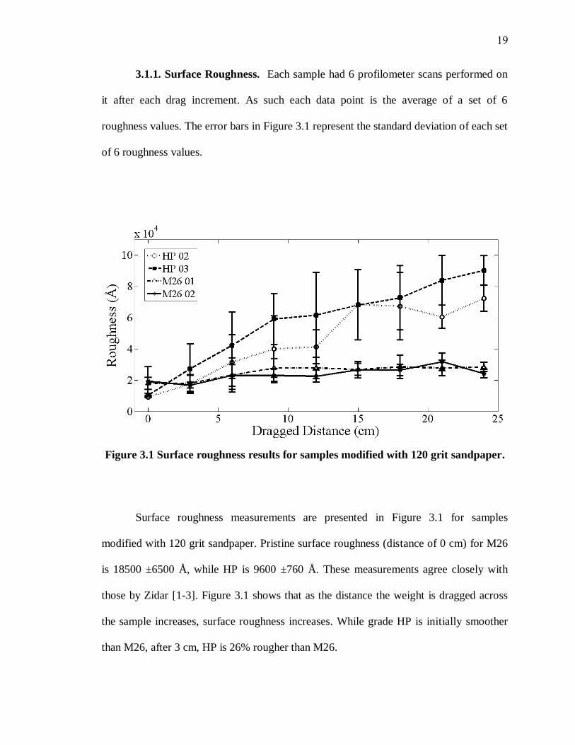
3.1.1. Surface Roughness. Each sample had 6 profilometer scans performed on
it after each drag increment. As such each data point is the average of a set of 6
roughness values. The error bars in Figure 3.1 represent the standard deviation of each set
of 6 roughness values.
Surface roughness measurements are presented in Figure 3.1 for samples
modified with 120 grit sandpaper. Pristine surface roughness (distance of 0 cm) for M26
is 18500 ±6500 Å, while HP is 9600 ±760 Å. These measurements agree closely with
those by Zidar [1-3]. Figure 3.1 shows that as the distance the weight is dragged across
the sample increases, surface roughness increases. While grade HP is initially smoother
than M26, after 3 cm, HP is 26% rougher than M26.
Figure 3.1 Surface roughness results for samples modified with 120 grit sandpaper.
20
The grade M26 samples had a final roughness value 60% and 25% greater than
the roughness value measured prior to abrasion, respectively; while the HP samples had a
roughness increase of 8 and 8.75 times respectively, after the full 24 cm drag distance.
3.1.2. SEM Images. Images of a sandpaper modified sample were taken after the
final interval of abrasion was performed, that is after a drag distance of 24 cm. Due to the
requirement of a conductive coating that has to be applied to the sample for imaging,
samples are only imaged once they are finished with the specific experiment, to ensure
that the coating agent does not affect the roughness measurements.
Figure 3.2 on the following page shows the SEM images of the sandpaper
modified samples. At lower magnifications the groves from the sandpaper can be clearly
seen. At higher magnifications (1000x) the grooves display an appearance more
heterogeneous in color compared to the darker more uniform regions adjacent to them.
The highest magnification images show plates made of many individual particles,
arranged in a random orientation as a result of being disturbed by the abrasion process.
Upon closer inspection in Figure 3.3 the 10,000x magnification images the
individual grains in the darker regions appear to have a more uniform orientation and
undisturbed structure. This suggests that the more heterogeneous color regions are the
regions that experienced damage from the sandpaper abrasion process.
21
Figure 3.3 Example of homogeneous color regions
compared to heterogeneous regions. The white
circle shows a region of jumbled color, the black
circle show a undisturbed region of uniform color.
Figure 3.2 SEM images of 120 grit sandpaper test results. The top row shows from left
to right 100x, 1000x, and 10,000x magnification images of grade HP. The bottom row
shows the same series of images for grade M26.

22
3.1.3. EDS Analysis. Analysis of the elemental composition of BN samples after
modification with sandpaper show an increase in trace elements and oxygen content. Due
to the imaging agent required to coat the sample for use in the SEM, all of the samples
were unique and had only one test performed on them. For example the sample used for
the pristine chemical analysis of grade HP was a different sample then the sandpaper
abraded grade HP sample. Pristine grade HP is composed of 4.5% trace elements. Trace
elements being those elements that are not boron, nitrogen, or oxygen. After modification
the trace elements make up 10.9% of the weight of the grade HP sample. The pristine
element composition of grade M26 is made up of 3.4% trace elements. After
modification the trace elements account for 3.5% of the weight. Trace elements in grade
M26 are those elements not boron, nitrogen, silicon, or oxygen. Of the non-trace
elements oxygen has a 11.5% increase by weight in the grade HP sample, and a 12.5%
increase by weight in the grade M26. Boron and nitrogen have a loss in weight of 5.5%
and 11.4% in grade HP respectively, and 11.3% and 14.6%, respectively, in grade M26.
Silicon has a 2% increase in grade M26. In grade HP silicon is considered a trace element
and not used as a primary binding agent. The full results are shown in Table 3.1.
23
Table 3.1 Sandpaper EDS results.
Grade HP Weight% Grade M26 Weight%
Element Pristine Sandpaper Element Pristine Sandpaper
B 27.73 22.06 B 23.2 20.57
N 59.55 48.17 N 29.54 25.22
O 7.28 18.84 O 24.42 30.68
Si 0.19 0.5 Si 19.45 20.02
C 2.92 5.26 C 3.28 3.28
Ca 0.48 2.94 Na 0 0.12
Na 0 0 Al 0.12 0.11
F 0.95 1.83 K 0 0
Al 0 0.08 Ca 0 0
Cl 0 0.14 Cl 0 0
K 0 0.18 S 0 0
3.2. ABRASIVE BLASTER
A sample of each grade of BN was modified with an abrasive blaster. A small
tower was constructed to hold the model 260 Badger mini sandblaster at a constant height
above the BN samples. The tower allows for an adjustable height to ensure that the cone
of grit exiting the nozzle of the blaster can completely cover the sample. A height of 18
cm gave good sample coverage without eroding the sample too quickly. The samples of
BN are exposed to the abrasive grit in short increments of 2 seconds. The compressed air
was supplied at 23 psi. The blaster uses aluminum dioxide abrasive particles ranging in
grit sizes from 60 to 400. The samples were abraded for an increment of time, and then
the roughness was investigated on the profilometer before another increment of abrasion.
24
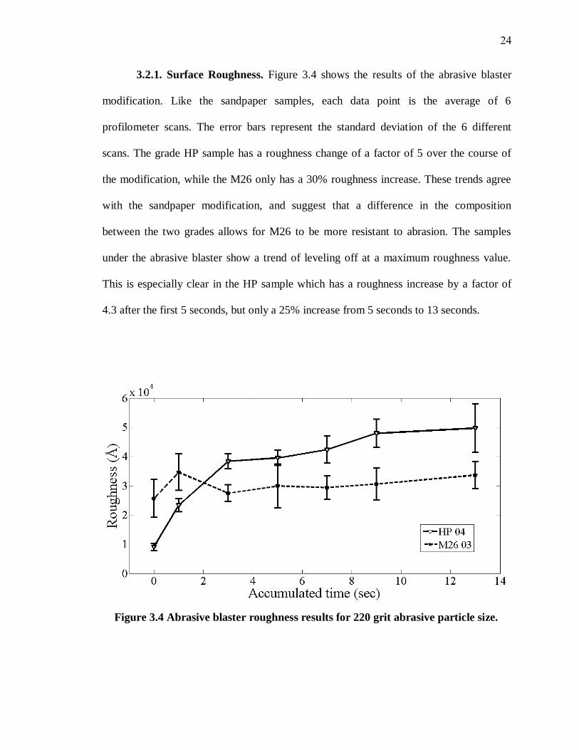
3.2.1. Surface Roughness. Figure 3.4 shows the results of the abrasive blaster
modification. Like the sandpaper samples, each data point is the average of 6
profilometer scans. The error bars represent the standard deviation of the 6 different
scans. The grade HP sample has a roughness change of a factor of 5 over the course of
the modification, while the M26 only has a 30% roughness increase. These trends agree
with the sandpaper modification, and suggest that a difference in the composition
between the two grades allows for M26 to be more resistant to abrasion. The samples
under the abrasive blaster show a trend of leveling off at a maximum roughness value.
This is especially clear in the HP sample which has a roughness increase by a factor of
4.3 after the first 5 seconds, but only a 25% increase from 5 seconds to 13 seconds.
Figure 3.4 Abrasive blaster roughness results for 220 grit abrasive particle size.
25
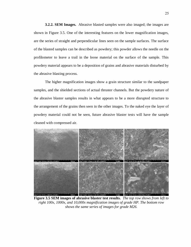
3.2.2. SEM Images. Abrasive blasted samples were also imaged; the images are
shown in Figure 3.5. One of the interesting features on the lower magnification images,
are the series of straight and perpendicular lines seen on the sample surfaces. The surface
of the blasted samples can be described as powdery; this powder allows the needle on the
profilometer to leave a trail in the loose material on the surface of the sample. This
powdery material appears to be a deposition of grains and abrasive materials disturbed by
the abrasive blasting process.
The higher magnification images show a grain structure similar to the sandpaper
samples, and the shielded sections of actual thruster channels. But the powdery nature of
the abrasive blaster samples results in what appears to be a more disrupted structure to
the arrangement of the grains then seen in the other images. To the naked eye the layer of
powdery material could not be seen, future abrasive blaster tests will have the sample
cleaned with compressed air.
Figure 3.5 SEM images of abrasive blaster test results. The top row shows from left to
right 100x, 1000x, and 10,000x magnification images of grade HP. The bottom row
shows the same series of images for grade M26.
26
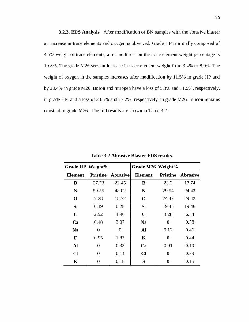
3.2.3. EDS Analysis. After modification of BN samples with the abrasive blaster
an increase in trace elements and oxygen is observed. Grade HP is initially composed of
4.5% weight of trace elements, after modification the trace element weight percentage is
10.8%. The grade M26 sees an increase in trace element weight from 3.4% to 8.9%. The
weight of oxygen in the samples increases after modification by 11.5% in grade HP and
by 20.4% in grade M26. Boron and nitrogen have a loss of 5.3% and 11.5%, respectively,
in grade HP, and a loss of 23.5% and 17.2%, respectively, in grade M26. Silicon remains
constant in grade M26. The full results are shown in Table 3.2.
Table 3.2 Abrasive Blaster EDS results.
Grade HP Weight% Grade M26 Weight%
Element Pristine Abrasive Element Pristine Abrasive
B 27.73 22.45 B 23.2 17.74
N 59.55 48.02 N 29.54 24.43
O 7.28 18.72 O 24.42 29.42
Si 0.19 0.28 Si 19.45 19.46
C 2.92 4.96 C 3.28 6.54
Ca 0.48 3.07 Na 0 0.58
Na 0 0 Al 0.12 0.46
F 0.95 1.83 K 0 0.44
Al 0 0.33 Ca 0.01 0.19
Cl 0 0.14 Cl 0 0.59
K 0 0.18 S 0 0.15
27
3.3. VACUUM HEATING
The anode at the base of the thruster channel can heat the channel wall to 400 C
based on the work by Tomaszewski, et al. [27]. The binder agent within the ceramic
composition of the BN material has a significantly lower melting point than the boron
nitride. Boric acid in the grade HP and silicon dioxide in the grade M26 melt at 550 C
and 1700 C, respectively. Changes in material composition at various locations in the
thruster have been observed by Zidar and Rovey [1-3]. These changes may be partially
related to heat, or if not, it may be possible to replicate the changes through the use of
heat treatments. Samples are heated in a Thermal Technology model 1100-4080-W3
furnace under high vacuum conditions. Temperatures of 400, 1000, and 1800 C are used
to modify BN samples. The 400 C temperature replicates the temperature conditions of a
running thruster [27]. The 1000 and 1800 C temperatures are chosen to study any effects
that might result from the loss of the binding agent in the ceramic. The samples are each
heated for 30 minutes.
3.3.1. Surface Roughness. Heat treated samples did not show a change in
surface roughness. Any surface changes that happen to the sample due to heating are on a
scale smaller than can be measured by the profilometer. The surface roughness of the
unmodified sample of M26 was 27,218 Å, and after heating the roughness was 26,704 Å,
well within the standard deviation of 3,117 Å seen on the pristine sample.
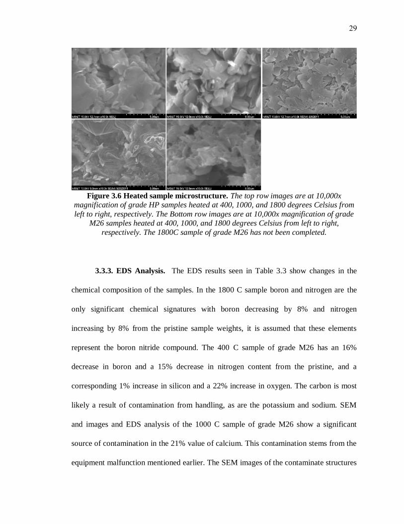
3.3.2. SEM Images. Images at the 10,000x magnification seen in Figure 3.6,
most clearly show changes in the microstructure. The HP sample heated to 1800 C looks
similar to the undisturbed sections of the other modified samples of grade HP. The

28
individual grains on the HP sample do appear more rounded at the corners than the grains
from the other methods of modification. The boundaries of the grains are also easily
identified with the loss of the binding agent. This gives the appearance of small grains
when in actuality the grains are the same size but more easily identified as individuals. In
the 400 C image, the grains of BN are still connected to each other to form larger plates
around 6 μm in size, where as in the 1800 C image, the grains of BN are separated from
each other by more fracture lines, resulting in grains of 2 μm in size. The sample of M26
heated to 400 C shows a layered pattern of flat grains stacked horizontally on each other.
This stacked pattern is not prominently displayed in the 1000 C sample. The 1800 C
sample of grade M26 was not able to be run with the other sample due to malfunctioning
equipment.
29
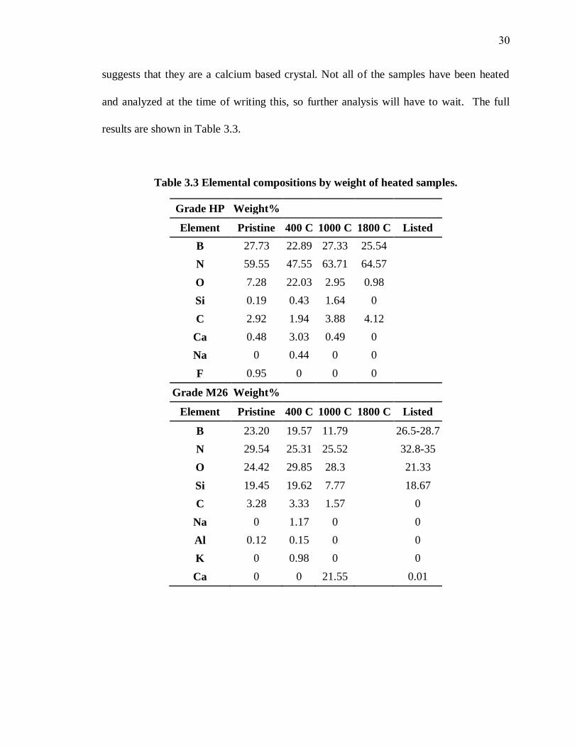
3.3.3. EDS Analysis. The EDS results seen in Table 3.3 show changes in the
chemical composition of the samples. In the 1800 C sample boron and nitrogen are the
only significant chemical signatures with boron decreasing by 8% and nitrogen
increasing by 8% from the pristine sample weights, it is assumed that these elements
represent the boron nitride compound. The 400 C sample of grade M26 has an 16%
decrease in boron and a 15% decrease in nitrogen content from the pristine, and a
corresponding 1% increase in silicon and a 22% increase in oxygen. The carbon is most
likely a result of contamination from handling, as are the potassium and sodium. SEM
and images and EDS analysis of the 1000 C sample of grade M26 show a significant
source of contamination in the 21% value of calcium. This contamination stems from the
equipment malfunction mentioned earlier. The SEM images of the contaminate structures
Figure 3.6 Heated sample microstructure. The top row images are at 10,000x
magnification of grade HP samples heated at 400, 1000, and 1800 degrees Celsius from
left to right, respectively. The Bottom row images are at 10,000x magnification of grade
M26 samples heated at 400, 1000, and 1800 degrees Celsius from left to right,
respectively. The 1800C sample of grade M26 has not been completed.
30
suggests that they are a calcium based crystal. Not all of the samples have been heated
and analyzed at the time of writing this, so further analysis will have to wait. The full
results are shown in Table 3.3.
Table 3.3 Elemental compositions by weight of heated samples.
Grade HP Weight%
Element Pristine 400 C 1000 C 1800 C Listed
B 27.73 22.89 27.33 25.54
N 59.55 47.55 63.71 64.57
O 7.28 22.03 2.95 0.98
Si 0.19 0.43 1.64 0
C 2.92 1.94 3.88 4.12
Ca 0.48 3.03 0.49 0
Na 0 0.44 0 0
F 0.95 0 0 0
Grade M26 Weight%
Element Pristine 400 C 1000 C 1800 C Listed
B 23.20 19.57 11.79 26.5-28.7
N 29.54 25.31 25.52 32.8-35
O 24.42 29.85 28.3 21.33
Si 19.45 19.62 7.77 18.67
C 3.28 3.33 1.57 0
Na 0 1.17 0 0
Al 0.12 0.15 0 0
K 0 0.98 0 0
Ca 0 0 21.55 0.01
31
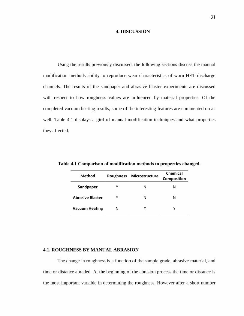
4. DISCUSSION
Using the results previously discussed, the following sections discuss the manual
modification methods ability to reproduce wear characteristics of worn HET discharge
channels. The results of the sandpaper and abrasive blaster experiments are discussed
with respect to how roughness values are influenced by material properties. Of the
completed vacuum heating results, some of the interesting features are commented on as
well. Table 4.1 displays a gird of manual modification techniques and what properties
they affected.
Table 4.1 Comparison of modification methods to properties changed.
Method Roughness Microstructure Chemical
Composition
Sandpaper Y N N
Abrasive Blaster Y N N
Vacuum Heating N Y Y
4.1. ROUGHNESS BY MANUAL ABRASION
The change in roughness is a function of the sample grade, abrasive material, and
time or distance abraded. At the beginning of the abrasion process the time or distance is
the most important variable in determining the roughness. However after a short number

32
of iterations of abrasion the time or distance becomes less important to the roughness
value compared to the effect of the grit used to modify the sample.
4.1.1. Time or Distance Independent Roughness. There appears to be a
limiting trend to the maximum roughness a sample can achieve from a given grit
abrasive, shown in Figure 4.1. To study this maximum roughness, samples are abraded
for roughly two times the maximum distance or time used in the incremented tests, this
means 20 seconds in the blaster, or 40 centimeters on the sandpaper. This excessive
duration of abrasion ensures that the maximum roughness value will have been met as
seen by the decreasing and plateauing slope between later data points in Figures 3.1 and
3.4.
Figure 4.1 Effect of grit number on maximum roughness results.

33
The graph in Figure 4.1 shows a decreasing roughness with increasing grit
number, as would be expected with smaller particles carrying less energy and therefore
causing less damage to the sample surface. Similar to the incremented sandpaper and
abrasive blaster tests, the M26 has a lower roughness for every grit number compared to
the grade HP. The sandpaper modifications show a more uniform trend of roughness to
grit than the abrasive blaster the scale of the abrasion damage and therefore the
corresponding roughness value is a function of impact particle size, speed, and angle of
incidence, as well as impacter material properties and surface material properties with the
specific relation of these variables still under investigation. The abrasive blaster has a
higher roughness at the higher grit values than the sandpaper. The higher roughness and
more non uniform trend, of the abrasive blaster test stems from how the grit application
method affects existing features on the sample surface. Tooling marks and macroscopic
surface features cause higher roughness values to be seen by the profilometer. The
abrasive blaster applies grit evenly across the entire surface area of the sample equally
roughing the peaks and valley of existing surface features like tool markings, while the
sandpaper abrasion gives emphasis to eroding the peaks of structures first resulting in a
more level surface after modification as the peaks of preexisting tooling marks are worn
down.
4.1.2. Importance of Grit. Apart from time or distance abraded at low numbers
of iterations of drags or blasts, the grit size of the abrasive has the strongest effect on the
roughness of the samples. Lower number grits result in higher roughness values. At the

34
60 grit abrasion the samples became more difficult to measure due to the size of the
features becoming close to the maximum difference the profilometer was capable of
measuring.
The method of application of the grit also shows some effect on the maximum
roughness. The abrasive blaster on average gives the samples a lower roughness than
sandpaper of the same grit at grit values above 220. This result is from the difference in
how the grit modifies the surface, and the force with which the grit is applied to the
sample surface. The sandpaper leaves long straight grooves in the surface as shown in the
left image of Figure 4.2 the groove runs the length of the sample surface and is roughly
150 μm wide. The abrasive blaster leaves small pits where the grit particles impact the
surface of the samples. The pits highlighted in Figure 4.2 appear to be the result of a
single particle impact of slightly over 200 μm in diameter, which is comparable to the
265 μm average particle size of a 60 grit particle. This allows a single particle of grit to
affect a significantly larger area of the sample under the sandpaper method as compared
to the abrasive blaster method. Affecting a larger area of the sample gives the feature a
much better chance of being detected by a profilometer pass.

35
4.1.3. Importance of Ceramic Grade. Throughout all of the abrasive tests the
grade M26 has a lower roughness for the same grit value than the grade HP. The
difference in the roughness suggests that the difference in chemical composition of the
grades has an effect on how the samples erode. The grade HP has boric acid as a binding
agent, where as M26 uses silicon dioxide as a binding agent. The use of different binding
agents has to account for the differences seen in the erosion of the two grades as all the
other variables in the abrasion tests were held constant.
4.2. SEM RESULTS DISCUSSION
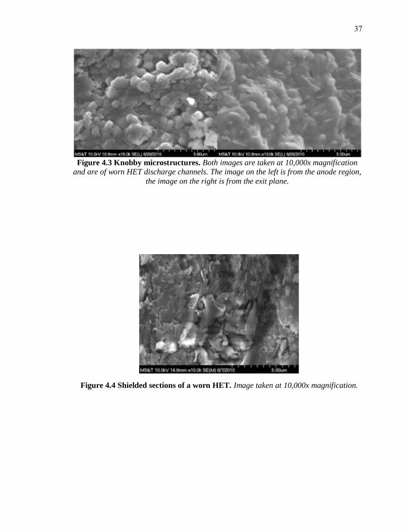
The SEM images show that although the numeric values of roughness could
match the actual thruster channels, the microstructures could not be replicated.
Specifically the knobby microstructures seen in 10,000x images of the actual thruster
Figure 4.2 Pits created by particle bombardment from 60 grit abrasive blaster. The
white line in the left image shows the peak to peak distance of a groove craved out by
sandpaper abrasion. The groove has a width of 150 μm and runs the length of the
sample surface. The white circles in the right image highlight pits caused by particle
impact. The distinguishable craters have a size range of 250 μm to 200 μm. Both
images are at 100x magnification.
36
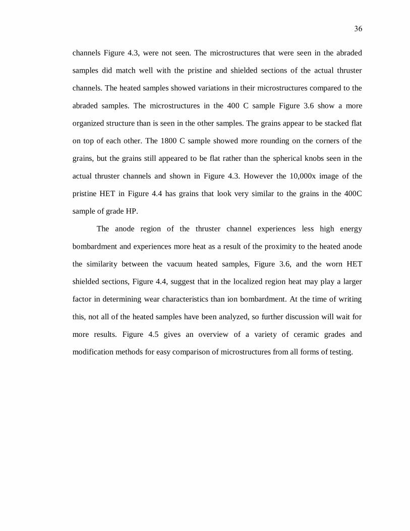
channels Figure 4.3, were not seen. The microstructures that were seen in the abraded
samples did match well with the pristine and shielded sections of the actual thruster
channels. The heated samples showed variations in their microstructures compared to the
abraded samples. The microstructures in the 400 C sample Figure 3.6 show a more
organized structure than is seen in the other samples. The grains appear to be stacked flat
on top of each other. The 1800 C sample showed more rounding on the corners of the
grains, but the grains still appeared to be flat rather than the spherical knobs seen in the
actual thruster channels and shown in Figure 4.3. However the 10,000x image of the
pristine HET in Figure 4.4 has grains that look very similar to the grains in the 400C
sample of grade HP.
The anode region of the thruster channel experiences less high energy
bombardment and experiences more heat as a result of the proximity to the heated anode
the similarity between the vacuum heated samples, Figure 3.6, and the worn HET
shielded sections, Figure 4.4, suggest that in the localized region heat may play a larger
factor in determining wear characteristics than ion bombardment. At the time of writing
this, not all of the heated samples have been analyzed, so further discussion will wait for
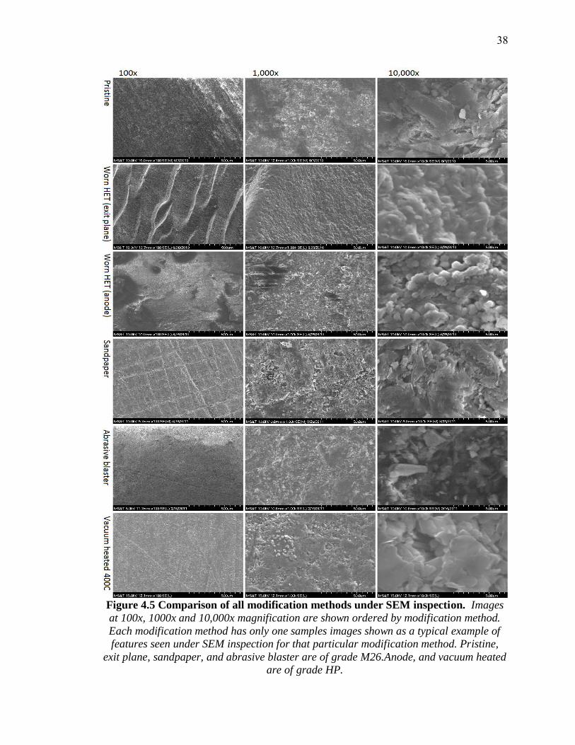
more results. Figure 4.5 gives an overview of a variety of ceramic grades and
modification methods for easy comparison of microstructures from all forms of testing.
37
Figure 4.4 Shielded sections of a worn HET. Image taken at 10,000x magnification.
Figure 4.3 Knobby microstructures. Both images are taken at 10,000x magnification
and are of worn HET discharge channels. The image on the left is from the anode region,
the image on the right is from the exit plane.
38
Figure 4.5 Comparison of all modification methods under SEM inspection. Images
at 100x, 1000x and 10,000x magnification are shown ordered by modification method.
Each modification method has only one samples images shown as a typical example of
features seen under SEM inspection for that particular modification method. Pristine,
exit plane, sandpaper, and abrasive blaster are of grade M26.Anode, and vacuum heated
are of grade HP.

39
4.3. EDS RESULTS DISCUSSION
EDS analysis was performed on samples from all of the manual modification
methods. All of the samples were coated with a gold palladium alloy for the SEM
imaging process. The results presented in all of the EDS analysis have had all gold and
palladium values withheld from the displayed results.
4.3.1. Abrasion Sample EDS. As expected of the abrasive modified samples,
after modification trace elements not present in the listed or pristine results appeared.
Aluminum is a result of the aluminum oxide grit used in both the abrasive blaster and on
the sandpaper. Potassium, sodium, calcium, carbon and chlorine are most likely deposited
when handling the samples in between abrasion and imaging.
Of particular interest was the nearly 10% increase in oxygen seen across all
grades and abrasion methods as compared to the pristine samples. The amount of extra
oxygen is great enough based on stoichiometric analysis that another source besides left
over abrasive aluminum oxide must be contributing oxygen to the sample. For example in
the grade M26 sandpaper abraded sample Table 3.2 has a 7.8% total weight of oxygen
not bound in the formation of silicon dioxide. Assuming all of the trace aluminum is used
the formation of aluminum oxide, the oxygen used only accounts for 3.1% of the extra
oxygen weight. Another source of oxygen is a thin film of B2O3 that can form on the
sample surface in the presence of air, as reported by Leichtfried et al. [30]. Using the
same grade M26 sample mentioned above, assuming a maximum yield of boron nitride
based on the EDS elemental weights once all of the nitrogen is used, there is still 1% of
the sample weight that is composed of boron not used in the formation of boron nitride.
This extra boron is likely to be the boron involved in the creation of B2O3, which

40
accounts for a further 2.4% of the extra oxygen weight. A further possible cause of the
extra oxygen may be due to the hygroscopic nature of boron nitride. The last 2.3% of
oxygen weight not accounted for by Al2O3 and B2O3 could be from water trapped in the
sample, keeping in mind that hydrogen cannot be seen through EDS analysis. With the
manual abrasion methods significantly increasing the surface area of the sample, a film of
B2O3 could account for a 30% of the increase in oxygen seen on the EDS results along
with contributions from other residual oxides, trapped water and from handling and
abrasive compound residues accounting for the rest of the increase.
4.3.2. Heated Sample EDS. The grade HP sample showed a loss of many of the
binding agent elements beginning at the 1000 C sample. The melting point of boric acid,
the primary binding agent in grade HP, is 550 C. Between the 400 C sample and the 1000
C sample the oxygen content goes from 22% to 3%. The 1800 C sample further supports
this conclusion with an oxygen amount of less than 1%. It is likely that the oxygen
present in the 1800 C sample is not from the original oxygen containing compounds in
the sample, but is from B2O3 contamination from the air after heating, as was seen on the
EDS of the abraded samples.
In comparison to the HP sample, the M26 sample shows a slight increase in SiO2,
with a corresponding decrease in boron nitride. These results are unexpected under the
assumption that SiO2 is the first part of the ceramic to be lost under heating conditions
given the melting temperature of boron nitride is 2900 C compared to the 1700 C melting
point of SiO2.
It should be noted that for each temperature level, a different sample had to be
used. This is a result of having to coat the samples in gold-palladium for use in the SEM.
41
While care was taken to ensure that all of the samples came from the same block of
material, inhomogeneities within the block could affect the local distribution of elements
in the sample.
4. CONCLUSION
Sandpaper and abrasive blaster modification methods have both shown the ability
to match the numerical roughness values seen at any location in a worn HET as measured
by Zidar, et al., [1-3] However the structures responsible for roughness values in worn
HET's look substantially different from the structures created by both methods of
abrasion. The recommended method to match a pristine samples surface roughness value
to a worn samples roughness value would be to choose a grit size based on the data in
Figure 4.1 that produces a maximum roughness after prolonged abrasion which matches
the worn roughness value.
Vacuum heating has shown an ability to modify the microstructures and chemical
composition of the samples. So far there appears to be a resemblance between the
shielded sections of the worn HET, and the heated samples microstructure. However
other microstructures seen in the worn HET have yet to be reproduced. Heating can be
used to modify the amount of binding agent in the BN samples, with a wider range of
heated data points it may be possible to replicate specific ratios of boron nitride to
binding agent seen at different locations in the worn HET.
42
REFERENCES
[1] Zidar, D. G., “Hall-effect Thruster Surface Properties Investigation,” Masters
Thesis, Dept. of Aerospace Engineering, Missouri University of Science &
Technology, Rolla, MO, 2011.
[2] Zidar, D. G., Rovey, J. L., “Boron Nitride Hall-effect Thruster Channel Surface
Properties Investigation,” AIAA-2011-5993, 47th Joint Propulsion Conference,
San Diego, CA, July 31 - Aug 3, 2011.
[3] Zidar, D. G., Rovey, J. L., “Hall-effect Thruster Channel Surface Properties
Investigation,” Journal of Propulsion and Power, accepted 9/2011.
[4] Fife, J. M., Gibbons, M. R., Hargus, W. A., VanGilder, D. B. and Kirtley, D. B.,
“3-D Computation of Surface Sputtering and Redeposition Due to Hall Thruster
Plumes,” International Electric Propulsion Conference, IEPC, 2003.
[5] Hofer, R. R., Mikellides, I. G., Katz, I. and Goebel, D. M.,”Wall Sheath and
Electron Mobility Modeling in Hybrid-PIC Hall Thruster Simulations,” 43rd
AIAA/ASME/SAE/ASEE Joint Propulsion Conference and Exhibit, AIAA, 2007.
[6] Ivanov, A. A., Ivanov Jr., A. A. and Bacal, M.,”Effect of plasma-wall
recombination on the conductivity of Hall thrusters,” Plasma Physics and
Controlled Fusion, Vol. 44, No. 7, 2002, pp. 1463-1470.
[7] Sommier, E., Allis, M. K., Gascon, N. and Cappelli, M. A.,”Wall Erosion in 2D
Hall Thruster Simulations,” 42nd
AIAA/ASME/SAE/ASEE Joint Propulsion
Conference and Exhibit, AIAA, 2006.
[8] Sullivan, K., Fox, J., Martinez-Sanchez, M. and Batischev, O.,”Kinetic Study of
Wall Effect in SPT Hall Thrusters,” 40th
AIAA/ASME/SAE/ASEE Joint Propulsion
Conference and Exhibit, AIAA, 2004.
[9] Locke, S., Shumlak, U. and Fife, J. M.,”Effect of a Channel Wall Discontinuity in
an SPT-Type Hall Thruster,” 37th AIAA/ASME/SAE/ASEE Joint Propulsion
Conference, AIAA, 2001.
[10] Morozov, I A.,”The Conceptual Development of Stationary Plasma Thrusters,”
Plasma Physics Reports, Vol. 29, No. 3, 2003, pp. 235-250. (Translated from
Russian. Originally published in Fizika Plazmy, Vol 29, No, 3,pp. 261-276.)
[11] Raitses, Y., Staack, D., Keidar, M. and Fisch, N. J.,”Electron-wall interaction in
Hall thrusters,” Physics of Plasmas, Vol. 12.No. 5, 2005, pp. 057104-1 – 057104-
9.
[12] Dunaevsky, A., Raitses, Y. and Fisch, N. J.,”Secondary electron emissions from
dielectric materials of a Hall thruster with segmented electrodes,” Physics of
Plasmas, Vol. 10, No. 6, 2003, pp. 2574-2577.
43
[13] Raitses, Y., Smirnov, A., Staack, D. and Fisch, N. J.,”Measurements of secondary
electron emission effects in the Hall thruster discharge,” Physics of Plasmas, Vol.
13, No. 1, 2006, pp. 014502-014502-4.
[14] Peterson, P. Y., Jacobson, D. T., Manzella, D. H. and John, J. W.,”The
Performance and Wear Characterization of a High-Power High-Isp NASA Hall
Thruster,” 41st AIAA /ASME/SAE/ASEE Joint Propulsion Conference and
Exhibit, AIAA, 2005.
[15] Mason, L. S., Jankovsky, R. S. and Manzella, D. H.,”1000 Hours of Testing on a
10 Kilowatt Hall Effect Thruster,” 37th AIAA /ASME/SAE/ASEE Joint Propulsion
Conference and Exhibit, AIAA, 2001.
[16] Gorschkov, O., Shagayda, A. and Muravlev, V.,”The Experience of Hall Thruster
Research and Development,” 57th International Astronautical Congress, IAC,
2006. pp. 1-8.
[17] de Grys, K., Mathers, A., Welander, B. and Khayms, V.,”Demonstration of
10,400 Hours of Operation on a 4.5 kW Qualification Model Hall Thruster, “46th
AIAA/ASME/SAE/ASEE Joint Propulsion Conference &Exhibit, AIAA, 2010.
[18] Sydorenko, D., Smolyakov, A., Kaganovich, I. and Raitses, Y., “Kinetic
Simulation of Effects of a Secondary Electron Emission on Electron Temperature
in Hall Thrusters,” The 29th Annual International Electric Propulsion
Conference, IEPC,2005.
[19] Zhurin, V. V., Kaufman, H. R. and Robinson, R. S., “Physics of closed drift
thrusters,” Plasma Sources Science and Technology, Vol. 8, No. 1, 1999, pp. R1-
R20.
[20] Choueiri, E. Y., “Fundamental Difference Between the Two Hall Thruster
Variants,” Physics of Plasmas, Vol. 8, No. l, 2001, pp. 5025-5033.
[21] Gascon, N., Dudeck, M. and Barral, S.,”Wall material effects in stationary plasma
thrusters. I. Parametric studies of an SPT-100,” Physics of Plasmas, Vol. 10, No.
10, 2003, pp. 4123-4136.
[22] Yong, Y. C., Thong, J. T. L. and Phang, J. C. H.,”Determination of secondary
electron yield from insulators due to a low-kV electron beam,” Journal of Applied
Physics, Vol. 84, No. 8, 1998, pp. 4543-4548.
[23] Garnier, Y., Viel, V., Roussel, J. F. and Bernard, J.,” Low-energy xenon ion
sputtering of ceramics investigated for stationary plasma thrusters,” Journal of
Vacuum Science and Technology, Vol. 17, No. 6, 1999, pp. 3246-3254.
[24] Garnier, Y., Viel, V., Roussel, J. F., Pagnon, D., Mange, L. and Touzeau,
M.,”Investigation of Xenon Ion Sputtering of One Ceramic Material Used in SPT
Discharge Chamber,” 26th International Electric Propulsion Conference, IEPC,
1999, pp. 512-517.
[25] Tondu, Th., Viel-Inguimbert, V., Roussel, J. F. and D'Escrivan, S.,”Hall Effect
Thrusters ceramics sputtering yield determination by Monte Carlo simulations,”
44th AIAA/ASME/SAE/ASEE Joint Propulsion and Exhibit , AIAA, 2008.
44
[26] Peterson, P. Y. and Manzella, D. H.,”Investigation of the Erosion Characteristics
of a Laboratory Hall Thruster,” 39th AIAA/ASME/SAE/ASEE Joint Propulsion
Conference and Exhibit, AIAA, 2003.
[27] Tomaszewski, James, et al., “Characterization of a Hall Effect Thruster Using
Thermal Imaging,” 45th AIAA Aerospace Sciences Meeting and Exhibit, Reno,
NV, 2007, AIAA 2007-0584.
[28] Sloan Technology Corporation, Dektak IIA Manual, Sloan Technology
Corporation, Santa Barbara, CA, 1984, p. i.
[29] —. CombatR Solid Boron Nitride Composite Grade HP. [Online] February 2006.
[Cited: September 9, 2010.]http://www.bn.saint-
gobain.com/uploadedFiles/SGbn/Documents/Solids/Solid-Combat-BN-
GradeHP.pdf.
[30] —. CombatR Solid Boron Nitride Composite Grades M and M26. [Online] June
2003. [Cited: September 9, 2010.] http://www.bn.saint-
gobain.com/uploadedFiles/SGbn/Documents/Solids/Solid-Combat-GradesM-
M26.pdf.
[31] Goldstein, J. I., Newbury, D. E., Echlin, P., Joy, D. C., Romig, Jr., A. D., Lyman,
C. E., Fiori, C. and Lifshin, E., Scanning Electron Microscopy and X-ray
Microanalysis. 2nd edition, Plenum Press, New York. 1992. pp. 21-25,292-311.
[32] P. Beiss, G. Leichtfried et al. (2002). “13.5 Properties of diamond and cubic
boron nitride”. Landolt-Bornstein– Group VIII Advanced Materials and
Technologies: Powder Metallurgy Data. Refractory, Hard and Intermetallic
Materials. 2A2. Berlin: Springer. pp. 118– 139. doi:10.1007/b83029. ISBN 978-
3-540-42961-6.
45
PAPER
II. Plasma Exposure of Hall Effect Thruster Ceramic Material
Alexander J. Satonik, Joshua L. Rovey, and Greg Hilmas
Missouri University of Science and Technology, Rolla, MO, 65409
ABSTRACT
Worn Hall effect thrusters show a variety of unique microstructures and elemental
compositions in the boron nitride thruster channel walls. Understanding the plasma
conditions that lead to the formation of these microstructures and elemental changes can
assist in the goal of creating new ceramic materials with desired plasma material
interactions. Pristine, abraded and worn HET thruster channel samples of boron nitride
were exposed to a xenon plasma in a magnetron sputter device. The samples were
characterized before and after plasma exposure. Erosion rate was shown to depend on
the grade of the BN ceramic and the preparation of the surface prior to plasma exposure.
Abraded samples were shown to erode 43% more than their pristine counterparts.
Unique surface features and elemental compositions on the worn thruster channel
samples were overwritten by new surface features which include terraced steps on the
ceramic grains, and pools of silicon dioxide created by the magnetron plasma. The

46
microscope images of the ceramic surface show that the magnetron plasma source
rounded the edges of the ceramic grains to closely match the worn HET surface. This
effect was not as pronounced in studies of ion beam bombardment of the surface and
appears to be a result of the quasi-neutral plasma environment.
NOMENCLATURE
E = Electric field
B = Magnetic field
Ra = Roughness value
1. INTRODUCTION
Hall effect thrusters (HETs) are an electric spacecraft propulsion system in which
thrust generation is due to acceleration of ionized propellant called plasma. Typically, an
HET has an annular geometry in which an axial electric field is crossed with a radial
magnetic field. A cathode emits electrons that drift in the direction, forming an
azimuthal Hall current. Neutral propellant atoms, typically xenon, are injected through
the anode into an annular insulating channel. Collisions between neutral xenon atoms and
electrons drifting in the Hall current produce xenon ions that are accelerated by the
electric field, resulting in thrust generation.
47
Many current HET efforts are focused on developing and benchmarking models
that integrate the important role of surface properties of the annular channel that contains
the plasma discharge [1-8]. Wall-effects play an important role in both the lifetime and
overall performance of the thruster. Properties of the channel wall can affect secondary
electron emission (SEE), anomalous electron transport, and near-wall conductivity,
thereby altering HET performance [9-13]. Further, wall properties are an important factor
in the sputter erosion processes that are known to limit thruster lifetime [14-18]. Current
HET models do not integrate a realistic wall microstructure, but instead rely on sputter
yield or SEE coefficients derived from idealized material tests [1,6,18].
Properties of the HET channel wall affect SEE, anomalous electron transport,
near-wall conductivity, and erosion rate, thereby altering HET performance [9,19]. The
roughness of HET channel walls has been shown to affect the equipotential contours of
the plasma sheath near the channel wall reducing overall thruster performance [20].
Raitses, et al., show that wall materials having higher SEE reduce the electron
temperature within the HET discharge channel, thereby reducing thruster performance
[10,20]. Determining the influence of material surface properties on SEE in HETs is
difficult due to the complexity of electron-wall interaction, which must include factors
such as roughness, composition, non-Maxwellian electron distribution, and multiple
electron scattering processes all of which influence SEE yield, and as such have some
level of influence on HET performance [2]. The sputter yield (atoms removed per
incident ion) of the ceramic surface of a typical HET channel wall has been found to be
dependent upon the roughness of the ceramic surface [18,21,22].
48
The surface properties of the HET discharge channel change due to thruster
operation. Previous results have shown that the boron nitride (BN) channel surface
changes considerably after a few 100 hours of operation [1]. Zidar and Rovey compared
pristine and worn grade HP and M26 boron nitride channel material from various
locations within HETs and showed that surface changes occur on multiple length scales
and vary depending on the location in the channel [14] At the macroscopic level, surface
roughness increases, especially near the exit plane where angled striations in the channel
are formed. Near the anode, deposition of metallic materials was evident [14] At the
microscopic level, metallic atoms are deposited on the BN channel close to the anode and
individual BN grains become smoother. Both Garnier, et al., [21,22] and Zidar, et al.,
[14] showed that the chemical composition of the BN channel surface changes, with the
fraction of silicon dioxide binding agent decreasing with proximity to the exit plane of
the thruster. It is currently unclear how these surface changes affect SEE and sputter
yield, and indirectly affect performance and lifetime. Further it is unclear which changes
are unique to the HET and which are due to more general plasma exposure.
The goals of this study were to determine which changes are unique to HETs and
to study the effect of surface properties on sputter yield. Additionally, this study was
able to use controlled techniques to replicate some of the surface properties evident on
worn HET material. Understanding the origin and patterns of surface changes seen on
HETs may aid the creation of new materials with designed desired plasma-surface
interactions, a major national effort within the propulsion materials community. In the
following sections the results of plasma exposure of BN samples from worn HET thruster
channels, and pristine and manually modified BN of different grades are presented.
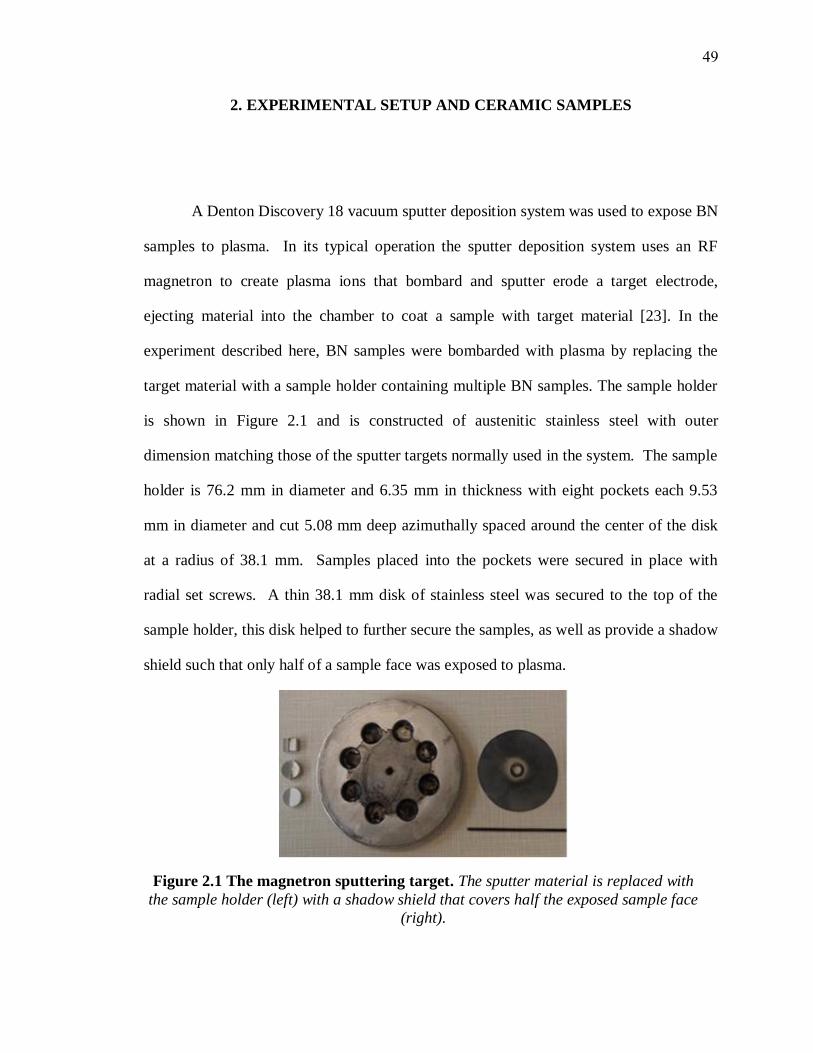
49
2. EXPERIMENTAL SETUP AND CERAMIC SAMPLES
A Denton Discovery 18 vacuum sputter deposition system was used to expose BN
samples to plasma. In its typical operation the sputter deposition system uses an RF
magnetron to create plasma ions that bombard and sputter erode a target electrode,
ejecting material into the chamber to coat a sample with target material [23]. In the
experiment described here, BN samples were bombarded with plasma by replacing the
target material with a sample holder containing multiple BN samples. The sample holder
is shown in Figure 2.1 and is constructed of austenitic stainless steel with outer
dimension matching those of the sputter targets normally used in the system. The sample
holder is 76.2 mm in diameter and 6.35 mm in thickness with eight pockets each 9.53
mm in diameter and cut 5.08 mm deep azimuthally spaced around the center of the disk
at a radius of 38.1 mm. Samples placed into the pockets were secured in place with
radial set screws. A thin 38.1 mm disk of stainless steel was secured to the top of the
sample holder, this disk helped to further secure the samples, as well as provide a shadow
shield such that only half of a sample face was exposed to plasma.
Figure 2.1 The magnetron sputtering target. The sputter material is replaced with
the sample holder (left) with a shadow shield that covers half the exposed sample face
(right).

50
Two different BN grades, with three different modification types were used in this
investigation. Pristine, manually modified, and worn types of grade HP and M26 were
investigated. Pristine samples of grades HP and M26 were cut from stock provided by
Saint Gobain Ceramics. Manually modified samples were prepared by abrading the
samples with 120 grit sandpaper. These manual modifications are known to alter the
microstructure and roughness of the sample and are used to isolate the effects of
temperature and roughness from worn sample results [15]. Sandpaper abraded samples
had a pre-plasma exposure surface roughness of 5.91x10⁴Å for grade M26, 8.51x10
4Å
for grade HP. These roughness levels are typical of a worn HET and range from 1.25 to 2
times larger than the pristine samples depending on ceramic grade.
Worn samples were cut from the same locations and the same two worn HET
channels studied by Zidar [14] These included samples from the grade M26 thruster
channel from both the inner and outer wall, and one sample from the grade HP channel
which included both the anode and exit plane sections of the thruster channel. Table 2.1
describes the different types of samples and different grades of BN that were
investigated.
Table 2.1 Boron nitride sample matrix.
Grade
Type HP
M26
Pristine X X
Manually Modified
Abraded X X
Worn
Anode X X
Middle - X
Exit Plane X X
Shielded - X
51
Two grades of BN were studied. Each grade has a different elemental
composition due to the type of binding agent used. The BN in each grade has a
hexagonal structure and the elemental composition of the investigated grades is shown in
Table 2.2 [24-27] Samples of boron nitride were machined into 9.5-mm-diameter, 3.2-
mm-thick disks, or squares of the same thickness whose dimensions can be circumscribed
into those of the disks. In preparation for plasma exposure half of the sample surface was
covered with a layer of kapton tape. The section of the sample covered in kapton was
oriented such that the kapton was covered by the shadow shield shown in Figure 2.1. All
BN samples were exposed to 4 hours of plasma bombardment, with the magnetron set to
80 W at 1000 V. Xenon gas was injected into the chamber to maintain a constant
pressure of 2x10⁻⁵
Torr.
Table 2.2 Weight ratios of BN and binder chemicals in the different grades
investigated.
Grade BN (%) SiO2 (%) B2O3 (%) B(OH)3 (%) Ca (%)
HP 92 - 0.3 4.6 3
M26 60 40 - - -
3. SAMPLE CHARACTERIZATION METHODS
Samples are characterized using surface profilometry, Scanning Electron
Microscopy (SEM), X-ray Photoelectron Spectroscopy (XPS), and Energy Dispersive
Spectroscopy (EDS). Surface profilometry determines surface roughness by measuring
52
the height of finely spaced irregularities. Quantitatively, surface roughness is measured as
the height of surface irregularities with respect to an average line. Roughness is expressed
in units of length; in the case of this study, roughness is expressed in Angstroms. In this
investigation, roughness, termed Ra, is determined using the arithmetical average, as
defined in Eqn. 1:
(1)
For this investigation, surface profilometry is performed using a Sloan Dektak IIA
surface measuring system. The Dektak IIA is capable of measuring surface features
having heights ranging from less than 100 Å to 655,000 Å [28]. Calibration and
verification of accurate roughness measurements are conducted both before and after the
roughness studies performed using this instrument. In all cases the profilometer is found
to be accurate within the specified ±5% for all standards measured, which covered the
specified measurement range from 100 Å to 655,000 Å [28]. Scanning electron
microscope images of the tracks made by the scanning stylus of the profilometer
demonstrate that the profilometer stylus tip has a characteristic width of 10-15 μm [14].
The geometry of the stylus tip is assumed to be approximately hemispherical. The
characteristic width of the stylus tip constrains the size of the surface features which can
be measured in the direction of travel of the stylus tip. Therefore the profilometer can
make vertical measurements of surfaces having characteristic heights in the range of

53
100’s of Å, while the measurements of the horizontal lengths of these features are limited
to 10’s of μm. This model profilometer is a single line profilometer, meaning the
roughness can only be measured along a single line on the sample surface. To better
ensure that the roughness measurements reflect the roughness of an entire sample surface,
multiple scans were taken at multiple locations.
A Hitachi S-4700 scanning electron microscope was used to image the surface of
each sample. It is capable of producing images with magnification greater than 500,000
times, and can resolve structures up to 2 nm across. For this investigation, micrographs
were taken of each sample at magnifications of 30, 100, 1,000, and 10,000 times.
The SEM used in this investigation has energy dispersive x-ray spectroscopy
(EDS) capability. EDS is a variant of x-ray fluorescence spectroscopy, and is used for
chemical characterization and elemental analysis. A histogram of the emission spectrum
from the sample is obtained and analyzed to determine the percent by weight of elements
present in the sample. For this study, EDS analysis was conducted using an EDAX
energy dispersive x-ray unit attached to the Hitachi S4700 SEM. Data provided by EDS
yield the chemical composition of the sample regions by both percent of atoms and
percent by weight. This yield is taken from a volume proportional to the size of the x-ray
beam, and has characteristic penetration depth of 25 nm [29].
X-ray photoelectron spectroscopy (XPS) was used to study the elemental
composition of the surface of the eroded samples. As compared to EDS, XPS acquires
data form only the top 10 nm of the surface [29]. As part of the XPS measurements, the
sample surface was sputter cleaned for 30 seconds to remove trace contaminates allowing
for a better signal quality. Measurements were taken both after this sputter cleaning. The

54
measurements before sputter cleaning had high levels of carbon contamination, upwards
of 40% of the sample weight. The post cleaning data had values of carbon closer to what
had been seen in the EDS measurements. It is important to note that while the X-ray
beam can penetrate several micrometers into the surface of a sample, electrons emitted
deeper in the sample are recaptured within the sample material, thus only electrons on the
very top of the surface escape into the vacuum where they can be detected [29].
4. RESULTS
After plasma exposure, samples were characterized with the instruments
described above in order to study the amount of sputter erosion, chemical changes caused
by sputtering, and changes in the microstructure of the samples.
4.1. STEP HEIGHT
To quantify the erosion of the BN samples the size of the step height between the
plasma eroded region and shielded region was measured. The step height measurement is
used as a metric to determine the relative amount of sputter erosion of the different
samples since all samples were exposed to identical plasma for the same amount of time.
While the relative amount of erosion can be compared between samples with this step
height method, a measurement of total material lost is impractical due to the lack of a
micro balance in the sputter system vacuum facility. Weighing samples before and after

55
sputtering would not produce meaningful results due in part to the hygroscopic nature of
BN and deposition of metals and tape residue from the sputter process [30].
All of the measured samples showed a similar erosion profile, with a step at the
shadow shield boundary at the center of the sample. To reduce error due to unleveled
faces on the eroded surface, the step height was taken as the average height of the region
just below and just above the step at three separate locations across the face, and the
average value was calculated.
Step height results for pristine and manually modified BN samples are shown in
Figure 4.1. Pristine BN samples showed only small differences in eroded material.
Samples that had been manually modified through sandpaper abrasion all show more
erosion than the pristine samples of the same grade. Pristine grade HP had the lowest
erosion. Grade M26 had the largest change in erosion between the pristine and sandpaper
modified samples, with an increase in step height of 51%, from a step height of 186411 Å
to 379541 Å, followed by grade HP with an increase of 34%, from a step height of
194576 Å to 295460 Å. The error bars represent one standard deviation.
Figure 4.1 Step height of pristine and manually modified BN samples after plasma
exposure.
0
100000
200000
300000
400000
500000
Pristine Abraded
Ste
p H
eight
Å
Grade M26
Grade HP
56
The step height of worn HET samples is shown in Figure 4.2. The samples from
the HETs showed more erosion based on their larger step height than the pristine samples
of the same ceramic grades. Samples of M26 from the worn HET showed only small
variations in step height (< 7%) between samples from different locations in the thruster.
The sample from the exit-plane region of the thruster had the smallest step height with a
value of 214318 Å. The largest step height was found in the sample from the middle of
the thruster with a value of 244985 Å. Grade HP samples for the worn HET showed
significant differences in step height. The step height of the exit plane was 58% greater
than the pristine sample, and the step height of the anode region sample was 47% greater
than the pristine sample of grade HP.
Figure 4.2 Step height of worn thruster samples after plasma exposure.
0
100000
200000
300000
400000
500000
600000
1
Ste
p H
eig
ht
Å
M26 Shielded
M26 Anode
M26 Middle
M26 Exit Plane
HP Anode
HP Exit Plane
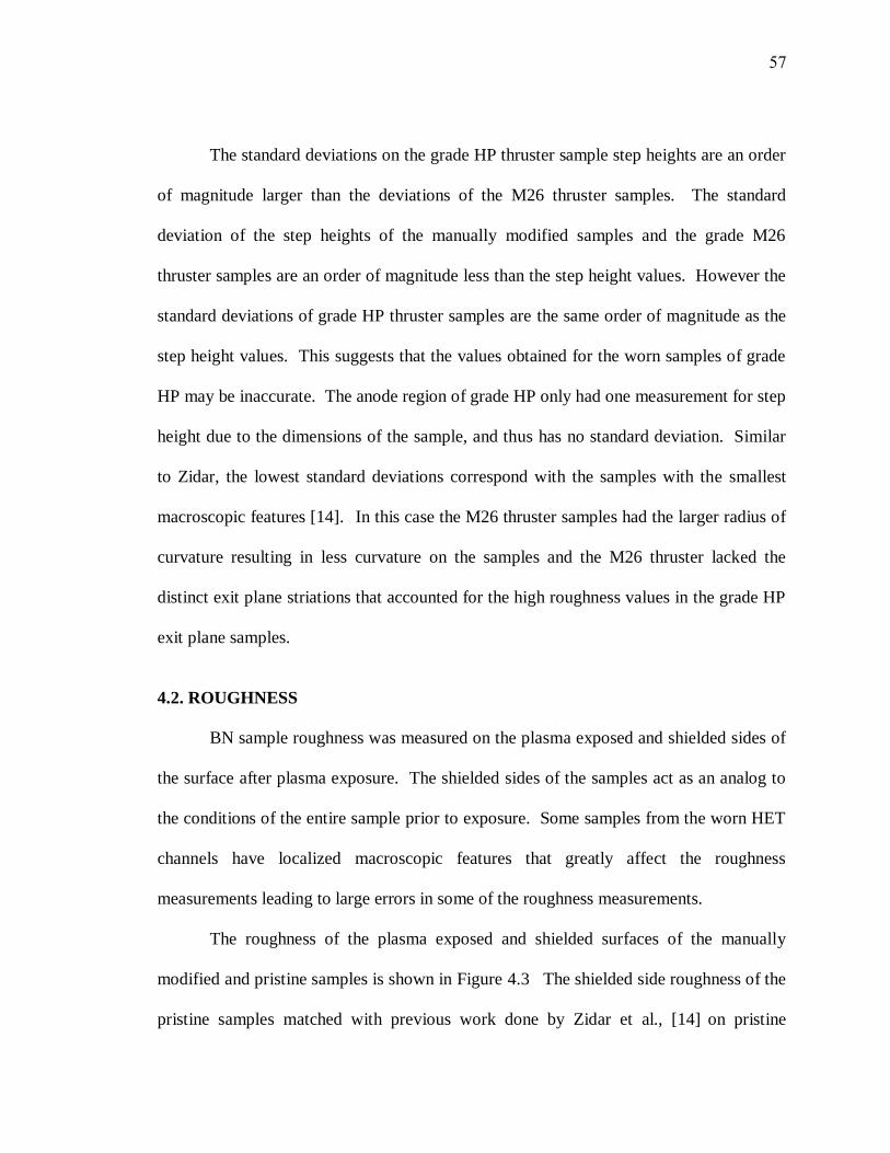
57
The standard deviations on the grade HP thruster sample step heights are an order
of magnitude larger than the deviations of the M26 thruster samples. The standard
deviation of the step heights of the manually modified samples and the grade M26
thruster samples are an order of magnitude less than the step height values. However the
standard deviations of grade HP thruster samples are the same order of magnitude as the
step height values. This suggests that the values obtained for the worn samples of grade
HP may be inaccurate. The anode region of grade HP only had one measurement for step
height due to the dimensions of the sample, and thus has no standard deviation. Similar
to Zidar, the lowest standard deviations correspond with the samples with the smallest
macroscopic features [14]. In this case the M26 thruster samples had the larger radius of
curvature resulting in less curvature on the samples and the M26 thruster lacked the
distinct exit plane striations that accounted for the high roughness values in the grade HP
exit plane samples.
4.2. ROUGHNESS
BN sample roughness was measured on the plasma exposed and shielded sides of
the surface after plasma exposure. The shielded sides of the samples act as an analog to
the conditions of the entire sample prior to exposure. Some samples from the worn HET
channels have localized macroscopic features that greatly affect the roughness
measurements leading to large errors in some of the roughness measurements.
The roughness of the plasma exposed and shielded surfaces of the manually
modified and pristine samples is shown in Figure 4.3 The shielded side roughness of the
pristine samples matched with previous work done by Zidar et al., [14] on pristine
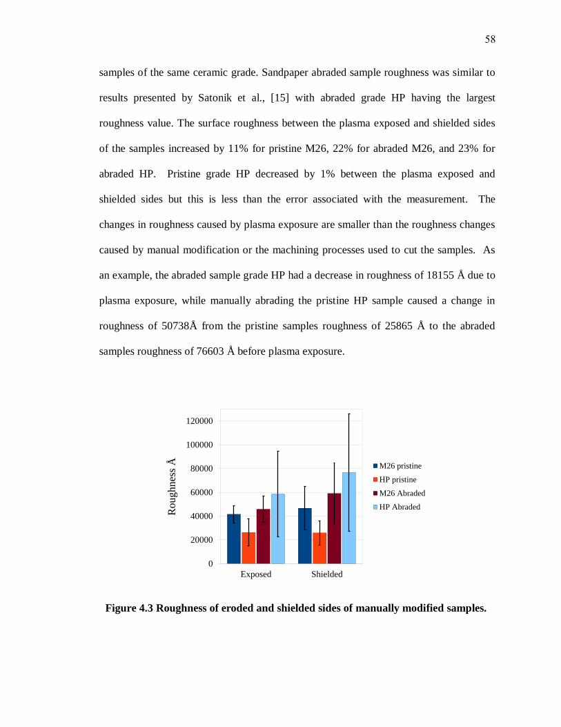
58
samples of the same ceramic grade. Sandpaper abraded sample roughness was similar to
results presented by Satonik et al., [15] with abraded grade HP having the largest
roughness value. The surface roughness between the plasma exposed and shielded sides
of the samples increased by 11% for pristine M26, 22% for abraded M26, and 23% for
abraded HP. Pristine grade HP decreased by 1% between the plasma exposed and
shielded sides but this is less than the error associated with the measurement. The
changes in roughness caused by plasma exposure are smaller than the roughness changes
caused by manual modification or the machining processes used to cut the samples. As
an example, the abraded sample grade HP had a decrease in roughness of 18155 Å due to
plasma exposure, while manually abrading the pristine HP sample caused a change in
roughness of 50738Å from the pristine samples roughness of 25865 Å to the abraded
samples roughness of 76603 Å before plasma exposure.
Figure 4.3 Roughness of eroded and shielded sides of manually modified samples.
0
20000
40000
60000
80000
100000
120000
Exposed Shielded
Ro
ug
hn
ess
Å M26 pristine
HP pristine
M26 Abraded
HP Abraded
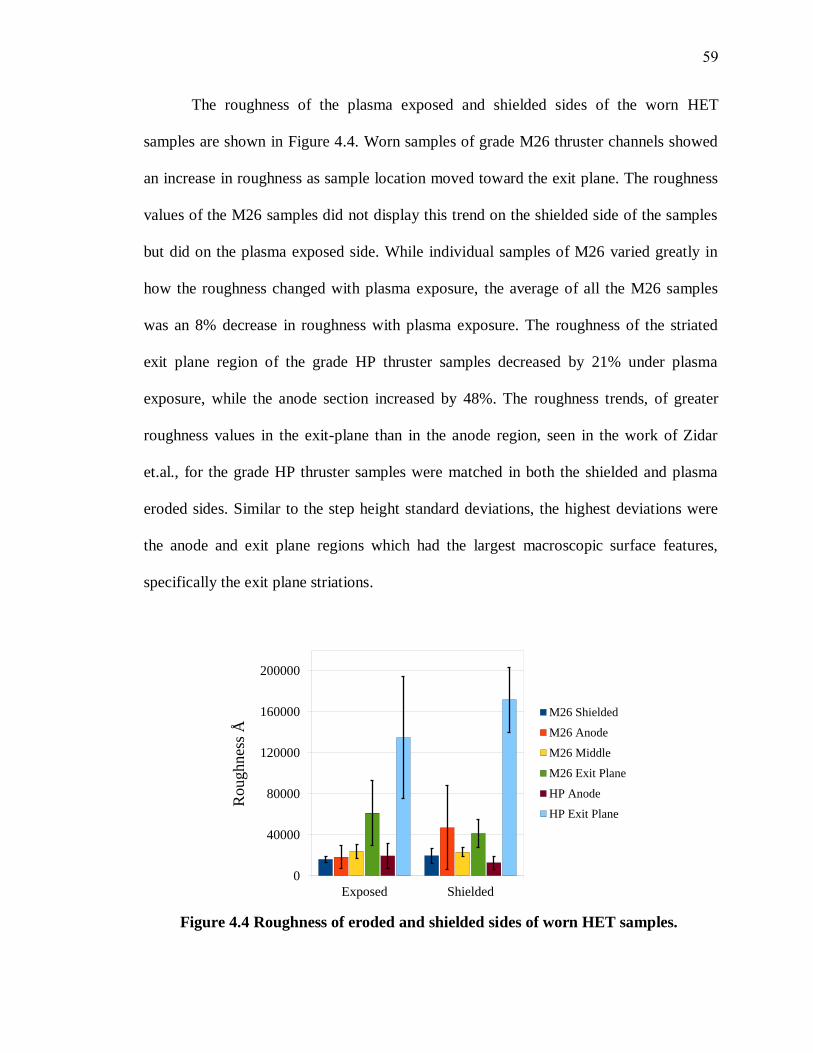
59
The roughness of the plasma exposed and shielded sides of the worn HET
samples are shown in Figure 4.4. Worn samples of grade M26 thruster channels showed
an increase in roughness as sample location moved toward the exit plane. The roughness
values of the M26 samples did not display this trend on the shielded side of the samples
but did on the plasma exposed side. While individual samples of M26 varied greatly in
how the roughness changed with plasma exposure, the average of all the M26 samples
was an 8% decrease in roughness with plasma exposure. The roughness of the striated
exit plane region of the grade HP thruster samples decreased by 21% under plasma
exposure, while the anode section increased by 48%. The roughness trends, of greater
roughness values in the exit-plane than in the anode region, seen in the work of Zidar
et.al., for the grade HP thruster samples were matched in both the shielded and plasma
eroded sides. Similar to the step height standard deviations, the highest deviations were
the anode and exit plane regions which had the largest macroscopic surface features,
specifically the exit plane striations.
Figure 4.4 Roughness of eroded and shielded sides of worn HET samples.
0
40000
80000
120000
160000
200000
Exposed Shielded
Ro
ug
hn
ess
Å
M26 Shielded
M26 Anode
M26 Middle
M26 Exit Plane
HP Anode
HP Exit Plane

60
4.3. ELEMENTAL COMPOSITION
All of the BN samples had EDS performed on the exposed and shielded sides.
Results for manually modified samples are shown in Table 4.1 M26 and HP grade worn
thruster sample results are shown in Table 4.2 and Table 4.3, respectively. The most
obvious result is the deposition of stainless steel from the sample holder evident on every
eroded sample. Most samples had between 2% and 5% elemental weight of iron and
0.5% to 1% chromium by weight. All of the exposed samples also contained trapped
xenon gas from a minimum of 3% to a high of 6%, while most samples had around 5%
xenon by weight. Trace amounts of sodium, chlorine, fluorine, potassium, and various
metals were seen on many samples, but all in weight concentrations less than 0.5%.
Table 4.1 shows the EDS and XPS results of both the shielded and plasma
exposed sides of the pristine and manually modified samples. The plasma exposed
samples all have new elements present in the surface chemistry from the embedded
xenon and deposited iron and chromium from the stainless steel. Both pristine and
abraded grade HP and pristine grade M26 had lower amounts of boron and nitrogen in
the plasma exposed sides as compared to the shielded sides, 18%, 4%, and 0.5% lower,
respectively. The abraded sample of grade M26 had an increase in BN on the plasma
exposed side of 12% compared to the shielded side. Silicon and oxygen decreased in
both of the M26 samples by 11% and 20% compared with the shielded side in the pristine
and abraded samples, respectively. This loss of silicon and oxygen under plasma
exposure corresponds well with the theory that more weakly bonded compounds are
preferentially eroded under plasma bombardment [31].
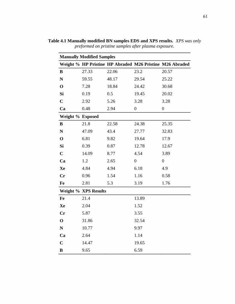
61
Table 4.1 Manually modified BN samples EDS and XPS results. XPS was only
preformed on pristine samples after plasma exposure.
Manually Modified Samples
Weight % HP Pristine HP Abraded M26 Pristine M26 Abraded
B 27.33 22.06 23.2 20.57
N 59.55 48.17 29.54 25.22
O 7.28 18.84 24.42 30.68
Si 0.19 0.5 19.45 20.02
C 2.92 5.26 3.28 3.28
Ca 0.48 2.94 0 0
Weight % Exposed
B 21.8 22.58 24.38 25.35
N 47.09 43.4 27.77 32.83
O 6.81 9.82 19.64 17.9
Si 0.39 0.87 12.78 12.67
C 14.09 8.77 4.54 3.89
Ca 1.2 2.65 0 0
Xe 4.84 4.94 6.18 4.9
Cr 0.96 1.54 1.16 0.58
Fe 2.81 5.3 3.19 1.76
Weight % XPS Results
Fe 21.4 13.89
Xe 2.04 1.52
Cr 5.87 3.55
O 31.86 32.54
N 10.77 9.97
Ca 2.64 1.14
C 14.47 19.65
B 9.65 6.59

62
The XPS analysis of the pristine samples shows the elemental weight percentages
from a thinner slice of material closer to the surface. Where EDS measures to a depth of
25 nm, XPS only measures to 10 nm. Based on the differences in the size of the
signatures between the two measurement techniques, the distribution of elements in
relation to the surface can be better understood. Oxygen accounted for more than 30% of
the weight of both samples followed by carbon at 14% and 20% then followed by iron
making up 21% and 14% of the weights of grade HP and M26, respectively, while xenon
only accounted for 2% and 1.5% of the weight, respectively. The xenon values from
EDS are double the XPS values suggesting that the embedded xenon is mostly deeper
than 10 nm. Work by Santos and Raitses used 80 nm as a theoretical characteristic
penetration depth for xenon ions [32].
Work on worn thruster sample chemical
composition by Khartov measured xenon penetration to a depth of 340 nm, with the
highest concentration of xenon found in the first measurement taken at 60 nm in depth
[41].
This could suggest that xenon may have an even higher elemental signature if a
deep scanning method were used. The opposite holds true for the iron and chromium
values that are an order of magnitude higher in the XPS than in the EDS suggesting they
are concentrated on the surface. Much of the carbon and oxygen is likely a result of
surface contamination from the air while in storage after plasma exposure [33].
Table 4.2 contains the EDS measured elemental compositions of the M26 worn
HET channel samples. The weight of boron and nitrogen in the samples shows a trend
with the lowest weight percentage of boron and nitrogen at the anode of the thruster with
a value of 30%, which increases to 54% in the middle sample, and 62% in the exit plane
sample. The shielded region sample had the highest weight percentage of boron and
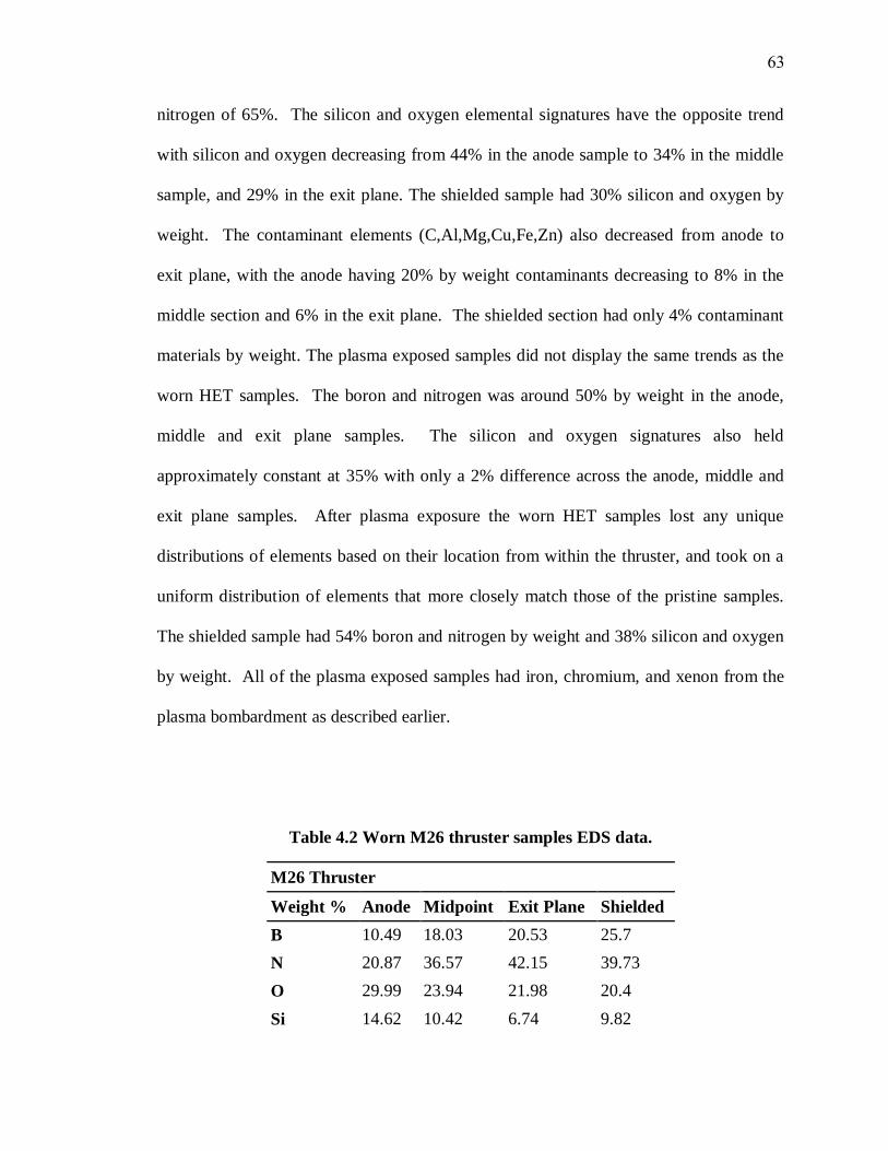
63
nitrogen of 65%. The silicon and oxygen elemental signatures have the opposite trend
with silicon and oxygen decreasing from 44% in the anode sample to 34% in the middle
sample, and 29% in the exit plane. The shielded sample had 30% silicon and oxygen by
weight. The contaminant elements (C,Al,Mg,Cu,Fe,Zn) also decreased from anode to
exit plane, with the anode having 20% by weight contaminants decreasing to 8% in the
middle section and 6% in the exit plane. The shielded section had only 4% contaminant
materials by weight. The plasma exposed samples did not display the same trends as the
worn HET samples. The boron and nitrogen was around 50% by weight in the anode,
middle and exit plane samples. The silicon and oxygen signatures also held
approximately constant at 35% with only a 2% difference across the anode, middle and
exit plane samples. After plasma exposure the worn HET samples lost any unique
distributions of elements based on their location from within the thruster, and took on a
uniform distribution of elements that more closely match those of the pristine samples.
The shielded sample had 54% boron and nitrogen by weight and 38% silicon and oxygen
by weight. All of the plasma exposed samples had iron, chromium, and xenon from the
plasma bombardment as described earlier.
Table 4.2 Worn M26 thruster samples EDS data.
M26 Thruster
Weight % Anode Midpoint Exit Plane Shielded
B 10.49 18.03 20.53 25.7
N 20.87 36.57 42.15 39.73
O 29.99 23.94 21.98 20.4
Si 14.62 10.42 6.74 9.82
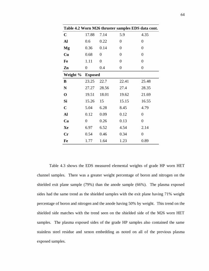
64
Table 4.2 Worn M26 thruster samples EDS data cont.
C 17.88 7.14 5.9 4.35
Al 0.6 0.22 0 0
Mg 0.36 0.14 0 0
Cu 0.68 0 0 0
Fe 1.11 0 0 0
Zn 0 0.4 0 0
Weight % Exposed
B 23.25 22.7 22.41 25.48
N 27.27 28.56 27.4 28.35
O 19.51 18.01 19.62 21.69
Si 15.26 15 15.15 16.55
C 5.04 6.28 8.45 4.79
Al 0.12 0.09 0.12 0
Ca 0 0.26 0.13 0
Xe 6.97 6.52 4.54 2.14
Cr 0.54 0.46 0.34 0
Fe 1.77 1.64 1.23 0.89
Table 4.3 shows the EDS measured elemental weights of grade HP worn HET
channel samples. There was a greater weight percentage of boron and nitrogen on the
shielded exit plane sample (79%) than the anode sample (66%). The plasma exposed
sides had the same trend as the shielded samples with the exit plane having 71% weight
percentage of boron and nitrogen and the anode having 50% by weight. This trend on the
shielded side matches with the trend seen on the shielded side of the M26 worn HET
samples. The plasma exposed sides of the grade HP samples also contained the same
stainless steel residue and xenon embedding as noted on all of the previous plasma
exposed samples.
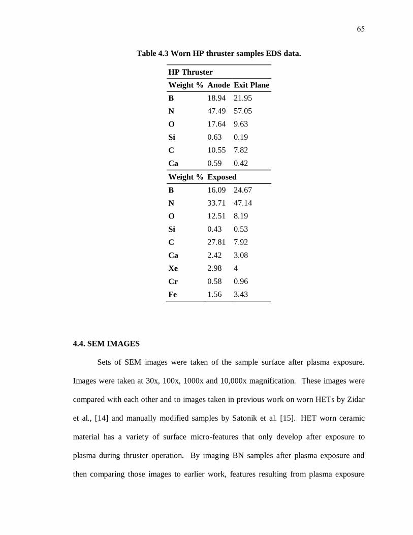
65
Table 4.3 Worn HP thruster samples EDS data.
HP Thruster
Weight % Anode Exit Plane
B 18.94 21.95
N 47.49 57.05
O 17.64 9.63
Si 0.63 0.19
C 10.55 7.82
Ca 0.59 0.42
Weight % Exposed
B 16.09 24.67
N 33.71 47.14
O 12.51 8.19
Si 0.43 0.53
C 27.81 7.92
Ca 2.42 3.08
Xe 2.98 4
Cr 0.58 0.96
Fe 1.56 3.43
4.4. SEM IMAGES
Sets of SEM images were taken of the sample surface after plasma exposure.
Images were taken at 30x, 100x, 1000x and 10,000x magnification. These images were
compared with each other and to images taken in previous work on worn HETs by Zidar
et al., [14] and manually modified samples by Satonik et al. [15].
HET worn ceramic
material has a variety of surface micro-features that only develop after exposure to
plasma during thruster operation. By imaging BN samples after plasma exposure and
then comparing those images to earlier work, features resulting from plasma exposure
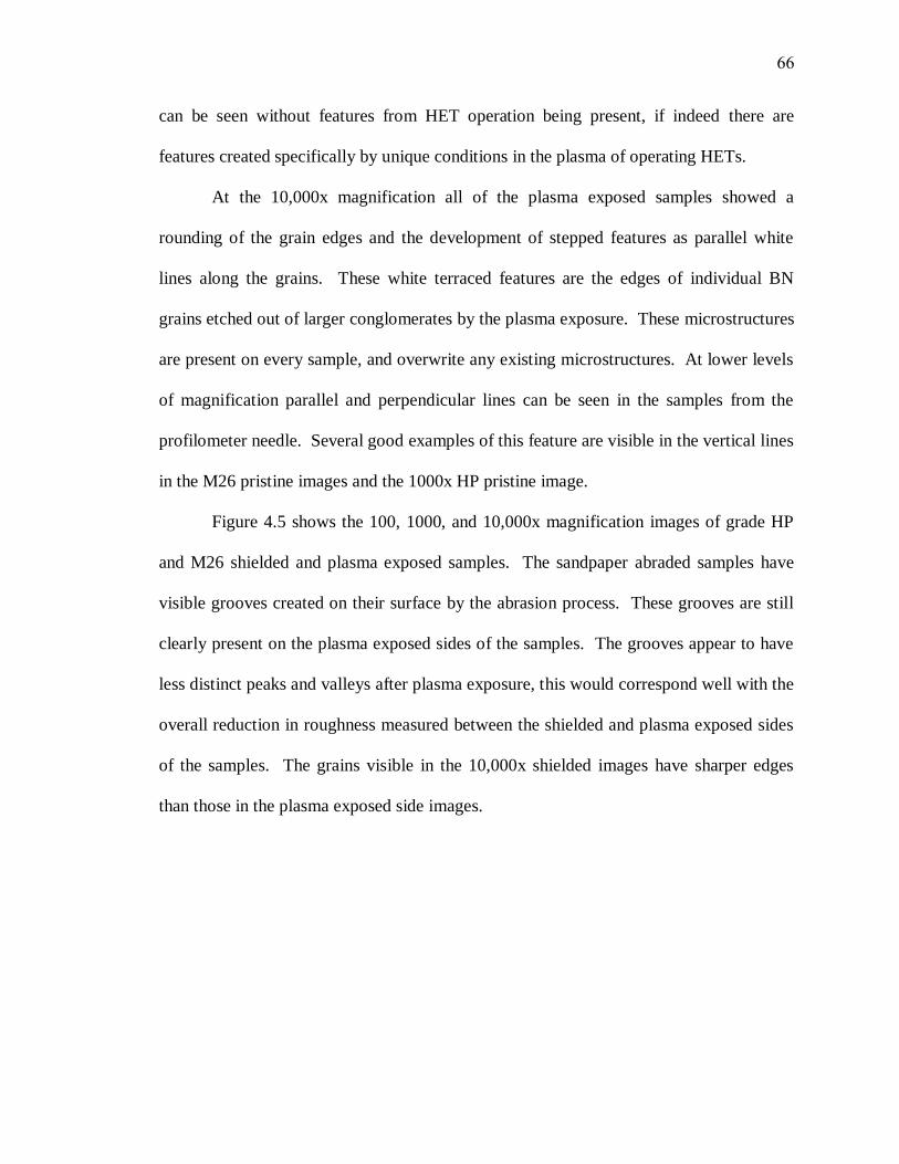
66
can be seen without features from HET operation being present, if indeed there are
features created specifically by unique conditions in the plasma of operating HETs.
At the 10,000x magnification all of the plasma exposed samples showed a
rounding of the grain edges and the development of stepped features as parallel white
lines along the grains. These white terraced features are the edges of individual BN
grains etched out of larger conglomerates by the plasma exposure. These microstructures
are present on every sample, and overwrite any existing microstructures. At lower levels
of magnification parallel and perpendicular lines can be seen in the samples from the
profilometer needle. Several good examples of this feature are visible in the vertical lines
in the M26 pristine images and the 1000x HP pristine image.
Figure 4.5 shows the 100, 1000, and 10,000x magnification images of grade HP
and M26 shielded and plasma exposed samples. The sandpaper abraded samples have
visible grooves created on their surface by the abrasion process. These grooves are still
clearly present on the plasma exposed sides of the samples. The grooves appear to have
less distinct peaks and valleys after plasma exposure, this would correspond well with the
overall reduction in roughness measured between the shielded and plasma exposed sides
of the samples. The grains visible in the 10,000x shielded images have sharper edges
than those in the plasma exposed side images.
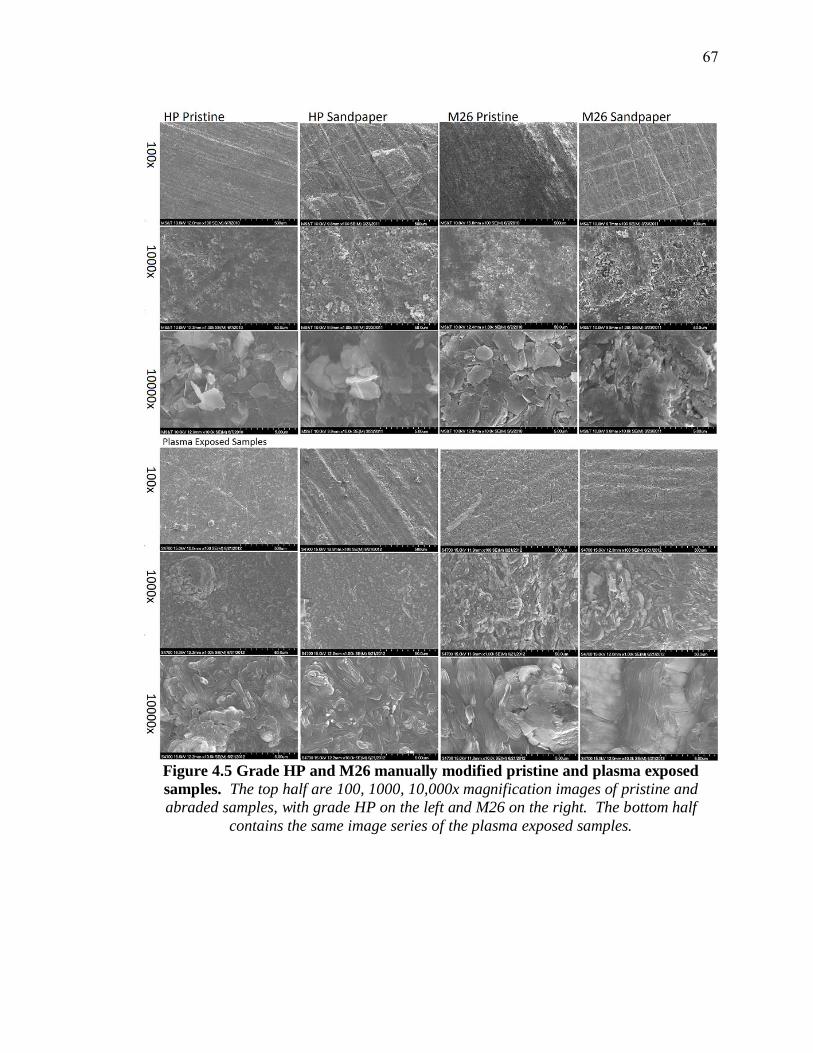
67
Figure 4.5 Grade HP and M26 manually modified pristine and plasma exposed
samples. The top half are 100, 1000, 10,000x magnification images of pristine and
abraded samples, with grade HP on the left and M26 on the right. The bottom half
contains the same image series of the plasma exposed samples.
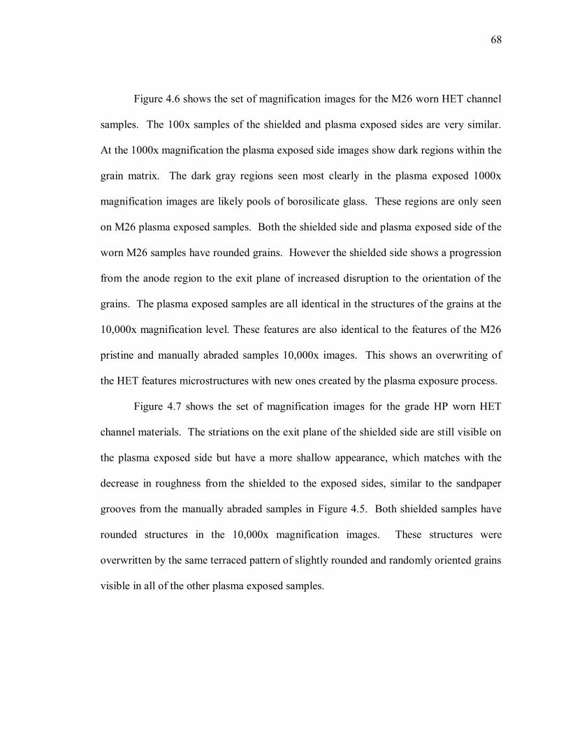
68
Figure 4.6 shows the set of magnification images for the M26 worn HET channel
samples. The 100x samples of the shielded and plasma exposed sides are very similar.
At the 1000x magnification the plasma exposed side images show dark regions within the
grain matrix. The dark gray regions seen most clearly in the plasma exposed 1000x
magnification images are likely pools of borosilicate glass. These regions are only seen
on M26 plasma exposed samples. Both the shielded side and plasma exposed side of the
worn M26 samples have rounded grains. However the shielded side shows a progression
from the anode region to the exit plane of increased disruption to the orientation of the
grains. The plasma exposed samples are all identical in the structures of the grains at the
10,000x magnification level. These features are also identical to the features of the M26
pristine and manually abraded samples 10,000x images. This shows an overwriting of
the HET features microstructures with new ones created by the plasma exposure process.
Figure 4.7 shows the set of magnification images for the grade HP worn HET
channel materials. The striations on the exit plane of the shielded side are still visible on
the plasma exposed side but have a more shallow appearance, which matches with the
decrease in roughness from the shielded to the exposed sides, similar to the sandpaper
grooves from the manually abraded samples in Figure 4.5. Both shielded samples have
rounded structures in the 10,000x magnification images. These structures were
overwritten by the same terraced pattern of slightly rounded and randomly oriented grains
visible in all of the other plasma exposed samples.
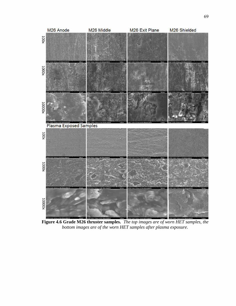
69
Figure 4.6 Grade M26 thruster samples. The top images are of worn HET samples, the
bottom images are of the worn HET samples after plasma exposure.

70
Figure 4.7 Grade HP thruster samples. The top half
has 100, 1000, and 10000x images of the worn samples,
the bottom half has the same magnification images of
the plasma exposed samples.
71
5. DISCUSSION
The results of the plasma exposure tests showed that the BN ceramic was affected
in a variety of ways by the plasma source. The sputter rate was dependent on material
grades and surface preparation. Unique microstructures were also created by the plasma
exposure. However these microstructures only shared a few similarities with those seen
on worn HET samples.
5.1. MANUAL MODIFICATION LEADS TO INCREASED EROSION
Manual modification of samples prior to plasma exposure resulted in an increase
in the amount of erosion of the sample material. Sputter rates of materials can be
affected by a variety of factors including angle of incidence of the bombarding particles,
defect presence and density, and in the case of multiple component materials, the separate
components can have separate sputter rates [34-36]. In all of the ceramic grades of BN,
boron nitride is theorized to be the constituent most resilient to sputter erosion due to the
strong covalent bond between the boron and nitrogen atoms [7,21,22,37,38]. Further, all
of the BN samples have a surface roughness much greater than the grain size. This
allows for the surface to be treated as a series of flat plates at random angles with respect
to the direction of ion bombardment from the magnetron plasma [38]. This greatly
decreases the effect of incidence angle on ion bombardment sputtering rate of the
samples. The process of modifying the ceramic through tooling or sandpaper creates a
layer of cracked material on the top of the sample surface [15]. Under plasma exposure

72
and ion bombardment, these cracks can be expanded [36]. As the cracks expand and
intersect with one another large sections of material can become separated allowing for
platelet removal via sputtering. Existing cracks and defects from manual modification
allow for those modified samples to erode faster than their less-damaged counterparts.
Grade M26 showed the greatest increase in erosion following manual abrasion
modification, with a 51% increase. Of interest is the disconnect between the roughness
increase of samples due to sandpaper modification and the resulting erosion increases.
Pristine grade HP had a larger roughness increase from the pristine to the abraded sample
compared to grade M26. With a similar boron nitride used between the grades, and the
method of abrasion held constant across all of the samples, the cause of the differences in
roughness lies in the binding agent variations among the samples. Grade HP uses
calcium borate as a binding agent, but at a low percentage, with 90% of the ceramic being
composed of boron nitride, as compared to only 60% of grade M26 being composed of
boron nitride. As a result when manual damage is done to the surface of the ceramic,
more material is completely removed leaving a thinner section of damage that then
erodes more quickly under ion bombardment. With M26, less material is lost during the
initial manual modification, which results in less roughness, but there are more residual
cracks and defects created in the material allowing the sputter process to accelerate the
erosion of the sample.
5.2. CHEMICAL COMPOSITION CHANGES
Previous work done on the surface elemental composition of HETs has shown a
trend of increasing BN ratios with proximity to the exit plane of the thruster [14]. The
73
worn thruster channel samples that were exposed to plasma in the magnetron did not
show this trend and returned to a ratio of BN to binder close to that of the listed pristine
values. This suggests that the increase in the BN to binder ratio observed in worn HETs
is a surface feature, which does not affect the underlying bulk material. It also suggests
that the BN to binder ratio changes are specific to conditions in the HET. Whether the
change in BN to binder ratios is a result of sputter erosion, or a combination of erosion
and redepositon of sputter materials requires further study.
Xenon gas was detected on all of the sputtered samples. Based on the values of
xenon in the EDS and XPS results, the majority of the xenon gas is at least 10 nm below
the surface of the samples. Ion implantation is known to affect the material properties of
the substrate into which the ions are imbedded. The exact changes to the material can be
very complex and depend on many factors including, the energy and size of the imbedded
ion, the crystal structure and chemical composition of the substrate, and annealing effects
from heating during and after ion bombardment. While no analysis of the material
properties of the BN samples were carried out post plasma exposure, a reasonable
hypothesis given the size of the xenon atom compared to the BN crystal structure is that
the BN is weakened due to the stresses placed on the crystal lattice from the inclusion of
the xenon atoms [34-37]. Since xenon gas was not present in the work done by Zidar et
al., [14] the xenon may diffuse out over time. However Khartov measured trapped xenon
in worn HET samples, but with the plasma exposed samples being coated with stainless
steel during plasma exposure the xenon deposited in the ceramic may have been better
contained with many of its out-gassing routes blocked by deposited stainless steel [33].
74
5.3. UNIFORMITY OF MICROSTRUCTURES
Of all of the microstructures observed on worn HETs and manually modified
samples, only the largest features are recognizable after plasma exposure, such as grooves
from low grit sandpaper or thruster exit plane striations.
In place of the variety of microstructures, one dominant structure is observed after
exposure: rounded and step cut grains. Previous work done by Garnier et al., [21] and
Peterson et al., [24] also showed rounding of the otherwise sharp angled hexagonal BN
grains. These results match well with established sputter theory suggesting that
sputtering is easier at coroners and around defect locations [36]. In contrast, work by
Yalin et al., did not show rounded or step cut grains [38]. Their experiment used a
directional ion beam, not a plasma source. While individual grains in their experiment
did see some softening of the edges, the larger rounded structures did not appear.
The step cuts seen as parallel white lines on the 10,000x magnification SEM
images are caused by the anisotropic material properties of hexagonal BN. While each
layer is held together internally with strong covalent bonds, the separate layers are held
together only by Van der Waals forces [29]. This allows for an ion entering at an angle
close to parallel between layers in a grain to penetrate deeper and cause much more
damage the an ion hitting perpendicular to the face of the grain. This effect would be
most pronounced between the flat faces of the platelets that compose the individual
grains. Thus each white line seen in the images is part of the edge of a grain ceramic
material,
Examination of the density of these step cuts and grain orientation in the 10,000x
SEM images shows far more steps on grains oriented with their sides facing upward as
compared to grains lying flat. Each grain individually can have a different erosion rate

75
based on its orientation to the sputter ions, but given a surface roughness larger than the
grain size, the random orientation of the grains across the entire surface will result in the
sample having less dependence on orientation to determine sputter erosion rate [34-36].
The dark regions visible in the M26 plasma exposed samples, shown in spectrum
2 of Figure 5.1, are areas of pooled borosilicate glass. Table 5.1 shows only Si and O
signatures in the pool regions. These pools are evident only in BN samples using SiO2 as
a binding agent, and only appear after plasma exposure in the magnetron plasma source.
There is no evidence of these pools in samples from worn HETs that have not been
further plasma exposed in the magnetron. The preparation of the samples prior to plasma
exposure does not affect the creation of these features, as the pools are on the pristine,
worn HET, and abraded samples. These pools could be a result of localized heating on
the sample allowing the SiO2 to flow and collect. If these pools are leaching SiO2 out of
the ceramic the grains of boron nitride would be more easily removed via sputtering since
there would be less binding agent holding them in place.
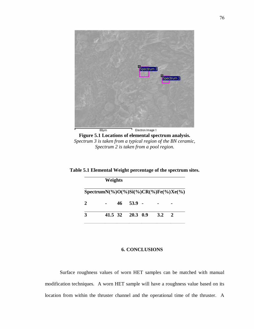
76
Table 5.1 Elemental Weight percentage of the spectrum sites.
6. CONCLUSIONS
Surface roughness values of worn HET samples can be matched with manual
modification techniques. A worn HET sample will have a roughness value based on its
location from within the thruster channel and the operational time of the thruster. A
Weights
Spectrum N(%) O(%) Si(%) CR(%) Fe(%) Xe(%)
2 - 46 53.9 - - -
3 41.5 32 20.3 0.9 3.2 2
Figure 5.1 Locations of elemental spectrum analysis.
Spectrum 3 is taken from a typical region of the BN ceramic,
Spectrum 2 is taken from a pool region.
77
pristine sample of BN can be manually modified to have a roughness value to match that
of the worn HET sample. However the method of modification used on a BN sample can
have a significant effect on its erosion rate under plasma exposure, with abraded samples
having more surface damage allowing for faster erosion under plasma exposure.
With the exception of xenon, impurities deposited onto the surface of BN samples
are only present in the top most layer of the sample. The stainless steel layer on the
surface of the plasma exposed samples had the strongest signature in the top 10 nm of the
sample. The signature from the xenon gas was stronger in the deeper scanning EDS
measurements implying more xenon is deposited deeper in the sample, at least 10 nm and
possibly up to 340 nm as Khartov measured. Some of the worn HET samples contained
ratios of BN to binding agent significantly different from the factory listed ratios for the
ceramic in their surface layers which is attributed to plasma conditions in the thruster.
These ratios were completely overwritten after plasma exposure, and returned to a ratio
resembling the listed value.
Some surface features on worn HET channel material are a result of the specific
plasma conditions present in the HET. Exposure to plasma in the magnetron causes
microstructure changes that are not seen under pure ion beam erosion. Specifically the
rounding of the grains and knobby structures seen in worn HET samples and plasma
exposed samples were not seen in ion beam tests done by Yalin [38]. The
microstructures created by plasma exposure, while more similar to some features seen in
worn HETs (the rounding of individual grains) still lack some of the major features noted
in worn HETs, specifically the exit plane striations. In order to replicate these features
samples must be placed in a HET plasma environment.
78
The binding agent used in the various grades of BN plays a significant part in the
mechanical properties of the BN. Grade M26 was damaged less than grade HP under
manual abrasion. However trends in macroscopic mechanical proprieties are not
necessarily held at the atomic level under sputter erosion. In theory the binding agent of
the BN ceramic should be the fastest material to be lost under sputter erosion, which is
validated based on the EDS measurements of Si and O between the shielded and plasma
exposed sides of the M26 samples. This suggests a compromise is necessary between
mechanical properties and sputtering resistance for the binding agents used in BN
ceramics.
79
REFERENCES
[1] Fife, J. M., Gibbons, M. R., Hargus, W. A., VanGilder, D. B. and Kirtley, D. B.,
“3-D Computation of Surface Sputtering and Redeposition Due to Hall Thruster
Plumes,” International Electric Propulsion Conference, IEPC, 2003.
[2] Hofer, R. R., Mikellides, I. G., Katz, I. and Goebel, D. M., “Wall Sheath and
Electron Mobility Modeling in Hybrid-PIC Hall Thruster Simulations,” 43rd
AIAA/ASME/SAE/ASEE Joint Propulsion Conference and Exhibit, AIAA, 2007.
[3] Ivanov, A. A., Ivanov Jr., A. A. and Bacal, M., “Effect of plasma-wall
recombination on the conductivity of Hall thrusters,” Plasma Physics and
Controlled Fusion, Vol. 44, No. 7, 2002, pp. 1463-1470.
[4] Sommier, E., Allis, M. K., Gascon, N. and Cappelli, M. A., “Wall Erosion in 2D
Hall Thruster Simulations,” 42nd
AIAA/ASME/SAE/ASEE Joint Propulsion
Conference and Exhibit, AIAA, 2006.
[5] Sullivan, K., Fox, J., Martinez-Sanchez, M. and Batischev, O., “Kinetic Study of
Wall Effect in SPT Hall Thrusters,” 40th
AIAA/ASME/SAE/ASEE Joint Propulsion
Conference and Exhibit, AIAA, 2004.
[6] Locke, S., Shumlak, U. and Fife, J. M., “Effect of a Channel Wall Discontinuity
in an SPT-Type Hall Thruster,” 37th AIAA/ASME/SAE/ASEE Joint Propulsion
Conference, AIAA, 2001.
[7] Meng C., Guido R., Andreas N., Karl-L.B., and Achim L., “Simulation of Boron
Nitride Sputtering Process and Its Comparison with Experimental Data,” IEEE
Transactions on Plasma Science, VOL. 26, NO. 6, 1998, pages 1713-1717.
[8] Daren Yu, Yuquan Li and Shenhua Song, “Ion sputtering erosion of channel wall
corners in Hall thrusters ,” 2006 J. Phys. D: Appl. Phys. 39: 2205.
[9] Raitses, Y., Staack, D., Keidar, M. and Fisch, N. J., “Electron-wall interaction in
Hall thrusters,” Physics of Plasmas, Vol. 12. No. 5, 2005: 057104.
[10] Dunaevsky, A., Raitses, Y. and Fisch, N. J., “Secondary electron emissions from
dielectric materials of a Hall thruster with segmented electrodes,” Physics of
Plasmas, Vol. 10, No. 6, 2003, pp. 2574-2577.
[11] Raitses, Y., Smirnov, A., Staack, D. and Fisch, N. J., “Measurements of
secondary electron emission effects in the Hall thruster discharge,” Physics of
Plasmas, Vol. 13, No. 1, 2006: 014502.
[12] Gascon, N., Dudeck, M. and Barral, S., “Wall material effects in stationary
plasma thrusters. I. Parametric studies of an SPT-100,” Physics of Plasmas, Vol.
10, No. 10, 2003, pp. 4123-4136.

80
[13] Yong, Y. C., Thong, J. T. L. and Phang, J. C. H., “Determination of secondary
electron yield from insulators due to a low-kV electron beam,” Journal of Applied
Physics, Vol. 84, No. 8, 1998, pp. 4543-4548.
[14] Zidar, D. G., Rovey, J. L., “Hall-effect Thruster Channel Surface Properties
Investigation,” Journal of Propulsion and Power, vol. 28 No. 2 , 2012, pp. 334-
343.
[15] Satonik, A.J. and Rovey, J.L., “Modification of Boron Nitride Ceramic to
Replicate Hall-effect Thruster Surface Wear,” AIAA-2012-0198, 50th Aerospace
Sciences Meeting, Nashville, TN., Jan 9-12, 2012.
[16] Mason, L. S., Jankovsky, R. S. and Manzella, D. H., “1000 Hours of Testing on a
10 Kilowatt Hall Effect Thruster,” 37th
AIAA /ASME/SAE/ASEE Joint Propulsion
Conference and Exhibit, AIAA, 2001.
[17] de Grys, K., Mathers, A., Welander, B. and Khayms, V., “Demonstration of
10,400 Hours of Operation on a 4.5 kW Qualification Model Hall Thruster,” 46th
AIAA/ASME/SAE/ASEE Joint Propulsion Conference &Exhibit, AIAA, 2010.
[18] Peterson, P. Y. and Manzella, D. H., “Investigation of the Erosion Characteristics
of a Laboratory Hall Thruster,” 39th AIAA/ASME/SAE/ASEE Joint Propulsion
Conference and Exhibit, AIAA, 2003.
[19] Morozov, I A., “The Conceptual Development of Stationary Plasma Thrusters,”
Plasma Physics Reports, Vol. 29, No. 3, 2003, pp. 235-250. (Translated from
Russian. Originally published in Fizika Plazmy, Vol 29, No, 3,pp. 261-276.)
[20] Choueiri, E. Y., “Fundamental Difference Between the Two Hall Thruster
Variants,” Physics of Plasmas, Vol. 8, No. l, 2001, pp. 5025-5033.
[21] Garnier, Y., Viel, V., Roussel, J. F. and Bernard, J., “ Low-energy xenon ion
sputtering of ceramics investigated for stationary plasma thrusters,” Journal of
Vacuum Science and Technology, Vol. 17, No. 6, 1999, pp. 3246-3254.
[22] Garnier, Y., Viel, V., Roussel, J. F., Pagnon, D., Mange, L. and Touzeau, M.,
“Investigation of Xenon Ion Sputtering of One Ceramic Material Used in SPT
Discharge Chamber,” 26th International Electric Propulsion Conference, IEPC,
1999, pp. 512-517.
[23] Shon C.H., Lee J.K., “Modeling of magnetron sputtering plasmas,” Applied
Surface Sciences, 192.1 (2002) pages 258-269.
[24] Peterson, P. Y., Jacobson, D. T., Manzella, D. H. and John, J. W., “The
Performance and Wear Characterization of a High-Power High-Isp NASA Hall
Thruster,” 41st AIAA /ASME/SAE/ASEE Joint Propulsion Conference and Exhibit,
2005.
[25] B. Rubin, J. L. Topper, and A. P. Yalin, “Total and Differential Sputter Yields of
Boron Nitride Measured by Quartz Crystal Microbalance,” 31st International
Electric Propulsion Conference, 2009.

81
[26] Combat® Solid Boron Nitride Composite Grade HP. [Online] February 2006.
[Cited: September 9, 2010.] http://www.bn.saint-
gobain.com/uploadedFiles/SGbn/Documents/Solids/Solid-Combat-BN-
GradeHP.pdf.
[27] Combat® Solid Boron Nitride Composite Grades M and M26. [Online] June
2003. [Cited: September 9, 2010.] http://www.bn.saint-
gobain.com/uploadedFiles/SGbn/Documents/Solids/Solid-Combat-GradesM-
M26.pdf.
[28] Sloan Technology Corporation, Dektak IIA Manual, Sloan Technology
Corporation, Santa Barbara, CA, 1984, p. i.
[29] Goldstein, J. I., Newbury, D. E., Echlin, P., Joy, D. C., Romig, Jr., A. D., Lyman,
C. E., Fiori, C. and Lifshin, E., Scanning Electron Microscopy and X-ray
Microanalysis. 2nd
edition, Plenum Press, New York. 1992. pp. 21-25, 292-311.
[30] P. Beiss, G. Leichtfried et al. (2002). “Properties of diamond and cubic boron
nitride”. Landolt-Börnstein– Group VIII Advanced Materials and Technologies:
Powder Metallurgy Data. Refractory, Hard and Intermetallic Materials. 2A2.
Berlin: Springer. pp. 118– 139.
[31] P. Sigmund, “Theory of sputtering I: sputtering yield of amorphous and
polycrystalline targets,” Phys. Rev. 184, 1969, pages 383-416.
[32] R. Santos, Y. Raitses, “Transitional regime in the start-up process of conventional
Hall thrusters,” 32th International Electric Propulsion Conference (Wiesbaden
Germany, 2011).
[33] Khartov, S. A. Nadiradze and O. Duchemin, “SPT Ceramic Isolator Surfaced
Layer Composition Change with Lifetime.” IEPC-2003-059, 28th
International
Electric Propulsion Conference, Toulouse, France, March 2003.
[34] M.V. Ramana Murty, “Sputtering: the material erosion tool,” Surface Science,
500, (2002) pages 523–544.
[35] P. Sigmund, “Theory of sputtering I: sputtering yield of amorphous and
polycrystalline targets,” Phys. Rev. 184, 1969, pages 383-416.
[36] Stoller, R. E., & Guiriec, S. G. (2004). “Secondary factors influencing cascade
damage formation,” Journal of nuclear materials, 329, pages 1238-1242.
[37] Doerner, R. P., Whyte, D. G., & Goebel, D. M. (2003). “Sputtering yield
measurements during low energy xenon plasma bombardment” Journal of
Applied Physics, 93(9), 5816-5823.
[38] Yalin, A.P., Rubin, B., Domingue, S.R., Glueckert, Z., and Williams, J.D.,
“Differential Sputter Yields of Boron Nitride, Quartz, and Kapton Due to Low
Energy Xe+ Bombardment”, 43rd AIAA/ASME/SAE/ASEE Joint Propulsion
Conference, AIAA paper 2007: 5314.
[39] J. D. Williams, M. M. Gardner, M. Johnson, and P. J. Wilbur, “Xenon sputter
yield measurements for ion thruster materials,” 28th International Electric
Propulsion Conference (Centre National D'Etudes Spatiales, 2003), paper: 0130.
82
SECTION
2. CONCLUSION
Sandpaper and abrasive blaster modification methods have both shown the ability
to match the numerical roughness values seen at any location in a worn HET as measured
by Zidar and Rovey. However the structures responsible for roughness values in worn
HET's look substantially different from the structures created by both methods of
abrasion. The recommended method to match a pristine sample’s surface roughness value
to a worn sample’s roughness value would be to choose a grit size that produces a
maximum roughness after prolonged abrasion which matches the worn roughness value.
Vacuum heating has shown an ability to modify the microstructures and chemical
composition of the samples. However other microstructures seen in the worn HET have
yet to be reproduced. Heating can be used to modify the amount of binding agent in the
BN samples. With a wider range of heated data points it may be possible to replicate
specific ratios of boron nitride to binding agent seen at different locations in the worn
HET.
With the exception of xenon, impurities deposited onto the surface of BN samples
are only present in the top most layer of the sample. This result holds for both the
magnetron sputter experiments, and for studies on worn thrusters previously. The
stainless steel layer on the surface of the plasma exposed samples in the magnetron
83
sputter experiment had the strongest signature in the top 10 nm of the sample. The
signature from the xenon gas was stronger in the deeper scanning EDS measurements
implying more xenon is deposited deeper in the sample, at least 10 nm and possibly up to
340nm. Some of the worn HET samples contained ratios of BN to binding agent
significantly different from the factory listed ratios for the ceramic in their surface layers
which is attributed to plasma conditions in the thruster. These ratios were completely
overwritten after plasma exposure, and returned to a ratio resembling the listed value.
Some surface features on worn HET channel material are a result of the specific
plasma conditions present in the HET. Exposure to plasma in the magnetron causes
microstructure changes that are not seen under pure ion beam erosion. Specifically the
rounding of the grains and knobby structures seen in worn HET samples and plasma
exposed samples were not seen in ion beam tests done by Yalin. The microstructures
created by plasma exposure, while similar to some features seen in worn HETs (the
rounding of individual grains) still lack some of the major features noted in worn HETs,
specifically the exit plane striations. In order to replicate these features samples must be
placed in a HET plasma environment.
The binding agent used in the various grades of BN plays a significant part in the
mechanical properties of the BN. Grade M26 was damaged less than grade HP under
manual abrasion. However trends in macroscopic mechanical proprieties are not
necessarily held at the atomic level under sputter erosion. In theory the binding agent of
the BN ceramic should be the fastest material to be lost under sputter erosion, which is
validated based on the EDS measurements of Si and O between the shielded and plasma
exposed sides of the M26 samples. This suggests a compromise is necessary between
mechanical properties and sputtering resistance for the binding agents used in BN
ceramics.

APPENDIX A.
RESULTS AND DISCUSSION OF PLASMA EXPOSED GRADES A AND M
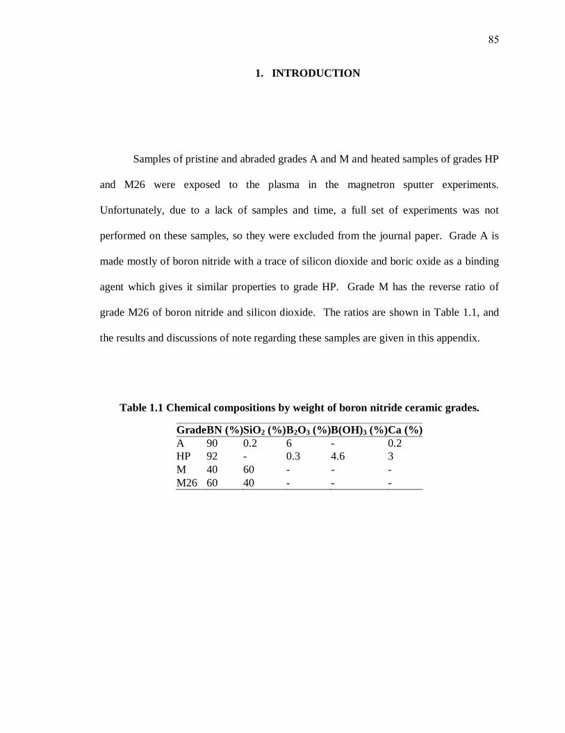
85
1. INTRODUCTION
Samples of pristine and abraded grades A and M and heated samples of grades HP
and M26 were exposed to the plasma in the magnetron sputter experiments.
Unfortunately, due to a lack of samples and time, a full set of experiments was not
performed on these samples, so they were excluded from the journal paper. Grade A is
made mostly of boron nitride with a trace of silicon dioxide and boric oxide as a binding
agent which gives it similar properties to grade HP. Grade M has the reverse ratio of
grade M26 of boron nitride and silicon dioxide. The ratios are shown in Table 1.1, and
the results and discussions of note regarding these samples are given in this appendix.
Table 1.1 Chemical compositions by weight of boron nitride ceramic grades.
Grade BN (%) SiO2 (%) B2O3 (%) B(OH)3 (%) Ca (%)
A 90 0.2 6 - 0.2
HP 92 - 0.3 4.6 3
M 40 60 - - -
M26 60 40 - - -
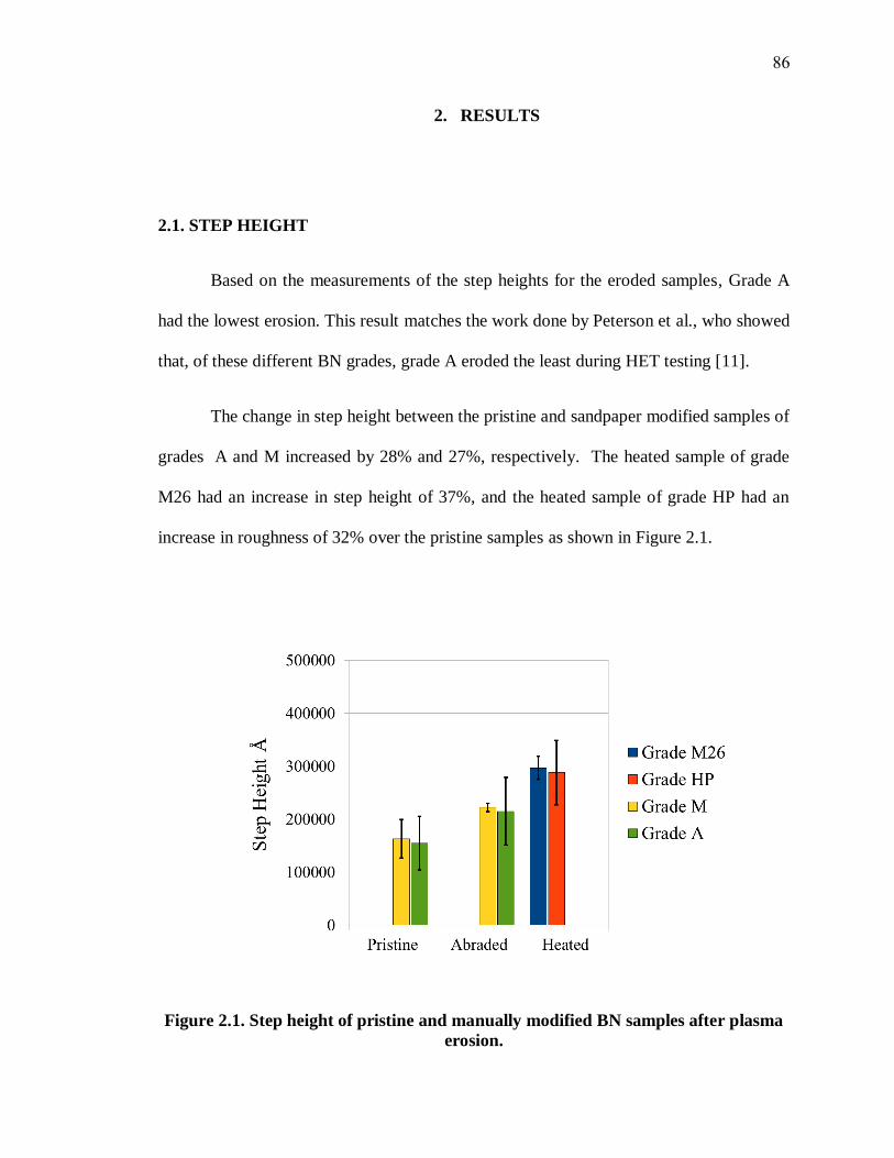
86
2. RESULTS
2.1. STEP HEIGHT
Based on the measurements of the step heights for the eroded samples, Grade A
had the lowest erosion. This result matches the work done by Peterson et al., who showed
that, of these different BN grades, grade A eroded the least during HET testing [11].
The change in step height between the pristine and sandpaper modified samples of
grades A and M increased by 28% and 27%, respectively. The heated sample of grade
M26 had an increase in step height of 37%, and the heated sample of grade HP had an
increase in roughness of 32% over the pristine samples as shown in Figure 2.1.
Figure 2.1. Step height of pristine and manually modified BN samples after plasma
erosion.
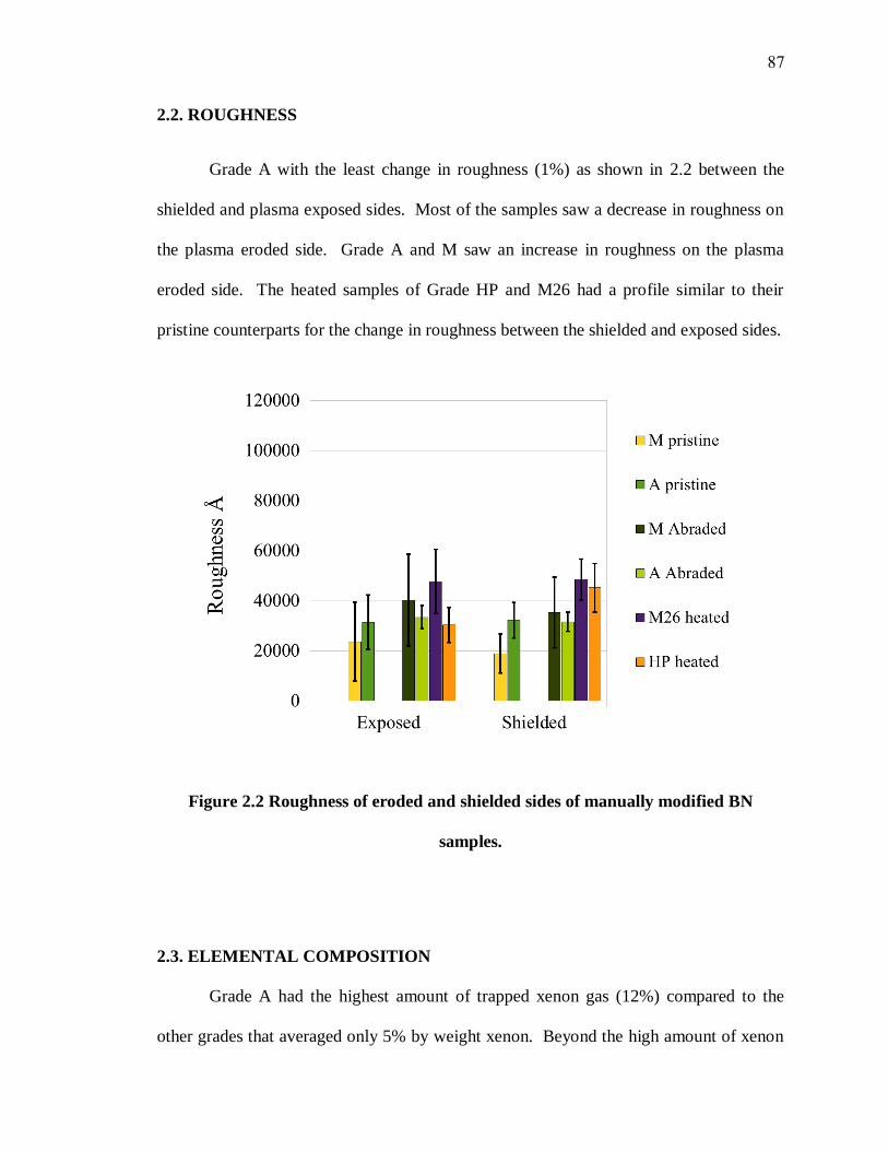
87
2.2. ROUGHNESS
Grade A with the least change in roughness (1%) as shown in 2.2 between the
shielded and plasma exposed sides. Most of the samples saw a decrease in roughness on
the plasma eroded side. Grade A and M saw an increase in roughness on the plasma
eroded side. The heated samples of Grade HP and M26 had a profile similar to their
pristine counterparts for the change in roughness between the shielded and exposed sides.
Figure 2.2 Roughness of eroded and shielded sides of manually modified BN
samples.
2.3. ELEMENTAL COMPOSITION
Grade A had the highest amount of trapped xenon gas (12%) compared to the
other grades that averaged only 5% by weight xenon. Beyond the high amount of xenon
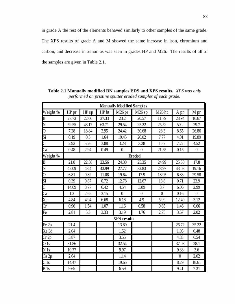
88
in grade A the rest of the elements behaved similarly to other samples of the same grade.
The XPS results of grade A and M showed the same increase in iron, chromium and
carbon, and decrease in xenon as was seen in grades HP and M26. The results of all of
the samples are given in Table 2.1.
Table 2.1 Manually modified BN samples EDS and XPS results. XPS was only
performed on pristine sputter eroded samples of each grade.
Manually Modified Samples
Weight % HP pr HP ht M26 pr M26 ht A pr M pr
B 27.73 22.06 27.33 23.2 20.57 11.79 28.94 16.67
N 59.55 48.17 63.71 29.54 25.22 25.52 50.2 29.7
O 7.28 18.84 2.95 24.42 30.68 28.3 8.65 26.86
Si 0.19 0.5 1.64 19.45 20.02 7.77 4.01 19.89
C 2.92 5.26 3.88 3.28 3.28 1.57 7.72 4.52
Ca 0.48 2.94 0.49 0 0 21.55 0.15 0
Weight % Eroded
B 21.8 22.58 23.56 24.38 25.35 24.99 25.58 17.8
N 47.09 43.4 43.99 27.77 32.83 28.97 43.03 19.16
O 6.81 9.82 11.08 19.64 17.9 18.95 6.83 29.58
Si 0.39 0.87 0.72 12.78 12.67 13.8 0.71 23.9
C 14.09 8.77 6.42 4.54 3.89 3.7 6.06 2.99
Ca 1.2 2.65 3.15 0 0 0 0.16 0
Xe 4.84 4.94 6.68 6.18 4.9 5.99 12.49 3.12
Cr 0.96 1.54 1.07 1.16 0.58 0.85 1.46 0.66
Fe 2.81 5.3 3.33 3.19 1.76 2.75 3.67 2.02
XPS results
Fe 2p 21.4 13.89 26.72 35.22
Xe 3d 2.04 1.52 1.05 0.48
Cr 2p 5.87 3.55 4.83 6.54
O 1s 31.86 32.54 37.03 28.1
N 1s 10.77 9.97 9.33 3.6
Ca 2p 2.64 1.14 0 2.02
C 1s 14.47 19.65 8.79 18.61
B 1s 9.65 6.59 9.41 2.31
HP sp M26 sp
89
2.4. SEM IMAGES
Grades A and M closely resemble their counterparts grades HP and M26 in the
features present in the SEM images. The exposed samples show more rounded grains
and terraced microstructures. Grade M shows darker pools of silicon dioxide as seen in
grade M26. The SEM images of grades A and M are shown in Figure 2.3.
Grade M which is composed of 40% BN and 60% SiO2 did not show the same
increase in wear the grade M26 did. In fact grade M compared well to grade A which
had the least amount of erosion due to sputtering. Grade M undoubtedly experiences
similar damage phenomena to grade M26 but given the increase in the amount of
predictions binder the residual cracking and defects left in the sample must not be enough
to allow the loss of larger chunks of material as seen in the images of grade M26.
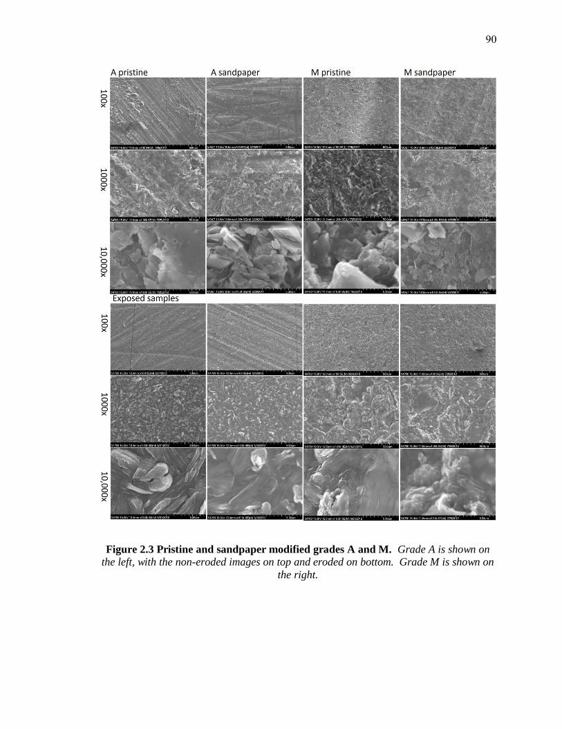
90
Figure 2.3 Pristine and sandpaper modified grades A and M. Grade A is shown on
the left, with the non-eroded images on top and eroded on bottom. Grade M is shown on
the right.
APPENDIX B.
BORON NITRIDE CERAMIC DATA SHEETS
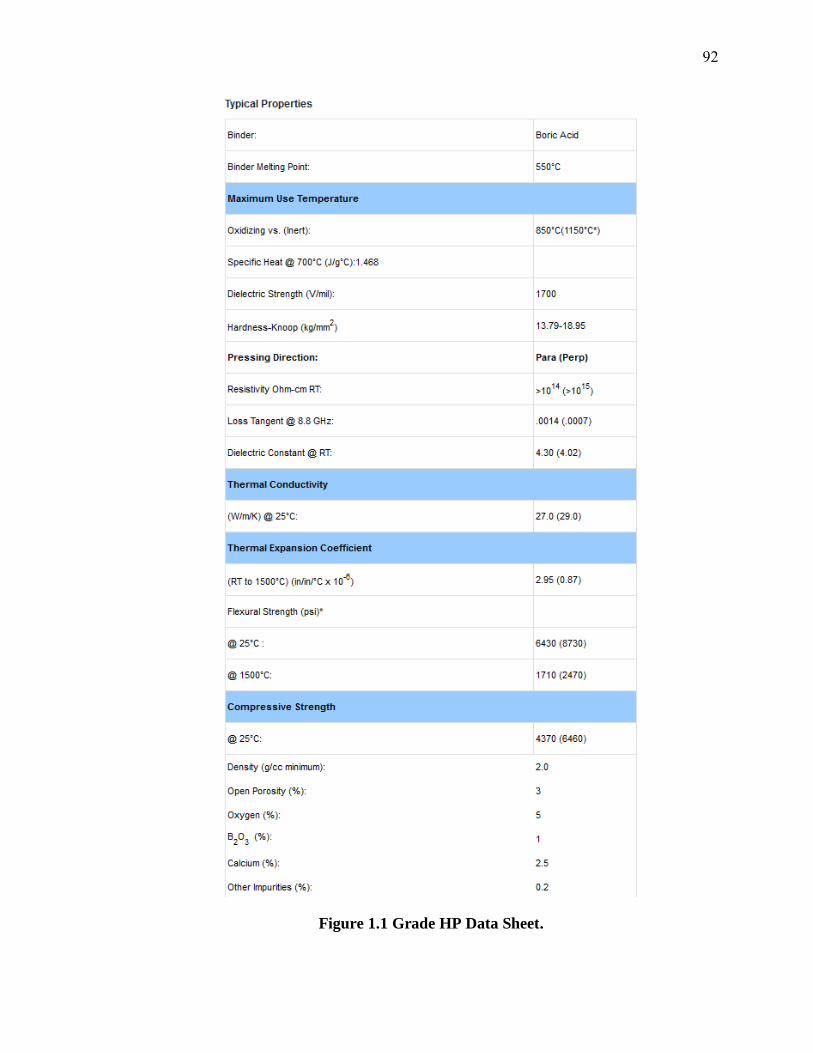
92
Figure 1.1 Grade HP Data Sheet.
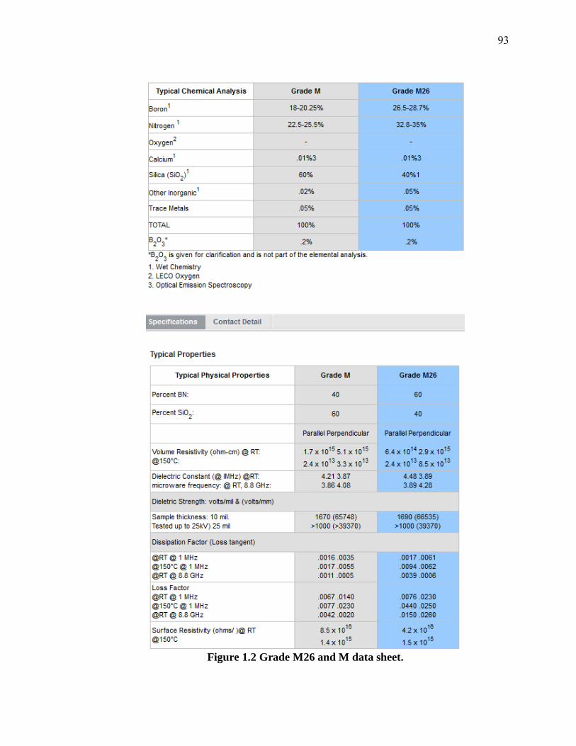
93
Figure 1.2 Grade M26 and M data sheet.

94
Figure 1.3 All BN grades data sheet.
95
VITA
Alexander John Satonik was born in Ohio in 1987. He spent his childhood
traveling the world with his family while his father served in the military. Then they
settled in Frankenmuth, Michigan where he attended high school. In 2005 he began a
program of study in aeronautical engineering at Western Michigan University. In 2010
he graduated with a Bachelor of Science in Aeronautical Engineering along with minors
in Mathematics and Astronomy. Following graduation, he moved to Rolla, Missouri to
further his education in The Missouri University of Science and Technology’s aerospace
engineering masters program. In 2013, he graduated with a Masters of Science in
Aerospace Engineering and a Certificate in Explosives Engineering.

Top Related