


Languages
Pages
Legal


Mahbube Hortamani21 December 2004
FHI-Berlin

• Introduction• Anistropic Magnetoresistance (AMR)• Giant Magnetoresistance (GMR)• Spin Valve• Magnetic Recording• Nonvolatile Memory• Spin transistor• Future Applications

Alloy and base metal targets (Ni/Fe, Co/Fe, Co/Cr/Pt, Pt/Mn, Ta, Cu, Au)
Two Types of MR Stripes
AMRAnisotropic Magneto-Resistance
4% Resistance ChangeThin Films Weakens effect
Introduced in 1992
GMRGiant Magneto-Resistance~200% Resistance Change
Thin films don't weaken effect as muchIntroduced in 1988

AMR The Anisotropic magnetoresistance measures the change in resistance for the current pass through a ferromagnetic media, when magnetization change from parallel to perpendicular to the
current.
δ− MnOCaLa xx1
Eckstein, Appl. Phy. Let. 69 1312 1996
T=160 K ; B= 0.5 T
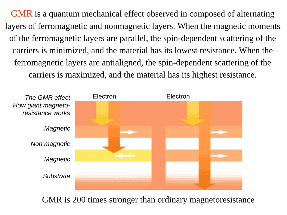
GMR is a quantum mechanical effect observed in composed of alternating layers of ferromagnetic and nonmagnetic layers. When the magnetic moments of the ferromagnetic layers are parallel, the spin-dependent scattering of the carriers is minimized, and the material has its lowest resistance. When the ferromagnetic layers are antialigned, the spin-dependent scattering of the
carriers is maximized, and the material has its highest resistance.
The GMR effect How giant magneto-
resistance works
Magnetic
Non magnetic
Magnetic
Substrate
Electron Electron
GMR is 200 times stronger than ordinary magnetoresistance
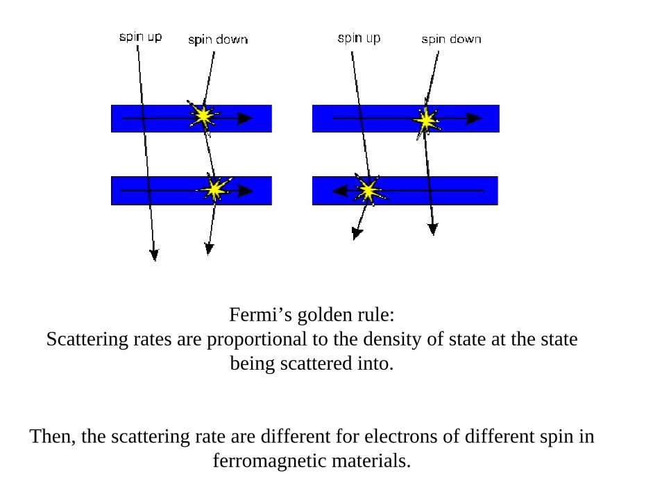
Fermi’s golden rule:Scattering rates are proportional to the density of state at the state
being scattered into.
Then, the scattering rate are different for electrons of different spin in ferromagnetic materials.

Spin-polarized transport will occur naturally in any material for which there is an imbalance of the spin populations at the Fermi level. It occurs in ferromagnetic metals because the density of states available to spin-up
and spin-down electrons is often nearly identical, but the states are shifted in energy with respect to each other.
↓↑
↓↑
+−
=nnnn
PPolarization defined as :Prinz 1995

FM SC FMFM NMFM FM
0B =
0B ≠
A ferromagnetic metal may be used as a source of spin-polarized carrier injection into a semiconductor, a
superconductor, or a normal metal or can be used to tunnel through an insulating barrier.

(001)Fe-(001)Cr-Fe layersBaibich & Binasch
1988
With decreasing Cr thickness :
•The saturated field progressively will increase.
•The magnetoresistance in presence of applied field will decrease significantly.
At T= 4.2 K ; Cr thickness ~ 9 ; Magnetic field 2 T
°A

)2/(cos )/( )()( 2
sat ∆Φρρ∆∆Φρ∆Φρ∆ =
[ ] )(Sin )/()/( )/( )()( 2
longtranslong θρρ∆ρρ∆ρρ∆θρθρ∆
−+=
Chaiken, Prinz 1990
Dependence of magnetoresistance on the orientation has two parts:
1 ) The magnetoresistance of individual Fe layer with depends on the angle (θ) between applied field and the current direction.
2) The magnetoresistance due to different angle (φ) between the moments of the two Fe film.

Co
Co
Co
Co
Co-Cu-Co layersKano 1993

Prinz 1998
The interfacial spin scattering comes from conduction bands matching at Fermi level.
For Fe-Cr (Co-Cu) the paramagnetic d-conduction band of Cr (Cu) matches closely just with one spin
channel of Fe (Co). This leading to sever discrimination between spin channel at interface
and large GMR effect will observe.
Actual devices are not fabricated such as thin film, because the resistance perpendicular to the plane is too low. Large interface and narrowed pathway for
current make GMR effect several times larger.

Co
Co
Co
Co
At zero fieldAt high field
This good band matching between Cu band structure and majority-spin of Co implies a
high transmission for majority-spin electrons.

GMR depends on spacer layer thickness. The first peak occurs at Cu thickness about 9 and at large thickness the sample is decoupled.
°A
⎪⎩
⎪⎨⎧
=
=
↑
↓↑
ρρρ
ρρα
/
/
NM)/1)(/(4
)1( 2
FMNMFMNM ddddRR
ρραα∆
++−=
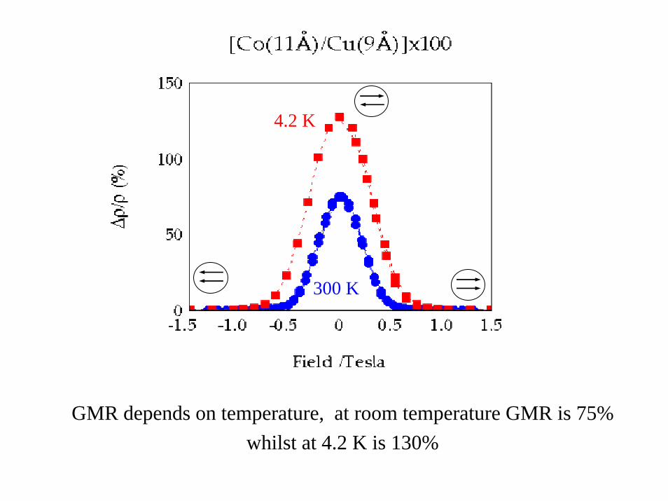
300 K
4.2 K
GMR depends on temperature, at room temperature GMR is 75% whilst at 4.2 K is 130%

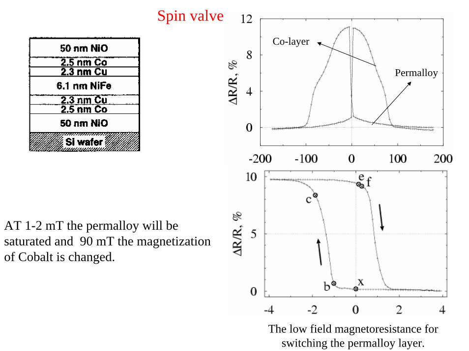
Spin valve
Permalloy
Co-layer
AT 1-2 mT the permalloy will be saturated and 90 mT the magnetization of Cobalt is changed.
The low field magnetoresistance for switching the permalloy layer.

FeMn layer is used to 'pin' the Co layer magnetization in a certain direction. Co layer is used as a reference layer with fix magnetization.NiFe layer, which is very magnetically soft, can now be aligned parallel or antiparallel by very tiny fields. Cu spacer between these two to stop there from being any magnetic coupling between the layers. Ta layers are a buffer (to give a good surface to grow on) and a cap (to stop the sample from being oxidized in air). Si is substrate, the whole sample is deposited on a piece of Si
The GMR active region will be only about 100Å thick, with the whole structure being about 300Å, on top of a 1mm thick piece of Si.
~100 °
A~300 °
A

The symmetry spin valve can also works at low magnetic field.The resistance of symmetric spin valve is 10% in 10 Oe

Wolf 2001

oA100
The Magnetic moment in easy reversed layer lies parallel to the plane of the media in absence of
any applied fields.The magnetic moment in fixed magnetic layer of
GMR is oriented perpendicular to the plane of media.
Read head in magnetic disk recorder
Image from IBM

Non-volatile memories
Sense line: The GMR elements with spin-valve structure that are arranged in series connected by lithographic wires. The sense line stores information.
Word line & Bit line: Source of magnetic field. The fields associated with them is “half select” field. It means the “word” and “bit” magnetic fields combine together in such a way that they produce a field large enough for addressing at the intersection point.


Spin transistorEm
itter
Bas
e
Col
lect
orPositive current
Negative current A strong internal electric field can be present in the heterostructure interface region, which is perpendicular to the layer.This induced spin-orbit effect can rotate the spin of current out of alignment with magnetization of second ferromagnetic pad and decreasing the transmitted current.
Johnson Spin transistor

More applications:
1) The superconductivity can be quenched by injection spin-polarized carrier from ferromagnetic into superconductor.
2) Injection spin-polarized current to two dimentional electron gas channel. The long mean free path electrons yield micrometer-length paths that are free of spin flip scattering.
3) Fabrication of “nonvolatile reprogrammable logic”, with magnetoelectronic elements. Additionally they can remember their function they could be reset with the use of software to serve other function.
It means, a microprocessor chip could be reprogrammed in mid-calculation to reconfigure itself at nanosecond speed merely by reversing the magnetization of some its elements in order to most efficiently address the next part of the calculation.
4) The ability to make increasingly smaller electronic devices and combine dissimilar materials within a device both serve to make spin-polarized effects more important.
Top Related