


Languages
Pages
Legal


Name Designation Affiliation Date Signature
Additional Authors
Submitted by:
L. D’Addario JPL
Approved by:
W. Turner Signal Processing Domain Specialist
SPDO 2011‐03‐26
LOW‐POWER CORRELATOR ARCHITECTURE FOR THE
MID‐FREQUENCY SKA
Document number .................................................................. WP2‐040.090.010‐TD‐002
Revision ........................................................................................................................... 1
Author ............................................................................................................. L D’Addario
Date ................................................................................................................ 2011‐03‐29
Status ............................................................................................... Approved for release
WP2‐040.090.010‐TD‐002 Revision : 1
2011‐03‐29 Page 2 of 37
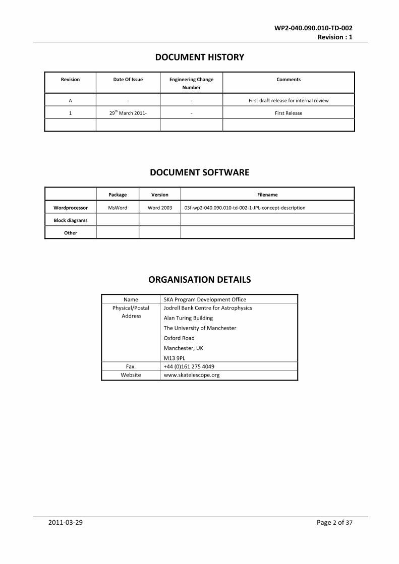
DOCUMENT HISTORY
Revision Date Of Issue Engineering Change
Number
Comments
A ‐ ‐ First draft release for internal review
1 29th March 2011‐ ‐ First Release
DOCUMENT SOFTWARE
Package Version Filename
Wordprocessor MsWord Word 2003 03f‐wp2‐040.090.010‐td‐002‐1‐JPL‐concept‐description
Block diagrams
Other
ORGANISATION DETAILS
Name SKA Program Development Office
Physical/Postal
Address
Jodrell Bank Centre for Astrophysics
Alan Turing Building
The University of Manchester
Oxford Road
Manchester, UK
M13 9PL
Fax. +44 (0)161 275 4049
Website www.skatelescope.org

WP2‐040.090.010‐TD‐002 Revision : 1
2011‐03‐29 Page 3 of 37
TABLE OF CONTENTS
1 INTRODUCTION ............................................................................................. 7
1.1 Purpose of the document ....................................................................................................... 7
2 REFERENCES ................................................................................................ 8
3 INTRODUCTION ..................................................................................... 10
4 CORRELATOR TAXONOMY...................................................................... 12
5 A STRAW‐MAN CORRELATOR FOR SKA‐MID ........................................... 15
5.1 Design Approach ................................................................................................................... 15
5.2 Chip‐Level Constraints .......................................................................................................... 17
5.2.1 Area. .............................................................................................................................. 17
5.2.2 Power. ........................................................................................................................... 17
5.2.3 I/O Rates. ...................................................................................................................... 17
5.3 Processing Element Models .................................................................................................. 18
5.4 Design vs. Architecture ......................................................................................................... 18
5.5 Sharing CMACs Across Frequency Channels ......................................................................... 21
6 ASIC DESIGN DETAILS FOR THE SELECTED ARCHITECTURE ....................... 22
7 SHORTER GATE LENGTH PROCESSES ....................................................... 23
8 CONCLUSIONS ........................................................................................ 23
9 APPENDIX A: MODELING OF SIGNAL PROCESSING ELEMENTS ................ 25
9.1 A1. CROSS‐CORRELATION .................................................................................................... 25
9.1.1 GeoSTAR ........................................................................................................................ 25
9.1.2 ALMA ............................................................................................................................. 25
9.1.3 EVLA .............................................................................................................................. 26
9.2 MEMORY OPERATIONS ......................................................................................................... 26
9.3 . CHIP‐TO‐CHIP COMMUNICATION ...................................................................................... 27
9.4 LONG RANGE COMMUNICATION ......................................................................................... 28
9.5 FILTER BANKS ........................................................................................................................ 28
9.6 BEAMFORMERS ..................................................................................................................... 29
9.7 ANALOG TO DIGITAL CONVERTERS (ADCs) ........................................................................... 29
9.8 LOW NOISE AMPLIFIERS AND OTHER ANALOG SIGNAL PROCESSING ELEMENTS ................ 30
10 APPENDIX B: DETAILS OF ASIC DESIGN CONSIDERATIONS FOR EACH
ARCHITECTURE ............................................................................................ 31
10.1 ARCHITECTURE 1: MATRIX WITH DEDICATED CMAC FOR EACH BASELINE ......................... 31
10.2 ARCHITECTURE 2: MATRIX WITH INPUT DATA BUFFERING ................................................. 32
10.3 ARCHITECTURE 3: MATRIX WITH RAM ACCUMULATORS .................................................... 34

WP2‐040.090.010‐TD‐002 Revision : 1
2011‐03‐29 Page 4 of 37
10.4 ARCHITECTURE 4: PIPELINE WITH DELAYS BETWEEN CMACS ............................................. 35
10.5 . ARCHITECTURE 5: PIPLELINE WITH RAM ACCUMULATORS .............................................. 37
LIST OF FIGURES
Figure 1 Correlator family tree. Distinct architectures are highlighted. #1 was used for ALMA, EVLA,
and SKA Memo 127. #4 is described in [5]. ................................................................................ 12
Figure 2 Top level correlator structures. (a) Matrix, (b) Pipeline. ........................................................ 13
Figure 3 CMAC with accumulator implemented by a dedicated register (top) and using a memory
bank (bottom). ............................................................................................................................ 13
Figure 4 Sharing among frequency channels. Top: Correlator running at rate b, processing a single
channel of bandwidth b. Middle: Correlator running at rate Kb processing K channels by
means of an input buffer. Each sample is written to and read from the buffer once. Buffer can
be separate from correlator. Bottom: Correlator running at Kb and processing K channels by
means of RAM accumulators. Requires N(2N+1)//2N ≈ N writes/reads per sample. RAMs must
be integrated with correlator ICs. .............................................................................................. 22
Figure 5 Block diagram of an ASIC for Architecture 2, showing how it can compute all baselines for
N=2025 antennas at 300 kHz bandwidth (K=3 channels) with 65 ms integrations. Inputs and
outputs are implemented as high speed serial links at achievable rates. (DES=deserializer,
SER=serializer.) ........................................................................................................................... 23
Figure 6 Overall structure of an IC for implementing Architecture 2. .................................................. 32
Figure 7 Overall structure of an IC for implementing Architecture 3. .................................................. 34
Figure 8 An arrangement of 8 ICs for correlating 2N signals. Each IC is capable of correlating N/2
signals (entering from the left) against N/2 other signals (entering from the bottom).
Unlabeled inputs in the diagram receive the same signals as the IC to the left or below. The
first four ICs (A, B, C, D) form a square matrix that is split along the diagonal. The lower
triangular part crosscorrelates all pairs of signals 1 through N, and the upper triangular part
cross‐correlates all pairs of signals N+1 through 2N. The other four ICs (E, F, G, H) correlate
signals 1 through N against signals N+1 through 2N. To accomplish this efficiently, it is
necessary for two of the ICs (A and D) to operate in a different mode from the others. These
accept a total of N signals (including N/2 signals entering from the top and from the right).
Half of its CMACs are used to correlate all pairs of the first N/2 signals, and the other half are
used to correlate all pairs of the other N/2 signals. The self‐correlations (along the diagonal)
require only half of a CMAC each, so they can be computed for both sets of signals by using
only N/2 CMACs. All 8 ICs can be identical, since they all need the same resources and have
the same number of inputs and outputs; A and D are made to operate differently by asserting
a mode control bit. ..................................................................................................................... 35
Figure 9 Architecture 4 (pipeline with delays) block diagram, from [5]. .............................................. 36

WP2‐040.090.010‐TD‐002 Revision : 1
2011‐03‐29 Page 5 of 37
LIST OF TABLES
Table 1 Element Model Parameters for 90 nm Process Technology ................................................... 18
Table 2 Design Parameters for Straw‐Man Correlator in Each Architecture ........................................ 20
Table 3 Summary of Designs by Architecture ....................................................................................... 21
Table 4 Architecture 2 vs. Processing Technology ................................................................................ 24
Table 5 Example of Memory Organisation for Architecture 2 .............................................................. 33

WP2‐040.090.010‐TD‐002 Revision : 1
2011‐03‐29 Page 6 of 37
LIST OF ABBREVIATIONS
AA .................................. Aperture Array
Ant. ................................ Antenna
CoDR ............................. Conceptual Design Review
DRM .............................. Design Reference Mission
EoR ............................... Epoch of Reionisation
EX .................................. Example
FLOPS ........................... Floating Point Operations per second
FoV ................................ Field of View
Ny .................................. Nyquist
Ov .................................. Over sampling
PAF ............................... Phased Array Feed
PrepSKA........................ Preparatory Phase for the SKA
RFI ................................. Radio Frequency Interference
rms ................................ root mean square
SKA ............................... Square Kilometre Array
SKADS .......................... SKA Design Studies
SPDO ............................ SKA Program Development Office
SSFoM .......................... Survey Speed Figure of Merit
TBD ............................... To be decided
Wrt ................................. with respect to

WP2‐040.090.010‐TD‐002 Revision : 1
2011‐03‐29 Page 7 of 37
1 Introduction
The architecture of a cross‐correlator for a synthesis radio telescope with N>1000 antennas is
studied with the objective of minimizing power consumption. It is found that the optimum
architecture minimizes memory operations, and this implies preference for a matrix structure over a
pipeline structure and avoiding the use of memory banks as accumulation registers when sharing
multiply‐accumulators among baselines. A straw‐man design for N = 2000 and 1 GHz bandwidth,
based on ASICs fabricated in a 90 nm CMOS process, is presented. The cross‐correlator proper
(excluding per‐antenna processing) is estimated to consume less than 35 kW.
1.1 Purpose of the document
The purpose of this document is to provide a concept description as part of a larger document set in
support of the SKA Signal Processing CoDR. It provides a ‘bottom up ‘perspective of Correlation using
ASIC technology by exploring the architectural options. In this respect, this document differs from
the other concept descriptions as the prime consideration is the optimisation of power rather than
providing a full correlator concept. No attempt to provide costing or reliability figures is presented.
WP2‐040.090.010‐TD‐002 Revision : 1
2011‐03‐29 Page 8 of 37
2 References
[1] J. Cordes, "Discovery and Understanding with the SKA." SKA Memo 85, October 2006. Available: http://www.skatelescope.org/PDF/memos/memo_85.pdf
[2] R. Schillizzi et al., "Preliminary Specifications for the Square Kilometre Array." SKA Memo 100, December 2007. Available: http://www.skatelescope.org/PDF/memos/100_Memo_Schilizzi.pdf.
[3] R. Escoffier, private communication (email of 29 January 2010) [4] L. Urry, "A Corner Turner Architecture." ATA Memo 14, 17 November 2000. Available:
http://ral.berkeley.edu/ata/memos/memo14.pdf. See also ATA Memo 22, 16 March 2001. http://ral.berkeley.edu/ata/memos/memo22.pdf.
[5] L. Urry, "The ATA Correlator." ATA Memo 73, 16 February 2007. Available: http://ral.berkeley.edu/ata/memos/memo73.pdf
[6] E. Sigman, private communication (April 2010). [7] International Technology Roadmap for Semiconductors (industry group), 2010 Update.
Available: http://www.itrs.net/Links/2010ITRS/Home2010.htm. [8] Xilinx Corp., on-line package thermal analysis tool, available at
http://www.xilinx.com/cgi-bin/thermal/thermal.pl [9] CoolInnovations.com, PN 3-161606U data sheet, available at
http://www.coolinnovations.com/includes/pdf/heatsinks/3-1616XXU.pdf [10] CoolInnovations.com, PN 3-181806UBFA data sheet, available at
http://www.coolinnovations.com/includes/pdf/heatsinks/3-1818XXUBFA.pdf . [11] J. Poulton et al., "A 14mW 6.25Gb/s Transceiver in 90nm CMOS for Serial Chip-to-Chip
Communications." IEEE J. of Solid State Circuits, vol 42 pp 2745–2757, December 2007 [12] G. Balamurugan et al., "A Scalable 5–15 Gbps, 14–75 mW Low-Power I/O Transceiver in 65
nm CMOS." IEEE J. of Solid State Circuits, vol 45 pp 1010–1019, April 2008 [13] HP Laboratories, CACTI software for embedded memory modeling, version 5.3. See
http://www.hpl.hp.com/research/cacti/ and pages linked from there [14] L. D'Addario and C. Timoc, "Digital Signal Processing for the SKA: A Strawman Design."
SKA Memo 25, 2002 August 15 [15] B. Carlson, "The Giant Systolic Array (GSA): Straw-man Proposal for a Multi-Mega
Baseline Correlator for the SKA." SKA Memo 127, August 2010 [16] Excel spreadsheet file 'architectures.xls'. Copy may be requested from the author at
[email protected] [17] M. Tegmark and M. Zaldarriaga, "Fast Fourier Transform Telescope." Phys. Rev. D, vol 79,
2009 [18] Todd Gaier, private communication.
[19] http://www.alma.nrao.edu/development/correlator/
[20] Ray Escoffier, private communication (email of 1/29/2010)
[21] Sterling Witaker, email to Joseph Trinh on 2/5/2010
[22] Brent Carlson, "Requirements and Functional Specification: EVLA Correlator Chip." NRC
Canada, Hertzberg Inst. of Astroph., Dominion Radio Obs., RFS Document A25082N0000.
Revision 2.5, January 20, 2010
[23] Brent Carlson, private communication (email of 7/16/2010).
[24] R. Palmer, J. Poulton, W. J. Dally, J. Eyles, A. M. Fuller, T. Greer,M. Horowitz, M. Kellam, F.
Quan, F. Zarkeshvari, "A 14mW 6.25Gb/s Transceiver in 90nm CMOS for Serial Chip‐to‐Chip
Communications." IEEE Solid State Circuits Conference, 2007.

WP2‐040.090.010‐TD‐002 Revision : 1
2011‐03‐29 Page 9 of 37
[25] B. Richards, N. Nicolici�, H. Chen, K. Chao, D. Werthimer, and B. Nikolić, "A 1.5GS/s 4096‐
Point Digital Spectrum Analyzer for Space‐Borne Applications." IEEE Custom Integrated
Circuits Conference, September, 2009. Available:
http://bwrc.eecs.berkeley.edu/php/pubs/pubs.php/1090/PID882350.pdf
[26] A. Wang, "A 180‐mV Subthreshold FFT Processor Using a Minimum Energy Design
Methodology." IEEE J. of Solid State Circuits, vol 40, pp 310‐319, 2005.
[27] Advanced Optronice Devices, model AODM‐XT154‐LD‐CD‐MF data sheet. Available:
http://www.aodevices.com/pdf/OPC/Module/xfp/AODM‐XT154‐LD‐CD‐MF.pdf.
[28] L. D'Addario, "LWA Fine Delay Tracking." LWA Memo No. 143, 2008 November 10.
Available: http://www.ece.vt.edu/swe/lwa/memo/lwa0143.pdf.
[29] HP Labs, CACTI simulation software for embedded memories. Available:
http://quid.hpl.hp.com:9081/cacti/.
[30] L. D'Addario, Excel spreadsheet 'adc+dacSurvey.xls'.
[31] M. Choi, J. Lee, J.Lee, and H. Son, "A 6‐bit 5‐GSample/s Nyquist A/D Converter in 65nm
CMOS." 2008 Symposium on VLSI Circuits
[32] M. Scott, B. Boser, and K. Pister, "An ultra–low power ADC for distributed sensor networks."
Proc. of 28th European Solid‐State Circuits Conference, ESSCIRC‐2002, 24‐26 Sep 2002.
[33] C. Recoquillon, A.Baudry, J‐B Bégueret, S. Gauffre, and G. Montignac, "The ALMA 3‐bit 4
Gsample/s, 2‐4 GHz Input Bandwidth, Flash Analog‐to‐Digital Converter." ALMA Memo No.
532, 13 July 2005 Université de Bordeaux, "ALMA 3‐bit, 4Gsps Analog‐to‐Digital Converter:
Data Sheet.” Version 1.3, 13 July 2005. Available: http://www.obs.u‐
bordeaux1.fr/electronique/ALMA/Datasheet_Converter.pdf
[34] Leonid Belostotski and James W. Haslett, "Wide Band Room Temperature 0.35‐dB Noise
Figure LNA in 90‐nm Bulk CMOS." IEEE Radio and Wireless Symposium, 2007

WP2‐040.090.010‐TD‐002 Revision : 1
2011‐03‐29 Page 10 of 37
3 INTRODUCTION
Power consumption is a major limitation in the implementation of a very‐large‐N array, where 2N is
the number of signals that must be cross‐correlated (N antennas or stations, each receiving 2
polarizations). When N is sufficiently large, power consumption is dominated by the signal
processing electronics for cross‐correlation, which grows as N2 while nearly everything else grows as
N. In this document, "very large" means N>1000.
It was shown in 2002 [14] that such a correlator (N=2560, bandwidth B=1600 MHz) could be built at
reasonable cost in the technology then current (180 nm CMOS), but in that case the monetary cost
of construction, rather than power consumption, was considered the primary limitation. More
recently, another straw man SKA correlator design was proposed [15] (N=2980, B=1 GHz), but its
architecture leads to an unreasonably high estimated power consumption of 2 MW for the cross‐
correlation electronics alone. Neither of these studies considered the possibility of multi‐beam
antennas, which requires duplicating the correlator for each beam and hence multiplying the power
consumption by the number of beams. Here we show how it is possible to do much better.
At low frequencies, very‐large‐N arrays are generally not needed, even to produce an SKA‐scale
telescope. When wavelength λ is ~1m or more, it is cost effective to use dipole‐like antenna
elements whose size is ~λ/2. Assuming that the objective is to achieve a given survey speed [1], the
optimum design combines many such elements into stations by beamforming so that N is the
number of stations. In this way, N~200 is sufficient to achieve the specifications of SKA‐low (70 to
300 MHz) [2].
As frequency increases, the use of elements ~λ/2 in size becomes rapidly inefficient because
effective area is proportional to λ2 while element field of view remains unchanged. The number of
elements needed to achieve a given survey speed increases as λ–4 and we are soon overwhelmed by
the cost and power consumption of per‐element electronics such as low‐noise amplifiers and
analog‐to‐digital converters. A cost‐effective design then requires elements many wavelengths in
size, such as reflector antennas. As element size d increases, its effective area Ae grows as d2 and
element field of view Ω (beamwidth) decreases as d–2, but the contribution of that element to the
survey speed (proportional to Ae2 Ω) grows as d2, reducing the number of elements needed. Each
element's electronics thus supports more collecting area, so it need not dominate the cost. There is
an optimum element size that depends on a trade off between the cost of the structure needed to
implement the antennas and the cost of the electronics. At present prices, and assuming that cross‐
correlation is not the dominant cost for electronics, reflector antennas with a diameter d between
6m and 18m appear to be optimum. But combining these reflector antennas into stations is not so
effective as it is for dipole‐like elements; this is because their beams are relatively small so they must
be mechanically steered to point at different parts of the sky, and this prevents them from being too
close to each other. Instead of combining them, it is arguably cost‐effective to install multiple feeds
on each reflector so as to create multiple beams, increasing Ω. Thus, even though we have kept the
number of elements from getting too large, we must cross‐correlate nearly all of them. This leads to

WP2‐040.090.010‐TD‐002 Revision : 1
2011‐03‐29 Page 11 of 37
designs for SKA‐mid (300 MHz to 10 GHz) with N=2000 to 3000 reflector antennas [2]. This is the
situation to which the present document applies1.
The main point of this document is that considerable care must be taken in the design of a correlator
for a very‐large‐N array if the power consumption (and perhaps also monetary cost) of that
correlator is not to be a major obstacle to its construction and to the operation of the whole array.
Consider, for example, the correlator for the ALMA telescope, which is the largest radio astronomy
correlator constructed to date. It supports N=64 and bandwidth B=8 GHz. A reasonable measure of
a correlator's size is S=N2B, which is 3.28x10¹³ Hz for ALMA. The cross‐correlation part of this
correlator (not including its per‐antenna processing) uses about 65 kW [3]. Now consider a possible
correlator for SKA‐mid with N=2000 and B=1 GHz, giving S=4.0x10¹⁵ Hz. If we simply extrapolate the
ALMA power consumption in proportion to S, we predict that an SKA correlator built with the same
architecture and technology will use 7.9 MW. If multi‐beam antennas are used, then this must be
multiplied by the number of beams.
It is shown here that the SKA correlator can be built so as to use several orders of magnitude less
power than this. Such a low‐power correlator can be built using current technology, without waiting
for Moore's Law to make it easier. To achieve this, it is necessary to choose the correlator's
architecture carefully.
At its core, a correlator performs multiply‐accumulate (MAC) operations on all pairs of input signals.
The rate at which it does this is N(2N+1)B (assuming complex signals and Nyquist‐rate sampling), and
that rate is the same regardless of architecture. However, a practical correlator must do other
operations as well. In particular, it needs input and output (I/O) operations for external connections
as well as for internal signals (since a large correlator cannot fit in a single device or box), and it
needs memory operations because in most architectures it must store data temporarily in buffers.
Memory and I/O operations typically use much more energy than MAC operations, and their rates
are strongly dependent on architecture.
This document considers only the cross‐correlator proper, ignoring the processing that must be done
on the signals separately before they are combined. This is justified by the assumption that cross‐
correlation is the dominant power consumer at very large N. It is assumed that the per‐signal
processing includes a uniform filter bank so that the cross‐correlation work can be partitioned by
frequency ("FX" style). The cost of re‐ordering samples between the filter banks and the cross
correlator ("corner turner") is also ignored on the assumption that a memoryless corner turner [4]
with negligible power consumption can be used. At the correlator's inputs, each signal is assumed to
be a discrete‐time sequence of coarsely quantized samples, each consisting of the real and imaginary
parts of a complex number. The correlator then performs complex MAC (CMAC) operations.
1 This comparison of SKA-low and SKA-mid has been somewhat simplified because the SKA's science-driven specifications have evolved in such a way that the required survey speed is not constant with frequency, and there are some objectives for which point source sensitivity is a better figure of merit than survey speed. Nevertheless, it turns out that only moderate N is needed at low frequencies and very large N is needed at higher frequencies, where the boundary is near 300 MHz.

WP2‐040.090.010‐TD‐002 Revision : 1
2011‐03‐29 Page 12 of 37
4 CORRELATOR TAXONOMY
Figure 1 provides a classification of correlator architectures as a hierarchical tree. The final nodes,
highlighted in the figure, represent five distinct architectures2. At the top level, we distinguish
between a matrix structure, where MAC elements are arranged in a triangular array, and a pipeline
structure, where MAC elements are arranged in a chain with delays between them; this distinction is
further explained below (see Figure 2). In the matrix structure, it is possible to arrange that each
signal pair (baseline) is connected to a dedicated CMAC.
Figure 1 Correlator family tree. Distinct architectures are highlighted. #1 was used for ALMA, EVLA, and SKA
Memo 127. #4 is described in [5].
This is the first of the architectures (#1). In all the others, each physical CMAC is time‐shared among
baselines so as to reduce the number of CMACs that must be built. This is possible if each CMAC can
operate faster than the signal bandwidth that it is processing. Thus, if the bandwidth processed is b,
where a filter bank has partitioned each antenna element's bandwidth B into multiple channels of
bandwidth b, and a CMAC operates at clock rate f = xb, then that CMAC can be shared among x
baselines.
There are two ways of arranging the sharing of a CMAC among baselines. First, the input samples
from all antennas of the shared baselines can be written to a memory that holds enough samples for
one correlation (i.e., one short‐term integrating time of the correlator). Samples for one pair of
antennas are then read from the memory at rate f and sent to the CMAC.
2 It is not claimed that this classification includes all possibilities, but it is believed to span most of those that involve cross-correlating all signals. It excludes FFT-based methods that achieve a similar result under special circumstances, such as [17].

WP2‐040.090.010‐TD‐002 Revision : 1
2011‐03‐29 Page 13 of 37
Figure 2 Top level correlator structures. (a) Matrix, (b) Pipeline.
Figure 3 CMAC with accumulator implemented by a dedicated register (top) and using a memory bank
(bottom).
At the end of the integrating time, the CMAC's accumulator is read out and then cleared. Then
samples for a different pair of antennas are read from the memory and correlated, continuing in this
way until all x pairs have been correlated. The second method of sharing among baselines involves
providing the CMAC with multiple integration registers, as illustrated in Figure 3 In this method, no
input buffer is required and the samples at the CMAC's inputs can be from a different pair of
antennas on each clock. On each clock, the CMAC reads an accumulation register, adds the product
WP2‐040.090.010‐TD‐002 Revision : 1
2011‐03‐29 Page 14 of 37
of the current samples, and writes the results back to the same accumulation register. On the next
clock, it uses a different accumulation register. The most practical way to do this is to arrange the
accumulation registers in a RAM of depth x and to increment the RAM's address on each clock. After
x clocks, the address returns to its original value and the input signals return to the original antenna
pair, enabling the next product for that baseline to be accumulated. After enough cycles have
elapsed to complete an integration time, results for all x baselines are available in the RAM and can
be read out. The two methods correspond to architectures #2 and #3 in Fig. 1.
In the pipeline structure, essentially the same two methods of CMAC sharing can be used, and these
correspond to architectures #4 and #5 in Fig. 1.
The general pipeline concept [5] involves sending samples from all 2N signals to the chain of CMACs
serially, on a single bus, as shown in Fig. 2b. We transmit a block of samples from the first signal,
followed by a block from the second signal corresponding to the same time range, then a block from
the third signal, etc. The samples are sent to one input of every CMAC at the same time, but they
are delayed by the length of the block before going to the other input of the second CMAC, then
again by the same amount before going to the other input of the third CMAC, etc. In this way, the
first CMAC computes the correlation of each signal with itself; the second computes the cross‐
correlation of all pairs whose index numbers differ by 1; the third does those whose indices differ by
2; etc. To compute correlations for all baselines, the arrangement must be a bit more complicated
that shown in Fig. 2, which is a simplification. Some switches are needed so that each CMAC handles
a different set of baselines for half of the time; see [5] for details. With these switches, a chain of
N+1 CMACs is sufficient to compute correlations for all N(2N+1) pairs. On each clock, N+1 products
are computed in parallel. After all 2N blocks of samples have been received, 2N(N+1)=N(2N+2) sets
of products will have been computed; N of them are redundant. The sharing factor x is thus fixed by
the architecture at 2N.
The difference between architecture #4 and #5 is in the length of the delay between CMACs. In #4,
the delay is equal to the number of samples in one integration, so the block of samples from each
signal must also be of that length. After each block, the accumulators of all CMACs are read out and
cleared. This is similar to #2 in that samples for one integration of all signals are buffered before
cross‐multiplication. This is also the original pipeline architecture, first described in [5]. In
architecture #5, each delay is for only one clock, so it is implemented as a single register. A sample
from a different antenna is received on each clock, and each CMAC has a bank of accumulators
implemented in RAM as in #3. (To my knowledge, this arrangement was first proposed by Sigman
[6].)
For any of the architectures, if the correlator's clock rate is fast enough, then it can also be shared
among multiple frequency channels. We assume that this is done by processing samples from one
channel for one integration time, accumulating results for all baselines, reading out those results,
then processing the same number of samples from another channel. If the clock rate is xKb, then
one CMAC can process x baselines and K channels (or bandwidth Kb) per integration interval.
However, unlike the sharing of CMACs among baselines, we do not regard their sharing among
channels as creating distinct architectures. This is discussed in more detail later (Section 5.5).

WP2‐040.090.010‐TD‐002 Revision : 1
2011‐03‐29 Page 15 of 37
5 A STRAW‐MAN CORRELATOR FOR SKA‐MID
To evaluate the various architectures, consider a hypothetical correlator with these parameters:
• Number of antennas: N ≈ 2000
• Nyquist bandwidth per signal: B = 1.0 GHz
• Channel bandwidth b = 100 kHz
• Beams per antenna: J = 100
• Minimum integrating time: τ = .065 s (bτ = 6500)
• Input sample quantization: ws = 4 (2 bits real + 2 bits imaginary)3.
This is reasonably representative of the requirements for SKA‐mid 4 [2]. The value of J is somewhat
arbitrary and has no effect on the architecture, since a separate correlator must be built for each
beam; we will actually consider a J =1 design and assume that it will simply be duplicated J times.
The integration time τ cannot be too small without making the correlator's output data rate
unreasonably high, but if it is too large then excessively large buffers are needed to hold one
integration of input samples. The ratio of total output data rate of a cross correlator to its total
input rate is given by
(wc/ws)(2N+1)/(2bτ)
where wc is the accumlator word size (bits). For wc = 32 b (16b real, 16b imaginary) and the other
parameters as given above, we are allowing the output rate to be up to 2.5 times the input rate 5.
We will attempt to find practical implementations of this correlator using the five architectures,
considering each separately.
5.1 Design Approach
We begin by assuming that for such a large instrument the basic building block must be an
application‐specific (custom) integrated circuit (ASIC), and that any attempt to build it with general‐
3 In the author's opinion, finer quantization than this is not justified, although ws = 8b (4b+4b) has been proposed for some SKA designs (e.g., [15]). Using the latter would increase the power and IC count by a factor of 3 to 4 in most architectures. A full discussion is beyond the scope of this memo. 4 The actual implementation may be more complicated, since 50% of the antennas are intended to be outside a 5 km diameter core, with non-core antennas having single-beam feeds and being combined into stations of ~5 antennas each. Here N is the total number of stations. With ~3000 antennas altogether, we might want to correlate 1500 core antennas, each with b~100 beams, along with ~300 non-core stations, each with ~20 station beams. This gives N=1800 and J=20 or 100, depending on baseline. Our straw-man parameters, based on a uniform array of individual antennas, are thus somewhat simplified but nonetheless representative. 5 Although this is difficult enough to handle, it could be worse. For long baselines, large τ results in azimuthal smearing in the u,v plane and large b results in radial smearing, so it can sometimes happen that bτ < 6500 is desirable. We assume that this will be handled by making τ smaller on those baselines and larger on others, and keeping b uniform, so that bτ ≥ 6500 on average. In this memo, such complications are ignored.

WP2‐040.090.010‐TD‐002 Revision : 1
2011‐03‐29 Page 16 of 37
purpose hardware like FPGAs, graphical processing units, or microprocessors would at present be
impractical6. The parameters of the ASICs are allowed to be different for each architecture, but to
allow a fair comparison we insist that they all be built using the same process technology. For this
we choose CMOS with 90 nm gate length. That technology is readily available today from various
foundries. It is not at the edge of the current state‐of‐the‐art, where very large integrated circuits
have been built in 65 nm CMOS and some have been built at gate lengths of 45 nm or smaller, but
these more advanced technologies are currently much more expensive. Their availability at
reasonable cost can be confidently predicted for the future [7], but we choose to consider designs
that are practical today.
Although we will not attempt to derive detailed ASIC designs here, it is necessary to work out the
top‐level structure of each one in order to estimate the number required (and hence the total
internal and external I/O) and the power dissipation. In general we try to fit as much processing into
each chip as possible, and to run it at the highest possible clock rate, subject to the constraints
discussed below.
Each ASIC is constructed from three basic components: CMACs, transmitters and receivers (I/O), and
memories. For each of these, we need to know the amount of silicon area that it occupies and the
energy that it uses for each operation. For some memories (but in practice not for the other
elements), static power consumption is also significant and should be taken into account. These
component parameters are obtained by scaling from existing designs, by reference to the literature,
or by modelling, as described in Section 5.3. From these we calculate how many can fit on a chip7 in
each architecture, and how fast the chip can run. This determines how many chips are needed to
implement the entire correlator, and multiplying this by the power per chip gives the system power.
Several things are neglected here. As mentioned in Section 3, we are considering only the cross‐
correlator proper, not the per‐antenna‐element processing that must precede it (LNA, digitizer,
beamformer, filter bank, and signal transmission from remote antennas). We also neglect certain
infrastructure needed for the cross correlator, such as power supply, monitoring, and control
circuits. These can be implemented with off‐the‐shelf parts and should add only a few percent to
the chip count, but they may add as much as 30% to the power consumption. All inter‐chip I/O is
assumed to be implemented in the same way (with high‐speed serial links), even though board‐to‐
board connections might use slightly more energy than chip‐to‐chip connections on the same board.
We do not attempt to estimate the board counts, although they can reasonably be inferred from the
chip counts.
6 Such notions are nevertheless popular because the sequence ASIC, FPGA, GPU, CPU results in monotonically increasing numbers of knowledgeable designers. Eventually, by extrapolation of Moore's Law, construction of the straw-man correlator suggested here might become practical in general-purpose hardware, but by then a larger or more complex correlator is likely to be desired. Because of this, the history of radio astronomy shows that nearly every digital processor that was considered large at the time of its design has been implemented with ASICs. 7 "Chip" and "integrated circuit" (IC or ASIC) are used interchangeably in this memo. Each is assumed to include a silicon die and a package with pins suitable for soldering to a printed circuit board.

WP2‐040.090.010‐TD‐002 Revision : 1
2011‐03‐29 Page 17 of 37
5.2 Chip‐Level Constraints
The processing that can fit within one chip is limited by one of several constraints. We adopt limits
to the chip's overall area, to its power dissipation, and to its the input and output data rates.
5.2.1 Area.
As the area of each chip increases, its cost increases faster because yield is reduced. Nevertheless,
some very large and complex ICs are in production. For example, Nvidia's GeForce GTX 280 GPU (65
nm technology) has a die size of 576 mm2, and Intel's Core i7‐920 processor (45 nm) has a die size of
283 mm2. On the other hand, the ALMA correlator ACIC (250 nm) is 66.4 mm2 and the EVLA
correlator IC (130 nm) is 40 mm2. Somewhat arbitrarily, we adopt 200 mm2 as the maximum ASIC
die size for this study. This is a large chip, so this is an aggressive choice, but it is well within the
present state‐of‐the‐art, albeit relatively expensive.
5.2.2 Power.
A common rule of thumb is that the maximum power that can be dissipated by air cooling of an IC is
1W/mm2. This assumes that dissipation is uniformly distributed across the chip area (no "hot
spots"), which is reasonable in our case but not so for CPU or GPU chips. The Nvidia and Intel ICs
mentioned above have design power limits of 236W and 130W respectively, corresponding to 0.41
W/mm2 and 0.46 W/mm2. However, approaching this limit requires heat sinks that are far larger
than the IC's package, so it might be achieved when there is only one high‐power IC on a board, but
not otherwise. Our system will require many ICs, so we need to be able to package them so that a
significant number can be placed on each board.
Consider this example. Our 200 mm2 die will fit easily into a 42.5 mm square flip‐chip ball grid array
package; such a package is used by Xilinx for its Virtex 6 FPGAs to achieve a thermal resistance of θJC
= 0.1 K/W from the chip to the package case [8]. A matching pin‐fin heat sink 15 mm high [9] then
achieves θCA = 1.1 K/W from case to air with 2.0 m/s (400 ft/min) air flow. If the maximum junction
temperature is 90C and the air temperature is 25C, the maximum dissipation is 65C/(θJC + θCA) =
54.2 W. A small fan integrated with the same heat sink reduces θCA to 0.70 K/W [10], allowing
dissipation up to 81.25 W. This arrangement of ICs and heat sinks could in principle be close‐packed
on a PC board, but a pitch of 70 to 100 mm would be required to allow for board routing and
supporting ICs. This allows at least 16 ICs to fit on a moderate‐size 400 mm square board.
Based on this example, we set our ASIC maximum dissipation to 75W. This is considered
conservative. More sophisticated cooling methods, including heat transfer by liquids or heat pipes,
could allow similar board density while dissipating 100W to 200W per chip.
5.2.3 I/O Rates.
We assume that inter‐chip I/O will use high‐speed serial links at 2 to 10 Gb/s for data transfer.
Transceivers for such links are now commonly included in FPGAs, and embedded designs for ASICs
have been published [11][12]. We choose the maximum input rate and maximum output rate for
our ASIC to be 40 Gb/s (e.g., 8 links at 5 Gb/s for each direction). Rates up to 20 Gb/s per link are
probably feasible in 90 nm CMOS, and higher aggregate rates per chip could be supported, but with

WP2‐040.090.010‐TD‐002 Revision : 1
2011‐03‐29 Page 18 of 37
reasonable board‐level packing of chips the inter‐board connections could be difficult to handle if
the rate per link or the aggregate rate per chip is much higher.
5.3 Processing Element Models
The main processing elements of each ASIC—CMACs, I/O devices, and memories—are modelled
using the parameters given in Table 1. Several memory models are given because, as will be shown
in the next subsection, the various architectures each require a different type and/or size of
memory. Details of the derivation of these parameters are given in Appendix A, which also discusses
other processing elements commonly needed in radio telescopes.
Table 1 Element Model Parameters for 90 nm Process Technology
The energy consumption of a CMAC was derived by scaling from the actual energy used by existing ASICs, accounting for differences between their actual fabrication technologies and our 90 nm CMOS target and for differences between their actual correlation cell design and our 2b+2b complex MAC. Three chips were considered, namely the ASICs designed for the ALMA correlator, the EVLA correlator, and the GeoSTAR satellite. The energies derived were 2.45 pJ, 1.46 pJ, and 1.0 pJ, respectively. We adopted 2.45 pJ for our model. The die area per CMAC was obtained by scaling from the ALMA design. The static power used by a CMAC is assumed to be negligible. For I/O transmitters and receivers, our model uses the results reported in [11]. Since this design was done in 90 nm CMOS, no scaling is needed. Static power is assumed to be negligible. To estimate the die area, I/O is assumed to be performed by serial transmitters and receivers operating at ≤6.25 Gb/s. However, since no more than 7 of each are needed to reach the maximum 40 Gb/s rates, and since a complete transceiver occupies 0.266 mm2 [11], the total die area is <2 mm2 and this is neglected in our calculations. Memories are modelled using the CACTI simulator from HP Labs [13]. This on‐line tool provides detailed simulation results for a variety of embedded memory types in user‐specified sizes, including dynamic power, static power, and die area.
5.4 Design vs. Architecture
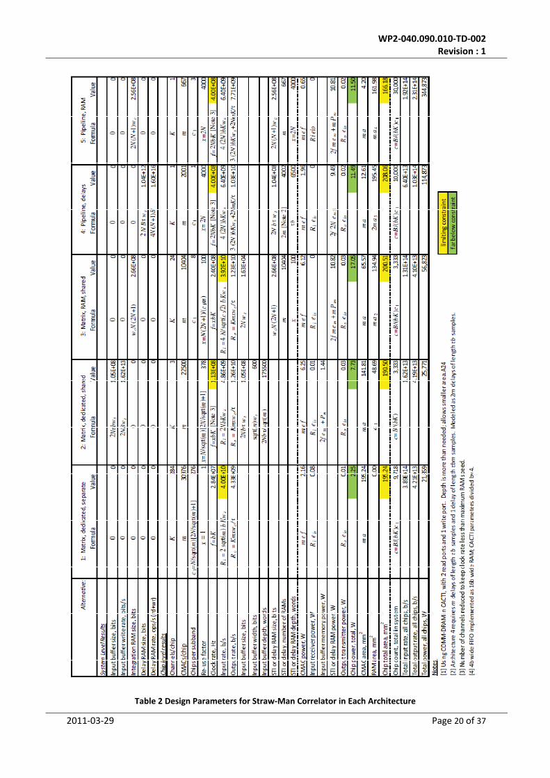
Table 2 is from a spreadsheet [16] that calculates, for each architecture, the parameters of a suitable
ASIC that meets the constraints of Section 5.2 along with the number of ICs needed to construct the
straw‐man SKA correlator (N ≈ 2000, B = 1 GHz). This was done by choosing the number of CMACs
per IC so that those CMACs and the memory devices and I/O needed to support them in a given
architecture will fit within the 200 mm2 die area limit, then setting the clock rate (and hence the
bandwidth per IC) so that the power dissipation is within the 75W limit. An additional, indirect
constraint was imposed for those architectures with embedded memories (2–5): the clock rate
Element (architecture)
Die Area mm2
Energy/op pJ
Static power W
Max. clock MHz
CMAC (all) 0.006303 2.45 0 N/A Transceiver, 6.25 Gb/s (all) 0.266 2.12 0 N/A DRAM 600x177.5k (#2) 48.7 3750 0.593 127 SRAM 32x100 (#3) .0130 1.87 .000143 1165 SRAM 4x6500 (#4) .0488 2.97 .000102 695 SRAM 32x4000 (#5) 0.2428 14.0 .00499 661
WP2‐040.090.010‐TD‐002 Revision : 1
2011‐03‐29 Page 19 of 37
cannot exceed the maximum cycle rate of the memories. Finally, the aggregate input and output
rates of the IC were calculated, and if necessary the clock rate was reduced to bring them within the
constraints. The table also shows the expression used for each calculation. The limiting constrains
are highlighted, as are results that fell far below the applicable constraint. Table 3 is a summary of
the main results.
For the matrix architectures (#1–#3), the number of CMACs per IC was constrained to be square,
resulting in the number of antennas N that can be processed by an integer number of ICs being
slightly more than 2000 (see Table 3).
If we could devote all of the 200 mm2 of die area to CMACs, we would have room for more than
31,000 of them. While that is a large number, it does not approach the 8 million needed to cross‐
correlate N=2000 antennas. Thus for Architecture 1, which has a dedicated CMAC for each baseline,
it is not possible to handle all baselines within one IC. But for all the others, where CMACs are
shared among baselines, we attempted to process all baselines in each IC. Doing so minimizes I/O by
enabling every input sample to be routed to one and only one IC. This is in principle possible
because each IC needs to process only a small part of the bandwidth (as little as one channel). It
turns out, however, that we are not able to achieve this within the 200 mm2 limit for Architecture 3
nor for 5, and we were just barely able to do it for Architecture 4. Architectures 3 and 5 use RAM
accumulators, which take up most of the die area, limiting the number of CMACs that can be
accommodated. Architecture 4 requires a RAM delay buffer for each CMAC, also dominating the die
area. For all architectures, the die size constraint was limiting (i.e., as much area as possible was
used).
For all architectures, the power dissipated by each IC remained far below the 75 W maximum
because some other limit was reached first. For #1 this was the input rate, which reaches 40 Gb/s
at a clock frequency of 28.4 MHz due to the large number of CMACs (1762=30976). Consequently,
the power dissipated is only 2.25 W. For #3, it was also the input rate. For #2, #4, and #5, the clock
frequency was limited by the speed of the memories.
Architecture 1 results in the lowest system power. Since a CMAC is dedicated to each baseline, it
requires no memory for buffering. It does require the most I/O, mostly for input, because the same
sample must be transmitted to many ICs. For all the others, the additional power results almost
entirely from memory operations; I/O power was in all cases negligible8. The pipeline architectures
(#4 and #5) use the most power, and also require the largest numbers of ICs. Those architectures
are intrinsically less flexible because the re‐use factor for each CMAC is fixed at 2N, even when the
CMACs to process all baselines are split among multiple ICs.
In Architectures 3, 4, and 5, the ASIC is dominated by memory, which uses 67%, 94%, and 98% of the
die area and 64%, 83%, and 94% of the power, respectively, hence their high power consumption.
8 This suggests that we could do better by relaxing the I/O rate constraint, but remember (Section III.B.3) that the 40 Gb/s limit resulted from a concern about the feasibility of board-level interconnections rather than IC power dissipation. A 25-IC board would have 1 Tb/s of input or output at 40 Gb/s per IC.
WP2‐040.090.010‐TD‐002 Revision : 1
2011‐03‐29 Page 20 of 37
Table 2 Design Parameters for Straw‐Man Correlator in Each Architecture

WP2‐040.090.010‐TD‐002 Revision : 1
2011‐03‐29 Page 21 of 37
Table 3 Summary of Designs by Architecture
In Architecture 2, memory accounts for 26% of the die area and 19% of the power. The input buffer
is implemented as a single large memory, and it is constructed as dynamic RAM in order to achieve
high density in spite of a penalty in speed and static power compared with static RAM. Its system
power is 18% higher than for #1 (which has no memory) but it uses 1/3 the number of ICs and has
61% less total I/O rate per IC. In this memo we have so far ignored monetary costs, concentrating
instead on power consumption, but the smaller number of ICs (and hence of boards and
interconnections) and lower I/O rate have a significant cost impact, and this is judged to be well
worth the small increase in power over Architecture 1. For that reason, Architecture 2 is considered
the best choice for our straw‐man correlator, at least for an implementation in 90 nm CMOS under
the adopted constraints.
A more detailed discussion of the design considerations for each architecture is given in Appendix B.
5.5 Sharing CMACs Across Frequency Channels
The results in Section 5.4 assumed that each CMAC can process more than one frequency channel by
running at clock frequency xKb, where x is the factor by which each CMAC is re‐used for multiple
baselines and K is the number of frequency channels it processes. K was chosen to maximize the
clock rate while achieving all constraints (power dissipation, I/O rates, and memory speed). The
CMACs can thus be shared among frequency channels, as well as among baselines. However, unlike
sharing by baselines, sharing by frequency channels does not result in distinct architectures.
One way to share among frequency channels is by using a RAM accumulator for each CMAC (see Fig.
3). This requires adding RAM accumulators of depth K to every CMAC in Architectures 1, 2, and 4
and expanding the size of those in Architectures 3 and 5 by a factor of K. However, this would
always be a poor choice compared with the alternative, which is to buffer τb samples (one
integration) for each frequency channel of each signal and deliver those samples to the cross

WP2‐040.090.010‐TD‐002 Revision : 1
2011‐03‐29 Page 22 of 37
correlator, one channel at a time. When the correlator has processed one integration for all
baselines and one channel, and the resulting visibilities have been read out, the samples for the next
channel are delivered, continuing until all K of the shared channels have been processed. The
correlator can do this by running K times faster than it would if all channels were processed in
parallel. This is illustrated in Figure 4.
The required buffering for this purpose is very different from the buffering implemented inside the
correlators of Architectures 2–5. This is because it is implemented for each signal (unlike the
memories in Architectures 3–5, where there is one for each CMAC) , and because each sample is
written to the buffer and read from the buffer only once (unlike the memory in Architecture 2,
which is read multiple times). Therefore the rate of writes and reads is proportional to N. The
buffers can be implemented independently from the cross correlator and we therefore consider
them to be part of the per‐signal processing (F part of an FX correlator).
Figure 4 Sharing among frequency channels. Top: Correlator running at rate b, processing a single channel of
bandwidth b. Middle: Correlator running at rate Kb processing K channels by means of an input buffer. Each
sample is written to and read from the buffer once. Buffer can be separate from correlator. Bottom:
Correlator running at Kb and processing K channels by means of RAM accumulators. Requires N(2N+1)//2N ≈
N writes/reads per sample. RAMs must be integrated with correlator ICs.
The RAM accumulator approach requires a write and read rate proportional to N2, and the RAMs
must be integrated with the cross‐correlation ICs. This would not increase the write/read rate for
Architectures 3 and 5, which already have RAM accumulators, but it would increase the sizes of
those RAMs by factor K, and this would limit the CMACs to a tiny fraction of each IC. (This is moot
for #5, which already is limited to K=1 for other reasons and where the CMACs already occupy only
2.5% of the IC.) For architectures 1 and 2, the extra writes/reads would have a severe impact on
power and the RAMs would dominate the die areas of their ICs, unlike the situation without RAM
accumulators.
6 ASIC DESIGN DETAILS FOR THE SELECTED ARCHITECTURE
A block diagram of an ASIC for Architecture 2, based on the parameters in Table 2, is shown in Figure
5. Its two major components are a 600b wide by 177,500 word deep (106.5 Mb) DRAM and a
150x150 CMAC array. By re‐using the CMAC array 378 times (re‐reading data from the DRAM each
time), it can compute all baselines for N=2025 antennas. When operated at clock frequency f = 113

WP2‐040.090.010‐TD‐002 Revision : 1
2011‐03‐29 Page 23 of 37
MHz, it can do this for 3 channels of 100 kHz each. The DRAM is large enough to buffer 65 ms of
samples from all antennas for one channel (bτ = 6500 samples), and the results can be read out
using a 12.6 Gb/s serial transmitter (or several slower serial transmitters).
The same IC could be used to support a different number of antennas and different integrating time,
provided only that the DRAM has sufficient capacity. Details are determined only by the way in
which the memory is organized. This is controlled by logic that generates the appropriate sequence
of read and write addresses. Although this logic could easily be included in the ASIC using negligible
resources, locating it off‐chip in programmable logic (as illustrated in Fig. 5) makes the ASIC more
flexible and usable in a variety of projects.
7 SHORTER GATE LENGTH PROCESSES
Table 4 shows how the results for Architecture 2 might change in future (and past) technologies,
including 65 nm and 32 nm gate lengths. The memory parameters were again obtained from CACTI
[13] and the other parameters were scaled from their 90 nm values. Only the number of CMACs per
IC and the number of frequency channels processed were adjusted in order to meet the constraints.
The constraints were kept the same, except that the I/O rate was allowed to double (to 80 Gb/s) in
32 nm technology. This predicts that, at 32 nm, the correlator could be constructed with 556 ASICs
and 5.5 kW of dissipation per beam. It also shows that in older technologies it would have been very
difficult to process all baselines in a 200 mm2 IC, and that in 250 nm CMOS it would also have been
necessary to reduce the channel bandwidth below 100 kHz in order to achieve a feasible clock rate;
the sample design for 250 nm would require 160,000 ICs and dissipate 848 kW.
Figure 5 Block diagram of an ASIC for Architecture 2, showing how it can compute all baselines for N=2025
antennas at 300 kHz bandwidth (K=3 channels) with 65 ms integrations. Inputs and outputs are
implemented as high speed serial links at achievable rates. (DES=deserializer, SER=serializer.)
8 CONCLUSIONS
It has been shown that minimizing power consumption in a cross correlator requires choosing an
architecture that requires few memory operations. This means that the use of RAM accumulators
should be avoided, and that the matrix structure is much better than the pipeline structure.

WP2‐040.090.010‐TD‐002 Revision : 1
2011‐03‐29 Page 24 of 37
Reasonable power (<35 kW/beam) for N=2000 and B=1 GHz can be achieved in 90 nm CMOS. This is
about 200 times less than it would be if built with the architecture and technology used for the
ALMA correlator, the largest radio astronomy correlator to date.
Table 4 Architecture 2 vs. Processing Technology

WP2‐040.090.010‐TD‐002 Revision : 1
2011‐03‐29 Page 25 of 37
9 APPENDIX A: MODELING OF SIGNAL PROCESSING ELEMENTS
Sections 9.1–9.3 of this Appendix explain how the technology parameters in Table 1 were obtained
for CMACs, memories, and I/O. Sections 9.4–9.8 discuss the energy and power used by other signal
processing elements that multi‐antenna radio telescopes often require, including long‐distance
signal transmission, filter banks, beamformers, analog‐to‐digital converters, and low noise
amplifiers.
9.1 A1. CROSS‐CORRELATION
9.1.1 GeoSTAR
The GeoSTAR project has a correlator chip design for which a prototype has been fabricated but not
completely tested [18]. It is implemented in a 90 nm CMOS process and operates on a 1.0V supply.
It includes 289 complex multiply‐accumulate cells (1 each CMUL, CADD, and CWREG) operating on
2b+2b samples. Simulations show that each cell9 uses 1.0 mW at 1 GHz clock [21], or 1.0 pJ per
complex multiply‐accumulate operation
9.1.2 ALMA
The ALMA correlator uses an XF style and includes ASICs that compute 4096 lags (1 each real
multiply, real add, real register write, and delay) at 125 MHz and 2b per sample [19]. The chips are
built in 250 nm CMOS and operate at 1.8V. Each lag cell includes a 20b accumulator and a 16b
readout register. We do not have accurate power data at the chip level, but the chips are organized
into 64‐chip boards and there are 512 boards in the system. The total power consumption of all
boards is 65 kW [20]]. That includes on‐board dc‐to‐dc converters (but those should have
efficiencies of more than 90%) and a few smaller control chips. From this we find that each chip
uses about 1.98W, or 484 μW per lag, or 3.9 pJ per operation. Each chip takes input streams for 8
antennas and sends 8 similar (delayed) output streams to adjacent chips on the board. Since the
number of lags far exceeds the number of I/O signals, we can safely assume that I/O uses a negligible
fraction of the power.
The lag cell operates on real numbers. The equivalent complex correlation cell includes a complex
multiply (4 real multiplies and 2 real adds), a complex add (2 real adds), a register write (2 real
register writes), and a delay of 1 clock (2 real delays). We make a rough guess that the overall
scaling factor for energy is 3.5, giving 13.6 pJ per operation for an equivalent complex correlation
cell.
Next we scale the g = 250 nm gate length technology to 90 nm. Ideally, such scaling results in
multiplying all currents and voltages by the same factor as the gate length, resulting in a power ratio
equal to the square of the length ratio for the same clock frequency. But it is difficult to operate at a
supply voltage much below 1V (as shown by the GeoSTAR design). So we scale the voltages only by
0.9V/1.8V, but we scale the currents by 90nm/250nm, giving a predicted energy of 2.45 pJ per
complex correlation if the ALMA design were implemented in 90nm CMOS. This is remarkably close
9 The GeoSTAR design implements a complex correlation cell as 4 real multiply-accumulators, and their literature counts each real MAC as a "correlation cell." Our power per cell is thus 4 times theirs. This includes two more accumulators than necessary, so our value is an overestimate.

WP2‐040.090.010‐TD‐002 Revision : 1
2011‐03‐29 Page 26 of 37
to the nearly‐equivalent value for the GeoSTAR chip, being less than a factor of 3 higher. The ALMA
design is about 8 years older. Low power was a primary design consideration for GeoSTAR, but not
for ALMA.
The ALMA chip size is 8.0 mm x 8.3 mm (66.4 mm2), and each of its 4096 MAC cells contains a 2b x
2b multiplier, 20b accumulation register, and 16b readout register. The registers probably occupy
most of the cell area, but if we conservatively assume that they are 50% of the area then the
corresponding CMAC cell has 3.0 times its area (4 multipliers and 2 accumulators). Neglecting die
area used by control circuits and pads, this gives an area per CMAC cell of (3.0/3096)(66.4 mm2) =
.04863 mm2. Scaling to 90 nm in proportion to g2 gives a CMAC die area of .0063028 mm2.
9.1.3 EVLA
The EVLA correlator also uses an XF style and is based on an ASIC [22] built in g = 130 nm CMOS [23].
It computes 2048 complex lags from real inputs at 256 MHz and 4b/sample, where each cell is based
on a VLBI‐style architecture. This makes it a bit difficult to compare with other complex correlators.
The "core" power consumption is 1.88W at 1.02V; an additional 0.7W is used by "I/O," on a separate
2.5V supply. The chip accepts 16 real input signals and delivers delayed versions to 16 outputs. The
design was frozen in 2005, and the die size is 5x8 mm .
Based on the reported core power only, this gives an energy per complex multiply‐accumulate of
3.586 pJ. Full complex multiplication would require 3 additional multipliers. On the other hand, its
4b multiplication is about 4 times more complex than 2b multiplication; and fringe rotation circuitry
could be deleted. Other components, especially the accumulators, would be unchanged. My guess
is a net power reduction by 2/3 for 2b, full complex correlation. Scaling to 90 nm technology at 0.9V
gives a final scaled energy of 1.46 pJ per 2b complex correlation.
Assuming that the accumulators in the EVLA correlation cell use 50% of its die area, the main
multiplier uses 25%, and the fringe rotation circuitry uses 25%, the 2b/sample CMAC cell should
require 0.5625 times its area. (The accumulators are unchanged, the multiplier is duplicated 4 times
but each is 16 times smaller, and the fringe rotation is eliminated.) Ignoring the area used by control
circuits and pads, and scaling by g2 to 90 nm, this gives a CMAC die area of
(40mm2/2048)(0.5625)(90/130)2 = .005266 mm2. This is remarkably close to the value obtained by
scaling the ALMA chip.
9.2 MEMORY OPERATIONS
We begin by considering a couple of commercially available memory chips, based on their published
data sheets. These may not be particularly representative choices.
Synchronous static RAM, Cypress CY7C1062DV33. This is a 8Mx8b "QDR" device (double data rate,
separate read and write ports) that operates at 1.8V and 350 MHz clock, giving an effective I/O rate
of 700 MB/sec (reads and writes). It draws a maximum current of 825 mA, for a power of 1.485W
and an energy of 2.12 nJ per 8‐bit word written or read.
Synchronous dynamic RAM, Hynix H5TC1G83TFR‐H9A. This is a 128Mx8b DDR3 device, operating at
1.35V and 667 MHz clock, for an effective I/O rate of 1.333 GB/s. It draws 95 mA during either read
WP2‐040.090.010‐TD‐002 Revision : 1
2011‐03‐29 Page 27 of 37
or write operations at this rate, giving 96 pJ per 8‐bit word. While this device is no doubt
implemented in a more advanced technology than the SRAM above, that is not enough to explain
the factor of 22 lower energy.
ASIC‐based signal processing discussed in this documentimplements memory inside the processing
chip rather than separately. Detailed power estimates can be computed using the CACTI simulation
tool [28]. Here are two examples of results, both in 90 nm technology:
Embedded Static RAM, 4K x 8b: 8.24 pJ per operation, negligible static power.
Embedded Dynamic RAM, 2M x 32b (64 Mb): 1.16nJ/operation (291 pJ/byte, 146 pJ per 2b+2b
sample), plus 0.12W of static power.
All values in Table 1 of the main text are obtained by separate runs of CACTI for the specific sizes
given there. Other CACTI input parameters included:
• Number of banks: 1
• Ports: 1 read/write port for all SRAMS; 2 read ports and 1 write port for DRAM.
• Temperature: 350 K (77 C).
• Transistor types: all optimized for low operating power, except that the RAM cells in
the DRAM used the "COMM‐DRAM" type because this produced smaller die area.
• Interconnection type: "conservative".
• Wire type outside mat: "semi‐global".
9.3 . CHIP‐TO‐CHIP COMMUNICATION
A 6.5 Gb/s transceiver using 13.8 mW was demonstrated in 90 nm, 1.0V CMOS [24]. It includes a PLL
clock multiplier and 8x serialization/deserialization. The power is equivalent to 2.12 pJ per bit
transferred. It breaks down into 0.75 pJ/bit for the transmitter (SER+XMT), 1.23 pJ/bit for the
receiver (RCV+DES), and 0.55 pJ/bit for the shared clock. An independent transmitter and receiver
(separate clock PLLs) would thus use 1.3 pJ/bit and 1.78 pJ/bit, respectively or 3.08 pJ/bit total. On
the other hand, a chip with multiple receivers or multiple transmitters (but no transceivers) could
share its clock PLL among the channels. In our models, we use assume that the clock is shared
between two or more modules in each chip. We use the full 2.12 pJ/bit for each transmitter and
each receiver, so that it includes the energy of the device at the other end of the link.
The Xilinx RocketIO modules provide another data point. According to the Xilinx Power Estimator
(http://www.xilinx.com/ise/power_tools/license_virtex6.htm), a 5 Gbps transceiver on a Virtex 6
"low power" device (40 nm technology) uses 0.2355 W, or 47.1 pJ/bit. It is not clear why this is so
much larger than the value we get from [24].

WP2‐040.090.010‐TD‐002 Revision : 1
2011‐03‐29 Page 28 of 37
9.4 LONG RANGE COMMUNICATION
For transmission between boards within the same room, somewhat higher energies per bit might be
needed, but that is ignored in this memo. We assume that the same transceivers and the same
energy per bit as for inter‐chip communication on the same board.
For longer range transmission, such as between an antenna station and a central processing facility,
we assume high‐speed serial transmission on optical links. A digital serializer, transmitter, receiver,
and deserializer are still needed, similar to the on‐board chip‐to‐chip case considered above. The
transmitter output then drives a laser modulator and diode laser, and the optical signal is received
by a photodetector and transimpedance amplifier. A typical COTS module containing these
components and operating at 10 Gbps uses 1.32W [27], or 132 pJ/bit. We thus estimate 135 pJ/bit
total for such long‐range transmissions.
Single‐mode fiber can transmit a 10 Gbps signal for 20 to 40 km. Beyond that, optical amplification
and possibly signal regeneration are needed.
9.5 FILTER BANKS
Assume a polyphase structure, with an FIR pre‐filter followed by an FFT. For K channels at input
bandwidth B, the operation rates are
r1 = LB
and
r2 = (B/2) log2K
where L is the FIR length, r1 is the rate of FIR element operations, and r2 is the rate of FFT butterfly
operations. The FIR element consists of two real multiplications, one complex addition, and one
register write and read, which is about 1/2 of a CMAC operation. The FFT butterfly (radix 2) consists
of a complex multiplication, two complex additions, and two reads and writes to RAM. The butterfly
is by far more complex. Typically L is small (4 to 8) and need not vary with K. Therefore, when
K>256 or so, the butterfly operations dominate the power use (and also the chip area). We can then
neglect the FIR operations for the purposes of this estimate.
Richards et al. [25] have described an ASIC in 90 nm CMOS that implements a 4096‐channel
spectrometer for 750 MHz bandwidth real signals. It uses an L=4 pre‐filter and a K=8192 complex
FFT and supports a sampling rate of 1500 MHz using P=0.71 W, of which about 0.1W is static power.
Ignoring the pre‐filter, this gives an energy per butterfly of (P–Pstatic)/r2 = 2(P–Pstatic)/(B log2 K) =
62.6 pJ.
Interesting work using sub‐threshold CMOS to build a very‐low‐power (but slow) FFT has also been
reported [26].

WP2‐040.090.010‐TD‐002 Revision : 1
2011‐03‐29 Page 29 of 37
9.6 BEAMFORMERS
A beamformer sums signals from multiple antennas with each separately delayed and weighted. A
beamformer elementary unit consists of an adjustable delay and adder. We consider two designs
for the adjustable delay: frequency domain and time domain.
The frequency domain design applies only when the signal has already been analyzed into frequency
channels by a filter bank. Delay τ is then implemented by shifting the phase of each channel by φi =
2πfiτ, where fi is the centre frequency of the ith channel. This is accomplished by multiplying each
sample by exp(j2πφi). For this to be accurate, the channelization must be fine enough so that the
phase change from one channel to the next is small: |2π (fi – fi‐1) τ| 1. It is often desirable to
weight the amplitudes of the antennas differently before combining, in which case we multiply by
ai exp(j2πφi). In any case, the effort required is one complex multiplication per sample. The product
is then added into the partial sum from the previous antenna's beamformer element and the new
partial sum is sent to the next beamformer element. We assume an architecture in which the
coefficients ai exp(j2πφi) have been pre‐computed and stored in a RAM table, so the effort also
includes one RAM read operation per sample. The complete element is than a read, complex
multiply, and complex add, which is similar to a CMAC except that no write to an accumulator is
needed. Here, however, we assume that the coefficients are represented as 4b+4b numbers (more
precisely than the 2b+2b samples) and that the adding chain uses 8b+8b numbers. At the final
output of each beamformer, the result is re‐quantized to 2b+2b. By analogy with the CMAC (see
sections 1 above), for which we estimated 1.0 to 2.45 pJ, we now estimate that the multiply and add
operations of a frequency domain beamformer element use 4 pJ/sample. From the embedded static
RAM result in section 9.2 above, we use 8.24 pJ for each RAM read. This gives 12 pJ for each
elementary operation of a frequency domain beamformer.
The time domain design is needed if beamforming is to be done on wide‐bandwidth signals. In this
case, a FIFO buffer is used to implement the part of the delay that corresponds to an integer number
of samples, and the remainder (fraction of a sample) is implemented using an FIR interpolating filter.
The FIFO energy is that of one write and one read to a RAM. The interpolating filter consists of two
identical real‐coefficient filters operating on the real and imaginary sample streams. For filter length
L, this involves 2L real multiplications and 2L real additions. We assume 2b samples but 8b
coefficients and 8b adders. We assume an architecture in which each coefficient is stored in a
dedicated register. Each real multiply‐add is about 1/4 the effort of a complex multiply‐add, so we
can estimate the energy required by analogy to a CMAC (section 9.1 above). The higher precision
arithmetic costs about a factor of 4 in energy, and no write back to an accumulator is needed, so we
estimate that 2.0 pJ/sample is the energy for one stage of the filter. Calculations done for another
project [28] show that L=18 is usually adequate, giving 72 pJ for the filter. The FIFO's RAM can be a
small embedded SRAM; from section 9.2 above, we use 8.24 pJ (write+read, 2b+2b sample). We
thus get a total of 80 pJ for each elementary operation of a time‐domain beamformer.
9.7 ANALOG TO DIGITAL CONVERTERS (ADCs)
In a survey of COTS ADCs completed in November 2009 [30], the lowest energy per conversion found
was 530 pJ. This was for the National ADC08B3000, which is an 8b converter capable of 3 GSa/s. Of
all devices with 8b or less resolution and maximum rate less than 500 MHz, the lowest conversion

WP2‐040.090.010‐TD‐002 Revision : 1
2011‐03‐29 Page 30 of 37
energy was 900 pJ for the Analog Devices AD9288‐100, a dual 8b device with 100 MSa/s maximum
rate. The lowest resolution device found was the Maxim MAX105, dual 6b at 800 MSa/s; it uses 1.34
nJ per conversion.
Some recent papers suggest that better results are possible. A 5 GSa/s, 6b flash converter in 65 nm
CMOS [31] is reported to use 320 mW or 64 pJ per conversion (excluding output buffers and with no
output demultiplexing). A 100 kSa/s, 8b successive‐approximation converter in 250 nm CMOS [32]
uses 3.1 μW or 31 pJ per conversion. The (somewhat older) ALMA ADC, 3b at 4 GSa/s [31][32] uses
1.4W or 350 pJ per conversion; it is built using a 250 nm BiCMOS/SiGe process.
Usually lower resolution is more appropriate for converting Gaussian noise in radio telescopes.
Assuming a flash architecture, the energy per conversion should scale approximately as 2k for k bits.
This applies to the converter proper, but not necessarily to associated circuitry such as code
conversion, demultiplexing, and output pin drivers; these should scale as k, and for many of the
COTS chips these may be dominant. If the ADC is embedded in an ASIC, the output pin drivers are
avoided and the other auxiliary circuits should not dominate the power. As a guess, we'll assume
that half of the energy in a stand‐alone ADC scales as k and half scales as 2k, leading to the following
scaling factors relative to k=8: k=2, 0.266; k=3, 0.406; k=4, 0.562.
We are assuming that most of our digital processing operates on complex signals, but in many
(though not all) radio telescope designs the signals are real at the point of digitization. We are
interested in a wide range of digitization bandwidths, from ~30 MHz to ~10 GHz. For this study, we
are attempting to normalize the energy cost to 90 nm technology.
In view of all these considerations, we adopt the following nominal value for the conversion energy.
Start with the result in [31]; scale to 90 nm technology, obtaining (90/65)64pJ = 88.6 pJ; scale to 3b
resolution, obtaining 66.5 pJ; double to account for auxiliary circuitry, obtaining 132.9 pJ. Since the
power reported in [31] excludes output buffers, this is appropriate for an ADC that is embedded in
an ASIC with the initial stages of digital processing, such as a filter bank.
9.8 LOW NOISE AMPLIFIERS AND OTHER ANALOG SIGNAL PROCESSING ELEMENTS
Unlike most other processing elements, the power used by an LNA depends weakly (if at all) on its
bandwidth. It does depend on the operating frequency range and operating temperature (especially
whether it is cryogenic or not), and it depends strongly on the gain required and the implementation
technology (including not only feature size but also semiconductor type). Here we concentrate on
LNAs intended for room temperature operation at frequencies from VHF to low microwave (30 to
3000 MHz).
If we assume that we want at least V volts rms at the ADC input, then the total gain from the
antenna must be

WP2‐040.090.010‐TD‐002 Revision : 1
2011‐03‐29 Page 31 of 37
where RL is the ADC's input resistance, Tsys is the system temperature and B is the bandwidth. For V
= 10 mV, RL = 50 ohms, Tsys =1000K, and B = 100 MHz, this gives 62 dB. At low frequencies, the ADC
may present a larger RL to the final amplifier stage, reducing the required gain by 10 to 15 dB. At
high frequencies, the signal may be downconverted so that much of the gain is at IF or near
baseband. In any case, producing sufficient gain requires substantial power. We concentrate on the
simplest case where all gain is at RF and the RF band is directly digitized. An LNA with 3 stages is
usually required in order to get >60 dB of stable gain.
There is a shortage of information about LNAs for which low power was a major design
consideration. One recent paper [33] reports a single‐stage LNA for 700‐1400 MHz that uses 45 mW
to achieve about 20 dB of gain. Using 3 of these in cascade to achieve 60 dB thus consumes 135
mW. So far we have not found anything better. For our present models, we adopt the optimistic
assumption that ~10 mW per 20 dB stage can be achieved, giving 30 mW for everything that
precedes the ADC.
10 APPENDIX B: DETAILS OF ASIC DESIGN CONSIDERATIONS FOR EACH ARCHITECTURE
10.1 ARCHITECTURE 1: MATRIX WITH DEDICATED CMAC FOR EACH BASELINE
Figure 2(a) illustrates a correlator for N antennas using Architecture 1, where each box containing
m = n2 CMACs represents one IC. Each signal pair has a dedicated CMAC. The number of ICs
required in the triangular array is (N/n)(2N/n + 1).
For the ICs on the diagonal, only n(n+1)/2 of the CMACs are needed, so there is an inefficiency that
becomes significant if N/n is small. The results in Table 2 and Table 3 include this inefficiency by
assuming that all CMACs are active. We could do better by providing control circuitry that turns off
the unneeded CMACs for those ICs that are on the diagonal. In principle, it would be possible to
make full use of all CMACs by providing the ICs with additional modes in which the CMAC array is
split along the IC's diagonal, with separate input signals connected to the lower and upper triangles.
Along the IC's diagonal, each CMAC would be split into two parts, each doing autocorrelations and
producing real results. This would require doubling the input bandwidth, but Table 2 shows that
input rate is a limiting constraint; without that constraint, we could operate at much higher clock
rate and thus process more bandwidth without dissipating too much power. Pending a detailed
design to establish feasibility, we forego such complexities for the calculations of this documentand
instead accept the inefficiency of having some unused CMACs.
Because no on‐chip RAM is required in Architecture 1, there is room for more CMACs than in the
other architectures. This is its main advantage. Its main disadvantage (for power consumption) is
that it requires more I/O because copies each input sample must be delivered to 2N/n+1 chips.
Fortunately, according to our models, the power used by that extra I/O is small compared to that
used by the CMACs (4.2%, see Table 3). Consequently it achieves the lowest system power
consumption of all the architectures. Another disadvantage is that the input rate limit requires
running at a clock frequency well below the speed of the logic, and also well below what could be
supported by the power dissipation limit. The result is that a relatively large number of chips is
required for the N≈2000 system.

WP2‐040.090.010‐TD‐002 Revision : 1
2011‐03‐29 Page 32 of 37
10.2 ARCHITECTURE 2: MATRIX WITH INPUT DATA BUFFERING
Figure 2(a) also illustrates a correlator in Architecture 2, except that there is only chip with n2
CMACs and each box in the figure represents its re‐use for a different set of input signals. To process
all 2N inputs, it must be re‐used x = (N/n)(2N/n + 1) times. The same inefficiency discussed for
Architecture 1 occurs when one of the blocks on the diagonal of the triangular matrix is being
computed.
Re‐use is accomplished by having τb samples (enough for one integration) from all 2N inputs stored
in an on‐chip buffer memory, as shown in Figure 6. The required memory size is thus M = 2Nτbws
bits, and the clock rate must be at least xb.
The IC operates as follows. On one clock, samples for 2n signals, all for the same sampling time, are
read from the memory; n are delivered to the all CMACs in each row of the array, and n others (in
general different but sometimes the same as the first n) are delivered to all CMACs in each column.
Each CMAC computes the corresponding product and adds it to its accumulator. On the next clock,
samples for the next sampling time of the same 2n signals are read and delivered in the same way,
continuing until all τb samples of those 2n signals have been processed. At that point, the results in
all CMAC accumulators are copied to secondary registers for readout, and the accumulators are
cleared. On the following τb clocks, the same process is repeated using samples from a different set
of 2n signals. In parallel with this, the data in the secondary registers is delivered to one or more
output ports. The readout process could be driven by a separate clock, but if we assume that it
operates on the same clock as the processing then to complete it within τb clocks we must read out
n2/(τb) of the registers on each clock. Assuming that the 2n signals processed during each cycle are
properly selected, then after x cycles all cross‐correlations will have been computed.
Figure 6 Overall structure of an IC for implementing Architecture 2.
The same IC can be used in systems with various values of N and τb, provided that the memory size
M is sufficient (at least 2Nτbws) and the constraints on power and I/O rates are met. However, the
memory organization and the sequence of write and read addresses is a function of N and τ. The
case of N=2025, τ = 65 ms, b = 100 kHz, and n=150 is reported in Table 2and Table 3 and illustrated
in Fig. 5. An example of a possible memory organization for that case is given in Table 5. The
remainder of the discussion here will be based on that case.
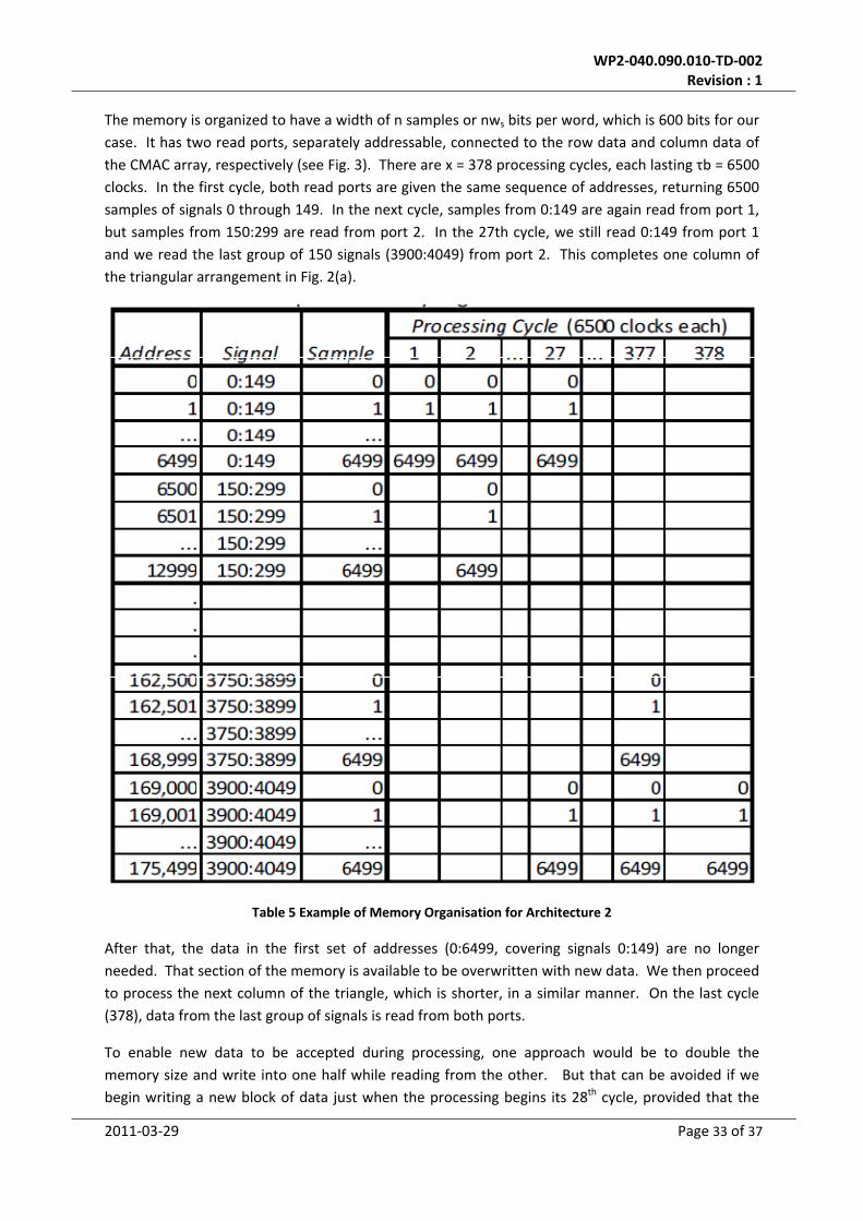
WP2‐040.090.010‐TD‐002 Revision : 1
2011‐03‐29 Page 33 of 37
The memory is organized to have a width of n samples or nws bits per word, which is 600 bits for our
case. It has two read ports, separately addressable, connected to the row data and column data of
the CMAC array, respectively (see Fig. 3). There are x = 378 processing cycles, each lasting τb = 6500
clocks. In the first cycle, both read ports are given the same sequence of addresses, returning 6500
samples of signals 0 through 149. In the next cycle, samples from 0:149 are again read from port 1,
but samples from 150:299 are read from port 2. In the 27th cycle, we still read 0:149 from port 1
and we read the last group of 150 signals (3900:4049) from port 2. This completes one column of
the triangular arrangement in Fig. 2(a).
Table 5 Example of Memory Organisation for Architecture 2
After that, the data in the first set of addresses (0:6499, covering signals 0:149) are no longer
needed. That section of the memory is available to be overwritten with new data. We then proceed
to process the next column of the triangle, which is shorter, in a similar manner. On the last cycle
(378), data from the last group of signals is read from both ports.
To enable new data to be accepted during processing, one approach would be to double the
memory size and write into one half while reading from the other. But that can be avoided if we
begin writing a new block of data just when the processing begins its 28th cycle, provided that the

WP2‐040.090.010‐TD‐002 Revision : 1
2011‐03‐29 Page 34 of 37
memory is organized as in Table 5. If the clock rate is such that the processing just keeps up with the
incoming data, then new data will never overwrite a buffer location until the old data in that location
has been processed, and new data will be available when needed for the next set of cycles.
10.3 ARCHITECTURE 3: MATRIX WITH RAM ACCUMULATORS
The overall structure of ICs for Architecture 3, shown in Figure 7, is similar to that for Architecture 2
(Fig. B1). The difference is that Architecture 3 processes a different set of n2 input
Figure 7 Overall structure of an IC for implementing Architecture 3.
samples on each clock, rather than processing the same set for bτ samples (one integration) before
proceeding to the next. This avoids the need for a large input buffer, but instead requires that each
CMAC have a bank of x accumulators implemented as a RAM, where x is the factor by which each
CMAC is shared among baselines. At the input, a small memory is still needed to hold a single
sample for each of the 2N signals.
Processing all baselines in each IC requires a sharing factor of x = (N/n)(2N/n+1) and n2 RAM
accumulators each of depth x. The total RAM is thus n2x = N(2N+n) words, which depends only
weakly on n. For our straw man design with N ≈ 2000, this amount of memory alone takes up more
than the 200 mm2 maximum die area. For example, at n2 = 2500 we need 2500 memories of x =
3240 32b words. These memories use 510 mm2 of die area in 90 nm CMOS. Therefore we cannot
process all baselines in each IC. By spreading the work across 8 ICs, we are able to find a design with
n = 102 (n2 = 10404 CMACs) where x = 100. The RAM accumulators for this case use 135 mm2, which
allows just enough room for the 10404 CMACs in the remaining 65 mm2. This is the design reported
in Table 2 and Table 3.
To fit the processing efficiently into 8 ICs per bandwidth segment, the arrangement of Figure 8 is
used. This enables all cross correlations of each IC to be useful, with no redundancy. A similar
arrangement is possible using c1 = 2k2 ICs for any positive integer k, leading to c1 = 2, 8, 18, 32, ...
Here c1=8 because this is the smallest value that supports N ≈ 2000 while keeping each IC smaller
than 200 mm2. (We could have accepted some inefficiency by using a triangular arrangement as we
did for Architectures 1 and 2, but in those cases there were hundreds of square matrices forming the
triangle, so the redundancy was a small fraction of the capacity. Here, if a 4x4 triangle of 10 ICs were
used, 4 halves of them would be redundant, which would be 20% of the capacity.)

WP2‐040.090.010‐TD‐002 Revision : 1
2011‐03‐29 Page 35 of 37
Figure 8 An arrangement of 8 ICs for correlating 2N signals. Each IC is capable of correlating N/2 signals
(entering from the left) against N/2 other signals (entering from the bottom). Unlabeled inputs in the
diagram receive the same signals as the IC to the left or below. The first four ICs (A, B, C, D) form a square
matrix that is split along the diagonal. The lower triangular part crosscorrelates all pairs of signals 1 through
N, and the upper triangular part cross‐correlates all pairs of signals N+1 through 2N. The other four ICs (E, F,
G, H) correlate signals 1 through N against signals N+1 through 2N. To accomplish this efficiently, it is
necessary for two of the ICs (A and D) to operate in a different mode from the others. These accept a total of
N signals (including N/2 signals entering from the top and from the right). Half of its CMACs are used to
correlate all pairs of the first N/2 signals, and the other half are used to correlate all pairs of the other N/2
signals. The self‐correlations (along the diagonal) require only half of a CMAC each, so they can be computed
for both sets of signals by using only N/2 CMACs. All 8 ICs can be identical, since they all need the same
resources and have the same number of inputs and outputs; A and D are made to operate differently by
asserting a mode control bit.
The resulting design is somewhat of a hybrid of Architectures 1 and 3, biased as far as possible
toward #3. Like #1, the clock rate is limited by the input data rate. We use 8 ICs per bandwidth
segment (vs. 284 ICs in #1), but we can process only 24 channels or 2.4 MHz of bandwidth (vs. 276
channels or 27.6 MHz) per segment. The net result is a reduction in the number of ICs by about a
factor of 3 compared with Architecture 1 and the same number as in Architecture 2. But the power
consumption is 2.6 times that of #1 and 2.2 times that of #2.
10.4 ARCHITECTURE 4: PIPELINE WITH DELAYS BETWEEN CMACS
Figure 9, taken from [5], is a more complete block diagram of a pipeline correlator structure than Fig.
2(b). It is drawn for the case of 352 input signals, and thus could be used for N = 176 dual‐
polarization antennas or for 352 single‐polarization antennas. The delays are appropriate for
integrations of bτ = 1024 samples.
The switches seen in Fig. B4 are a key feature to ensure that all CMACs are used efficiently. There
are N+1 CMACs and N switches. There are also N FIFO delays of length bτ, as well as one delay of
length Nbτ that drives the lower inputs of all switches. At the start of an integration, with data from
signal 1 entering the input, all switches are in the up position. After the first half of the signals (1

WP2‐040.090.010‐TD‐002 Revision : 1
2011‐03‐29 Page 36 of 37
through N) has been received at the input, all switches are moved to the down position while bτ
samples from signal N+1 are received. Then the right‐most switch is returned to the up position, and
after bτ samples are received from each of the following signals the next switch to the left is
returned to up. When the last sample from signal 2N is received, the last switch is returned to up
and we are back to the initial state,
Figure 9 Architecture 4 (pipeline with delays) block diagram, from [5].
ready for signal 1 again. For each set of bτ input samples, N+1 cross‐correlations are computed in
parallel and read out. By the end we have computed a total of 2N(N+1) = N(2N+2) correlations,
which is 1 more than th N(2N+1) needed, so one is redundant. This achieves a re‐use factor of x =
2N. Note that the re‐use factor is fixed by the architecture, unlike the matrix architectures where it
can be chosen by design.
In case the N+1 CMACs and associated delays are too large to fit in one IC, it is straightforward to
break the pipeline into as chain containing as many ICs as necessary. To do this, four streams of
samples must be passed between successive ICs, three in the forward direction (input, prompt, and
delayed) and one in the feedback direction (delayed). Thus a general purpose IC should be include
enough I/O capacity for these signals. For our straw man design in Architecture 4, it was just
possible to fit the CMACs and delay memories into one 200 mm2 IC for N=2000 (see Table 2).
In our model for the straw man design, each FIFO delay is implemented using a ws = 4 b wide by bτ =
6500 deep RAM. N=2000 of these are needed. The long (feedback) delay of length Nbτ is
implemented as N of the same RAMs in cascade, requiring 2N of them altogether. It might have
been slightly more efficient to make the long delay as a single RAM. However, we did simplify the
implementation by using 16b wide RAMs, so that 4 of the FIFOs are implemented in each RAM, and
so that only 2N/4 = N/2 of those 16b RAMs are needed. We could go further by using fewer RAMs
that are still wider, but the CACTI simulations showed that going to 32b width makes little difference
in die area but makes the cycle time longer. The clock rate, and hence the bandwidth (number of
channels K), at which our ASIC can run was limited by the RAM cycle time. K=1 (Kb = 100 kHz)
WP2‐040.090.010‐TD‐002 Revision : 1
2011‐03‐29 Page 37 of 37
requires a clock rate of 400 MHz, and the maximum is 695 MHz. With a different channel
bandwidth, it might have been possible to handle about 170 kHz per ASIC.
The model shows that this architecture uses 115 kW/beam for the straw man correlator, 4.5 times
that of #2, and requires 10,000 ICs, 3 times that of #2. These are consequences of the fact that the
power and die area are both dominated by the memories (83% and 94%, respectively, see Table 3).
10.5 . ARCHITECTURE 5: PIPLELINE WITH RAM ACCUMULATORS
As discussed in Section 4, this architecture has the same structure as #4 except that the delays
between CMACs are only for one sample, so they are implemented as registers that use negligible
energy and area. The feedback delay is of length N, so it might be implemented using a RAM, but
this RAM is small and there is only one of them, so it is neglected in our model. The CMACs are then
shared by providing each with a RAM accumulator.
We need N+1 = 2001 RAM accumulators, each of length 2N = 4000. But these need to store
wc = 32 b words (vs. the 4 b words of the delays in Architecture 4). The net result is that 256 Mb of
memory is needed (vs. 104 Mb in #4) to support the same number of CMACs, so the memory uses
an even fraction of the power and area (94% and 98% respectively). Therefore, this architecture is
by far the worst for power consumption (345 kW/beam) and IC count (30,000) in the straw man
system.
The larger memory area also means that N+1 CMACs cannot fit within the allowed 200 mm2 die
area. In our model, it was split among 3 identical ICs in cascade (see Section 10.4 for further
discussion).
As with Architecture 4, the bandwidth was limited to K=1 channel of b=100 kHz because larger
bandwidth would result in a clock rate that is too high for the memories.
Top Related