


Languages
Pages
Legal


MT9P031: 1/2.5-Inch 5-Mp Digital Image Sensor
Preliminary‡
MT9P031 Image SensorProduct Brief
Micron’s MT9P031 is a 1/2.5-inch CMOS digital image sensor
with an active-pixel array of 2592H x 1944V. It incorporates
sophisticated camera functions such as windowing, binning,
column and row skip mode, and snapshot mode. It is program-
mable through a simple two-wire serial interface. The MT9P031
produces extraordinarily clear, sharp digital pictures, and its ability
to capture both continuous video and single frames makes it the
perfect choice for a wide range of consumer and commercial secu-
rity applications, including high resolution network cameras; pan,
tilt, and zoom cameras; and hybrid video/still cameras.
Features• Micron® DigitalClarity®
imaging technology• High frame rate• Superior low-light
performance• Low dark current• Global reset release, which
starts the exposure of all rows simultaneously
• Bulb exposure mode, for arbitrary exposure times
• Snapshot mode to take frames on demand
• Horizontal and vertical mirror image
• Column and row skip modes to reduce image size without reducing field of view
• Column and row binning modes to improve image quality when resizing
• Simple two-wire serial interface
• Subframe windowed readout• Programmable controls: gain,
frame rate, frame size, exposure
• Automatic black level calibration
• On-chip PLL
Applications• High-resolution network
cameras• Wide field of view cameras• High-definition surveillance
camera• Dome cameras with electronic
pan, tilt, and zoom
• Hybrid video cameras with high resolution stills
• Detailed feature extraction for smart cameras
©2006 Micron Technology, Inc. All rights reserved.
‡Products and specifications discussed herein are for evaluation and reMicron without notice. Products are only warranted by Micron to m
Key ParametersOptical format 1/2.5-inch (4:3)Active imager size 5.70mm(H) x 4.28mm(V)
7.13mm diagonalActive pixels 2592H x 1944VPixel size 2.2µm x 2.2µmColor filter array RGB Bayer patternShutter type Global reset release (GRR),
snapshot only; electronic rolling shutter (ERS)
Maximum data rate/master clock
96 Mp/s at 96 MHz (2.8V I/O)48 Mp/s at 48MHz (1.8V I/O)
Frame RateFull resolution Programmable up to 14 fps VGA (with binning) Programmable up to 53 fps720P (1280 X 720, skipping mode)
Programmable up to 60 fps
ADC resolution 12-bit, on-chipResponsivity 1.4 V/lux-sec (550nm)Pixel dynamic range 70.1dB (full resolution),
76dB (2 x 2 binning)SNRMAX 38.1dB (full resolution),
44dB (2 x 2 binning)Supply voltage
I/O 1.7V−3.1VDigital 1.7V−1.9V (1.8V nominal)Analog 2.6V−3.1V (2.8V nominal)
Power consumption 381mW at 14 fps full resolution
Operating temp. –30°C to +70°C Packaging 48-pin iLCC, dieOutput gain 10 e-/LSBRead noise 2.6 e-RMS at 16XDark current 25 e-/pix/s at 55C
ference purposes only and are subject to change by eet Micron’s production data sheet specifications.

MT9P031: 1/2.5-Inch 5-Mp Digital Image SensorOrdering Information
Ordering Information
General DescriptionThe MT9P031 sensor can be operated in its default mode or programmed for frame size, exposure, gain setting, and other parameters. The default mode outputs a full-resolution image at 14 frames per second (fps).
An on-chip analog-to-digital converter (ADC) provides 12 bits per pixel. FRAME_VALID and LINE_VALID signals are output on dedicated pins, as is a pixel clock that is synchro-nous with valid data.
The 5-megapixel CMOS i`mage sensor features DigitalClarity—Micron’s breakthrough low-noise CMOS imaging technology that achieves CCD image quality (based on signal-to-noise ratio and low-light sensitivity) while maintaining the inherent size, cost, and integration advantages of CMOS.
Figure 1: MT9P031 Quantum Efficiency versus Wavelength
Table 1: Available Part Numbers
Part Number Description
MT9P031I12STC ES 48-Pin iLCC 7 degMT9P031I12STD ES Demo kitMT9P031I12STH ES Demo kit headboard
PDF: 09005aef824c993e/Source: 09005aef824c9943 Micron Technology, Inc., reserves the right to change products or specifications without notice.MT9P031_5100_PB_2.fm - Rev. B 8/07 EN 2 ©2006 Micron Technology, Inc. All rights reserved.

MT9P031: 1/2.5-Inch 5-Mp Digital Image SensorGeneral Description
Figure 2: Chief Ray Angle
CRA Design
0
2
4
6
8
10
12
14
0 10 20 30 40 50 60 70 80 90 100 110
Image Height (%)
CR
A (
deg
)
PDF: 09005aef824c993e/Source: 09005aef824c9943 Micron Technology, Inc., reserves the right to change products or specifications without notice.MT9P031_5100_PB_2.fm - Rev. B 8/07 EN 3 ©2006 Micron Technology, Inc. All rights reserved.
MT9P031: 1/2.5-Inch 5-Mp Digital Image SensorFunctional Overview
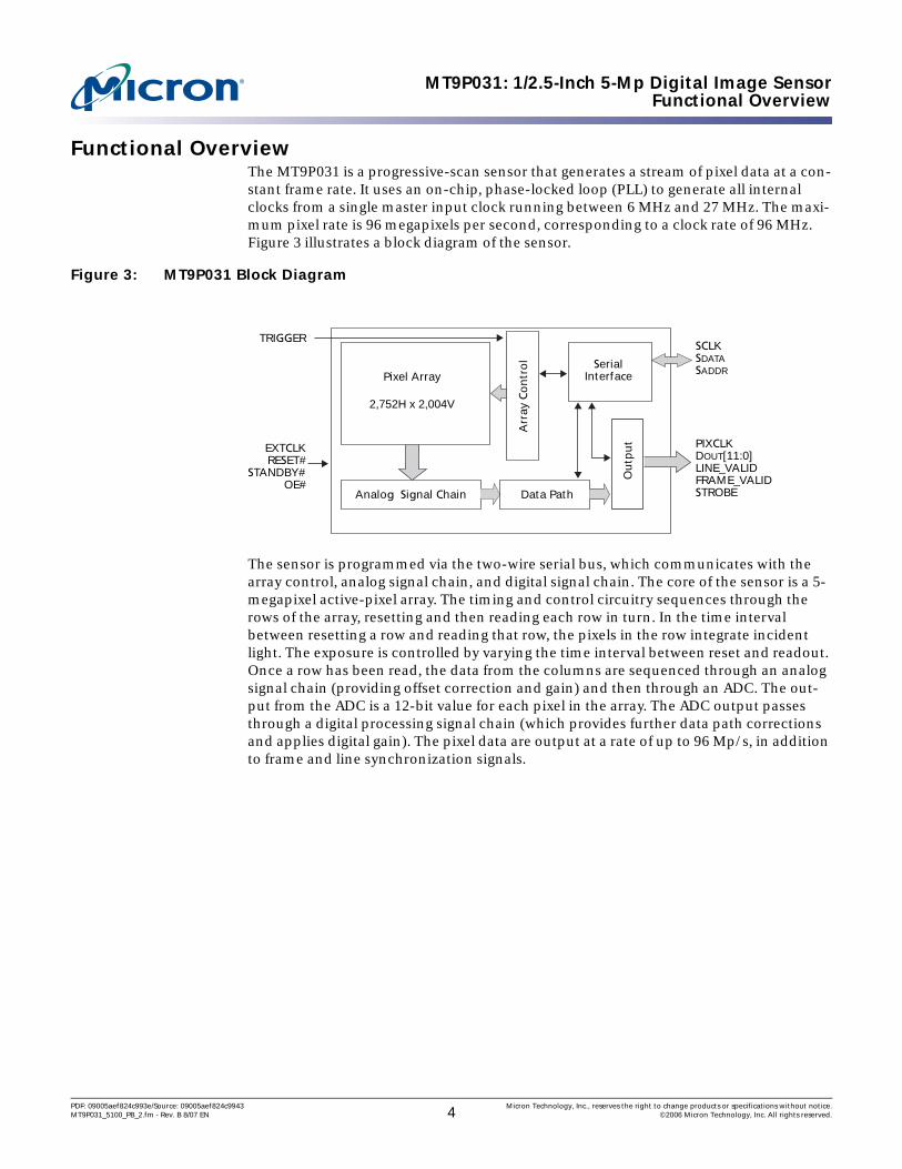
Functional OverviewThe MT9P031 is a progressive-scan sensor that generates a stream of pixel data at a con-stant frame rate. It uses an on-chip, phase-locked loop (PLL) to generate all internal clocks from a single master input clock running between 6 MHz and 27 MHz. The maxi-mum pixel rate is 96 megapixels per second, corresponding to a clock rate of 96 MHz. Figure 3 illustrates a block diagram of the sensor.
Figure 3: MT9P031 Block Diagram
The sensor is programmed via the two-wire serial bus, which communicates with the array control, analog signal chain, and digital signal chain. The core of the sensor is a 5-megapixel active-pixel array. The timing and control circuitry sequences through the rows of the array, resetting and then reading each row in turn. In the time interval between resetting a row and reading that row, the pixels in the row integrate incident light. The exposure is controlled by varying the time interval between reset and readout. Once a row has been read, the data from the columns are sequenced through an analog signal chain (providing offset correction and gain) and then through an ADC. The out-put from the ADC is a 12-bit value for each pixel in the array. The ADC output passes through a digital processing signal chain (which provides further data path corrections and applies digital gain). The pixel data are output at a rate of up to 96 Mp/s, in addition to frame and line synchronization signals.
Pixel Array
2,752H x 2,004V
SCLKSDATASADDR
PIXCLKDOUT[11:0]LINE_VALIDFRAME_VALIDSTROBE
SerialInterface
Analog Signal Chain Data Path
TRIGGER
EXTCLKRESET#
STANDBY#OE#
Arr
ay C
on
tro
l
Ou
tpu
t
PDF: 09005aef824c993e/Source: 09005aef824c9943 Micron Technology, Inc., reserves the right to change products or specifications without notice.MT9P031_5100_PB_2.fm - Rev. B 8/07 EN 4 ©2006 Micron Technology, Inc. All rights reserved.

MT9P031: 1/2.5-Inch 5-Mp Digital Image SensorFunctional Overview
Figure 4: Typical Configuration (connection)
Notes: 1. Resistor value 1.5KΩ is recommended but may be greater for slower two-wire speed.2. All power supplies should be adequately decoupled.3. All DGND pins must be tied together, as must all AGND pins, all VDDQ pins, and all VDD pins.
Figure 5: 48-Pin iLCC 10x10mm Package Pinout Diagram (top view)
DOUT[11:0]PIXCLK
FRAME_VALIDLINE_VALID
STROBE
SADDR
RESET#STANDBY#
SCLKSDATA
TRIGGER
VD
DQ
AG
ND
3
TEST
1.5K
Ω1
1.5K
Ω1
VDDQ2,3
VD
D
VDD2,3
1µF
10K
Ω
RSV
D
DG
ND
3
VD
DPL
LV
AA
PIX
VA
A
VAA2,3
OE#
ToControllerFrom
Controller
MasterClock
EXTCLK
123456 48 47 46 45 44 43
19 20 21 22 23 24 25 26 27 28 29 30
7
8
9
10
11
12
13
14
15
16
17
18
42
41
40
39
38
37
36
35
34
33
32
31
FRAME_VALID
LINE_VALID
STROBE
DGND
VDDQ
VDD
SADDR
STANDBY#
TRIGGER
RESET#
OE#
NC
DOUT8
DOUT7
DOUT6
VDDQ
DOUT5
DOUT4
DOUT3
DOUT2
DOUT1
DOUT0
PIXCLK
EXTCLK
NC
TEST
TEST
AG
ND
VA
A
VA
A
VD
DPL
L
DG
ND
NC
NC
NC
NC
RSV
D
SDA
TA
SCLK
TEST
AG
ND
VA
API
X V
AA
PIX
VD
D
DG
ND
DO
UT1
1
DO
UT1
0
DO
UT9
PDF: 09005aef824c993e/Source: 09005aef824c9943 Micron Technology, Inc., reserves the right to change products or specifications without notice.MT9P031_5100_PB_2.fm - Rev. B 8/07 EN 5 ©2006 Micron Technology, Inc. All rights reserved.
MT9P031: 1/2.5-Inch 5-Mp Digital Image SensorFunctional Overview
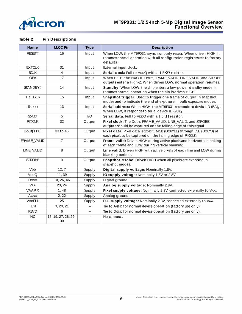
Table 2: Pin Descriptions
Name LLCC Pin Type Description
RESET# 16 Input When LOW, the MT9P031 asynchronously resets. When driven HIGH, it resumes normal operation with all configuration registers set to factory defaults.
EXTCLK 31 Input External input clock.SCLK 4 Input Serial clock: Pull to VDDQ with a 1.5KΩ resistor.OE# 17 Input When HIGH, the PIXCLK, DOUT, FRAME_VALID, LINE_VALID, and STROBE
outputs enter a High-Z. When driven LOW, normal operation resumes.STANDBY# 14 Input Standby: When LOW, the chip enters a low-power standby mode. It
resumes normal operation when the pin is driven HIGH.TRIGGER 15 Input Snapshot trigger: Used to trigger one frame of output in snapshot
modes and to indicate the end of exposure in bulb exposure modes.SADDR 13 Input Serial address: When HIGH, the MT9P031 responds to device ID (BA)H.
When LOW, it responds to serial device ID (90)H.SDATA 5 I/O Serial data: Pull to VDDQ with a 1.5KΩ resistor.
PIXCLK 32 Output Pixel clock: The DOUT, FRAME_VALID, LINE_VALID, and STROBE outputs should be captured on the falling edge of this signal.
DOUT[11:0] 33 to 45 Output Pixel data: Pixel data is 12-bit. MSB (DOUT11) through LSB (DOUT0) of each pixel, to be captured on the falling edge of PIXCLK.
FRAME_VALID 7 Output Frame valid: Driven HIGH during active pixels and horizontal blanking of each frame and LOW during vertical blanking.
LINE_VALID 8 Output Line valid: Driven HIGH with active pixels of each line and LOW during blanking periods.
STROBE 9 Output Snapshot strobe: Driven HIGH when all pixels are exposing in snapshot modes.
VDD 12, 7 Supply Digital supply voltage: Nominally 1.8V.VDDQ 11, 39 Supply IO supply voltage: Nominally 1.8V or 2.8V.DGND 10, 26, 46 Supply Digital ground.VAA 23, 24 Supply Analog supply voltage: Nominally 2.8V.
VAAPIX 1, 48 Supply Pixel supply voltage: Nominally 2.8V, connected externally to VAA.AGND 2, 22 Supply Analog ground.
VDDPLL 25 Supply PLL supply voltage: Nominally 2.8V, connected externally to VAA.TEST 3, 20, 21 – Tie to AGND for normal device operation (factory use only).RSVD 6 – Tie to DGND for normal device operation (factory use only).
NC 18, 19, 27, 28, 29, 30
– No connect.
PDF: 09005aef824c993e/Source: 09005aef824c9943 Micron Technology, Inc., reserves the right to change products or specifications without notice.MT9P031_5100_PB_2.fm - Rev. B 8/07 EN 6 ©2006 Micron Technology, Inc. All rights reserved.
MT9P031: 1/2.5-Inch 5-Mp Digital Image SensorFunctional Overview
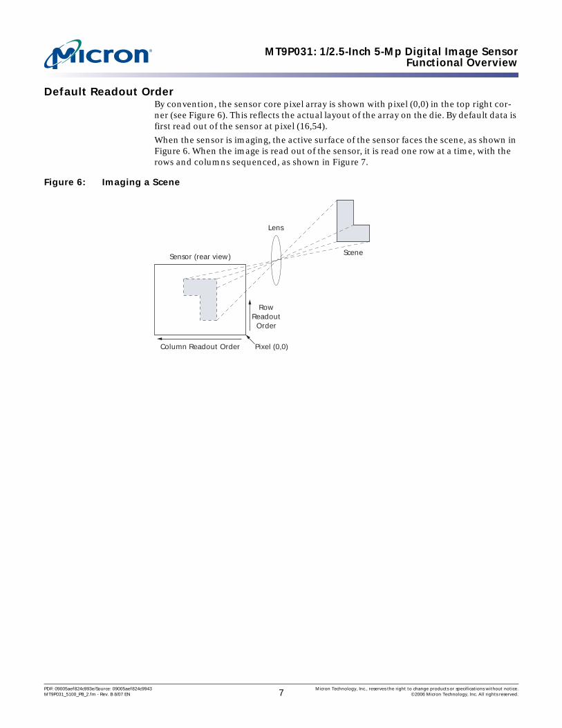
Default Readout OrderBy convention, the sensor core pixel array is shown with pixel (0,0) in the top right cor-ner (see Figure 6). This reflects the actual layout of the array on the die. By default data is first read out of the sensor at pixel (16,54).
When the sensor is imaging, the active surface of the sensor faces the scene, as shown in Figure 6. When the image is read out of the sensor, it is read one row at a time, with the rows and columns sequenced, as shown in Figure 7.
Figure 6: Imaging a Scene
Lens
Pixel (0,0)
RowReadout
Order
Column Readout Order
SceneSensor (rear view)
PDF: 09005aef824c993e/Source: 09005aef824c9943 Micron Technology, Inc., reserves the right to change products or specifications without notice.MT9P031_5100_PB_2.fm - Rev. B 8/07 EN 7 ©2006 Micron Technology, Inc. All rights reserved.

MT9P031: 1/2.5-Inch 5-Mp Digital Image SensorFunctional Overview
Output Data Format (default mode)The MT9P031 image data is read out in a progressive scan. Valid image data is sur-rounded by horizontal blanking and vertical blanking, as shown in Figure 7. LINE_VALID is HIGH in the shaded region of the figure.
Figure 7: Spatial Illustration of Image Readout
P0,0 P0,1 P0,2.....................................P0,n-1 P0,nP1,0 P1,1 P1,2.....................................P1,n-1 P1,n
00 00 00 .................. 00 00 0000 00 00 .................. 00 00 00
Pm-1,0 Pm-1,1.....................................Pm-1,n-1 Pm-1,nPm,0 Pm,1.....................................Pm,n-1 Pm,n
00 00 00 .................. 00 00 0000 00 00 .................. 00 00 00
00 00 00 .................. 00 00 0000 00 00 .................. 00 00 00
00 00 00 .................. 00 00 0000 00 00 .................. 00 00 00
00 00 00 ..................................... 00 00 0000 00 00 ..................................... 00 00 00
00 00 00 ..................................... 00 00 0000 00 00 ..................................... 00 00 00
VALID IMAGE HORIZONTALBLANKING
VERTICAL BLANKING VERTICAL/HORIZONTALBLANKING
PDF: 09005aef824c993e/Source: 09005aef824c9943 Micron Technology, Inc., reserves the right to change products or specifications without notice.MT9P031_5100_PB_2.fm - Rev. B 8/07 EN 8 ©2006 Micron Technology, Inc. All rights reserved.

MT9P031: 1/2.5-Inch 5-Mp Digital Image SensorFunctional Overview
Readout Modes
SubsamplingBy default, the resolution of the output image is the full width and height of the FOV as defined above. The output resolution can be reduced by two methods: skipping and bin-ning.
Row and column skip modes use subsampling to reduce the output resolution without reducing field-of-view. The MT9P031 also has row and column binning modes, which can reduce the impact of aliasing introduced by the use of skip modes. This is achieved by the averaging of two or three adjacent rows and columns (adjacent same-color pix-els). Both 2X and 4X binning modes are supported. Rows and columns can be binned independently.
SkippingSkipping reduces resolution by using only selected pixels from the FOV in the output image. In skip mode, entire rows and columns of pixels are not sampled, resulting in a lower-resolution output image. A skip 2X mode skips one Bayer pair of pixels for every pair output. Skip 3X skips two pairs for each one pair output. Rows and columns are always read out in pairs.
Binning Binning reduces resolution by combining adjacent, same-color imager pixels to produce one output pixel. All of the pixels in the FOV contribute to the output image in bin mode. This can result in a more pleasing output image with reduced subsampling artifacts. It also improves low-light performance. For columns, the combination step can be either an averaging or summing operation. Depending on lighting conditions, one or the other may be desirable. In low-light conditions, summing produces a gain roughly equivalent to the column bin factor.
Only certain combinations of binning and skipping are allowed.
PDF: 09005aef824c993e/Source: 09005aef824c9943 Micron Technology, Inc., reserves the right to change products or specifications without notice.MT9P031_5100_PB_2.fm - Rev. B 8/07 EN 9 ©2006 Micron Technology, Inc. All rights reserved.

MT9P031: 1/2.5-Inch 5-Mp Digital Image SensorDC Electrical Characteristics
DC Electrical Characteristics
Table 3: DC Electrical Characteristics
Symbol Definition Conditions Min Typ Max Units
VDD Core digital voltage 1.7 1.8 1.9 V
VDDQ I/O digital voltage 1.7 1.8/2.8 3.1 V
VAA Analog voltage 2.6 2.8 3.1 V
VAAPIX Pixel supply voltage 2.6 2.8 3.1 V
VDDPLL PLL supply voltage 2.6 2.8 3.1 V
VIH Input high voltage VDDQ = 2.8VVDDQ = 1.8V
21.3
– 3.32.3
V
VIL Input low voltage VDDQ = 2.8VVDDQ = 1.8V
–0.3–0.3
– +0.8+0.5
V
IIN Input leakage current No pull-up resistor; VIN = VDDQ or DGND
– <10 – µA
VOH Output high voltage At specified IOH 1.3 – 1.82 V
VOL Output low voltage At specified IOL 0.16 – 0.35 V
IOH Output high current At specified VOH = VDDQ-400mv at 1.7V VDDQ
8.9 – 22.3 mA
IOL Output low current At specified VOL = 400mv at 1.7V VDDQ
2.6 – 5.1 mA
IOZ Tri-state output leakage current VIN=VDDQ or GND – – 2 µA
IDD1 Digital operating current Parallel mode 96 MHz full frame nominal voltage, PLL enabled
– 28 35 mA
IDDQ1 I/O digital operating current Parallel mode 96 MHz full frame nominal voltage, PLL enabled
– 38.6 50 mA
IAA1 Analog operating current Parallel mode 96 MHz full frame nominal voltage, PLL enabled
– 72 95 mA
IAAPIX1 Pixel supply current Parallel mode 96 MHz full frame nominal voltage, PLL enabled
– 2.4 6 mA
IDDPLL1 PLL supply current Parallel mode 96 MHz full frame nominal voltage, PLL enabled
– 5 6 mA
IDD2 Digital operating current Parallel mode 96 MHz 4X binning nominal voltage, PLL enabled
– 15 35 mA
IDDQ2 I/O digital operating current Parallel mode 96 MHz 4X binning nominal voltage, PLL enabled
– 6.4 50 mA
IAA2 Analog operating current Parallel mode 96 MHz 4X binning nominal voltage, PLL enabled
– 69 95 mA
IAAPIX2 Pixel supply current Parallel mode 96 MHz 4X binning nominal voltage, PLL Enabled
– 3.4 6 mA
IDDPLL2 PLL supply current Parallel mode 96 MHz 4X binning nominal voltage, PLL enabled
– 5 6 mA
ISTBY1 Hard standby current PLL enabled
EXTCLK enabled – <500 – µA
ISTBY2 Hard standby current PLL disabled
EXTCLK disabled – <50 – µA
ISTBY3 Soft standby current PLL enabled EXTCLK enabled (PLL enabled) – <500 – µA
ISTBY4 Soft standby current PLL disabled
EXTCLK enabled (PLL disabled) – <500 – µA
PDF: 09005aef824c993e/Source: 09005aef824c9943 Micron Technology, Inc., reserves the right to change products or specifications without notice.MT9P031_5100_PB_2.fm - Rev. B 8/07 EN 10 ©2006 Micron Technology, Inc. All rights reserved.

MT9P031: 1/2.5-Inch 5-Mp Digital Image SensorDC Electrical Characteristics
Notes: 1. Stresses greater than those listed may cause permanent damage to the device. This is a stress rating only, and functional operation of the device at these or any other conditions above those indicated in the operational sections of this specification is not implied. Expo-sure to absolute maximum rating conditions for extended periods may affect reliability.
2. In order to keep dark current and shot noise artifacts from impacting image quality, care should be taken to keep TOP at a minimum.
3. Measure at junction.
Table 4: Power Consumption
Mode Full Resolution (14 fps) 4X Binning Units
Streaming 381 262 mW
Table 5: Absolute Maximum Ratings
Symbol Definition Min Max Units
VDD_MAX Core digital voltage –0.3 1.9 V
VDDQ_MAX I/O digital voltage –0.3 3.1 V
VAA_MAX Analog voltage –0.3 3.1 V
VAAPIX_MAX Pixel supply voltage –0.3 3.1 V
VDDPLL_MAX PLL supply voltage –0.3 3.1 V
VIN_MAX Input voltage –0.3 VDDQ + 0.3 V
IDD_MAX Digital operating current – 35 mA
IDDQ_MAX I/O digital operating current – 100 mA
IAA_MAX Analog operating current – 95 mA
IAAPIX_MAX Pixel supply current – 6 mA
IDDPLL_MAX PLL supply current – 6 mA
TOP 2, 3 Operating temperature –30 70 °C
TST Storage temperature –40 125 °C
PDF: 09005aef824c993e/Source: 09005aef824c9943 Micron Technology, Inc., reserves the right to change products or specifications without notice.MT9P031_5100_PB_2.fm - Rev. B 8/07 EN 11 ©2006 Micron Technology, Inc. All rights reserved.

MT9P031: 1/2.5-Inch 5-Mp Digital Image SensorPackage Dimensions
Package Dimensions
Figure 8: 48-Pin iLCC Package Outline
Notes: 1. All dimensions are in millimeters.
4.50
10.000 ±0.075
3.85
7.70
3.85
0.70TYP
0.70TYP
7.70
48 1
1.4047X 0.80
48X 0.40
4.50
10.000 ±0.075
7.571.455
5.702CTR
7.024.277CTR
1.45
C L
C LLEAD FINISH: GOLD PLATING,0.50 MICRONSMINIMUM THICKNESS
4.20
5.000 ±0.075OPTICAL CENTER
CB
OPTICALAREA
MAXIMUM ROTATION OF OPTICAL AREA RELATIVE TO PACKAGE EDGES B AND C : 1ºMAXIMUM TILT OF OPTICAL AREA RELATIVE TO SEATING PLANE A : 25 MICRONS RELATIVE TO TOP OF COVER GLASS D : 50 MICRONS
5.000 ±0.075OPTICAL CENTER
FIRSTCLEARPIXEL
SEATINGPLANE
MOLD COMPOUND: EPOXY NOVOLAC
IMAGE SENSOR DIELID MATERIAL: BOROSILICATE GLASS 0.40 THICKNESS
1.250 ±0.125
0.725 ±0.075
0.525 ±0.050
0.125 (FOR REFERENCE ONLY)
SUBSTRATE MATERIAL: PLASTIC LAMINATE
A
D
®
8000 S. Federal Way, P.O. Box 6, Boise, ID 83707-0006, Tel: [email protected] www.micron.com Customer Comment Line: 800-932-4992
Micron, the M logo, and the Micron logo are trademarks of Micron Technology, Inc. All other trademarks are the property of their respective owners.
PDF: 09005aef824c993e/Source: 09005aef824c9943 Micron Technology, Inc., reserves the right to change products or specifications without notice.MT9P031_5100_PB_2.fm - Rev. B 8/07 EN 12 ©2006 Micron Technology, Inc. All rights reserved.
Top Related