
![WORLD ANTI-DOPING AGENCY and THE ANTI-DOPING ORGANIZATION · world anti-doping agency and the anti-doping organization [insert name] _____ agreement governing the use and sharing](https://static.fdocuments.us/doc/165x107/5c1bae9309d3f2826b8b8c64/world-anti-doping-agency-and-the-anti-doping-organization-world-anti-doping.jpg)


Languages
Pages
Legal

Lecture 5.0Lecture 5.0
Properties of Semiconductors
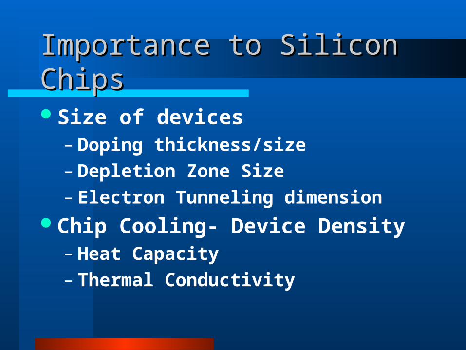
Importance to Silicon ChipsImportance to Silicon Chips
Size of devices– Doping thickness/size– Depletion Zone Size– Electron Tunneling dimension
Chip Cooling- Device Density– Heat Capacity– Thermal Conductivity
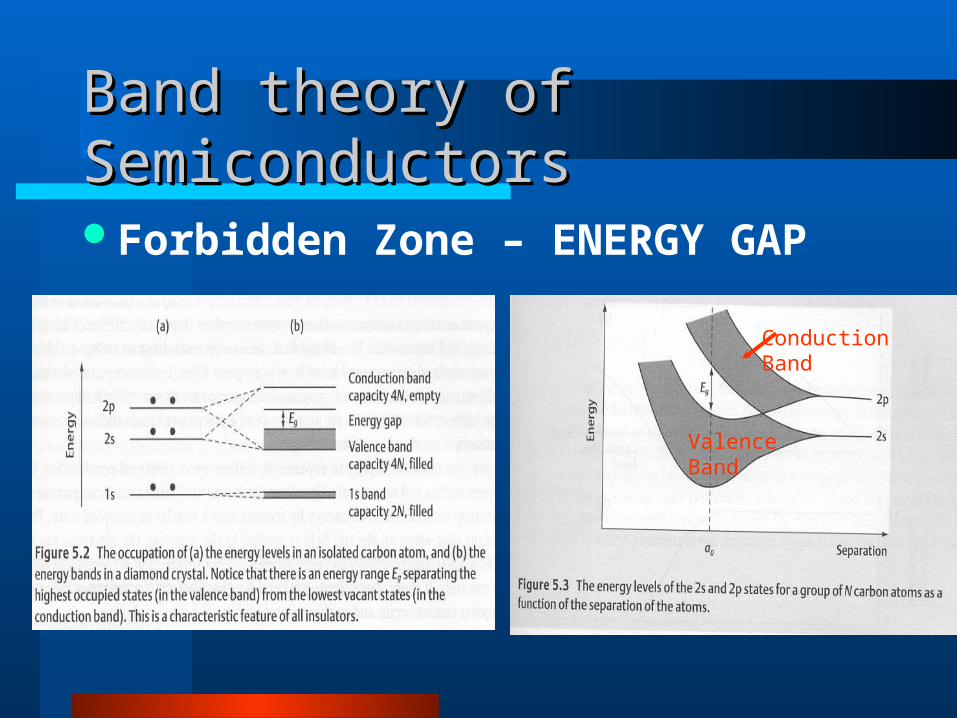
Band theory of SemiconductorsBand theory of Semiconductors
Forbidden Zone – ENERGY GAP
ValenceBand
ConductionBand
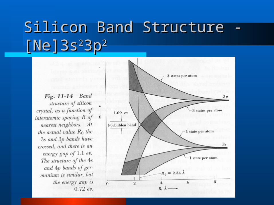
Silicon Band Structure - [Ne]3sSilicon Band Structure - [Ne]3s223p3p22
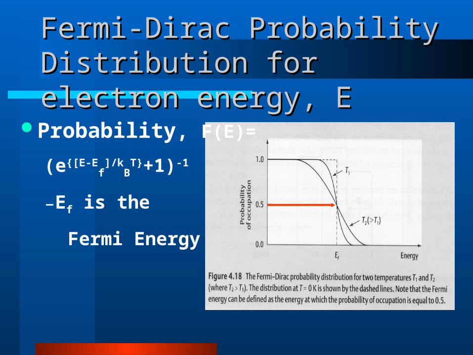
Fermi-Dirac Probability Fermi-Dirac Probability Distribution for electron energy, EDistribution for electron energy, E
Probability, F(E)=
(e{[E-Ef]/k
BT}+1)-1
–Ef is the
Fermi Energy
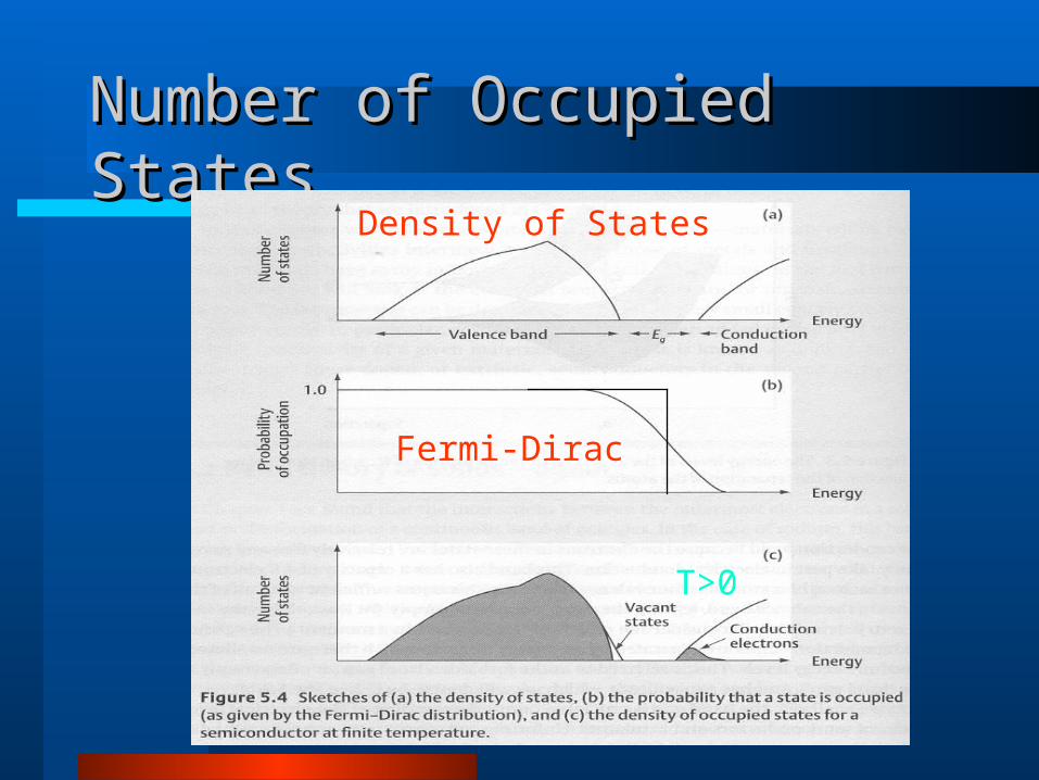
Number of Occupied StatesNumber of Occupied States
Fermi-Dirac
Density of States
T>0
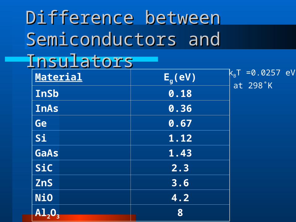
Difference between Difference between Semiconductors and InsulatorsSemiconductors and Insulators
Material Eg(eV)
InSb 0.18
InAs 0.36
Ge 0.67
Si 1.12
GaAs 1.43
SiC 2.3
ZnS 3.6
NiO 4.2
Al2O3 8
kBT =0.0257 eV
at 298˚K

Probability of electrons in Probability of electrons in Conduction BandConduction Band
Lowest Energy in CBE-Ef Eg/2
Probability in CBF(E)= (exp{[E-Ef]/kBT} +1)-1 )
= (exp{Eg/2kBT} +1)-1
exp{-Eg/2kBT} for Eg>1 eV @ 298K
kBT =0.0257 eV
at 298˚K
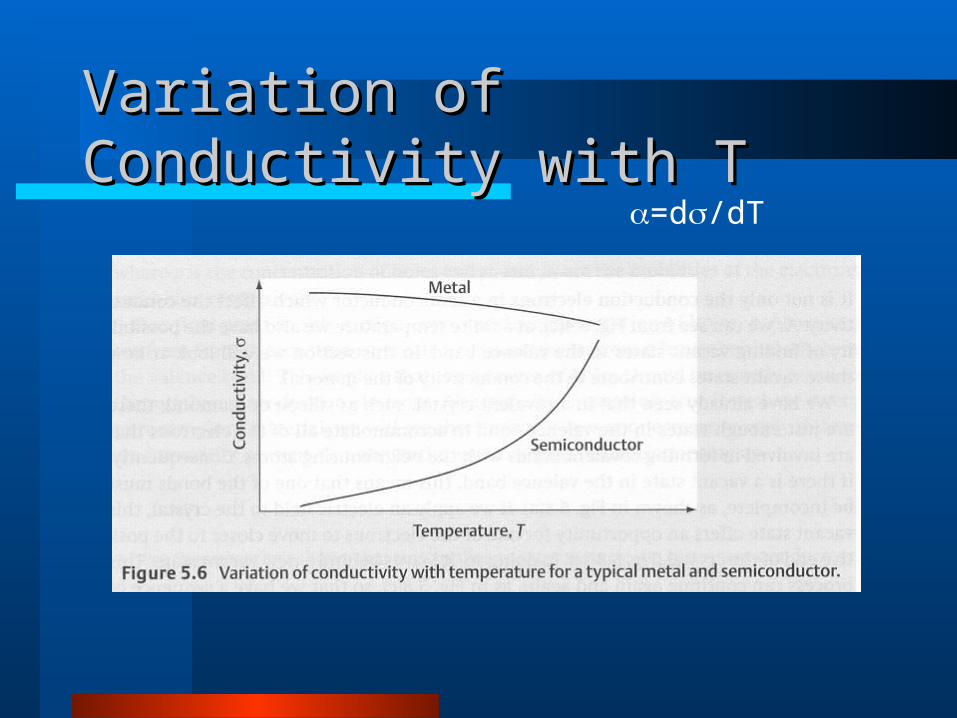
Variation of Conductivity with TVariation of Conductivity with T=d/dT
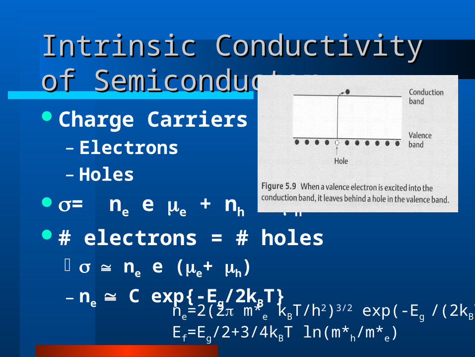
Intrinsic Conductivity of Intrinsic Conductivity of SemiconductorSemiconductorCharge Carriers – Electrons– Holes
= ne e e + nh e h
# electrons = # holes ne e (e+ h)
– ne C exp{-Eg/2kBT} ne=2(2 m*e kBT/h2)3/2 exp(-Eg /(2kBT))Ef=Eg/2+3/4kBT ln(m*h/m*e)
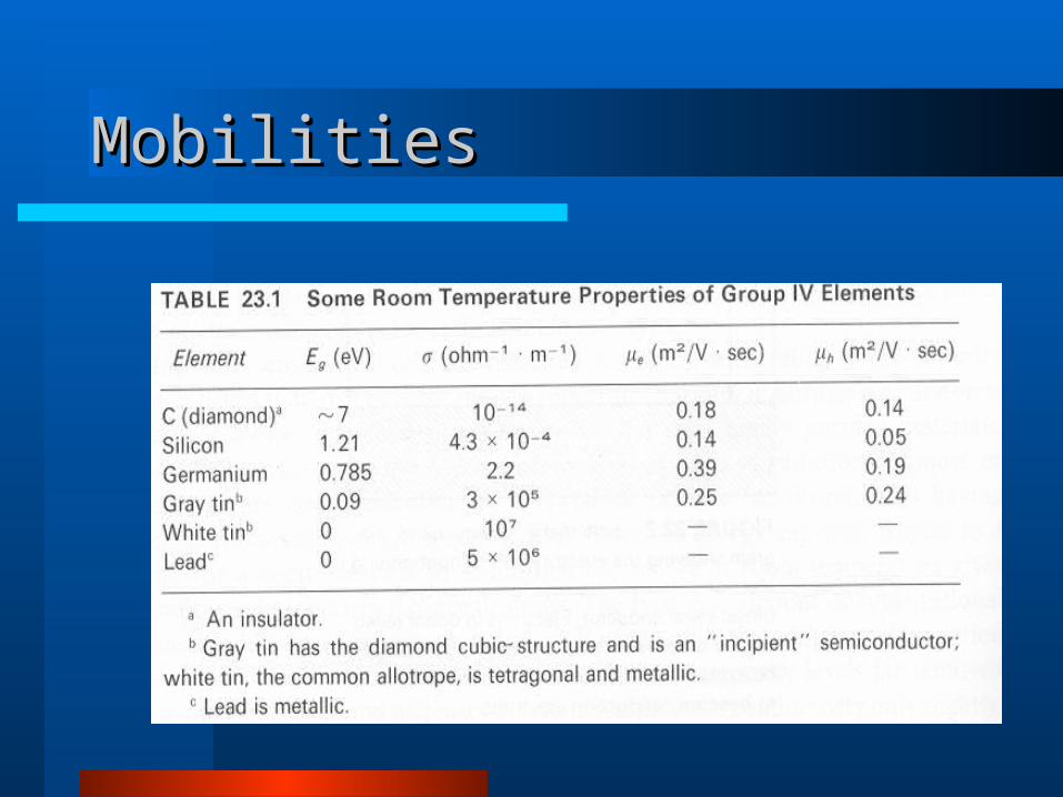
MobilitiesMobilities
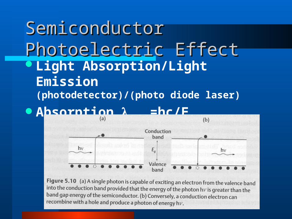
Semiconductor Photoelectric EffectSemiconductor Photoelectric EffectLight Absorption/Light Emission
(photodetector)/(photo diode laser)
Absorption max =hc/Eg
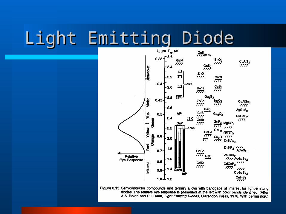
Light Emitting DiodeLight Emitting Diode
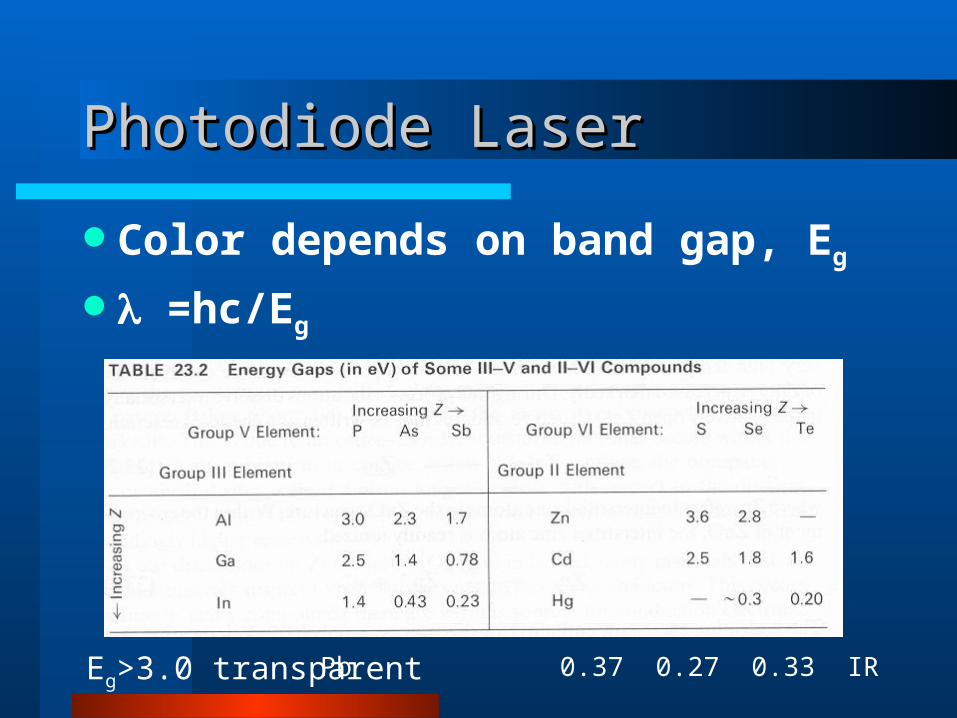
Photodiode LaserPhotodiode Laser
Color depends on band gap, Eg
=hc/Eg
Pb 0.37 0.27 0.33 IR detectors
Eg>3.0 transparent
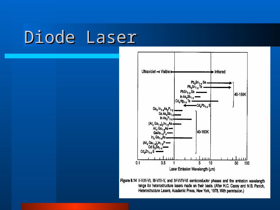
Diode LaserDiode Laser

Extrinsic Conductivity of SemiconductorExtrinsic Conductivity of Semiconductor
Donor Doping Acceptor Dopingn-type p-type
p= 2(2 m*h kBT/h2)3/2 exp(-Ef/kBT)
Law of Mass Action, Nipi=ndpd or =nndn
N=nd+ni

Extrinsic Conductivity of SemiconductorExtrinsic Conductivity of Semiconductor
Donor Doping Acceptor Doping

Electron DensityElectron Density
Dopant Concentration effects Electron
DensityElectrical
Conductivity

ConductivityConductivity
Intrinsic Range– Exponential with T
Extrinsic Range– Promoted to CB
– Decreasing , – Joins Intrinsic
Majority/minority Carriers
= ne e e + nh e h
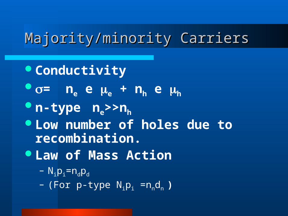
Majority/minority CarriersMajority/minority Carriers
Conductivity= ne e e + nh e h
n-type ne>>nh Low number of holes due to
recombination.Law of Mass Action
– Nipi=ndpd – (For p-type Nipi =nndn )

Extrinsic Conductivity of SemiconductorExtrinsic Conductivity of Semiconductor
Donor Doping Acceptor Dopingn-type p-type
Ed = -m*e e4/(8 (o)2 h2)Ef=Eg-Ed/2 Ef=Eg+Ea/2

Effective MassEffective Mass
HolesElectrons
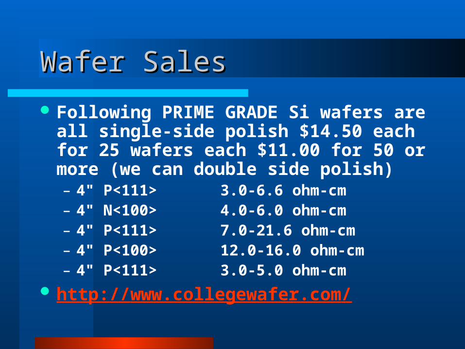
Wafer SalesWafer Sales
Following PRIME GRADE Si wafers are all single-side polish $14.50 each for 25 wafers each $11.00 for 50 or more (we can double side polish)– 4" P<111> 3.0-6.6 ohm-cm– 4" N<100> 4.0-6.0 ohm-cm– 4" P<111> 7.0-21.6 ohm-cm– 4" P<100> 12.0-16.0 ohm-cm– 4" P<111> 3.0-5.0 ohm-cm
http://www.collegewafer.com/
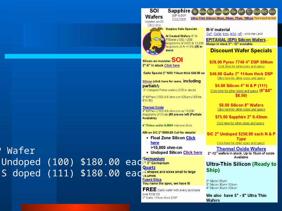
GaP Wafer2" Undoped (100) $180.00 each 2" S doped (111) $180.00 each
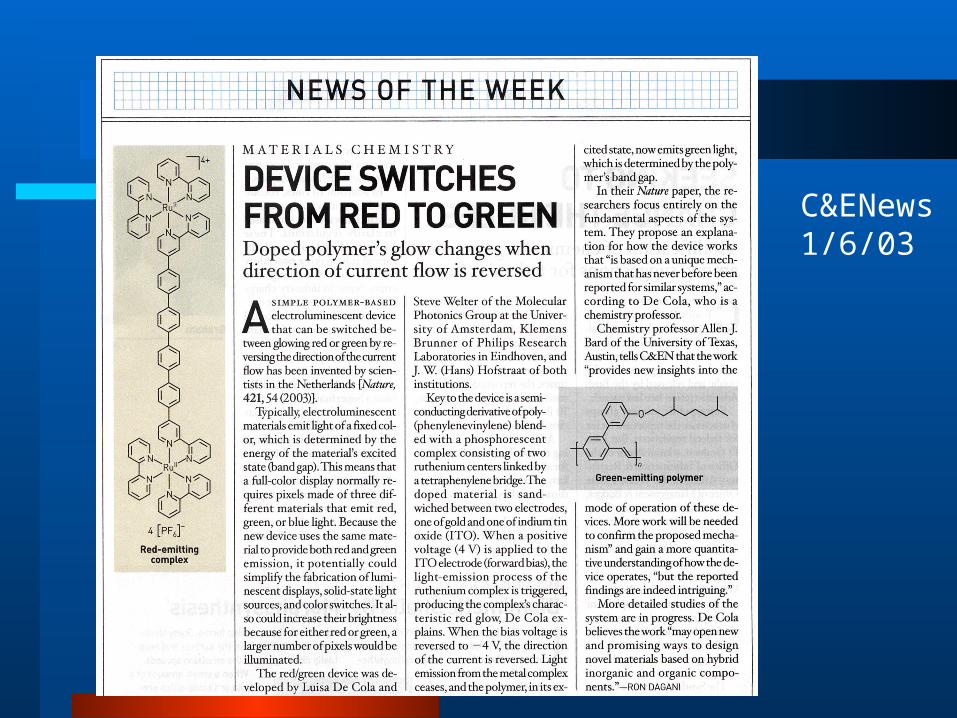
C&ENews1/6/03
Top Related