


Languages
Pages
Legal

EECE 407 Microprocessor and Interfacing
Level – 4/Term – II30 June, 2013 – 01 December 2013
Course Teacher
Shuvro Chowdhury
Lecturer
Department of Electrical and Electronic Engineering
Bangladesh University of Engineering and Technology
http://teacher.buet.ac.bd/schowdhury

About the Course
• 3 credits, 3 hours/week
• Scheduled class time
• Wednesday at 8.00 A.M. – 10.50 A.M.
• Class duration is 3 hours.
EECE 407 Microprocessor and Interfacing Shuvro Chowdhury, Lecturer, Dept. of EEE, BUET 2

Course Outline
Introduction to microprocessors.
Intel 8086 microprocessor: Architecture, addressing modes,
instruction sets, assembly language programming, system design
and interrupt.
Interfacing: Programmable peripheral interface, programmable
timer, serial communication interface, programmable interrupt
controller, direct memory access, keyboard and display interface.
Introduction to micro-controllers.
EECE 407 Microprocessor and Interfacing Shuvro Chowdhury, Lecturer, Dept. of EEE, BUET 3

Marks Distribution
EECE 407 Microprocessor and Interfacing Shuvro Chowdhury, Lecturer, Dept. of EEE, BUET 4
Category Total
marks
Percentage
(%)
Attendance 30 10
Class test
(best 3 will
be counted)
4 20 × 3 = 60 20
Term final
exam
1 210 70
Total 300 100

Grade Distribution
EECE 407 Microprocessor and Interfacing Shuvro Chowdhury, Lecturer, Dept. of EEE, BUET 5
Marks (%) Grade Point Letter Grade
80 - 100 4.00 A+
75 - 79 3.75 A
70 - 74 3.50 A-
65 - 69 3.25 B+
60 - 64 3.00 B
55 - 59 2.75 B-
50 - 54 2.50 C+
45 - 49 2.25 C
40 - 44 2.00 D
< 40 0.00 F

Reference Books
Text Books:
1. Digital Computer Electronics –Albert P. Malvino and Jerald A. Brown (3rd Edition)
2. Assembly Language Programming and Organization of the IBM PC – Ytha Yu and
Charles Marut
3. Microprocessor and Interfacing Programming and Hardware – Douglas V. Hall
Reference Books:
1. Microprocessors and Microcomputer-Based System Design– Mohammed
Rafiquzzaman (2nd edition)
2. The Intel Microprocessors – Barry B. Brey (6th Edition)
3. The 8051 Microcontroller and Embedded Systems – M. A. Mazidi, J. G. Mazidi, R.
D. McKinlay
EECE 407 Microprocessor and Interfacing Shuvro Chowdhury, Lecturer, Dept. of EEE, BUET 6

For Further Contact
Shuvro ChowdhuryLecturerDepartment of Electrical and Electronic EngineeringBangladesh University of Engineering and TechnologyDhaka-1000, Bangladesh.
Room No.: 431 (Fourth Floor), ECE BuildingWest Palashi, Dhaka, Bangladesh.
Mobile: +880 1717 225412E-mail: [email protected], [email protected]
EECE 407 Microprocessor and Interfacing Shuvro Chowdhury, Lecturer, Dept. of EEE, BUET 7

Components of a Computer System

Central Processing Unit (CPU)
Basic Elements of a Computer System
EECE 407 Microprocessor and Interfacing Shuvro Chowdhury, Lecturer, Dept. of EEE, BUET 9
Memory
Arithmetic Logic Unit (ALU)
Control Unit
InputDevices
OutputDevices
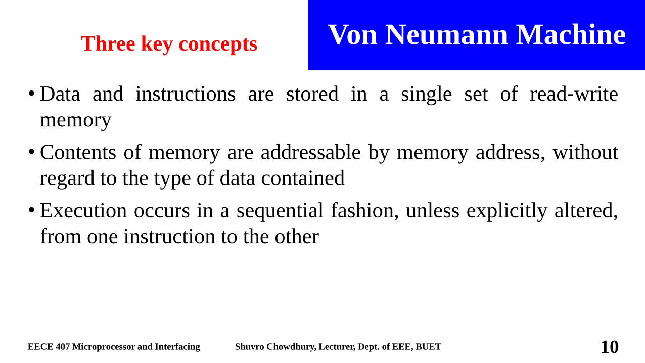
Von Neumann Machine
• Data and instructions are stored in a single set of read‐write
memory
• Contents of memory are addressable by memory address, without
regard to the type of data contained
• Execution occurs in a sequential fashion, unless explicitly altered,
from one instruction to the other
EECE 407 Microprocessor and Interfacing Shuvro Chowdhury, Lecturer, Dept. of EEE, BUET 10
Three key concepts

Computer System Components
• Memory
• Stores instructions and data
• Input/Output
• Called peripherals
• Used to input and output instructions and data
• Arithmetic and Logic Unit
• Performs arithmetic operations (addition, subtraction)
• Performs logical operations (AND, OR, XOR, SHIFT,ROTATE)
EECE 407 Microprocessor and Interfacing Shuvro Chowdhury, Lecturer, Dept. of EEE, BUET 11

Computer System Components
• Control Unit
• Coordinates the operation of the computer
• System Interconnection and Interaction
• Bus — A group of lines used to transfer bits between the microprocessorand other components of the computer system. Bus is used to communicatebetween parts of the computer. There is only one transmitter at a time andonly the addressed device can respond.
• Types
• Address
• Data
• Control signals
EECE 407 Microprocessor and Interfacing Shuvro Chowdhury, Lecturer, Dept. of EEE, BUET 12

Microprocessor
A silicon chip that contains a CPU. In the world of personal
computers, the terms microprocessor and CPU are used
interchangeably. At the heart of all personal computers and most
workstations sits a microprocessor. Microprocessors also control the
logic of almost all digital devices, from clock radios to fuel-
injection systems for automobiles.
EECE 407 Microprocessor and Interfacing Shuvro Chowdhury, Lecturer, Dept. of EEE, BUET 13

Microprocessor
• is a semiconductor device consisting of electronic logic circuits
• manufactured by using various fabrication schemes
• capable of performing computing functions
• capable of transporting data/information
• is a programmable device
• the programmer selects instruction from the list and determines the sequence
of execution for a given task.
• can be divided into 3 segments:
• Arithmetic and Logic Unit
• Register Unit
• Control Unit
EECE 407 Microprocessor and Interfacing Shuvro Chowdhury, Lecturer, Dept. of EEE, BUET 14

Differentiating Characters of Microprocessors
• Instruction set: The set of instructions that the microprocessor
can execute.
• Bandwidth : The number of bits processed in a single instruction.
• Clock speed : Given in megahertz (GHz), the clock speed
determines how many instructions per second the processor can
execute.
EECE 407 Microprocessor and Interfacing Shuvro Chowdhury, Lecturer, Dept. of EEE, BUET 15

CPU Components
• Generates control signals which are necessary for execution of aninstruction.
• Connect registers to the bus.
• Controls the data flow between CPU and peripherals (includingmemory).
• Provides status, control & timing signals required for the operation ofmemory and I/O devices to the system.
• Acts as a brain of computer system
• All actions of the control unit are associated with the decoding andexecutions of instructions (fetch and execute cycles).
EECE 407 Microprocessor and Interfacing Shuvro Chowdhury, Lecturer, Dept. of EEE, BUET 16
Control Unit

CPU Components
• Hold data, instructions, or other items
• Various sizes
• Program counter and memory address registers must be of same
size/width as address bus
• Registers which hold data must be of same size/width as memory
words
EECE 407 Microprocessor and Interfacing Shuvro Chowdhury, Lecturer, Dept. of EEE, BUET 17
Registers
CPU Components
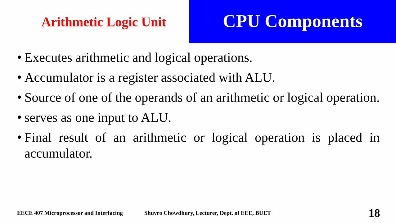
• Executes arithmetic and logical operations.
• Accumulator is a register associated with ALU.
• Source of one of the operands of an arithmetic or logical operation.
• serves as one input to ALU.
• Final result of an arithmetic or logical operation is placed in
accumulator.
EECE 407 Microprocessor and Interfacing Shuvro Chowdhury, Lecturer, Dept. of EEE, BUET 18
Arithmetic Logic Unit

Arithmetic and Logic Unit
ALU performs the following arithmetic & logical operations:
• Addition
• Subtraction
• Logical AND
• Logical OR
• Logical EXCLUSIVE OR
• Complement(logical NOT)
• Increment (add 1)
• Decrement (subtract 1)
• Left shift, Rotate Left, Rotate right
• Clear etc.
EECE 407 Microprocessor and Interfacing Shuvro Chowdhury, Lecturer, Dept. of EEE, BUET 19
Functions

Simple As Possible ComputerVersion 1(SAP - 1 )

SAP – 1
• Designed for the beginners.
• Main purpose is to introduce all the crucial ideas behind computer
operation avoiding too much details.
• There are three generations of SAP. SAP-1 is the first stage
towards the evolution of modern computers.
We shall try to cover SAP-1 and SAP-2 if time permits
EECE 407 Microprocessor and Interfacing Shuvro Chowdhury, Lecturer, Dept. of EEE, BUET 21
Introduction

SAP – 1
EECE 407 Microprocessor and Interfacing Shuvro Chowdhury, Lecturer, Dept. of EEE, BUET 22
Architecture
Program
Counter
Input and
MAR
16 x 8 RAM
Instruction
Register
Accumulator
Adder/
Subtractor
B
Register
Controller/
Sequencer
Output
Register
8
4
8
Binary
Display
4
8
4
12
8
8
CLKCLR
CPEP
LM
CLK
CE
LI
CLK
LACLKEA
SU
EU
LB
CLK
LO
CLK
CON = CPEPLMCELIEILAEASUEULBLO
CLR
CLKCLRCLKCLR
W BUS
8
4
4
4
EI
8
8
8
8

SAP – 1
• Bus organized architecture.
• All register outputs to the W-bus are three state which allows
orderly transfer of data.
• All other register outputs are two-state.
EECE 407 Microprocessor and Interfacing Shuvro Chowdhury, Lecturer, Dept. of EEE, BUET 23
Architecture

SAP – 1 Architecture
• A part of control unit.
• 4-bit up counter, counts from 0000 to 1111.
• The program for the computer is stored at the beginning of the memory with thefirst instruction at binary address 0000.
• Its job is to send to the memory address of the next instruction to be fetched andexecuted.
• Program counter is reset to 0000 before each computer run.
• At the beginning it sends address 0000 to memory.
• Then the counter is incremented to 0001.
• When the first instruction is fetched and executed, it sends address 0001.
• And the process continues.
EECE 407 Microprocessor and Interfacing Shuvro Chowdhury, Lecturer, Dept. of EEE, BUET 24
Program Counter

SAP – 1 Architecture
• Contains address and data switch registers.
• Address and data switch registers are part of input unit.
• These registers allow programmer to send 4 bit address and 8 bit data bits to
RAM.
• MAR (Memory Address Register) is a part of memory unit.
• During a computer the addresses of program counter are latched into it.
• These latched addresses are fed to RAM when a read operation is
performed.
EECE 407 Microprocessor and Interfacing Shuvro Chowdhury, Lecturer, Dept. of EEE, BUET 25
Input ad MAR

SAP – 1 Architecture
• Part of memory unit.
• 16 byte static TTL RAM.
• Can be programmed by means of address and data switches.
• Receives address from MAR and places the stored content of on
the W bus.
EECE 407 Microprocessor and Interfacing Shuvro Chowdhury, Lecturer, Dept. of EEE, BUET 26
RAM (Random Access Memory)

SAP – 1 Architecture
• Part of control unit.
• To fetch an instruction from the memory the computer does a memoryread operation.
• This places the contents of the addressed memory location on to Wbus.
• At the same time the IR is set up for load on the next positive clockedge.
• The contents of IR are divided into two nibbles.
• The upper nibble is two state and goes to controller/sequence.
• The lower nibble is three state output that is read onto the W bus whenneeded.
EECE 407 Microprocessor and Interfacing Shuvro Chowdhury, Lecturer, Dept. of EEE, BUET 27
Instruction Register

SAP – 1 Architecture
• Brain of the control unit.
• Before each computer run, C/S sends clear signal to reset program
counter and IR.
• Sends clock signal to all buffer registers to synchronize the
operation of the computer.
• The output of C/S is a 12 bit word known as Control Word
(CON) contains signals those controls the rest of the computer.
• These 12 bit signal constitutes what is called control bus.
EECE 407 Microprocessor and Interfacing Shuvro Chowdhury, Lecturer, Dept. of EEE, BUET 28
Controller/Sequencer

EEE 307, Level-3/Term-I February 2013 Shuvro Chowdhury, Lecturer, Dept. of EEE, BUET 45
Thank you all for your patience.
Top Related