


Languages
Pages
Legal


00 o* M
w U
I
N A S A C O N T R A C T O R R E P O R T
4
4 z
c/)
LAMINATED FERRITE MEMORY
PHASE I
NATIONAL AERONAUTICS AND SPACE ADMINISTRATION 0 WASHINGTON, D. C. 0 MARCH 1966 D
https://ntrs.nasa.gov/search.jsp?R=19660010174 2018-05-13T17:14:40+00:00Z

TECH LIBRARY KAFB, NY
' CIOqq527
NASA CR-398
LAMINATED FERRITE MEMORY
PHASE I
By R. Shahbender
Distribution of th i s report is provided in the interest of information exchange. Responsibil i ty ' for the contents res ides in the au thor or organization that prepared it.
Prepared under Contract No. NASw-979 by RADIO CORPORATION O F AMERICA
Princeton, N. J.
for
NATIONAL AERONAUTICS AND SPACE ADMINISTRATION
For sale by the Clearinghouse for Federal Scientific and Technical Information Springfield, Virginia 22151 - Price $3.00

ABSTRACT
T h i s r e p o r t d e s c r i b e s t h e r e s e a r c h p e r f o r m e d f o r t h e p e r i o d J u n e 1, 1964 t o May 30, 1965 i n d e v e l o p i n g f a b r i c a t i o n t e c h n i q u e s t o p e r m i t t h e a s s e m b l y o f a l a m i n a t e d f e r r i t e s t a c k of 4096 x 64 b i t s . Fo r t he a s sembled s t ack , a d e n s i t y i n e x c e s s o f 1 0 5 b i t s p e r c u b i c i n c h was demonstrated.
T e s t d a t a o n i n d i v i d u a l a r r a y s i n d i c a t e b i p o l a r s e n s e s i g n a l s of 1.5 mV f o r d r a i n c u r r e n t s u n d e r 50 mA.
Nuclea r r ad ia t ion s tud ie s conduc ted on f e r r i t e s amples i nd ica t e i n s ign i f - i c a n t c h a n g e s i n m a g n e t i c a n d d i e l e c t r i c c h a r a c t e r i s t i c s f o r d o s a g e s a s h i g h a s 1019 nvt.
For MOS t r a n s i s t o r s , t h e r a d i a t i o n s t u d i e s i n d i c a t e c a r r i e r m o b i l i t y changes for dosages o f 1016 nv t . Other changes , re la ted to meta l lurg ica l p ro- ces s ing , were observed as a r e s u l t o f t h e h i g h a m b i e n t t e m p e r a t u r e s i n t h e t e s t i n g r e a c t o r .
ii
I .
TABLE O F CONTENTS
Section Page
I . INTRODUCTION . . . . . . . . . . . . . . . . . . . . . . . . . . . I1 . ARRAY FABRICATION . . . . . . m . . .
A . Fabrication Technology . . . . . . . . . . . . . . . . . . . . 1 . Ferrite Powder Preparation . . . . . . . . . . . . . . . . 2 . Doctor Blading of Ferrite Sheets . . . . . . . . . . . . . 3 . Conductor Fabrication . . . . . . . . . . . . . . . . . . 4 . Laminating and Sintering of Memory Arrays . . . . . . . .
B . Kilo-Bit Arrays . . . . . . . . . . . . . . . . . . . . . . . . C . Conductor Material Investigations . . . . . . . . . . . . . .
I11 . STACK ASSEMBLY AND CONNECTIONS . . . . . . . . . . . . . . . . . . 1 2 A . Dimensional Measurements on 256 x 6 4 Sample Planes . . . . . . 12 B . StackAssembly . . . . . . . . . . . . . . . . . . . . . . . . 15
1 . Packaging . . . . . . . . . . . . . . . . . . . . . . . . 15 2 . Intraconnection . . . . . . . . . . . . . . . . . . . . . 1 9 3 . Interconnection . . . . . . . . . . . . . . . . . . . . . 24 4 . Assembled Stack . . . . . . . . . . . . . . . . . . . . . 2 4
IV . OPERATING CHARACTERISTICS OF LAMINATED FERRITE MEMORY PLANES . . . 26 A . General Description . . . . . . . . . . . . . . . . . . . . . 26 B . Test Procedure . . . . . . . . . . . . . . . . . . . . . . . . 27 C . Operating Data . . . . . . . . . . . . . . . . . . . . . . . . 28
1 . Ferrite A . . . . . . . . . . . . . . . . . . . . . . . . 28 2 . Ferrite B . . . . . . . . . . . . . . . . . . . . . . . . 29 3 . Kilo-Bit Array Performance . . . . . . . . . . . . . . . . 30
D . Effects of Layer Thickness Variation on Array Performance . . 30 E . Solid Epoxy Stack Performance . . . . . . . . . . . . . . . . 35
1 . 1 6 x 1 6 Array . . . . . . . . . . . . . . . . . . . . . . 35 2 . Four-Plane Stack . . . . . . . . . . . . . . . . . . . . . 35
F . Effect of Read Current Waveshape on Sense Signals . . . . . . 37 G . Disturb Sensitivity . . . . . . . . . . . . . . . . . . . . . 38 H . Noise Characteristics . . . . . . . . . . . . . . . . . . . . 40
1 . Ohmic Coupling . . . . . . . . . . . . . . . . . . . . . . 40 2 . Capacitive Coupling . . . . . . . . . . . . . . . . . . . 41 3 . Inductive Coupling . . . . . . . . . . . . . . . . . . . . 41
V . RADIATION STUDIES . . . . . . . . . . . . . . . . . . . . . . . . 42 A . Facilities . . . . . . . . . . . . . . . . . . . . . . . . . . 42 B . Ferrite Components . . . . . . . . . . . . . . . . . . . . . . 43
1 . Introduction . . . . . . . . . . . . . . . . . . . . . . . 43 2 . State of the Art . . . . . . . . . . . . . . . . . . . . . 43 3 . Experimental Procedure . . . . . . . . . . . . . . . . . . 44
C . Radiation Studies on MOS Transistors . . . . . . . . . . . . . 61 1 . State ofthe Art . . . . . . . . . . . . . . . . . . . . . 6 1 2 . Device Geometry and Device Properties . . . . . . . . . . 62 3 . Neutron Radiation Induced Effects . . . . . . . . . . . . 66
4 . Experimental Results and Discussion . . . . . . . . . . . 4 6
ii i
""._. ..
TABLE OF CONTENTS (Continued)
Section Page
V I . CONCLUSIONS AND RECOMMENDATIONS . . . . . . . . . . . . . . . . . . 7 5
REFERENCES . . . . . . . . . . . . . . . . . . . . . . . . . . . . . . . 77
i v

LIST OF ILLUSTRATIONS
Page
Doctor blading of ferrite sheets . . . . . . . . . . . . . . . . 4 Laminated array structure . . . . . . . . . . . . . . . . . . . 5
Laminate details . . . . . . . . . . . . . . . . . . . . . . . . 5
Magnified radiograph of a 256 x 64-bit plane . . . . . . . . . . 7
Partial cross section showing the embedded conductors in the 256 x 64-bit plane . . . . . . . . . . . . . . . . . . . . . 7
Magnified radiograph of Au-Pd conductors . . . . . . . . . . . . 10 Radiograph of laminated conductors . Alloy: Gold .. 0.1% iridium . . . . . . . . . . . . . . . . . . . . . . . . . . . . 10
Radiograph of laminated conductors . Alloy: Gold .. 2.5% iridium . . . . . . . . . . . . . . . . . . . . . . . . . . . . 11
Maximum deviations from standard vs . conductor location in Sample 21 . . . . . . . . . . . . . . . . . . . . . . . . . . 13
planes (second-numbered series) . . . . . . . . . . . . . . . . 13
Frame with gasket partially in place . . . . . . . . . . . . . . 16
Side of stack showing conductors . . . . . . . . . . . . . . . . 16
Typical 4- and 5-plane stacks . . . . . . . . . . . . . . . . . 17
Histogram of average conductor spacings €or eleven sample
Frameascast . . . . . . . . . . . . . . . . . . . . . . . . . . 15
Cross section of 4-plane stack . . . . . . . . . . . . . . . . . 18
Separate parts of assembly jig . . . . . . . . . . . . . . . . . 18
Block with ground sides . . . . . . . . . . . . . . . . . . . . 19 Four-plane assembly . (a) Plane without digit-interconnecting fingers . (b) Plane with fingers . . . . . . . . . . . . . . . 20 Optical system . . . . . . . . . . . . . . . . . . . . . . . . . 22
Projected negative, taped overlay, and resulting mask . . . . . 22
Evaporation jig for producing digit conductor intra- connections . . . . . . . . . . . . . . . . . . . . . . . . . . 23
Typical average resistances and block schematic . . . . . . . . 23
Completed 4-plane assembly . . . . . . . . . . . . . . . . . . . 25
Vector diagram of flux patterns at crossover point . . . . . . . 26
Memory test pulse programs . . . . . . . . . . . . . . . . . . . 27
256 x 64-bit memory array mounted for test . . . . . . . . . . . 28 Experimental laminate operation . . . . . . . . . . . . . . . . 29
Figure
1
2
3
4 5
6 7
8
9
10
11
12
13
14
15
16
17 18
19 20
21
22
23
24
25
26
27
V
LIST OF ILLUSTRATIONS (Continued)
Figure
28
2 9
30
31
. 32
33
34
35
36
37
38
39
40 41
42
43
44
45
46
47
48
49
50
51
Page
Histogram of outputs .. Sample M7 . . . . . . . . . . . . . . . . 33
Histogram of outputs .. Sample JK3 . . . . . . . . . . . . . . . 33
Histogram of outputs .. Sample JK12 . . . . . . . . . . . . . . . 34
Flux-switching regions (shaded) vs . layer thickness . . . . . . . 34
Four-plane stack mounted for test . . . . . . . . . . . . . . . . 36
Test apparatus for 4-plane stack . . . . . . . . . . . . . . . . . 36
Effect of read . amplitude on signal . . . . . . . . . . . . . . . 38
Effect of read risetime on signal . . . . . . . . . . . . . . . . 39
Regions of unipolar outputs in prototype stack . . . . . . . . . 37
Disturb burst program . . . . . . . . . . . . . . . . . . . . . . 39
Disturb behavior of Sample 07 . . . . . . . . . . . . . . . . . . 40 Neutron energy spectrum . . . . . . . . . . . . . . . . . . . . . 44
Hysteresis loop . . . . . . . . . . . . . . . . . . . . . . . . . 45
Double thermal bath . . . . . . . . . . . . . . . . . . . . . . . 46
Changes of B, and H, in Ferrite A (air-quenched) as a function of irradiation . . . . . . . . . . . . . . . . . . . . . 47
Changes of Br and Hc in Ferrite A (nitrogen-annealed) as a function of irradiation . . . . . . . . . . . . . . . . . . . . 47
Changes of B and Hc in Ferrite B (air-quenched) as a function of Irradiation 48
Changes of Br and H, in Ferrite B (nitrogen-annealed) as a function of irradiation . . . . . . . . . . . . . . . . . . . . . 48
Hysteresis loops for Ferrite B before and after irradiation to 2 x 10¹⁹ nvt . (a) Air.quenched, drive = 0.88 A-turns rrns . (b) Nitrogen.annealed, drive = 0.77 A-turns rms . Vert . scales: 20 mV/div . except where noted . . . . . . . . . . . . . 49
Changes in conductance and capacitance in Ferrite A (air-quenched) as a function of irradiation . . . . . . . . . . . 49
Changes in conductance and capacitance in Ferrite A
r . . . . . . . . . . . . . . . . . . . . .
(nitrogen-annealed) as a function of irradiation . . . . . . . . 50
(air-quenched) as a function of irradiation . . . . . . . . . . . 50
(nitrogen-annealed) as a function of irradiation . . . . . . . . 51
Changes in conductance and capacitance in Ferrite B
Changes in conductance and capacitance in Ferrite B
Aging effects on aluminum contact appearance . . . . . . . . . . 59
vi

-~
LIST OF ILLUSTRATIONS (Continued)
Figure Page
52
53
54
55
56
57
58
59
60
61
62
63
Photomicrograph of 64-output MOS word switch (44 units shown) . . . 63 Recovery of MOS driver transistor No. 8-2 after irradiation at 2x10¹⁴ neutrons/cm2. (a) through (d) at room temperature . . . 63 Recovery of MOS driver transistor No. 8-2 after irradiation at 2x10¹⁴ neutrons/crn2. (e) through (h) at 100°C . . . . . . . . . 64 Recovery of MOS driver transistor No. 8-2 after irradiation at 2x10¹⁴ neutronsjcm2. (i) through (k) at 140°C . . . . . . . . . 65
Change of transfer characteristic of MOS driver as a function ofradiationdose. . . . . . . . . . . . . . . . . . . . . . . . . 66 Drain current of MOS transistor No. 8-2 as a function of time and temperature after 2x10¹⁴ neutrons/cm2 irradiation . . . . 67 Drain current at zero gate bias of MOS transistor No. 8-2 as a function of time and temperature after 2x10¹⁴ neutrons/cm2 i r r a d i a t i o n . . . . . . . . . . . . . . . . . . . . . . . . . . . . 67 Transfer characteristic of MOS transistor No. 8-2 as a function of temperature after 2 ~ 1 0 ~ ~ neutrons/cm2 irradiation . . . . . . . 68 Top view of MOS transistor No. 8-2 after 2 ~ 1 0 ~ ~ neutrons/cm2 irradiation and 22 hours at 140°C. Note that indium has migrated along the gold wires and partially along the chromium- silver strips,.thus inactivating part of the transistor . . . . . . 69 Transfer characteristic for MOS driver transistor No. 17-3 . . . . 70 Transfer characteristic for MOS driver transistor No. 18-3 . . . . 71 Transfer characteristic for MOS driver transistor No. 18-2 . . . . 72 Slow silver migration caused MOS driver transistor No. 19 to fail after irradiation by 4.5~1015 neutrons/cm2 and annealing 815 hours at 300°K and 360 hours at 110°C . . . . . . . . . . . . . 73 Silver migration occurred in the nonirradiated MOS driver transistor No. 227 after 331 hours at 100°C and 435 hours at 1 4 0 " C . . . . . . . . . . . . . . . . . . . . . . . . . . . . . . . 73
v i i
I

LIST O F TABLES
Tab le
I
111
IV
V
VI VI I VI11 IX
X
XI
XI I
X I I1
XIV
xv
Conductor Material Characteristics . . . . . . . . . . . . . . . . 8 Maximum Cumulative Errors and Their Locations in Second Numbered Series Samples (Both Edges) . . . . . . . . . . . . . . . 14 Substack Characteristics . . . . . . . . . . . . . . . . . . . . . 25 Sample Physical Characteristics . . . . . . . . . . . . . . . . . 31
Sample Operating Characteristics . . . . . . . . . . . . . . . . . 32
Stack Current Amplitudes . . . . . . . . . . . . . . . . . . . . . 35
Irradiation Conditions . . . . . . . . . . . . . . . . . . . . . . 43
ExposureTimes . . . . . . . . . . . . . . . . . . . . . . . . . . 44
Radiation Effects on Ferrite A -- Magnetic Properties . . . . . . 52 Radiation Effects on Ferrite B -- Magnetic Properties . . . . . . 53 Radiation Effect9 on Ferrite A (Air-Quenched) -- Electrical Properties . . . . . . . . . . . . . . . . . . . . . . . . . . . . 55 Radiation Effects on Ferrite A (Nitrogen-Annealed) -- Electrical Properties . . . . . . . . . . . . . . . . . . . . . . 56 Radiation Effects on Ferrite B (Air-Quenched) -- Electrical Properties . . . . . . . . . . . . . . . . . . . . . . . . . . . . 57 Radiation Effects on Ferrite B (Nitrogen-Annealed) -- Electrical Properties . . . . . . . . . . . . . . . . . . . . . . 58
Relative Effectiveness of Nuclear Particles at Various Energies for Producing Displacement Damage in Silicon and Germanium . . . . . . . . . . . . . . . . . . . . . . . . . . . . 62
v i i i

1. INTRODUCTION
The limited capacity of random-access memories available in today's com- puting systems -- of the order of 106 bits -- severely limits the capability of these systems. For the commercial environment, economic considerations primarily limit the capacity of core stores, the most widely used form.1 With the recent introduction of novel electronic selection schemes and the adoption of simplified core wiring and stacking, capacities in excess of l o 7 bits have become economically feasible.
For space and military environments, the maximum usable core capacity is determined by considerations other than economics. Size, weight, power con- sumption, reliability, etc., are, in general, more important than the exact cost per bit. A number of devices in addition to ferrite cores are under in- tensive development for space and military environments.
Laminated ferrite memory stacks3 operated with integrated -Metal-Oxide- Semiconductor (MOS) transistor4 circuits are eminently suited to a space or military environment. The memory stacks, as described in this report, offer bit densities unmatched by other techniques. Operation with low drive currents (low power) yields relatively high sense signals. The combination of low drive power and high output is essential for the successful use of integrated semiconductor circuits.
Integrating laminated ferrite stacks with integrated MOS circuits is ex- pected to yield a memory system with a capacity in excess of l o 7 bits operating at a few microseconds cycle time. Low power, small size, tolerance to severe environments, as well as low bit cost, will be attained by these systems. This follows from the already well-established characteristics of ferrite cores5 coupled with the results achieved on this program. However, continued research and development, especially in the area of integrated MOS circuits, is required to attain these desirable characteristics.
Briefly, a laminated ferrite array is a monolithic sheet of ferrite with an embedded matrix of conductors fabricated by a batch process. The embedded conductors form two sets of insulated, mutually orthogonal windings. Operation is in a word-organized mode with one set of windings used for read-write ener- gization, and the other set for the sense digit function.
An MOS transistor is formed by diffusing and metallizing two isolated n- type regions in a p-type crystal to form the source and drain electrodes. An oxide layer is formed on the crystal surface between the source and drain regions and a metal layer, the gate electrode, is deposited on top of the oxide. These transistors can be fabricated as integrated arrays and can be used either for switching applications or as amplifying units. Further, com- plementary types (p-regions diffused in n-crystais) can also be fabricated.
Preliminary estimates indicate that a random access memory system with the following characteristics specified may be realized by integrating lami- nated arrays with integrated MOS circuits.
1

Memory Capaci ty . . . . . . . . . . . . . 1 . 3 x lo7 b i t s
Number of words . . . . . . . . . . . . . 65,536 Number o f b i t s p e r word . . . . . . . . . 200
F e r r i t e s t a c k b i t d e n s i t y 10 b i t s p e r s q u a r e i n c h 4 . . . . . . . . 2 x 1 0 5 b i t s p e r c u b i c i n c h
F e r r i t e s t a c k volume . . . . . . . . . . 65 cub ic i nches
Memory system volume . . . . . . . . . . 130 cub ic i nches (Ferrite s t a c k a n d e l e c t r o n i c s )
Memory system weight . . . . . . . . . . 1 5 l b s .
Average power consumption f o r a 2-psec random access c y c l e . . . . . . . . . . . . . . . . . . 100 w a t t s
For the above-spec i f ied memory, t h e e q u i v a l e n t s e r i a l i n f o r m a t i o n ra te i s 10 b i t s / s econd . Reduc ing t he equ iva len t ser ia l in fo rma t ion ra te r educes t he power consumption. For a jpsximum rate of I O 6 b i t s / s e c o n d , t h e e s t i m a t e d aver- age power consumption i s less t h a n 10 watts.
8
For a number o f p r o j e c t e d s p a c e a p p l i c a t i o n s , t h e u s e of a s s o c i a t i v e memory t e c h n i q u e s r e s u l t s i n i m p o r t a n t s y s t e m a d v a n t a g e s . A magnet ic assoc i - a t i v e memory is a t t r a c t i v e f o r s u c h a p p l i c a t i o n s s i n c e i t c a n s t o r e i n f o r m a t i o n i n d e f i n i t e l y w i t h o u t t h e e x p e n d i t u r e o f s t a n d b y power.
The r e a l i z a t i o n o f a magne t i c a s soc ia t ive memory r e q u i r e s a magnetic non- d e s t r u c t i v e r e a d o u t (NDRO) s t o r a g e e l e m e n t . F e a s i b i l i t y o f s u c h a n e l e m e n t i n l a m i n a t e d f e r r i t e a r r a y s h a s b e e n d e m o n s t r a t e d a t RCA L a b o r a t o r i e s a s p a r t o f the company-funded research. A magne t i c a s soc ia t ive memory r e q u i r e s a con- s i d e r a b l e amount o f e l e c t r o n i c c i r c u i t r y . Economic f e a s i b i l i t y o f s u c h s y s t e m s h i n g e s o n t h e u s e o f i n t e g r a t e d c i r c u i t s .
Combining i n t e g r a t e d MOS c i r c u i t s w i t h l a m i n a t e d f e r r i t e NDRO a r r a y s may w e l l be the optimum s o l u t i o n t o t h e r e a l i z a t i o n o f a s s o c i a t i v e memories f o r s p a c e a p p l i c a t i o n s .
The scope of the p resent R and D program i s t o d e v e l o p t h e f e r r i t e t e c h - nology t o pe rmi t t he f ab r i ca t ion o f an ope rab le memory s t a c k o f 4096 words, and t o d e t e r m i n e t h e damage e f f ec t s p roduced by n u c l e a r r a d i a t i o n f o r b o t h t h e f e r r i t e s and semiconductors to be used in the memory. The p rogres s accom- p l i s h e d i n t h e f o u r t h q u a r t e r , t o g e t h e r w i t h t h a t o f t h e f i r s t t h r e e q u a r t e r s , i s d e s c r i b e d i n t h e f o l l o w i n g s e c t i o n s .
The work d e s c r i b e d i n t h i s r e p o r t was p u r s u e d a t RCA L a b o r a t o r i e s , P r i n c e t o n , New J e r s e y , i n t h e Computer Research Laboratory under the general supervis ion of D r . Jan A. Rajchman. D r . Rabah Shahbender was the P ro jec t Eng inee r . The fo l lowing members of the RCA L a b o r a t o r i e s ' s t a f f c o n t r i b u t e d t o t h e program: D r . Wolfram Bosenberg, Mr. S tua r t Ho tchk i s s , D r . Anthony Robbi, D r . Rabah Shahbender, M r . James Tuska, M r . Joseph Walentine, and M r . Chandler Wentworth.
2

II. ARRAY FABRICATION
A. FABRICATION TECHNOLOGY
The b a s i c o p e r a t i o n s i n v o l v e d i n t h e f a b r i c a t i o n o f a lamina ted memory a r r a y a r e 6 :
1. F e r r i t e powder p r e p a r a t i o n 2. D o c t o r b l a d i n g o f f e r r i t e s h e e t s 3. Conduc to r f ab r i ca t ion 4 . Laminat ing and s inter ing of memory a r r a y s
1. Ferrite Powder Preparation
The meta l ox ides , carbonates , o r o ther compounds, which a re to form the f e r r i t e by a s o l i d - s t a t e r e a c t i o n , are mixed homogeneously and wet-milled i n a steel b a l l m i l l . The d r i e d powder i s p r e s s e d i n t o c a k e s a n d p r e f i r e d a t a temperature between 1000°C and 1100°C t o b r i n g a b o u t t h e i n i t i a l c h e m i c a l reac- t i o n b e t w e e n c o n s t i t u e n t s . To produce a chemica l ly homogeneous sample, t h e p r e f i r e d powder i s aga in i n t ens ive ly mi l l ed and mixed . Th i s powder, a f t e r t h e a d d i t i o n o f a b inde r , is formed i n t o a s l u r r y by suspending it i n a v o l a t i l e s o l v e n t .
Conven t iona l ly , t he p re f i r ed powder i s d r y p r e s s e d i n t o c o r e s a f t e r t h e a d d i t i o n o f t h e b i n d e r . The p res sed co res wh ich a r e i n t he "g reen" s ta te , i .e., u n s i n t e r e d s ta te , are s in t e red t o fo rm the f i n i shed p roduc t .
2. Doctor Blading of Ferrite Sheets
The f e r r i t e s l u r r y i s u s e d t o p r e p a r e s h e e t s o f g r e e n f e r r i t e by t h e " d o c t o r b l a d i n g " t e c h n i q u e . I n t h i s t e c h n i q u e t h e s l u r r y i s sp read i n an even l aye r on a g l a s s s u b s t r a t e by the sweeping ac t ion of a b l a d e ( c a l l e d a "doc tor b l a d e " ) h e l d a t a cons t an t d i s t ance above t he g l a s s su r f ace , a s shown i n F i g . 1. The b l a d e d s l u r r y i s a i r - d r i e d , a t w h i c h t i m e t h e s o l v e n t e v a p o r a t e s , r e s u l t i n g i n a s h e e t o f g r e e n f e r r i t e o n t h e g l a s s s u r f a c e . The f e r r i t e p a r t i c l e s i n
e a s i l y p e e l e d f r o m t h e g l a s s s u r f a c e . - t h e s h e e t s a r e h e l d f i r m l y t o g e t h e r by the b inder . Af te r d ry ing , the shee t i s
The d is tance o f the b lade f rom the g lass sur face , which i s a c c u r a t e l y s e t by means of a micrometer a t tached to the b lade , i s n o m i n a l l y a d j u s t e d t o 5 t o 7 times t h e d e s i r e d t h i c k n e s s o f t h e g r e e n f e r r i t e s h e e t . The r a t i o of the b l a d e h e i g h t t o g r e e n s h e e t t h i c k n e s s i s determined by a number o f f a c t o r s , the mos t impor tan t o f which a re :
1. Amount o f so lven t and b inde r u sed i n t he s lu r ry . 2. Fer r i te powder p a r t i c l e s i z e 3 . Des i red shee t t h i ckness
3. Conductor Fabrication
Conductors are formed as a n i n t e g r a l p a r t o f a g r e e n f e r r i t e s h e e t by means of a modi f ied "silk screening" p rocess . A photoformed metal mask i s
3

. .
Fig. 1 . Doctor blading of ferrite sheets.
l a i d on a g l a s s s u b s t r a t e a n d a p a s t e c o n s i s t i n g o f t h e r e q u i r e d m e t a l powder and a b inde r i s squeegeed through the mask o n t o t h e g l a s s s u b s t r a t e . The mask i s removed l e a v i n g a conduc to r pa t t e rn on t he g l a s s . A f e r r i t e s l u r r y i s n e x t doc tor b laded over the conductor pa t te rn and a l lowed to d ry . On pee l ing , t he f e r r i t e s h e e t r e t a i n s t h e c o n d u c t o r i n t i m a t e l y embedded i n i t and f l u s h w i t h i t s s u r f a c e .
The photoformed masks are made from commercial grade beryll ium-copper. This i s c o a t e d w i t h KPR (Kodak p h o t o r e s i s t ) and exposed through a photomaster acco rd ing t o we l l - e s t ab l i shed pho to fo rming t echn iques . The mask i s e t c h e d i n a f e r r i c - c h l o r i d e b a t h .
The c o n d u c t o r m a t e r i a l s e m p l o y e d a r e b a s i c a l l y t h e r e f r a c t o r y metals, such as plat inum, pal ladium, rhodium, i r idium, and gold. Al loys of these metals and mix tu res have a l so been t r i ed as d e s c r i b e d l a t e r .
4. Laminating and Sintering of Memory Arrays
A memory a r r ay , such as the 256-b i t p l ane shown s c h e m a t i c a l l y i n F i g . 2, i s f a b r i c a t e d by l a m i n a t i n g t o g e t h e r a n d s i n t e r i n g t h r e e s h e e t s of g reen ferrite i n t h e o r d e r shown i n Fig. 3. The top and bo t tom shee t s , w i th a g reen th ickness o f 2 .5 m i l s conta in conductors spaced 12 m i l s a p a r t . The c e n t e r s h e e t is 0.5 m i l t h i c k and c o n t a i n s no conductors .
4

7 1 ,220
Fig. 2. Laminated array structure.
,REGISTRATION HOLES
,FERRITE(
I 'PUNCHED ACCESS HOLES
METAL PASTE 1 CONDUCTORS
1 / ,FERRITE
.
Fig. 3. Laminate details.
5
Laminating i s accompl ished by p ress ing the g reen shee ts toge ther a t mod- erate p r e s s u r e s and temperatures (1000 p s i and 100°C, r e s p e c t i v e l y ) . * T h e f e r r i t e s h e e t s are sandwiched between two o p t i c a l l y f l a t , p o l i s h e d aluminum blocks, which are p laced be tween the hea ted p la tens o f a h y d r a u l i c p r e s s . Pres- s u r e i s a p p l i e d f o r a few m i n u t e s a f t e r t h e t e m p e r a t u r e o f t h e b l o c k s , as mon- i t o r e d by a thermocouple , has s tab i l ized . The l a m i n a t e d s h e e t s are nex t s i n t e r e d i n a con t ro l l ed t empera tu re fu rnace .
Fo l lowing s in t e r ing , t he l amina te s are a i r -quenched to p roduce the re- qu i r ed magne t i c cha rac t e r i s t i c s . Expe r imen ta l da t a i nd ica t ed t ha t quench ing r e s u l t s i n e x c e s s i v e m e c h a n i c a l d i s t o r t i o n o f t h e l a m i n a t e s as w e l l as i n t e r n a l stresses which affected the magnet ic performance. To a l leviate these problems a n i t rogen-annea l ing p rocedure fo l lowing s in t e r ing was adopted. A g a s - t i g h t q u a r t z m u f f l e is used in t he n i t rogen-annea l ing fu rnace t o con t ro l t he a tmos - phere during anneal ing. Considerable improvements were a c h i e v e d i n b o t h t h e magnet ic and mechanica l charac te r i s t ics o f fabr ica ted sample p lanes .
On s i n t e r i n g , a f e r r i t e l a m i n a t e s h r i n k s by approximately 20% i n l i n e a r dimensions. The embedded c o n d u c t o r s l i k e w i s e s i n t e r a n d s h r i n k . The sh r inkage of the embedded conductors i s de termined pr imar i ly by the b inder conten t o f t h e p a s t e . E x c e s s i v e l y h i g h b i n d e r c o n t e n t r e s u l t s i n p o r o u s , h i g h - r e s i s t a n c e c o n d u c t o r s , w h e r e a s i n s u f f i c i e n t b i n d e r c a u s e s t h e f e r r i t e l a m i n a t e t o c r a c k a s a r e s u l t of unequal shr inkage.
B. KILO-BIT ARRAYS
To e f f e c t i v e l y a c h i e v e b i t c a p a c i t i e s i n e x c e s s of 10 , i t i s a n t i c i p a t e d that i n d i v i d u a l l a m i n a t e d a r r a y s c o n t a i n i n g t h o u s a n d s o f b i t s as a n i n t e g r a l u n i t must be used to form a s t a c k . Tbe fab r i ca t ion t echno logy desc r ibed above was used to produce experimental memory a r r ays w i th conduc to r s spaced 10 mils a p a r t and having the number of c rossovers ind ica ted be low:
7
1. 16 x 16 2. 256 x 64 3 . 256 x 100 4 . 512 x 200 5. 1024 x 200
The smaller planes (16 x 16) were main ly used to de te rmine the e f fec t o f f a b r i c a t i o n p a r a m e t e r s o n m a g n e t i c c h a r a c t e r i s t i c s . P l a n e s w i t h 2 5 6 x 64 c r o s s - ove r s were u s e d t o o b t a i n m o s t o f t h e d a t a p r e s e n t e d i n t h i s r e p o r t . S e v e r a l hundred planes were fabr ica ted and 16 o f these were assembled in to a 4096-word s t a c k . A number o f p l anes w i th 256 x 100 c r o s s o v e r s were a l s o f a b r i c a t e d . These, as expected, showed t h e same c h a r a c t e r i s t i c s as the 256 x 64 planes.
To i n v e s t i g a t e t h e f e a s i b i l i t y of f a b r i c a t i n g l a r g e r s i z e d a r r a y s , a few sample planes, each containing 512 x 200 c rossove r s , were produced. These had m e c h a n i c a l c h a r a c t e r i s t i c s s i m i l a r t o t h e 256 x 64 p lanes . Magnet ic t es t ing o f t hese p l anes was not a t tempted . A few sample planes, each containing 1024 x 200 c rossove r s , were a l s o f a b r i c a t e d . D i f f i c u l t i e s were e n c o u n t e r e d i n p r o - d u c i n g t h e s e a r r a y s a s a r e s u l t o f t e m p e r a t u r e g r a d i e n t s i n t h e s i n t e r i n g f u r n a c e .
6

Mechanically, the samples were not as good as the 256 x 64 planes. Magnetic testing was not attempted.
The data obtained indicate that fabrication of planes wfth 256 x 100 crossovers or 512 x 200 crossovers is feasible and practical. The sintering and handling of the large arrays necessarily requires care but is not unduly difficult or complicated.
Figure 4 is a magnified radiograph of a 256 x 64-bit plane, and Fig. 5 is a partial cross section showing the embedded conductors. The overall dimensions of the shown laminate are: 2.94 x 0.84 x 0.005 inches. The conductor spacing in both lateral directions is nominally 10 mils, and the conductor cross-sec- tional dimensions (Fig. 5) are approximately 2.5 x 0.7 mils.
Fig. 4. Magnified radiograph of a 256 x 64-bit plane.
Fig. 5. Partial cross section showing the embedded conductors in the 256 x 64-bit plane.
Sample planes containing 64 x 64 crossovers were obtained from RCA Ferrite Memory Operations, Needham Heights, Mass., and were used for the preliminary investigations of stacking and interconnecting techniques. For these planes, the conductor spacing is 15 mils, and the conductor cross-sectional dimensions are approximately 5 x 1 mils.
7

C. CONDUCTOR MATERIAL INVESTIGATIONS
Various metals a n d a l l o y s 7 J 8 b e s i d e p l a t i n u m were c o n s i d e r e d f o r u s e as embedded c o n d u c t o r s i n t h e l a m i n a t e s i n a n e f f o r t t o r e d u c e t h e w i n d i n g resis- t ance . For t h e word windings, reduct ion of t h e r e s i s t a n c e i s of secondary impor tance s ince the back vo l tage i s p redominan t ly due t o f l ux - swi t ch ing r a the r t h a n r e s i s t i v e d r o p s . On t h e o t h e r hand, t h e a t t e n u a t i o n o f t h e s e n s e s i g n a l i s l a r g e l y d u e t o t h e r e s i s t a n c e o f t h e s e n s e d i g i t w i n d i n g s . Thus, a r e d u c t i o n i n t h i s r e s i s t a n c e p e r m i t s s e n s i n g o f l a r g e r memory blocks. Table I l is ts t h e m e t a l s t h a t were t r i e d as embedded conduc to r s and g ives t he r e s i s t i v i ty and mel t ing t empera tures . Other meta ls , e .g . , s i lver o r copper , a re known t o i n t e r a c t w i t h f e r r i t e s and were n o t t r i e d . The r e s u l t s o b t a i n e d w i t h t h e metals l i s t e d i n T a b l e I, their a l l o y s and mixtures, are summarized below.
Materia-l
P la t inum
Pal lad ium
Rhodium
Gold
I r i d i u m
Aluminum
TABLE I
CONDUCTOR MATERIAL CHARACTERISTICS
R e s i s t i v i t y (rJ..Q-cm)
11
10
5
2.4
5.3
2.7
Melt ing Temp. (" C)
1773.5
1555
1966
1063
2454
660.2
Platinum: The d a t a show t h a t p l a t i n u m may be sa fe ly used . It does not i n t e r a c t w i t h t h e f e r r i t e and does no t ox id i ze du r ing s in t e r ing . The p a s t e c o n d u c t o r s s i n t e r w i t h t h e f e r r i t e a n d y i e l d a r e s i s t a n c e o f a p p r o x i m a t e l y 3 R / i n c h l e n g t h f o r a conduc to r c ros s s ec t ion o f 2.5 x 1.5 m i l s .
Palladium: The metal forms an ox ide tha t i s u n s t a b l e a t t e m p e r a t u r e s above 600°C. The oxide i s ve ry t enac ious . Pa l l ad ium i s v e r y s i m i l a r t o p l a t - inum and y i e l d s t h e same r e s i s t a n c e v a l u e s .
Rhodium: Ex tens ive t e s t ing i nd ica t ed t ha t rhod ium conduc to r s have a d e l e - t e r i o u s e f f e c t o n t h e m a g n e t i c c h a r a c t e r i s t i c s o f f e r r i t e l a m i n a t e s . The main e f f e c t i s a loss o f s q u a r e n e s s i n t h e h y s t e r e s i s c h a r a c t e r i s t i c . T h i s was conf i rmed for two d i f f e r e n t f e r r i t e c o m p o s i t i o n s . Embedded rhodium paste con- d u c t o r s s i n t e r e d w i t h t h e f e r r i t e and y i e lded r e s i s t ance va lues o f app rox ima te ly 1 .5 R / inch l eng th . A r e l a t i v e l y t e n a c i o u s o x i d e f i l m f o r m e d o n t h e s u r f a c e of the conductors .
8

- Gold: The low r e s i s t i v i t y and f reedom from oxidat ion obviously make gold a s u i t a b l e c o n d u c t o r m a t e r i a l . A g r e a t d e a l o f e f f o r t w a s s p e n t i n a t t e m p t i n g t o u t i l i z e g o l d f o r c o n d u c t o r s . F o r e i t h e r p a s t e c o n d u c t o r s , o r s o l i d wires embedded i n f e r r i t e , o p e n c i r c u i t s d e v e l o p i n t h e c o n d u c t o r s a t t h e m e l t i n g temperature of gold. The conductors remain open as the t empera tu re i s r a i s e d t o t h e f i n a l s i n t e r i n g t e m p e r a t u r e . They d o n o t r e - f o r m i n t o c o n t i n u o u s s t r i p s a f t e r t h e s a m p l e i s cooled. The above was determined by monitor ing the resis- tance o f embedded gold conductors during s inter ing. Radiographs of sample p l anes show a " b a l l i n g up" of t he go ld w i th in t he s ample . Samples pa r t i a l ly s in te red a t t empera tures be low the mel t ing po in t o f go ld and , hence , wi thout t h e d e s i r e d m a g n e t i c c h a r a c t e r i s t i c s , had cont inuous conductors . Thus, t h e p o s s i b i l i t y e x i s t s o f a l l o y i n g g o l d t o raise i t s m e l t i n g p o i n t o r d e v e l o p i n g s i n t e r i n g s c h e d u l e s a t t e m p e r a t u r e s b e l o w t h e m e l t i n g p o i n t o f g o l d .
By s e l e c t i n g s e c t i o n s o f f e r r i t e c o n t a i n i n g u s a b l e l e n g t h s o f c o n t i n u o u s conductors, i t was found t ha t go ld does no t i n t e rac t w i th t he f e r r i t e and has no d e l e t e r i o u s e f f e c t s o n t h e m a g n e t i c c h a r a c t e r i s t i c s . R e s i s t a n c e m e a s u r e - ments ind ica te va lues under 0 .5 R/ inch length .
I r id ium: The me ta l is mechan ica l ly s t rong as compared wi th p la t inum which i s s o f t and duc t i l e . A s a re su l t , pas t e conduc to r s o f u sab le dens i ty cause t he f e r r i t e l a m i n a t e s t o c r a c k a n d d i s t o r t . I n c r e a s i n g t h e t h i c k n e s s o f t h e l a m i - n a t e s a l l e v i a t e s t h e d i f f i c u l t y . The ma te r i a l does no t seem t o i n t e r a c t w i t h t h e f e r r i t e and y i e l d s c o n d u c t o r s w i t h a r e s i s t a n c e of 1 .5 Winch l eng th .
Aluminum: Solid aluminum wires of 5-mil diameter embedded i n f e r r i t e comple t e ly ox id i zed on f i r i ng . It was assumed t h a t a n o x i d e f i l m would form on the conductor sur face which would p revent fur ther ox ida t ion of the wires o r i n t e r a c t i o n w i t h t h e f e r r i t e . T h i s was not the case and aluminum may not be used.
Gold Al loys : Gold forms an a l loy with any percentage (0 t o 100 pe rcen t ) of platinum, palladium, and rhodium. The me l t ing po in t o f any o f t hese a l loys can be made h i g h e r t h a n t h e s i n t e r i n g t e m p e r a t u r e o f t h e f e r r i t e . However, t h e r e s i s t i v i t y o f t h e a l l o y s w i t h s u f f i c i e n t l y h i g h m e l t i n g p o i n t i s s l i g h t l y less than t ha t o f t he pu re r e f r ac to ry me ta l , i.e., plat inum, pal ladium, or rhodium. A go ld-pa l lad ium a l loy o f (90-10 percent ) composi t ion was used to form f o i l c o n d u c t o r s t h a t were nex t embedded i n a laminate . The r e s i s t i v i t y o f t h e a l l o y i s 7 pR-cm a n d t h e c o n d u c t o r r e s i s t a n c e a s m e a s u r e d i n t h e f e r r i t e c o r r e l a t e d w i t h i t . Pas t e conduc to r s made wi th go ld -pa l l ad ium powders of (95-5 percent) composi t ion were at tempted. For this composi t ion, the mel t ing p o i n t i s s l i g h t l y l o w e r t h a n t h e f e r r i t e s i n t e r i n g t e m p e r a t u r e . The conductors mel ted and d id no t re - form cont inuous ly as c a n b e s e e n i n t h e r a d i o g r a p h of Fig. 6 .
Gold-Iridium: Gold w i l l a l l o y w i t h o n l y a few t en ths o f a pe rcen t of i r i d ium. The a l l o y h a s a m e l t i n g t e m p e r a t u r e t h a t is l o w e r t h a n t h e s i n t e r i n g t e m p e r a t u r e o f t h e f e r r i t e . F i g u r e s 7 and 8 are radiographs of samples con- t a i n i n g f o i l c o n d u c t o r s made from ingots of gold - 0.1 percent i r idium, and gold - 2 .5 pe rcen t i r i d ium, r e spec t ive ly . The conduc to r s me l t ed du r ing s in - te r ing and re - formed d i scont inuous ly as c a n b e s e e n i n t h e f i g u r e s .
9

Fig. 6. Magnified radiograph of Au-Pd conductors.
.
Fig. 7. Radiograph of laminated conductors. Alloy: Gold - 0.1% iridium.
10

I
Fig. 8. Radiograph of laminated conductors. Alloy: Gold - 2.5% iridium.
Pas te conduc to r s made wi th go ld- i r id ium powders o f (50-50) pe rcen t com- p o s i t i o n and (25-75) pe rcen t compos i t ion appea r t o have t he des i r ed cha rac t e r - ist ics. The conductors a re cont inuous for bo th o f the above composi t ions and e x h i b i t a r e s i s t a n c e o f u n d e r 1 R/ inch length . The e f f e c t of these composi- t i o n s on t h e m a g n e t i c c h a r a c t e r i s t i c s o f t h e f e r r i t e h a s n o t b e e n c o m p l e t e l y t e s t e d . However, t h e d a t a a v a i l a b l e i n d i c a t e a n i n c r e a s e i n c o e r c i v e f o r c e . F e r r i t e c r a c k i n g and warping has not been observed for both compositions. A d d i t i o n a l e f f o r t i s r e q u i r e d t o d e t e r m i n e t h e optimum composi t ion and su i tab le methods for forming the combined powder paste.
For the 4096-word s tack descr ibed la te r , p la t inum conductors were used e x c l u s i v e l y . T h i s w a s n e c e s s a r y t o i n s u r e a n a d e q u a t e number of l a m i n a t e s f o r s tack assembly.
11

111. STACK ASSEMBLY AND CONNECTIONS
Utilization of laminated ferrite planes in the construction of a mass memory hinges on developing stacking and mass interconnecting techniques. Interconnecting the planes to one another to form a stack and interconnecting the stack to integrated semiconductor circuitry must be accomplished. Obviously, both stack assembly and mass interconnections are simplified, if the overall mechanical dimensions and conductor spacings are reproducible from sample to sample. The work performed and the results achieved in assembling a 4096-word stack are described in this section.
A. DIMENSIONAL MEASUREMENTS ON 256 x 64 SAMPLE PLANES
A measurement program was undertaken to determine the uniformity and reproducibility of laminate dimensions and conductor spacings. The measure- ments were restricted to planes having 256 x 64 crossovers. To reduce the labor involved, the spacing of every tenth conductor (of the 256 conductors) was measured using an optical comparator. The spacings were measured on both edges of the laminate which were arbitrarily labeled A and B.
In one series of experiments, the conductor spacings were measured after each step in the fabrication process.6 Dimensional changes occurred as a re- sult of the mechanical handling of the ferrite sheets. The predominant change occurred, as was expected, following sintering of the laminate.
Nonuniform shrinkage in the lateral dimensions of a laminate lead to dis- tortion and nonuniform conductor spacing. Deviation of a conductor from its desired position is defined as the cumulative error (computed as the measured distance between a conductor and a reference point minus the computed distance of the same conductor from the reference point assuming a standard conductor spacing). Figure 9 is a plot of the cumulative error for both edges of a sample plane7 assuming a standard conductor spacing of 10.26 mils. Points of maximum deviation, i.e., points at which the cumulative error has maximum magnitude, are indicated in Fig. 9 and occur at different locations for the two sample edges.
In a series of eleven sample planes, identified as the second-numbered series, the sintering conditions were closely controlled in an effort to re- produce mechanical dimensions.8 The planes were quenched following sintering. The mechanical tolerances and uniformity for this series of planes is consid- erably better than had been previously accomplished. Table I1 gives the maxi- mum cumulative errors and their locations for the 22 sample edges. The largest error is 27 mils (edge 26B). This is a tolerance of approximately 1%. The tolerance for four of the samples is 0.4 percent or better in both sample edges. A histogram of the average spacing between adjacent word conductors for the eleven samples is shown in Fig. 10. Both edges of each sample are measured, resulting in two bars for each sample.
1 2 a

a 0
P 3
z 0 0
W c3 10.45 4 a W > a
10.50
10.40
MAX. POS. DEV.
+21 . *
MAX. NEG. DEV.. . 218
* e . * . . .... .. MAX. NEG. DEV.
2 1 A
i
2 42 82 122 162 202 242 1 REFERENCE CONDUCTOR NUMBER END
Fig . 9 . Maximum deviations from standard vs. conductor location in Sample 21
"AVERAGE"
n 9 ];I 31
SAMPLE IDENTIFYING NUMBERS 34
1 5
Fig. 10. Histogram of average conductor spacings for eleven sample planes (second-numbered series).
13
I

Sample Number
2 5A
25B
2 6A
2 6B
27A
27B
2 8A
28B
2 9A
2 9B
30A
30B
31A
31B
3 2A
32B
3 3A
33B
34A
34B
35A
3 5B
TABLE I1
MAXI" CUMULATIVE ERRORS AND THEIR LOCATIONS IN SECOND-NUMBE-D SERIES SAMPLES (BOTH EDGES)
Maximum Pos . Deviation
4.4
0.2
0.7 "- 1.5
0.3
24.2
17.8 "- "- 8.2
22.2*
1 :9 "- 19.5
13.0
1.2 "- 0.4 "- 5.6
5.6
Conduct or Number
102
10
22 "- 32
32
212
212 "- "- END
END
22 "- END
END
52 "- 12
"- 202
END
Maximum Neg. Deviation
. " - -. - . - - 7.3
19.5
19.5
27.0
9.0
19.8 "- "- 16.4
25.6 "- "- 3.8
9.6 "- "- 0.3
7.0
8.2
10.6 "- "-
* This edge "hung up" on the setter plate during sintering.
Conductor Number
-_____ ~ -~ -~
END
END
END
END
END
END "- "- END
END "- "- END
END "- "- 172
END
142
END "- "-
~~~ ~ ~~
The achievement of even better tolerances requires closer control over all the fabrication steps, particularly the sintering process and the density of the doctor-bladed sheet. Nitrogen-annealing of sample planes resulted in improved flatness and linearity. However, conductor spacing reproducibility and uniformity has not bgen measured on nitrogen-annealed sample planes.
14

B. STACK ASSEMBLY
After a study of factors involved in packaging, it was decided to position laminated ferrite planes in a surface-to-surface configuration rather than an edge-to-edge arrangement. Such a design permits maximum density with the most convenient inter- and intraconnection techniques. To approach an optimum reliability factor, a maximum of eight planes would be grouped in an individual substack with initial efforts directed to the use of only four planes per sub- stack. Consequently, four substacks of four planes each could provide 262,144 bits in the interconnected stack (4096 words of 64 bits).
1 . Packaging
Packaging considerations were evaluated -- keeping in mind inter- and intraconnections, a necessary relationship in dealing with an integrated type of assembly. Interconnections are connections between substacks, and intra- connections are connections within a given substack.
Early in the program, relatively uniform mechanical specimens approximately one inch square and containing 64 x 64 orthogonal conductor arrays were used. These were obtained from the RCA Ferrite Memory Operation, Needham Heights, Mass. A specially designed frame, molded from castable epoxy?’; was made such that one laminate per frame would be used and four such subassemblies would constitute a stack.7 The frames were made to physically interlock, and the laminates were isolated by thin silicone rubbery;+; gaskets. Samples of this technique are shown in Figs. 11 through 14, and the overall schematic is seen in Fig. 15. Although several stacks were fabricated in this manner, the difficulties in fabrication together with the very poor mechanical strength thus obtained, resulted in an investigation of a second packaging method.
Fig. 11. Frame a s cast.
f r
J;9i Stycast 2651-40, black epoxy, Emerson and Cuming, Inc., Canton, Mass.
RTV-11 Room Temperature Vulcanizing Silicone Rubber, General Electric Company, Silicone Products Dept., Waterford, New York.
15
i


.
EARLY STACK WITH PORTIONS O F TOPMOST F E R R I T E R E M O V E D
L A T E R S T A C K WITH EXPOSED P L A N E
E N C L O S E D STACK WITH P O L I S H E D S IDES SHOWING CONDUCTORS
Fig. 14. Typical 4- and 5-plane stacks.
17

,GASKET , FERRITE /FRAME
L-F MACHI NED AND LAPPED+" TO HERE
Fig. 15. Cross section of 4-plane stack.
A silicone rubber mold reinforced with aluminum was made which would per- 8
mit casting a completely epoxy-filled rectangular solid stack configuration. Parts of this mold and a finished 4-plane stack are shown in Figs. 16 and 17. The epoxy used is Emerson and Cuming, Inc., Stycast 2651-40-white with 4% by weight of Stycast 2651-40-blue added. Emerson and Cuming 24LV catalyst is added to the mixture (18% by weight) to produce a sufficiently low viscosity to permit pouring. Room temperature (23°C) curing for approximately 16 hours is recommended for complete dimensional stabilization. Dimensional measure- ments made on a block cast in a Teflon mold indicate a shrinkage of 10-4 inches per inch after a 48-hour cure.
Fig. 16. Separate parts of assembly jig.
18

Fig. 17. Block with ground sides
A strip of chemically milled copper conductors is soldered to one edge of each plane in this stack as a first effort toward inter- or intraconnection.
The techniques learned were next applied to larger laminates containing 64 digit and 256 word conductors which by this time had become available. A similar silicone rubber and aluminum mold of larger dimensions and incorporating several improvements to facilitate removal of the cast block was then made.
At this point, we decided to delete the hand-soldered chemically milled copper fingers in favor of other methods of inter- and intraconnection des- cribed under the respective headings. However, two sets of such fingers were cast concurrently with the ferrite in the block as a provision for future interconnection of digit conductors. Finished assemblies of this type are shown in Figs. 18 (a) and 18(b).
Preliminary tests of this type package indicate some adverse character- istics, especially in the form of apparent stresses on the ferrites, probably due to shrinkage of the epoxy. Quantitative data are given in Section IV.
2. lntraconnection
The original concept of locating planes in a surface-to-surface arrange- ment was selected in part because it was believed that intraconnection problems
19

(b)
Fig. 18. Four-plane assembly. (a) Plane without digit-interconnecting fingers. (b) Plane with fingers.
20
could be minimized. A p lan o f connec t ing t he d ig i t conduc to r s o f one plane t o c o r r e s p o n d i n g d i g i t c o n d u c t o r s o f a d j a c e n t p l a n e s i n c l u d e d t h e u s e o f e v a p o r a t e d "br idges" o f conduct ive meta l . This p lan , however , requi red tha t essent ia l ly a cont inuous un i form sur face inc luding lamina te edges wi th exposed conductors could be fabr ica ted . The epoxy cas t b lock w a s e l e c t e d as one means of achieving t h i s s u r f a c e .
When hand l a p p i n g o f t h e s u r f a c e was found to p roduce a smoo th bu t s l i gh t ly convex surface on the block edges, a f i n a l f i n i s h by g r i n d i n g was introduced. The f l a t n e s s i s r e q u i r e d t o a s s u r e good contact between the surface and the e v a p o r a t i o n mask.
B e c a u s e o f t h e i r r e g u l a r s p a c i n g b e t w e e n c e n t e r l i n e s o f c o n d u c t o r s i n t h e laminates and, even more i m p o r t a n t , t h e d i f f i c u l t y o f p r e c i s e l y l o c a t i n g e a c h o f t he fou r p l anes re la t ive to one another , i t was n e c e s s a r y t o d e v i s e a method f o r f a b r i c a t i n g p h o t o g r a p h i c n e g a t i v e s w h i c h would e x a c t l y m a t c h t h e s e small d i m e n s i o n a l v a r i a t i o n s . From such photonegat ives i t would then be poss ib le to make e v a p o r a t i o n masks or permi t appl ica t ion of o ther methods as might be de- s i r e d f o r i n t r a c o n n e c t i o n o r i n t e r c o n n e c t i o n .
The technique' described below was developed. A f i n i s h e d c a s t i n g , a f t e r being ground, i s p laced in the normal f i lm p lane o f an accura te camera . By means of s p e c i a l l i g h t i n g , i t s image i s p r o j e c t e d a t a b o u t a 1 2 times magni f ica- t i o n o n t o a sheet of unexposed f i lm mounted on t h e copy board of the camera. After exposing and developing of t h e f i l m s h e e t , a n e x a c t m a g n i f i e d d u p l i c a t e of the exposed conductor ends in a l l four p lanes i s obta ined . This nega t ive i s t h e n o v e r - l a i d w i t h a t h i n s h e e t o f c l e a r M y l a r a n d a p p r o p r i a t e i n t r a c o n - n e c t i n g l i n e s a r e "drawn" w i t h b l a c k f l e x i b l e p r i n t e d - c i r c u i t t a p e . T h i s p a t t e r n i s then l oca t ed a t t he copy boa rd and photographed through the same o p t i c s a s u s e d f o r t h e o r i g i n a l p r o j e c t i o n . By making con tac t nega t ives f rom these reduced nega t ives , a f i n a l n e g a t i v e is produced which has essent ia l ly a ze ro e r ro r w i th t he exposed l amina te conduc to r ends . A s chemat i c p re sen ta t ion of th i s a r rangement i s s e e n i n F i g . 19, whi le the ac tua l e lements involved a re shown i n F i g . 20.
A s p e c i a l p o s i t i o n i n g j i g f o r t h e e v a p o r a t i o n o f " b r i d g e " p a t t e r n s ( s e e Fig. 21) was p repa red and s eve ra l ma te r i a l s were a t t empted a s b r idg ing con- d u c t o r s . S i l v e r a l o n e was found to have poor adhesion to both the epoxy and t h e f e r r i t e . The a d d i t i o n o f a chrome f l a s h p r i o r t o s i l v e r e v a p o r a t i o n i m - proved this shortcoming, but a luminum alone was found t o p r o v i d e t h e b e s t adhes ion coup led w i th l owes t r e s i s t ance . I n a d d i t i o n , aluminum could be e a s i l y removed by e t c h i n g i n t h e e v e n t o f a p o o r e v a p o r a t i o n o r i n t h e c a s e o f a m i s - a l i g n e d mask.
P r e l i m i n a r y tests o f t he evapora t ed aluminum br idges i nd ica t e abnorma l ly h i g h r e s i s t a n c e as compared w i t h a similar e v a p o r a t i o n on a g l a s s s l i d e u s e d a s a r e f e r e n c e . F i g u r e 22 i s a diagram of res is tance measurements made w i t h ave rage va lues shown. The e x a c t r e a s o n f o r t h e h i g h r e s i s t a n c e i s p r e s e n t l y unknown.
A r e l a t e d t e c h n i q u e a l s o a t t e m p t e d was t h e vacuum p l a t i n g , o r " s p u t t e r i n g " of a copper l ayer over the en t i re end of the b lock fo l lowed by photoe tch ing of a l l a r e a s o t h e r t h a n t h e d e s i r e d b r i d g e s .
2 1


!
Fig. 21. Evaporation iig for producing digit conductor intraconnections.
AVERAGE RESISTANCE MEASUREMENTS
VACUUM
"BRIDGES E V A P O R A T ~ I
Fig. 22. Typical average resistances and block schematic.
23
Adhesion was found to be poor, resulting in loss of some bridges and, in addi- tion, registration of the negative was more difficult.
Two other methods were also tried. Ultrasonic bonding of 1.5-mil aluminum wires and 0.5-mil gold wires was found to produce unacceptable bonds. Elec- tronic (resistance) welding using a demonstration machine made by Hughes was reasonably good but the unavailability of the welding equipment precluded further test or actual use of this method.
Since the word driving system requires one termination of each word con- ductor to be bussed in common to ground, a single evaporation of chrome-silver is provided on one "word" edge of each block which electrically intraconnects all word conductors.
3. Interconnection
As was mentioned under the heading of packaging, a series of chemically milled fingers were successively embedded in pairs together with the four ferrite planes. These fingers, after milling, were left with a temporary buss for alignment and support and were then bent at a right angle. They were positioned in the casting mold such that the unbussed ends lay in a line par- allel to the line of conductors on both the first and fourth laminates. The bussed ends protruded from the completed block to permit ultimate removal of the buss and joining to a similar set of fingers in the next block by soldering. The unbussed ends, because of their positioning in the casting, were then further exposed at the time the edge of the block was ground and, hence, ap- peared as a row of dots much the same as the ferrite conductors in the photo- graphic process described under "Intraconnection". These ends were then joined to the first or fourth laminate by evaporated bridges, thereby com- pleting the access to each individual digit conductor series string.
Interconnection of word conductor common grounds may be achieved by sol- dering a buss from block to block on the chrome-silver evaporated busses. A photograph of a block (substack containing 1024 x 64 bits) fully intraconnected with digit conductor projecting fingers (busses not removed) and the evaporated word-conductor common buss is shown in Fig. 23. Four such substacks have been assembled.
The techniques described above need to be modified and refined to permit the assembly of laminates without deteriorating the magnetic characteristics. Evaporated bridges appear to be a suitable means for intraconnecting the em- bedded conductors.
4. Assembled Stack
Four substacks were assembled using the techniques described above. Inter- connection of the four substacks results in a stack of 4096 words of 64 bits -- a total of 262,144 bits.
Each substack consists of four laminated arrays ( 4 x 256 x 64) packaged with protruding fingers for interconnection to adjacent substacks. Pertinent data relating to the assembled substacks are summarized in Table 111.
24

Fig. 23. Completed 4-plane assembly.
TABLE 111
SUBSTACK CHARACTERISTICS
Number of bits . . . . . . . . . . . . . . . . . . . . 65,536
Number of words . . . . . . . . . . . . . . . . . . . 1024
Number of bits per word . . . . . . . . . Overall dimensions in inches . . . . . . . Array spacing in inches . . . . . . . . . Bit density per cubic inch . . . . . . . . Weight in lbs. . . . . . . . . . . . . . . Embedded conductors . . . . . . . . . . . Evaporated bridges - sense-digit windings Evaporated ground - word windings . . . . Interconnecting fingers . . . . . . . . .
. . . . . . 6 4
. . . . . . 2.85 x 0.78 x 0.25
. . . . . . 0.05
. . . . . . 1.18 x lo5
. . . . . . 0.04
. . . . . . Platinum
. . . . . . Aluminum .
. . . . . . Chrome-Silver
. . . . . . Copper
25

IV. OPERATING CHARACTERISTICS OF LAMINATED FERRITE MEMORY PLANES
A. GENERAL DESCRIPTION
Opera t ion6 of the memory a r r a y i n a word-organized mode may be understood w i t h t h e a i d o f t h e v e c t o r d i a g r a m s shown i n F i g . 24. The f lux switched by a c u r r e n t i s represented by a v e c t o r i n t h e d i r e c t i o n o f t h a t c u r r e n t . B e c a u s e of the mu tua l o r thogona l i ty o f word (x -d i r ec t ed ) and d ig i t ( y -d i r ec t ed ) con - duc tors , the f lux swi tched by word c u r r e n t s d o e s n o t l i n k a d i g i t c o n d u c t o r u n l e s s d i g i t c u r r e n t i s app l i ed . A d i g i t p u l s e , o v e r l a p p i n g i n t i m e a write pulse , swi tches components o f f lux l ink ing bo th x and y conductors a t t h e c r o s s ove r po in t . The a p p l i c a t i o n o f a r ead ‘pu l se r emoves t ha t component of f l u x l i n k i n g t h e d i g i t c o n d u c t o r a n d t h u s i n d u c e s a n i n e l a s t i c s e n s e v o l t a g e . The p o l a r i t y of t h e s e n s e s i g n a l i s dependen t on ly on t he po la r i ty of t h e d i g i t c u r r e n t .
READ +
WRITE c
Fig. 24. Vector diagram of f lux patterns at crossover point.
The a r r a y c a n b e o p e r a t e d i n a o n e c r o s s o v e r p e r b i t mode u s i n g b i p o l a r o r u n i p o l a r d i g i t c u r r e n t s . F o r t h e b i p o l a r d i g i t i n g a b i n a r y 1 i s e n t e r e d by apply ing a write cu r ren t pu l se and a p o s i t i v e d i g i t p u l s e i n t i m e co inc idence . A b i n a r y 0 i s en tered by apply ing a n e g a t i v e d i g i t p u l s e . The vec tor d iagram shown i n F i g . 24 c o r r e s p o n d s t o t h i s c a s e . F o r u n i p o l a r d i g i t i n g , a d i g i t p u l s e ( o f e i t h e r p o l a r i t y ) i s a p p l i e d t o e n t e r a 1 and no d i g i t t o e n t e r a 0.
26

6. TEST PROCEDURE
The programmed p u l s e r u s e d f o r o b t a i n i n g t h e test d a t a t o f o l l o w c a n d e l i v e r a s many as 10 t r i g g e r p u l s e s p e r c l o c k c y c l e t o e a c h o f f o u r c u r r e n t d r i v e r s , two p o s i t i v e and two nega t ive . The pulse programs used to test a r r a y s i n u n i p o l a r d i g i t and b i p o l a r d i g i t modes are shown in Figs. 25(a) and 25(b), r e s p e c t i v e l y .
WORD CONDUCTOR
. .
DIGIT I 3 n I I I I "" n
CONDUCTOR V
WRITE READ WRITE DISTURB'y(7TIMES) READ I I' I "0" "0"
(a) UNIPOLAR DIGIT
c TIME __f
DIGIT I 1 A A CONDUCTOR " I " u
WRITE DISTURB READ WRITE DISTURB READ
3 TIMES 3 TIMES 'I I I" 'I I " "0" "0" "0"
(b) BIPOLAR DIGIT
Fig . 25. Memory test pulse programs.
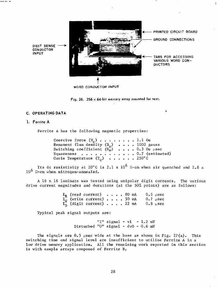
T e s t d a t a f o r l a m i n a t e d a r r a y s o f t h r e e s i z e s , 1 6 x 1 6 c r o s s o v e r s , 256 x 64 c ros sove r s , and 256 x 100 c rossove r s , are r e p o r t e d below. These laminates are o p e r a t e d w i t h b o t h word and d i g i t l i n e s g r o u n d e d a t one end, as shown i n Fig. 26. Sense ou tputs are monitored with a Tek t ron ix 1 1 2 1 a m p l i f i e r f e e d i n g a n o s c i l l o s c o p e . The o u t p u t d a t a f o r a g iven p l ane are t aken a t a f i x e d s t r o b e t i m e . The s t r o b e time is opt imized on the bas i s o f the peaking times f o r a few randomly s e l e c t e d b i t s .
Two di f fe ren t magnes ium-manganese-z inc fe r r i te composi t ions have been c o n s i d e r e d € o r u s e i n t h e low d r i v e memory. T h e i r c h a r a c t e r i s t i c s a n d s e n s e outputs ob ta ined f rom 16 x 16 p lanes are g iven next .
27
PRINTED CIRCUIT BOARD
GROUND CONNECTIONS
DIGIT SENSE CONDUCTOR INPUT
t WORD CONDUCTOR INPUT
TABS. FOR ACCESSING VARIOUS WORD CON- DUCTORS
Fig . 26. 256 x 64-bit memory array mounted for test.
C. OPERATING DATA .
1. Ferrite A
F e r r i t e A has t he fo l lowing magne t i c p rope r t i e s :
Coe rc ive fo rce (Hc) . . . . . . . . 1.1 Oe Remanent f l u x d e n s i t y (B,) . . . . 1000 gauss S w i t c h i n g c o e f f i c i e n t (S,) . . . . 0 . 3 O e psec Squareness . . . . . . . . . . . . 0.7 (es t imated) Curie Tempera'ture (T,) . . . . . . 250°C
I t s d c r e s i s t i v i t y a t 20°C i s 2.1 x l o 6 R-cm when a i r quenched and 2.8 x 10 6 R-cm when n i t rogen-annea led .
A 16 x 16 l amina te was t e s t e d u s i n g u n i p o l a r d i g i t c u r r e n t s . The v a r i o u s dr ive cur ren t magni tudes and dura t ions (a t t h e 50% p o i n t s ) are as fo l lows:
IR ( r e a d c u r r e n t ) . . . . 80 mA 0.5 psec Iw (write c u r r e n t ) . . . . 50 mA 0.7 psec ID ( d i g i t c u r r e n t ) . . . . 22 mA 0.8 psec
Typ ica l peak s igna l ou tpu t s a r e :
111" s i g n a l - v l - 1 . 2 mV Dis turbed "0" s i g n a l - dvO - 0.6 mV
The s igna l s a r e 0 .5 p sec w ide a t t h e b a s e a s shown in F ig . 27 (a ) . Th i s swi tch ing time and s i g n a l l e v e l are i n s u f f i c i e n t t o u t i l i z e Fer r i te A i n a low d r i v e memory a p p l i c a t i o n . A l l t he r ema in ing work r epor t ed i n t h i s s ec t ion i s wi th s ample a r r ays composed of F e r r i t e B.
28

Fig. 27. Experimental laminate operation.
2. Ferrite B
Ferrite B has the following magnetic properties:
H, = 0.4 Oe Br = 1200 gauss S, = 0.3 Oe psec
Tc = 110°C Squareness = 0.9
Its dc resistivity at 20°C is 8.6 x lo7 R-cm for air-quenched samples and 1.1 x LO8 R-cm for nitrogen-annealed samples.
A number of 16 x 16 laminates incorporating Ferrite B have been evaluated using a unipolar digit program [Fig. 25(a)]. The drive currents and their duration at the 50% points are:
IR (read current) . . . . 40 mA 0.5 psec Iw (write current) . . . . 35 mA 0.3 psec ID (digit current) . . . . 3 mA 0.5 psec
Typical peak signal outputs are:
"1" signal - vl = 1.4 mV Disturbed "0" signal - dvO = 0.4 mV
29

, . , _. , . , . .__.__ _ _ _ ... .. . .
The s i g n a l s are about 0 .3 psec wide a t t h e b a s e as shown in F ig . 27 (b ) .
A series of 256 x 64 and of 256 x 100 sample planes composed of F e r r i t e B have been fabr icated and evaluated using one or both of the pulse programs of F ig . 25 . Thei r charac te r i s t ics and per formance are g i v e n i n t h e n e x t s e c t i o n .
3. Kilo-Bit Array Performance
A l l o f t h e t e s t e d a r r a y s are composed of F e r r i t e B; t h e i r s i n t e r i n g termi- n a t e s w i t h e i t h e r a n a i r quench (air Q) o r a n i t r o g e n a n n e a l (N2 annea l ) . The s a m p l e p h y s i c a l c h a r a c t e r i s t i c s are g i v e n i n T a b l e I V .
The sample number "OS" i n T a b l e I V r e f e r s t o a l l f o u r 256 x 64 p lanes o f t h e "0" series u t i l i z e d t o f a b r i c a t e t h e p r o t o t y p e memory s t a c k s d e s c r i b e d i n S e c t i o n 111.
The o p e r a t i n g c h a r a c t e r i s t i c s o f t h e k i l o - b i t a r r a y s a r e p r e s e n t e d i n Table V. The t es t p u l s e s had t h e n o m i n a l d u r a t i o n s a t t h e 50% p o i n t s g i v e n below:
IR = r e a d c u r r e n t = 0.5 psec Iw = write c u r r e n t = 0 .4 p sec I = d i g i t c u r r e n t = 0.7 psec D
B i p o l a r d i g i t i n g i s denoted by the p resence o f bo th + and - s i g n s i n t h e ID column; f o r t h a t c a s e b o t h t h e 1 and 0 s i g n a l s are d i s t u r b e d a c c o r d i n g t o t h e program of Fig. 25(b). The r e a d c u r r e n t risetime i s 0.3 p s e c f o r 256 x 64 samples and 0.4 psec- for 256 x 100 samples.
It is c lear f rom the da ta o f Table V t h a t i n t h e o n e - c r o s s o v e r - p e r - b i t mode o f o p e r a t i o n , t h e a r r a y s r e q u i r e b i p o l a r d i g i t c u r r e n t s f o r r e l i a b l e sens ing .
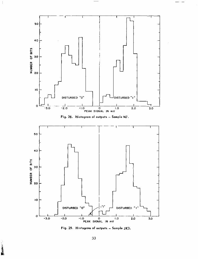
The u n i f o r m i t y o f b i t o u t p u t s f r o m p l a n e s w i t h a h igh pe rcen tage of b i - po l -a r ou tputs under condi t ions o f the b ipolar d ig i t p rogram is shown i n t h e h is tograms of F igs . 28, 29, and 30 for samples Mi', J K 3 , and JK12, r e s p e c t i v e l y . F o r t h e s e f i g u r e s , t h e o u t p u t s i g n a l s are q u a n t i z e d i n 0.2-mV s t e p s .
D. EFFECTS OF LAYER THICKNESS VARIATION ON ARRAY PERFORMANCE
Two o f t h e k i l o - b i t a r r a y s d e s c r i b e d i n t h e p r e v i o u s s e c t i o n h a v e s i g n i f - i c a n t l y d i f f e r e n t l a y e r t h i c k n e s s a r r a n g e m e n t s . All of the samples through t h e "M" series e x c e p t f o r M5 and M6, a re symmet r i ca l abou t t he cen te r l aye r , i.e., t h e f e r r i t e s h e e t s c o n t a i n i n g t h e word conduc to r s are e q u a l i n t h i c k n e s s t o t h o s e c o n t a i n i n g t h e d i g i t c o n d u c t o r s . Sample M5 h a s a n e x t r a 2 - m i l l a y e r o f f e r r i t e c o v e r i n g t h e word l ines whereas sample M6 has an addi t iona l 2 -mi l cove r ing ove r i t s d i g i t l i n e s . The super ior per formance of M5, obvious from Table V, i s a t t r i b u t e d t o t h e f a c t t h a t s w i t c h i n g d u e t o word c u r r e n t s now e x t e n d s a l l t h e way t o t h e s u r f a c e of the sample, as i l l u s t r a t e d i n F i g . 31.
30
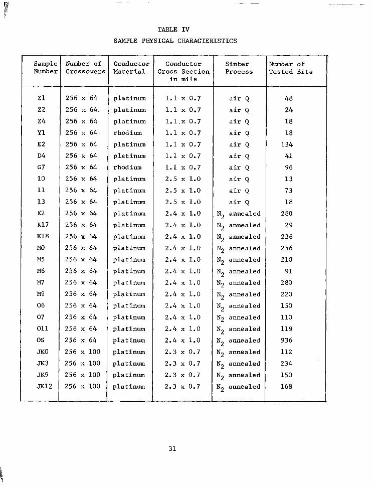
TABLE IV SAMPLE PHYSICAL CHARACTERISTICS
Sample Number
z1
22
24 Y1
E2
D4 G7 10
11
13 K2
K17 K18
MO
M5
M6
M7 M9
06
07 01 1
os JKO
JK3 JK9
x1 2
Number of Crossovers
256 x 64
256 x 64. 256 x 64 256 x 64 256 x 64 256 x 64 256 x 64 256 x 64 256 x 64 256 x 64 256 x 64 256 x 64 256 x 64 256 x 64 256 x 64 256 x 64 256 x 64 256 x 64
256 x 64 256 x 64
256 x 64 256 x 64 256 x 100
256 x 100
256 x 100
256 x 100
Conductor Material
platinum
platinum
platinum
rhodium
platinum
platinum
rhodium
platinum
platinum
platinum
platinum
platinum
platinum
platinum
platinum
platinum
platinum
platinum
platinum
platinum
platinum
platinum
platinum
platinum
platinum
platinum
Conductor Cross Section
in mils
1.1 x 0.7 1.1 x 0.7 1.1 . x 0.7 1.1 x 0.7
1.1 x 0.7 1.1 x 0.7 1.1 x 0.7
2.5 x 1.0
2.5 x 1.0
2.5 x 1.0
2.4 x 1.0
2.4 x 1.0 2.4 x 1.0
2.4 x 1.0
2.4 x 1.0
2.4 x 1.0
2.4 x 1.0
2.4 x 1.0
2.4 x 1.0
2.4 x 1.0
2.4 x 1.0
2.4 x 1.0 2.3 x 0.7 2.3 x 0.7 2.3 x 0.7
2.3 x 0.7
Sinter Process
air Q
air Q
air Q
air Q
air Q air Q air Q
air Q
air Q
air Q
N annealed
N2 annealed
N2 annealed N2 annealed N2 annealed N annealed
N2 annealed N2 annealed N annealed
N2 annealed N2 annealed N annealed
N2 annealed
N2 annealed N2 annealed N2 annealed
2
2
2
2
Number of Tested Bits
48
24 18 18 134 41 96
13
73 18
2 80
29
236 256 2 10
9 1
2 80
220
150 110
119
936 112
234 150
168
31
\
t

TABLE V SAMPLE OPERATING CHARACTERISTICS
SamPl€
z1 z 1 22
24
Y1 E2 E2
D4 D4 G7 10
11
11
13 K2
K17 K18 K18
MO M5
M6
M7
M9
06 07 011
JKO
JK3
JK9 JK12
-
IR - 36
36 36 36
36 40
40 40 40 40 63
50 50
52 50
42 45
47 52
48 48 50
50
50 50
50
50 48
50
50 -
IW - 16
16 12 19
20
16 20
20 20
17.5
37
17 20
26 18
26
30
34
23 20 18 20
20
20
24 26
18 20
20
20
ID - 2.3
- +2.3 1.8
1.9
5.5 1.8
+2.4 - 2.2
+2.2 - - +3.3 +6.5 - 11 12.5 +4 57.2
i5.5
7.5 4.0
i3.3
k6.0 - t5.5 i5.0 - t6.0 t5.0
k5.0 i5.1
t5.0
t5.0
t5.0 t5 .O
t5.0 -
Be vl
0.7 LO. 35
0.8
0.6
1.5 0.6
+0.4
0.7 +O. 4 +o. 2 -0.4
1.0
+o. 9 +O. 5
+2.2
0.8
1.8 +2.2
+2.2
+2.8 +l. 0
+2.0
+O. 8
+2.2 +2.0
+2.0
+1.4
+2.8
+1.2 +2.8
st
"
-
avo
0.2
-0.4 0.3
0.1
0.6 0.1
-0.4
0.2
-0.4 -0.3
+o. 2 0.4
+O. 3 -0.1
-2.0
0.3
0.8 -1.2 -2.6
-2.4 -1.2 -2.2
-1.0
-1.6
-3.2
-2.4 -1.8
-1.8
-1.2 -2.0
1
0.8
+0.2
0.9
0.8
1.5 0.7
bo. 5 0.8
+o. 2 -0.1
+0.3
1.3 +l. 0
+O. 3 +1.4 0.9
1.6 +0.8
+l. 5 "2 .o +1.0
+l. 5 +l. 0
+l. 0
+2.0
+1.7
+1.3 +1.6
+O. 8 +2.0
f+O .1
:a1 dvO
0.4 -0.4 0-5 0.3
1.0
0.3
-0.1 - O . 3 0.4 -0.5
-0.4 -0.1
0.6 +0.4 -0.1
t0.4 0.5
1.2 -0.6
-1.5 -2.0
-1.0
-1.5
t0.2
-1.0
-2.0
-1.7 -1.3
-1.6 -1.0
-2.0
T Percen t B i p o l a r ou tputs
"
37% "
"
"
"
5 1% -- 8 6%
30%
67% - L
-- 7 8% 44% -- "
80%
85%
97% 7 5% 99%
47%
99% 98% 92%
94%
98%
5 6% 100%
Peak Back Voltage
p e r b i t - mV
11.0
11.0
9.4 11.7
13.3
15.5
15.5 "
"
"
15
6.3
6.5 "
18.0 "
14.5 14.5 17.2
19.5 17.2 22.0 "
"
21.1 20.3 "
28.0 19.0
26.0
32
I
5 0 -
4 0 -
- t rn
$ 30
v)
-
a w m s 3 = 20-
-
5 0
4 0
v)
k m L 30
a m
z 20
0
w
5
I O
0
I
r
' r I L
DISTURBED " I "
-3.0 -2.0 - I .o 0 I .o 2 .o 3.0 PEAK SIGNAL IN mV
Fig . 28. Histogram of outputs - Sample M7.
1 DISTURBED "0"
I
r 9, DISTURBED * " I " {
-3.0 - 2.0 -1.0 0 I .o 2 .o 3.0 PEAK SIGNAL IN mV
L
Fig. 29. Histogram of outputs - Sample JK3.
33

v) k m
30 a m W
5 z 20
10
n
I I I I I
"
i
DISTURBED " I "
" L - 3.0 - 2.0 - 1.0 0 I .o 2.0 3.0 PEAK SIGNAL IN mV
5
Fig. 30. Histogram of outputs - Sample JK12.
\DIGIT CONDUCTOR
( a ) "SYMMETRIC" SAMPLE TO.002"
\DIGIT CONDUCTOR
( b ) SAMPLE M5
Fig. 31. Flux-switching regions (shaded) vs. layer thickness.
34
E. SOLID EPOXY STACK PERFORMANCE
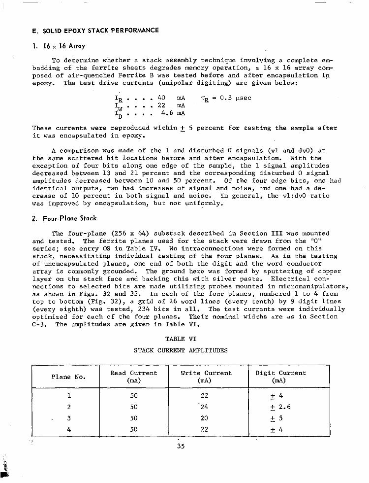
1. 16 X 16 Array
To determine whether a s tack assembly technique involv ing a complete em- b e d d i n g o f t h e f e r r i t e s h e e t s d e g r a d e s memory ope ra t ion , a 1 6 x 1 6 a r r a y com- posed of a i r -quenched Ferr i te B was t e s t e d b e f o r e a n d a f t e r e n c a p s u l a t i o n i n epoxy. The test d r i v e c u r r e n t s ( u n i p o l a r d i g i t i n g ) are given below:
1 R . m - 4 0 mA TR = 0 . 3 psec b.... 22 mA ID . . . . 4.6 mA
These cu r ren t s were reproduced wi th in +, 5 p e r c e n t f o r t e s t i n g t h e s a m p l e a f t e r it was encapsula ted in epoxy.
A comparison w a s made o f t he 1 and d i s turbed 0 s i g n a l s (vl and dvO) a t t h e same s c a t t e r e d b i t l o c a t i o n s b e f o r e and a f t e r e n c a p s u l a t i o n . W i t h t h e except ion of four b i t s a long one edge of the sample , the 1 s i g n a l a m p l i t u d e s decreased between 13 and 2 1 percen t and t he co r re spond ing d i s tu rbed 0 s i g n a l ampli tudes decreased between 10 and 50 percen t . Of t he fou r edge b i t s , one had i d e n t i c a l o u t p u t s , two had i n c r e a s e s of s i g n a l and noise, and one had a de- crease of 10 p e r c e n t i n b o t h s i g n a l and n o i s e . I n g e n e r a l , t h e v1:dvO r a t i o was improved by encapsula t ion , bu t no t un i formly .
2. Four-Plane Stack
The fou r -p l ane (256 x 6 4 ) s u b s t a c k d e s c r i b e d i n S e c t i o n I11 was mounted and tes ted . The f e r r i t e p l a n e s u s e d f o r t h e s t a c k were drawn from the "0" series; see e n t r y OS i n Table I V . No i n t r a c o n n e c t i o n s were formed on t h i s s t a c k , n e c e s s i t a t i n g i n d i v i d u a l t e s t i n g o f t h e f o u r p l a n e s . A s i n t h e t e s t i n g of unencapsulated planes, one end of b o t h t h e d i g i t a n d t h e word conductor a r r a y is commonly grounded. The ground here was formed by spu t t e r ing o f coppe r l a y e r on t h e s t a c k f a c e a n d b a c k i n g t h i s w i t h s i lver p a s t e . Electrical con- n e c t i o n s t o s e l e c t e d b i t s are made u t i l i z i n g p r o b e s mounted in micromanipula tors , as shown i n F i g s . 32 and 3 3 . I n e a c h o f t h e f o u r p l a n e s , numbered 1 t o 4 from top to bo t tom (F ig . 3 2 ) , a g r i d o f 26 word l i n e s ( e v e r y t e n t h ) by 9 d i g i t l i n e s ( eve ry e igh th ) w a s t e s t e d , 234 b i t s i n a l l . The tes t c u r r e n t s were i n d i v i d u a l l y opt imized for each of the four p lanes . Thei r nominal wid ths a re as i n S e c t i o n C-3. The ampl i tudes are g i v e n i n T a b l e V I .
TABLE V I
STACK C-NT AMPLITUDES
r" Plane No.
1
2
I I
Read Cur ren t Write Current
50
22 50
20 50
2 4 50
22
D i g i t C u r r e n t
+ 4 - +, 2.6
+ 5 - - + 4
35

Fig. 32. Four-plane stack mounted for test.
Fig. 33. Test apparatus for 4-plane stack.
36

I" "
The p e r c e n t a g e o f d i s t u r b e d b i p o l a r k i t o u t p u t s f o r t h e f o u r p l a n e s i s 57%, 63%, 64%, and 56% f o r P l a n e s 1, 2, 3, and 4 , r e s p e c t i v e l y . N o t e t h a t t h e t h r e e s i n g l y t e s t e d p l a n e s o f t h e "0" series had i n e x c e s s o f 90% b i p o l a r o u t - puts (Table V) . The phys ica l r eg ions where un ipo la r ou tpu t s are o b s e r v e d i n each of the four p lanes are denoted by shading in Fig. 34.
I .1
PLANE I PLANE 2
I
Fig. 34. Regions of unipolar outputs in prototype stack.
One e x p l a n a t i o n f o r t h e d a t a i s the presence of nonuniform stress i n t h e p lanes due to nonuni form adherence o f the epoxy to the l amina ted fe r r i te shee ts . This nonuniform adherence i s due, a t l e a s t i n p a r t , t o t h e h e a t i n g c y c l e s su f fe red by t h i s p ro to type s t ack du r ing t he coppe r spu t t e r ing expe r imen ta t ion . M i c r o s c o p i c i n s p e c t i o n o f t h e s t a c k f a c e s a f t e r s p u t t e r i n g r e v e a l e d r e g i o n s of nonadherence be tween epoxy and fe r r i te a t the s tack edges . A less l i k e l y a l t e r n a t i v e e x p l a n a t i o n i s t h a t t h e p l a n e s were inherent ly nonuniform.
F. EFFECT OF READ CURRENT WAVESHAPE ON SENSE SIGNALS
One of t h e b i t s i n s a m p l e K2 w i t h r e l a t i v e l y h i g h s e n s e o u t p u t w a s s e l e c t e d t o c h e c k t h e e f f e c t o f r e a d c u r r e n t a m p l i t u d e a n d risetime on t he s ense s igna l and back vol tage.8 To s e p a r a t e t h e e f f e c t s o f risetime and amplitude, two exper iments were performed: (1) The risetime was h e l d f i x e d a t 0 . 3 psec and the read cur ren t ampl i tude var ied f rom 20 t o 80 mA. (2) The r e a d c u r r e n t am- p l i t u d e was f i x e d a t 50 mA and the risetime var ied f rom 0.03 t o 0 . 4 p s e c . I n b o t h e x p e r i m e n t s t h e b i p o l a r d i g i t c u r r e n t s were h e l d f i x e d . The write c u r r e n t was o p t i m i z e d f o r maximum s e n s e s i g n a l i n t h e f i r s t e x p e r i m e n t i n w h i c h t h e r e a d c u r r e n t a m p l i t u d e was v a r i e d .
37

Figure 35 shows the dependence of sense s igna l ampl i tude ( so l id curve) and switching time, TS (de f ined as time f rom beg inn ing o f r ead pu l se t o . end o f s e n s e o u t p u t ) , on r e a d c u r r e n t a m p l i t u d e . The anomalous d i p i n T a t 30 mA i s due t o a d e c r e a s e i n optimum wri te c u r r e n t w h i c h i n t u r n r e s u l t s I n h i g h e r peak sense s igna l bu t lower sense f lux . Note the g radual l eve l ing o f f of sense s i g n a l a m p l i t u d e as t h e s w i t c h i n g ' t i m e -rS approaches the risetime of t he r ead pulse . The back vo l tage due to f lux-swi tch ing c l imbs f rom 9.4 mV/bit a t 50-mA r e a d c u r r e n t t o 18 mV/bit a t 80-mA read cu r ren t whereas t he s ense s igna l goes from 4.7 mV to 6 mV, a marked d r o p i n " e f f i c i e n c y " .
8
Fig. 35. Effect of read amplitude on signal.
Figure 36 shows tha t t he s igna l magn i tude i s r e l a t i v e l y i n s e n s i t i v e t o t h e risetime, o n l y d o u b l i n g f o r a 4 : l change i n T ~ . C o n c u r r e n t l y , t h e b i t b a c k v o l t a g e i n c r e a s e s f i v e f o l d .
G. DISTURB SENSITIVITY
One o f t h e b i t s i n Sample 07 was u t i l i z e d t o c h e c k t h e d i s t u r b c h a r a c t e r - i s t ics o f t h e s a m p l e s f o r d i s t u r b b u r s t s o f l e n g t h g r e a t e r t h a n t h e t h r e e w h i c h a r e u s e d i n t h e s t a n d a r d b i p o l a r d i g i t p r o g r a m o f F i g . 2 5 ( b ) . The pulse p ro- gram i s shown i n F i g . 37. The t es t c u r r e n t d a t a are given below:
Current Ampli tude Durat ion Risetime
IR IW ID
50 0.8 0.2
20 0.6 0.2
v a r i e s 1 .5 -"
38

I -
Fig. 36. Effect of read risetirne on signal.
WORD CONDUCTOR -="ma-
READ WRITE WRITE
READ DISTURBED SIGNAL . SIGNAL
UNDISTURBED
""_ U READ
T I M E - DIGIT A . I ""
CONDUCTOR I ""_ .
DlQlT D IGIT D IGIT D ISTURB BURST OF LENGTH N
Fig. 37. Disturb burst program.
Oscillograms of the disturbed and undisturbed signal waveforms are shown in Fig. 38 for a long disturb burst, N = 170,000 pulses. The polarities and amplitudes of the digit pulses used for writing ("digit") and the digit pulses used for disturbing ("digit disturb") are given in Fig. 38. A single digit disturb, N = 1, degrades the undisturbed signal by one half as much as the long
39
. ....

d v l Uvl d v l
( a ) D i g i t = -5 mA (b ) D ig i t = -5 mA Digit DLsturb = +5 m.4 D i g i t D i s t u r b = -6 mA
d : O I
uvo
(c) D i g i t = +5 mA D i g i t D i s t u r b = -5 mA
d ;O I
uvo
( d ) D i g i t = +5 mA D i g i t D i s t u r b = -6 mA
Horiz . Sca le : 1 .0 psec /d iv . Vert. Sca le : 5 mV/div.
Fig. 38. Disturb behavior of Sample 07.
b u r s t . N o t e t h a t i n F i g s . 3 8 ( b ) a n d ( d ) t h e d i s t u r b i n g d i g i t i s 20 pe rcen t g rea t e r i n magn i tude t han t he nomina l d ig i t u sed fo r wr i t i ng (5 mA). However, a d i sce rnab le s igna l r ema ins . A 50 p e r c e n t g r e a t e r d i s t u r b ( i . e . , 7 . 5 mA) i s s u f f i c i e n t t o " k i l l " t h e s i g n a l .
H. NOISE CHARACTERISTICS
Ohmic, capac i t ive , and induct ive coupl ing be tween the word d r ive and t he d i g i t - s e n s e c o n d u c t o r s r e s u l t i n e x t r a n e o u s n o i s e d u r i n g r e a d t i m e .
1. Ohmic Coupling
The coupl ing res i s tance be tween a word conductor and a sense -d ig i t con - ductor ranges f rom 2 .5 x l o 7 R t o 250 x lo8 R (computed f o r a n assumed f e r r i t e r e s i s t i v i t y r a n g i n g f r o m 1 0 5 t o lo8 R-cm). T h e s e c o u p l i n g r e s i s t o r s l e a d t o
40
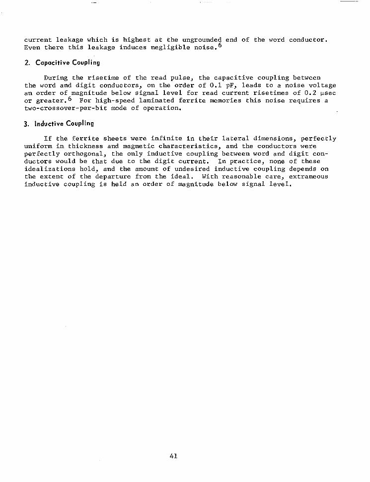
cur ren t l eakage wh ich i s h ighes t a t the ungrounded end of the word conductor. Even t h e r e t h i s l e a k a g e i n d u c e s n e g l i g i b l e n o i s e . 6
2. Capacitive Coupling
During the risetime of the read pu lse , the capac i t ive coupl ing be tween t h e word and d ig i t conduc to r s , on t he o rde r o f 0 .1 pF, l e a d s t o a n o i s e v o l t a g e an order of magni tude below s ignal level f o r r e a d c u r r e n t risetimes of 0 .2 psec o r g r e a t e r . 6 F o r h i g h - s p e e d l a m i n a t e d f e r r i t e m e m o r i e s t h i s n o i s e r e q u i r e s a two-crossover -per -b i t mode of opera t ion .
3. Inductive Coupling
I f t h e f e r r i t e S h e e t s were i n f i n i t e i n t h e i r l a t e r a l d i m e n s i o n s , p e r f e c t l y u n i f o r m i n t h i c k n e s s and magnet ic charac te r i s t ics , and the conductors were pe r fec t ly o r thogona l , t he on ly i nduc t ive coup l ing be tween word and d i g i t con- duc to r s wou ld be t ha t due t o t he d ig i t cu r ren t . I n p rac t i ce , none o f t hese i d e a l i z a t i o n s h o l d , a n d t h e amount of undesired induct ive coupl ing depends on the ex ten t o f the depar ture f rom the idea l . Wi th reasonable care , ex t raneous i n d u c t i v e c o u p l i n g i s he ld an o rder o f magni tude be low s igna l l eve l .
41

V. RADIATION STU Dl ES
A. FACILITIES
A f i v e - m e g a w a t t , p o o l - t y p e n u c l e a r r e a c t o r a t t h e I n d u s t r i a l R e a c t o r L a b o r a t o r i e s , I n c . (IRL), i n P l a i n s b o r o , New Jersey (approximate ly two miles I
n o r t h e a s t o f RCA L a b o r a t o r i e s ) h a s b e e n u s e d t o s t u d y t h e e f f e c t o f n e u t r o n r a d i a t i o n o n b o t h f e r r i t e m a t e r i a l s a n d f i e l d - e f f e c t t r a n s i s t o r s . I R L i s j o i n t l y owned by RCA and n ine o the r co rpora t ions , and t h e r e a c t o r i s o p e r a t e d by Colombia Universi ty . Normally, the reactor i s i n o p e r a t i o n f o r a 90-hour period each week.
The pr imary purpose of the I R L r e a c t o r i s t o p r o v i d e a source o f neut rons , gamma r a y s a n d r a d i o a c t i v e i s o t o p e s f o r e x p e r i m e n t a t i o n . It provides a number of loca t ions where spec imens may b e p l a c e d o r e x p e r i m e n t s c o n d u c t e d t o u t i l i z e t h e r a d i a t i o n s . T h e s e i n c l u d e :
1. One 12-inch square and one 8-inch diameter beam tube, and four 6- inch diameter beam t u b e s , e x t e n d i n g f r o m t h e o u t s i d e v e r t i c a l w a l l s o f t h e p o o l t o t he f ace o f t he co re , wh ich may be u sed i n water- o r a i r - f i l l e d c o n d i t i o n s w i t h a p p r o p r i a t e s h i e l d p l u g s . Two beam t u b e s a r e c u r r e n t l y i n u s e by RCA. They have a working diameter of 1-1/8 inch and a re 14-1 /2 fee t long . For t e s t s d u r i n g r a d i a t i o n s , f i b e r - g l a s s - i n s u l a t e d a l u m i n u m l e a d s a t l e a s t 1 4 - 1 / 2 f e e t l o n g a r e r e q u i r e d .
2 . A h o r i z o n t a l t h e r m a l column, f o u r f e e t s q u a r e i n c r o s s s e c t i o n , f i l l e d wi th s t r i n g e r s o f h i g h - p u r i t y g r a p h i t e , w h i c h makes a v a i l a b l e a wide range of f l uxes o f "slow" o r " the rma l i zed" neu t rons .
3 . Two pneumat ic " rabbi t" tubes which pass a longs ide the core for con- venien t shor t exposures o f smal l samples .
4 . Space in the water a round the reac tor and unused pos i t ions in the core g r i d p l a t e w h i c h may be used for spec imen i r rad ia t ion .
5. Gamma i r r a d i a t i o n f a c i l i t i e s o u t s i d e t h e p o o l a r e a u s i n g t h e r e a c t o r f u e l e l e m e n t s a s t h e s o u r c e o f r a d i a t i o n .
6 . Gama i r r ad ia t ion i n t he poo l f rom fue l e l emen t s wh ich have been i n t h e r e a c t o r c o r e .
RCA h a s i t s own l a b o r a t o r y f a c i l i t i e s a t IRL, and a s t a f f o f i t s own p e r - s o n n e l c a r r i e s o u t i t s ind iv idua l r e sea rch p rog ram.
I n a d d i t i o n t o v a r i o u s h e a v i l y s h i e l d e d f a c i l i t i e s f o r t h e s t o r a g e and hand l ing o f r ad ioac t ive ma te r i a l s t ha t have been exposed i n t he r eac to r , t he ' ' ho t " l abo ra to ry accommoda t ions i nc lude t h ree spec ia l c e l l s i n which experiments can be handled by "master-s lave" mechanical manipulators . Each of these c e l l s i s cons t ruc t ed o f h igh -dens i ty conc re t e , 3 f e e t t h i c k , f a c e d w i t h s t e e l s k i n s , wi th access th rough doors weighing 13 tons each .
42

C h a r a c t e r i s t k s o f t h e two loca t ions where the exper iments were c a r r i e d o u t are given i n Table VII, where " f a s t " n e u t r o n s a r e d e f i n e d h e r e as t h o s e having an energy greater than 500 eV.
TABLE VI1
IRRADIATION CONDITIONS
"- "~ . .. - ~ . ~ ~ ~~ ~~ ~ ~
Neutrons cm s e c -2 -1
Max. Exposure F a s t
1.5 x 10 lOI3 A t Core ( i n wa te r )
13 l . x 10 Hydraul ic Rabbi t
p e r Run Therma 1 = " - "" . . . ~ . ~~
1 hour
90 hours 13 ~ ~. . . . . . . - . " ~ -. "
B. FERRITE COMPONENTS
1. Introduction
Exper iments were conducted to de te rmine the e f fec t o f neut ron rad ia t ion on t h e f u n d a m e n t a l p h y s i c a l p r o p e r t i e s o f f e r r i t e s A and B ( d e s c r i b e d i n S e c t . I V ) . The b a s i c p r o p e r t i e s s t u d i e d b e f o r e a n d a f t e r i r r a d i a t i o n a r e : c o e r c i v e f o r c e Hc, r emanent f lux dens i ty B r , h y s t e r e s i s l o o p s q u a r e n e s s , e l e c t r i c r e s i s t i v i t y p, and d i e l e c t r i c E .
2. State of the Art
Ceramics ( f e r r i t e s b e l o n g t o t h e c e r a m i c f a m i l y ) a r e q u i t e r a d i a t i o n - r e ~ i s t a n t . ~ The damage mechanism i n f e r r i t e s i s thought to be d i sp lacement o f t h e m e t a l i o n s , t h u s c a u s i n g v a c a n c i e s a n d i n t e r s t i t i a l s i n t h e s p i n e l s t r u c - t u r e .
Some work has been done on squa re - loop f e r r i t e s su i t ab le fo r memory appl icat ions.10-12 Sery e t a l . 1 ° s tud ied 50 -50 N i f e r r i t e and found small changes (10 percent a t most) i n t h e c o e r c i v e f o r c e H, and the f l u x d e n s i t y Br. Mos's e t al .11 i n v e s t i g a t e d f a s t - s w i t c h i n g m a g n e s i u m - m a n g a n e s e f e r r i t e s a f t e r exposures up to 3 x 1 O I 8 n v t ( f a s t n e u t r o n s ) . They found changes i n t h e h y s t e r e t i c p r o p e r t i e s (H, increased and Br d e c r e a s e d ) a f t e r 1018 nvt bu t no change i n the switching speed. Taimuty and Mills12 measured t he r ad ia t ion s e n s i t i v i t y o f two magnesium-manganese memory cores (Ferramic S1 and S 3 ) a s w e l l a s a v a r i e t y o f m i c r o w a v e f e r r i t e s . The memory c o r e s e x h i b i t e d s l i g h t ( a l m o s t w i t h i n e x p e r i m e n t a l e r r o r ) i n c r e a s e s i n Hc and even smal le r increases i n B r . I n a p r e v i o u s s t u d y o n f e r r i t e r e s i s t i v i t y c h a n g e s a f t e r i r r a d i a t i o n , a va r i e ty o f n i cke l - z inc and manganese -z inc commerc ia l f e r r i t e s were exposed t o a s i m u l a t e d n u c l e a r b u r s t .13 Although the mpyentary neutron dose had high i n t e n s i t y t h e i n t e g r a t e d f l u x was low, up t o 10 nv t i nc lud ing t he rma l s , and n o m e a s u r a b l e e f f e c t o n r e s i s t i v i t y was found.
43
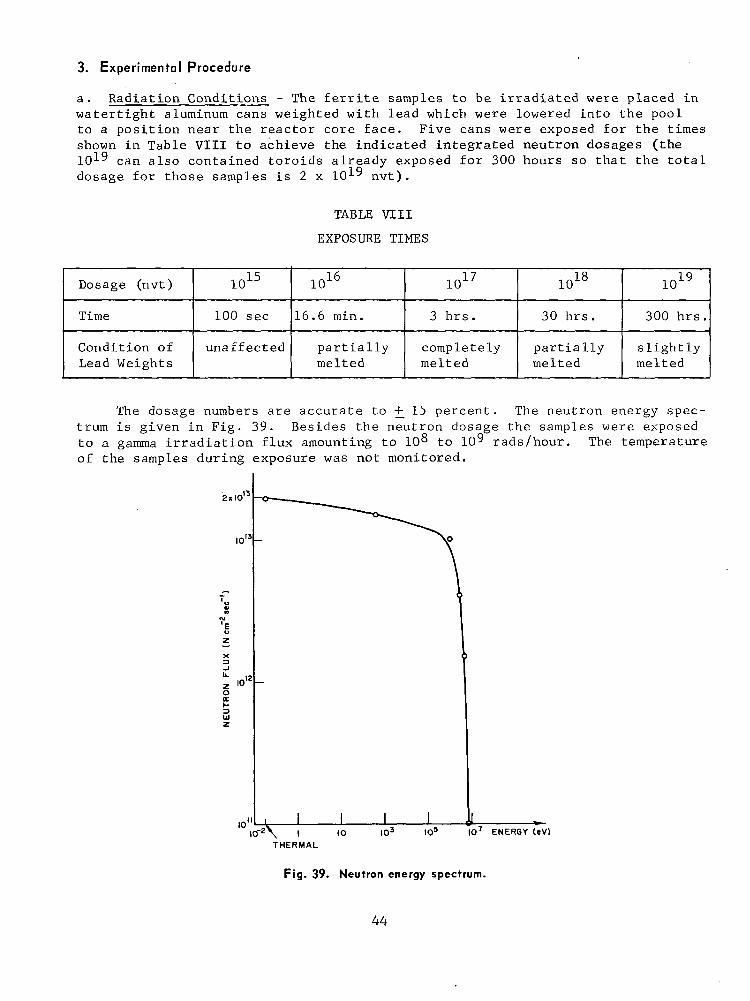
3. Experimental Procedure
a . R a d i a t i o n C o n d i t i o n s - The f e r r i t e s a m p l e s t o b e i r r a d i a t e d were p l a c e d i n w a t e r t i g h t aluminum cans weighted with lead which were lowered in to the pool t o a p o s i t i o n n e a r t h e r e a c t o r c o r e f a c e . F i v e c a n s were exposed for the times shown i n T a b l e V I 1 1 t o a c h i e v e t h e i n d i c a t e d i n t e g r a t e d n e u t r o n d o s a g e s ( t h e
c a n a l s o c o n t a i n e d t o r o i d s a l r e a d y e x p o s e d f o r 300 hours s o t h a t t h e t o t a l dosage fo r t hose s amples i s 2 x 10¹⁹ nv t ) .
TABLE VI11
EXPOSURE TIMES
Dosage (nvt) 1 oI8 1019 1 -
Time
m e l t e d mel ted mel ted mel ted Lead Weights s l i g h t l y p a r t i a l l y c o m p l e t e l y p a r t i a l l y una f fec t ed Cond i t ion of
300 h r s . 30 h r s . 3 h r s . 16.6 min. 100 sec
The dosage numbers a r e a c c u r a t e t o f 15 pe rcen t . The neut ron energy spec- trum i s g iven in F ig . 39 . Bes ides the neut ron dosage the samples were exposed t o a gamma i r r a d i a t i o n f l u x a m o u n t i n g t o lo8 t o l o 9 r a d s / h o u r . The temperature of the samples dur ing exposure was not monitored.
THERMAL
Fig. 39. Neutron energy spectrum.
44
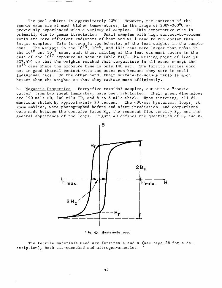
The pool ambient i s approximately 4OoC. However, t h e c o n t e n t s o f t h e s a m p l e c a n s a r e a t much h ighe r t empera tu res , i n t he r ange o f 200°-300°C a s p rev ious ly expe r i enced w i th a var ie ty o f samples . This t empera ture r i s e i s p r i m a r i l y d u e t o gamma i r rad ia t ion . Smal l samples wi th h igh sur face- to-volume r a t i o a r e more e f f i c i e n t r a d i a t o r s o f h e a t and w i l l t e n d t o r u n c o o l e r t h a n l a rge r s amples . This i s seen i n t he behav io r o f t he l ead we igh t s i n t he s ample cans . The w e i g h t s i n t h e 1015, and 1017 cans were l a r g e r t h a n t h o s e i n t h e 1OI8 and lo1' cans , and , thus , mel t ing of t he l ead was mos t s eve re i n t he c a s e o f t h e 1 0 1 7 e x p o s u r e a s s e e n i n T a b l e VIII. The mel t ing po in t o f l ead i s 327.4OC so t h a t t h e w e i g h t s r e a c h e d t h a t t e m p e r a t u r e i n a l l c a s e s e x c e p t t h e 1015 case where the exposure t ime i s only 100 sec . The f e r r i t e samples were n o t i n good the rma l con tac t w i th t he ou te r can because t hey were i n s m a l l i n d i v i d u a l c a n s . On the o the r hand , t he i r su r f ace - to -vo lume r a t io i s much b e t t e r t h a n t h e w e i g h t s s o t h a t t h e y r a d i a t e more e f f i c i e n t l y .
b . Magne t i c P rope r t i e s - For ty - f ive t o ro ida l s amples , cu t w i th a "cookie cu t te r" f rom two shee t l amina tes , have been fabr ica ted . Thei r g reen d imens ions a r e 1 9 0 mils OD, 140 m i l s I D , and 6 t o 8 m i l s t h i c k . Upon s i n t e r i n g , a l l d i - mensions shr ink by approximately 20 p e r c e n t . The 400-cps hys t e re s i s l oops , a t room ambient, were pho tographed be fo re and a f t e r i r r ad ia t ion , and comparisons were made be tween t he coe rc ive fo rce Hc, t he r emanen t f l ux dens i ty B r , and t h e genera l appearance o f t h e l o o p s . F i g u r e 40 d e f i n e s t h e q u a n t i t i e s o f Hc and B r .
Fig. 40. Hysteresis loop.
The f e r r i t e m a t e r i a l s u s e d a r e f e r r i t e s A and B (see page 2 8 f o r a d e - sc r ip t ion) , bo th a i r -quenched and n i t rogen-annea led . *
45

c . E l e c t r i c P r o p e r t i e s - To d e t e r m i n e r e s i s t i v i t y and d i e l e c t r i c c o n s t a n t changes, samples i n t h e f o r m of c a p a c i t o r s were f a b r i c a t e d . S i n t e r e d s h e e t s o f f e r r i t e 3 i n . x 1 i n . x 2-3 m i l s t h i c k were coated with an a luminum evap- o r a t e d . l a y e r 2000-3000 8 i n t h i ckness . Samples app rox ima te ly 0.2 i n . x 0 . 2 i n . were c u t f r o m t h e s h e e t s , g i v i n g a p r e - i r r a d i a t i o n c a p a c i t a n c e o f r o u g h l y 50 pF.
The dc conduc t iv i ty was determined by measuring the current drawn by the sample from a 6-V dry c e l l w i t h a Boonton microammet,er. The capac i tance was measured by a General Radio type 716-C impedance br idge. To g e t s u f f i c i e n t Q t o o p e r a t e t h e b r i d g e a c c u r a t e l y , t h e m e a s u r i n g f r e q u e n c y was s e t a t 100 kc / sec ( t h e h i g h e s t c o n d u c t i v i t y f e r r i t e r e q u i r e d 3 0 0 k c / s e c ) . To in su re cons t an t and r ep roduc ib le t empera tu re and a h i g h Q the measurements a re made wi th t he s ample c o o l e d i n a double thermal ba th as shown. in F ig . 41.
Two s e p a r a t e r u n s w e r e made w i t h t h e c a p a c i t o r s a m p l e s . I n Run I t h e l e a d s were a t t ached t o t he s ample (u s ing a t i n - z i n c s o l d e r ) , i n i t i a l m e a s u r e - ments made, leads removed, samples i r rad ia ted , l eads re -a t tached , and samples re-measured. Also , t h e i n n e r t h e r m a l b a t h c o n t a i n e d s i l i c o n e o i l r a t h e r t h a n n-hexane as shown i n F i g . 4 1 . I n Run I1 t h e a luminum l eads were l e f t a t t ached throughout and the inner thermal ba th was changed to t he n -hexane .
f l TO BRlDGElMlCROAMMETER
BEAKER HOLDER \
KER ML
k - H E X A N E )
AND ICE MIXTURE SATURATED BRINE
Fig. 41. Double thermal bath.
4. Experimental Results and Discussion
a . Magne t i c P rope r t i e s - P e r c e n t a g e c h a n g e s i n t h e h y s t e r e t i c p r o p e r t i e s Br and Hc ( s e e F i g . 4 0 ) a r e p r e s e n t e d i n F i g s . 42 t o 49 f o r t h e f o u r f e r r i t e s , namely f e r r i t e A a i r -quenched and n i t rogen-annea led , r e spec t ive ly , and f e r r i t e B a i r -quenched and ni t rogen-annealed, respect ively. The percentage changes a re computed a c c o r d i n g t o t h e r e l a t i o n s h i p :
46
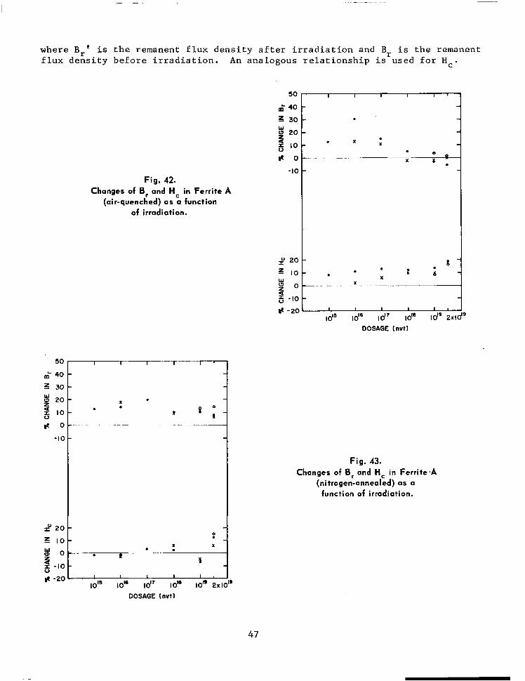
where B r ' i s t h e r e m a n e n t f l u x d e n s i t y a f t e r i r r a d i a t i o n and Br i s the remanent f l u x d e n s i t y b e f o r e i r r a d i a t i o n . An ana logous r e l a t ionsh ip i s used for Hc.
50
&- 40
3 30
z 0
Y 20 2 10
-10
2 20 z 10
E
Fig. 42. Changes of Br and Hc in Ferrite A
(air-quenched) a s a function of irradiation.
.
0
m' 40 - 30 -
3 20 - g l 0 -
e 0 -
-10 -
I" 20 3 l 0 -
-
w P O - 6 -10 -
.
X ".
e -201 I I I I I ,
lob5 lot7 lolo 1olg 2 x 1 DOSAGE (nvt )
Fig. 43. Changes of Br and H, in Ferrite ,A
(nitrogen-annealed) as a function of irradiation.
9
DOSAGE (nvt)
47

5 0
& 4 0
z 30 20
W
z 2 I O
6 0 -10
60
50
v 40
g 30 I:
$! 2 0
10
0
-10
- 2 0
2
0
6
I I I I I '
X
X x . . ' x . * "" ~
X
X
8 *L
X
I I 1 I I L
1015 toI6 10'' 1 0 ' ~ lot9 2 DOSAGE (nvt 1
Fig. 45. Changes of Br and Hc in Ferrite B
(nitrogen-annealed) as a function of irradiation.
F ig . 44. Changes of Br and Hc in Ferrite B
(air-quenched) as a function of irradiation.
9
50
& 40
z 30 9 20 a
$ 0
-10
5 10
I" 2 0
E o 9 -10
g I O
z 0 6 -20
I I I I I '
X
X " " .
f
DOSAGE (nvt )
48
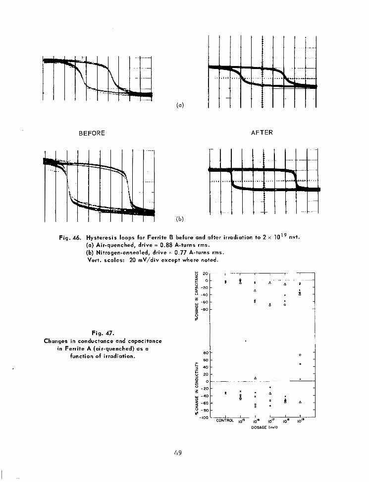
BEFORE AFTER
Fig. 46. Hysteresis loops for Ferrite 6 before and after irradiation to 2 x 10¹⁹ nvt. (a) Air-quenched, drive = 0.88 A-turns rms. (b) Nitrogen-annealed, drive = 0.77 A-turns rms. Vert. scales: 20 mV/div except where noted.
Fig. 47. Changes in conductance and capacitance
in Ferrite A (air-quenched) as a function of irradiation.
DOSAGE (nvt l
49

Fig. 48. Changes in conductance and capacitance
in Ferrite A (nitrogen-annealed) as a function of irradiation.
DOSAGE ( n v t )
20 z I I I I I I
u ' - 4 0 -
2 0
P z
5 0 0 - 2 -20 - . ". *" "* - "4." .... ~
0 o A
-60 - ! * (3
I 3 -80 -
x 0
:: -
160
- 140
- 0 - -
120 - X
Fig. 49. 100 - X - Changes in conductance and capacitance 80 -
in Ferrite B'(air-quenched) 2 5 60
as a function of irradiation. 3
- - B 4 0 - 8 2 0 -
w o
-
z -
P -20- ! i 7---:- 0
a 3 - 4 0 -
B o 0
3 -
-60
- - 8 0
- - -
-100 1 I I I I I CONTROL lol' IoIC lola
DOSAGE (nvt)
50

The numbers co r re spond ing t o t he da t a po in t s i n F igs . 42 t o 50 a r e g i v e n i n T a b l e s I X and X. The d a t a p o i n t s i n t h e f i g u r e s a r e i n d i c a t e d b y b l a c k
w 20 V
* o i! Y -20 3 -40
1 -60
(3 -80 w z 0 9 +!
>- k E 20
2 0 8 - 2 0
V
z
z -40
(3 -60 w z 0 9 -80 st -100
1 . 1 I I I I
0 n n a 0
X 0 0
0 . X X 0
a It
0 X 0
! I I I I I
CONTROL lo16 ,017 1019
DOSAGE (nvt)
Fig. 50. Changes in conductance and capacitance in Ferrite B (nitrogen-annealed) as a function of irradiation.
d o t s , c i r c l e s , a n d c r o s s e s t o d i f f e r e n t i a t e b e t w e e n t h e d i f f e r e n t t o r o i d a l s a m p l e s s u b j e c t e d t o t h e same neut ron exposure . For ins tance , on the g raphs of F i g . 42 t h e two c r o s s e s a t 1018 nv t co r re spond t o t he change i n B r and Hc i n one s ample and t he do t s a t 1OI8 n v t c o r r e s ond t o t h e c h a n g e s i n a n o t h e r sample. A given symbol a t t h e d o s a g e 2 x l 0 l G nv t i s f o r t h e same Sam l e a s the corresponqhng symbol a t n v t , ( e . g . , t h e f o u r b l a c k d o t s a t 10E9 n v t and a t 2 x 10 n v t a r e f o r t h e same sample exposed i n two separa te runs o f
each ) . This correspondence does not hold a t any of t he o the r dosages .
The p o s s i b l e s o u r c e s o f e r r o r i n t h i s e x p e r i m e n t a r e : 1. N u m e r i c a l i n t e r p r e t a t i o n of o sc i l l og rams 2 . Changes i n room ambient temperature 3 . Gain d r i f t i n e l e c t r o n i c c i r c u i t r y 4 . E r r o r i n r e p r o d u c i n g d r i v i n g c u r r e n t s
51

TABLE I X
RADIATION EFFECTS ON FERRITE A - MAGNETIC PROPERTIES
Air-Quenched
Ni t rogen - Annea l e d
Sample #
10
8
9
6
7
4
5
1
2
3
1
2
3
30
28
29
2 7
24
25
2 1
22
23
2 1
22
23
Dosage nvt
1oI6
10l6
lo18
2 x 10
2 x 10
2 x 10
19
1 9
1 9
10l6
10l6
10l8
2 x 10
2 x 10
2 x 10
19
19
1 9
%Change Br
12.8
30.6
12.5
15.3
10.8
5 . 0
-2.4
3 .6
-3.3
-2.3
1.2
-5.5
0
12.3
17.8
14.3
2 0
15
14.6
11.7
12.5
10
5 .9
14.3
8 .3
%Change Hc
8.5
11.0
2.1
12.8
6.2
12.2
9.8
12.8
13.7
9.6
17 .0
17.9
18.0
-1.3
-2.5
-1.3
3.6
2.4
6 . 3
-5.7
-5.9
-6.3
5.7
15.3
12.5
52

TABLE X
RADIATION EFFECTS ON FERRITE B - MAGNETIC PROPERTIES
Air-Quenched
Ni t rogen - Annea l e d
Sample #
45
43 44
4 1
42
14
15
17
12
13
12
13
39
38
37
35
36
32
33
33
Dosage nvt
10 l6
1oI6
10l8
10l8
10l8
l o L 9 2 x 10
2 x 10
19
1 9
1oI6
10l8
2 x 10 19
%Change Br
19
27.5
13.6
29.4
38.9
14.8
14.8
9.5
28.3
22.2
20.8
25.9
20.5
13.9
20
8.4
7.5
2.5
3.6
-3.6
%Change H C
-11.9
1.5
1.5
1 .3
-4.4
7.4
5.4
9.3
17.8
60.4
46.5
56.6
-6
-4.9
-4.1
-6.5
-4.9
-5.5
1.8
7.3
53

Ind iv idua l ly , none o f t hese e r ro r s wou ld be expec ted t o exceed +, 5 p e r - c e n t . A c c o r d i n g t o t h e l i t e r a t u r e o n e w o u l d e x p e c t i n s i g n i f i c a n t c h a n g e s a t l eas t over the range of 1015 - 1017 nv t . Thus , t hese po in t s s e rve a s a rough c a l i b r a t i o n .
F igu res 4 2 and 4 3 i n d i c a t e i n s i g n i f i c a n t c h a n g e s i n t h e f l u x d e n s i t y Br o f f e r r i t e A a f t e r e x p o s u r e s a s h i g h a s 2 x 10’’ nvt.;: I t s c o e r c i v e f o r c e Hc increases by roughly 10 p e r c e n t a t 2 x 10‘’ n v t . F e r r i t e B a l s o shows s i g - n i f i c a n t c h a n g e s i n B r o v e r t h e f u l l d o s a g e r a n g e , a s s e e n i n F i g s . 44 and 45. T h e c o e r c i v e f o r c e o f t h e a i r - q u e n c h e d f o r m o f f e r r i t e B i n c r e a s e s by about 5 0 p e r c e n t a t 2 x lo1’ n v t w h i l e t h e Hc of the ni t rogen-annealed form remains e s s e n t i a l l y c o n s t a n t . T h i s d i f f e r e n c e may be due to neutron-induced s t ress r e l i e f i n t h e quenched f e r r i t e .
The shapes o f t he ‘ l oops be fo re and a f t e r i r r ad ia t ion were r emarkab ly s i m i l a r , a s i l l u s t r a t e d by Fig. 46.
To summar ize , i n t eg ra t ed neu t ron dosages a s h igh a s 2 x 10 nvt can be t o l e r a t e d by t h e s e f e r r i t e w i t h o u t s i g n i f i c a n t l y a l t e r i n g t h e m a g n e t i c p r o p - e r t ies , w i t h the s o l e e x c e p t i o n o f t h e a i r - q u e n c h e d f o r m o f f e r r i t e B .
19
b . E l e c t r i c P r o p e r t i e s - P e r c e n t c h a n g e s i n t h e c a p a c i t o r t e r m i n a l p r o p e r t i e s - - c a p a c i t a n c e C, and d c c o n d u c t i v i t y G a r e g i v e n i n F i g s . 47 t o 5 0 f o r t h e f o u r f e r r i t e t y p e s . The pe rcen t changes a r e computed ana logous ly t o Equa t ion (1). Numbers c o r r e s p o n d i n g t o t h e d a t a p o i n t s i n F i g s . 47 t o 50 a r e g i v e n i n Tables X I , X I I , X I I I , and XIV. The d a t a i n c l u d e c o n t r o l s a m p l e s a l l o f w h i c h were produced a t t h e same t i m e a s t h e i r r a . d i a t e d s a m p l e s . Some of these con- t r o l s w e r e h e a t e d a t . 225’C f o r 9 0 h o u r s .
Most o f t h e d a t a i n t h e f i g u r e s c o r r e s p o n d t o Run 11 where t he l eads were l e f t a t t a c h e d . The da t a po in t s co r re spond ing t o Run I a r e i n d i c a t e d by t r i - a n g l e s . The remain ing symbols a re used s imply to d i f fe ren t ia te be tween the var ious samples o f the same f e r r i t e t y p e s u b j e c t e d t o t h e same neut ron exposure .
The p o s s i b l e s o u r c e s o f e r r o r i n t h i s e x p e r i m e n t a r e : 1. microammeter reading 2. br idge r ead ing 3. n u l l l o c a t i o n f o r c a p a c i t a n c e b r i d g e 4 . t e m p e r a t u r e r e p r o d u c i b i l i t y 5. sneak conduction paths via sample holder 6 . de t e r io ra t ion o f a luminum con tac t s .
The f i r s t t h r e e s h o u l d n o t l e a d t o a t o t a l e r r o r o f more than 5 t o 10%. The nominal bath temperature i s -8.5OC. The measured var ia t ion i s -9OC t o -7.5OC. The t e m p e r a t u r e v a r i a t i o n o f f e r r i t e c o n d u c t a n c e i s approximately 2 0 pe rcen t ove r t he 1.5OC r ange . The f i f t h item, sneak conduct ion, i s p a r t i c - u l a r l y n o t i c e a b l e i n r e m e a s u r i n g i r r a d i a t e d s a m p l e s . The person moving samples
:’: The anomalous point a t 1016 nv t i n F ig . 42 i s p r o b a b l y d u e t o a n e r r o r i n t h e number of secondary tu rns used to ob ta in the B-H loop. For that sample t h e o r i g i n a l Br v a l u e i s cons ide rab ly l ower t han fo r s imi l a r s amples .
5 4

Sample #
7
18
20
‘ 22
13
14
15
19
1 2
28
34
10
16
1 7
5
6
‘9
11
40
30
39
TABLE XI
RADIATION EFFECTS ON FERRITE A (AIR-QUENCHED) ELECTRICAL PROPERTIES
Dosage nvt
10 l6
1oI6
10 l6
10l8
10l8
10l8
1 oI9 c o n t r o l
h e a t e d c o n t r o l
h e a t e d c o n t r o l
$Change c
- 3.9
0
0
+ 2.6
-55.8
-58.7
- 4 . 1
- 6.9
- 4
-65
-68.7
-68.5
-57.5
-4 1
-11.1
-28
-35.4
- 7.8
- 5.9
- 2.8
- 4.5
$Change PA
-41.2
-38 .O
-28.5
-51.0
-71.2
-64.5
-42.8
-32.4
-17.5
-69 .O
-53.8
-53
-51.1
-42.4
+ 4.9
“46.7
“72.5
“45.8
-31
-34.2 ---
55

Sample #
18
19
2 3
24
9
22
32
36
10
25
27
13
26
28
16
1 7
2 9
30
2 0
40
34
39
TABLE X I 1
RADIATION EFFECTS ON FERRITE A
(NITROGEN-ANNEALED) ELECTRICAL PROPERTIES
Dosage n v t
1ol6
1 oI6 1 oI6
10l8
10l8
1ol8
c o n t r o l
c o n t r o l
hea t e d con t ro 1
h e a t e d c o n t r o l
%Change C
-12.8
- 3.8
- 4.9
- 7.7
-80.4
-62
-71.5
-68
-48.4
-72.9
-72.6
-84
-77
-79
-59.5
-74
-70.2
-71.4
-36.2
0
-46.1
-47.6
%Change PA
-34.2
-5 0
-41.3
-40.5
-93
-76.8
-70
-68.8
-42.5
-77.8
-58.4
-95.5 ---
-68
-30.4
"- -43.5
-69.6
-58.7
-29.4
-60
+ 6.7
56

" ." -
Sample #. "
9
14
1 7
25
10
36
37
39
2
6
23
30
7
12
16
24
3
19
26
29
27
32
40
TABLE XI11 RADIATION EFFECTS ON FERNTE B
(AIR-QUENCHED) ELECTRICAL PROPERTIES
~
Dosage . . nvt
10l6
10l6
10l6
10l6
10l8
10l8
10l8
1oI8
contro 1
control
h e a t e d control
~
%Change c ""
0
+ 1
+ 2.6
0
- 4.7
-18.2
-29.2
0
0
-53.4
-31.2
-14.3
-72.1
-56.7
-61.8
-53.2
-50.7
-60.5
70.7
-52.4
-18.1
0
-11.8
%Change MA
- '14.3
- 23.4
- 10.7
- 22
- 3.9
- 2.5
- 2.2
- 10.9
- 15
- 52.7
+ 7
- 33.4
+ 117
+ 55
+ 162 "
- 11.1
- 18 --
+ 94.5
- 11.1
- 14.7
+ 31.3
57

RA h D I AT1 ON
Sample #
15
22
24
35
3
4
9
13
6
8
11
20
16
37
39
27
29
30
34
17
2 3
7
18
TABLE X I V
EFFECTS ON FERRITE B (NITR
ELECTRICAL PROPERTIES
"
.OGEN-ANNEALED)
Dosage nvt
10l6
1 0 l 6
10 l6
1 oI8 10l8
10l8
c o n t r o l
c o n t r o l
h e a t e d c o n t r o l
h e a t e d c o n t r o l
%Change C
- 2 .1
0
0
+ 2 .1
0
-53.4
-48
- 8.2
+ 4 .1
-5 3
+ 1.8
-63.5
-72.6
-54.5
-47.6
-65.7
-69.6
-36.4
-42.6
-26.2
+ 2.71
-35.6
- 6.30
%Change WA
-20.9 "-
-41.4
-30.6
-25
-61.8 "-
-42.5
-22.8
-5 7
-34.7 "-
-39.6
-27.8 "-
-35.2
-19.5 -" -"
-20 "-
-55
-30.4
58

i n and ou t o f t he s ample ho lde r wea r s d i sposab lepo lye thy lene g loves a s a pre- cau t ion aga ins t rad ioac t ive contaminat ion . These g loves readi ly p ick up contaminants which can be b rushed of f on to the sample ho lder l ead ing to sneak c u r r e n t s a s h i g h a s s e v e r a l m i c r o a m p e r e s . When t h i s e f f e c t was noted dur ing the second run the conductances were remeasured , per iodica l ly checking the sneak c u r r e n t t o i n s u r e t h a t i t was w e l l below 0.1 PA. However, i t i s p o s s i b l e t h a t t h e s e s n e a k c u r r e n t s were p r e s e n t t n some e x t e n t i n t h e p r e - i r r a d i a t i o n m e a s u r e - ments. They were n o t l a r g e t h e n , however, because some samples had o r i g i n a l c u r r e n t s o f 0.4 t o 0 . 5 P A . I n add i t ion , t he s amples chosen fo r i r r ad ia t ion had a h igh deg ree o f cons i s t ency i n bo th t he i r capac i t ance and conduc tance .
The l a s t e r r o r s o u r c e , c o n t a c t d e t e r i o r a t i o n , i s by f a r t h e most s i g n i f i - c a n t . T h i s d e t e r i o r a t i o n i s n o t a t t r i b u t a b l e s o l e l y t o n e u t r o n and gamma f l u x because samples that were not exposed had the same s o r t o f symptoms, a l though n o t a s o f t e n a n d n o t t o s u c h e x t r e m e s . The scope of the e f fec ts on unexposed samples i s shown i n F i g . 5 1 . The sample i n F i g . 5 1 ( c ) h a s b e e n h e a t e d t o 225OC i n a i r f o r 90 hours . The o t h e r t h r e e were aged a t room ambient . As a p recau t ion ,
( 4 ( 4 Fig. 51. Aging effects on aluminum contact appearance.
59

i t should be no ted tha t the photos overemphas ize the g rada t ions in darkness because of t h e h i g h c o n t r a s t p r i n t s . The d a r k r e g i o n s i n F i g . 51 (d) appear v i s u a l l y o n l y a s d a r k a s t h e d a r k r e g i o n s i n F i g . 5 1 ( b ) . The sample shown i n F i g . 5 1 ( a ) i s normal in appearance, i . e . , l i k e a f r e s h l y made sample. Since the s amples have h igh r e s i s t ance (200 kR and up) , the contac t can be qu i te poor be fo re t he conduc tance and capac i t ance measu remen t s a r e a f f ec t ed . However, i n a c a s e l i k e F i g . 5 1 ( d ) the d a r k r i n g a r o u n d t h e s o l d e r a r e a c a n b e a t o t a l i n t e r r u p t i o n i n a luminum con t inu i ty , t hus r educ ing t he con tac t a r ea qu i t e s ig - n i f i c a n t l y . T h i s r e s u l t s i n a l a rge pe rcen tage d rop i n bo th capac i t ance and conductance. Many of the exper imenta l samples showed such a d r o p i n b o t h c a p a c i t a n c e a n d c o n d u c t a n c e , a s i l l u s t r a t e d i n F i g s . 47 t o 50. S ince t he phys - i c a l mechanisms f o r c o n d u c t a n c e a n d c a p a c i t a n c e i n s o l i d s a r e q u i t e d i f f e r e n t , i t i s improbable tha t a g i v e n n e u t r o n d o s e w o u l d a f f e c t b o t h p r o p e r t i e s b y t h e same p e r c e n t a n d i n t h e same d i r e c t i o n . It i s t h e r e f o r e l i k e l y t h a t s a m p l e s which suf fe red rou h ly equal d rops in capac i tance and conduct iv i ty ( for example , t h e " c r o s s " a t lo1' n v t i n F i g . 50) d id s o b e c a u s e o f c o n t a c t d e t e r i o r a t i o n .
To summarize, large downward changes (> 10 p e r c e n t ) i n c a p a c i t a n c e c a n b e caused by c o n t a c t d e t e r i o r a t i o n a n d / o r t h e e f f e c t o f n e u t r o n s a n d gamma r a y s o n t h e m a t e r i a l d i e l e c t r i c c o n s t a n t . Downward changes i n conduc t iv i ty can be due t o some combination o f contac t de te r iora t ion , t empera ture change , and the e f f e c t o f r a d i a t i o n o n f e r r i t e c o n d u c t i v i t y . Upward changes i n c o n d u c t i v i t y c a n b e d u e t o t e m p e r a t u r e c h a n g e a n d / o r t h e e f f e c t o f r a d i a t i o n o n f e r r i t e c o n d u c t i v i t y .
Figures 47 and 48 i n d i c a t e i n s i g n i f i c a n t c h a n g e s i n t h e d i e l e c t r i c c o n s t a n t c f f e r r i t e A . The c o n d u c t a n c e o f f e r r i t e A i n c r e a s e s by abou t 50 pe rcen t fo r the air-quenched form and by about 20 p e r c e n t f o r t h e n i t r o g e n - a n n e a l e d f o r m a t 1019 n v t .
F igu res 49 and 50 ind ica te downward c h a n g e s i n d i e l e c t r i c c o n s t a n t by 2 0 t o 40 p e r c e n t f o r f e r r i t e B a t 1018 nv t wi th no fur ther change a t LO1' n v t . The c o n d u c t a n c e o f f e r r i t e B in a i r -quenched form roughly doubles a t 1 O l 8 nv t w h i l e t h e n i t r o g e n - a n n e a l e d v e r s i o n c h a n g e s l i t t l e .
The g e n e r a l t r e n d f o r m o d e r a t e i n c r e a s e s i n c o n d u c t a n c e may b e t h e r e s u l t of a s e c o n d a r y e f f e c t . We do know t h a t t h e c o n d u c t i o n i n a l l t h e s e f e r r i t e s i s n - type , i . e . , i t i s p r i m a r i l y d u e t o e l e c t r o n i c t r a n s p o r t . F o r h i g h - r e s i s t i v i t y f e r r i t e s , s u c h a s f e r r i t e s A and B, t h e i r o n i o n s p r e s e n t must be f e r r i c - I f t h e n e u t r o n and gamma f l u x c a u s e o x i d a t i o n of t h e aluminum film, some o f t h i s oxygen may be drawn f rom the ferr ic ions, thus changing them t o f e r r o u s a n d the reby i nc reas ing t he conduc t iv i ty v i a t he mechan i sm o f e l ec t ron hopp ing be - tween f e r r i c a n d f e r r o u s i o n s .
To s u m m a r i z e , t h e c h a n g e s i n e l e c t r i c p r o p e r t i e s o f t h e s e f e r r i t e s a f t e r e x p o s u r e t o n v t a r e n o t l a r g e e n o u g h t o a f f e c t memory ope ra t ion , because t h e memory performance i s n o t v e r y s e n s i t i v e t o m o d e r a t e c h a n g e s i n t h e s e p r o p e r t i e s .
60

C. RADIATION STUDIES ON MOS TRANSISTORS
1. State of the Art
R e l a t i v e l y few r a d i a t i o n s t u d i e s h a v e b e e n c o n d u c t e d o n s i l i c o n f i e l d - e f f e c t t r a n s i s t o r s . Most s t u d i e s a r e o n t h e r e v e r s e - b i a s e d p - n j u n c t i o n g a t e v a r i e t y . Comparisons between t h i s t y p e a n d p l a n a r b i p o l a r s i l i c o n ( c o n v e n t i o n a l ) t r a n - s i s t o r s do n o t g i v e a t r u e p i c t u r e b e c a u s e o f t h e i r d i f f e r e n t c o n s t r u c t i o n s .
Most o f t he pe r fo rmance deg rada t ion ( cu r ren t ga in r educ t ion ) i n b ipo la r t r a n s i s t o r s i s d u e t o a r e d u c t i o n o f t h e m i n o r i t y - c a r r . i e r l i f e t i m e a n d c a n therefore be min imized th rough the use o f a t h i n b a s e r e g i o n a s u s e d i n h i g h - f r e q u e n c y d i f f u s e d - b a s e t r a n s i s t o r s . F i e l d - e f f e c t t r a n s i s t o r s a r e m a j o r i t y - c a r r i e r d e v i c e s and do no t su f f e r f rom minor i ty -ca r r i e r l i f e t ime p rob lems . R a d i a t i o n a t h i g h l e v e l s (> l oL5 nv t ) r educes t he ma jo r i ty -ca r r i e r mob i l i t y and t h e r e f o r e t h e t r a n s c o n d u c t a n c e o f t h e f i e l d - e f f e c t t r a n s i s t o r . M e t a l - o x i d e semiconductors (MOS) i n s u l a t e d - g a t e f i e l d - e f f e c t t r a n s i s t o r s a l s o s u f f e r f r o m p o s s i b l e c h a r g e b u i l d - u p i n t h e o x i d e l a y e r t h u s s h i f t i n g t h e t r a n s f e r c h a r a c - t e r i s t i c ( d r a i n c u r r e n t v e r s u s g a t e v o l t a g e ) . S e c o n d a r y e f f e c t s may cause an i n c r e a s e i n t h e l e a k a g e of t h e g a t e j u n c t i o n s o r t h e i n s u l a t e d g a t e and t h e s o u r c e a n d d r a i n j u n c t i o n s .
D i f f e r e n t t y p e s o f r a d i a t i o n s r e s u l t i n d i f f e r e n t amounts of damage t o t h e semiconductor devicef4 Table XV shows t h e r e l a t i v e e f f e c t i v e n e s s o f t h e v a r i o u s t y p e s o f r a d i a t i o n s . The accuracy i s no b e t t e r t h a n a f a c t o r o f 2 t o 3 . For r e a s o n s o f e a s y a v a i l a b i l i t y , m o s t r a d i a t i o n s t u d i e s i n t h e l i t e r a t u r e u s e neut ron or e lec t ron bombardment .
S . M. C h r i s t i a n o f RCA L a b o r a t o r i e s i r r a d i a t e d s e v e r a l "765 r e v e r s e - b i a s e d g a t e f i e l d - e f f e c t t r a n s i s t o r s , w h i c h c a n a l s o b e o p e r a t e d a s pnp b i p o l a r t r a n s i s t o r s . ; ' : W h i l e t h e f i e l d - e f f e c t mode i s n o t a f f e c t e d by a d o s e a s h i g h a s l o L 4 n v t , t h e b i p o l a r o p e r a t i o n shows d e g r a d a t i o n a t l e v e l s a s low a s 10" nv t i (Th i s does no t mean t h a t r a d i a t i o n - r e s i s t a n t b i p o l a r t r a n s i s t o r s c a n n o t b e d e s i g n e d t o s t a n d n v t r a d i a t i o n l e v e l s . )
I n i t i a l n e u t r o n r a d i a t i o n s t u d i e s up t o 1015 nvt conducted by S . M . C h r i s t i a n on MOS f u l l - g a t e l o w - l e v e l l o g i c t r a n s i s t o r s showed d a t a w i d e l y s c a t t e r e d . Some performance degradat ion was n o t e d a t d o s e s s l i g h t l y h i g h e r t h a n t h o s e t o l e r a t e d by h i g h - f r e q u e n c y b i p o l a r t r a n s i s t o r s .
C . Gross and C . Fa les have observed a d ra in cu r ren t dec rease o f va r ious 15
degrees on RCA expe r imen ta l n and p enhancement type MOS t r a n s i s t o r s . T h e s e t r a n s i s t o r s were exposed t o 22-MeV p ro tons , 0 .3 and 2-MeV e l ec t rons . N- type c h a n n e l u n i t s d i d no t deg rade w i th 0.3 M e V e l e c t r o n s a t a dose of 3 x 1OI6 el/cm . However they degraded to 70 pe rcen t I d r a i n w i t h 2-MeV e l e c t r o n s a t a dose of 4 x 10¹⁵ el/cm2. Bombardment w i t h 22-MeV p r o t o n s r e d u c e d t h e d r a i n c u r r e n t t o 7 0 percent o f i t s o r i g i n a l v a l u e a t a dose of 2 .5 x lo1' p/cm2.
2
;t S . M. C h r i s t i a n ; t o b e p u b l i s h e d a c h a p t e r i n F i e l d - E f f e c t T r a n s i s t o r P h y s i c s , Devices , Fundamenta l and Appl ica t ions , Pren t ice Hal l , Inc .
61

TABLE XV RELATIVE EFFECTIVENESS OF NUCLEAR PARTICLES AT VARIOUS ENERGIES FOR
PRODUCING DISPLACEMENT DAMAGE IN SILICON AND GERMANIUM
Particle
Therma 1 Neutron
Fission Neutron
Neutron
Neutron
Gamma Photon
Electron
Electron
Electron
Proton
Proton
Proton
Deuteron
A 1 pha
Energy (MeV)
2.5 x
1 to 2 4.8
14
1.25
0.3
1.0
4.5
17.6
110
740
9.6
40 ~~.
Relative Effectiveness for Silicon
1.0
4 x
2.5 x
5 x
0 ,. 02
1.2
0.4
0.6
1.0
10
Relative Effectiveness for Germanium
3.1 x
1.0
1.2
0.8
4 x
0.02
2 00
H. L. Hughes and R. R. Girouxl' recently published degradation results of commercial n- and p-type MOS transistors for Cobalt" gamma irradiation. lo6 rads absorbed radiation reduced transconductance to less than one third of its original value. In none of the articles mentioned above was the effect of afterexposure annealing studied.
2. Device Geometry and Device Properties
For operating a laminated ferrite memory, driver MOS transistor strips with center-to-center spacings of 10 mils are required. A top view of such a unit is shown in Fig. 52. Several segments of the MOS driver strip were mounted in 10-lead TO5 headers with 4 drain, 4 gate, 1 common source, and 1 substrate con- tacts. As little gold as possible was used to avoid the radiation of the slowly decaying Au198 (half-life 2.70 d). Each can contains four n-type enhancement MOS transistors with a channel width of 120 mils, a channel length between 0.17 and 0.25 mil and a substrate resistivity of 10-Rcm p-type.
In initial batches indium solder between the nickel-plated posts of the stem and the gold wire was used for thermocompression bonding. A typical drain current/drain voltage characteristic is shown in Fig. 53(a). The silicon dioxide is doped for device stabilization and device characteristics are usually reproducible at temperatures up to 100°C.
62
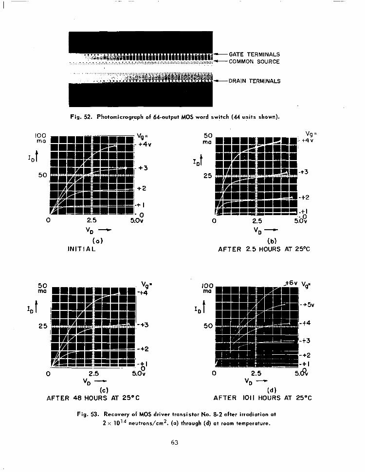
100 ma
1 t 50
Fig. 52. Photomicrograph of 64-output MOS word switch (44 units shown).
Vg = ' + 4 v
' +3
50 ma
25
+2
.+ I
. n 0 2.5 5.0;
VD - ( 0 )
INITIAL
50 ma
2 5
0 2.5 5.0'; VD -
(c) AFTER 48 HOURS AT 25OC
vg = - + 4 v
-t3
-t2
-t I 0 2.5 5.0 v
'I 0
"D - (b)
AFTER 2.5 HOURS AT 25OC
-+5v
- t4
-+2 .+ I
0 2.5 5.& vo -
( d l AFTER 1011 HOURS AT 25OC
Fig. 53. Recovery of MOS driver transistor No. 8-2 after irradiation at
2 x 10¹⁴ neutrons/cm2. (a) through (d) a t room temperature.
63

100 ma
ID t 50
+ 5 v Vg =
+4v
+3
+2
+ I 0 2.5 5.0 v
'D - AFTER 23 HOURS AT 100°C
( e )
IO 0 ma
I D t 50
v = 9
+ 4 v
+3
+2
+I 2.5 5 . 0 ~ 0
"D - AFTER 91 HOURS AT I00"C
( f 1
'D - 'D - ( g ) ( h )
AFTER 253 HOURS AT 10o"C AFTER 470 HOURS AT I00"C
Fig. 53. Recovery of MOS driver transistor No. 8-2 after irradiation at
2 x 10¹⁴ neutrons/crn2. (e) through (h) a t 100%
64

t 6 v +5 100 ma
50
Y
+ 4 v
+3
+2
+I 0
0 2.5 5 . 0 ~
VD - ( i )
AFTER I '/2 HOURS AT 14OoC
0 2.5 5.0 v
VD - Cj 1
AFTER 6 'I2 HOURS AT 14OoC
IO 0 ma
I D t 5 0
+6 +5v Vq =
+4v
+3
+2
+ I 0
0 2.5 5 .Ov
vo - ( k )
A F T E R 22 HOURS AT 140°C
Fig. 53. Recovery of MOS driver transistor No. 8-2 after irradiation at
2 x 10¹⁴ neutrons/cm2 (i) through (k) a t 140%.
65

3. Neutron-Radiation-Induced Effects
r a d i a t i o n up t o t h e 3 x 10¹⁵ neutrons/cm2. Figure 54 shows t h e e f f e c t o f t h e d i f f e r e n t d o s e s o n t h e t r a n s f e r c h a r a c t e r i s t i c . The measurements were t aken 5 t o 1 6 d a y s a f t e r i r r a d i a t i o n . The d r a i n c u r r e n t d e c r e a s e s r a t h e r d r a s t i c a l l y w i t h r a d i a t i o n level.
The same MOS t r a n s i s t o r s were s u b j e c t e d t o i n c r e a s i n g d o s e s o f n e u t r o n
DRAIN CURRENT @ V'd = +4v
4 100 ma
-
50 -
+I + 2 +3 + 4 v GATE VOLTAGE
Fig. 54. Change of transfer characteristic of MOS driver as a function of radiation dose.
It soon became a p p a r e n t t h a t t h e i n t r i n s i c d e g r a d a t i o n i s d i f f i c u l t t o m e a s u r e s i n c e a n n e a l i n g t a k e s p l a c e i f t e r (and even during) exposure. A def in i te dependence on t h e l o c a t i o n o f t h e s a m p l e s d u r i n g i r r a d i a t i o n was ob- se rved . MOS t r a n s i s t o r s i n t h e p n e u m a t i c r a b b i t t u b e g e t l e s s h e a t i n g a n d fewer x-rays and show more d e g r a d a t i o n t h a n u n i t s p l a c e d i n t h e swimming pool c l o s e t o t h e r e a c t o r c o r e f a c e . For t h e 3 x 10¹⁵ dose the samples were placed i n t h e p o o l . The remaining data were obtained using the pneumatic tube.
From then on t he dev ice cha rac t e r i s t i c s were measu red a s soon a s i t was p o s s i b l e t o h a n d l e t h e r a d i o a c t i v e u n i t s a f t e r e x p o s u r e ; ? and to mon i to r t he d a t a a s a func t ion o f t ime a t t empera tu res o f 25OC, 100°C, and 140OC. Figure 53 shows t h e V - I c h a r a c t e r i s t i c s a t v a r i o u s s t a g e s o f r e c o v e r y , and F igs . 55 and 56 show t h e d r a i n c u r r e n t o f a t y p i c a l u n i t a s a funct ion of t ime and temperature . R e l a t i v e l y f a s t r e c o v e r y e x i s t s up t o 10 h o u r s a t room tempera ture , a f te r which i t i s ve ry s low. Ra i s ing t he t empera tu re t o 100°C l eads t f u r t h e r r e c o v e r y . A p l o t o f t h e t r a n s f e r c h a r a c t e r i s t i c s ( i n t h i s c a s e en v s . Vgate) i s more meaningful and i s p l o t t e d i n F i g . 57. An o f f s e t v o l t a g e ok about -0.9 v o l t i s obta ined by l i n e a r l y e x t r a p o l a t i n g f r o m l a r g e g a t e v o l t a g e s . E x p o s u r e t o 2 x 1 0 1 4 n e u t r o n s / c m 2 s h i f t s t h e t r a n s f e r c h a r a c t e r i s t i c o f t h i s p a r t i c u l a r
6 6

I oc mA
0
sc a
w
J 4
2 x 10'4NEUTRONS/cmZ VSD = - 4 v
- I v, =+4v
I 1 I I A I I I 2
A IO 100 1000 ' IO IO0 'I IO I
HOURS AT ROOM TEMF! HOURS A T 100°C HOURS AT 14OoC
Fig. 55. Drain current of MOS transistor No. 8-2 as a function of time and temperature after 2 x 10¹⁴ neutrons/cm2 irradiation.
0
Fig. 56. Drain current at zero gate bias of MOS transistor No. 8-2 as a function of time and temperature after 2 x 10l4 neutrons/cm2 irradiation.
67

G IO -
Jmc;;
5 - @ 2 r / , hrs. AT 25O (AFTER IRRAD.)
"0 I 2 3 4 5 "GATE VOLTS
Fig . 57. Transfer characteristic of MOS transistor No. 8-2 as a function of temperature after 2 x 10¹⁴ neutrons/cm2 irradiation.
u n i t by approximate ly + 1.6 v o l t s ( c u r v e 2 i n F i g . 5 7 ) . F u r t h e r a n n e a l i n g a t room t e m p e r a t u r e s h i f t s t h e t r a n s f e r c h a r a c t e r i s t i c b a c k by abou t -0 .5 vo l t (curves 3 and 4 i n F ig . 57 ) . Annea l ing a t 100°C inc reases t he s lope o f t he t r a n s f e r c h a r a c t e r i s t i c , i n d i c a t i n g a n i n c r e a s e i n c h a n n e l m o b i l i t y ( c u r v e s 5-7 i n F i g . 5 7 ) . The MOS t r a n s i s t o r i m p r o v e d f u r t h e r ( c u r v e s 8 - 1 0 i n F i g . 5 7 ) . The un i t s t e s t ed wen t t h rough a maximum a t 14OoC but p ro longed hea t ing e v e n t u a l l y r e d u c e d t h e d r a i n c u r r e n t . S i n c e t h i s i s t r u e f o r i r r a d i a t e d t r a n - s i s t o r s a n d n o n i r r a d i a t e d c o n t r o l samples , the t rans is tor cans were opened and s e v e r e m e t a l l u r g i c a l d e g r a d a t i o n was observed.
In F ig . 58 , ind ium migra t ion a long the go ld wires and onto some of the chromium-silver s t r i p c o n t a c t s c a n be seen. Capaci tance measurements a lso c o n f i r m t h a t o n l y p a r t of the MOS t r a n s i s t o r s (1, 3 and 4 shown i n F i g . 5 8 )
68
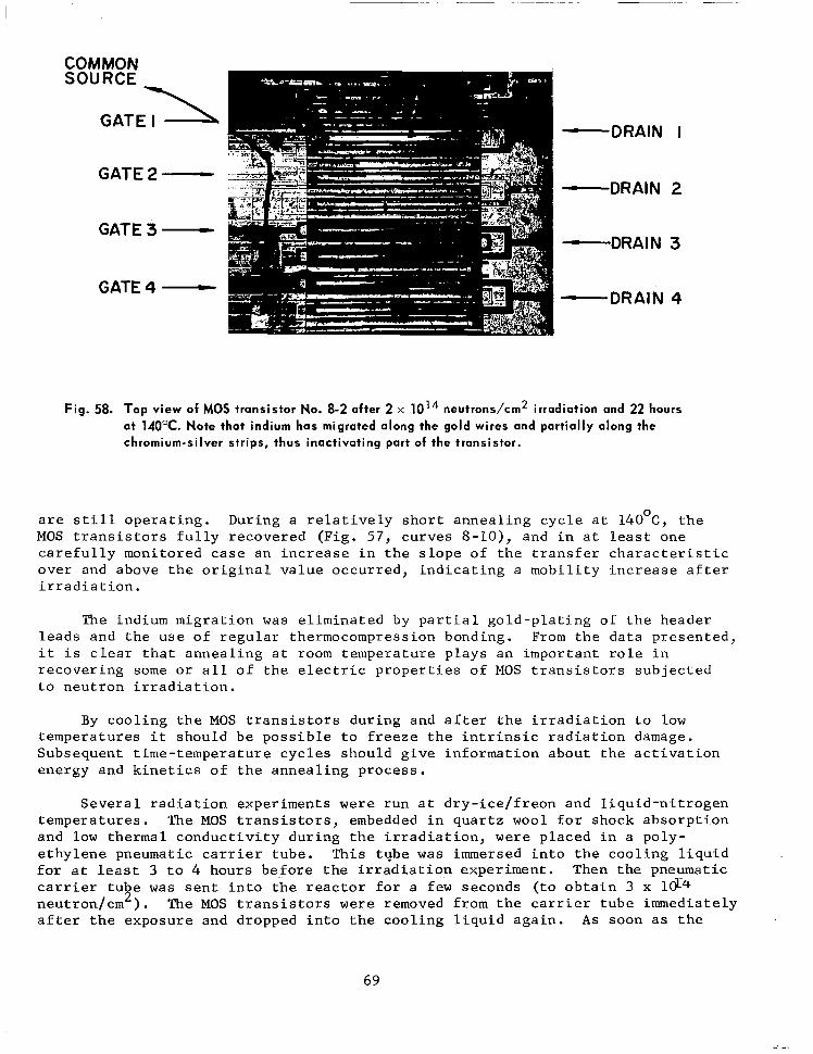
GATE 2 - GATE 3 - GATE 4 -
- DRAIN I
-DRAIN 2
-DRAIN 3
-DRAIN 4
Fig. 58. Top view of MOS transistor No. 8-2 after 2 x 10¹⁴ neutrons/cm2 irradiation and 22 hours at 140°C. Note that indium has migrated along the gold wires and partially along the chromium-silver strips, thus inactivating part of the transistor.
are still operating. During a relatively short annealing cycle at 140 C, the MOS transistors fully recovered (Fig. 57, curves 8-10), and in at least one carefully monitored case an increase in the slope of the transfer characteristic over and above the original value occurred, indicating a mobility increase after irradiation.
0
The indium migration was eliminated by partial gold-plating of the header leads and the use of regular thermocompression bonding. From the data presented, it is clear that annealing at room temperature plays an important role in recovering some or all of the electric properties of MOS transistors subjected to neutron irradiation.
By cooling the MOS transistors during and after the irradiation to low temperatures it should be possible to freeze the intrinsic radiation damage. Subsequent time-temperature cycles should give information about the activation energy and kinetics of the annealing process.
Several radiation experiments were run at dry-ice/freon and liquid-nitrogen temperatures. The MOS transistors, embedded in quartz wool for shock absorption and low thermal conductivity during the irradiation, were placed in a poly- ethylene pneumatic carrier tube. This tube was immersed into the cooling liquid for at least 3 to 4 hours before the irradiation experiment. Then the pneumatic carrier tu e was sent into the reactor for a few seconds (to obtain 3 x l&4 neutron/cm ). The MOS transistors were removed from the carrier tube immediately after the exposure and dropped into the cooling liquid again. A s soon as the
'3
69
J 2.
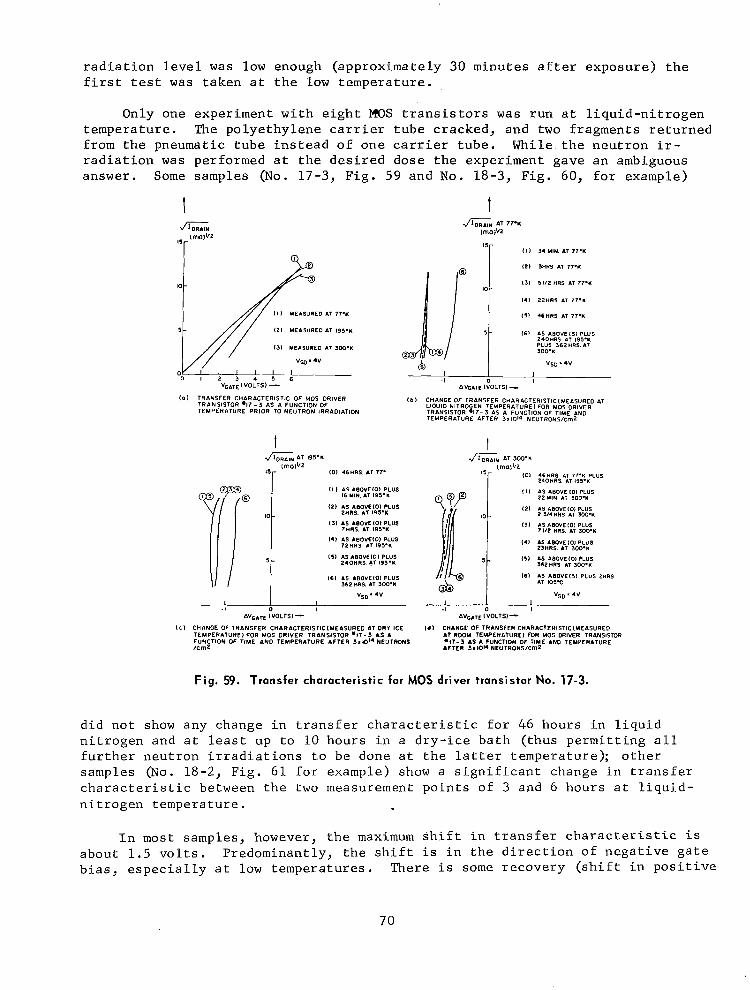
radiation level was low enough (approximately 30 minutes after exposure) the first test was taken at the low temperature.
Only one experiment with eight MOS transistors was run at liquid-nitrogen temperature. The polyethylene carrier tube cracked, and two fragments returned from the pneumatic tube instead of one carrier tube. While the neutron ir- radiation was performed at the desired dose the experiment gave an ambiguous answer. Some samples (No. 17-3, Fig. 59 and No. 18-3, Fig. 60, for example)
't I O 1 TRANSFER CHARACTERISTIC OF MOS DRIVER
TRANSISTOR .17-3 AS A FUNCTION OF TEMPERATURE PRIOR TO NEUTRON IRRADIATION
10 -
5 -
121 1HRS AT 77%
131 5112 HRS AT 77.K
141 22HRS AT 77.1
151 46HRS AT 77.K
161 AS ABOVE151 PLUS
PLUS 362HRS. AT 240HRS AT 195.1
100-*
I b l CHANGE OF TRANSFER CnARACTERISTIClMEASURED AT LIQUID NITROGEN TEMPERATURE1 FOR MOS DRIVER TRANSISTOR -17-3 AS A FUNCTION OF TIME AND TEMPERATURE AFTER 3s lOI * NEUTRONS/cm2
I I 1 AS ABOVEIOI PLUS
'r 131 & & O i L U S
lo-
16 YIN. AT 195.1. I I I AS A0OVE 101 PLUS 22YIN aT 100.K
121 AS ABOVE101 PLUS 121 AS A0OVElOlPLUS
13) AS ABOVE101 PLUS
2 ~ n ~ s MO-I(
7 If2 HRS AT 300.K
I41 AS ABOVE101 PLUS 72HRS. AT 195.K 141 AS AeOVEI01 PLUS
I I I AS ABOVEIOI PLUS 23HRS. AT 300.K
2 4 0 H R S AT 195.K 5 - 151 AS ABOVElOl PLUS 162 HRS AT 300.w
I61 A S ABOVEIOI PLUS 161 A S ABOVEl5I PLUS ZHRS 362 nns. AT 300.u
1 4 AT 10%
VSD. .V VSD . 4 v 1 I 1 I , 0 I I 0 I
avGATE rvoLrs1- avGATr IVOLTSI-
IC ) CMANGE OF TRANSFER CHARACTER~ST~CIMEASURED AT DRY ICE I d 1 CHANGE OF TRANSFER CHARACTERISTICIYEASURED AT ROOM TEMPERATURE1 FOR MOS DRIVER TRANSISTOR -17-3 AS A FUNCTION OF TlYE AND TEMPERATURE
TEMPERATUREI FOR MOS DRIVER TRANSISTOR '17-3 AS 4 FUNCTION OF TIME AND TEMPERATURE AFTER 3.1014NEUTRONS f c m 2 AFTER 3 u I O H NEUTRONSICITIZ
Fig. 59. Transfer character ist ic for MOS dr iver t ransistor No. 17-3.
did not show any change in transfer characteristic for 46 hours in liquid nitrogen and at least up to 10 hours in a dry-ice bath (thus permitting all further neutron irradiations to be done at the latter temperature); other samples (No. 18-2, Fig. 61 for example) show a significant change in transfer characteristic between the two measurement points of 3 and 6 hours at liquid- nitrogen temperature.
In most samples, however, the maximum shift in transfer characteristic is about 1.5 volts. Predominantly, the shift is in the direction of negative gate bias, especially at low temperatures. There is some recovery (shift in positive
70

t G m
,~ inow
11) YEASUI)ED AT 11.K
17.1 MEASUIEO AT 1S1.K
131 YEASUILDAT 300.1
VSD. 4v
OO I ; ! ' : A : VGAIL I V M T S I -
101 TRANSFER CHARACTERISTE OF YOS OIIIVER TRANSISTOR 810-3 A S A F U N C T I W ff TEYPEII4TURE PRIOR TO NEUTRON IRRADIATION
IS\ CH4NGE OF TRANSFER CHARACTERISTICIUEASUREO AT LlOUlO NITROGEN TEMPERATURE1 FOR YOS ORlVER
TEMPERITURE AFTER 3s IOY NEUTRONSICm2 TRANSISTOR .IO-3 AS 4 FUNCTION OF T IYE AND
Ill AS AOOVLIOI PLUS
(7.1 AS AlOVLlOI PLUS 1211N. AT 3W.K
2.31411s AT SW-K I31 AS AOOVEIOI PLUS
141 AS AIOVEIOI PLUS
151 AS AOOYLIOI PLUS
w n n s AT SW-K
2 3 ~ ~ s AT 3 0 0 . ~
114 nns AT ~ W - K
161 A 3 4 I O V E I O I PLUS 36211115 AT 3W.K
111 AS AOOVEI61 PLUS
ID1 AS A W V E I 6 I PLUS
(91 AS AIOVEl61 ?LUS
I101 AS AOOVEl61 PLUS
2115. AT 101-c
atHRS. AT lQ5%
q??nns AT 105-c
662 nns. AT Iosc
( c ) CHANGE OF TRANSFER CHAIIACTERISTICIYEASUREO ATDRY ICE I # ) C H A W € ff TRAUSFER CH4RACTERISTK[YEASURED T E Y P L R 4 T U R E I FOR UOS DRIVER TRANSISTOR .IO-3 AS A
TlON OF TIME AND TEYPERATURE AFTER 3.10Y NEUTROUS AT RODY TEYPERATUREI FOR YO5 DRIVER TRANSlSmR 9 8 - 3 AS 4 FUNCTION OF TIME AND TEUPERATURE
AFTER 3 mUYNEUTPONSICm2
Fig. 60. Transfer characteristic for MOS driver transistor No. 18-3.
direction) for storage at room temperature and elevated tem eratures. S'milar experiments were performed at radiation levels of 4.5 x lo1! neutronslcm . After 815 hours annealing at room temperature and 360 hours at llO°C some MOS transistors were opened and visually inspected. Severe silver migration was observed (the worst case is shown in Fig. 6 2 ) . Nonirradiated control samples were heated and showed failure after 3 3 1 hours at 100°C and 435 hours at 140OC. Again some silver migration was observed (see Fig. 6 3 ) . Neutron irradiation seems to aggravate but not solely cause this phenomenon. Therefore, all results obtained by annealing the MOS transistors at high temperatures might have been severely masked by metallurgical degradation of the contacts. It would show up as additional series resistance and reduction in transconductance. In the meantime, MOS transistors have been made using a different metal combination for the source, drain, and gate electrodes. Additional effort is required to determine damage effects in these units.
5
It appears that an electronic/ionic charge transfer occurs in the annealing of MOS transistors. It has been shown that the electronic state of the oxide- semiconductor system can be widely changed if a gate bias is applied to the
71
I -

G N
I, Ima1'f2
lo-
(21 MEASURED AT 19S.K
(31 MEASURED AT 300.11
vsc 4v
0 1 2 3 4 5 6 . . "~ -
VGbTE (VOLTS1 - ( a 1 TRANSFER CHARACTERISTIC OF MOS CRIVER
TRANSISTOR '18-2 AS FUNCTION OF TEMPERATURE PRIOR TO NEUTRON IRRACIATION
t
(21 46HRS.A.T 77% PLUS 2 114 HRS. AT 19S.K
131 46HRS. bT 77% RUB 7 If4 HRS.AT 19S.K
141 46HRS. AT 77.K PLUS 72HRS. AT I95.K
(SI 46HRS. AT 77.1 PLUS 240HRS. AT 19PK
(61 AS ABOVE 151 PLUS 362HRS. AT 3OO.C
( T ) AS ABOVE(61 PLUS 69 M S . AT I O S C
I 0 I bVc.1~ (VOLTS)-
( e 1 CHANGE OF T R A N S F E R C H A R A C T E R I S T l C ( M E A S R E D AT DRY ICE
OF T IME AND TEMPERATURE AFTER 3 I IO14 NEUTRONSICm2 T E Y P E R A T U R E I FOR MOS DRIVER TRANSISTOR '10-2 AS A FUNCTION
( I 1 30 YIH. bT 17.K
(21 3Hh5. AT 77.K
131 IHRS. AT 77.K
141 ZZHRS. AT 77.K
IS) 46HRS. AT 77.K P W S 240HRS AT 195.K 1 1 / I '1 161 A= ABOVE(S1PLUS 3 6 2 H R S bT 300.K
( 7 ) AS bBOVE(61 PLUS I59HRS. bT I O 5 T
VS0. 4 v
AVGATE(VOLTSI - ( b l CHANGE OF T R A N S F E R C H A h A C T E R I ~ T I C ( M E A S U R E D AT
L lOUlD NITROGEN TEMPERATUkE1 FOR MOS CRIVER TRANSISTOR .1E-2 AS A FUtICTION OF TIME AND TEMPERATURE AFTER 3 .10 '4 NEuTRONSlcmZ
t
VSD. 4 v
(51 AS A W V E I O I PLUS 362HRS. AT 100.K
(61 bS ABOVE (31 PLUS
171 AS bIIOVE(51 PLUS
(01 AS ABOVE(5) PLUS
69HRS. AT IO5.C
477HRS. AT I05.C
662HRS. AT I O V C
I I I I 0 I
AVGnTE (VOLTS)"-
( d l CHAHCE OF TRANSFER CHARACTERISTICIMEASURED AT ROOM TEMPERATURE1 FOR MOS DRIVER TRANSISTOR
AFTER 3x IO*NEUTRONS/Cm2 .18-2 AS A FUNCTION OF TIME AND TEMPERATURE
Fig. 61. Transfer characteristic for MOS driver transistor No. 18-2.
MOS t r a n s i s t o r a t h i g h t e m p e r a t u r e s . U s u a l l y , a s h i f t o c c u r s t o w a r d n e g a t i v e ga t e b i a s wh ich has been i n t e rp re t ed as a b u i l d u p o f p o s i t i v e c h a r g e i n t h e S i 0 2 l a y e r c l o s e t o t h e S i - S i 0 2 i n t e r f a c e . Less p o s i t i v e g a t e b i a s i s r e q u i r e d t o r e a c h t h e p r e v i o u s t r a n s f e r c h a r a c t e r i s t i c . A l i k e l y s o u r c e f o r t h i s p o s i t i v e charge has been shown to be sodium ions. The b e s t way i s to avo id t hese impu- r i t i e s i n t h e s i l i c o n d i o x i d e l a y e r , o r t o make them immobile by doping the S i 0 2 1 aye r .
7 2

Fig. 62. Slow silver migration caused MOS driver transistor No. 19 to fail after irradiation by 4.5 x 10¹⁵ neutrons/cm2 and annealing 815 hours a t 300°K and 360 hours at 110°C.
Fig. 63. Silver migration occurred in the nonirradiated MOS driver transistor No. 227 after 331 hours a t 100°C and 435 hours at 140°C.
In summary, changes in the transfer characteristic by approximately 1.5 volts in gate bias occurred in the MOS driver transistors studied. The changes were not fully predictable in direction and ayplitude even at low temperature where usually a shift toward more negative gate bias prevailed. This shift may be explained by a positive ionic charge which varies with time, temperature, and previous gate bias.
73
I .

N e u t r o n i r r a d i a t i o n s up to t e s t ed doses o f neu t rons / cm2 do n o t seem t o m a t e r i a l l y a f f e c t t h e MOS per formance o ther than in secondary a reas such as acce le ra t ed me ta l lu rg ica l con tac t deg rada t ion . T rue mob i l i t y r educ t ion of t h e m a j o r i t y c a r r i e r s d u e t o n e u t r o n bombardment has not been found so f a r . B e f o r e t h e i n t r i n s i c r a d i a t i o n r e s i s t a n c e o f MOS t r a n s i s t o r s c a n b e a s s e s s e d , t e c h - no log ica l p rocess ing improvemen t s a r e necessa ry t o p reven t t he sh i f t o f t he t r a n s f e r c h a r a c t e r i s t i c t h a t c o v e r e d up most of t h e i n t r i n s i c r a d i a t i o n r e s i s t - ance.
74
VI. CONCLUSIONS AN'D RECOMMENDATIONS
3 . The use o f p la t inum or pa l lad ium conductors wi th a c r o s s s e c t i o n o f 2.5 x 1.5 m i l s i s adequa te fo r memory o p e r a t i o n . However, the reduced winding r e s i s t a n c e p o s s i b l e w i t h g o l d b e a r i n g c o n d u c t o r s w i l l p e r m i t r e d u c t i o n s i n t h e e l e c t r o n i c c i r c u i t r y f o r a g iven memory c a p a c i t y .
4 . The s t a c k i n g a n d i n t r a c o n n e c t i n g t e c h n i q u e s , d e s c r i b e d i n t h e r e p o r t , a r e f e a s i b l e a n d may be used with planesmhaving nonuniform conductor spacing. This r e l i eves t he necess i ty o f hav ing p l anes w i th h igh ly un i fo rm mechan ica l proper t ies which i s u n l i k e l y f o r l a r g e - s i z e d a r r a y s , e . g . , 512 x 200.
5 . M o d i f i c a t i o n s i n t h e e n c a p s u l a t i o n t e c h n i q u e s a r e r e q u i r e d t o p r e v e n t n o n u n i f o r m s t r e s s i n g o f t h e memory p l anes .
6 . The in t e rconnec t ion t echn ique based on chemica l ly mi l l ed f i nge r s may b e a p p l i c a b l e t o t h e i n t e r c o n n e c t i o n o f i n t e g r a t e d s e m i c o n d u c t o r a r r a y s t o l a m i n a t e d f e r r i t e s t a c k s .
7 . Opera t ion o f t he l amina te s w i th low power i s f e a s i b l e w i t h b i p o l a r d i g i t i n g t e c h n i q u e s i n a one c ros sove r -pe r -b i t mode. Read cu r ren t s o f 50 mA with moderate r i se t imes g e n e r a t e b i p o l a r s e n s e s i g n a l s i n t h e r a n g e o f 1 t o 3 mV.
8 . Peak back vo l t age a t r ead time i s i n t h e r a n g e o f 10 t o 2 0 mV p e r b i t , p e r m i t t i n g a word length o f severa l hundred b i t s wi thout the need for excess ive ly h i g h v o l t a g e s u p p l i e s .
9 . R e q u i r e d d i g i t c u r r e n t a m p l i t u d e s a r e i n t h e o r d e r of 5 mA, r e s u l t i n g i n low d i g i t power consumption even for long words. The d i g i t s u p p l y v o l t a g e r e q u i r e d i s o f t h e o r d e r o f o n l y 1 v o l t .
10 . Expec ted read- rewr i te cyc le t i m e f o r a mass memory i s i n t h e r a n g e o f 2 t o 3 microseconds . Fas te r cyc les may be ach ieved a t t he expense o f i nc reased e l e c t r o n i c s , i . e . , s h o r t e r s e n s e - d i g i t l i n e s a n d i n c r e a s e d word c u r r e n t s .
11. For a 2-wsec c y c l e t i m e t h e a t t e n u a t i o n of t h e s e n s e s i g n a l a n d d i g i t c u r r e n t i s p r i m a r i l y d u e t o t h e d c r e s i s t a n c e o f t h e s e n s e - d i g i t c o n d u c t o r .
12. The m a g n e t i c a n d e l e c t r i c a l c h a r a c t e r i s t i c s (Hc, B,, p, E) o f f e r r i t e s a r e s u f f i c i e n t l y i n s e n s i t i v e t o r a d i a t i o n (2 x 10¹⁹ nvt and 1010 x 10l1 rads o f gamma f l u x ) t o p e r m i t memory o p e r a t i o n i n a s eve re r ad ia t ion env i ronmen t .
75

13. For MOS t r a n s i s t o r s , c a r r i e r m o b i l i t y c h a n g e s a r e n o t o b s e r v e d f o r dosages up t o n v t . However, o t h e r c h a n g e s , r e l a t e d t o m e t a l l u r g i c a l p rocess ing , were o b s e r v e d t h a t l e d t o s h i f t s i n d e v i c e c h a r a c t e r i s t i c s .
On t h e b a s i s of t h e s e r e s u l t s i t i s recommended t h a t a d d i t i o n a l e f f o r t , a s o u t l i n e d i n D e s c r i p t i v e S p e c i f i c a t i o n No. 63-10363 dated A p r i l 15, 1965, be pursued to r e a l i z e a mass- in tegra ted low-power random-access memory s u i t a b l e f o r s p a c e use .
76
REFERENCES
1. J. A . Raj chman, "Magneti c Memories: C a p a b i l i t i e s a n d L i m i t a t i o n s , " Computer Design Vol. 2, No. 8, September 1963, pp. 32-37.
2. B. J. Pe t schaue r , G. A . Andersen, and W . J. Neumann, "A Large Capaci ty , Low Cost Core Memory," IFIP Congress , May 1965, N e w York.
4. S . R. H o f s t e i n and F. P. Heiman, "The S i l i c o n I n s u l a t e d G a t e F i e l d - E f f e c t T rans i s to r , " P roc . IEEE Vol. 51, No. 9, September 1963, pp. 1190-1202.
5. E . G. Fo r t in and H. Lesso f f , "Tempera tu re S t ab le Fe r r i t e s fo r Memory Applicat ions," Proc. Intermag Conference, Apri l 1963, pp. 1-3-1 to 1-3-6.
6 . "Laminated Fer r i te Memory," Quar te r ly Repor t No. 1 f o r t h e p e r i o d June 1, 1964 t o August 31, i964 . Cont rac t No. NASw-979.
7. "Laminated F e r r i t e Memory," Quar te r ly Repor t No. 2 f o r t h e p e r i o d September 1, 1964 t o November 30, 1964. Contract No. NASw-979.
8. "Laminated F e r r i t e Memory," Quar te r ly Repor t No. 3 f o r t h e p e r i o d December 1, 1964 t o F e b r u a r y 28, 1964. Contract No. NASw-979.
9. J. F. Kircher and R. E . Bowman, " E f f e c t s o f R a d i a t i o n on Mater ia l s and Components," (Reinhold Publishing Corporation, New York, 1964) p. 42.
10. R. S . Sery, R. E . F i s c h e l l , a n d D. I. Gordon, "Effects of Nuclear I r - rad ia t ion on Magne t i c Ma te r i a l s , " P roc . Conf . on Magnetism and Magnetic M a t e r i a l s , AIEE Spec. Pub. T91, February 1957, pp. 453-71.
11. R. W . Ross, C . F. Kooi, and M . E . Baldwin, "Neutron and Gamma I r r a d i a t i o n o f Some Square-Loop and Microwave Ferri tes," A I E E Communications and E l e c t r o n i c s , No. 56, September 1961, pp. 362-67.
1 2 . S . I . Taimutz and J. S . Mills, "Ef fec t s o f Rad ia t ion on Fe r roe lec t r i c and Fe r r imagne t i c Ma te r i a l s : Pa r t I1 - Fer r imagne t i c Ma te r i a l s , " S R I Report AFCRL-351(11), AD264 449. June 15, 1961.
13. W . W . Malinofsky, J. Newberg, and G. C . S a n d s , " I n v e s t i g a t i o n f o r P o s s i b l e Long-Term Effects i n F e r r i t e s f r o m H i g h I n t e n s i t y N e u t r o n P u l s e s , " USAELRDL Technical Report 2286, AD440-743, September 1962.
14. G. L. Kleister, "Cor re l a t ion o f P ro ton t o Neu t ron and E lec t ron t o Pho ton R a d i a t i o n Damage i n T r a n s i s t o r s , " ASTM Symposium o n R a d i a t i o n E f f e c t s i n Space , A t l an t i c C i ty , N e w Jersey. June 26-27, 1963.
77

REFERENCES (Continued)
15. C. Gross and C. Fales, NASA Langley Research Center, private communication.
16. H. L. Hughes and R. R. Girou, "Space Radiation Affects MOS FET'S," ELECTRONICS, December 28, 1964, pp. 58-60.
78 NASA-Langley, 1966 CR-398
Top Related