


Languages
Pages
Legal


Jukka ViinamäkiAspects on Designing Power Electronic Convertersfor Photovoltaic Application
Julkaisu 1513 • Publication 1513
Tampere 2017

Tampereen teknillinen yliopisto. Julkaisu 1513 Tampere University of Technology. Publication 1513 Jukka Viinamäki Aspects on Designing Power Electronic Converters for Photovoltaic Application Thesis for the degree of Doctor of Science in Technology to be presented with due permission for public examination and criticism in Rakennustalo Building, Auditorium RG202, at Tampere University of Technology, on the 15th of December 2017, at 12 noon. Tampereen teknillinen yliopisto - Tampere University of Technology Tampere 2017

Doctoral candidate: Jukka Viinamäki
Laboratory of Electrical Energy Engineering Faculty of Computing and Electrical Engineering Tampere University of Technology Finland
Supervisor: Teuvo Suntio, Prof. Laboratory of Electrical Energy Engineering Faculty of Computing and Electrical Engineering Tampere University of Technology Finland
Pre-examiners: Adrian Ioinovici, Prof., IEEE Fellow Electrical and Electronics Engineering Holon Institute of Technology Israel Richard Redl, Dr., IEEE Fellow Redl Consulting Switzerland
Opponent: Jorma Kyyrä, Prof. Electrical Engineering and Automation Aalto University Finland
ISBN 978-952-15-4049-3 (printed)ISBN 978-952-15-4072-1 (PDF)ISSN 1459-2045
ABSTRACT
The amount of electrical energy produced by using grid-connected photovoltaic (PV)
power plants has increased rapidly during the last decade and the upward trend is ex-
pected to continue in the future. The conversion from direct current (dc) produced by
the photovoltaic generator (PVG) to alternating current (ac) fed into the grid is made
by using the power electronic device called PV inverter. The PV inverter can be imple-
mented using single dc-ac inverter, or there might be an additional voltage boosting dc-dc
converter between the PVG and the dc-ac inverter. Corresponding names are single-stage
and two-stage PV inverter. Depending on the topology of the dc-ac inverter, it can have
single-phase or three-phase grid connection.
When the PV inverter is feeding power to the grid and operating at unity power factor,
it is said to operate in grid-feeding mode. In countries, where the share of distributed
generation is high, the inverter is also required to operate in grid-supporting mode. In
the future, the inverter is possibly required to operate also in grid-forming mode. In this
operating mode, the inverter defines the grid voltage and creates the grid locally.
As the amount of installed PV capacity is expected to increase in the future, it
becomes increasingly important to design the PV inverters to be reliable, cheap, efficient
and able to operate in all the above mentioned operating modes. For this reason, all the
topics studied in this thesis are focusing on the design of the PV inverter.
The component sizing and control design of dc-dc converter operating as a part of two-
stage single-phase PV inverter is studied. The operation in grid-feeding and grid-forming
modes are both investigated separately. Also the attenuation of double-line-frequency
voltage ripple from the dc-link voltage to the voltage of the PVG, when using dc-link
voltage feedforward is studied. The target in the attenuation of the double-line-frequency
voltage ripple is to enable using of smaller and more reliable components.
Minimization of the size of the grid filter of single-stage three-phase PV inverter might
yield saturating filter inductors. As the trend is towards even more cost-efficient and small
inverters, it is important to study the effects of inductor saturation on the performance
of the inverter. The simulation model of single-stage grid-connected three-phase photo-
voltaic inverter having saturating L-filter inductors is developed. The developed model
is used for studying the effect of saturating filter inductors on the low-frequency and
switching-frequency current harmonics produced by the inverter.
iii


PREFACE
This work was carried out at the Laboratory of Electrical Energy Engineering (LEEE)
of Tampere University of Technology (TUT) during the years 2013 - 2017. The research
was funded by TUT, Fortum Foundation, and ABB Oy. I also highly appreciate the
personal grant from Otto A. Malm Foundation.
First of all, I want to express my gratitude to Professor Teuvo Suntio for super-
vising my thesis. Your support have been invaluable with the research itself but also
with the writing process. Secondly, I want to thank my former colleagues Ph.D. Juha
Jokipii, Assistant Professor Tuomas Messo, Ph.D. Jenni Rekola, M.Sc. Aapo Aapro,
M.Sc. Jyri Kivimaki, and M.Sc. Kari Lappalainen for sharing your ideas and offering
valuable comments on the problems I faced with the research during these years. It has
been motivating to work together with highly talented people working with positive and
encouraging attitude. I also want to thank Ph.D. Anssi Maki, Ph.D. Lari Nousiainen,
Ph.D. Joonas Puukko, Ph.D. Juha huusari, and Ph.D. Diego Torres Lobera for the guid-
ance in the beginning of my doctoral studies. I am thankful to Professor Adrian Ioinovici
and Dr. Richard Redl for pre-examining the thesis and for offering constructive com-
ments helping me to further improve the quality of the manuscript. Moreover, I want
to thank laboratory engineers Pentti Kivinen and Pekka Nousiainen for helping to build
the laboratory prototypes, and Merja Teimonen, Terhi Salminen, Nitta Laitinen, Mirva
Seppanen, Paivi Oja-Nisula, and Jukka Kaipainen for taking care of various practical
matters at the office.
Finally, I want to thank my life partner Sanna, mother Mailis, brother Jussi and my
sister Katriina for your support and encouragement during my doctoral studies. You all
made this possible.
Tampere, December 2017
Jukka Viinamaki
v


SYMBOLS AND ABBREVIATIONS
Abbreviations
ac Alternating current
CC Constant current
CD Conventional design
CF Current-fed
CPG Constant power generation
CV Constant voltage
CCM Continuous conduction mode
dB Decibel
dc Direct current
DG Distributed generation
DSP Digital signal processor
ESS Energy storage system
LHP Left half plane
LVRT Low-voltage-ride-through
MD Modified design
MPP Maximum power point
MPPT Maximum power point tracking
p.u. Per unit
PC Personal computer
OC Open circuit
PF Power factor
PI Proportional-integral controller
PID Proportional-integral-derivative controller
PLL Phase-locked loop
PV Photovoltaic
PVG Photovoltaic generator
PWM Pulse-width modulation
RHP Right half plane
SAS Solar array simulator
SC Short circuit
SPWM Sinusoidal pulse width modulation
SR Sizing ratio
SRF-PLL Synchronous reference frame phase-locked loop
STC Standard-test condition
THD Total harmonic distortion
vii

VF Voltage-fed
VSI Voltage-source inverter
Greek characters
∆ Determinant, difference
ω Angular frequency
Ψ Flux linkage
θ Phase angle
Latin characters
a Diode ideality factor
A Coefficient matrix of the state-space representation
B Coefficient matrix of the state-space representation
C Coefficient matrix of the state-space representation
c Control variable
C1 Capacitance of the input capacitor
C2 Capacitance of the output capacitor
d Differential operator
D, d Duty ratio
D′, d′ Complement of the duty ratio
D Coefficient matrix of the state-space representation
f Frequency
G Transfer function matrix
G Transfer function, solar irradiance
Ga Modulator gain
Gc Transfer function of the controller
Gci Control-to-input transfer function
Gco Control-to-output transfer function
Gff Feedforward gain
Gio Forward transfer function
Gse Measurement gain
I Identity matrix
ipv, Ipv Photovoltaic generator current
idc, Idc Current from the dc-dc converter to the dc-link
iph, Iph Photocurrent
id, Id Diode current
iin Input current
io Output current
viii

k Boltzmann constant
L Inductance, loop-gain
m Modulation index
Nbp Number of bypassed cells
Ns Number of series connected cells
q Electron charge
rpv Dynamic resistance of a photovoltaic generator
Rpv Static resistance of a photovoltaic generator
Rsh Shunt resistance of a PVG
Rs Series resistance of a PVG
rD Diode on-state resistance
rsw On-state resistance of a MOSFET
rC Parasitic resistance of a capacitor
rL Parasitic resistance of an inductor
s Laplace variable
t Time
T Temperature
Toi Reverse-voltage transfer function
u,U Input vector
VD Diode threshold voltage
vdc, Vdc DC-link voltage
vin Input voltage
vo Output voltage
vpv, Vpv Voltage across the terminals of a photovoltaic generator
x,X State vector
y,Y Output vector
Yin Input admittance
Yout Output admittance
Zin Input impedance
Zout Output impedance
Subscripts
c Refers to closed-loop transfer function
ff Refers to transfer functions under dc-link voltage feedforward
in Refers to input-side transfer function
inf Refers to ideal transfer function
max Refers to maximum value
min Refers to minimum value
ix

mpp Refers to operation at the MPP
nom Refers to nominal operating condition
num Refers to numerator
o Refers to open-loop transfer function
oc Refers to operation in open-circuit condition
out Refers to output-side transfer function
p-p Refers to peak-to-peak-value
ro Refers to reference-to-output transfer function
sc Refers to operation in short-circuit condition
stc Refers to operation in standard test condition
zc Refers to zero-state in case of centered PWM
zt Refers to zero-state in case of trailing edge PWM
Superscripts
ff Refers to transfer functions under dc-link voltage feedforward
g Refers to g-parameter model
h Refers to h-parameter model
in Refers to transfer functions of an input voltage-controlled converter
lf Refers to low-frequency
S Refers to source-affected transfer functions
z Refers to z-parameter model
x

CONTENTS
Abstract . . . . . . . . . . . . . . . . . . . . . . . . . . . . . . . . . . . . . . iii
Preface . . . . . . . . . . . . . . . . . . . . . . . . . . . . . . . . . . . . . . . v
Symbols and abbreviations . . . . . . . . . . . . . . . . . . . . . . . . . . . vii
Contents . . . . . . . . . . . . . . . . . . . . . . . . . . . . . . . . . . . . . . xi
1. Introduction . . . . . . . . . . . . . . . . . . . . . . . . . . . . . . . . . . 1
1.1 Electricity production using renewable energy sources . . . . . . . . . . . . 1
1.2 Properties of a photovoltaic generator . . . . . . . . . . . . . . . . . . . . . 2
1.3 Grid-connected PV power plant concepts . . . . . . . . . . . . . . . . . . . 6
1.4 Design of PV inverter . . . . . . . . . . . . . . . . . . . . . . . . . . . . . . 7
1.4.1 Design considerations of dc-dc converter in PV application . . . . . . . 8
1.4.2 Selection of passive components in three-phase dc-ac inverter . . . . . 10
1.5 Grid-feeding, grid-forming and grid-supporting operation modes of PV in-
verter . . . . . . . . . . . . . . . . . . . . . . . . . . . . . . . . . . . . . . . 12
1.6 The objectives of the thesis . . . . . . . . . . . . . . . . . . . . . . . . . . . 14
1.7 Main scientific contributions . . . . . . . . . . . . . . . . . . . . . . . . . . 14
1.8 Related publications and author’s contribution . . . . . . . . . . . . . . . . 15
1.9 The structure of the thesis . . . . . . . . . . . . . . . . . . . . . . . . . . . 16
2. Design of voltage-boosting dc-dc converter of two-stage PV inverter
operating in grid-feeding mode . . . . . . . . . . . . . . . . . . . . . . . 17
2.1 Small-signal modeling of switched-mode dc-dc converters . . . . . . . . . . 17
2.2 H-parameter model of voltage-boosting dc-dc converter . . . . . . . . . . . 19
2.3 Hardware design of voltage-boosting dc-dc converter . . . . . . . . . . . . . 22
2.3.1 Minimum and maximum values of the electrical quantities of a PVG . 22
2.3.2 Component sizing and design of input voltage controller . . . . . . . . 24
2.3.3 Experimental evidence . . . . . . . . . . . . . . . . . . . . . . . . . . . 28
2.4 Using dc-link voltage feedforward to attenuate double-line-frequency volt-
age ripple . . . . . . . . . . . . . . . . . . . . . . . . . . . . . . . . . . . . . 33
2.4.1 Effect of dc-link voltage feedforward on the dynamics of voltage-boosting
dc-dc converter . . . . . . . . . . . . . . . . . . . . . . . . . . . . . . . 33
2.4.2 Effect of parameter variation on low-frequency ripple attenuation . . . 36
2.4.3 Experimental evidence . . . . . . . . . . . . . . . . . . . . . . . . . . . 39
2.5 Conclusions . . . . . . . . . . . . . . . . . . . . . . . . . . . . . . . . . . . . 42
3. Design of voltage-boosting dc-dc converter of two-stage PV inverter
operating in grid-forming mode . . . . . . . . . . . . . . . . . . . . . . . 45
xi

3.1 Small-signal modeling of the converter . . . . . . . . . . . . . . . . . . . . . 45
3.1.1 G-parameter model . . . . . . . . . . . . . . . . . . . . . . . . . . . . . 46
3.1.2 Z-parameter model . . . . . . . . . . . . . . . . . . . . . . . . . . . . . 49
3.1.3 Small-signal stability of the interface between the PVG and the converter 51
3.2 DC-link-voltage control design . . . . . . . . . . . . . . . . . . . . . . . . . 52
3.2.1 Stable operation in CV region . . . . . . . . . . . . . . . . . . . . . . . 56
3.2.2 Stable operation in the CC region . . . . . . . . . . . . . . . . . . . . . 58
3.3 Experimental evidence . . . . . . . . . . . . . . . . . . . . . . . . . . . . . . 60
3.4 Conclusions . . . . . . . . . . . . . . . . . . . . . . . . . . . . . . . . . . . . 63
4. Saturating grid-filter inductors in three-phase PV inverter . . . . . . 65
4.1 Modeling . . . . . . . . . . . . . . . . . . . . . . . . . . . . . . . . . . . . . 65
4.1.1 Simulation model of the three-phase inverter having saturating grid-
filter inductors . . . . . . . . . . . . . . . . . . . . . . . . . . . . . . . . 66
4.1.2 High-frequency current ripple of the grid-filter inductor . . . . . . . . . 70
4.1.3 Control system of the inverter . . . . . . . . . . . . . . . . . . . . . . . 73
4.2 Simulation results . . . . . . . . . . . . . . . . . . . . . . . . . . . . . . . . 74
4.3 Experimental evidence . . . . . . . . . . . . . . . . . . . . . . . . . . . . . . 75
4.4 Conclusions . . . . . . . . . . . . . . . . . . . . . . . . . . . . . . . . . . . . 80
5. Conclusions . . . . . . . . . . . . . . . . . . . . . . . . . . . . . . . . . . . 81
5.1 Final conclusions . . . . . . . . . . . . . . . . . . . . . . . . . . . . . . . . . 81
5.2 Future research topics . . . . . . . . . . . . . . . . . . . . . . . . . . . . . . 82
References . . . . . . . . . . . . . . . . . . . . . . . . . . . . . . . . . . . . . 85
A. H-parameter model . . . . . . . . . . . . . . . . . . . . . . . . . . . . . . 95
B. G-parameter model of the voltage-boosting dc-dc converter . . . . . 97
C. Z-parameter model of the voltage-boosting dc-dc converter . . . . . 101
D. Simulation model of three-phase PV inverter having saturating grid-
filter inductors . . . . . . . . . . . . . . . . . . . . . . . . . . . . . . . . . 105
E. Laboratory setup . . . . . . . . . . . . . . . . . . . . . . . . . . . . . . . 107
xii
1 INTRODUCTION
In this chapter, the background information about the research conducted in this thesis is
introduced. The role of the solar photovoltaic (PV) systems in the electricity production
is discussed and its future views are evaluated. After this, the commonly used PV plant
concepts and the basic properties of the photovoltaic generator (PVG) are presented.
Next, a short literature review on the investigated topics is given. Finally, the main
scientific contributions of the thesis are summarized.
1.1 Electricity production using renewable energy sources
Electric energy is the most widely used form of energy in modern society. It is used
e.g. for manufacturing, transportation, communications, heating and cooling. In 2014,
world gross electricity production was 23 815 TWh and it was shared between different
sources as follows: Coal 40.8 %, natural gas 21.6 %, hydro 16.4 %, nuclear 10.6 %, oil
4.3 %, renewables (exl. hydro) 7.5 %, biofuels and waste 3.1 %. These numbers are
slightly diffenrent when the total primary energy supply is investigated: Coal 28.6 %, oil
31.3 %, natural gas 21.2 %, nuclear 4.8 %, hydro 2.4 %, biofuels and waste 10.3 % and
renewables(exl. hydro) 1.4 % (International Energy Agency, 2016a). The share of oil is
much higher as it is used widely in transportation.
Unfortunately, burning of fossil fuels produces pollutant gases, of which, CO2 is con-
sidered to be the most detrimental as it is shown to be the main contributor to the
global warming. Even if nuclear power does not produce the above mentioned gasses,
the risk of radiation hazard is serious (Bose, 2010). As a recent example, the accident in
Fukushima nuclear plant in 2011 has accelerated the discussion about other alternatives
for non-polluting energy production. According to climate change agreement contracted
at Paris climate conference in December 2015, 195 countries agreed to limit global warm-
ing well below 2 C and the agreement is due to enter into force in 2020. In order to reach
this objective, it is necessary to reduce the share of energy produced by the fossil fuels
and to increase the share of energy produced by renewable energy sources. Actually, the
increase of renewable power generation has already begun as will be later discussed.
Renewable energy resources include hydro, solar, wind, geothermal and tidal. Hydro
has already quite significant share of the energy supply and therefore, significant increase
is difficult to obtain. Thus, solar energy is considered to be one of the most promising
1
Chapter 1. Introduction
alternatives (Romero-Cadaval et al., 2013) and (Kouro et al., 2015). Solar energy can
be used to heat water using solar thermal collector or it can be converted directly into
electricity by using photovoltaic generator. The amount of installed PV capacity has
increased rapidly during the last decade and the annual growth is fast. The total amount
of installed photovoltaic capacity was 227 GW in the end of 2015. The capacity was
increased by 50 GW compared to previous year and the upward trend is expected to
continue in the future (International Energy Agency, 2016b).
More than 99% of the installed PV capacity is grid-connected and the rest are stand-
alone systems (Kouro et al., 2015). In grid connected PV systems, the direct current
produced by the PVG is converted to ac and interfaced to the grid by using power
electronic converter, i.e. inverter. In addition to PVG itself, also the inverter plays
important role in the PV system. Thus, it is important to study how these inverters
can be designed to be reliable, cheap, efficient and able to support electricity network for
stable operation as well.
1.2 Properties of a photovoltaic generator
The photovoltaic generator consists of photovoltaic cells. The single photovoltaic cell is
basically a p−n junction that converts the sunlight into electrical current by photovoltaic
effect. Commonly used materials in commercial PV cells are monocrystalline and poly-
crystalline silicon. In this case, the voltage across the terminals of a single PV cell is less
than one volt. Therefore, cells are connected in series to form PV panel. The maximum
voltage is approximately 40 V in 250 W PV panel. The amount of maximum current
can be increased by increasing the cell area or by connecting cells in parallel. The series
connection of PV panels is called string and combination of series and parallel connected
cells is called PV array. Photovoltaic generator is a general name for a system consisting
of several PV panels.
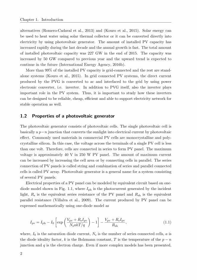
Electrical properties of a PV panel can be modeled by equivalent circuit based on one-
diode model shown in Fig. 1.1, where Iph is the photocurrent generated by the incident
light, Rs is the equivalent series resistance of the PV panel and Rsh is the equivalent
parallel resistance (Villalva et al., 2009). The current produced by PV panel can be
expressed mathematically using one-diode model as
Ipv = Iph − I0
[
exp
(
Vpv +RsIpvNsakT/q
)
− 1
]
− Vpv +RsIpvRsh
, (1.1)
where, I0 is the saturation diode current, Ns is the number of series connected cells, a is
the diode ideality factor, k is the Bolzmann constant, T is the temperature of the p− n
junction and q is the electron charge. Even if more complex models has been presented,
2

1.2. Properties of a photovoltaic generator
one-diode model offers good compromise between accuracy and complexity.
phIdI
pvV
pvIsR
shR
Fig. 1.1: The equivalent circuit of a PV panel based on one-diode model.
When Ipv is zero, PV panel operates in open-circuit (OC) condition. Respectively,
when the voltage Vpv is zero, PV panel operates in short-circuit (SC) condition. In
both of these conditions, the output power of the PV model is zero. The output power
is maximized at a certain operating point called maximum power point (MPP), located
between these conditions. The dependency of output current, output power and dynamic
resistance on voltage in a typical PV panel is shown in Fig. 1.2. As the current is almost
constant in the area between the SC condition and MPP, it is called constant current
(CC) region. Correspondingly, the area between MPP and SC condition is called constant
voltage (CV) region. The dynamic resistance represents the low-frequency value of the
PV panel output impedance and can be defined as
rpv = −∆vpv∆ipv
, (1.2)
where the minus sign indicates that the current is flowing out from the PVG. As shown in
Fig. 1.2, the dynamic resistance is nonlinear and dependent on the operating point. At
the MPP, static and dynamic resistances are equal, i.e. rpv = Umpp/Impp = Rpv (Wyatt
and Chua, 1983). In CC region, dynamic resistance is higher than static resistance,
whereas in CV region, dynamic resistance is lower than static resistance.
The current-voltage (IV) curve of a PV panel is shown in Fig. 1.3 for two different
irradiance and ambient temperature levels. As it is shown, the current produced by
the PV panel is linearly dependent on irradiance level and inversely proportional to
temperature. However, the effect of irradiance is much stronger compared to the effect
of temperature level. Correspondingly, the voltage across the PV panel terminals is
inversely proportional to temperature and it is also slightly affected by the irradiance
level. The highest output power is obtained at low temperature and high irradiance
level.
3

Chapter 1. Introduction
0.0 0.2 0.4 0.6 0.8 1.0 1.20.0
0.2
0.4
0.6
0.8
1.0
1.2
Voltage (p.u.)
Curr
ent,
pow
er a
nd r
esis
tance
(p.u
.)
pvIpvP
pvr
CC CV
MPP
Fig. 1.2: Typical IV curve and dynamic resistance of a PV panel.
0.0 0.2 0.4 0.6 0.8 1.0 1.2 1.4 1.60.0
0.2
0.4
0.6
0.8
1.0
1.2
1.4
1.6
Voltage (p.u.)
Curr
ent
(p.u
.)
1400
1000
2W/m
2W/m
C°251.9 C°
Fig. 1.3: The effect of temperature and irradiance on IV curve of a PV panel.
Manufacturers of PV panels provide values of OC voltage, SC current, MPP voltage
and MPP current in the datasheet of the panel. These values are measured in Standard
Test Condition (STC), i.e. when the irradiance is 1000 W/m2 and the ambient temper-
ature is 25 C. However, the ambient temperature is usually higher and the irradiance is
varying due to the passing clouds. In addition, the irradiance can be reflected from the
clouds yielding as high irradiance as 1400 W/m2 at the surface of the PV panel (Luoma
et al., 2012). This phenomenon is known as cloud enhancement. The maximum value of
the produced current and power together with the maximum voltage must be taken into
4

1.2. Properties of a photovoltaic generator
account in the design of the interfacing converter.
In addition to temperature and voltage, also the distribution of solar irradiance on a
PV generator surface affects heavily the IV curve and maximum output power of the PV
generator. The surface can be shaded partially or entirely e.g. by clouds, buildings and
trees. In order to prevent heating of shaded cells by the non-shaded cells, manufacturers
add so called bypass diodes antiparallel of group of cells. Typically, the size of the cell
group is around 20 cells yielding three bypass diodes in 190 W PV panel. In this kind
of PV panel, three separate maximum power points can occur if the irradiance level is
different for each group.
The MPP locates at the lowest voltage level, when two out of three cell groups are
shaded. This situation is shown in Fig. 1.4, where the output current (solid line) and
power (dashed line) are shown as functions of voltage. The irradiance of the non-shaded
cell is 1000 W/m2 and 100 W/m2 for the shaded cells. In this situation, the voltage
of the MPP is one third of the MPP voltage in non-shaded condition. If the maximum
power is to be extracted also in this situation, the input voltage range of the interfacing
converter should be wide, as it should be able to handle also the maximum OC voltage
of the PVG.
0.0 0.2 0.4 0.6 0.8 1.0 1.2 1.40.0
0.2
0.4
0.6
0.8
1.0
1.2
Voltage (p.u.)
Curr
ent
and p
ow
er (
p.u
.)
MPP1
MPP2pvP
pvI
Fig. 1.4: The effect of partial shading on IV curve of a PV panel.
As the location of the MPP is constantly varying, the operating point of the interfacing
converter must be changed as well in order to extract maximum power from the PVG.
Various maximum power point tracking (MPPT) algorithms have been developed for
this purpose (Esram and Chapman, 2007). Perturb & Observe (P&O) is simple and one
of the most widely used methods, where the operation point is changed in small steps.
5
Chapter 1. Introduction
If the power level was increased, second step is made to the same direction, but if the
power level was decreased, the direction of the step is changed. One of the drawbacks
of this algorithm is that it can locate only local MPP but fails to locate global MPP.
For example, if the P&O algorithm starts from OC voltage in Fig. 1.4, it goes to lower
voltage levels step-by-step. Once it obtains MPP2, it starts to oscillate around it and
will not go down to MPP1 even if the power level would be higher. For this reason, also
algorithms for tracking the global MPP has been developed (Boztepe et al., 2014).
1.3 Grid-connected PV power plant concepts
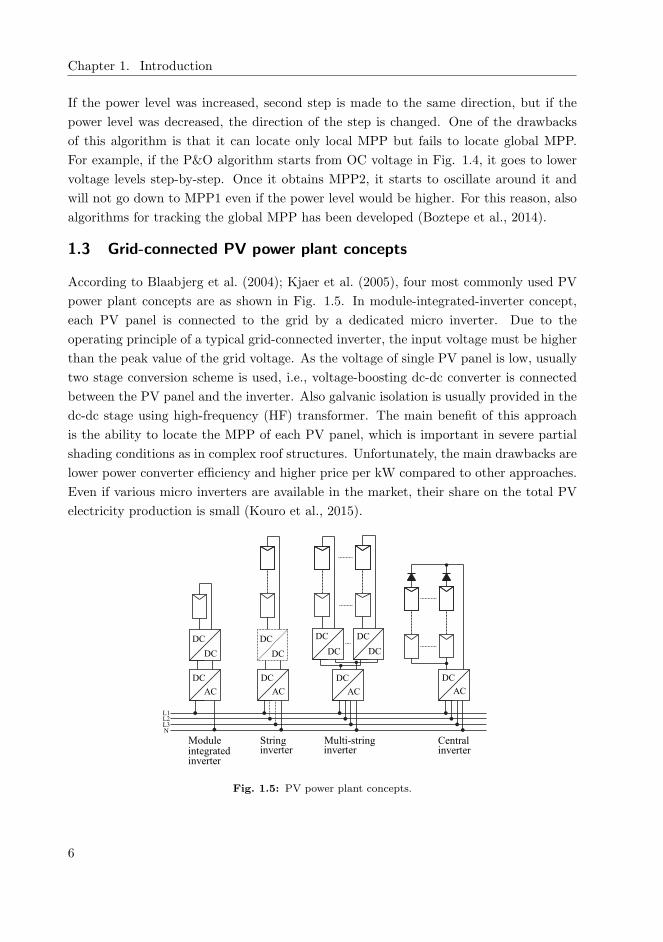
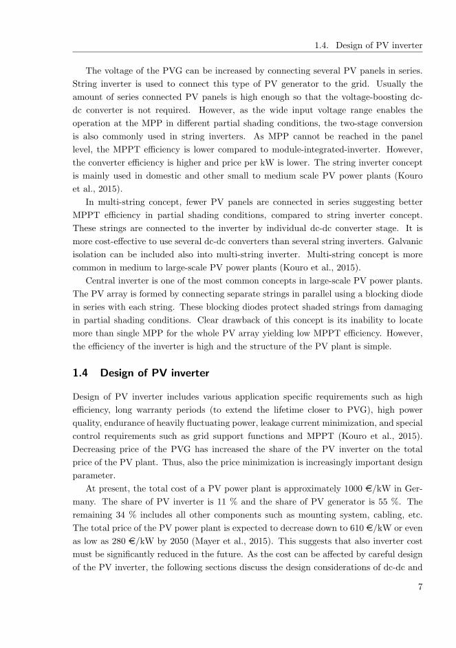
According to Blaabjerg et al. (2004); Kjaer et al. (2005), four most commonly used PV
power plant concepts are as shown in Fig. 1.5. In module-integrated-inverter concept,
each PV panel is connected to the grid by a dedicated micro inverter. Due to the
operating principle of a typical grid-connected inverter, the input voltage must be higher
than the peak value of the grid voltage. As the voltage of single PV panel is low, usually
two stage conversion scheme is used, i.e., voltage-boosting dc-dc converter is connected
between the PV panel and the inverter. Also galvanic isolation is usually provided in the
dc-dc stage using high-frequency (HF) transformer. The main benefit of this approach
is the ability to locate the MPP of each PV panel, which is important in severe partial
shading conditions as in complex roof structures. Unfortunately, the main drawbacks are
lower power converter efficiency and higher price per kW compared to other approaches.
Even if various micro inverters are available in the market, their share on the total PV
electricity production is small (Kouro et al., 2015).
AC
DC
DC
DC
AC AC AC
DC DC
DC
DC DC
DC
DC
L1L2L3N
Moduleintegratedinverter
Stringinverter inverter
Multi-stringinverterCentral
DC
DC
Fig. 1.5: PV power plant concepts.
6
1.4. Design of PV inverter
The voltage of the PVG can be increased by connecting several PV panels in series.
String inverter is used to connect this type of PV generator to the grid. Usually the
amount of series connected PV panels is high enough so that the voltage-boosting dc-
dc converter is not required. However, as the wide input voltage range enables the
operation at the MPP in different partial shading conditions, the two-stage conversion
is also commonly used in string inverters. As MPP cannot be reached in the panel
level, the MPPT efficiency is lower compared to module-integrated-inverter. However,
the converter efficiency is higher and price per kW is lower. The string inverter concept
is mainly used in domestic and other small to medium scale PV power plants (Kouro
et al., 2015).
In multi-string concept, fewer PV panels are connected in series suggesting better
MPPT efficiency in partial shading conditions, compared to string inverter concept.
These strings are connected to the inverter by individual dc-dc converter stage. It is
more cost-effective to use several dc-dc converters than several string inverters. Galvanic
isolation can be included also into multi-string inverter. Multi-string concept is more
common in medium to large-scale PV power plants (Kouro et al., 2015).
Central inverter is one of the most common concepts in large-scale PV power plants.
The PV array is formed by connecting separate strings in parallel using a blocking diode
in series with each string. These blocking diodes protect shaded strings from damaging
in partial shading conditions. Clear drawback of this concept is its inability to locate
more than single MPP for the whole PV array yielding low MPPT efficiency. However,
the efficiency of the inverter is high and the structure of the PV plant is simple.
1.4 Design of PV inverter
Design of PV inverter includes various application specific requirements such as high
efficiency, long warranty periods (to extend the lifetime closer to PVG), high power
quality, endurance of heavily fluctuating power, leakage current minimization, and special
control requirements such as grid support functions and MPPT (Kouro et al., 2015).
Decreasing price of the PVG has increased the share of the PV inverter on the total
price of the PV plant. Thus, also the price minimization is increasingly important design
parameter.
At present, the total cost of a PV power plant is approximately 1000 e/kW in Ger-
many. The share of PV inverter is 11 % and the share of PV generator is 55 %. The
remaining 34 % includes all other components such as mounting system, cabling, etc.
The total price of the PV power plant is expected to decrease down to 610 e/kW or even
as low as 280 e/kW by 2050 (Mayer et al., 2015). This suggests that also inverter cost
must be significantly reduced in the future. As the cost can be affected by careful design
of the PV inverter, the following sections discuss the design considerations of dc-dc and
7
Chapter 1. Introduction
dc-ac converters in PV application.
1.4.1 Design considerations of dc-dc converter in PV application
As it was mentioned earlier, addition of dc-dc converter between the PVG and the dc-
ac inverter increases the input voltage range of the PV inverter. When considering
conventional MPPT operation, the main benefit is increased MPP range. It is also
beneficial to implement the galvanic isolation in the dc-dc converter if such property is
required in the local grid code. As the share of the electricity produced by PV power
plants increases, it becomes more important to implement grid-supporting functions in
the PV inverters. One of these functions is the ability to limit the output power of
the PV inverter. This means that instead of MPP operation, the inverter is limiting
the output power referred to as a constant power generation (CPG). In order to obtain
CPG in varying environmental conditions, two stage conversion might be compulsory
(Cai et al., 2016; Sangwongwanich et al., 2016; Tonkoski et al., 2011; Yang et al., 2014).
Moreover, bidirectional dc-dc converters are required in grid-connected energy storage
systems (ESS) (Grainger et al., 2014). Due to the aforementioned reasons, using of double
stage conversion in future PV inverters seems essential. Thus, main focus of this thesis
is on the control design and component sizing of dc-dc converters in PV application.
Typically the PVG and the power electronic devices are purchased from different
manufacturers. The required number of PV panels is calculated by dividing the target
power level of the PV plant by the STC power provided in the panel datasheet. The
power electronic devices are further selected based on the STC power of the PVG. It
must also be checked that the maximum input current of the PV inverter is high enough
and the input voltage range is suitable for the PVG. The relation between the STC power
of the PVG PPV,STC and the nominal power of the inverter Pinv,nom can be described by
the dc-ac ratio or by its inverse, the sizing ratio SR:
SR =Pinv,nom
Ppv,stc, (1.3)
The optimal value of sizing ratio is extensively studied in the literature (Burger and
Ruther, 2006; Chen et al., 2011, 2013; Koutroulis and Blaabjerg, 2011; Luoma et al.,
2012; Mondol et al., 2006; Notton et al., 2010; Sulaiman et al., 2012; Tonkoski and
Lopes, 2011; Zhu et al., 2011). The optimal value depends on the location of the PV
plant, government incentives, inverter power efficiency curve, inverter protection scheme,
cost of the PV panels and inverters, cloud shading conditions, etc. (Chen et al., 2011;
Luoma et al., 2012). The optimum value of the sizing ratio in the range of 0.6-1.5 has
been suggested.
8

1.4. Design of PV inverter
As the PV inverter is not usually designed for a specific PVG, the inverter manu-
facturers aim to design the inverter as generally applicable as possible. Therefore, the
input current of the inverter is usually calculated by diving the nominal power of the con-
verter by the minimum input voltage (Datasheet of ABB string inverter PRO-33.0, 2016;
Datasheet of Sunny Tripower 10000TLEE-JP, 2016; Datasheet of Vacon 8000 solar in-
verter series, 2014). This is also the case in (Ho et al., 2013, 2012), where the interleaved
voltage-boosting converter was designed for PV application. By dividing the nominal
power by the minimum input voltage it is guaranteed that the nominal power can be
handled over the whole input voltage range. However, as the source is PVG, the power is
maximized at higher than the minimum voltage. This design method yields reasonable
design when the input voltage range is narrow. However, it yields oversized components
and uneven temperature distribution if used for designing PV inverter having wide input
voltage range, as shown in Chapter 2.
Single-phase PV inverters are used in small-scale residential string inverters and in
micro inverters as it was shown in Fig. 1.5. The grid current and voltage are both
fluctuating at the grid frequency. When assuming unity power factor, the output power
of a single phase inverter is fluctuating at twice the grid frequency. This power fluctuation
causes voltage ripple in the dc-link voltage and the PVG voltage. However, the PVG
voltage should be as constant as possible to maximize the energy yield (Sullivan et al.,
2013) and maintain stable operation of the MPPT (Femia et al., 2009). The low-frequency
ripple causes problems also in lightning and fuel-cell applications, when single-phase
inverter is used (Sun et al., 2016). Various solutions has been presented to prevent
output power ripple from affecting the input power, i.e. to implement power decoupling
(Hu et al., 2013; Sun et al., 2016; Tang and Blaabjerg, 2015).
In case of two stage conversion scheme, a large capacitor can be connected in parallel
to the PVG or the dc-link capacitance can be increased to produce power decoupling. As
the dc-link voltage level is higher than the PVG voltage, the same amount of capacitance
produces stronger power decoupling, when added to the dc-link instead of adding it par-
allel to the PVG. As large capacitor parallel to the PVG also limits the control bandwidth
of the input voltage controlled dc-dc converter, increasing the dc-link capacitance is the
best of these two passive power-decoupling options.
The dc-link voltage ripple is inversely proportional to the capacitance value of the
dc-link capacitor. Minimized capacitance value is desired, as the reliability could be
improved if electrolytic capacitors could be replaced by film or other type of capacitors.
It is possible to use relatively small capacitor yielding high ripple if the ripple is prevented
from affecting the PVG voltage. This ripple-rejection capability can be obtained by using
input-voltage control in the dc-dc converter. It has been shown that the double-line
frequency ripple can be attenuated by using simple I-type controller (Viinamaki et al.,
9

Chapter 1. Introduction
2014), high bandwidth PI controller together with quasi-resonant controller (Gu et al.,
2014) or high bandwidth PID controller (Femia et al., 2009). High-bandwidth input-
voltage control enables also faster MPPT, yielding higher MPPT efficiency compared to
open-loop operation. Despite these advantages, the open-loop operation is still widely
used. The reasons for its popularity might be simplicity and lower risk for instability as
there are no feedback loops.
The double-line frequency ripple rejection capability can be implemented also in dc-
dc converter operating in open loop by using dc-link voltage feedforward (Mirzahosseini
and Tahami, 2012). Input voltage feedforward has been conventionally used in voltage
sourced dc-dc converters to reduce the magnitude of the audio susceptibility, i.e. input-
to-output transfer function (Kazimierczuk and Starman, 1999; Redl and Sokal, 1986). It
has also been used in PFC boost converters to reduce harmonic components from grid
current (Van De Sype et al., 2005). However, using of feedforward in this application
has not been extensively studied so far. In Chapter 2, small-signal model of conventional
voltage-boosting dc-dc converter including dc-link voltage feedforward is shown. The
presented model is used for studying the factors affecting the maximum attenuation of
double-line frequency voltage ripple.
1.4.2 Selection of passive components in three-phase dc-ac inverter
Two-level three-phase dc-ac inverter is commonly used topology in higher power level
string inverters and central inverters. It consists of switch bridge, input or dc-link ca-
pacitor and grid connection filter. Many studies has been carried out on sizing of dc-link
capacitor and grid connection filter as these passive components are the biggest con-
tributors to the size and cost of the inverter. The minimum capacitance value of the
input capacitor is limited by the maximum allowable voltage ripple and the stability of
the control loop. In (Messo et al., 2014), design rules were presented for the minimum
dc-link capacitance, when considering the stable operation of the PV inverter.
In grid-connected PV inverters, LCL-type grid filter is typically used. It offers the
same attenuation capability in smaller size compared to L-type filter, which was popular
in traditional grid-connected inverters. The selection of the optimum capacitance and
inductance values of the LCL-type grid filter has been studied in (Beres et al., 2016;
Channegowda and John, 2010; Karshenas and Saghafi, 2006; Lang et al., 2005; Liserre
et al., 2004, 2005; Muhlethaler et al., 2013; Pan et al., 2014; Zheng et al., 2013). In (Pan
et al., 2014), the focus was on the inductor design and it was shown how the core material
can be saved by combining the cores of the filter inductors. In (Muhlethaler et al., 2013),
it was shown how the optimal LCL-filter design is a compromise between the losses and
filter size.
Using of soft-saturating core materials without discrete air gap or by minimizing the
10

1.4. Design of PV inverter
core size yield an inductor, which will saturate during the grid period. The inductance of
the saturating inductor is current dependent, whereas in linear inductor the inductance
is approximately constant. Given that the cost and size of PV inverter must be further
reduced and using of saturating inductors might help to obtain this target, it is important
to study the effect of saturating filter inductors on the performance of the PV inverter.
The effect of saturation and hysteresis can be investigated by the Jiles-Atherton model
(Liu et al., 2012; Ngo, 2002; Sadowski et al., 2002). If the target is to model only the in-
ductor saturation and the inclusion of hysteresis does not provide any useful information,
the effect of hysteresis can be neglected. In this case, a simple behavioral model can be
used (Perdigao et al., 2008; Wolfle and Hurley, 2003). The Jiles-Atherton model is based
on the physical properties of the core material, whereas the behavioral model is based on
the measured properties of the inductor. In (Di Capua and Femia, 2016), a behavioral
model including inductor saturation and temperature dependency was developed. It was
also demonstrated that this model predicts the switching-frequency current ripple of the
dc-dc converter correctly.
The modeling and simulation of saturated induction motors is widely studied in the
literature. An extensive literature review on these models is given in (Nandi, 2004). It
also proposes a new model for predicting the low-frequency current harmonics produced
by the saturation in induction motor aiming to fault analysis. Most of the presented
models are also based on measured parameters and are rather behavioral than physical
models. For example in (Donescu et al., 1999), the dependency of magnetizing inductance
on stator flux was measured in three operating points and the mathematical represen-
tation was fitted to the measured data. As the simplified equivalent circuit of induction
motor resembles the grid-connected PV inverter, some of the results observed in the op-
eration of saturating induction motors might be valid also for the PV inverter. However,
these similarities might not be easy to observe due to the complexity of the motor model.
Mastromauro et al. studied the effect of saturating inductor in the L-filter of a grid-
connected single-phase inverter and explained by Volterra theory that applying 50 Hz
sinusoidal voltage across the saturating inductor produces third and fifth harmonics to
the current (Mastromauro et al., 2008). Moreover, the presence of third harmonic volt-
age produces third, ninth and fifteenth harmonic currents. If both of these components
are applied at the same time, intermodulation components are also produced. Further-
more, Wolfe and Hurley explained through Fourier analysis that the saturating inductor
produces odd harmonics (Wolfle and Hurley, 2003). In (Mastromauro et al., 2008), it
was also shown that in case of single-phase inverter, the harmonics caused by inductor
saturation can be effectively attenuated using resonant or repetitive controllers.
In Chapter 4, the effect of saturating L-filter inductor on the low-frequency current
harmonics of three-phase PV inverter is studied by simulations and experimental mea-
11

Chapter 1. Introduction
surements. Also an equation for approximating the switching-frequency ripple of the
L-filter inductor is developed. The developed equation can be used for studying the rip-
ple in case of saturating inductors having different inductance-current (LI) dependency.
1.5 Grid-feeding, grid-forming and grid-supporting operation modes
of PV inverter
At present, the PV inverters connected to low-voltage grid are usually required to operate
at unity power factor (PF) and to operate at the MPP. Furthermore, the inverter is
disconnected in case of grid fault. These requirements are determined in the grid code
locally. As the share of renewable energy sources on the total electricity production
increases, shutting down several distributed generation (DG) plants simultaneously will
have severe effect on the grid stability. Other well known issue of the renewable energy
sources is the intermittent nature, which will also affect the grid stability due to the power
imbalance. In order to ensure reliable operation of the grid, various improvements have
been suggested to the current grid codes and some of them has already been executed in
countries having high penetration of renewable energy (Yang et al., 2015).
In Germany, the PV power plants having rated power below 30 kWp have to be able
to limit the maximum feed-in power (e.g. 70% of the rated power). This means that
the inverter has to be able to operate in power limiting mode called constant power
generation (CPG) in addition to MPPT. This operation is also described in the Danish
grid code (Sangwongwanich et al., 2016). The aim is to improve the power balance of
the grid by cutting the highest peaks from the feed-in power. These peaks could also be
handled by using energy storage systems (ESS), but their extensive use would require
cheaper and more reliable ways to store energy. Thus, CPG is seen as good method to
avoid the use of ESS at the moment.
Several countries have also requirement to feed reactive power to the grid by the PV
inverter in case of voltage sag in medium- and high-voltage grids. This property is known
as low-voltage-ride-through (LVRT) capability (Neves et al., 2016). In (Yang et al., 2015)
it was suggested that LVRT requirement should be applied also for low-voltage grid.
When the PV inverter is performing some of these grid-supporting functions, it is said
to operate in grid-supporting mode.
When the PV inverter is feeding power to the grid at unity power factor and operates
at the MPP, it is said to operate in grid-feeding mode. In grid-feeding operation, the
inner control loop of the inverter controls the grid current. The q-component reference
is set to zero for unity power factor, and the d-component reference is determined by
the dc-link voltage controller. In case of two-stage conversion, dc-dc converter controls
the PVG voltage and the reference value is given by the MPPT. In case of single-stage
conversion, the outer control loop of the inverter is controlling the PVG voltage instead
12

1.5. Grid-feeding, grid-forming and grid-supporting operation modes of PV inverter
of the dc-link voltage. The control scheme is basically similar in grid-support operation.
However, in this case, the grid current q-component can be controlled to increase the
grid voltage or the MPPT can be disabled and the reference value of the PVG voltage
controller can be determined, e.g., by CPG function.
The purpose of LVRT is to support the grid during a short-term voltage sag. If the grid
voltage drops down for longer period, the inverter must be disconnected from the grid for
safety reasons according to majority of current grid codes. This might be changed in the
future, when the microgrid vision will turn into reality (Mastromauro, 2014). Microgrid
refers to a small-scale network composed of distributed power generation as PV and wind
power plants, ESSs and consumers. The communication between the parts of microgrid is
much heavier than in current grid enabling the stable operation of the grid even without
large large-scale power plants such as nuclear etc. (Bacha et al., 2015; Rocabert et al.,
2012; Wang et al., 2015). In microgrid, the grid-connected PV inverter can operate either
in grid-feeding, grid-supporting or grid-forming operation modes (Rocabert et al., 2012).
In grid-forming operation, the inverter will determine the grid voltage. In case of double-
stage PV inverter, the dc-link voltage is determined by the dc-dc converter. The power
fed to the grid is determined by the local load, suggesting that MPPT cannot be used.
In addition to microgrid, some grid codes allow the grid-forming operation already in
small-scale (islanding), under condition that the islanded grid is isolated from the grid
(Bacha et al., 2015).
In ESS, where a dc-dc converter is connected between PVG and a battery, the con-
verter must be able to operate in MPPT mode, when the voltage of the battery is below
the set limit. After the voltage exceeds this limit, operation mode is changed to constant
voltage charging. This means that the converter must be able to quickly change between
MPPT mode and output voltage control mode (Qin et al., 2015). The control problem
is the same for dc-dc converter in two-stage PV inverter, which must be able to operate
in grid-feeding and grid-forming operation modes. According to previous discussion, it
is important to understand how the operation in both of these modes affects the control
design and component selection of the converter.
When operating in MPPT mode, the dc-dc converter can operate either in open
loop or in closed loop. If the converter is operating in open loop, the tracker speed
must be small. Using closed loop operation, higher speed and better MPPT efficiency
can be obtained. In case of open-loop operation, the output of the MPPT is duty
cycle. Respectively, when the converter is operating in closed loop, the PVG voltage is
controlled and the output of the MPPT is the PVG voltage reference. The voltage of
the PVG is usually controlled instead of the current as the rate of change is much bigger
in current than in voltage. This means that the PVG must be modeled as a current
source in this case. As the source in conventional applications has usually been voltage
13

Chapter 1. Introduction
source, also PVG is still often modeled as a voltage source (Danyali et al., 2014; Villalva
et al., 2010). However, also publications where the current source is used, are presented
(Messo et al., 2012; Urtasun et al., 2013). In this thesis, the combined dynamics of the
voltage-boosting converter and PVG is presented, and the developed small-signal model
is used for analyzing the effect of dc-link voltage feedforward and input voltage control
on double-line-frequency ripple attenuation.
The small-signal model of the voltage-boosting converter is different when the con-
verter controls the dc-link voltage. Contrary to the input voltage control, the converter
can be designed for stable operation only in CC or in CV region. In (Konstantopoulos
and Alexandridis, 2013), nonlinear voltage regulator was used to solve this problem. In
(Qin et al., 2015), the stability of output-voltage-controlled voltage-boosting converter
was studied and it was verified that the converter cannot be stable in both of these re-
gions with the same controller. However, explanation was not provided for this behavior.
In Chapter 3 of this thesis, the small-signal model of output-voltage-controlled voltage-
boosting converter is presented by modeling the PVG as current source and as voltage
source. The difference between these models are explained. Using the developed models,
the limiting factors affecting the control design and component selection are shown.
1.6 The objectives of the thesis
The aim was to study the component selection and control design of voltage-boosting
dc-dc converter operating as a part of two-stage single-phase PV inverter. Operation in
grid-feeding and grid-forming modes were both studied. In case of grid-feeding operation,
the attenuation of double-line-frequency voltage ripple from the dc-link voltage to the
voltage of the PVG was taken into account in the control design. During the studies, it
was realized that this attenuation can be improved by adding dc-link voltage feedforward
to the converter. Thus, one of the set targets was to find out the factors affecting the
maximum available attenuation of double-line-frequency voltage ripple when using dc-
link voltage feedforward. Finally, the effect of using saturating grid filter inductors in
the grid-connected three-phase PV inverter on low-frequency and switching-frequency
harmonics was studied. The intention was to find out if the low-frequency harmonics
would be too high to be attenuated by the conventional control methods. Also, as the
varying inductance in saturating grid filter inductors is never in their minimum value at
the same time in all the three phases, it was considered if the three-phase inverter would
offer any benefit over the single-phase inverter, when the saturating inductors are used.
1.7 Main scientific contributions
The main scientific contributions of this thesis can be summarized as
14
1.8. Related publications and author’s contribution
• The dynamic model of voltage-boosting dc-dc converter operating as a part of two-
stage PV inverter is developed. Grid-feeding and grid-forming modes are both
studied. When the inverter is operating in grid-forming mode, the dc-dc converter
controls the dc-link voltage. It is explained, why the same controller cannot be used
in the whole operating range of the PV generator. It is shown that the low-frequency
RHP zero occurring in current region limits the bandwidth of the controller to a
low value. High-bandwidth controller can be used only in voltage region. However,
if the PV generator operating point goes from voltage region to current region,
the voltage will collapse and the controller will not recover. Contrary to this, the
current region controller is able to recover from the unstable region if the operating
point enters into voltage region and back.
• It is shown that taking into account the properties of a PV generator, when design-
ing a voltage-boosting dc-dc converter, yields smaller inductor size, smaller input
capacitor and smaller heat sink compared to the conventional method, when the
input voltage range of the converter is wide.
• The small-signal model is developed and used to study the attenuation of double-
line-frequency voltage ripple in the voltage-boosting dc-dc converter using dc-link
voltage feedforward and operating the converter in open loop. It is shown that the
maximum attenuation is obtained by using as high dc-link voltage as possible, as
small measurement error as possible, and by ensuring that the losses between the
upper and lower switches are as equal as possible.
• Two different simulation models are developed and used to show that the satura-
tion of grid filter inductors in grid-connected three-phase VSI introduces 5th and
7th harmonics to the grid current but they can be effectively attenuated by using
conventional PI controllers in the dq-frame. Also an equation for approximating the
amplitude of switching frequency current ripple in three-phase PV inverter having
saturating grid filter is presented and validated.
1.8 Related publications and author’s contribution
The author made the analysis, designed and built the prototype converters, made the
measurements and was the main author in writing of [P1-P5]. In [P6], the author par-
ticipated in the analysis and made the measurements. Prof. Suntio was supervising
the research documented in [P1-6]. He also introduced valuable ideas and comments
related to the conducted research and was the main author in [P6]. Dr.Tech. Jokipii
helped with the analysis in [P2-P3] and with the proofreading in [P2-P6]. He gave also
valuable support for building the prototype inverter used for the measurements in [P3].
Dr.Tech. Messo participated in the analysis and helped with the measurements in [P5]
15

Chapter 1. Introduction
and [P6]. M.Sc. Kivimaki and M.Sc. Hietalahti helped with the proofreading in [P4].
Prof. Kuperman gave support for writing of [P1], [P5] and [P6].
[P1] Viinamaki, J., Kuperman, A., Suntio, T. (2017). “Grid-forming-mode operation
of boost-power-stage converter in PV-generator-interfacing applications”, Energies,
vol. 10, no. 7, pp. 1–23
[P2] Viinamaki, J., Jokipii, J., Suntio, T. (2016). “Improving double-line-frequency volt-
age ripple rejection capability of DC/DC converter in grid connected two-stage PV
inverter using DC-link voltage feedforward”, in 18th European Conference on Power
Electronics and Applications, EPE’16 ECCE Europe, pp. 1–10
[P3] Viinamaki, J., Jokipii, J., Suntio, T. (2015). “Effect of inductor saturation on
the harmonic currents of grid-connected three-phase VSI in PV application”, in 9th
International Conference on Power Electronics - ECCE Asia, ICPE’16 ECCE Asia,
pp. 1–10
[P4] Viinamaki, J., Kivimaki, J., Suntio, T., Hietalahti, L. (2014). “Design of boost-
power-stage converter for PV generator interfacing”, in 16th European Conference
on Power Electronics and Applications, EPE’14 ECCE Europe, pp. 1–10
[P5] Viinamaki, J., Jokipii, J., Messo, T., Suntio, T., Sitbon, M., Kuperman, A. (2015).“’Com-
prehensive dynamic analysis of photovoltaic generator interfacing DC-DC boost
power stage’, IET Renewable Power Generation, vol. 9, no. 4, pp. 306–314
[P6] Suntio, T., Viinamaki, J., Jokipii, J., Messo, T., Kuperman, A. (2014). “Dynamic
characterization of power electronic interfaces”, IEEE Journal of Emerging and Se-
lected Topics in Power Electronics, vol. 2, no. 4, pp. 949–961
1.9 The structure of the thesis
Chapter 2 focuses on the design of voltage-boosting dc-dc converter operating in grid-
feeding mode. First, the small-signal model of the converter is presented. Next, the
research on the component selection and control design of the converter is presented.
Finally, the factors affecting the maximum attenuation of double-line-frequency voltage
ripple, when using dc-link voltage feedforward are shown. Chapter 3 discusses the design
of voltage-boosting dc-dc converter operating in grid-forming mode. After developing the
small-signal model, the factors affecting the component selection and control design are
presented. Chapter 4 discusses the effects of inductor saturation on the low-frequency and
switching-frequency harmonics of the grid-connected three-phase PV inverter. Finally,
the conclusions and suggested future topics are presented in Chapter 5.
16

2 DESIGN OF VOLTAGE-BOOSTING DC-DC
CONVERTER OF TWO-STAGE PV INVERTER
OPERATING IN GRID-FEEDING MODE
In this chapter, a small-signal model of voltage-boosting dc-dc converter operating as
a part of two-stage PV inverter is developed. The properties of the PVG are taken
into account in the model but the dc-ac inverter is neglected as the focus is on the
dc-dc converter. The developed model is used in selecting the passive components of
the converter as well as for studying the effect of using input-voltage control and dc-link
voltage feedforward for attenuating double-line-frequency voltage ripple, which is present
in single-phase PV inverter.
2.1 Small-signal modeling of switched-mode dc-dc converters
Small-signal model of a dc-dc converter can be developed using state space averaging
method, which was introduced by Middlebrook in 70’s (Cuk and Middlebrook, 1977;
Middlebrook, 1988). In this method, the differential equations describing the averaged
operation of the power circuit over a single switching period are linearized around a
steady state operation point. The obtained model is accurate and valid up to half the
switching frequency. The accuracy and simplicity are probably the main reasons for
this method being so popular for modeling dc-dc converter dynamics. The linearized
differential equations describing the power circuit can be presented in a general state-
space form as
dx(t)
dt= Ax(t) +Bu(t)
y(t) = Cx(t) +Du(t),
(2.1)
where A, B, C, D are constant matrices, u is the input vector, y is the output vector
and x is the state vector. The linearized model can be transformed into the frequency
domain by Laplace transform yielding
17

Chapter 2. Design of voltage-boosting dc-dc converter of two-stage PV inverteroperating in grid-feeding mode
sX(s) = AX(s) +BU(s)
Y (s) = CX(s) +DU(s).(2.2)
The transfer function matrix G describing the relation between the input and output
variables can be solved based on (2.2) as
Y (s) = (C(sI−A)-1B+D)U(s) = GU(s). (2.3)
The inductor current and capacitor voltage are usually selected as state variables.
The duty ratio is considered as control variable. The input variables are determined by
the source and load of the converter. Those variables that do not belong in the above-
mentioned groups are the output variables of the model. Thus, the input and output
variables are application dependent. As shown in Fig. 2.1, four possible load/source con-
figurations can be recognized: Voltage-fed voltage output (VF-VO), voltage-fed current
output (VF-CO), current-fed current output (CF-CO) and current-fed voltage output
(CF-VO) (Suntio, 2009; Suntio et al., 2014). The corresponding transfer function matri-
ces are called G, Y, H, and Z-parameter sets, respectively.
G Y
H Z
a) b)
c) d)
ini
inv
ovoi
ini
invoi
ov
ini
inv
oi
ov
invini
oi
ov
Fig. 2.1: Converter can be a) voltage-fed voltage output (VF-VO), b) voltage-fed current output(VF-CO), c) current-fed current output (CF-CO) and d) current-fed voltage output (CF-VO) .
When considering the VF-VO converter, the input voltage is determined by the volt-
age source and the load current is determined by the current sink. The value of the input
voltage or output current cannot be affected by the duty cycle as they are determined
externally. Thus, these variables are considered as inputs to the model, i.e., input vari-
18
2.2. H-parameter model of voltage-boosting dc-dc converter
ables. Input current and output voltage can be affected by varying the duty cycle or the
input variables, so they are considered as output variables of the model.
G-parameters are used in conventional applications, where the converter is fed from
a constant voltage source and the output voltage of the converter is to be regulated. In
lighting application, the current of Light Emitting Diodes (LEDs) are controlled using dc-
dc converter, which could be modeled using Y-parameter model. H-parameters are used
in PV applications, where the PV generator voltage is to be controlled and the output
voltage is determined by the battery or by the dc-ac inverter. Finally, Z-parameters can
be used, when the PV interfacing converter is operating in grid-feeding mode, i.e., the
dc-link voltage is controlled by the dc-dc converter instead of the dc-ac inverter.
2.2 H-parameter model of voltage-boosting dc-dc converter
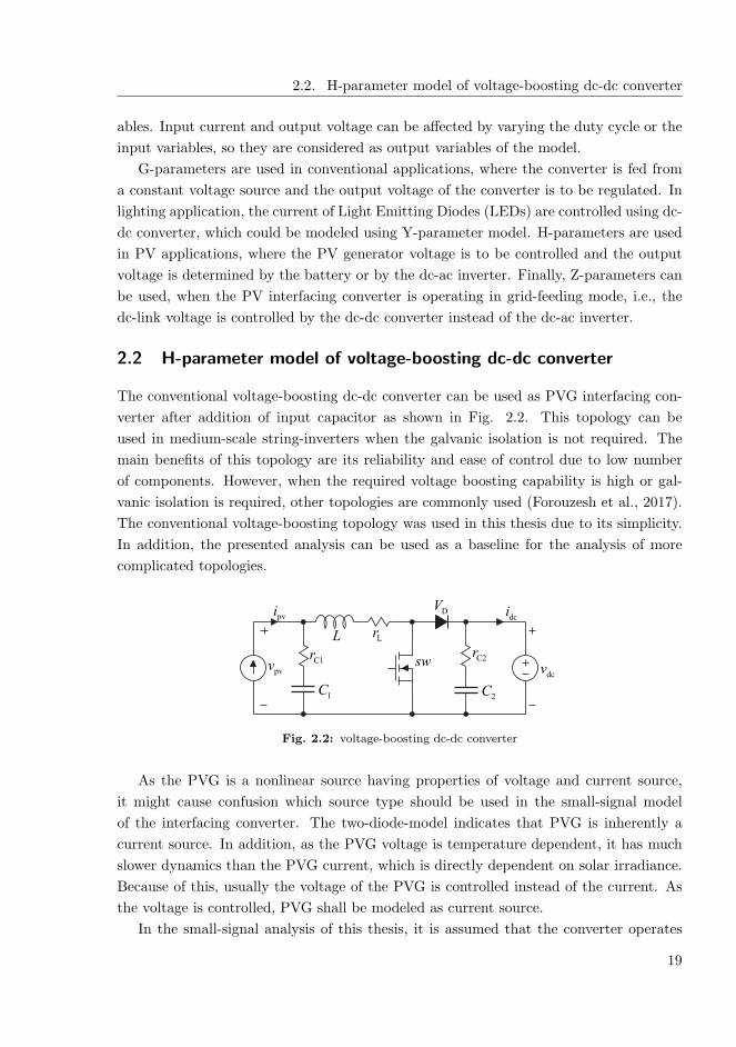
The conventional voltage-boosting dc-dc converter can be used as PVG interfacing con-
verter after addition of input capacitor as shown in Fig. 2.2. This topology can be
used in medium-scale string-inverters when the galvanic isolation is not required. The
main benefits of this topology are its reliability and ease of control due to low number
of components. However, when the required voltage boosting capability is high or gal-
vanic isolation is required, other topologies are commonly used (Forouzesh et al., 2017).
The conventional voltage-boosting topology was used in this thesis due to its simplicity.
In addition, the presented analysis can be used as a baseline for the analysis of more
complicated topologies.
pvi
1C
L
sw
2C
dcv
dci
pvv
Lr
C2rC1r
DV
Fig. 2.2: voltage-boosting dc-dc converter
As the PVG is a nonlinear source having properties of voltage and current source,
it might cause confusion which source type should be used in the small-signal model
of the interfacing converter. The two-diode-model indicates that PVG is inherently a
current source. In addition, as the PVG voltage is temperature dependent, it has much
slower dynamics than the PVG current, which is directly dependent on solar irradiance.
Because of this, usually the voltage of the PVG is controlled instead of the current. As
the voltage is controlled, PVG shall be modeled as current source.
In the small-signal analysis of this thesis, it is assumed that the converter operates
19
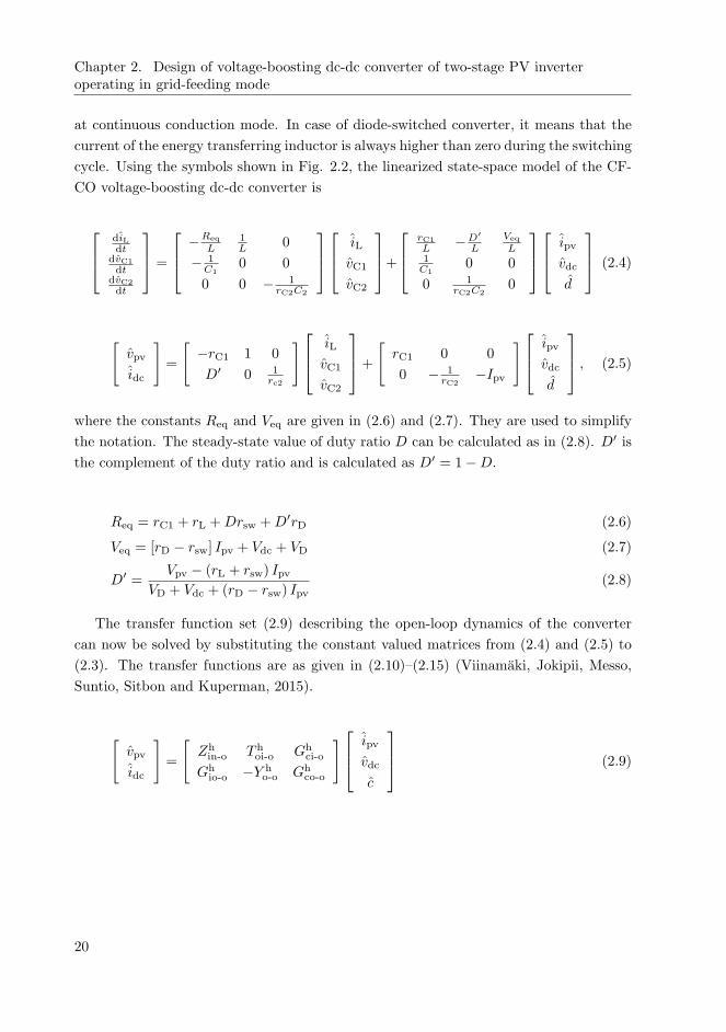
Chapter 2. Design of voltage-boosting dc-dc converter of two-stage PV inverteroperating in grid-feeding mode
at continuous conduction mode. In case of diode-switched converter, it means that the
current of the energy transferring inductor is always higher than zero during the switching
cycle. Using the symbols shown in Fig. 2.2, the linearized state-space model of the CF-
CO voltage-boosting dc-dc converter is
diLdt
dvC1
dtdvC2
dt
=
−Req
L
1L
0
− 1C1
0 0
0 0 − 1rC2C2
iL
vC1
vC2
+
rC1
L−D
′
L
Veq
L
1C1
0 0
0 1rC2C2
0
ipv
vdc
d
(2.4)
[
vpv
idc
]
=
[
−rC1 1 0
D′ 0 1rc2
]
iL
vC1
vC2
+
[
rC1 0 0
0 − 1rC2
−Ipv
]
ipv
vdc
d
, (2.5)
where the constants Req and Veq are given in (2.6) and (2.7). They are used to simplify
the notation. The steady-state value of duty ratio D can be calculated as in (2.8). D′ is
the complement of the duty ratio and is calculated as D′ = 1−D.
Req = rC1 + rL +Drsw +D′rD (2.6)
Veq = [rD − rsw] Ipv + Vdc + VD (2.7)
D′ =Vpv − (rL + rsw) Ipv
VD + Vdc + (rD − rsw) Ipv(2.8)
The transfer function set (2.9) describing the open-loop dynamics of the converter
can now be solved by substituting the constant valued matrices from (2.4) and (2.5) to
(2.3). The transfer functions are as given in (2.10)–(2.15) (Viinamaki, Jokipii, Messo,
Suntio, Sitbon and Kuperman, 2015).
[
vpv
idc
]
=
[
Zhin-o T h
oi-o Ghci-o
Ghio-o −Y h
o-o Ghco-o
]
ipv
vdc
c
(2.9)
20

2.2. H-parameter model of voltage-boosting dc-dc converter
Zhin-o =
1
∆
(Req − rC1 + sL) (1 + srC1C1)
LC1(2.10)
T hoi-o =
1
∆
D′ (1 + srC1C1)
LC1(2.11)
Ghci-o = − 1
∆
Veq (1 + srC1C1)
LC1(2.12)
Ghio-o =
1
∆
D′ (1 + srC1C1)
LC1(2.13)
Y ho-o =
D’2s
∆L+
sC2
1 + srC2C2(2.14)
Ghco-o = −Ipv
∆
(
s2 − s
(
D′Veq
IpvL− Req
L
)
+1
LC1
)
, (2.15)
where ∆ is the denominator of the transfer functions and is given in (2.16). Roots of the
denominator are the poles of the system and the number of the poles equals the degree
of the system.
∆ = s2 + sReq
L+
1
LC1(2.16)
Ideal source and load are assumed in the presented small signal model. However, if
the effect of the finite source or load impedance on the converter dynamics is of interest,
they can be added to the model. In PV application, the output impedance of the PVG
has significant effect on the dynamics of the converter suggesting that its effect shall
be taken into account. The source-affected transfer functions are given in Appendix A.
They are calculated by first adding the source admittance YS to the model as shown in
Fig. A.1. Then, the input current is solved as ipv = ipvS − YSvpv and it is substituted
into (2.9).
The block diagram of the small-signal model of the converter operating under input-
voltage control is presented for the input terminal in Fig. 2.3a and for the output terminal
in Fig. 2.3b. Ghse-in is the measurement gain, Ga is the modulator gain and Gc is the
transfer function of the controller. When the controller is implemented digitally, e.g.,
by using Digital Signal Processor (DSP), the modulator and measurement gains can be
manipulated to unity in in the code. However, as the measurement is usually filtered,
its effect can be taken into account by including the filter pole into the measurement
gain. The blocks inside the dashed line describe the dynamic model of the converter in
open loop. The transfer function set describing the closed-loop small-signal model of the
CF-CO converter is shown in Appedix A
21
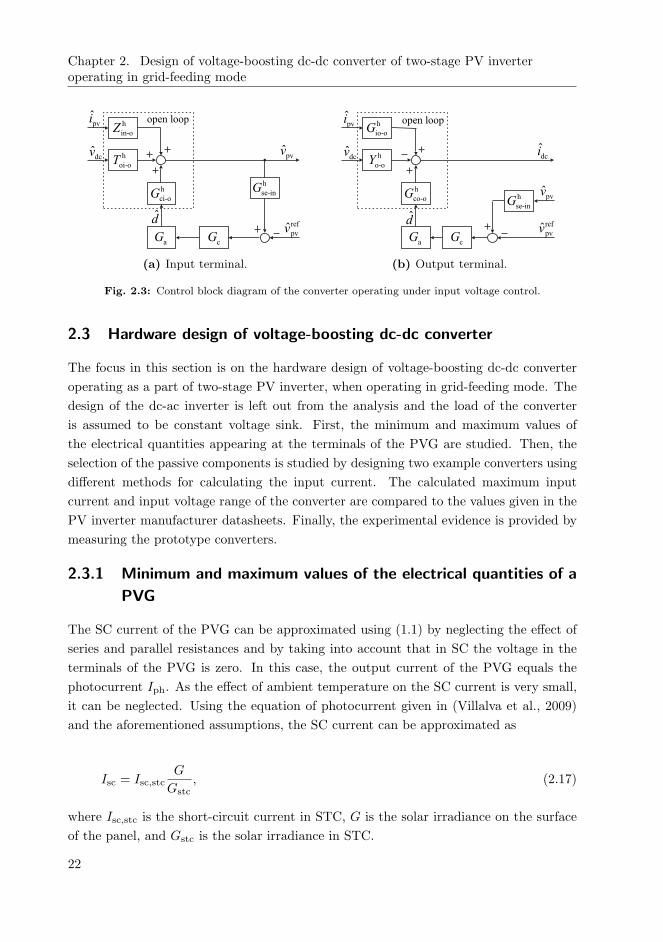
Chapter 2. Design of voltage-boosting dc-dc converter of two-stage PV inverteroperating in grid-feeding mode
h
in-oZ
h
oi-oT
h
ci-oG
aG cG
h
se-inG
pvi
dcv pvv
ref
pvvd
open loop
(a) Input terminal.
h
io-oG
h
o-oY
h
co-oG
aG cG
h
se-inG
pvi
dcv dci
ref
pvvd
pvv
open loop
(b) Output terminal.
Fig. 2.3: Control block diagram of the converter operating under input voltage control.
2.3 Hardware design of voltage-boosting dc-dc converter
The focus in this section is on the hardware design of voltage-boosting dc-dc converter
operating as a part of two-stage PV inverter, when operating in grid-feeding mode. The
design of the dc-ac inverter is left out from the analysis and the load of the converter
is assumed to be constant voltage sink. First, the minimum and maximum values of
the electrical quantities appearing at the terminals of the PVG are studied. Then, the
selection of the passive components is studied by designing two example converters using
different methods for calculating the input current. The calculated maximum input
current and input voltage range of the converter are compared to the values given in the
PV inverter manufacturer datasheets. Finally, the experimental evidence is provided by
measuring the prototype converters.
2.3.1 Minimum and maximum values of the electrical quantities of a
PVG
The SC current of the PVG can be approximated using (1.1) by neglecting the effect of
series and parallel resistances and by taking into account that in SC the voltage in the
terminals of the PVG is zero. In this case, the output current of the PVG equals the
photocurrent Iph. As the effect of ambient temperature on the SC current is very small,
it can be neglected. Using the equation of photocurrent given in (Villalva et al., 2009)
and the aforementioned assumptions, the SC current can be approximated as
Isc = Isc,stcG
Gstc, (2.17)
where Isc,stc is the short-circuit current in STC, G is the solar irradiance on the surface
of the panel, and Gstc is the solar irradiance in STC.
22
2.3. Hardware design of voltage-boosting dc-dc converter
The OC voltage of the PVG can be approximated by using (1.1) by neglecting the
effect of series and parallel resistances, the dependency of short-circuit current on tem-
perature, and by recognizing that the current Ipv is zero at OC condition yielding
Voc = ln
(
GIsc,stcGstcI0
+ 1
)
NsakT
q. (2.18)
As the temperature T is in the numerator of (2.18), it might seem that higher temperature
yields higher voltage. However, the temperature is also included in I0 and actually lower
temperature yields higher voltage as it was previously discussed. The calculation of the
saturation current I0 is presented in (Villalva et al., 2009).
The required maximum input voltage of the converter can be determined by calculat-
ing the maximum voltage present at the output terminals of the PVG using (2.18). The
minimum input voltage can be determined by studying the MPP range of the PVG. The
global MPP is located at the smallest voltage, when all other cell groups having bypass
diode are shaded except one. In this case, other cell groups are bypassed by the bypass
diode and only one cell group is producing power to the output terminal of the PVG. In
this case, the minimum MPP voltage Vmpp,min can be calculated as
Vmpp,min =Vmpp,stc + (Tmax − Tstc)Kv
Nbp− (NBP − 1)VD, (2.19)
where Vmpp,stc is the MPP voltage in STC, Tmax is the maximum cell temperature,
Tstc is the cell temperature in STC, Kv is the temperature coefficient of PVG voltage,
VD is the forward voltage drop of the bypass diode, and Nbp is the number of bypass
diodes. According to (2.19), the minimum MPP voltage is obtained when the ambient
temperature is at maximum value.
A single NP190GKg PV panel produced by NAPS was used as the source for both
converters designed in this chapter. The electrical characteristics of the panel given in
the datasheet are shown in Table 2.1. To calculate the values of the highest OC voltage
and SC current, the values of solar irradiance and ambient temperature were collected
from June 2011 to May 2012. The measurement system is located on the rooftop of
the Department of Electrical Engineering at Tampere University of Technology. The
highest peak in the OC voltage occurred on 5th of April 2012. The ambient temperature
was 1.9 C, solar irradiance 1400 W/m2 and the calculated OC voltage was 35.4V. This
was also the highest value of the solar irradiance during the measurement period. It
was likely caused by the cloud enhancement and the result is consistent with the prior
research (Luoma et al., 2012).
23
Chapter 2. Design of voltage-boosting dc-dc converter of two-stage PV inverteroperating in grid-feeding mode
Table 2.1: Electrical characteristics of NAPS NP190GKg PV panel in STC.
Parameter ValueVoc,stc 33.1 VIsc,stc 8.02 APmpp,stc 190 WVmpp,stc 25.9 VImpp,stc 7.33 A
The following parameter values were substituted into (2.19) to determine the mini-
mum MPP voltage of NP190GKg PV panel: Tmax = 60 C, Ns = 54, Nbp = 3, VD = 0.7
V, Kv = −0.124 V/ K. The value of temperature coefficient Kv was validated in the
prior research (Maki and Valkealahti, 2012). The resulting voltage was 5.8 V. Finally,
the maximum SC current was calculated using (2.17). As the highest peak in irradiance
was 1400 W/m2, the maximum SC current is approximately 1.4 times the SC current in
STC, yielding 11 A.
As a summary, the relevant input voltage range for the interfacing converter connected
to NP190GKg PV panel would be from 5.8 V to 36V when the target is to cover the
whole MPP range. The maximum input current to the converter is 11 A.
2.3.2 Component sizing and design of input voltage controller
According to (Ho et al., 2012), the input current of interfacing converter in PV application
is calculated by dividing the nominal power of the converter by minimum input voltage
Vin,min. Including the effect of the sizing factor determined in (1.3) yields
Iin,max =Ppvg,stcSR
Vin,min. (2.20)
Conventional rule-of-thumb is to downsize the inverter by setting the sizing factor to
0.7 (Chen et al., 2013). Using this value together with 5.8 V input voltage and 190
W power yields 23 A maximum input current. The calculated current is double the
maximum value obtainable from the selected PV generator suggesting that this design
method yields oversized components.
Several PV inverter datasheets were studied to find out how the input voltage range
and maximum input current are selected in commercial devices. The maximum to min-
imum input voltage ratios are shown in Table 2.2. They are calculated by dividing the
minimum input voltage by the maximum input voltage given in the datasheet. Also the
normalized maximum input current is shown in Table 2.2. It is calculated by dividing
the maximum current by the current obtained by dividing the nominal power of the
24

2.3. Hardware design of voltage-boosting dc-dc converter
inverter by the minimum voltage. As it is shown, the PV inverter manufacturers seem
to determine the maximum input current by dividing nominal power by the minimum
input voltage, when the input voltage range is narrow. However, when the input voltage
range is wide, a lower value of maximum current is used. The higher the voltage range,
the lower the relative value of the maximum input current.
Table 2.2: Selection of input voltage and current range in commercial PV inverters.
Micro inv 1 String inv 1 String inv 2Vin,min (% of Vin,max) 15 30 50Iin,max (% of Pnom/Vin,min) 40 60 100
In order to study the effect of using (2.20) instead of the real maximum current of
the PV panel in case of wide input voltage range, two converters were designed, the first
one by using 23 A maximum input current and the second one by using 11 A maximum
input current. They are named as conventional design (CD) and modified design (MD),
respectively. This naming convention was selected as in conventional applications, where
the converter is fed by a constant voltage source and the output voltage is regulated
by the converter, the maximum input current of the converter is calculated by dividing
the nominal power by the minimum input voltage. The input voltage range in both of
the designed converters is from 5.8 V(16%) to 36V and the output voltage is 38 V. In
practice, the dc-link voltage must be much higher. For example, in case of single-phase
full-bridge inverter, the dc voltage must be higher than the peak of the grid voltage.
However, as the voltage level does not affect the issues studied in this chapter, the low
voltage level was used.
The inductor current ripple of voltage-boosting converter is maximized, when the
input voltage is half the output voltage. Using this information together with the defining
equation of the inductor, the required inductance can be approximated as
L ≈ Vdc
4∆iL,ppfs, (2.21)
where ∆iL,pp is the peak-to-peak inductor current ripple, and fs is the switching fre-
quency. In most of the inductors used in power electronic devices, the inductance value
is selected to limit the high-frequency ripple-current to a predefined value. However, also
some alternative methods have been proposed (Reverter and Gasulla, 2017).
The inductance value was calculated using (2.21) to limit the current ripple to 10%
of the maximum input current, when using 100 kHz switching frequency. The resulting
values were 43 µH for conventional and 89 µH for modified designs. Metglas was used
as a core material in both of the inductors. It is made of amorphous metal sheets having
25
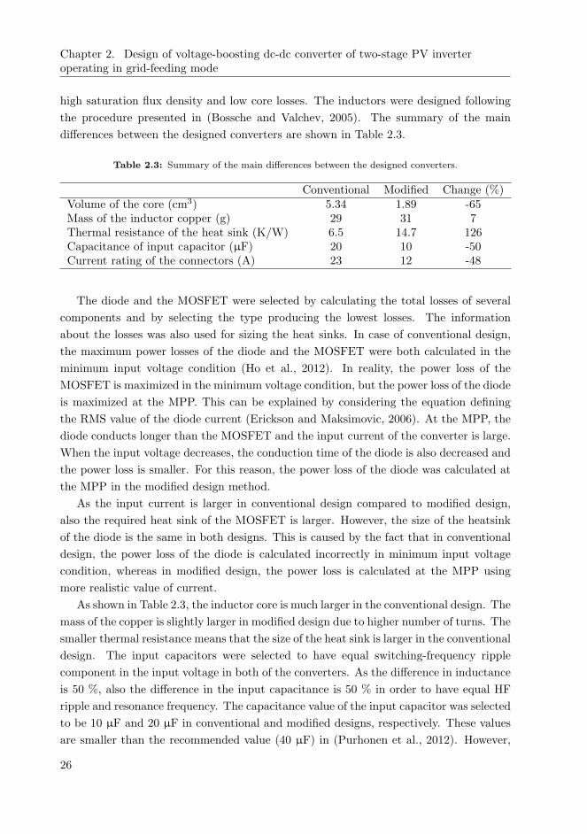
Chapter 2. Design of voltage-boosting dc-dc converter of two-stage PV inverteroperating in grid-feeding mode
high saturation flux density and low core losses. The inductors were designed following
the procedure presented in (Bossche and Valchev, 2005). The summary of the main
differences between the designed converters are shown in Table 2.3.
Table 2.3: Summary of the main differences between the designed converters.
Conventional Modified Change (%)Volume of the core (cm3) 5.34 1.89 -65Mass of the inductor copper (g) 29 31 7Thermal resistance of the heat sink (K/W) 6.5 14.7 126Capacitance of input capacitor (µF) 20 10 -50Current rating of the connectors (A) 23 12 -48
The diode and the MOSFET were selected by calculating the total losses of several
components and by selecting the type producing the lowest losses. The information
about the losses was also used for sizing the heat sinks. In case of conventional design,
the maximum power losses of the diode and the MOSFET were both calculated in the
minimum input voltage condition (Ho et al., 2012). In reality, the power loss of the
MOSFET is maximized in the minimum voltage condition, but the power loss of the diode
is maximized at the MPP. This can be explained by considering the equation defining
the RMS value of the diode current (Erickson and Maksimovic, 2006). At the MPP, the
diode conducts longer than the MOSFET and the input current of the converter is large.
When the input voltage decreases, the conduction time of the diode is also decreased and
the power loss is smaller. For this reason, the power loss of the diode was calculated at
the MPP in the modified design method.
As the input current is larger in conventional design compared to modified design,
also the required heat sink of the MOSFET is larger. However, the size of the heatsink
of the diode is the same in both designs. This is caused by the fact that in conventional
design, the power loss of the diode is calculated incorrectly in minimum input voltage
condition, whereas in modified design, the power loss is calculated at the MPP using
more realistic value of current.
As shown in Table 2.3, the inductor core is much larger in the conventional design. The
mass of the copper is slightly larger in modified design due to higher number of turns. The
smaller thermal resistance means that the size of the heat sink is larger in the conventional
design. The input capacitors were selected to have equal switching-frequency ripple
component in the input voltage in both of the converters. As the difference in inductance
is 50 %, also the difference in the input capacitance is 50 % in order to have equal HF
ripple and resonance frequency. The capacitance value of the input capacitor was selected
to be 10 µF and 20 µF in conventional and modified designs, respectively. These values
are smaller than the recommended value (40 µF) in (Purhonen et al., 2012). However,
26

2.3. Hardware design of voltage-boosting dc-dc converter
the measured switching-frequency ripple in the input voltage was 250 mV meaning that
its effect on the MPPT efficiency is negligible.
The presented small-signal model of voltage-boosting converter was used for the con-
trol design and for selecting the input capacitor. The frequency response of the control-
to-input-voltage transfer function including the effect of PV panel is shown in Fig. 2.4,
when the parameters of the modified design are used. As it is shown, the peaking is
stronger in CC region and the highest peaking occurs, when the input voltage is in
minimum value.
101
102
103
104
−100
20
40
60
Mag
nit
ude
(dB
)
101
102
103
104
0
45
90
135
180
Phas
e (d
eg)
Frequency (Hz)
cccv
Fig. 2.4: Control-to-input-voltage transfer function including the effect of PV panel outputimpedance.
High resonant peaking is a consequence of small parasitic resistances in the circuit.
On the other hand, the peaking is small in the CV region, because the small dynamic
resistance of the PV panel attenuates the resonant peaking. A damping circuit consisting
of series-connected resistor and capacitor was added in parallel with the input capacitor
to enable stable operation also in CC region. According to Fig. 2.4, gain margin should
be determined at the minimum input voltage and phase margin at the maximum input
voltage to guarantee that the converter is stable at every operating point.
As it was previously discussed, the dc-link voltage of the two-stage single-phase in-
verter contains ripple component at double-line frequency. This ripple can be prevented
from affecting the voltage of the PVG either by using dc-link voltage feedforward or
input-voltage control in the voltage-boosting converter. The reverse voltage transfer ra-
tio Toi describes the relation between the dc-link voltage and the voltage of the PVG. In
case of input-voltage-controlled converter, the reverse voltage transfer ratio is calculated
as shown in (A.12). According to (A.12) the attenuation is high, when the loop gain is
27
Chapter 2. Design of voltage-boosting dc-dc converter of two-stage PV inverteroperating in grid-feeding mode
high at double-line frequency.
The requirement for the control bandwidth of the input-voltage controller is deter-
mined by the MPPT. Fast MPPT requires high control bandwidth. In case of the con-
verters designed in this chapter, it was assumed that the MPPT is slow and the control
bandwidth can be below the resonant frequency. The shape of the loop gain is affected by
the capacitance value of the input capacitor and by the controller. I-type controller was
used and its parameters were selected by loop-shaping technique as a trade-off between
high attenuation from output to input voltage, small capacitance of the input capacitor
and adequate phase and gain margins.
2.3.3 Experimental evidence
The prototypes of the converters are shown in Fig. 2.5. As it is shown, the physical size of
the conventional design is bigger than the modified design as expected. The size difference
is clearest between the inductors, heatsinks of the MOSFET and the connectors. The
circuit boards shown in Fig. 2.5 include only the power stage, driver and measurement
circuit. The controller was placed on a separate circuit board and it was implemented
by using digital signal processor TMS28335F from Texas Instruments.
InductorInductor
Diode
DiodeMOSFET
MOSFET
a) b)
Fig. 2.5: The prototypes of a) conventional and b) modified designs.
The parameter values of the converters are presented in Table 2.4, where the symbols
refer to Fig. 2.2. As shown, the capacitance of the input capacitor and the inductance
of the inductor are dependent on the operating point, whereas other parameters are
constant. The capacitance value of the input capacitor is dependent on input voltage,
because ceramic capacitor was used. The inductance of the inductors dropped steeper
as a function of bias current than it was expected based on datasheet. In order to have
enough inductance at maximum current, two similarly designed inductors were connected
in series. As the input current is much lower than the maximum current at the operating
28

2.3. Hardware design of voltage-boosting dc-dc converter
points where the measurements were made, the inductance values in Table 2.4 are higher
than the required values 43 µH and 89 µH. The dependency of the inductance on the
bias current can be reduced by using discrete air gap.
Table 2.4: Parameter values of the prototype converters.
Parameter L1 rL1 C1 rC1 C2 rC2 VD rD rsw(µH) (mΩ) (µF) (mΩ) (µF) (mΩ) (V) (mΩ) (mΩ)
Conventional (CC) 69 6.4 16 4 52 120 0.39 100 20Conventional (CC) 85 6.4 6.6 4 52 120 0.39 100 20Modified (CC) 110 19.7 8 4 52 120 0.39 100 20Modified (CC) 173 19.7 3.3 4 52 120 0.39 100 20
The measurements were made by using Agilent E4360A Solar Array Simulator (SAS)
as a source emulating single Naps NP190GKg PV panel. The accuracy of this emulator
for emulating the dynamic behavior of the selected PV panel has been shown to be
sufficient for these type of measurements in (Nousiainen et al., 2013). The load was series
connection of three 12 V batteries parallel to Programmable DC load Chroma 63103A
operating in current sink mode. The measurements were repeated in CC and CV regions
and at the MPP. The corresponding operating points were 5V/7.98A, 31V/2.6A, and
25.9V/7.33A.
Thermal images of the converters operating at the MPP are shown in Fig. 2.6. These
images were taken using NEC TH7800 Thermo Tracer. The temperature scales in the
images are different from each other. The red color in Fig. 2.6a corresponds to white
color in Fig. 2.6b.
(a) Conventional design. (b) Modified design.
Fig. 2.6: Thermal images of the power stages, when operating at the MPP in STC.
According to Fig. 2.6, the temperature of the diode is around 62 C in both of the
converters as expected, because the heat sinks are identical. However, as the heat sink of
29
Chapter 2. Design of voltage-boosting dc-dc converter of two-stage PV inverteroperating in grid-feeding mode
the MOSFET is much larger in the conventionally designed converter, it is running cooler
similarly as the inductor. The temperature distribution is non-uniform in conventionally
designed converter, because the diode is running much hotter than other components.
On the other hand, the modified design method yields a more uniform temperature
distribution having the same maximum value of the temperature as in the conventionally
designed converter.
The higher temperature of the inductor in the modified design indicates that the
power losses are higher compared to the conventional design. The total efficiency of
the converter was measured and reported in (Viinamaki et al., 2014). According to
the measurements, the efficiency is approximately 0.4 p.u. lower at the MPP in the
modified design compared to the conventional design. This is the main disadvantage of
the modified design method.
The measured input-voltage loop gain and the closed-loop reverse voltage transfer
functions are shown in Figs. 2.7 and 2.8, respectively. They were measured by using the
frequency response analyzer Model 3120 by Venable Instruments. According to Fig. 2.7,
the minimum gain margin is 11 dB and the minimum phase margin is 82 in both of the
converters. The resonance peak is sufficiently attenuated by the damping circuit.
According to Fig. 2.8, the attenuation at the double-line frequency is 13 to 25 dB
depending on the operating point. Higher attenuation can be obtained by using PID con-
troller having bandwidth over the resonance instead of low-bandwidth I controller. In this
case, also the damping circuit can be removed. However, the crossover frequency should
be approximately one decade higher than the resonant frequency to obtain adequate
phase and gain margins. In addition, if the crossover frequency is close to resonance,
the phase and gain margins are more dependent on the operating point, especially, when
the parameter values are highly dependent on the operating point (see Table 2.4). In
this case, it might be compulsory to increase the inductance value or capacitance value
of the input capacitor to decrease the resonant frequency to obtain good gain and phase
margins by using reasonably low crossover frequency.
As the phase and gain margins and attenuation at double-line frequency are equal
in both converters, it can be concluded that the the same dynamic performance can be
obtained using either of these design methods and still the modified design method yield
material savings according to Table 2.3.
30

2.3. Hardware design of voltage-boosting dc-dc converter
101
102
103
104
−80
−60
−40
−20
0
20
Mag
nit
ud
e (d
B)
101
102
103
104
−270
−180
−90
0
90
Ph
ase
(deg
)
Frequency (Hz)
predicted
cccv
MINGM =11dB
MINPM =82o
predicted
cccv
(a) Conventional design.
101
102
103
104
−80
−60
−40
−20
0
20
Mag
nit
ude
(dB
)
101
102
103
104
−270
−180
−90
0
90
Phas
e (d
eg)
Frequency (Hz)
predicted
cccv
MINGM =11dB
MINPM =82o
predicted
cccv
(b) Modified design.
Fig. 2.7: Measured and predicted loop gains of the converters.
31

Chapter 2. Design of voltage-boosting dc-dc converter of two-stage PV inverteroperating in grid-feeding mode
101
102
103
104
−60
−40
−20
0
Mag
nit
ude
(dB
)
101
102
103
104
−180
−90
0
90
Phas
e (d
eg)
Frequency (Hz)
predicted
cccv
13dB
predicted
cccv
(a) Conventional design.
101
102
103
104
−60
−40
−20
0
Mag
nit
ud
e (d
B)
101
102
103
104
−180
−90
0
90
Ph
ase
(deg
)
Frequency (Hz)
cccvpredicted
13dB
predicted
cccv
(b) Modified design.
Fig. 2.8: Measured and predicted closed-loop reverse voltage transfer ratios of the converters.
32
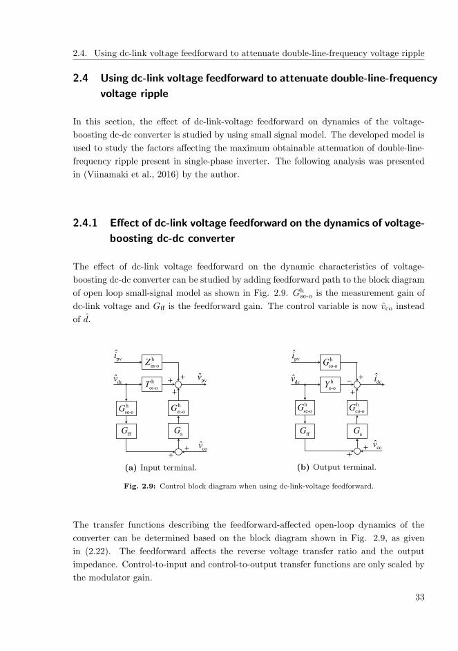
2.4. Using dc-link voltage feedforward to attenuate double-line-frequency voltage ripple
2.4 Using dc-link voltage feedforward to attenuate double-line-frequency
voltage ripple
In this section, the effect of dc-link-voltage feedforward on dynamics of the voltage-
boosting dc-dc converter is studied by using small signal model. The developed model is
used to study the factors affecting the maximum obtainable attenuation of double-line-
frequency ripple present in single-phase inverter. The following analysis was presented
in (Viinamaki et al., 2016) by the author.
2.4.1 Effect of dc-link voltage feedforward on the dynamics of voltage-
boosting dc-dc converter
The effect of dc-link voltage feedforward on the dynamic characteristics of voltage-
boosting dc-dc converter can be studied by adding feedforward path to the block diagram
of open loop small-signal model as shown in Fig. 2.9. Ghse-o is the measurement gain of
dc-link voltage and Gff is the feedforward gain. The control variable is now vco instead
of d.
h
ci-oGh
se-oG
h
in-oZ
h
oi-oT
pvi
dcv
cov
pvv
ffG aG
(a) Input terminal.
h
io-oG
h
o-oY
h
co-oG
pvi
dcv dci
cov
h
se-oG
aGffG
(b) Output terminal.
Fig. 2.9: Control block diagram when using dc-link-voltage feedforward.
The transfer functions describing the feedforward-affected open-loop dynamics of the
converter can be determined based on the block diagram shown in Fig. 2.9, as given
in (2.22). The feedforward affects the reverse voltage transfer ratio and the output
impedance. Control-to-input and control-to-output transfer functions are only scaled by
the modulator gain.
33
Chapter 2. Design of voltage-boosting dc-dc converter of two-stage PV inverteroperating in grid-feeding mode
[
vpv
idc
]
=
[
Zh-ffin-o T h-ff
oi-o Gh-ffci-o
Gh-ffio-o −Y h-ff
o-o Gh-ffco-o
]
ipv
vdc
vco
=
[
Zhin-o T h
oi-o +Ghci-oGaG
hse-oGff Gh
ci-oGa
Ghio-o Y h
o-o −Ghco-oGaG
hse-oGff Gh
co-oGa
]
ipv
vdc
vco
(2.22)
The target is to prevent the double-line-frequency voltage ripple from affecting the
PVG voltage. The attenuation from dc-link voltage to PVG voltage is maximized, when
the magnitude of reverse voltage transfer ratio is zero as
T hoi-o +Gh
ci-oGaGhse-oGff = 0. (2.23)
The required feedforward gain can now be solved by substituting (2.11) and (2.12) to
(2.23). When assuming unity modulator and measurement gains, the required feedfor-
ward gain is
Gff =Vpv
V 2dc
1− (rL+rsw)IpvVpv
1 +2VdcVD+2Vdc(rD−rsw)Ipv+V 2
D+2VD(rD−rsw)Ipv+((rD−rsw)Ipv)
2
V 2dc
. (2.24)
The feedforward gain is presented in (2.24) by separating the term Vpv/V2dc. This term is
called here an ideal feedforward gain, because it would yield infinite attenuation in case
of a lossless converter. The remaining part in (2.24) includes the parasitic elements. As
it would be difficult to include all these parasitic elements in practical implementation
of feedforward, ideal feedforward gain is used in practice. However, as the real converter
includes losses, the resulting reverse voltage transfer function is not zero, i.e., the attenu-
ation is not infinite. This loss-affected attenuation can be calculated by substituting the
ideal feedforward gain, (2.11), and (2.12) into (2.22) yielding
T h-ffoi-o = T h
oi-o +Ghci-oG
hff =
1 + srC1C1
∆LC1
(
D′ − VeqVpv
V 2dc
)
. (2.25)
The effect of feedforward on the reverse-voltage transfer function can be studied in a
frequency range from low frequencies up to half the switching frequency by using (2.25).
It is useful as the dc-link voltage might include also higher frequency components to
34
2.4. Using dc-link voltage feedforward to attenuate double-line-frequency voltage ripple
be attenuated. The effect of parameter variation on double-line-frequency attenuation
is studied in the next section. Thus, (2.25) is further simplified by approximating its
low-frequency value by setting s=0 resulting (2.26).
T h-ff-lfoi-o = D′ − Veq
Vpv
V 2dc
=V 2dc (Vpv − (rL + rsw) Ipv)− Vpv (Vdc + VD + (rD − rsw) Ipv)
2
V 2dc (Vdc + VD + (rD − rsw) Ipv)
(2.26)
The effect of dc-link voltage feedforward on the output impedance of the converter is
of interest as the output impedance affects the dc-link-voltage control loop in a two-stage
PV inverter (Messo et al., 2014). The low-frequency value of the feedforward-affected
output impedance can be calculated by first substituting the ideal feedforward gain,
(2.14) and (2.15) to (2.22), then setting s=0 yielding
Y h-ff-lfo-o =
IpvVpv
V 2dc
=IpvD
′
Vdc=
IdcVdc
=⇒ Zh-ff-lfo-o =
Vdc
Idc. (2.27)
As it was mentioned earlier, the output impedance of PV generator is operation-point
dependent and it affects the dynamics of the interfacing converter. The equations for
including the effect of source admittance on the h-parameter set are shown in Appendix
A. The source-affected output admittance can be calculated as
Y hSo =
1 + Ys
(
Zhin +
GhioT
hoi
Y ho
)
1 + YsZhin
Y ho , (2.28)
where Ys is the source admittance, which in this case is the output admittance of the
PVG. When the dc-link feedforward is used, the magnitude of the reverse voltage transfer
function is small, implicating that the factor multiplied with Y ho is close to unity and
Y hSo ≈ Y h
o . Thus, according to (2.27), the source-affected output impedance depends
only on the dc-link voltage and current, i.e., the converter has constant power output
similarly as in case of input-voltage-controlled converter (Messo et al., 2012). This prop-
erty of the converter effectively removes the right-half-plane (RHP) pole existing in the
control dynamics of the dc-link-voltage control of the inverter caused by the PVG. As
the RHP pole is removed, there is no lower limit for the crossover frequency of the dc-
link voltage loop of the inverter. If no feedforward or input-voltage control is used, the
stable operating range of the inverter is limited, because the crossover frequency of the
dc-link-voltage control loop must be higher than the frequency of the RHP pole.
35

Chapter 2. Design of voltage-boosting dc-dc converter of two-stage PV inverteroperating in grid-feeding mode
In case of voltage-boosting converter, the conventional method to implement dc-link
voltage feedforward is based on the equation of steady-state duty cycle D. Instead of
using constant values, when calculating the duty cycle, the measured value of the dc-link
voltage is used. By neglecting the losses, the average value of the duty cycle is
d = 1− 〈vc〉〈vdc〉
, (2.29)
where vc is the desired value of the PVG voltage and vdc is the measured dc-link voltage.
Linearization of (2.29) yield
d = − 1
Vdcvc +
Vc
V 2dc
vdc = qovc +Gffvdc. (2.30)
By comparing (2.30) to (2.24) and the block digram in Fig. 2.9, it can be noted that
the conventional method produces ideal feedforward gain and its dynamic effect is as in
Fig. 2.9, when assuming unity modulator gain and when vco = qovc. Thus, the presented
analysis is valid, when using conventional implementation of voltage feedforward.
2.4.2 Effect of parameter variation on low-frequency ripple attenua-
tion
The effect of parameter variation on the performance of dc-link-voltage feedforward was
studied numerically using the parameter values of the converter designed in the previous
chapter. The low-frequency magnitude of reverse-voltage transfer function is shown in
Fig. 2.10 as a function of measurement gain Gse-o.
0 0.5 1 1.5 2−60
−50
−40
−30
−20
−10
0
Gse−o
Toi−
o
ovff
−lf (
dB
)
Fig. 2.10: The effect of measurement gain on the magnitude of reverse voltage transfer ratio,when Vpv = 25.9 V and Vdc = 38 V.
36
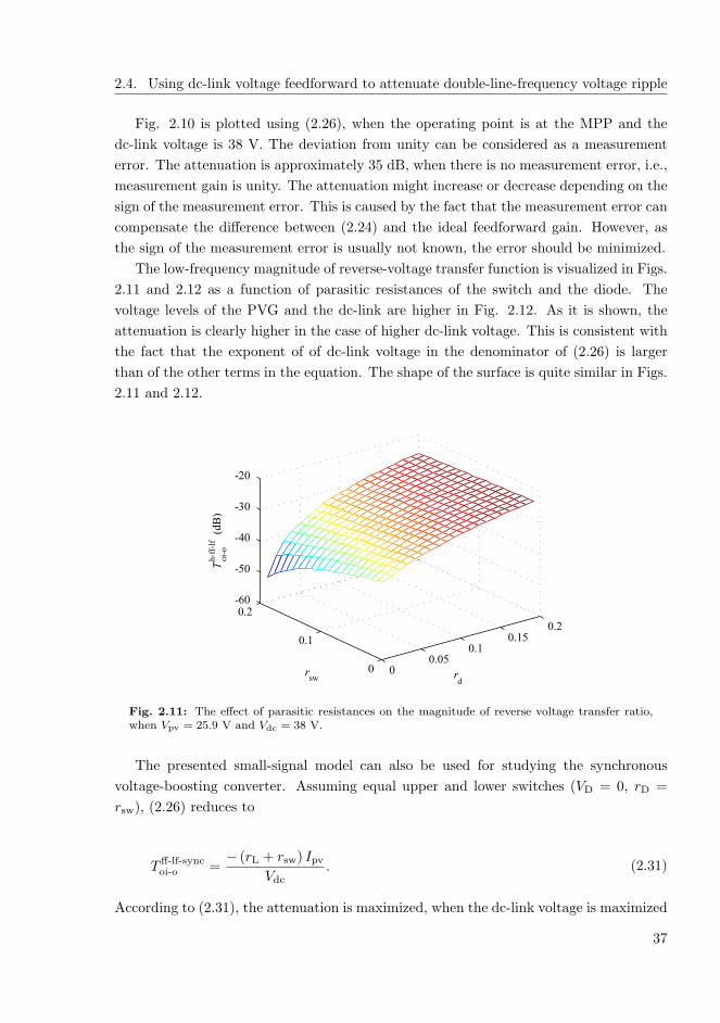
2.4. Using dc-link voltage feedforward to attenuate double-line-frequency voltage ripple
Fig. 2.10 is plotted using (2.26), when the operating point is at the MPP and the
dc-link voltage is 38 V. The deviation from unity can be considered as a measurement
error. The attenuation is approximately 35 dB, when there is no measurement error, i.e.,
measurement gain is unity. The attenuation might increase or decrease depending on the
sign of the measurement error. This is caused by the fact that the measurement error can
compensate the difference between (2.24) and the ideal feedforward gain. However, as
the sign of the measurement error is usually not known, the error should be minimized.
The low-frequency magnitude of reverse-voltage transfer function is visualized in Figs.
2.11 and 2.12 as a function of parasitic resistances of the switch and the diode. The
voltage levels of the PVG and the dc-link are higher in Fig. 2.12. As it is shown, the
attenuation is clearly higher in the case of higher dc-link voltage. This is consistent with
the fact that the exponent of of dc-link voltage in the denominator of (2.26) is larger
than of the other terms in the equation. The shape of the surface is quite similar in Figs.
2.11 and 2.12.
00.05
0.10.15
0.2
0
0.1
0.2-60
-50
-40
-30
-20
rd
rsw
Toi-
o
h-f
f-lf
(dB
)
Fig. 2.11: The effect of parasitic resistances on the magnitude of reverse voltage transfer ratio,when Vpv = 25.9 V and Vdc = 38 V.
The presented small-signal model can also be used for studying the synchronous
voltage-boosting converter. Assuming equal upper and lower switches (VD = 0, rD =
rsw), (2.26) reduces to
Tff-lf-syncoi-o =
− (rL + rsw) IpvVdc
. (2.31)
According to (2.31), the attenuation is maximized, when the dc-link voltage is maximized
37

Chapter 2. Design of voltage-boosting dc-dc converter of two-stage PV inverteroperating in grid-feeding mode
and the parasitic resistances of the switches and inductor are minimized. The illustration
is shown in Fig. 2.13, where (2.31) is used to plot the low-frequency magnitude of reverse
voltage transfer function in case of synchronous converter and dc-link voltage of 700 V.
As a conclusion, the highest attenuation for double-line frequency is obtained by using as
high dc-link voltage as possible, by minimizing the parasitic resistances of the switches
and inductor as well as using a synchronous converter instead of diode-switched converter.
00.05
0.10.15
0.2
0
0.1
0.2-70
-65
-60
-55
-50
rd
rsw
Toi-
o
h-f
f-lf
(dB
)
Fig. 2.12: The effect of parasitic resistances on the magnitude of reverse voltage transfer ratio,when Vpv = 400 V and Vdc = 700 V.
00.05
0.10.15
0.2
0
0.1
0.2-75
-70
-65
-60
-55
-50
-45
rL
rsw
Toi-
o
h-f
f-lf
(dB
)
Fig. 2.13: The effect of parasitic resistances on the magnitude of reverse voltage transfer ratio,when Vpv = 400 V and Vdc = 700 V in case of synchronous converter.
38
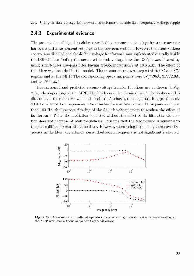
2.4. Using dc-link voltage feedforward to attenuate double-line-frequency voltage ripple
2.4.3 Experimental evidence
The presented small-signal model was verified by measurements using the same converter
hardware and measurement setup as in the previous section. However, the input voltage
control was disabled and the dc-link-voltage feedforward was implemented digitally inside
the DSP. Before feeding the measured dc-link voltage into the DSP, it was filtered by
using a first-order low-pass filter having crossover frequency at 10.6 kHz. The effect of
this filter was included in the model. The measurements were repeated in CC and CV
regions and at the MPP. The corresponding operating points were 5V/7.98A, 31V/2.6A,
and 25.9V/7.33A.
The measured and predicted reverse voltage transfer functions are as shown in Fig.
2.14, when operating at the MPP. The black curve is measured, when the feedforward is
disabled and the red curve, when it is enabled. As shown, the magnitude is approximately
30 dB smaller at low frequencies, when the feedforward is enabled. At frequencies higher
than 100 Hz, the low-pass filtering of the dc-link voltage starts to weaken the effect of
feedforward. When the prediction is plotted without the effect of the filter, the attenua-
tion does not decrease at high frequencies. It seems that the feedforward is sensitive to
the phase difference caused by the filter. However, when using high enough crossover fre-
quency in the filter, the attenuation at double-line frequency is not significantly affected.
101
102
103
104
-60
-40
-20
0
20
Mag
nit
ude
(dB
)
101
102
103
104
-180
-90
0
90
180
Phas
e (d
eg)
Frequency (Hz)
predictedwith FFwithout FF
Fig. 2.14: Measured and predicted open-loop reverse voltage transfer ratio, when operating atthe MPP with and without output-voltage feedforward.
39
Chapter 2. Design of voltage-boosting dc-dc converter of two-stage PV inverteroperating in grid-feeding mode
The reverse voltage transfer function was measured also in CC and CV regions, when
the feedforward was enabled and the result is shown in Fig. 2.15. As it is shown, the
magnitude at double-line frequency is approximately -35 dB at all the measured operating
points. There is also a good match between the measured and predicted curves. The
difference in the phase curves at the high frequencies is caused by the control delay of
the DSP, which was not modeled.
101
102
103
104
-60
-40
-20
0
20
Mag
nit
ude
(dB
)
101
102
103
104
-180
-90
0
90
180
Phas
e (d
eg)
Frequency (Hz)
predictedcvcc
Fig. 2.15: Measured and predicted open-loop reverse voltage transfer ratio, when operating in CCand CV regions and using output-voltage feedforward.
The measured and predicted output impedances of the prototype converter are shown
in Fig. 2.16. Black, blue and red lines indicate the operation in CC and CV regions
and at the MPP, respectively. According to Fig. 2.16a, the output impedance of the
converter is affected by the operating-point-dependent impedance of the PV generator,
when operating in open loop. When the dc-link-voltage feedforward is enabled, the
output impedance becomes a function of ouput power of the converter as shown in Fig.
2.16b. The output power is approximately 40 W, 80 W, and 190 W at the measured
operating points in the CC and CV regions and at the MPP, respectively. Calculating
the low-frequency output impedance values using (2.27) yields 36 Ω, 18 Ω and 7.6 Ω for
CC, CV and MPP, respectively. These values match well with Fig. 2.16b verifying the
analysis.
40
2.4. Using dc-link voltage feedforward to attenuate double-line-frequency voltage ripple
101
102
103
104
-20
0
20
40
Mag
nit
ude
(dB
)
101
102
103
104
-90
-45
0
45
90
Phas
e (d
eg)
Frequency (Hz)
predicted
cc
cvmpp
(a) Feedforward is not in use.
101
102
103
104
-20
0
20
40
Mag
nit
ude
(dB
)
101
102
103
104
-90
-45
0
45
90
Phas
e (d
eg)
Frequency (Hz)
predicted
cc
cvmpp
(b) Feedforward is in use.
Fig. 2.16: Measured and predicted output impedance of the converter.
Finally, the effect of voltage feedforward on the attenuation of double-line frequency
voltage ripple was demonstrated by time-domain measurements. Sinusoidal voltage was
summed to the dc-link voltage by connecting a linear amplifier in series with the load.
The reference signal for the amplifier was generated by a signal generator. By comparing
Figs. 2.17a and 2.17b, it can be seen that the addition of dc-link-voltage feedforward
effectively prevents the double-line-frequency ripple of the dc-link voltage to affect the
PVG voltage.
41
Chapter 2. Design of voltage-boosting dc-dc converter of two-stage PV inverteroperating in grid-feeding mode
Time (2 ms / div)
pv (2 V / div)v
dc (2 V / div)v
(a) Feedforward is not in use.
Time (2 ms / div)
pv (2 V / div)v
dc (2 V / div)v
(b) Feedforward is in use.
Fig. 2.17: Measured low-frequency voltage ripple in dc-link and PV voltage.
2.5 Conclusions
The properties of the PVG were studied to find analytical equations for the maximum OC
voltage, minimumMPP voltage and the maximum SC current. These equations, together
with the measurement data on solar irradiance and ambient temperature, were used to
calculate the required input voltage and current ranges of the interfacing converter. It
was shown that the maximum SC current available from the PVG is approximately 1.4
times the SC current in STC. If the partial shading is taken into account, the minimum
MPP voltage occurs, when only one PV cell group is producing current to the output and
other groups are shaded. The maximum OC voltage was found to occur in April, when
the ambient temperature was 1.9 C and the solar irradiance was 1400 W/m2. These
values give good approximation, when the PVG is located in Finland or in other Nordic
countries.
The design of the voltage-boosting dc-dc converter of two-stage PV inverter was stud-
ied. The PV inverter was assumed to operate in grid-feeding mode meaning that the dc-
link voltage is controlled by the dc-ac inverter and the voltage of the PVG is controlled
by the dc-dc converter. The dc-ac inverter was left out from the analysis as the focus
was on the dc-dc converter.
Two interfacing converters were designed for Naps NP190GKg PV panel to study
42

2.5. Conclusions
the component sizing. In the conventionally designed converter, the maximum input
current of the converter was calculated by dividing the nominal power of the converter
by the minimum input voltage. In the other converter (modified design), the maximum
input current was determined by using the real maximum current of the PV panel. In
addition, the power losses of the diode were calculated in the minimum-input-voltage
condition in case of conventional design, and at the MPP in case of the modified design.
According to the investigations, using modified design instead of conventional design in
case of wide input-voltage range yields smaller inductor core, smaller heat sink of the
MOSFET, smaller input capacitor and more even temperature distribution.
A small-signal model of voltage-boosting converter having dc-link-voltage feedforward
was developed. The developed model was used to study the effect of feedforward on the
attenuation of double-line-frequency voltage ripple from the dc-link to the PVG. It was
shown, that the highest attenuation is obtained by using as high dc-link voltage as possi-
ble, minimized parasitic resistances of the switches and inductor and using synchronous
converter instead of diode-switched converter. In addition, when using dc-link-voltage
feedforward, the output impedance of the converter depends only on the dc-link voltage
and current, i.e., the converter has constant power output similarly as in case of input-
voltage-controlled converter. When considering the two-stage PV inverter, this property
of the converter removes the right-half-plane (RHP) pole existing in the control loop
of the dc-ac inverter. As the control bandwidth of the inverter must be higher than
the frequency of this RHP pole, there is no such restriction, when using dc-link-voltage
feedforward.
43

3 DESIGN OF VOLTAGE-BOOSTING DC-DC
CONVERTER OF TWO-STAGE PV INVERTER
OPERATING IN GRID-FORMING MODE
In this chapter, a small-signal model of voltage-boosting dc-dc converter operating as a
part of two-stage PV inverter is developed, when the inverter is operating in grid-forming
mode. This means that the dc-link voltage is controlled by the dc-dc converter. The
properties of the PVG are taken into account but the dc-ac inverter is neglected similarly
as in the previous chapter. The model is used for studying the dynamic properties of the
converter affecting the control design and component selection. The material presented
in this chapter is based on (Viinamaki et al., 2017).
3.1 Small-signal modeling of the converter
In Chapter 2, the small-signal model of the voltage-boosting converter was developed
for grid-feeding operation. In this case, the PVG was modeled as a current source,
because the voltage of the PVG was controlled. Furthermore, as the dc-link voltage was
controlled by the inverter, the load was modeled as constant voltage sink. Contrary
to this, in grid-forming operation, the load of the converter is modeled as a constant
current sink, because the dc-link voltage is controlled by the converter. Another major
difference is that the voltage or current of the PVG is not controlled by the converter.
This suggests that the PVG can be modeled either as a current source or a voltage source
for determining the control-to-output transfer function used in the control design. For
this reason, the small-signal model of the converter is developed by using current source
(z-parameter model) and voltage source (g-parameter model) and their differences are
studied.
The topology of the studied converter is the same as in Chapter 2. Only the source and
load are different due to different control schemes as shown in Fig. 3.1. The developed
small-signal models are used for studying the dynamics of the converter in grid-forming
operation. Special attention is paid to the existence of RHP zeros as they have major
effect on the control design. According to control engineering principles, the bandwidth
of the control loop must be limited to lower than the frequency of the RHP zero or zeros
to obtain stable control loop.
45
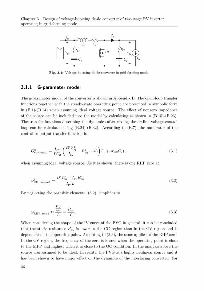
Chapter 3. Design of voltage-boosting dc-dc converter of two-stage PV inverteroperating in grid-forming mode
pvi
1C
L
sw
2C
dcv
dci
pvv
Lr
C2rC1r
DV
Fig. 3.1: Voltage-boosting dc-dc converter in grid-forming mode.
3.1.1 G-parameter model
The g-parameter model of the converter is shown in Appendix B. The open-loop transfer
functions together with the steady-state operating point are presented in symbolic form
in (B.1)-(B.14) when assuming ideal voltage source. The effect of nonzero impedance
of the source can be included into the model by calculating as shown in (B.15)-(B.23).
The transfer functions describing the dynamics after closing the dc-link-voltage control
loop can be calculated using (B.24)-(B.32). According to (B.7), the numerator of the
control-to-output transfer function is
Ggco-o-num =
IpvLC2
(
D′V geq
Ipv−Rg
eq − sL
)
(1 + srC2C2) , (3.1)
when assuming ideal voltage source. As it is shown, there is one RHP zero at
ωgRHP−zero1 =
D′V geq − IpvR
geq
IpvL. (3.2)
By neglecting the parasitic elements, (3.2), simplifies to
ωgRHP-zero1 ≈
Vpv
Ipv
L=
Rpv
L. (3.3)
When considering the shape of the IV curve of the PVG in general, it can be concluded
that the static resistance Rpv is lower in the CC region than in the CV region and is
dependent on the operating point. According to (3.3), the same applies to the RHP zero.
In the CV region, the frequency of the zero is lowest when the operating point is close
to the MPP and highest when it is close to the OC condition. In the analysis above the
source was assumed to be ideal. In reality, the PVG is a highly nonlinear source and it
has been shown to have major effect on the dynamics of the interfacing converter. For
46

3.1. Small-signal modeling of the converter
this reason, also the source-affected control-to-output transfer function was determined
symbolically. The impedance of the PVG is approximated using the dynamic resistance
rpv in the following equations for simplicity. For a more exact model, the measured
output impedance of the PVG can be included directly in the model. However, the
dynamic resistance offers adequate approximation for the following analysis.
The ideal (infinite bandwidth) input admittance Yin-∞ was first calculated by substi-
tuting (B.2),(B.5),(B.4), and (B.7) into (B.23) resulting
Y gin-∞ = Y g
in −Gg
ioGgci
Ggco
=LC1
(
s2 − s(
D′V
geq
LIpv− R
geq+rC1
L
)
+ 1LC1
)
(
sL− D′Vgeq
Ipv+Rg
eq
)
(1 + srC1C1). (3.4)
Next, (3.4) was substituted together with (B.2) and (B.7) into (B.21). The resulting
source-affected control-to-output transfer function can be presented by dividing it into
the following equations
Ggco-oS = −Ipv
C2
(
s2 − sA1 −A0)
(1 + srC2C2)
s3 + s2B2 + sB1 +B0(3.5)
A1 =D′V g
eq
IpvL−
rC1rpv +Rgeq (rC1 + rpv)
L (rC1 + rpv)− 1
C1 (rC1 + rpv)(3.6)
A0 =D′V g
eq − Ipv(
Rgeq + rpv
)
IpvLC1 (rC1 + rpv)(3.7)
B2 =C1
(
Rgeq (rC1 + rpv) + rC1rpv
)
+ L
LC1 (rC1 + rpv)(3.8)
B1 =C2
(
Rgeq + rpv
)
+ C1D′2 (rC1 + rpv)
LC1C2 (rC1 + rpv)(3.9)
B0 =D′2
LC1C2 (rC1 + rpv). (3.10)
By neglecting the parasitic elements, Ggco-oS simplifies to
Ggco-oS ≈ −Ipv
C2
s2 − s(
Rpv
L− 1
rpvC1
)
+1−
Rpvrpv
LC1
s3 + s21
rpvC1+ sC2+D′2C1
LC1C2+ D′2
LC1C2rpv
. (3.11)
47
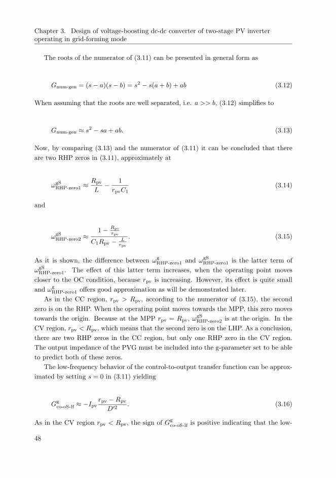
Chapter 3. Design of voltage-boosting dc-dc converter of two-stage PV inverteroperating in grid-forming mode
The roots of the numerator of (3.11) can be presented in general form as
Gnum-gen = (s− a)(s− b) = s2 − s(a+ b) + ab (3.12)
When assuming that the roots are well separated, i.e. a >> b, (3.12) simplifies to
Gnum-gen ≈ s2 − sa+ ab. (3.13)
Now, by comparing (3.13) and the numerator of (3.11) it can be concluded that there
are two RHP zeros in (3.11), approximately at
ωgSRHP-zero1 ≈ Rpv
L− 1
rpvC1(3.14)
and
ωgSRHP-zero2 ≈
1− Rpv
rpv
C1Rpv − L
rpv
. (3.15)
As it is shown, the difference between ωgRHP-zero1 and ωgS
RHP-zero1 is the latter term of
ωgSRHP-zero1. The effect of this latter term increases, when the operating point moves
closer to the OC condition, because rpv is increasing. However, its effect is quite small
and ωgRHP-zero1 offers good approximation as will be demonstrated later.
As in the CC region, rpv > Rpv, according to the numerator of (3.15), the second
zero is on the RHP. When the operating point moves towards the MPP, this zero moves
towards the origin. Because at the MPP rpv = Rpv, ωgSRHP-zero2 is at the origin. In the
CV region, rpv < Rpv, which means that the second zero is on the LHP. As a conclusion,
there are two RHP zeros in the CC region, but only one RHP zero in the CV region.
The output impedance of the PVG must be included into the g-parameter set to be able
to predict both of these zeros.
The low-frequency behavior of the control-to-output transfer function can be approx-
imated by setting s = 0 in (3.11) yielding
Ggco-oS-lf ≈ −Ipv
rpv −Rpv
D′2. (3.16)
As in the CV region rpv < Rpv, the sign of Ggco-oS-lf is positive indicating that the low-
48

3.1. Small-signal modeling of the converter
frequency phase starts at zero. As an opposite, in CC region the sign of Ggco-oS-lf is
negative indicating that the low-frequency phase will change by 180. Thus, the same
controller cannot be used in both of these operating regions. If the aim is to design a
controller, which is stable in the CC region, the dc gain of the controller must be negative.
If the controller is designed to be stable in the CV region, the dc gain of the controller
must be positive.
3.1.2 Z-parameter model
The z-parameter model of voltage-boosting dc-dc converter is presented in Appendix C
similarly as the g-parameter model in Appendix B. According to (B.7), the numerator
of the control-to-output transfer function is
Gzco-o-num = −Ipv
C2
(
s2 − sD′V z
eq −RzeqIpv
IpvL+
1
LC1
)
(1 + srC2C2) . (3.17)
By making similar assumption of well separated roots and using (3.13) as in the previous
section, it can be concluded that Gzco-o includes two RHP zeros at
ωzRHP-zero1 ≈
D′V zeq −Rz
eqIpv
IpvL(3.18)
and
ωzRHP-zero2 ≈ Ipv
C1
(
D′V zeq −Rz
eqIpv) . (3.19)
By neglecting the parasitic elements, (3.18) and (3.19) are simplifed to
ωzRHP-zero1 ≈ Rpv
L(3.20)
and
ωzRHP-zero2 ≈ 1
RpvC1. (3.21)
By neglecting the parasitic elements, ωzRHP-zero1 is exactly the same as ωg
RHP-zero1,
which was predicted by the g-parameter model. The second RHP zero existing only in
49

Chapter 3. Design of voltage-boosting dc-dc converter of two-stage PV inverteroperating in grid-forming mode
the CC region was not predicted by the g-parameter model without the effect of the
source impedance. However, the z-parameter model is able to produce approximation
also of this second RHP zero even if the source impedance is not taken into account.
The ideal input impedance Zin-∞ can be calculated by substituting (C.2),(C.5),(C.4),
and (C.7) into (C.26) resulting
Zzin-∞ = Zg
in − GzioG
zci
Gzco
=
(
sL− D′V
zeq
Ipv+Rz
eq − rC1
)
(1 + srC1C1)
LC1
(
s2 − s(
D′V zeq
LIpv− Rz
eq
L
)
+ 1LC1
) . (3.22)
The source-affected control-to-output transfer function can now be calculated by sub-
stituting (3.22) together with (C.2) and (C.7) into (C.24) resulting following group of
equations
Gzco-oS = −Ipv
C2
(
s2 − sA1 −A0)
(1 + srC2C2)
s3 + s2B2 + sB1 +B0(3.23)
A1 =D′V z
eq
IpvL−
Rzeq (rC1 + rpv)− r2C1
L (rC1 + rpv)− 1
C1 (rC1 + rpv)(3.24)
A0 =D′V z
eq − Ipv(
Rzeq + rpv − rC1
)
IpvLC1 (rC1 + rpv)(3.25)
B2 =C1
(
Rzeq (rC1 + rpv)− r2C1
)
+ L
LC1 (rC1 + rpv)(3.26)
B1 =C2
(
Rzeq + rpv − rC1
)
+ C1D′2 (rC1 + rpv)
LC1C2 (rC1 + rpv)(3.27)
B0 =D′2
LC1C2 (rC1 + rpv). (3.28)
Similarly as Ggco-oS, also Gz
co-oS can be simplified by neglecting the parasitic elements as
Gzco-oS ≈ −Ipv
C2
s2 − s(
Rpv
L− 1
rpvC1
)
+1−
Rpvrpv
LC1
s3 + s21
rpvC1+ sC2+D′2C1
LC1C2+ D′2
LC1C2rpv
. (3.29)
By comparing (3.5)-(3.10) and (3.23)-(3.28) it can be noted, that there are small
differences. These differences can be explained by the fact that rC1 is included in Rzeq
but not in Rgeq. If this detail is taken into account, it can be noted that g- and z-parameter
models produce exactly the same source-affected control-to-output transfer function. As
also approximated transfer functions (3.11) and (3.29) are equal, the zeros in (3.14) and
50
3.1. Small-signal modeling of the converter
(3.15) can be predicted either by g- or z-parameter models.
3.1.3 Small-signal stability of the interface between the PVG and the
converter
The closed-loop transfer functions of g- and h-parameter models are shown in Appendix
B and C, when the dc-link-voltage control loop is closed. According to (B.25) and (C.28),
the closed-loop input admittance and impedance can be calculated as
Y gin-c =
Y gin-o
1 + Lgout
+Lgout
1 + Lgout
Y gin-∞ (3.30)
Zzin-c =
Zzin-o
1 + Lzout
+Lzout
1 + Lzout
Zzin-∞. (3.31)
At the frequencies below the crossover frequency of the controller, it can be assumed
that the loop gain Lout >> 1. In this case, according to (3.31), the closed-loop input
impedance of the converter can be approximated by the ideal input impedance Zzin-∞ or
by the inverse of the ideal input admittance Y gin-∞. The low-frequency value of the ideal
input impedance can be approximated by setting s = 0 in (3.22) yielding
Zzin-c-lf = −
DV zeq
Ipv+Rz
eq − rC2. (3.32)
By neglecting parasitic elements, (3.32) simplifies to
Zzin-c-lf ≈ −Rpv. (3.33)
When the controller is designed to have stable operation in the CV region, the conven-
tional minor loop gain (Zpv/Zin-c) must be used in the stability analysis (Middlebrook,
1978). When using the low-frequency approximation without parasitic elements, the mi-
nor loop gain is −rpv/Rpv. As in the CV region rpv < Rpv, the absolute value of the
minor loop gain is always less than unity. According to the Nyquist stability criterion,
the system is stable in this case. At the MPP, rpv = Rpv yielding a minor loop gain of -1,
which means that the system is unstable. In addition, the system is unstable in the CC
region, where rpv > Rpv. In the CV region the duty cycle must be increased to increase
the dc-link voltage. When the operating point moves into the CC region, the duty ratio
should be decreased to increase the dc-link voltage. As the controller is designed for
stable operation in the CV region, the voltage will collapse and the control system will
51
Chapter 3. Design of voltage-boosting dc-dc converter of two-stage PV inverteroperating in grid-forming mode
not recover even if the overload condition is removed.
According to (Suntio and Leppaaho, 2010), the inverse minor loop gain (Zin-c/Zpv)
shall be used in the impedance-based-stability analysis of CF converters. When using
inverse minor loop gain, the system is stable only in the CC region as rpv > Rpv and
becomes unstable when the operating point is moved into MPP or CV region. This would
require that the controller gain is negative as it was explained in the previous chapter. In
case of instability, the voltage will collapse forcing the converter back into the CC region.
If the instability is caused by the permanent overload, the converter will stay unstable.
However, if the overload is caused by the transitory overload, the controller will continue
its normal operation right after the overload condition is removed.
Based on the previous discussion, the impedance ratio to be used in impedance-based-
stability analysis is different, when the converter is designed for stable operation in the
CV region or the CC region. For stable operation in the CC region the correct impedance
ratio is obtained by using the z-parameter model (VF-CO), and for stable operation in
the CV region the correct ratio is obtained by using the g-parameter model (CF-CO).
Thus, it is recommended to use z-parameter model for the converter designed for CC
operation and g-parameter model for the converter designed for CV operation, in order
to avoid mistakes in impedance-based-stability analysis.
3.2 DC-link-voltage control design
The presented theoretical findings were verified by designing a prototype converter em-
ploying dc-link voltage control. The converter hardware was the same as in Chapter 2.
However, the inductor, input capacitor and output capacitor were changed and different
PV panel was used. The reason for changing the PV panel was that that we wanted to
use a real PV panel instead of the PV emulator. The only artificial light unit that was
available was for the PV panel having lower power level. By using the real PV panel, it
was ensured that the dynamics of the laboratory setup was as close as possible to the
real system.
The PV panel used in this study was SR30-36 manufactured by Raloss. It consist
of 36 series connected PV cells, and the rated MPP power is 30 W at the STC. The
artificial light unit used for lighting the PV panel was able to produce 500 W/m2 solar
irradiance, yielding approximately 15W power at the MPP. As the same PV panel and
artificial light unit were used in the prior research by Leppaaho et al. the existing data
of output impedance and IV curve of the panel was used for plotting Figs. 3.2-3.5.
The measured IV curve is shown in Fig. 3.2. The dynamic resistance of the PV
panel was extracted from the measured output impedance in several operating points.
The extracted dynamic resistance and static resistance are shown in Fig. 3.2 below the
IV curve. The dots represent measured/calculated values and the solid line is the trend
52
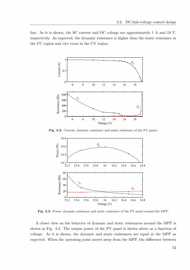
3.2. DC-link-voltage control design
line. As it is shown, the SC current and OC voltage are approximately 1 A and 19 V,
respectively. As expected, the dynamic resistance is higher than the static resistance in
the CC region and vice versa in the CV region.
6 8 10 12 14 16 180
0.5
1C
urr
ent
(A)
6 8 10 12 14 16 180
200
400
600
800
Res
ista
nce
(Ω
))
Voltage (V)
pvP
pvr
pvR
Fig. 3.2: Current, dynamic resistance and static resistance of the PV panel.
15.2 15.4 15.6 15.8 16 16.2 16.4 16.6 16.814.2
14.4
14.6
14.8
Pow
er (
W)
15.2 15.4 15.6 15.8 16 16.2 16.4 16.6 16.80
20
40
60
80
Res
ista
nce
(Ω
))
Voltage (V)
pvr
pvR
pvP
Fig. 3.3: Power, dynamic resistance and static resistance of the PV panel around the MPP.
A closer view on the behavior of dynamic and static resistances around the MPP is
shown in Fig. 3.3. The output power of the PV panel is shown above as a function of
voltage. As it is shown, the dynamic and static resistances are equal at the MPP as
expected. When the operating point moves away from the MPP, the difference between
53
Chapter 3. Design of voltage-boosting dc-dc converter of two-stage PV inverteroperating in grid-forming mode
these resistances increases steeply. Thus the dynamics of the system changes instantly,
when the operating point moves through the MPP. However, as there are tolerances,
e.g., in the PWM modulator gain and measurements, it is difficult to verify the dynamic
operation of the converter exactly at the MPP. The operating point is varying between
the CV and CC regions around the MPP due to these tolerances. As a consequence, it
is relevant to study the dynamics only in the CC and CV regions, not at the MPP.
The inductor of the converter was selected by limiting the maximum ripple to 20
% of the maximum input current (1 A) yielding 325 µH inductance. The target in
selecting the capacitance values of capacitors C1 and C2 was to enable the design of
stable controllers in the CC and CV regions using the same converter hardware. The
comparison between these two controllers and operating regions is more relevant, when
the converter hardware is fixed. The controllers designed for stable operation in the CC
and CV regions are named here as CCR controller and CVR controller, respectively.
The lower limit for the capacitance of C2 was found by setting the resonant frequency
of the LC circuit consisting of L and C2 to one decade lower than the lowest frequency
of the first RHP zero in CV region using (3.3). The lowest frequency of this zero in the
CV region is approximately at 8.6 kHz, yielding C2 > 107 µF. If the capacitance of C2 is,
e.g., multiplied by ten, the shape of the control-to-output transfer function changes. The
gain curve has lower gradient after the resonance, yielding lower gain margin and lower
attenuation at high frequencies in case of the CVR controller. Based on these constrains,
good compromise value for the capacitance of C2 was found to be 120 µF.
The frequency of the first RHP zero is shown in Fig. 3.4 as a function of the PV
voltage. The circles and asterisks denote the values calculated by using (3.14) and (3.3),
respectively. The solid lines are trend lines. As shown in Fig. 3.4, the values calculated
using (3.14) and (3.3) are very close to each other suggesting that the contribution of the
latter term in (3.14) is very low and it can be neglected even in CV region. The red and
black colors are for SC currents of 1 A and 0.5 A, respectively. When taking into account
the dependency of SC current on solar irradiance, it can be said that the first RHP zero
moves to the lowest frequency when the irradiance is highest. In another words, highest
solar irradiance is the worst case for the CVR controller stability due to the first RHP
zero.
54

3.2. DC-link-voltage control design
5 10 15 200
10
20
30
40
50
60
70
80
PVG voltage (V)
Fre
quen
cy o
f R
PH
zer
o (
kH
z)
SCprecise, 0.5AI =
SCapproximated, 0.5AI =
SCprecise, 1AI =
SCapproximated, 1AI =
Fig. 3.4: Frequency of the first RHP zero as a function of PV voltage.
5 10 15 200
100
200
300
400
500
600
700
PVG voltage (V)
Fre
quen
cy o
f R
PH
zer
o (
Hz)
SCprecise, 0.5AI =
SCapproximated, 0.5AI =
SCprecise, 1AI =
SCapproximated, 1AI =
Fig. 3.5: Frequency of the second RHP zero as a function of PV voltage.
Both capacitors C1 and C2 affect the frequency of the resonance visible in the control-
to-output transfer function but the effect of C1 is dominant. In case of the CVR controller,
capacitance of C1 should be as large as possible to obtain low resonant frequency, yielding
good phase and gain margins. Contrary to this, the capacitance of C1 should be as small
as possible in the case of the CCR controller. This is caused by the fact that according to
(3.21), the frequency of the second RHP zero is inversely proportional to the capacitance
of C1. As the control bandwidth must be limited below the frequency of this zero, the
smaller the capacitance, the higher the control bandwidth. As this zero is on the RHP
55

Chapter 3. Design of voltage-boosting dc-dc converter of two-stage PV inverteroperating in grid-forming mode
only in the CC region, this limitation apply only for the CCR controller. The capacitance
of C1 was set to 57 µF as it is a good compromise value between these contradictory
limitations.
The frequency of the second RHP zero is shown in Fig. 3.5 as a function of the PV
voltage. The circles and asterisks denote the values calculated by using (3.15) and (3.21),
respectively. Solid lines are trend lines, and the red and black colors are for SC currents
of 1 A and 0.5 A, respectively.
As shown in Fig. 3.5, the approximated values calculated using (3.21) match quite
well with the more precise values calculated using (3.15) in the CC region. However,
in the vicinity of the MPP and in the CV region, (3.21) yields incorrect values. Thus,
it should be used only for approximation in the CC region but not close to MPP. The
frequency of the second RHP zero goes to zero at the MPP as it was concluded in the
prior analysis. The dependency on SC current is inverse compared to the first RHP zero.
As the SC current is directly proportional to solar irradiance, the worst case is the lowest
solar irradiance. By comparing Figs. 3.4 and 3.5, it can be noted that the second RHP
zero locates at much lower frequency than the first RHP zero and thus, the effect of the
second RHP zero is dominant, when designing CCR controller.
3.2.1 Stable operation in CV region
The measured (solid lines) and predicted (dots) control-to-output transfer function is
shown in Fig. 3.6. The red and blue curves are measured in the CV region and the black
curve is measured in the CC region. As it was predicted by studying the low-frequency
behavior of the control-to-output transfer function in the prior analysis, the phase starts
at zero in the CV region and at −180 in the CC region. This verifies the conclusion
that the controller gain must be positive in the CVR controller and negative in the CCR
controller. In addition, the change in the slope of the red gain curve from -40 dB/dec to
-20dB/dec approximately at 8 kHz and decrease in phase at the same frequency indicate
that there is RHP zero as it was expected.
The target for the crossover frequency of the dc-link voltage control loop in the CV
region was 2 kHz. As the target is above the resonant frequency shown in Fig. 3.6,
the phase of the control loop must be increased by the controller in the vicinity of the
resonance. Thus, PID controller having one additional pole was used as a CVR controller.
Its transfer function is as
GPIDc =
Kc
(
1 + s
ωz1
)(
1 + s
ωz2
)
s(
1 + s
ωp1
)(
1 + s
ωp2
) , (3.34)
56

3.2. DC-link-voltage control design
100
101
102
103
104
-20
0
20
40
Mag
nit
ude
(dB
)
100
101
102
103
104
-720
-540
-360
-180
0
Phas
e (d
eg)
Frequency (Hz)
predicted
15.2V(cc)
18V(cv)16.4V(cv)
Fig. 3.6: Measured and predicted source-affected control-to-output transfer function of the VFconverter.
where ωz1 = 2π600 Hz, ωz2 = 2π600 Hz, ωp1 = 2π12 kHz, ωp1 = 2π50 kHz, and
Kc = 251. The delay caused by the sampling and processing was approximated to be 1.5
times the switching cycle and it was included in the loop gain by using a second-order
Pade approximation. The measured (solid lines) and predicted (dots) control loop gain
is shown in Fig. 3.7. The black curve is measured at 16.4 V close to MPP and red curve
is measured at 18 V close to OC condition.
100
101
102
103
104
-20
0
20
40
60
Mag
nit
ude
(dB
)
100
101
102
103
104
-270
-180
-90
0
Phas
e (d
eg)
Frequency (Hz)
predicted
16.4V(cv)18V(cv)
Fig. 3.7: Measured and predicted loopgain in case of CVR controller.
57

Chapter 3. Design of voltage-boosting dc-dc converter of two-stage PV inverteroperating in grid-forming mode
As shown in Fig. 3.7, the smallest gain margin is approximately 11 dB and the phase
margin is 50. According to the red curve in Fig. 3.7, the magnitude is approximately
unity in the frequency range from 200 Hz to 1 kHz when the input voltage is 18V. The gain
can be increased by moving the resonance to slightly lower frequency, e.g., by increasing
the capacitance value of C1. Now the resonant frequency and crossover frequency of the
control loop are a bit too close to each other. The decrease of the phase after 2 kHz is
caused by the delay of the controller and it implies that higher crossover frequency with
sufficient phase margin is difficult to obtain.
The measured (solid lines) and predicted (dots) closed-loop output output impedances
of the converter are shown in Fig. 3.8. The output impedance was measured at the same
operating points as the loop gain. As the magnitude of the impedance is relatively small,
it implies that the transient performance is good.
100
101
102
103
104
-40
-20
0
20
40
Mag
nit
ude
(dB
)
100
101
102
103
104
-90
-45
0
45
90
Phas
e (d
eg)
Frequency (Hz)
predicted
16.4V(cv)18V(cv)
Fig. 3.8: Measured and predicted closed-loop output impedances of the converter when usingCVR controller.
3.2.2 Stable operation in the CC region
The measured (solid lines) and predicted (dots) control-to-output transfer functions mul-
tiplied by -1 are shown in Fig. 3.9. The black and red curves are measured in the CC
region and the blue curve is measured in the CV region. Due to the multiplication by
-1, the phase starts now from zero in the CC region and from −180 in the CV region.
Thus, using negative gain in the controller, the control loop is stable in the CC region
and unstable in the CV region. The exact locations of the RHP zeros are quite difficult to
determine from Fig. 3.9. Thus, the pole-zero map was used to extract the exact locations
of the poles and zeros by using the same model, which was used to calculate the values
58
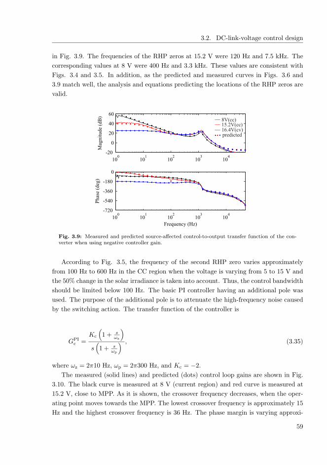
3.2. DC-link-voltage control design
in Fig. 3.9. The frequencies of the RHP zeros at 15.2 V were 120 Hz and 7.5 kHz. The
corresponding values at 8 V were 400 Hz and 3.3 kHz. These values are consistent with
Figs. 3.4 and 3.5. In addition, as the predicted and measured curves in Figs. 3.6 and
3.9 match well, the analysis and equations predicting the locations of the RHP zeros are
valid.
100
101
102
103
104
-20
0
20
40
60
Mag
nit
ude
(dB
)
100
101
102
103
104
-720
-540
-360
-180
0
Phas
e (d
eg)
Frequency (Hz)
predicted
8V(cc)
16.4V(cv)15.2V(cc)
Fig. 3.9: Measured and predicted source-affected control-to-output transfer function of the con-verter when using negative controller gain.
According to Fig. 3.5, the frequency of the second RHP zero varies approximately
from 100 Hz to 600 Hz in the CC region when the voltage is varying from 5 to 15 V and
the 50% change in the solar irradiance is taken into account. Thus, the control bandwidth
should be limited below 100 Hz. The basic PI controller having an additional pole was
used. The purpose of the additional pole is to attenuate the high-frequency noise caused
by the switching action. The transfer function of the controller is
GPIc =
Kc
(
1 + s
ωz
)
s(
1 + s
ωp
) , (3.35)
where ωz = 2π10 Hz, ωp = 2π300 Hz, and Kc = −2.
The measured (solid lines) and predicted (dots) control loop gains are shown in Fig.
3.10. The black curve is measured at 8 V (current region) and red curve is measured at
15.2 V, close to MPP. As it is shown, the crossover frequency decreases, when the oper-
ating point moves towards the MPP. The lowest crossover frequency is approximately 15
Hz and the highest crossover frequency is 36 Hz. The phase margin is varying approxi-
59
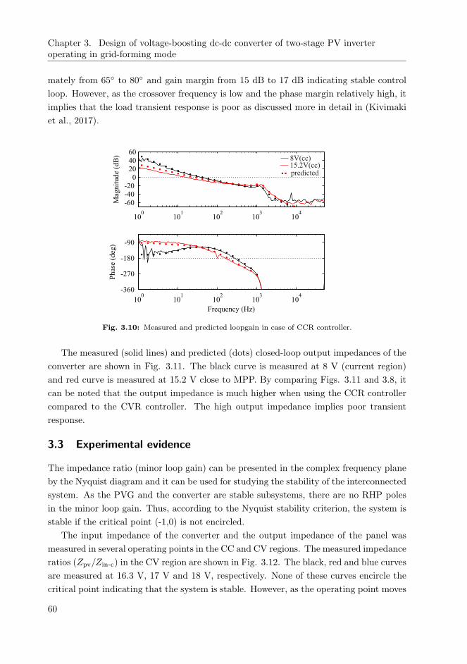
Chapter 3. Design of voltage-boosting dc-dc converter of two-stage PV inverteroperating in grid-forming mode
mately from 65 to 80 and gain margin from 15 dB to 17 dB indicating stable control
loop. However, as the crossover frequency is low and the phase margin relatively high, it
implies that the load transient response is poor as discussed more in detail in (Kivimaki
et al., 2017).
100
101
102
103
104
-60-40-20
0204060
Mag
nit
ude
(dB
)
100
101
102
103
104
-360
-270
-180
-90
Phas
e (d
eg)
Frequency (Hz)
predicted
8V(cc)15.2V(cc)
Fig. 3.10: Measured and predicted loopgain in case of CCR controller.
The measured (solid lines) and predicted (dots) closed-loop output impedances of the
converter are shown in Fig. 3.11. The black curve is measured at 8 V (current region)
and red curve is measured at 15.2 V close to MPP. By comparing Figs. 3.11 and 3.8, it
can be noted that the output impedance is much higher when using the CCR controller
compared to the CVR controller. The high output impedance implies poor transient
response.
3.3 Experimental evidence
The impedance ratio (minor loop gain) can be presented in the complex frequency plane
by the Nyquist diagram and it can be used for studying the stability of the interconnected
system. As the PVG and the converter are stable subsystems, there are no RHP poles
in the minor loop gain. Thus, according to the Nyquist stability criterion, the system is
stable if the critical point (-1,0) is not encircled.
The input impedance of the converter and the output impedance of the panel was
measured in several operating points in the CC and CV regions. The measured impedance
ratios (Zpv/Zin-c) in the CV region are shown in Fig. 3.12. The black, red and blue curves
are measured at 16.3 V, 17 V and 18 V, respectively. None of these curves encircle the
critical point indicating that the system is stable. However, as the operating point moves
60

3.3. Experimental evidence
100
101
102
103
104
-20
0
20
40
Mag
nit
ude
(dB
)
100
101
102
103
104
-90
-45
0
45
90
Phas
e (d
eg)
Frequency (Hz)
predicted
8V(cc)15.2V(cc)
Fig. 3.11: Measured and predicted closed-loop output impedances of the converter, when usingCCR controller.
closer to the MPP, the curve gets closer to the critical point. If the voltage would be
further decreased, the Nyquist contour would encircle the critical point into clockwise
direction meaning that the system would be unstable.
-1.4 -1.2 -1 -0.8 -0.6 -0.4 -0.2 0 0.2 0.4-6
-4
-2
0
2
4
6
Real
Imgin
ary
pv 16.3VV =
pv 17VV =
pv 18VV =
Fig. 3.12: The measured ratios of the impedances in complex plane when the operating pointmoves towards the MPP in CV region.
The time-domain behavior is demonstrated in Fig. 3.13, when using the CVR con-
61
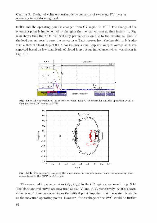
Chapter 3. Design of voltage-boosting dc-dc converter of two-stage PV inverteroperating in grid-forming mode
troller and the operating point is changed from CV region to MPP. The change of the
operating point is implemented by changing the the load current at time instant t1. Fig.
3.13 shows that the MOSFET will stay permanently on due to the instability. Even if
the load current goes to zero, the converter will not recover from the instability. It is also
visible that the load step of 0.4 A causes only a small dip into output voltage as it was
expected based on low magnitude of closed-loop output impedance, which was shown in
Fig. 3.13.
Time (10ms/div)
dcv 26V
18V
0V:
0V:
CVR
1t 2t
Unstable
pvv
dci 0.3A
0.7A:
0A:
Fig. 3.13: The operation of the converter, when using CVR controller and the operation point ischanged from CV region to MPP.
-1.4 -1.2 -1 -0.8 -0.6 -0.4 -0.2 0 0.2 0.4-0.5
-0.4
-0.3
-0.2
-0.1
0
0.1
0.2
0.3
0.4
0.5
Real
Imag
inar
y
pv 15.3VV =
pv 14VV =
Fig. 3.14: The measured ratios of the impedances in complex plane, when the operating pointmoves towards the MPP in CC region.
The measured impedance ratios (Zin-c/Zpv) in the CC region are shown in Fig. 3.14.
The black and red curves are measured at 15.3 V, and 14 V, respectively. As it is shown,
either one of these curves encircles the critical point implying that the system is stable
at the measured operating points. However, if the voltage of the PVG would be further
62
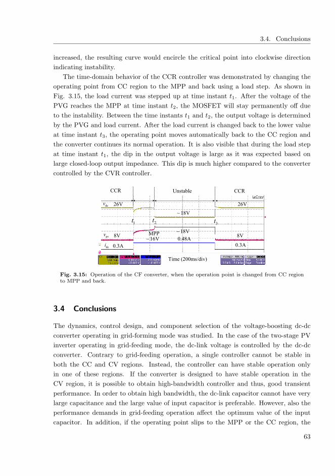
3.4. Conclusions
increased, the resulting curve would encircle the critical point into clockwise direction
indicating instability.
The time-domain behavior of the CCR controller was demonstrated by changing the
operating point from CC region to the MPP and back using a load step. As shown in
Fig. 3.15, the load current was stepped up at time instant t1. After the voltage of the
PVG reaches the MPP at time instant t2, the MOSFET will stay permanently off due
to the instability. Between the time instants t1 and t2, the output voltage is determined
by the PVG and load current. After the load current is changed back to the lower value
at time instant t3, the operating point moves automatically back to the CC region and
the converter continues its normal operation. It is also visible that during the load step
at time instant t1, the dip in the output voltage is large as it was expected based on
large closed-loop output impedance. This dip is much higher compared to the converter
controlled by the CVR controller.
Time (200ms/div)
dcv 26V 26V
8V
0.3A 0.3A
0.48A8V
16V:
18V:
18V:
CCR
MPP
1t 2t 3t
Unstable CCR
pvv
dci
Fig. 3.15: Operation of the CF converter, when the operation point is changed from CC regionto MPP and back.
3.4 Conclusions
The dynamics, control design, and component selection of the voltage-boosting dc-dc
converter operating in grid-forming mode was studied. In the case of the two-stage PV
inverter operating in grid-feeding mode, the dc-link voltage is controlled by the dc-dc
converter. Contrary to grid-feeding operation, a single controller cannot be stable in
both the CC and CV regions. Instead, the controller can have stable operation only
in one of these regions. If the converter is designed to have stable operation in the
CV region, it is possible to obtain high-bandwidth controller and thus, good transient
performance. In order to obtain high bandwidth, the dc-link capacitor cannot have very
large capacitance and the large value of input capacitor is preferable. However, also the
performance demands in grid-feeding operation affect the optimum value of the input
capacitor. In addition, if the operating point slips to the MPP or the CC region, the
63

Chapter 3. Design of voltage-boosting dc-dc converter of two-stage PV inverteroperating in grid-forming mode
converter will stay permanently unstable. The only way to continue stable operation is
to first decrease the load and then to reset the controller.
The clearest benefit of designing the converter to have stable operation in the CC
region is its ability to automatically recover after instability caused by moving the op-
erating point into the MPP or CV region. It was shown that the converter is able to
continue its normal operation right after the overload condition is over. However, the
control bandwidth must be limited to very low level due to the low-frequency RHP zero
in the control loop. Thus the transient performance is very poor. The performance could
be somewhat improved by using small capacitance value in the input capacitor. How-
ever, the selected value should be suitable for grid-feeding operation as well. The usage
of adaptive control methods is probably compulsory in practical implementations if the
converter is required to operate in the CC region, when operating in grid-forming mode.
It was also shown that the control-to-output dynamics of the dc-link-voltage controlled
converter can be described correctly either by the z-parameter or g-parameter model as
long as the output impedance of the PVG is taken into account in the model. If the
correct impedance ratio for impedance-based stability analysis is not known, it can be
found explicitly by selecting the z-parameter or g-parameter model, when designing the
controller for operation in the CC or CV region, respectively.
64
4 SATURATING GRID-FILTER INDUCTORS IN
THREE-PHASE PV INVERTER
In this chapter, a simulation model of the single-stage grid-connected three-phase PV
inverter having saturating L-filter inductors is developed. The developed model is used
for studying the effect of saturating filter inductors on the low-frequency and switching-
frequency current harmonics flowing into the grid. Also an equation for estimating the
peak value of the switching-frequency current ripple is presented. Finally, all the pre-
sented results are verified by measurements using a laboratory prototype.
4.1 Modeling
The main circuit of the single-stage grid-connected three-phase PV inverter is shown in
Fig. 4.1. As it was previously mentioned, it is common to use LCL-type filter as it
provides the same amount of attenuation in smaller size compared to L-filter. In this
thesis, it is assumed that the inverter-side inductor has varying inductance and the grid-
side inductor has constant inductance. As the focus is on the inverter-side inductor, the
CL-part is left out from the analysis. The L and CL-parts can be analyzed separately
if the inductance of the grid-filter inductor is high enough compared to the grid-side
inductance and the grid side inductor is linear. Usually this assumption is valid as the
inductance of the grid-filter inductor is selected to limit the maximum current ripple for
preventing excessive power losses, and the value of grid-side inductor can be much smaller
to obtain adequate attenuation at the switching frequency. If necessary, the linear CL
part can be added into the presented model.
The effect of grid-filter inductor saturation on the low-frequency harmonics was stud-
ied by comparing two cases: The three-phase PV inverter shown in Fig. 4.1 having linear,
i.e., constant valued-inductors and the same inverter having saturating inductors. The
parameters of the inverter are shown in Table 4.1. The maximum switching-frequency
current ripple was selected to be 10 % of the peak current, yielding an inductance of 2.5
mH in the linear case. The inductance of the saturating inductor is varying between 1
mH and 2.4 mH during the grid period. The saturating inductor was designed to have
wide inductance range in order to have clear effect on low-frequency harmonics. Only a
case of three individual inductors in each phase legs was studied.
65
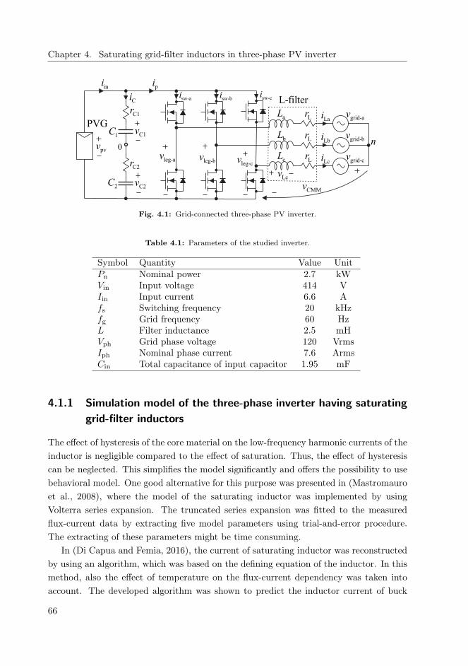
Chapter 4. Saturating grid-filter inductors in three-phase PV inverter
PVGaL
grid-av
grid-bv
grid-cv
n1C
L-filter
ini pi
sw-aisw-bi sw-ci
Ci
C1r
pvv
C2v
leg-av
Lai
Lbi
Lci
Lr
Lr
Lrleg-bvleg-cv
bL
cL
Lcv
CMMv
C2r
2C
C1v
0
Fig. 4.1: Grid-connected three-phase PV inverter.
Table 4.1: Parameters of the studied inverter.
Symbol Quantity Value UnitPn Nominal power 2.7 kWVin Input voltage 414 VIin Input current 6.6 Afs Switching frequency 20 kHzfg Grid frequency 60 HzL Filter inductance 2.5 mHVph Grid phase voltage 120 VrmsIph Nominal phase current 7.6 ArmsCin Total capacitance of input capacitor 1.95 mF
4.1.1 Simulation model of the three-phase inverter having saturating
grid-filter inductors
The effect of hysteresis of the core material on the low-frequency harmonic currents of the
inductor is negligible compared to the effect of saturation. Thus, the effect of hysteresis
can be neglected. This simplifies the model significantly and offers the possibility to use
behavioral model. One good alternative for this purpose was presented in (Mastromauro
et al., 2008), where the model of the saturating inductor was implemented by using
Volterra series expansion. The truncated series expansion was fitted to the measured
flux-current data by extracting five model parameters using trial-and-error procedure.
The extracting of these parameters might be time consuming.
In (Di Capua and Femia, 2016), the current of saturating inductor was reconstructed
by using an algorithm, which was based on the defining equation of the inductor. In this
method, also the effect of temperature on the flux-current dependency was taken into
account. The developed algorithm was shown to predict the inductor current of buck
66

4.1. Modeling
converter accurately, which was operating at switching frequency of 485 kHz . The main
drawback of the presented method is its complexity.
As the complete model of the three-phase inverter is complex, it is important that the
sub models of the grid-filter inductors are as simple as possible to prevent unnecessary
long simulation time. For this reason, neither of the previously mentioned models were
used. Instead, two different simulation models were developed, which were both based on
the measured current-inductance curve of the saturating inductor. In the first of these
two models the inductance-current data is included directly in the model, and in the
second model the flux-current data is calculated by integrating the current-inductance
data. The flux-current data is then included in the model as a table. Thus, extraction
of model parameters is not required in either of these models offering clear benefit. The
current-inductance curve is usually available as it is commonly measured to verify the
inductor design. Depending on the data provided by the manufacturer of the inductor
core, the dependency of the flux or inductance on current can also be calculated.
Usually the simulator-based model of the saturating inductor is implemented using a
controllable current source (Liu et al., 2012; Mastromauro et al., 2008; Ngo, 2002). In the
case of the three-phase inverter without a neutral conductor, the model will contain three
controllable current sources connected to the same circuit node. As this causes problems
for the solver of the simulator, usually a resistor is connected from the star point to
the center of the dc-link capacitors. Another option is to connect a resistor parallel to
some of the current sources, or a resistor parallel to each current sources. Depending on
the parameter values of the model, these additional resistors might affect too much the
simulation, causing incorrect simulation results. An example of such model can be found
from (Viinamaki, Jokipii and Suntio, 2015).
To avoid the problems caused by these additional resistors, the first of the two de-
veloped simulation models was implemented by solving the differential equations of the
inverter. As the impedances of the inductors are time-varying, the filter acts as an asym-
metric load for the switching bridge and therefore, solving the common-mode voltage
is challenging. For this reason, the model was transformed into alpha-beta frame. The
common-mode voltages cancel out, when this transformation is made. It should be noted
that this model can be used only for studying balanced three-phase system. The model
together with simulation results and measurements was presented in (Viinamaki, Jokipii
and Suntio, 2015). However, at the time the paper was written, it was not realized
that the measured inductance-current data is actually differential inductance. Thus, the
measurement data can be directly included into the model and it is not necessary to cal-
culate effective inductance as it was claimed. As the effective inductance was calculated
by using the measured data, the predicted switching-frequency ripple was higher than
in reality. Despite this error, the main conclusions made in the paper are correct and
67
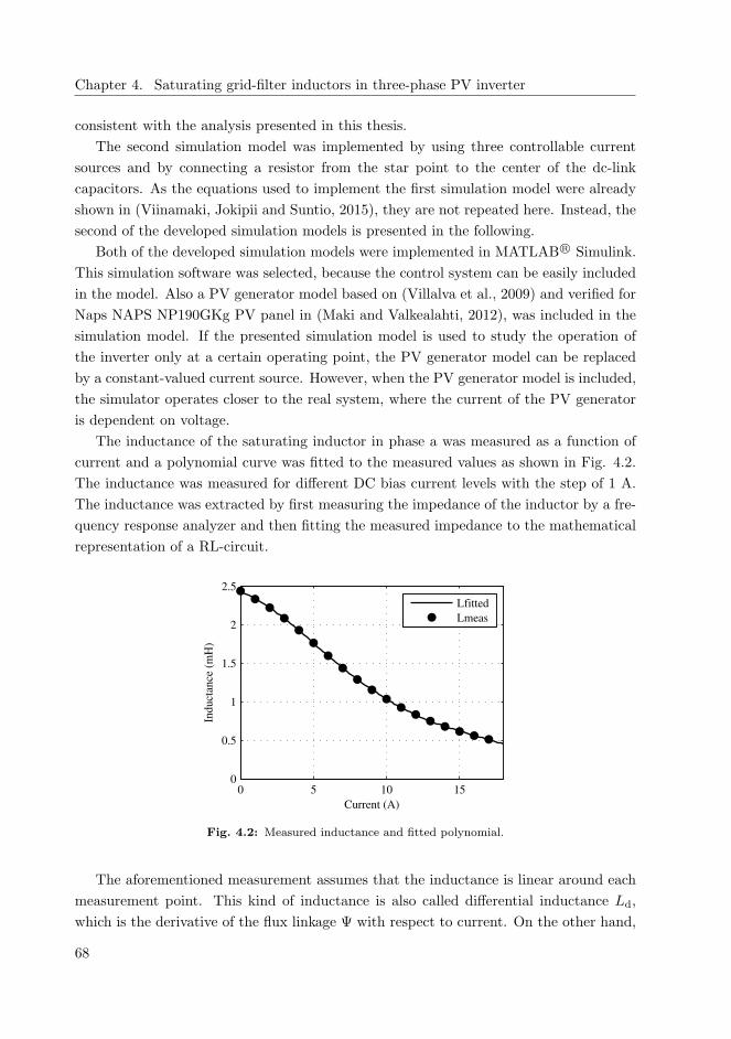
Chapter 4. Saturating grid-filter inductors in three-phase PV inverter
consistent with the analysis presented in this thesis.
The second simulation model was implemented by using three controllable current
sources and by connecting a resistor from the star point to the center of the dc-link
capacitors. As the equations used to implement the first simulation model were already
shown in (Viinamaki, Jokipii and Suntio, 2015), they are not repeated here. Instead, the
second of the developed simulation models is presented in the following.
Both of the developed simulation models were implemented in MATLAB R© Simulink.
This simulation software was selected, because the control system can be easily included
in the model. Also a PV generator model based on (Villalva et al., 2009) and verified for
Naps NAPS NP190GKg PV panel in (Maki and Valkealahti, 2012), was included in the
simulation model. If the presented simulation model is used to study the operation of
the inverter only at a certain operating point, the PV generator model can be replaced
by a constant-valued current source. However, when the PV generator model is included,
the simulator operates closer to the real system, where the current of the PV generator
is dependent on voltage.
The inductance of the saturating inductor in phase a was measured as a function of
current and a polynomial curve was fitted to the measured values as shown in Fig. 4.2.
The inductance was measured for different DC bias current levels with the step of 1 A.
The inductance was extracted by first measuring the impedance of the inductor by a fre-
quency response analyzer and then fitting the measured impedance to the mathematical
representation of a RL-circuit.
0 5 10 150
0.5
1
1.5
2
2.5
Current (A)
Induct
ance
(m
H)
Lfitted
Lmeas
Fig. 4.2: Measured inductance and fitted polynomial.
The aforementioned measurement assumes that the inductance is linear around each
measurement point. This kind of inductance is also called differential inductance Ld,
which is the derivative of the flux linkage Ψ with respect to current. On the other hand,
68
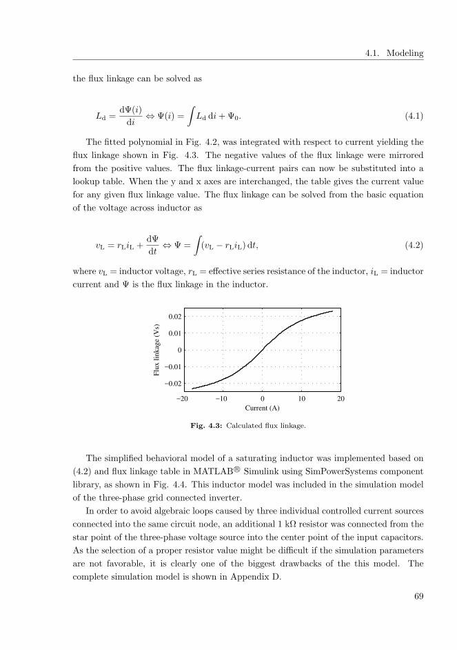
4.1. Modeling
the flux linkage can be solved as
Ld =dΨ(i)
di⇔ Ψ(i) =
∫
Ld di+Ψ0. (4.1)
The fitted polynomial in Fig. 4.2, was integrated with respect to current yielding the
flux linkage shown in Fig. 4.3. The negative values of the flux linkage were mirrored
from the positive values. The flux linkage-current pairs can now be substituted into a
lookup table. When the y and x axes are interchanged, the table gives the current value
for any given flux linkage value. The flux linkage can be solved from the basic equation
of the voltage across inductor as
vL = rLiL +dΨ
dt⇔ Ψ =
∫
(vL − rLiL) dt, (4.2)
where vL = inductor voltage, rL = effective series resistance of the inductor, iL = inductor
current and Ψ is the flux linkage in the inductor.
−20 −10 0 10 20
−0.02
−0.01
0
0.01
0.02
Current (A)
Flu
x l
inkag
e (V
s)
Fig. 4.3: Calculated flux linkage.
The simplified behavioral model of a saturating inductor was implemented based on
(4.2) and flux linkage table in MATLAB R© Simulink using SimPowerSystems component
library, as shown in Fig. 4.4. This inductor model was included in the simulation model
of the three-phase grid connected inverter.
In order to avoid algebraic loops caused by three individual controlled current sources
connected into the same circuit node, an additional 1 kΩ resistor was connected from the
star point of the three-phase voltage source into the center point of the input capacitors.
As the selection of a proper resistor value might be difficult if the simulation parameters
are not favorable, it is clearly one of the biggest drawbacks of the this model. The
complete simulation model is shown in Appendix D.
69
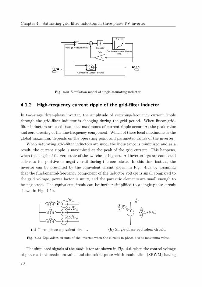
Chapter 4. Saturating grid-filter inductors in three-phase PV inverter
2
Conn21
Conn1
rL
Gain
v+-
Voltage Measurement
s
-+
Controlled Current Source
1
s
Integrator
1-D T(u)
Flux linkage-to-current lookup
table
Fig. 4.4: Simulation model of single saturating inductor.
4.1.2 High-frequency current ripple of the grid-filter inductor
In two-stage three-phase inverter, the amplitude of switching-frequency current ripple
through the grid-filter inductor is changing during the grid period. When linear grid-
filter inductors are used, two local maximums of current ripple occur: At the peak value
and zero crossing of the line-frequency component. Which of these local maximums is the
global maximum, depends on the operating point and parameter values of the inverter.
When saturating grid-filter inductors are used, the inductance is minimized and as a
result, the current ripple is maximized at the peak of the grid current. This happens,
when the length of the zero state of the switches is highest. All inverter legs are connected
either to the positive or negative rail during the zero state. In this time instant, the
inverter can be presented by the equivalent circuit shown in Fig. 4.5a by assuming
that the fundamental-frequency component of the inductor voltage is small compared to
the grid voltage, power factor is unity, and the parasitic elements are small enough to
be neglected. The equivalent circuit can be further simplified to a single-phase circuit
shown in Fig. 4.5b.
1L
2L
2L
ph2V
ph-0.5 2V
ph-0.5 2V
L1i
(a) Three-phase equivalent circuit.
hp
32
2V
1 20.5L L+
L1i
(b) Single-phase equivalent circuit.
Fig. 4.5: Equivalent circuits of the inverter when the current in phase a is at maximum value.
The simulated signals of the modulator are shown in Fig. 4.6, when the control voltage
of phase a is at maximum value and sinusoidal pulse width modulation (SPWM) having
70
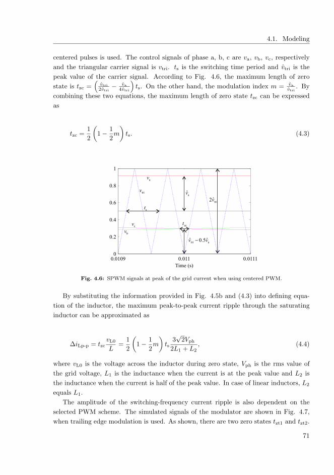
4.1. Modeling
centered pulses is used. The control signals of phase a, b, c are va, vb, vc, respectively
and the triangular carrier signal is vtri. ts is the switching time period and vtri is the
peak value of the carrier signal. According to Fig. 4.6, the maximum length of zero
state is tzc =(
vtri
2vtri− va
4vtri
)
ts. On the other hand, the modulation index m = va
vtri. By
combining these two equations, the maximum length of zero state tzc can be expressed
as
tzc =1
2
(
1− 1
2m
)
ts. (4.3)
0.0109 0.011 0.01110
0.2
0.4
0.6
0.8
1
Time (s)
st
av
tri aˆ ˆ0.5v v-
triv
av
bv
cv
triˆ2v
zct
Fig. 4.6: SPWM signals at peak of the grid current when using centered PWM.
By substituting the information provided in Fig. 4.5b and (4.3) into defining equa-
tion of the inductor, the maximum peak-to-peak current ripple through the saturating
inductor can be approximated as
∆iLp-p = tzcvL0L
=1
2
(
1− 1
2m
)
ts3√2Vph
2L1 + L2, (4.4)
where vL0 is the voltage across the inductor during zero state, Vph is the rms value of
the grid voltage, L1 is the inductance when the current is at the peak value and L2 is
the inductance when the current is half of the peak value. In case of linear inductors, L2
equals L1.
The amplitude of the switching-frequency current ripple is also dependent on the
selected PWM scheme. The simulated signals of the modulator are shown in Fig. 4.7,
when trailing edge modulation is used. As shown, there are two zero states tzt1 and tzt2.
71
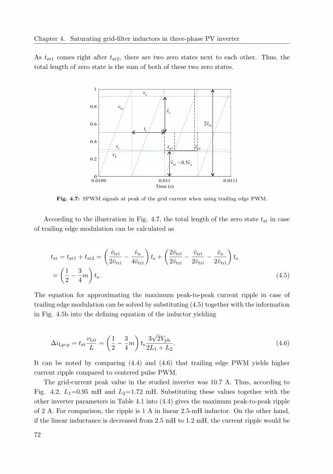
Chapter 4. Saturating grid-filter inductors in three-phase PV inverter
As tzt1 comes right after tzt2, there are two zero states next to each other. Thus, the
total length of zero state is the sum of both of these two zero states.
0.0109 0.011 0.01110
0.2
0.4
0.6
0.8
1
Time (s)
st
av
tri aˆ ˆ0.5v v-
av
triv
bv
cvzt1t zt2t
triˆ2v
Fig. 4.7: SPWM signals at peak of the grid current when using trailing edge PWM.
According to the illustration in Fig. 4.7, the total length of the zero state tzt in case
of trailing edge modulation can be calculated as
tzt = tzt1 + tzt2 =
(
vtri2vtri
− va4vtri
)
ts +
(
2vtri2vtri
− vtri2vtri
− va2vtri
)
ts
=
(
1
2− 3
4m
)
ts. (4.5)
The equation for approximating the maximum peak-to-peak current ripple in case of
trailing edge modulation can be solved by substituting (4.5) together with the information
in Fig. 4.5b into the defining equation of the inductor yielding
∆iLp-p = tztvL0L
=
(
1
2− 3
4m
)
ts3√2Vph
2L1 + L2. (4.6)
It can be noted by comparing (4.4) and (4.6) that trailing edge PWM yields higher
current ripple compared to centered pulse PWM.
The grid-current peak value in the studied inverter was 10.7 A. Thus, according to
Fig. 4.2, L1=0.95 mH and L2=1.72 mH. Substituting these values together with the
other inverter parameters in Table 4.1 into (4.4) gives the maximum peak-to-peak ripple
of 2 A. For comparison, the ripple is 1 A in linear 2.5-mH inductor. On the other hand,
if the linear inductance is decreased from 2.5 mH to 1.2 mH, the current ripple would be
72
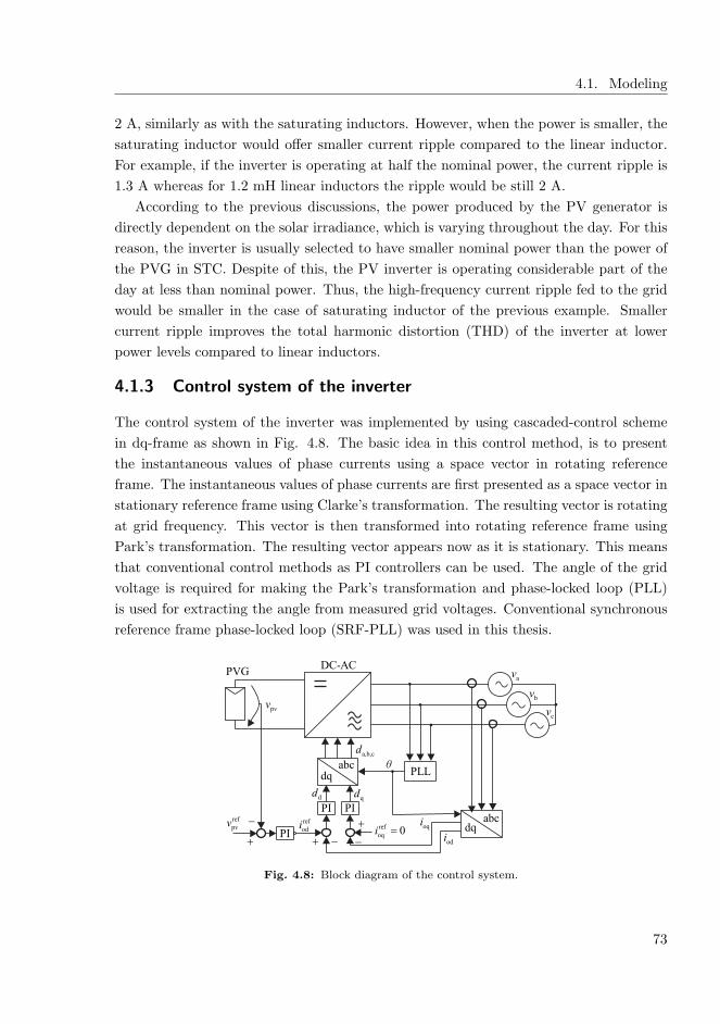
4.1. Modeling
2 A, similarly as with the saturating inductors. However, when the power is smaller, the
saturating inductor would offer smaller current ripple compared to the linear inductor.
For example, if the inverter is operating at half the nominal power, the current ripple is
1.3 A whereas for 1.2 mH linear inductors the ripple would be still 2 A.
According to the previous discussions, the power produced by the PV generator is
directly dependent on the solar irradiance, which is varying throughout the day. For this
reason, the inverter is usually selected to have smaller nominal power than the power of
the PVG in STC. Despite of this, the PV inverter is operating considerable part of the
day at less than nominal power. Thus, the high-frequency current ripple fed to the grid
would be smaller in the case of saturating inductor of the previous example. Smaller
current ripple improves the total harmonic distortion (THD) of the inverter at lower
power levels compared to linear inductors.
4.1.3 Control system of the inverter
The control system of the inverter was implemented by using cascaded-control scheme
in dq-frame as shown in Fig. 4.8. The basic idea in this control method, is to present
the instantaneous values of phase currents using a space vector in rotating reference
frame. The instantaneous values of phase currents are first presented as a space vector in
stationary reference frame using Clarke’s transformation. The resulting vector is rotating
at grid frequency. This vector is then transformed into rotating reference frame using
Park’s transformation. The resulting vector appears now as it is stationary. This means
that conventional control methods as PI controllers can be used. The angle of the grid
voltage is required for making the Park’s transformation and phase-locked loop (PLL)
is used for extracting the angle from measured grid voltages. Conventional synchronous
reference frame phase-locked loop (SRF-PLL) was used in this thesis.
PI PI
PI
PLLabc
abc
dq
dq
pvv
ref
oq 0i =
+
-ref
pvv ref
odi
+
+
- -
PVGDC-AC
oqi
odi
av
bv
cv
θ
a,b,cd
ddqd
Fig. 4.8: Block diagram of the control system.
73
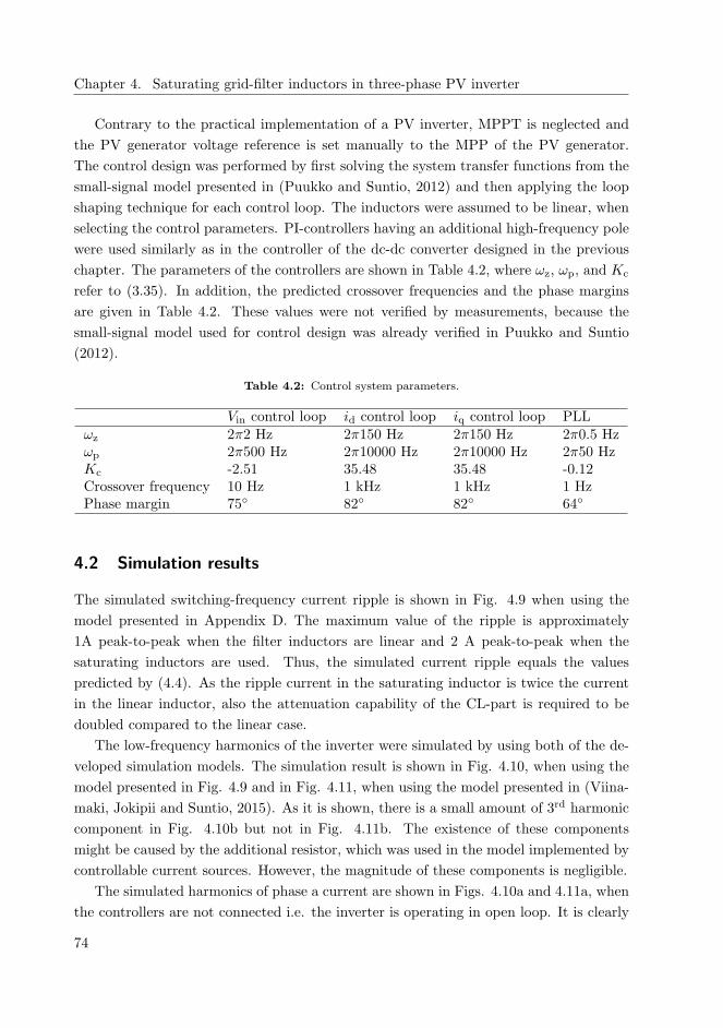
Chapter 4. Saturating grid-filter inductors in three-phase PV inverter
Contrary to the practical implementation of a PV inverter, MPPT is neglected and
the PV generator voltage reference is set manually to the MPP of the PV generator.
The control design was performed by first solving the system transfer functions from the
small-signal model presented in (Puukko and Suntio, 2012) and then applying the loop
shaping technique for each control loop. The inductors were assumed to be linear, when
selecting the control parameters. PI-controllers having an additional high-frequency pole
were used similarly as in the controller of the dc-dc converter designed in the previous
chapter. The parameters of the controllers are shown in Table 4.2, where ωz, ωp, and Kc
refer to (3.35). In addition, the predicted crossover frequencies and the phase margins
are given in Table 4.2. These values were not verified by measurements, because the
small-signal model used for control design was already verified in Puukko and Suntio
(2012).
Table 4.2: Control system parameters.
Vin control loop id control loop iq control loop PLLωz 2π2 Hz 2π150 Hz 2π150 Hz 2π0.5 Hzωp 2π500 Hz 2π10000 Hz 2π10000 Hz 2π50 HzKc -2.51 35.48 35.48 -0.12Crossover frequency 10 Hz 1 kHz 1 kHz 1 HzPhase margin 75 82 82 64
4.2 Simulation results
The simulated switching-frequency current ripple is shown in Fig. 4.9 when using the
model presented in Appendix D. The maximum value of the ripple is approximately
1A peak-to-peak when the filter inductors are linear and 2 A peak-to-peak when the
saturating inductors are used. Thus, the simulated current ripple equals the values
predicted by (4.4). As the ripple current in the saturating inductor is twice the current
in the linear inductor, also the attenuation capability of the CL-part is required to be
doubled compared to the linear case.
The low-frequency harmonics of the inverter were simulated by using both of the de-
veloped simulation models. The simulation result is shown in Fig. 4.10, when using the
model presented in Fig. 4.9 and in Fig. 4.11, when using the model presented in (Viina-
maki, Jokipii and Suntio, 2015). As it is shown, there is a small amount of 3rd harmonic
component in Fig. 4.10b but not in Fig. 4.11b. The existence of these components
might be caused by the additional resistor, which was used in the model implemented by
controllable current sources. However, the magnitude of these components is negligible.
The simulated harmonics of phase a current are shown in Figs. 4.10a and 4.11a, when
the controllers are not connected i.e. the inverter is operating in open loop. It is clearly
74
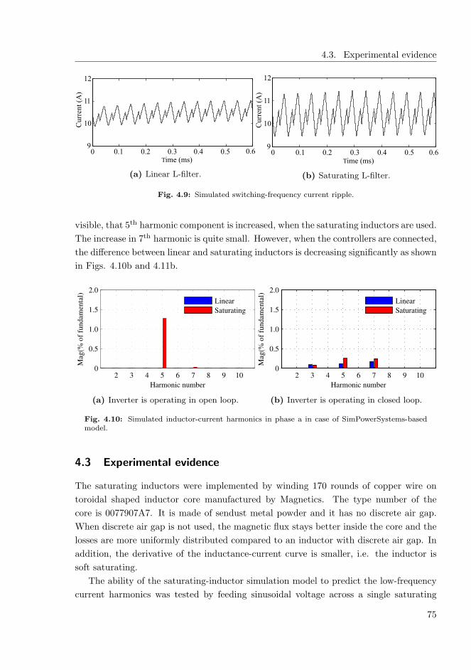
4.3. Experimental evidence
0 0.1 0.2 0.3 0.4 0.5 0.69
10
11
12
Time (ms)
Curr
ent
(A)
(a) Linear L-filter.
0 0.1 0.2 0.3 0.4 0.5 0.69
10
11
12
Time (ms)
Curr
ent
(A)
(b) Saturating L-filter.
Fig. 4.9: Simulated switching-frequency current ripple.
visible, that 5th harmonic component is increased, when the saturating inductors are used.
The increase in 7th harmonic is quite small. However, when the controllers are connected,
the difference between linear and saturating inductors is decreasing significantly as shown
in Figs. 4.10b and 4.11b.
2 3 4 5 6 7 8 9 100
0.5
1.0
1.5
2.0
Harmonic number
Mag
(% o
f fu
ndam
enta
l)
Linear
Saturating
(a) Inverter is operating in open loop.
2 3 4 5 6 7 8 9 100
0.5
1.0
1.5
2.0
Harmonic number
Mag
(% o
f fu
ndam
enta
l)
Linear
Saturating
(b) Inverter is operating in closed loop.
Fig. 4.10: Simulated inductor-current harmonics in phase a in case of SimPowerSystems-basedmodel.
4.3 Experimental evidence
The saturating inductors were implemented by winding 170 rounds of copper wire on
toroidal shaped inductor core manufactured by Magnetics. The type number of the
core is 0077907A7. It is made of sendust metal powder and it has no discrete air gap.
When discrete air gap is not used, the magnetic flux stays better inside the core and the
losses are more uniformly distributed compared to an inductor with discrete air gap. In
addition, the derivative of the inductance-current curve is smaller, i.e. the inductor is
soft saturating.
The ability of the saturating-inductor simulation model to predict the low-frequency
current harmonics was tested by feeding sinusoidal voltage across a single saturating
75
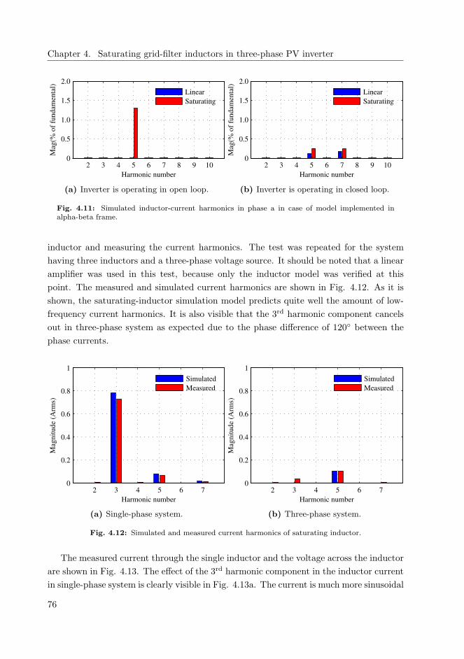
Chapter 4. Saturating grid-filter inductors in three-phase PV inverter
2 3 4 5 6 7 8 9 100
0.5
1.0
1.5
2.0
Harmonic number
Mag
(% o
f fu
ndam
enta
l)
Linear
Saturating
(a) Inverter is operating in open loop.
2 3 4 5 6 7 8 9 100
0.5
1.0
1.5
2.0
Harmonic number
Mag
(% o
f fu
ndam
enta
l)
Linear
Saturating
(b) Inverter is operating in closed loop.
Fig. 4.11: Simulated inductor-current harmonics in phase a in case of model implemented inalpha-beta frame.
inductor and measuring the current harmonics. The test was repeated for the system
having three inductors and a three-phase voltage source. It should be noted that a linear
amplifier was used in this test, because only the inductor model was verified at this
point. The measured and simulated current harmonics are shown in Fig. 4.12. As it is
shown, the saturating-inductor simulation model predicts quite well the amount of low-
frequency current harmonics. It is also visible that the 3rd harmonic component cancels
out in three-phase system as expected due to the phase difference of 120 between the
phase currents.
2 3 4 5 6 70
0.2
0.4
0.6
0.8
1
Harmonic number
Mag
nit
ude
(Arm
s)
Simulated
Measured
(a) Single-phase system.
2 3 4 5 6 70
0.2
0.4
0.6
0.8
1
Harmonic number
Mag
nit
ude
(Arm
s)
Simulated
Measured
(b) Three-phase system.
Fig. 4.12: Simulated and measured current harmonics of saturating inductor.
The measured current through the single inductor and the voltage across the inductor
are shown in Fig. 4.13. The effect of the 3rd harmonic component in the inductor current
in single-phase system is clearly visible in Fig. 4.13a. The current is much more sinusoidal
76
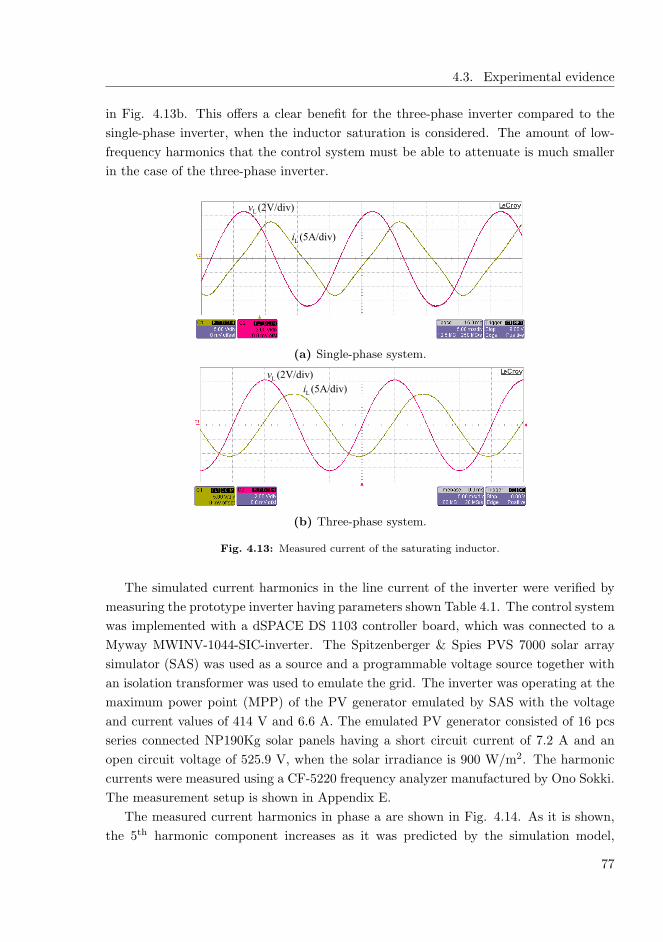
4.3. Experimental evidence
in Fig. 4.13b. This offers a clear benefit for the three-phase inverter compared to the
single-phase inverter, when the inductor saturation is considered. The amount of low-
frequency harmonics that the control system must be able to attenuate is much smaller
in the case of the three-phase inverter.
L (2V/div)v
L (5A/div)i
(a) Single-phase system.
L (5A/div)i
L (2V/div)v
(b) Three-phase system.
Fig. 4.13: Measured current of the saturating inductor.
The simulated current harmonics in the line current of the inverter were verified by
measuring the prototype inverter having parameters shown Table 4.1. The control system
was implemented with a dSPACE DS 1103 controller board, which was connected to a
Myway MWINV-1044-SIC-inverter. The Spitzenberger & Spies PVS 7000 solar array
simulator (SAS) was used as a source and a programmable voltage source together with
an isolation transformer was used to emulate the grid. The inverter was operating at the
maximum power point (MPP) of the PV generator emulated by SAS with the voltage
and current values of 414 V and 6.6 A. The emulated PV generator consisted of 16 pcs
series connected NP190Kg solar panels having a short circuit current of 7.2 A and an
open circuit voltage of 525.9 V, when the solar irradiance is 900 W/m2. The harmonic
currents were measured using a CF-5220 frequency analyzer manufactured by Ono Sokki.
The measurement setup is shown in Appendix E.
The measured current harmonics in phase a are shown in Fig. 4.14. As it is shown,
the 5th harmonic component increases as it was predicted by the simulation model,
77
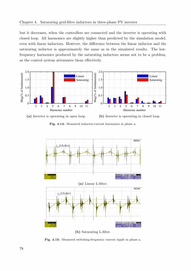
Chapter 4. Saturating grid-filter inductors in three-phase PV inverter
but it decreases, when the controllers are connected and the inverter is operating with
closed loop. All harmonics are slightly higher than predicted by the simulation model,
even with linear inductors. However, the difference between the linear inductor and the
saturating inductor is approximately the same as in the simulated results. The low-
frequency harmonics produced by the saturating inductors seems not to be a problem,
as the control system attenuates them effectively.
2 3 4 5 6 7 8 9 10 110
0.5
1.0
1.5
2.0
Harmonic number
Mag
(% o
f fu
ndam
enta
l)
Linear
Saturating
(a) Inverter is operating in open loop.
2 3 4 5 6 7 8 9 10 110
0.5
1.0
1.5
2.0
Harmonic number
Mag
(% o
f fu
ndam
enta
l)
Linear
Saturating
(b) Inverter is operating in closed loop.
Fig. 4.14: Measured inductor-current harmonics in phase a.
La (1A/div)i
(a) Linear L-filter.
La (1A/div)i
(b) Saturating L-filter.
Fig. 4.15: Measured switching-frequency current ripple in phase a.
78
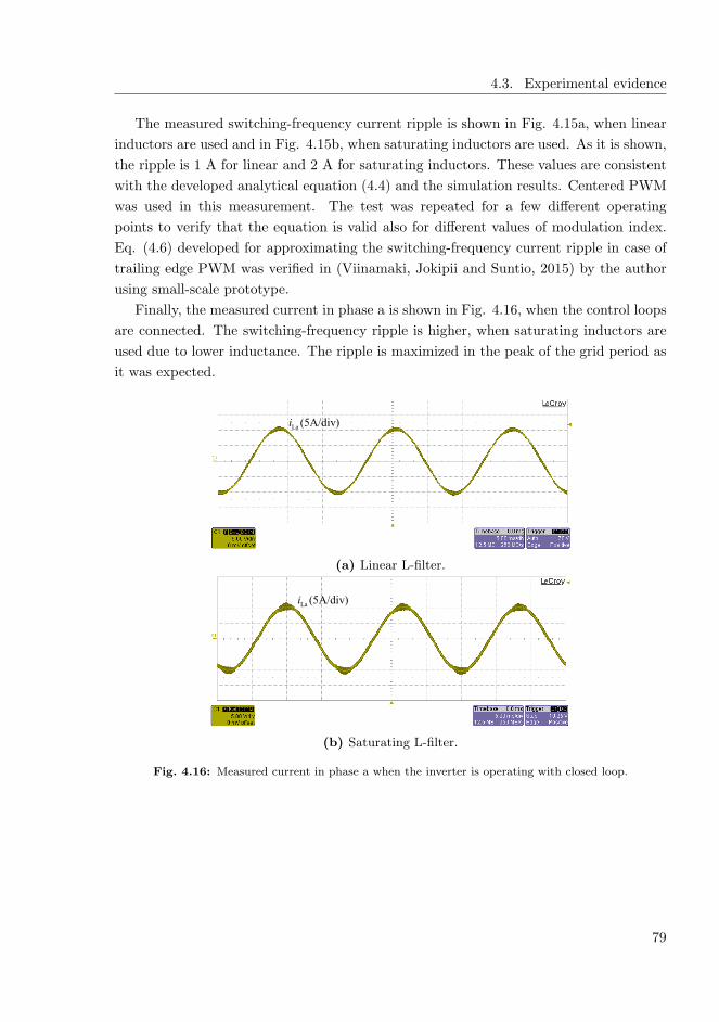
4.3. Experimental evidence
The measured switching-frequency current ripple is shown in Fig. 4.15a, when linear
inductors are used and in Fig. 4.15b, when saturating inductors are used. As it is shown,
the ripple is 1 A for linear and 2 A for saturating inductors. These values are consistent
with the developed analytical equation (4.4) and the simulation results. Centered PWM
was used in this measurement. The test was repeated for a few different operating
points to verify that the equation is valid also for different values of modulation index.
Eq. (4.6) developed for approximating the switching-frequency current ripple in case of
trailing edge PWM was verified in (Viinamaki, Jokipii and Suntio, 2015) by the author
using small-scale prototype.
Finally, the measured current in phase a is shown in Fig. 4.16, when the control loops
are connected. The switching-frequency ripple is higher, when saturating inductors are
used due to lower inductance. The ripple is maximized in the peak of the grid period as
it was expected.
La (5A/div)i
(a) Linear L-filter.
La (5A/div)i
(b) Saturating L-filter.
Fig. 4.16: Measured current in phase a when the inverter is operating with closed loop.
79

Chapter 4. Saturating grid-filter inductors in three-phase PV inverter
4.4 Conclusions
The effect of inductor saturation on the harmonic currents produced by a grid-connected
three-phase PV inverter was studied by simulations and measurements. The proposed
model was shown to be accurate enough in predicting current harmonics caused by the
saturating inductors. It was shown that the saturating L-filter inductor produces 5th and
7th harmonics in the line current, when the inverter is operating with open loop. These
low-frequency harmonics are effectively attenuated when the control loops are closed.
The conventional control method having basic PI controllers in the dq domain seems to
offer adequate attenuation for these harmonics. Thus, the appearance of low-frequency
harmonics is not limiting the use of saturating inductors in the studied case.
An analytical equation was proposed for evaluating the maximum magnitude of the
switching-frequency current ripple in the case of saturating inductors. The proposed
equation differs from the models presented in the literature in that the inductor saturation
was taken into account. The accuracy of the equation was verified by using a 2.7 kW
prototype and comparing the ripple of saturating and linear L-filter inductors. The
inductance value of the saturating inductor was selected to be the same as in the linear
inductor at low current level. In this case, the maximum current ripple is higher in the
saturating inductor compared to linear inductor. When considering LCL-filter having the
aforementioned L-filter as the switching bridge-side inductor, the attenuation capability
of the CL-part must be higher, when saturating inductor is used.
It was also observed that as the magnitude of the switching-frequency current ripple
is affected by the inductance in all three phases, the effect of saturation is not as high as
might be expected by just considering a single inductor. If a linear inductor producing
certain maximum amplitude of current ripple is compared with a saturating inductor
offering the same current ripple, the latter option would offer smaller ripple and THD
at lower power level. This would be advantageous in PV plants, where the inverter
operates for significant part of the time below the maximum power rating. Thus, inductor
saturation can be applied for minimizing the inductor size or the low-power current ripple.
80

5 CONCLUSIONS
5.1 Final conclusions
The component sizing and control design of the voltage-boosting dc-dc converter oper-
ating as a part of single-stage single-phase PV inverter was studied. The operation in
grid-feeding and grid-forming modes were both investigated separately. The dc-ac in-
verter was left out from the analysis as the focus was on the dc-dc converter. The load
of the dc-dc converter was modeled as constant voltage sink in the case of grid-feeding
mode and as constant current sink in the case of grid-forming mode.
First, the design of the dc-dc converter was studied by assuming grid-feeding opera-
tion. Two interfacing converters were designed for a single 190 W PV panel to study the
component sizing. In the first converter, the maximum input current of the converter was
calculated by dividing the nominal power of the converter by the minimum input voltage.
As this method originates from the systems having voltage-type sources, it was named
as conventional design method. In the second converter, the maximum input current
was assumed to equal the maximum SC current of the PV panel. Other major difference
between these two designs was, that the power losses of the diode were calculated in the
minimum input voltage condition in the case of conventional design, and at the MPP
in the case of the modified design. According to the investigations, using the modified
design method instead of the conventional one in case of wide input-voltage range yields
smaller inductor core, smaller heat sink of the MOSFET, smaller input capacitor and
more even temperature distribution.
By investigating the datasheets of the commercial PV inverters, it was noticed that
it is common to use conventional design method in the case of narrow input voltage
range, yielding reasonably small input current. In the case of high input voltage range,
the maximum input current is selected to be smaller than the value resulting from the
conventional design method. Thus, it seems that the manufacturers of the PV inverters
are familiar with the aforementioned issues. However, the fact that conventional design
method yields oversized components in the case of wide input-voltage range, needs to be
mentioned also in the design manuals for interfacing converters.
A small-signal model of voltage-boosting converter having dc-link-voltage feedforward
was developed. Grid-feeding operation was assumed in this study. The developed model
81
Chapter 5. Conclusions
was used to study the effect of feedforward on the attenuation of double-line-frequency
voltage ripple from the dc-link to the PVG. It was shown, that the highest attenuation
is obtained by using as high dc-link voltage as possible, minimized parasitic resistances
of the switches and inductor and using synchronous instead of diode-switched converter.
Even if open-loop operation was assumed in this study, the presented results can be
applied also for closed-loop operation. In this case, the attenuation of the double-line-
frequency voltage ripple would be a sum of the effects of input voltage controller and the
dc-link-voltage feedforward.
Next, the design of the dc-dc converter was studied by assuming grid-forming opera-
tion. Contrary to grid-feeding operation, a single controller cannot be stable both in CC
and CV regions. Instead, the controller can have stable operation only in one of these
regions. If the converter is designed to have stable operation in the CV region, it is pos-
sible to obtain high-bandwidth controller and good transient performance. In order to
obtain high bandwidth, the dc-link capacitor cannot have very large capacitance, and the
large value of input capacitor is preferable. However, also the performance requirements
in grid-feeding operation affect the optimum value of the input capacitor. In addition,
if the operating point slips to MPP or CC region, the converter will stay permanently
unstable. The only way to continue stable operation is to first decrease the load and then
to reset the controller.
The clearest benefit of designing the converter to have stable operation in the CC
region is its ability to automatically recover after instability caused by moving the op-
erating point into the MPP or CV region. It was shown that the converter is able to
continue its normal operation right after the overload condition is over. However, the
control bandwidth must be limited to very low level due to the low-frequency RHP zero
in the control loop. Thus, the transient performance would be very poor.
Finally, the effect of inductor saturation on the harmonic currents produced by a grid-
connected three-phase PV inverter was studied by simulations and measurements. The
proposed model was shown to be accurate enough in predicting current harmonics caused
by saturating inductors. It was shown that the saturating L-filter inductor produces 5th
and 7th harmonics in the line current, when the inverter is operating with open loop.
These low-frequency harmonics are effectively attenuated, when the control loops are
closed. The conventional control method having basic PI controllers in the dq domain
seems to offer adequate attenuation for these harmonics. Thus, the appearance of low-
frequency harmonics is not limiting the use of saturating inductors.
5.2 Future research topics
The following research topics provide an interesting continuation for the research pre-
sented in this thesis.
82

5.2. Future research topics
• As it was shown, robust control design with adequate dynamics is very hard to
obtain, when designing a conventional voltage-boosting dc-dc converter for stable
operation in the CC region for grid-forming operation. On the other hand, if the
converter is designed for stable operation in the CV region, the controller will
not recover without reset when the operation point has slipped to the MPP or
into the CC region. Thus, it would be interesting to study the applicability of
other topologies for this application. The modified superbuck-converter reported
in Agamy et al. (2013), might be a good alternative, because the low-frequency
RHP zero limiting the control bandwidth in the CC region can be eliminated by
selecting the input-terminal capacitors properly (Leppaaho and Suntio, 2011).
• The effect of inductor saturation on the harmonic currents produced by a grid-
connected three-phase PV inverter was studied by simulations and measurements
in this thesis. It was concluded that the appearance of low-frequency harmonics
is not limiting the use of saturating inductors. However, the study should be
extended to higher power levels to be certain that the result is applicable also in
those cases. As the control bandwidth is lower in higher power level devices, the
ability to attenuate the low-frequency harmonics is not that good and it might
cause problems.
• The study on saturating inductors in grid-connected three-phase PV inverter was
focusing only on the mitigation of low-frequency current harmonics and prediction
of switching-frequency current harmonics. Also the effect of increased switching-
frequency ripple on the size of the electromagnetic interference (EMI) filters should
be studied. It is not yet answered if the saturating grid filter has too many negative
effects on increased EMI noise (or filter size), power losses and heat for it to be
used in practice.
• In this thesis, the component sizing of voltage-boosting dc-dc converter was studied
separately when operating in grid-feeding and grid-forming modes. It would be
interesting to continue the research by designing a two-stage PV inverter having
minimized size and cost and able to operate in grid-forming, grid-feeding and grid-
supporting operating modes. The results presented in this thesis could be utilized
for this kind of study.
• Energy storage unit seems to be essential, when the share of intermittent renewable
power generation increases. Cheap and ecological ways to store the electrical energy
must be developed. Using of different technology for short-term storage and long-
term storage might be economically profitable also in the future.
83

REFERENCES
REFERENCES
Agamy, M. S., Chi, S., Elasser, A., Harfman-Todorovic, M., Jiang, Y., Mueller, F. and
Tao, F. (2013). A high-power-density DC-DC converter for distributed PV architec-
tures, IEEE J. Photovolt. 3(2): 791–798.
Bacha, S., Picault, D., Burger, B., Etxeberria-Otadui, I. and Martins, J. a. (2015).
Photovoltaics in microgrids: an overview of grid integration and energy management
aspects, IEEE Ind. Electron. Mag. 9(1): 33–46.
Beres, R. N., Wang, X., Blaabjerg, F., Liserre, M. and Bak, C. L. (2016). Optimal de-
sign of high-order passive-damped filters for grid-connected applications, IEEE Trans.
Power Electron. 31(3): 2083–2098.
Blaabjerg, F., Chen, Z. and Kjaer, S. B. (2004). Power electronics as efficient interface in
dispersed power generation systems, IEEE Trans. Power Electron. 19(5): 1184–1194.
Bose, B. K. (2010). Global warming: energy, environmental pollution, and the impact of
power electronics, IEEE Ind. Electron. Mag. 4(1): 6–17.
Bossche, A. V. and Valchev, V. C. (2005). Inductors and transformers for power elec-
tronics, Taylor & Francis.
Boztepe, M., Guinjoan, F., Velasco-Quesada, G., Silvestre, S., Chouder, A. and Karatepe,
E. (2014). Global MPPT scheme for photovoltaic string inverters based on restricted
voltage window search algorithm, IEEE Trans. Ind. Electron. 61(7): 3302–3312.
Burger, B. and Ruther, R. (2006). Inverter sizing of grid-connected photovoltaic systems
in the light of local solar resource distribution characteristics and temperature, Solar
Energy 80(1): 32–45.
Cai, H., Xiang, J. and Wei, W. (2016). Modelling, analysis and control design of a two-
stage photovoltaic generation system, IET Renewable Power Generation 10(8): 1195–
1203.
Channegowda, P. and John, V. (2010). Filter optimization for grid interactive voltage
source inverters, IEEE Trans. Ind. Electron. 57(12): 4106–4114.
Chen, S., Li, P., Brady, D. and Lehman, B. (2011). Optimum inverter sizing in consider-
ation of irradiance pattern and PV incentives, Applied Power Electronics Conference
and Exposition (APEC), pp. 982–988.
Chen, S., Li, P., Brady, D. and Lehman, B. (2013). Determining the optimum grid-
connected photovoltaic inverter size, Solar Energy 87(1): 96–116.
85

REFERENCES
Cuk, S. and Middlebrook, R. D. (1977). A general unified approach to modelling switching
DC-to-DC converters in discontinuous conduction mode, Power Electronics Specialists
Conference, pp. 36–57.
Danyali, S., Hosseini, S. H., Gharehpetian, G. B. and Member, S. (2014). New extendable
single-stage multi-input DC - DC/AC boost converter, IEEE Trans. Power Electron.
29(2): 775–788.
Datasheet of ABB string inverter PRO-33.0 (2016).
URL: https://library.e.abb.com/public/619bf289f98f44d2be6cbeaaf27761ad/
17315 String inverter PRO-33.0-TL-OUTD flyer EN 3AUA0000164968 RevF.pdf
[Date accessed: 27.12.2016]
Datasheet of Sunny Tripower 10000TLEE-JP (2016).
URL: http://files.sma.de/dl/22279/STP10000TLEE-JP-10-11-MOW-DEN1651-
V31web.pdf [Date accessed: 27.12.2016]
Datasheet of Vacon 8000 solar inverter series (2014).
URL: http://www.vacon.com/ImageVaultFiles/id 3122/cf 2/Vacon-8000-Solar-
Brochure-BC00414F-EN.PDF?634852861613100000/ [Date accessed: 27.12.2016]
Di Capua, G. and Femia, N. (2016). A novel method to predict the real operation
of ferrite inductors with moderate saturation in switching power supply applications,
IEEE Trans. Power Electron. 31(3): 2456–2464.
Donescu, V., Charette, A., Yao, Z. and Rajagopalan, V. (1999). Modeling and simula-
tion of saturated induction motors in phase quantities, IEEE Trans. Energy Convers.
14(3): 386–393.
Erickson, R. W. and Maksimovic, D. (2006). Fundamentals of power electronics, Springer.
Esram, T. and Chapman, P. L. (2007). Comparison of photovoltaic array maximum
power point tracking techniques, IEEE Trans. Energy Convers. 22(2): 439–449.
Femia, N., Petrone, G., Spagnuolo, G. and Vitelli, M. (2009). A technique for improving
P&O MPPT performances of double-stage grid-connected photovoltaic systems, IEEE
Trans. Ind. Electron. 56(11): 4473–4482.
Forouzesh, M., Siwakoti, Y. P., Gorji, S. a., Blaabjerg, F. and Lehman, B. (2017). Step-up
DC-DC Converters: a comprehensive review of voltage-boosting techniques, topologies,
and applications, IEEE Trans. Power Electron. 32(12): 9143–9178.
Grainger, B. M., Reed, G. F., Sparacino, A. R. and Lewis, P. T. (2014). Power electronics
for grid-scale energy storage, Proc. IEEE 102(6): 1000–1013.
86

REFERENCES
Gu, B., Dominic, J., Zhang, J., Zhang, L., Chen, B. and Lai, J.-S. (2014). Control
of electrolyte-free microinverter with improved MPPT performance and grid current
quality, Applied Power Electronics Conference and Exposition (APEC), pp. 1788–1792.
Ho, C. N.-M., Breuninger, H., Pettersson, S., Escobar, G. and Canales, F. (2013). A
comparative performance study of an interleaved boost converter using commercial Si
and SiC diodes for PV applications, IEEE Trans. Power Electron. 28(1): 289–299.
Ho, C. N.-m., Breuninger, H., Pettersson, S., Escobar, G., Serpa, L. A. and Coccia, A.
(2012). Practical design and implementation procedure of an interleaved boost con-
verter using SiC diodes for PV applications, IEEE Trans. Power Electron. 27(6): 2835–
2845.
Hu, H., Harb, S., Kutkut, N., Batarseh, I. and Shen, Z. J. (2013). A Review of power
decoupling techniques for microinverters with three different decoupling capacitor lo-
cations in PV systems, IEEE Trans. Power Electron. 28(6): 2711–2726.
International Energy Agency (2016a). Key world energy statistics 2016, Technical
report, International Energy Agency.
URL: https://www.iea.org/publications/freepublications/publication/KeyWorld2016.pdf
[Date accessed: 30.9.2016]
International Energy Agency (2016b). Snapshot of global photovoltaic markets 2015,
Technical report, International Energy Agency.
URL: http://www.iea-pvps.org/ [Date accessed: 23.9.2016]
Karshenas, H. R. and Saghafi, H. (2006). Basic criteria in designing LCL filters for grid
connected converters, International Symposium on Industrial Electronics, pp. 1996–
2000.
Kazimierczuk, M. and Starman, L. (1999). Dynamic performance of PWM DC-DC
boost converter with input voltage feedforward control, IEEE Trans. Circuits Syst. I,
Fundam. Theory Appl. 46(12): 1473–1481.
Kivimaki, J., Kolesnik, S., Sitbon, M., Suntio, T. and Kuperman, A. (2017). De-
sign guidelines for multi-loop perturbative maximum power point tracking algorithms,
IEEE Trans. Power Electron. PP(99): 1–1.
Kjaer, S. B., Pedersen, J. K. and Blaabjerg, F. (2005). A review of single-phase grid-
connected inverters for photovoltaic modules, IEEE Trans. Ind. Appl. 41(5): 1292–
1306.
87
REFERENCES
Konstantopoulos, G. C. and Alexandridis, A. T. (2013). Non-linear voltage regulator
design for DC/DC boost converters used in photovoltaic applications: analysis and
experimental results, IET Renewable Power Generation 7(3): 296–308.
Kouro, S., Leon, J. I., Vinnikov, D. and Franquelo, L. G. (2015). Grid-connected photo-
voltaic systems: an overview of recent research and emerging PV converter technology,
IEEE Ind. Electron. Mag. 9(1): 47–61.
Koutroulis, E. and Blaabjerg, F. (2011). Methods for the optimal design of grid-connected
PV inverters, International Journal of Renewable Energy Research 1(2): 54–64.
Lang, Y., Xu, D., S. R., H. and Ma, H. (2005). A novel design method of LCL type
utility interface for three-phase voltage source rectifier, Power Electronics Specialists
Conference (PESC), pp. 313–317.
Leppaaho, J. and Suntio, T. (2011). Dynamic characteristics of current-fed superbuck
converter, IEEE Trans. Power Electron. 26(1): 200–209.
Liserre, M., Blaabjerg, F. and Dell’Aquila, A. (2004). Step-by-step design procedure
for a grid-connected three-phase PWM voltage source converter, Int. J. Electron.
91(8): 445–460.
Liserre, M., Blaabjerg, F. and Hansen, S. (2005). Design and control of an LCL -filter-
based tree-phase active rectifier, IEEE Trans. Ind. Appl. 41(5): 1281–1291.
Liu, Z., Abou-Alfotouh, A. and Wilkowski, M. (2012). Nonlinear inductor modeling for
power converter, Applied Power Electronics Conference and Exposition (APEC), Ieee,
pp. 1868–1871.
Luoma, J., Kleissl, J. and Murray, K. (2012). Optimal inverter sizing considering cloud
enhancement, Solar Energy 86(1): 421–429.
Maki, A. and Valkealahti, S. (2012). Power losses in long string and parallel-connected
short strings of series-connected silicon-based photovoltaic modules due to partial shad-
ing conditions, IEEE Trans. Energy Convers. 27(1): 173–183.
Mastromauro, R. A. (2014). Voltage control of a grid-forming converter for an AC
microgrid : a real case study, Renewable Power Generation Conference (RPG), pp. 1–
6.
Mastromauro, R. A., Liserre, M. and Dell’Aquila, A. (2008). Study of the effects of
inductor nonlinear behavior on the performance of current controllers for single-phase
PV grid converters, IEEE Trans. Ind. Electron. 55(5): 2043–2052.
88

REFERENCES
Mayer, J. N., Philipps, S., Hussein, N. S., Schlegl, T. and Senkpiel, C. (2015). Current
and future cost of photovoltaics: long-term scenarios for market development, system
prices and LCOE of utility-scale PV systems, Technical report, Fraunhofer-Institute
for Solar Energy Systems.
Messo, T., Jokipii, J., Puukko, J. and Suntio, T. (2014). Determining the value of
DC-link capacitance to ensure stable operation of a three-phase photovoltaic inverter,
IEEE Trans. Power Electron. 29(2): 665–673.
Messo, T., Jokipii, J. and Suntio, T. (2012). Steady-state and dynamic properties of
boost-power-stage converter in photovoltaic applications, International Symposium on
Power Electronics for Distributed Generation Systems (PEDG) pp. 34–40.
Middlebrook, R. (1978). Design techniques for preventing input-filter oscillations
in switched-mode regulators, National Solid-State Power Conversion Conference,
pp. 153–168.
Middlebrook, R. D. (1988). Small-signal modeling of pulse-width modulated switched-
mode power converters, Proc. IEEE 76(4): 343–354.
Mirzahosseini, R. and Tahami, F. (2012). A lifetime improved single phase grid connected
photovoltaic inverter, Power Electronics and Drive Systems Technology (PEDSTC),
pp. 234–238.
Mondol, J. D., Yohanis, Y. G. and Norton, B. (2006). Optimal sizing of array and inverter
for grid-connected photovoltaic systems, Solar Energy 80(12): 1517–1539.
Muhlethaler, J., Schweizer, M., Blattmann, R., Kolar, J. W. and Ecklebe, A. (2013).
Optimal design of LCL harmonic filters for three-phase PFC rectifiers, IEEE Trans.
Power Electron. 28(7): 3114–3125.
Nandi, S. (2004). A detailed model of induction machines with saturation extendable for
fault analysis, IEEE Trans. Ind. Appl. 40(5): 1302–1309.
Neves, F. A. S., Carrasco, M., Mancilla-David, F., Azevedo, G. M. S. and Santos, V. S.
(2016). Unbalanced grid fault ride-through control for single-stage photovoltaic invert-
ers, IEEE Trans. Power Electron. 31(4): 3338–3347.
Ngo, K. (2002). Subcircuit modeling of magnetic cores with hysteresis in PSpice, IEEE
Trans. Aerosp. Electron. Syst. 38(4): 1425–1434.
Notton, G., Lazarov, V. and Stoyanov, L. (2010). Optimal sizing of a grid-connected
PV system for various PV module technologies and inclinations, inverter efficiency
characteristics and locations, Renewable Energy 35(2): 541–554.
89

REFERENCES
Nousiainen, L., Puukko, J., Maki, A., Messo, T., Huusari, J., Jokipii, J., Viinamaki, J.,
Lobera, D. T., Valkealahti, S. and Suntio, T. (2013). Photovoltaic generator as an input
source for power electronic converters, IEEE Trans. Power Electron. 28(6): 3028–3038.
Pan, D., Ruan, X., Bao, C., Li, W. and Wang, X. (2014). Magnetic integration of the
LCL filter in grid-connected inverters, IEEE Trans. Power Electron. 29(4): 1573–1578.
Perdigao, M. S., Alonso, J. M., Dalla Costa, M. A. and Saraiva, E. S. (2008). A vari-
able inductor MATLAB/simulink behavioral model for application in magnetically-
controlled electronic ballasts, International Symposium on Power Electronics, Electri-
cal Drives, Automation and Motion (SPEEDAM), pp. 349–354.
Purhonen, M., Hannonen, J., Strom, J.-P. and Silventoinen, P. (2012). Step-up DC-DC
converter passive component dimensioning in photovoltaic applications, Convention of
Electrical and Electronics Engineers in Israel (ICSEE), pp. 1–5.
Puukko, J. and Suntio, T. (2012). Dynamic properties of a voltage source inverter-based
three-phase inverter in photovoltaic application, IET Renew. Power Gen. 6(6): 381–
391.
Qin, L., Xie, S., Hu, M. and Yang, C. (2015). Stable operating area of photovoltaic cells
feeding DC-DC converter in output voltage regulation mode, IET Renewable Power
Generation 9(8): 970–981.
Redl, R. and Sokal, N. O. (1986). Near-optimum dynamic regulation of DC-DC converters
using feed-forward of output current and input voltage with current-mode control,
IEEE Trans. Power Electron. PE-1(3): 181–192.
Reverter, F. and Gasulla, M. (2017). Optimal inductor current in boost DC/DC con-
verters regulating the input voltage applied to low-power photovoltaic modules, IEEE
Trans. Power Electron. 32(8): 6188–6196.
Rocabert, J., Luna, A., Blaabjerg, F. and Rodriguez, P. (2012). Control of power con-
verters in AC microgrids, IEEE Trans. Power Electron. 27(11): 4734–4749.
Romero-Cadaval, E., Spagnuolo, G., Franquelo, L. G., Ramos-Paja, C. A., Suntio, T.
and Xiao, W. M. (2013). Grid-connected photovoltaic generation plants, IEEE Ind.
Electron. Mag. 7(3): 6–20.
Sadowski, N., Batistela, N., Bastos, J. and Lajoie-Mazenc, M. (2002). An inverse Jiles-
Atherton model to take into account hysteresis in time-stepping finite-element calcu-
lations, IEEE Trans. Magn. 38(2): 797–800.
90

REFERENCES
Sangwongwanich, A., Yang, Y. and Blaabjerg, F. (2016). High-performance con-
stant power generation in grid-connected PV systems, IEEE Trans. Power Electron.
31(3): 1822–1825.
Sulaiman, S. I., Rahman, T. K. A., Musirin, I., Shaari, S. and Sopian, K. (2012). An
intelligent method for sizing optimization in grid-connected photovoltaic system, Solar
Energy 86(7): 2067–2082.
Sullivan, C. R., Awerbuch, J. J. and Latham, A. M. (2013). Decrease in photovoltaic
power output from ripple: simple general calculation and the effect of partial shading,
IEEE Trans. Power Electron. 28(2): 740–747.
Sun, Y., Liu, Y., Su, M., Xiong, W. and Yang, J. (2016). Review of active power decou-
pling topologies in single-phase systems, IEEE Trans. Power Electron. 31(7): 4778–
4794.
Suntio, T. (2009). Dynamic profile of switched-mode converter: modeling, analysis and
control, Wiley-VCH, Germany.
Suntio, T. and Leppaaho, J. (2010). Issues on solar-generator interfacing with current-fed
MPP-tracking converters, IEEE Trans. Power Electron. 25(9): 2409–2419.
Suntio, T., Viinamaki, J., Jokipii, J., Messo, T. and Kuperman, A. (2014). Dynamic char-
acterization of power electronics interfaces, Journal of Emerging and Selected Topics
in Power Electronics 2(4): 949–961.
Tang, Y. and Blaabjerg, F. (2015). Power decoupling techniques for single-phase power
electronics systems - an overview, Energy Conversion Congress & Exposition (ECCE),
pp. 2541–2548.
Tonkoski, R. and Lopes, L. A. (2011). Impact of active power curtailment on overvoltage
prevention and energy production of PV inverters connected to low voltage residential
feeders, Renewable Energy 36(12): 3566–3574.
Tonkoski, R., Lopes, L. A. C. and El-Fouly, T. H. M. (2011). Coordinated active power
curtailment of grid connected PV inverters for overvoltage prevention, IEEE Trans.
Sustain. Energy 2(2): 139–147.
Urtasun, A., Sanchis, P. and Marroyo, L. (2013). Adaptive voltage control of the DC/DC
boost stage in PV converters with small input capacitor, IEEE Trans. Power Electron.
28(11): 5038–5048.
91

REFERENCES
Van De Sype, D. M., Gusseme, K. D., Van Den Bossche, A. and Melkebeek, J. A. (2005).
Duty-ratio feedforward for digitally controlled boost PFC converters, IEEE Trans. Ind.
Electron. 52(1): 108–115.
Viinamaki, J., Jokipii, J., Messo, T., Suntio, T., Sitbon, M. and Kuperman, A. (2015).
Comprehensive dynamic analysis of photovoltaic generator interfacing DC-DC boost
power stage, IET Renewable Power Generation 9(4): 306–314.
Viinamaki, J., Jokipii, J. and Suntio, T. (2015). Effect of inductor saturation on the
harmonic currents of grid-connected three-phase VSI in PV application, International
Conference on Power Electronics(ICPE-ECCE Asia), pp. 1209 – 1216.
Viinamaki, J., Jokipii, J. and Suntio, T. (2016). Improving double-line-frequency volt-
age ripple rejection capability of DC/DC converter in grid connected two-stage PV
inverter using DC-link voltage feedforward keywords, European Conference on Power
Electronics and Applications (EPE), pp. 1–10.
Viinamaki, J., Kivimaki, J., Suntio, T. and Hietalahti, L. (2014). Design of boost-
power-stage converter for PV generator interfacing, European Conference on Power
Electronics and Applications (EPE), pp. 1–10.
Viinamaki, J., Kuperman, A. and Suntio, T. (2017). Grid-forming-mode operation
of boost-power-stage converter in PV-generator-interfacing applications, Energies
10(7): 1–23.
Villalva, M. G., de Siqueira, T. G. and Ruppert, E. (2010). Voltage regulation of
photovoltaic arrays: small-signal analysis and control design, IET Power Electronics
3(6): 869–880.
Villalva, M. G., Gazoli, J. R. and Ruppert, E. (2009). Comprehensive approach to mod-
eling and simulation of photovoltaic arrays, IEEE Trans. Power Electron. 24(5): 1198–
1208.
Wang, J., Chang, N. C. P., Feng, X. and Monti, A. (2015). Design of a generalized control
algorithm for parallel inverters for smooth microgrid transition operation, IEEE Trans.
Ind. Electron. 62(8): 4900–4914.
Wolfle, W. H. and Hurley, W. G. (2003). Quasi-active power factor correction with a
variable inductive filter: theory, design and practice, IEEE Trans. Power Electron.
18(1): 248–255.
Wyatt, J. L. and Chua, L. O. (1983). Nonlinear resistive maximum power theorem with
solar cell application, IEEE Trans. Circuits Syst. 30(11): 824–828.
92

REFERENCES
Yang, Y., Enjeti, P., Blaabjerg, F. and Wang, H. (2015). Wide-scale adoption of pho-
tovoltaic energy: grid code modifications are explored in the distribution grid, IEEE
Ind. Appl. Mag. 21(5): 21–31.
Yang, Y., Wang, H., Blaabjerg, F. and Kerekes, T. (2014). A hybrid power control
concept for PV inverters with reduced thermal loading, IEEE Trans. Power Electron.
29(12): 6271–6275.
Zheng, X., Xiao, L., Meng, X., Zhang, F. and Tian, Y. (2013). Optimization of LCL
filter based on THD estimation model, Energy Conversion Congress and Exposition
(ECCE), pp. 428–433.
Zhu, J., Brundlinger, R., Muhlberger, T., Betts, T. and Gottschalg, R. (2011). Opti-
mised inverter sizing for photovoltaic systems in high-latitude maritime climates, IET
Renewable Power Generation 5(1): 58–66.
93

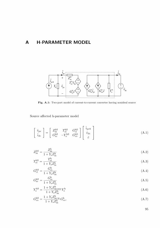
A H-PARAMETER MODEL
pvSi
pvv
h
inZ
h
oi dcˆT v
h
ciˆG c
h
io pvˆG i
h
coˆG c
h
oY dcv
dci
SY
pvi
Fig. A.1: Two-port model of current-to-current converter having nonideal source
Source affected h-parameter model
[
vpv
idc
]
=
[
ZhSin T hS
oi GhSci
GhSio −Y hS
o GhSco
]
ipvS
vdc
c
(A.1)
ZhSin =
Zhin
1 + YsZhin
(A.2)
T hSoi =
T hoi
1 + YsZhin
(A.3)
GhSci =
Ghci
1 + YsZhin
(A.4)
GhSio =
Ghio
1 + YsZhin
(A.5)
Y hSo =
1 + YsZhin-oco
1 + YsZhin
Y ho (A.6)
GhSco =
1 + YsZhin-∞
1 + YsZhin
Ghco, (A.7)
95

Appendix A. H-parameter model
Zhin-oco = Zh
in +Gh
ioThoi
Y ho
(A.8)
Zhin−∞ = Zh
in −Gh
ioGhci
Ghco
. (A.9)
Closed-loop transfer functions under input voltage control
[
vpv
idc
]
=
[
Zhin-c T h
oi-c Ghri
Ghio-c −Y h
o-c Ghro
]
ipv
vdc
vrefdc
(A.10)
Zhin-c =
Zhin-o
1 + Lhin
(A.11)
T hoi-c =
T hoi-o
1 + Lhin
(A.12)
Ghri =
Lhin
1 + Lhin
1
Ghse-in
(A.13)
Ghio-c =
Ghio-o
1 + Lhin
+Lhin
1 + Lhin
Ghio-∞ (A.14)
Y ho-c =
Y ho-o
1 + Lhin
+Lhin
1 + Lhin
Y ho-∞ (A.15)
Ghro =
Lhin
1 + Lhin
Ghco-o
Ghci-o
1
Ghse-in
, (A.16)
where
Lhin = Gh
se-inGcGaGhci-o (A.17)
Ghio-∞ = Gh
io-o −Zhin-oG
hco-o
Ghci-o
(A.18)
Y ho-∞ = Y h
o-o +T hoi-oG
hco-o
Ghci-o
(A.19)
96
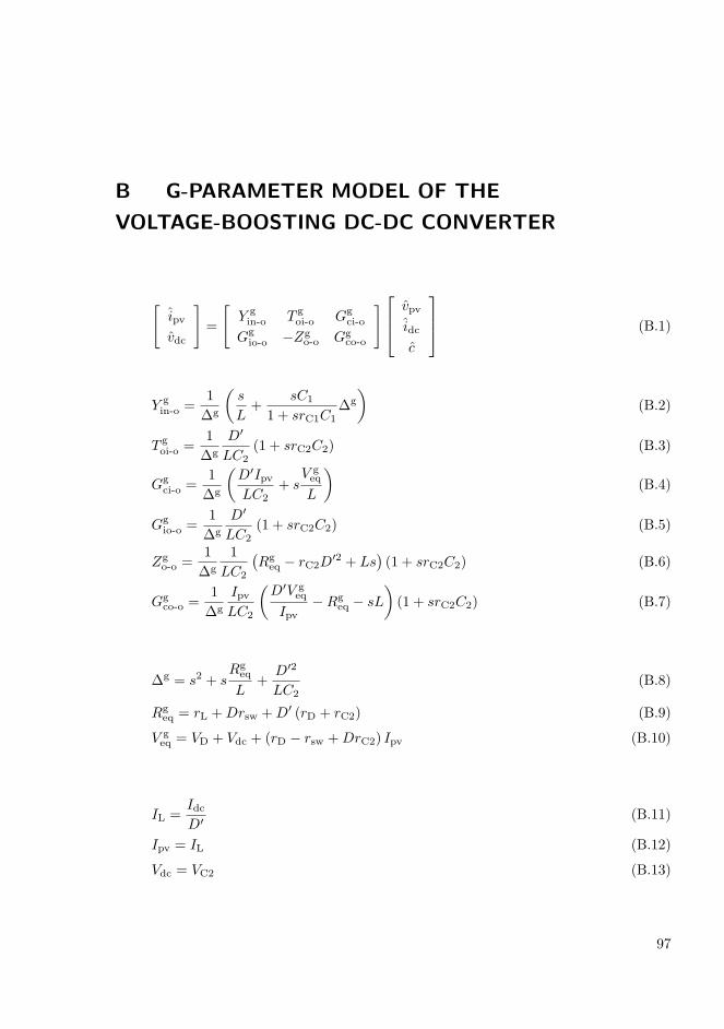
B G-PARAMETER MODEL OF THE
VOLTAGE-BOOSTING DC-DC CONVERTER
[
ipv
vdc
]
=
[
Y gin-o T g
oi-o Ggci-o
Ggio-o −Zg
o-o Ggco-o
]
vpv
idc
c
(B.1)
Y gin-o =
1
∆g
(
s
L+
sC1
1 + srC1C1∆g
)
(B.2)
T goi-o =
1
∆g
D′
LC2(1 + srC2C2) (B.3)
Ggci-o =
1
∆g
(
D′IpvLC2
+ sV geq
L
)
(B.4)
Ggio-o =
1
∆g
D′
LC2(1 + srC2C2) (B.5)
Zgo-o =
1
∆g
1
LC2
(
Rgeq − rC2D
′2 + Ls)
(1 + srC2C2) (B.6)
Ggco-o =
1
∆g
IpvLC2
(
D′V geq
Ipv−Rg
eq − sL
)
(1 + srC2C2) (B.7)
∆g = s2 + sRg
eq
L+
D′2
LC2(B.8)
Rgeq = rL +Drsw +D′ (rD + rC2) (B.9)
V geq = VD + Vdc + (rD − rsw +DrC2) Ipv (B.10)
IL =IdcD′
(B.11)
Ipv = IL (B.12)
Vdc = VC2 (B.13)
97

Appendix B. G-parameter model of the voltage-boosting dc-dc converter
(rC2Idc − VD − Vdc)D′2 + (Vpv − (rD + rC2 − rsw) Ipv + Vpv)D
′
− (rL + rsw) Idc = 0 (B.14)
pvSv
pvvg
inY
g
ciˆG c
g
io pvˆG v
g
coˆG c
g
oZ
dcv
dci
SZpvi
g
oi dcˆT i
Fig. B.1: Two-port model of voltage-to-voltage converter having nonideal source
Source affected g-parameter model
[
ipv
vdc
]
=
[
Y gSin T gS
oi GgSci
GgSio −ZgS
o GgSco
]
vpvS
idc
c
(B.15)
Y gSin =
Y zin
1 + ZsYgin
(B.16)
T gSoi =
T zoi
1 + ZsYgin
(B.17)
GgSci =
Gzci
1 + ZsYgin
(B.18)
GgSio =
Gzio
1 + ZsYgin
(B.19)
ZgSo =
1 + ZsYgin-sco
1 + ZsYgin
Y go (B.20)
GgSco =
1 + ZsYgin-∞
1 + ZsYgin
Ggco, (B.21)
98
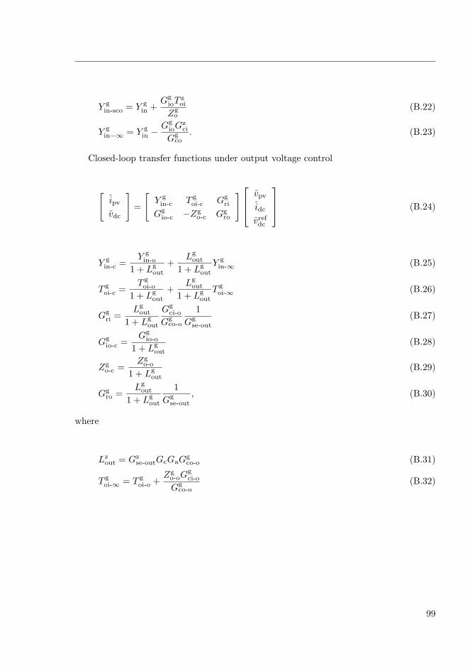
Y gin-sco = Y g
in +Gg
ioTzoi
Zgo
(B.22)
Y gin−∞ = Y g
in − GgioG
zci
Ggco
. (B.23)
Closed-loop transfer functions under output voltage control
[
ipv
vdc
]
=
[
Y gin-c T g
oi-c Ggri
Ggio-c −Zg
o-c Ggro
]
vpv
idc
vrefdc
(B.24)
Y gin-c =
Y gin-o
1 + Lgout
+Lgout
1 + Lgout
Y gin-∞ (B.25)
T goi-c =
T goi-o
1 + Lgout
+Lgout
1 + Lgout
T goi-∞ (B.26)
Ggri =
Lgout
1 + Lgout
Ggci-o
Ggco-o
1
Ggse-out
(B.27)
Ggio-c =
Ggio-o
1 + Lgout
(B.28)
Zgo-c =
Zgo-o
1 + Lgout
(B.29)
Ggro =
Lgout
1 + Lgout
1
Ggse-out
, (B.30)
where
Lzout = Gz
se-outGcGaGgco-o (B.31)
T goi-∞ = T g
oi-o +Zgo-oG
gci-o
Ggco-o
(B.32)
99

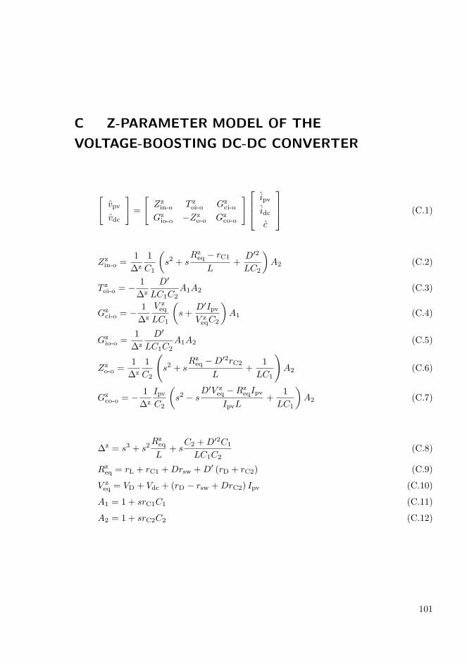
C Z-PARAMETER MODEL OF THE
VOLTAGE-BOOSTING DC-DC CONVERTER
[
vpv
vdc
]
=
[
Zzin-o T z
oi-o Gzci-o
Gzio-o −Zz
o-o Gzco-o
]
ipv
idc
c
(C.1)
Zzin-o =
1
∆z
1
C1
(
s2 + sRz
eq − rC1
L+
D′2
LC2
)
A2 (C.2)
T zoi-o = − 1
∆z
D′
LC1C2A1A2 (C.3)
Gzci-o = − 1
∆z
V zeq
LC1
(
s+D′IpvV zeqC2
)
A1 (C.4)
Gzio-o =
1
∆z
D′
LC1C2A1A2 (C.5)
Zzo-o =
1
∆z
1
C2
(
s2 + sRz
eq −D′2rC2
L+
1
LC1
)
A2 (C.6)
Gzco-o = − 1
∆z
IpvC2
(
s2 − sD′V z
eq −RzeqIpv
IpvL+
1
LC1
)
A2 (C.7)
∆z = s3 + s2Rz
eq
L+ s
C2 +D′2C1
LC1C2(C.8)
Rzeq = rL + rC1 +Drsw +D′ (rD + rC2) (C.9)
V zeq = VD + Vdc + (rD − rsw +DrC2) Ipv (C.10)
A1 = 1 + srC1C1 (C.11)
A2 = 1 + srC2C2 (C.12)
101
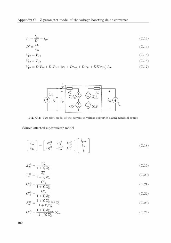
Appendix C. Z-parameter model of the voltage-boosting dc-dc converter
IL =IdcD′
= Ipv (C.13)
D′ =IdcIpv
(C.14)
Vpv = VC1 (C.15)
Vdc = VC2 (C.16)
Vpv = D′Vdc +D′VD + (rL +Drsw +D′rD +DD′rC2) Ipv (C.17)
pvSi
pvv
z
inZ
z
oi dcˆT v
z
ciˆG c
dcv
dci
SY
pvi
z
inZz
io pvˆG i
z
coˆG c
Fig. C.1: Two-port model of the current-to-voltage converter having nonideal source
Source affected z-parameter model
[
vpv
vdc
]
=
[
ZzSin T zS
oi GzSci
GzSio −ZzS
o GzSco
]
ipvS
idc
c
(C.18)
ZzSin =
Zzin
1 + YsZzin
(C.19)
T zSoi =
T zoi
1 + YsZzin
(C.20)
GzSci =
Gzci
1 + YsZzin
(C.21)
GzSio =
Gzio
1 + YsZzin
(C.22)
ZzSo =
1 + YsZzin-sco
1 + YsZzin
Zzo (C.23)
GzSco =
1 + YsZzin-∞
1 + YsZzin
Gzco, (C.24)
102

Zzin-sco = Zz
in +Gz
ioTzoi
Zzo
(C.25)
Zzin−∞ = Zh
in − GzioG
zci
Gzco
. (C.26)
Closed-loop transfer functions under output voltage control
[
vpv
vdc
]
=
[
Zzin-c T z
oi-c Gzri
Gzio-c −Zz
o-c Gzro
]
ipv
idc
vrefdc
(C.27)
Zzin-c =
Zzin-o
1 + Lzout
+Lzout
1 + Lzout
Zzin-∞ (C.28)
T zoi-c =
T zoi-o
1 + Lzout
+Lzout
1 + Lzout
T zoi-∞ (C.29)
Gzri =
Lzout
1 + Lzout
Gzci-o
Gzco-o
1
Gzse-out
(C.30)
Gzio-c =
Gzio-o
1 + Lzout
(C.31)
Zzo-c =
Zzo-o
1 + Lzout
(C.32)
Gzro =
Lzout
1 + Lzout
1
Gzse-out
, (C.33)
where
Lzout = Gz
se-outGcGaGzco-o (C.34)
T zoi-∞ = T z
oi-o +Zzo-oG
zci-o
Gzco-o
(C.35)
103

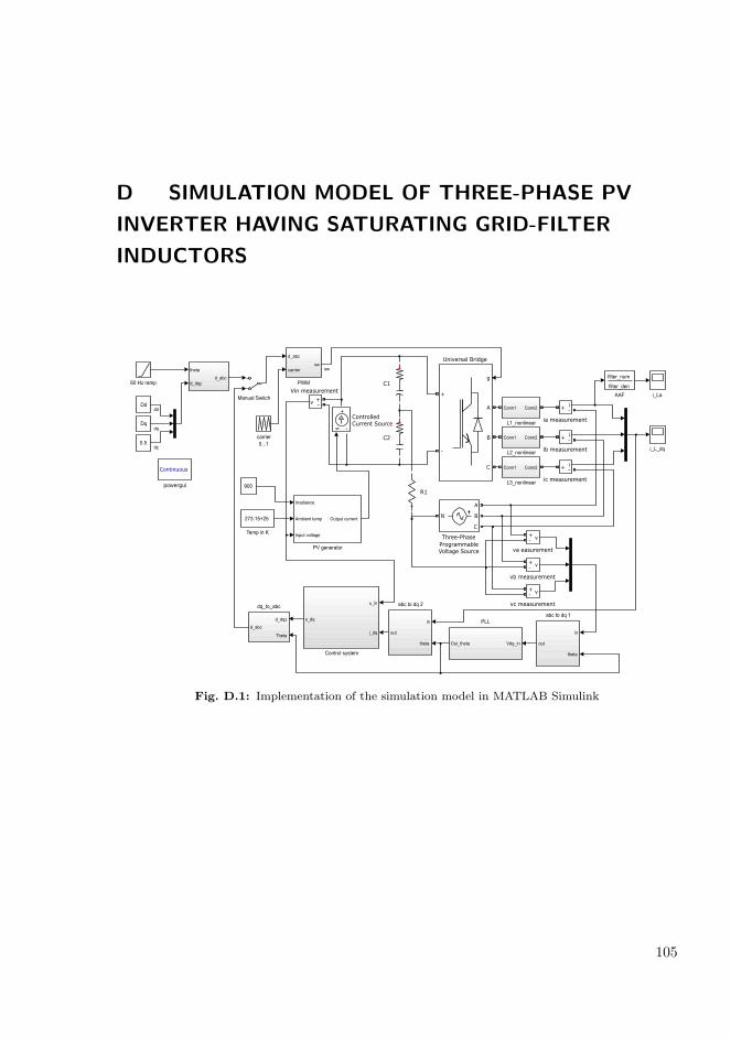
D SIMULATION MODEL OF THREE-PHASE PV
INVERTER HAVING SATURATING GRID-FILTER
INDUCTORS
0.5
Dd
Dq
i_L_dq
theta
d_dqzd_abc
carrier
0...1
+
C1
d_abc
carriersw
PWMg
A
B
C
+
-
Universal Bridge
v+-
va easurement
v +-
Vin measurement
Continuous
powergui
N
A
B
C
Three-Phase
ProgrammableVoltage Source
i+-
ia measurement
i+-
ic measurement
s -+
ControlledCurrent Source
i+ -
ib measurement
60 Hz ramp
u_in
i_dq
s_dq
Control system
filter_num
filter_den
AAF i_LaManual Switch
v+-
vb measurement
v+-
vc measurement
+
R1
+
C2
d_dqz
Theta
d_abc
dq_to_abc
Conn1 Conn2
L1_nonlinear
Conn1 Conn2
L2_nonlinear
Conn1 Conn2
L3_nonlinear
Vdq_inOut_theta
PLL
in
theta
out
abc to dq 1
in
theta
out
abc to dq 2
900
273.15+25
Temp in K
Irradiance
Ambient temp
Input voltage
Output current
PV generator
dz
dq
sw
dd
Fig. D.1: Implementation of the simulation model in MATLAB Simulink
105


E LABORATORY SETUP
PC
Oscilloscope
PV emulator
dspace
Current
L-filter
Inverter hardware
Three-phase
Transformer
voltage supply
amplifiers
Fig. E.1: Laboratory setup for measuring the three-phase PV inverter
107

ISBN 978-952-15-4049-3
ISSN 1459-2045
Tampereen teknillinen yliopisto PL 52733101 Tampere
Tampere University of TechnologyP.O.B. 527FI-33101 Tampere, Finland
Top Related