


Languages
Pages
Legal

Intel® 810E Chipset: 82810E Graphics and Memory Controller Hub (GMCH) Datasheet
September 2000
Order Number: 290676-002
R

Intel® 82810E (GMCH)
R
2 Datasheet
Information in this document is provided in connection with Intel products. No license, express or implied, by estoppel or otherwise, to any intellectual property rights is granted by this document. Except as provided in Intel’s Terms and Conditions of Sale for such products, Intel assumes no liability whatsoever, and Intel disclaims any express or implied warranty, relating to sale and/or use of Intel products including liability or warranties relating to fitness for a particular purpose, merchantability, or infringement of any patent, copyright or other intellectual property right. Intel products are not intended for use in medical, life saving, or life sustaining applications.
Intel may make changes to specifications and product descriptions at any time, without notice.
Designers must not rely on the absence or characteristics of any features or instructions marked "reserved" or "undefined." Intel reserves these for future definition and shall have no responsibility whatsoever for conflicts or incompatibilities arising from future changes to them.
The Intel® 810E chipset may contain design defects or errors known as errata which may cause the product to deviate from published specifications. Current characterized errata are available on request.
Contact your local Intel sales office or your distributor to obtain the latest specifications and before placing your product order.
I2C is a 2-wire communications bus/protocol developed by Philips. SMBus is a subset of the I2C bus/protocol and was developed by Intel. Implementations of the I2C bus/protocol may require licenses from various entities, including Philips Electronics N.V. and North American Philips Corporation.
Alert on LAN is a result of the Intel-IBM Advanced Manageability Alliance and a trademark of IBM
Copies of documents which have an ordering number and are referenced in this document, or other Intel literature, may be obtained from:
Intel Corporation
www.intel.com
or call 1-800-548-4725
*Third-party brands and names are the property of their respective owners.
Copyright © Intel Corporation 2000

Intel® 82810E (GMCH)
R
Datasheet 3
Contents 1. Overview.....................................................................................................................................11
1.1. The Intel® 810E Chipset System ....................................................................................11 1.2. GMCH Overview ............................................................................................................13 1.3. Host Interface.................................................................................................................14 1.4. System Memory Interface ..............................................................................................14 1.5. Display Cache Interface .................................................................................................14 1.6. Hub Interface..................................................................................................................14 1.7. GMCH Graphics Support ...............................................................................................15
1.7.1. Display, Digital Video Out, and LCD/Flat Panel ...........................................15 1.8. System Clocking ............................................................................................................16 1.9. References.....................................................................................................................16
2. Signal Description.......................................................................................................................17 2.1. Host Interface Signals ....................................................................................................18 2.2. System Memory Interface Signals .................................................................................19 2.3. Display Cache Interface Signals ....................................................................................20 2.4. Hub Interface Signals.....................................................................................................20 2.5. Display Interface Signals................................................................................................21 2.6. Digital Video Output Signals/TV-Out Pins......................................................................22 2.7. Power Signals ................................................................................................................23 2.8. Clock Signals .................................................................................................................23 2.9. Miscellaneous Interface Signals.....................................................................................24 2.10. Power-Up/Reset Strap Options......................................................................................24
3. Configuration Registers ..............................................................................................................25 3.1. Register Nomenclature and Access Attributes ..............................................................25 3.2. PCI Configuration Space Access...................................................................................26
3.2.1. PCI Bus Configuration Mechanism..............................................................26 3.2.2. Logical PCI Bus #0 Configuration Mechanism.............................................27 3.2.3. Primary PCI (PCI0) and Downstream Configuration Mechanism ................27 3.2.4. Internal Graphics Device Configuration Mechanism....................................27 3.2.5. GMCH Register Introduction........................................................................27
3.3. I/O Mapped Registers ....................................................................................................28 3.3.1. CONFIG_ADDRESSConfiguration Address Register..............................28 3.3.2. CONFIG_DATAConfiguration Data Register ...........................................29
3.4. Host-Hub Interface Bridge/DRAM Controller Device Registers (Device 0)....................30 3.4.1. VIDVendor Identification Register (Device 0)...........................................31 3.4.2. DIDDevice Identification Register (Device 0) ...........................................31 3.4.3. PCICMDPCI Command Register (Device 0)............................................32 3.4.4. PCISTSPCI Status Register (Device 0) ...................................................33 3.4.5. RIDRevision Identification Register (Device 0) ........................................34 3.4.6. SUBCSub-Class Code Register (Device 0) .............................................34 3.4.7. BCCBase Class Code Register (Device 0) ..............................................34 3.4.8. MLTMaster Latency Timer Register (Device 0) .......................................35 3.4.9. HDRHeader Type Register (Device 0) .....................................................35 3.4.10. SVIDSubsystem Vendor Identification Register (Device 0)......................35 3.4.11. SIDSubsystem Identification Register (Device 0).....................................36

Intel® 82810E (GMCH)
R
4 Datasheet
3.4.12. CAPPTRCapabilities Pointer (Device 0) .................................................. 36 3.4.13. GMCHCFGGMCH Configuration Register (Device 0) ............................. 37 3.4.14. PAMR—Programmable Attributes Register (Device 0)............................... 38 3.4.15. DRPDRAM Row Population Register (Device 0)..................................... 39 3.4.16. DRAMTDRAM Timing Register (Device 0).............................................. 41 3.4.17. FCHCFixed DRAM Hole Control Register (Device 0).............................. 42 3.4.18. SMRAMSystem Management RAM Control Register (Device 0) ........... 43 3.4.19. MISCCMiscellaneous Control Register (Device 0) .................................. 45 3.4.20. MISCC2Miscellaneous Control 2 Register (Device 0) ............................. 46 3.4.21. BUFF_SC—System Memory Buffer Strength Control Register (Device 0). 47
3.5. Graphics Device Registers (Device 1)........................................................................... 49 3.5.1. VIDVendor Identification Register (Device 1) .......................................... 50 3.5.2. DIDDevice Identification Register (Device 1)........................................... 50 3.5.3. PCICMDPCI Command Register (Device 1) ........................................... 51 3.5.4. PCISTSPCI Status Register (Device 1)................................................... 52 3.5.5. RIDRevision Identification Register (Device 1) ........................................ 53 3.5.6. PI-Programming Interface Register (Device 1) ........................................... 53 3.5.7. SUBC1—Sub-Class Code Register (Device 1)........................................... 53 3.5.8. BCC1—Base Class Code Register (Device 1)............................................ 54 3.5.9. CLSCache Line Size Register (Device 1) ................................................ 54 3.5.10. MLTMaster Latency Timer Register (Device 1) ....................................... 54 3.5.11. HDRHeader Type Register (Device 1)..................................................... 55 3.5.12. BISTBuilt In Self Test (BIST) Register (Device 1) ................................... 55 3.5.13. GMADRGraphics Memory Range Address Register (Device 1) ............. 56 3.5.14. MMADRMemory Mapped Range Address Register (Device 1)............... 57 3.5.15. SVIDSubsystem Vendor Identification Register (Device 1) ..................... 57 3.5.16. SIDSubsystem Identification Register (Device 1) .................................... 58 3.5.17. ROMADRVideo BIOS ROM Base Address Registers (Device 1)........... 58 3.5.18. CAPPOINTCapabilities Pointer Register (Device 1)................................ 58 3.5.19. INTRLINEInterrupt Line Register (Device 1) ........................................... 59 3.5.20. INTRPINInterrupt Pin Register (Device 1) ............................................... 59 3.5.21. MINGNTMinimum Grant Register (Device 1) .......................................... 59 3.5.22. MAXLATMaximum Latency Register (Device 1) ..................................... 59 3.5.23. PM_CAPIDPower Management Capabilities ID Register (Device 1) ...... 60 3.5.24. PM_CAPPower Management Capabilities Register (Device 1)............... 60 3.5.25. PM_CS—Power Management Control/Status Register (Device 1)............ 61
3.6. Display Cache Interface................................................................................................. 62 3.6.1. DRT—DRAM Row Type.............................................................................. 62 3.6.2. DRAMCL—DRAM Control Low................................................................... 63 3.6.3. DRAMCH—DRAM Control High.................................................................. 64
3.7. Display Cache Detect and Diagnostic Registers ........................................................... 65 3.7.1. GRXGRX Graphics Controller Index Register ......................................... 65 3.7.2. MSRMiscellaneous Output ...................................................................... 66 3.7.3. GR06Miscellaneous Register .................................................................. 67 3.7.4. GR10Address Mapping............................................................................ 68 3.7.5. GR11Page Selector ................................................................................. 68
4. Functional Description................................................................................................................ 69 4.1. System Address Map .................................................................................................... 69
4.1.1. Memory Address Ranges............................................................................ 70 4.1.1.1. Compatibility Area........................................................................... 71 4.1.1.2. Extended Memory Area .................................................................. 73
Intel® 82810E (GMCH)
R
Datasheet 5
4.1.1.3. System Management Mode (SMM) Memory Range.......................75 4.1.2. Memory Shadowing .....................................................................................76 4.1.3. I/O Address Space.......................................................................................76 4.1.4. GMCH Decode Rules and Cross-Bridge Address Mapping ........................77
4.2. Host Interface.................................................................................................................77 4.2.1. Host Bus Device Support.............................................................................77 4.2.2. Special Cycles..............................................................................................80
4.3. System Memory DRAM Interface...................................................................................81 4.3.1. DRAM Organization and Configuration........................................................81
4.3.1.1. Configuration Mechanism For DIMMs.............................................82 4.3.1.2. DRAM Register Programming.........................................................82
4.3.2. DRAM Address Translation and Decoding ..................................................83 4.3.3. DRAM Array Connectivity ............................................................................85 4.3.4. SDRAMT Register Programming.................................................................85 4.3.5. SDRAM Paging Policy .................................................................................86
4.4. Intel Dynamic Video Memory Technology (D.V.M.T.) ..................................................86 4.5. Display Cache Interface .................................................................................................86
4.5.1. Supported DRAM Types ..............................................................................87 4.5.2. Memory Configurations................................................................................87 4.5.3. Address Translation .....................................................................................88 4.5.4. Display Cache Interface Timing...................................................................88
4.6. Internal Graphics Device................................................................................................89 4.6.1. 3D/2D Instruction Processing ......................................................................89 4.6.2. 3D Engine ....................................................................................................90 4.6.3. Buffers..........................................................................................................90 4.6.4. Setup............................................................................................................91 4.6.5. Texturing ......................................................................................................92 4.6.6. 2D Operation................................................................................................94 4.6.7. Fixed Blitter (BLT) and Stretch Blitter (STRBLT) Engines ...........................94
4.6.7.1. Fixed BLT Engine............................................................................95 4.6.7.2. Arithmetic Stretch BLT Engine ........................................................95
4.6.8. Hardware Motion Compensation .................................................................95 4.6.9. Hardware Cursor..........................................................................................96 4.6.10. Overlay Engine.............................................................................................96 4.6.11. Display .........................................................................................................96 4.6.12. Flat Panel Interface / 1.8V TV-Out Interface................................................99 4.6.13. DDC (Display Data Channel) .....................................................................100
4.7. System Reset for the GMCH .......................................................................................101 4.8. System Clock Description ............................................................................................101 4.9. Power Management .....................................................................................................101
4.9.1. Specifications Supported ...........................................................................101
5. Pinout and Package Information ..............................................................................................103 5.1. 82810E GMCH Pinout..................................................................................................103 5.2. Package Dimensions ...................................................................................................109
6. Testability..................................................................................................................................111 6.1. XOR TREE Testability Algorithm Example ..................................................................112
6.1.1. Test Pattern Consideration for XOR Chain 7.............................................112 6.2. XOR Tree Initialization .................................................................................................113
6.2.1. Chain [1:2, 4:7] Initialization .......................................................................113 6.2.2. Chain 3 Initialization ...................................................................................113
6.3. XOR Chain Pin Assignments .......................................................................................114
Intel® 82810E (GMCH)
R
6 Datasheet
Figures Figure 1. Intel® 810E Chipset System Block Diagram With Intel 82810E GMCH and ICH...... 12 Figure 2. GMCH Block Diagram............................................................................................... 13 Figure 3. System Memory Address Map.................................................................................. 70 Figure 4. Detailed Memory System Address Map.................................................................... 71 Figure 5 GMCH’s Graphics Register Memory Address Space ................................................ 74 Figure 6. DRAM Array Sockets (2 DIMM Sockets) .................................................................. 85 Figure 7. GMCH Display Cache Interface to 4 MB................................................................... 87 Figure 8. 3D/2D Pipeline Preprocessor.................................................................................... 89 Figure 9. Data Flow for the 3D Pipeline ................................................................................... 91 Figure 10. GMCH Pinout (Top View—Left Side).................................................................... 104 Figure 11. GMCH Pinout (Top View—Right Side) ................................................................. 105 Figure 12. GMCH Package Dimensions (421 BGA) – Top and Side Views .......................... 109 Figure 13. GMCH Package Dimensions (421 BGA) – Bottom View...................................... 110 Figure 14. XOR Tree Implementation .................................................................................... 111
Tables Table 1. Power Up Options ......................................................................................................24 Table 2. Host Frequency Strappings........................................................................................ 24 Table 3. GMCH PCI Configuration Space (Device 0) .............................................................. 30 Table 4. Programming DRAM Row Population Register Fields............................................... 40 Table 5. GMCH Configuration Space (Device 1) ..................................................................... 49 Table 6 Memory Mapped Registers ......................................................................................... 62 Table 7. Memory Segments and their Attributes...................................................................... 72 Table 8. Summay of Transactions Supported By GMCH......................................................... 78 Table 9. Host Responses Supported by the GMCH ................................................................ 79 Table 10. Special Cycles.......................................................................................................... 80 Table 11. Sample Of Possible Mix And Match Options For 4 Row/2 DIMM Configurations.... 82 Table 12. Data Bytes on DIMM Used for Programming DRAM Registers............................... 83 Table 13. GMCH DRAM Address Mux Function...................................................................... 84 Table 14. Programmable SDRAM Timing Parameters ............................................................ 85 Table 15. Memory Size for Each Configuration........................................................................ 87 Table 16. Partial List of Display Modes Supported .................................................................. 97 Table 17. Partial List of Flat Panel Modes Supported.............................................................. 99 Table 18. Partial List of TV-Out Modes Supported ................................................................ 100 Table 19. Alphabetical Pin Assignment.................................................................................. 106 Table 20. GMCH Package Dimensions (421 BGA) ............................................................... 110 Table 21. XOR Test Pattern Example.................................................................................... 112 Table 22. XOR Chain 1 ..........................................................................................................114 Table 23. XOR Chain 2 ..........................................................................................................114 Table 24. XOR Chain 3 ..........................................................................................................115 Table 25. XOR Chain 4 ..........................................................................................................116 Table 26. XOR Chain 5 ..........................................................................................................117 Table 27. XOR Chain 6 ..........................................................................................................118 Table 28. XOR Chain 7 ..........................................................................................................119

Intel® 82810E (GMCH)
R
Datasheet 7
Revision History
Rev. Description Date
-001 Initial Release September 1999
-002 • Added Table 17, “Overlay Modes Supported”
• Added Section 4.9.2, “Resume From S3”
• Updated BUFF_SC Register description (see Section 3.4.21, “BUFF_SC—System Memory Buffer Strength Control Register (Device 0)”)
• Editorial changes throughout for clarity
September 2000
Intel® 82810E (GMCH)
R
8 Datasheet
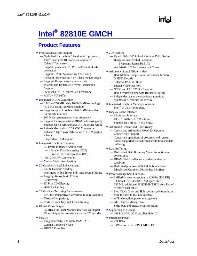
Intel® 82810E GMCH Product Features
! Processor/Host Bus Support Optimized for the Intel Pentium II processor,
Intel Pentium III processor, and Intel CeleronTM processor
Supports processor 370-Pin Socket and SC242 connectors
Supports 32-Bit System Bus Addressing 4 deep in-order queue; 4 or 1 deep request queue Supports Uni-processor systems only In-order and Dynamic Deferred Transaction
Support 66/100/133 MHz System Bus Frequency AGTL+ I/O Buffer ! Integrated DRAM Controller
8 MB to 256 MB using 16Mb/64Mb technology (512 MB using 128Mb technology)
Supports up to 2 double sided DIMM modules 64-bit data interface 100 MHz system memory bus frequency Support for Asymmetrical DRAM addressing only Support for x8, x16 and x32 DRAM device width Refresh Mechanism: CBR ONLY supported Enhanced Open page Arbitration SDRAM paging
scheme Suspend to RAM support ! Integrated Graphics Controller
3D Hyper Pipelined Architecture -Parallel Data Processing (PDP) -Precise Pixel Interpolation (PPI)
Full 2D H/W Acceleration Motion Video Acceleration ! 3D Graphics Visual Enhancements
Flat & Gouraud Shading Mip Maps with Bilinear and Anisotropic Filtering Fogging Atmospheric Effects Z Buffering 3D Pipe 2D Clipping Backface Culling ! 3D Graphics Texturing Enhancements
Per Pixel Perspective Correction Texture Mapping Texture Compositing Texture Color Keying/Chroma Keying ! Digital Video Output
85 MHz Flat Panel Monitor Interface Or Digital Video Output for use with a external TV encoder
! Display Integrated 24-bit 230 MHz RAMDAC Gamma Corrected Video DDC2B Compliant
! 2D Graphics Up to 1600x1200 in 8-bit Color at 75 Hz Refresh Hardware Accelerated Functions
3 Operand Raster BitBLTs 64x64x3 Color Transparent Cursor
! Arithmetic Stretch Blitter Video H/W Motion Compensation Assistance for S/W
MPEG2 Decode Software DVD at 30 fps Digital Video Out Port NTSC and PAL TV Out Support H/W Overlay Engine with Bilinear Filtering Independent gamma correction, saturation,
brightness & contrast for overlay ! Integrated Graphics Memory Controller
Intel D.V.M. Technology ! Display Cache Interface
32-bit data interface 100/133 MHz SDRAM interface Support for 1Mx16, (4 MB Only) ! Arbitration Scheme and Concurrency
Centralized Arbitration Model for Optimum Concurrency Support
Concurrent operations of processor and system busses supported via dedicated arbitration and data buffering
! Data Buffering Distributed Data Buffering Model for optimum
concurrency DRAM Write Buffer with read-around-write
capability Dedicated processor -DRAM, hub interface-
DRAM and Graphics-DRAM Read Buffers ! Power Management Functions
SMRAM space remapping to A0000h (128 KB) Optional Extended SMRAM space above
256 MB, additional 512K/1MB TSEG from Top of Memory, cacheable
Stop Clock Grant and Halt special cycle translation from the host to the hub interface
ACPI Compliant power management APIC Buffer Management SMI, SCI, and SERR error indication ! Supporting I/O Bridge
241 Pin BGA I/O Controller Hub ICH ! Packaging/Power
421 BGA 1.8V core with 3.3V CMOS I/O

Intel® 82810E (GMCH)
R
Datasheet 9
GMCH Simplified Block Diagram
gmch_blk.vsd
HA[31:3]#HD[63:0]#
ADS#BNR#BPRI#
DBSY#DEFER#
DRDY#HIT#
HITM#HLOCK#
HREQ[4:0]#HTRDY#RS[2:0]#
CPURST#
System BusInterface
SMAA[11:0]SMAB[7:4]#
SBS[1:0]SMD[63:0]SDQM[7:0]SCS[3:0]#
SRAS#SCAS#SWE#
SCKE[1:0]
SystemMemoryInterface
DisplayCache
Interface82810E
LCS#LDQM[3:0]#
LSRAS#LSCAS#
LMA[11:0]LWE#
LMD[31:0]
DisplayInterface
DigitalTVOut
HubInterface
HUBREFHL[10:0]HLSTRBHLSTRB#HCOMP
VSYNCHSYNCIREFREDGREENBLUEDDCSCLDDCSDA
LTVCLLTVDATVCLKIN/INT#CLKOUT[1:0]BLANK#LTVDATA[11:0]TVSYNCTVHSYNC
ClockSignals
HCLKSCLKLTCLKLOCLKLRCLKDCLKREFHLCLK
GLRREFAGTLREFBRESET#
Misc.InterfaceSignals
.

Intel® 82810E (GMCH)
R
10 Datasheet
This page is intentionally left blank.
Intel® 82810E (GMCH)
R
Datasheet 11
1. Overview The Intel® 810E chipset is a high-integration chipset designed for the basic graphics/multimedia PC platform. The chipset consists of a Graphics and Memory Controller Hub (GMCH) Host Bridge and an I/O Controller Hub (ICH) Bridge for the I/O subsystem. The GMCH integrates a system memory DRAM controller that supports a 64-bit 100 MHz DRAM array. The DRAM controller is optimized for maximum efficiency.
The 82810E integrates a Display Cache DRAM controller that supports a 4 MB, 32-bit 100/133 MHz DRAM array for enhanced 2D and 3D performance.
Note: In this document the term “GMCH” refers to the 82810E, unless otherwise specified.
The Intel® 810E chipset may contain design defects or errors known as errata which may cause the product to deviate from published specifications. Current characterized errata are available on request.
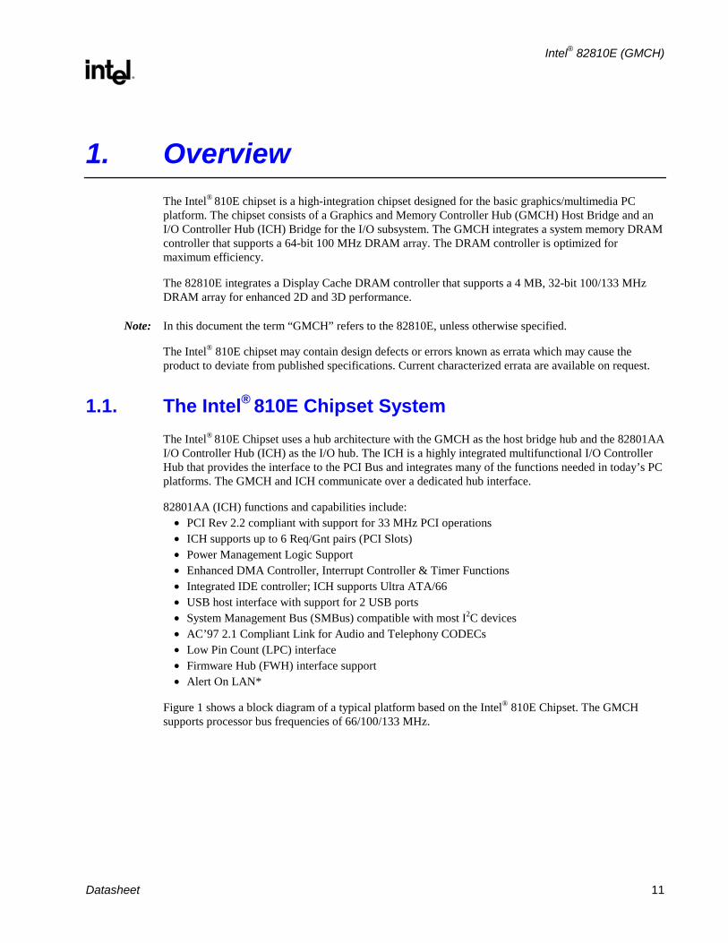
1.1. The Intel® 810E Chipset System The Intel® 810E Chipset uses a hub architecture with the GMCH as the host bridge hub and the 82801AA I/O Controller Hub (ICH) as the I/O hub. The ICH is a highly integrated multifunctional I/O Controller Hub that provides the interface to the PCI Bus and integrates many of the functions needed in today’s PC platforms. The GMCH and ICH communicate over a dedicated hub interface.
82801AA (ICH) functions and capabilities include: • PCI Rev 2.2 compliant with support for 33 MHz PCI operations • ICH supports up to 6 Req/Gnt pairs (PCI Slots) • Power Management Logic Support • Enhanced DMA Controller, Interrupt Controller & Timer Functions • Integrated IDE controller; ICH supports Ultra ATA/66 • USB host interface with support for 2 USB ports • System Management Bus (SMBus) compatible with most I2C devices • AC’97 2.1 Compliant Link for Audio and Telephony CODECs • Low Pin Count (LPC) interface • Firmware Hub (FWH) interface support • Alert On LAN*
Figure 1 shows a block diagram of a typical platform based on the Intel® 810E Chipset. The GMCH supports processor bus frequencies of 66/100/133 MHz.

Intel® 82810E (GMCH)
R
12 Datasheet
Figure 1. Intel® 810E Chipset System Block Diagram With Intel 82810E GMCH and ICH
System Bus (66/100/133 MHz)
SystemMemory
PCI Bus
PCI Slots(ICH=6 Req/Gnt pairs)
sysblk2.vsd
ISAOption
2 IDE PortsUltra ATA/66
2 USBPorts
USB
USB
Intel® 82810E (GMCH)
- Memory Controller- Graphcs Controller - 3D Engine - 2D Engine - Video Engine
TV
Display
Encoder
(4 MB SDRAM,100/133 MHz Only)
Display Cache
64 Bit /100 MHz Only
ICH(I/O Controller Hub)
SuperI/O
AC'97
FWH(Firmware Hub)
Intel® 810E ChipsetDigital Video Out
Audio Codec
Modem Codec
LANOption
Intel® Pentium ® III Processor,Intel® Pentium ® II Processor,Intel® Celeron™ Processor
Intel® 82810E (GMCH)
R
Datasheet 13
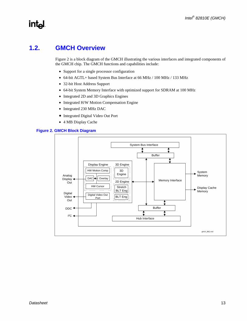
1.2. GMCH Overview Figure 2 is a block diagram of the GMCH illustrating the various interfaces and integrated components of the GMCH chip. The GMCH functions and capabilities include:
• Support for a single processor configuration • 64-bit AGTL+ based System Bus Interface at 66 MHz / 100 MHz / 133 MHz • 32-bit Host Address Support • 64-bit System Memory Interface with optimized support for SDRAM at 100 MHz • Integrated 2D and 3D Graphics Engines • Integrated H/W Motion Compensation Engine • Integrated 230 MHz DAC
• Integrated Digital Video Out Port • 4 MB Display Cache
Figure 2. GMCH Block Diagram
System Bus Interface
Buffer
Memory Interface
Buffer
Hub Interface
SystemMemory
Display CacheMemory
HW Motion Comp
Display Engine 3D Engine
3DEngine
DAC Overlay
HW Cursor
Digital Video OutPort
2D Engine
StretchBLT Eng
BLT Eng
AnalogDisplay
Out
DigitalVideo
Out
DDC
I2C
gmch_blk2.vsd
Intel® 82810E (GMCH)
R
14 Datasheet
1.3. Host Interface The host interface of the GMCH is optimized to support the Intel Pentium® III processor, Intel Pentium® II processor, and Intel CeleronTM processor. The GMCH implements the host address, control, and data bus interfaces within a single device. The GMCH supports a 4-deep in-order queue (i.e., supports pipelining of up to 4 outstanding transaction requests on the host bus) . Host bus addresses are decoded by the GMCH for accesses to system memory, PCI memory and PCI I/O (via hub interface), PCI configuration space and Graphics memory. The GMCH takes advantage of the pipelined addressing capability of the processor to improve the overall system performance.
The GMCH supports the 370-pin socket and SC242 processor connectors.
• 370-pin socket (PGA370). The zero insertion force (ZIF) socket that a processor in the PPGA package will use to interface with a system board.
• SC242—242-contact slot connector. A processor in a Single-Edge Processor Package (SEPP) or Single-Edge Contact Cartidge (SECC and SECC2) use this connector to interface with a system board.
1.4. System Memory Interface The GMCH integrates a system memory DRAM controller that supports a 64-bit 100 MHz DRAM array. The DRAM type supported is industry standard Synchronous DRAM (SDRAM). The DRAM controller interface is fully configurable through a set of control registers. Complete descriptions of these registers are given in the Chapter 3, “Configuration Registers”.
The GMCH supports industry standard 64-bit wide DIMM modules with SDRAM devices. The twelve multiplexed address lines, SMAA[11:0], along with the two bank select lines, SBS[1:0], allow the GMCH to support 2M, 4M, 8M, and 16M x64 DIMMs. Only asymmetric addressing is supported. The GMCH has four SCS# lines, enabling the support of up to four 64-bit rows of DRAM. The GMCH targets SDRAM with CL2 and CL3 and supports both single and double-sided DIMMs. Additionally, the GMCH also provides a seven deep refresh queue. The GMCH can be configured to keep multiple pages open within the memory array, pages can be kept open in any one row of memory.
SCKE[1:0] is used in configurations requiring powerdown mode for the SDRAM.
1.5. Display Cache Interface The 82810E GMCH supports a Display Cache DRAM controller with a 32-bit 100/133 MHz DRAM array. The DRAM type supported is industry standard Synchronous DRAM (SDRAM) like that of the system memory. The local memory DRAM controller interface is fully configurable through a set of control registers. Complete descriptions of these registers are given in Chapter 3, “Configuration Registers”.
1.6. Hub Interface The hub interface is a private interconnect between the GMCH and the ICH.

Intel® 82810E (GMCH)
R
Datasheet 15
1.7. GMCH Graphics Support The Graphics and Memory Controller Hub (GMCH) includes a highly integrated graphics accelerator. Its architecture consists of dedicated multi-media engines executing in parallel to deliver high performance 3D, 2D and motion compensation video capabilities. The 3D and 2D engines are managed by a 3D/2D pipeline preprocessor allowing a sustained flow of graphics data to be rendered and displayed. The deeply pipelined 3D accelerator engine provides 3D graphics quality and performance via per-pixel 3D rendering and parallel data paths that allow each pipeline stage to simultaneously operate on different primitives or portions of the same primitive. The GMCH graphics accelerator engine supports perspective-correct texture mapping, bilinear and anisotropic Mip-Mapping, Gouraud shading, alpha-blending, fogging and Z-buffering. A rich set of 3D instructions permit these features to be independently enabled or disabled.
For the 82810E, a Display Cache (DC) can be used for Z-buffers (Textures and display buffer are located in system memory). If the display cache is not used, the Z-buffer is located in system memory.
The GMCH integrated graphics accelerator’s 2D capabilities include BLT and arithmetic STRBLT engines, a hardware cursor and an extensive set of 2D registers and instructions. The high performance 64-bit BitBLT engine provides hardware acceleration for many common Windows operations.
In addition to its 2D/3D capabilities, the GMCH integrated graphics accelerator also supports full MPEG-2 motion compensation for software-assisted DVD video playback, a VESA DDC2B compliant display interface and a digital video out port that may support (via an external video encoder) NTSC and PAL broadcast standards.
1.7.1. Display, Digital Video Out, and LCD/Flat Panel
The GMCH provides interfaces to a standard progressive scan monitor, TV-Out device, and LCD/Flat Panel transmitter.
• The GMCH directly drives a standard progressive scan monitor up to a resolution of 1600x1200.
• The GMCH provides a Digital Video Out interface to connect an external device to drive an autodetection of 1024x768 non-scalar DDP digital Flat Panel with appropriate EDID 1.x data. The interface has 1.8V signaling to allow it to operate at higher frequencies. This interface can also connect to a 1.8V TV-Out encoder.

Intel® 82810E (GMCH)
R
16 Datasheet
1.8. System Clocking The GMCH has a new type of clocking architecture. It has integrated SDRAM buffers that always run at 100 MHz, regardless of system bus frequency. The system bus frequency is selectable between 66 MHz, 100 MHz, or 133 MHz. The GMCH uses a copy of the USB clock as the DOT Clock input for the graphics pixel clock PLL.
1.9. References • Intel 810E Chipset Design Guide. Contact your field sales representative.
• PC ’99: Contact www.microsoft.com/hwdev
• AGTL+ I/O Specification: Contained in the Intel® Pentium II Processor Databook
• PCI Local bus Specification 2.2: Contact www.pcisig.com
• Intel® 82801AA (ICH) I/O Controller Hub Datasheet
Intel® 82810E (GMCH)
R
Datasheet 17
2. Signal Description This section provides a detailed description of the GMCH signals. The signals are arranged in functional groups according to their associated interface. The states of all of the signals during reset are provided in the System Reset section.
The “#” symbol at the end of a signal name indicates that the active, or asserted state occurs when the signal is at a low voltage level. When “#” is not present after the signal name the signal is asserted when at the high voltage level.
The following notations are used to describe the signal type:
I Input pin
O Output pin
I/OD Input / Open Drain Output pin. This pin requires a pullup to the VCC of the processor core
I/O Bi-directional Input/Output pin
The signal description also includes the type of buffer used for the particular signal:
AGTL+ Open Drain AGTL+ interface signal. Refer to the AGTL+ I/O Specification for complete details
CMOS The CMOS buffers are Low Voltage TTL compatible signals. These are 3.3V only.
LVTTL Low Voltage TTL compatible signals. There are 3.3V only.
1.8V 1.8V signals for the digital video interface
Analog Analog CRT Signals
Note that the processor address and data bus signals (Host Interface) are logically inverted signals (i.e., the actual values are inverted of what appears on the processor bus). This must be taken into account and the addresses and data bus signals must be inverted inside the GMCH. All processor control signals follow normal convention. A 0 indicates an active level (low voltage) if the signal is followed by # symbol and a 1 indicates an active level (high voltage) if the signal has no # suffix.
Intel® 82810E (GMCH)
R
18 Datasheet
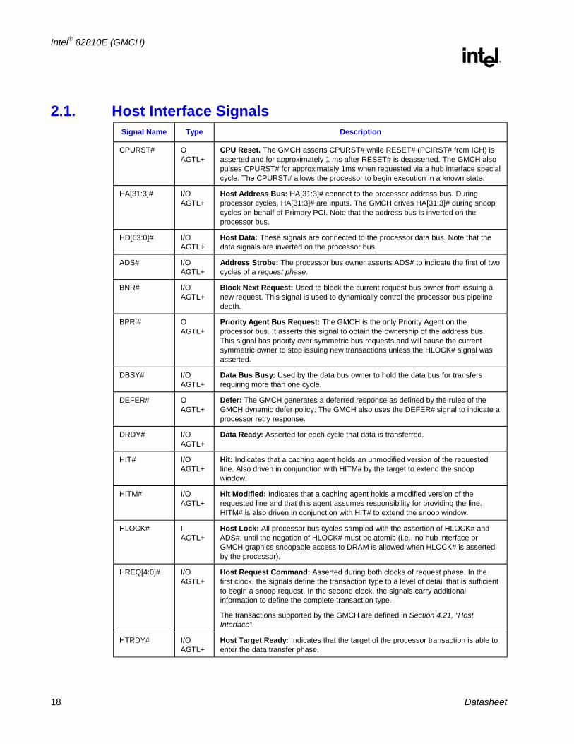
2.1. Host Interface Signals Signal Name Type Description
CPURST# O AGTL+
CPU Reset. The GMCH asserts CPURST# while RESET# (PCIRST# from ICH) is asserted and for approximately 1 ms after RESET# is deasserted. The GMCH also pulses CPURST# for approximately 1ms when requested via a hub interface special cycle. The CPURST# allows the processor to begin execution in a known state.
HA[31:3]# I/O AGTL+
Host Address Bus: HA[31:3]# connect to the processor address bus. During processor cycles, HA[31:3]# are inputs. The GMCH drives HA[31:3]# during snoop cycles on behalf of Primary PCI. Note that the address bus is inverted on the processor bus.
HD[63:0]# I/O AGTL+
Host Data: These signals are connected to the processor data bus. Note that the data signals are inverted on the processor bus.
ADS# I/O AGTL+
Address Strobe: The processor bus owner asserts ADS# to indicate the first of two cycles of a request phase.
BNR# I/O AGTL+
Block Next Request: Used to block the current request bus owner from issuing a new request. This signal is used to dynamically control the processor bus pipeline depth.
BPRI# O AGTL+
Priority Agent Bus Request: The GMCH is the only Priority Agent on the processor bus. It asserts this signal to obtain the ownership of the address bus. This signal has priority over symmetric bus requests and will cause the current symmetric owner to stop issuing new transactions unless the HLOCK# signal was asserted.
DBSY# I/O AGTL+
Data Bus Busy: Used by the data bus owner to hold the data bus for transfers requiring more than one cycle.
DEFER# O AGTL+
Defer: The GMCH generates a deferred response as defined by the rules of the GMCH dynamic defer policy. The GMCH also uses the DEFER# signal to indicate a processor retry response.
DRDY# I/O AGTL+
Data Ready: Asserted for each cycle that data is transferred.
HIT# I/O AGTL+
Hit: Indicates that a caching agent holds an unmodified version of the requested line. Also driven in conjunction with HITM# by the target to extend the snoop window.
HITM# I/O AGTL+
Hit Modified: Indicates that a caching agent holds a modified version of the requested line and that this agent assumes responsibility for providing the line. HITM# is also driven in conjunction with HIT# to extend the snoop window.
HLOCK# I AGTL+
Host Lock: All processor bus cycles sampled with the assertion of HLOCK# and ADS#, until the negation of HLOCK# must be atomic (i.e., no hub interface or GMCH graphics snoopable access to DRAM is allowed when HLOCK# is asserted by the processor).
HREQ[4:0]# I/O AGTL+
Host Request Command: Asserted during both clocks of request phase. In the first clock, the signals define the transaction type to a level of detail that is sufficient to begin a snoop request. In the second clock, the signals carry additional information to define the complete transaction type.
The transactions supported by the GMCH are defined in Section 4.21, “Host Interface”.
HTRDY# I/O AGTL+
Host Target Ready: Indicates that the target of the processor transaction is able to enter the data transfer phase.
Intel® 82810E (GMCH)
R
Datasheet 19
Signal Name Type Description
RS[2:0]# I/O AGTL+
Response Signals: Indicates type of response as shown below:
RS[2:0] Response type 000 Idle state 001 Retry response 010 Deferred response 011 Reserved (not driven by the GMCH) 100 Hard Failure (not driven by the GMCH) 101 No data response 110 Implicit Writeback 111 Normal data response
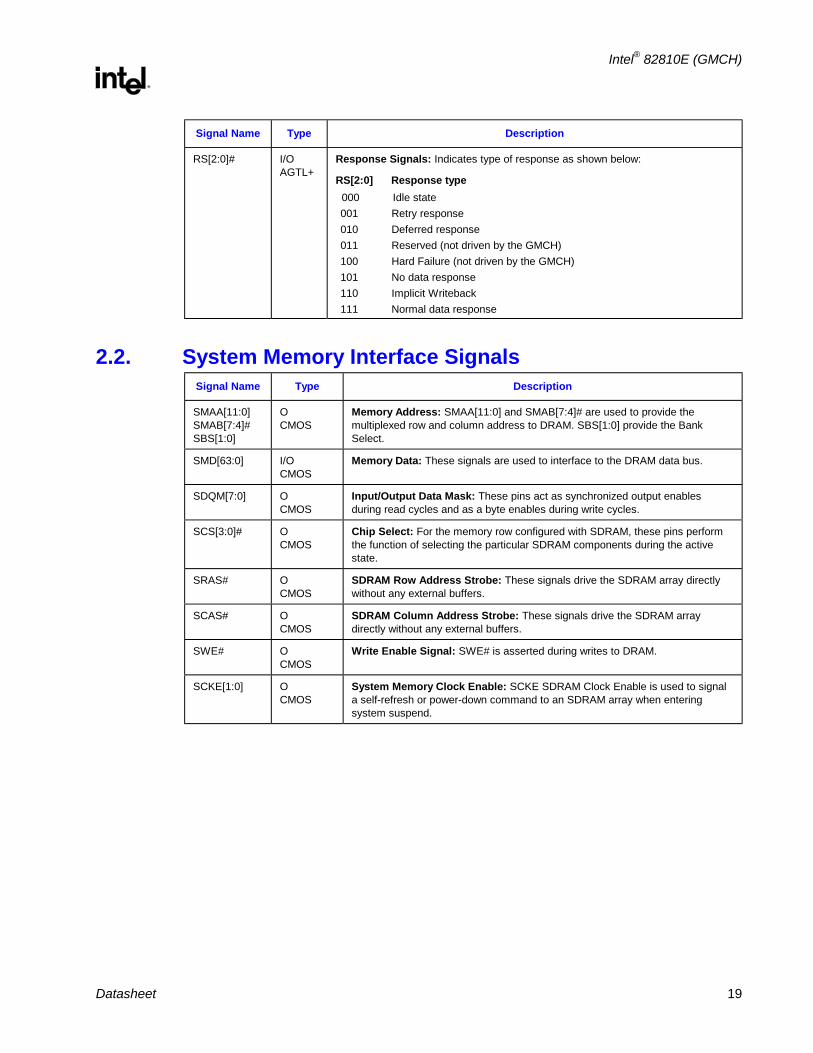
2.2. System Memory Interface Signals Signal Name Type Description
SMAA[11:0] SMAB[7:4]# SBS[1:0]
O CMOS
Memory Address: SMAA[11:0] and SMAB[7:4]# are used to provide the multiplexed row and column address to DRAM. SBS[1:0] provide the Bank Select.
SMD[63:0] I/O CMOS
Memory Data: These signals are used to interface to the DRAM data bus.
SDQM[7:0] O CMOS
Input/Output Data Mask: These pins act as synchronized output enables during read cycles and as a byte enables during write cycles.
SCS[3:0]# O CMOS
Chip Select: For the memory row configured with SDRAM, these pins perform the function of selecting the particular SDRAM components during the active state.
SRAS# O CMOS
SDRAM Row Address Strobe: These signals drive the SDRAM array directly without any external buffers.
SCAS# O CMOS
SDRAM Column Address Strobe: These signals drive the SDRAM array directly without any external buffers.
SWE# O CMOS
Write Enable Signal: SWE# is asserted during writes to DRAM.
SCKE[1:0] O CMOS
System Memory Clock Enable: SCKE SDRAM Clock Enable is used to signal a self-refresh or power-down command to an SDRAM array when entering system suspend.
Intel® 82810E (GMCH)
R
20 Datasheet
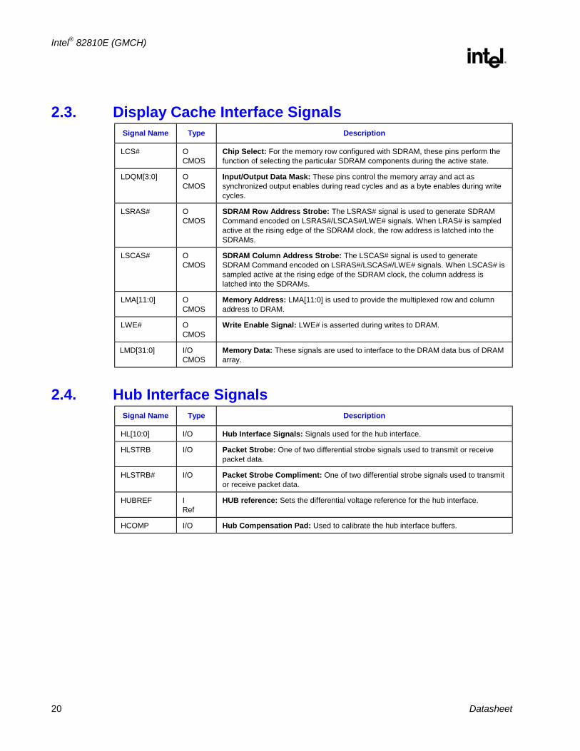
2.3. Display Cache Interface Signals Signal Name Type Description
LCS# O CMOS
Chip Select: For the memory row configured with SDRAM, these pins perform the function of selecting the particular SDRAM components during the active state.
LDQM[3:0] O CMOS
Input/Output Data Mask: These pins control the memory array and act as synchronized output enables during read cycles and as a byte enables during write cycles.
LSRAS# O CMOS
SDRAM Row Address Strobe: The LSRAS# signal is used to generate SDRAM Command encoded on LSRAS#/LSCAS#/LWE# signals. When LRAS# is sampled active at the rising edge of the SDRAM clock, the row address is latched into the SDRAMs.
LSCAS# O CMOS
SDRAM Column Address Strobe: The LSCAS# signal is used to generate SDRAM Command encoded on LSRAS#/LSCAS#/LWE# signals. When LSCAS# is sampled active at the rising edge of the SDRAM clock, the column address is latched into the SDRAMs.
LMA[11:0] O CMOS
Memory Address: LMA[11:0] is used to provide the multiplexed row and column address to DRAM.
LWE# O CMOS
Write Enable Signal: LWE# is asserted during writes to DRAM.
LMD[31:0] I/O CMOS
Memory Data: These signals are used to interface to the DRAM data bus of DRAM array.
2.4. Hub Interface Signals Signal Name Type Description
HL[10:0] I/O Hub Interface Signals: Signals used for the hub interface.
HLSTRB I/O Packet Strobe: One of two differential strobe signals used to transmit or receive packet data.
HLSTRB# I/O Packet Strobe Compliment: One of two differential strobe signals used to transmit or receive packet data.
HUBREF I Ref
HUB reference: Sets the differential voltage reference for the hub interface.
HCOMP I/O Hub Compensation Pad: Used to calibrate the hub interface buffers.

Intel® 82810E (GMCH)
R
Datasheet 21
2.5. Display Interface Signals Signal Name Type Description
VSYNC O 3.3V
CRT Vertical Synchronization: This signal is used as the vertical sync (polarity is programmable) or “ Vsync Interval”.
HSYNC O 3.3V
CRT Horizontal Synchronization: This signal is used as the horizontal sync (polarity is programmable) or “ Hsync Interval”.
IWASTE I Ref
Waste Reference: This signal must be tied to ground.
IREF I Ref
Set pointer resistor for the internal color palette DAC: A 174 ohm 1% resistor is recommended
RED O Analog
CRT Analog video output from the internal color palette DAC: The DAC is designed for a 37.5 ohm equivalent load on each pin (e.g. 75 ohm resistor on the board, in parallel with the 75 ohm CRT load)
GREEN O Analog
CRT Analog video output from the internal color palette DAC: The DAC is designed for a 37.5 ohm equivalent load on each pin (e.g., 75 ohm resistor on the board, in parallel with the 75 ohm CRT load)
BLUE O Analog
CRT Analog video output from the internal color palette DAC: The DAC is designed for a 37.5 ohm equivalent load on each pin (e.g., 75 ohm resistor on the board, in parallel with the 75 ohm CRT load)
DDCSCL I/OD CMOS
CRT Monitor DDC Interface Clock: (Also referred to as VESATM “Display Data Channel”, also referred to as the “Monitor Plug-n-Play” interface.) For DDC1, DDCSCL and DDCSDA provides a unidirectional channel for Extended Display ID. For DDC2, DDCSCL and DDCSDA it can be used to establish a bi-directional channel based on I2C protocol. The host can request Extended Display ID or Video Display Interface information over the DDC2 channel.
DDCSDA I/OD CMOS
CRT Monitor DDC Interface Data:
Intel® 82810E (GMCH)
R
22 Datasheet
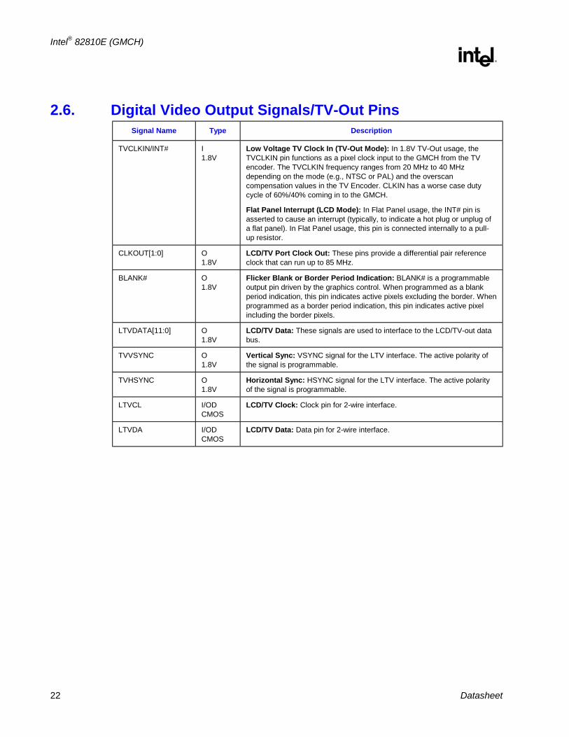
2.6. Digital Video Output Signals/TV-Out Pins Signal Name Type Description
TVCLKIN/INT# I 1.8V
Low Voltage TV Clock In (TV-Out Mode): In 1.8V TV-Out usage, the TVCLKIN pin functions as a pixel clock input to the GMCH from the TV encoder. The TVCLKIN frequency ranges from 20 MHz to 40 MHz depending on the mode (e.g., NTSC or PAL) and the overscan compensation values in the TV Encoder. CLKIN has a worse case duty cycle of 60%/40% coming in to the GMCH.
Flat Panel Interrupt (LCD Mode): In Flat Panel usage, the INT# pin is asserted to cause an interrupt (typically, to indicate a hot plug or unplug of a flat panel). In Flat Panel usage, this pin is connected internally to a pull-up resistor.
CLKOUT[1:0] O 1.8V
LCD/TV Port Clock Out: These pins provide a differential pair reference clock that can run up to 85 MHz.
BLANK# O 1.8V
Flicker Blank or Border Period Indication: BLANK# is a programmable output pin driven by the graphics control. When programmed as a blank period indication, this pin indicates active pixels excluding the border. When programmed as a border period indication, this pin indicates active pixel including the border pixels.
LTVDATA[11:0] O 1.8V
LCD/TV Data: These signals are used to interface to the LCD/TV-out data bus.
TVVSYNC O 1.8V
Vertical Sync: VSYNC signal for the LTV interface. The active polarity of the signal is programmable.
TVHSYNC O 1.8V
Horizontal Sync: HSYNC signal for the LTV interface. The active polarity of the signal is programmable.
LTVCL I/OD CMOS
LCD/TV Clock: Clock pin for 2-wire interface.
LTVDA I/OD CMOS
LCD/TV Data: Data pin for 2-wire interface.
Intel® 82810E (GMCH)
R
Datasheet 23
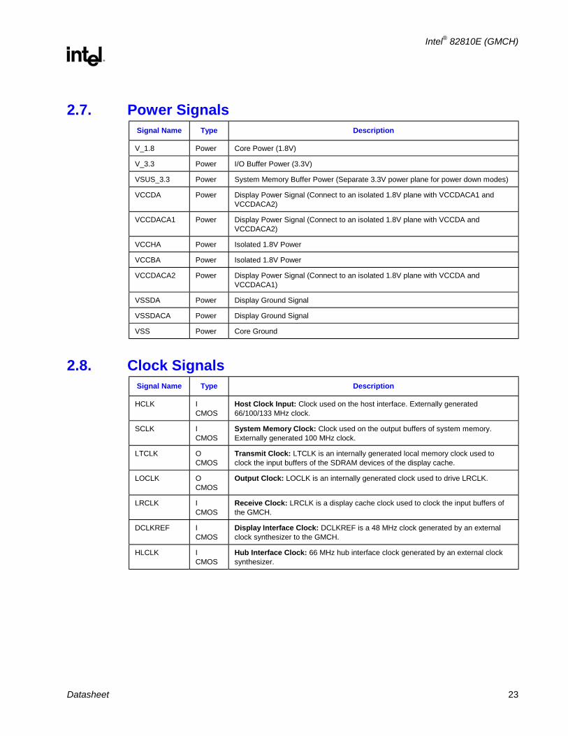
2.7. Power Signals Signal Name Type Description
V_1.8 Power Core Power (1.8V)
V_3.3 Power I/O Buffer Power (3.3V)
VSUS_3.3 Power System Memory Buffer Power (Separate 3.3V power plane for power down modes)
VCCDA Power Display Power Signal (Connect to an isolated 1.8V plane with VCCDACA1 and VCCDACA2)
VCCDACA1 Power Display Power Signal (Connect to an isolated 1.8V plane with VCCDA and VCCDACA2)
VCCHA Power Isolated 1.8V Power
VCCBA Power Isolated 1.8V Power
VCCDACA2 Power Display Power Signal (Connect to an isolated 1.8V plane with VCCDA and VCCDACA1)
VSSDA Power Display Ground Signal
VSSDACA Power Display Ground Signal
VSS Power Core Ground
2.8. Clock Signals Signal Name Type Description
HCLK I CMOS
Host Clock Input: Clock used on the host interface. Externally generated 66/100/133 MHz clock.
SCLK I CMOS
System Memory Clock: Clock used on the output buffers of system memory. Externally generated 100 MHz clock.
LTCLK O CMOS
Transmit Clock: LTCLK is an internally generated local memory clock used to clock the input buffers of the SDRAM devices of the display cache.
LOCLK O CMOS
Output Clock: LOCLK is an internally generated clock used to drive LRCLK.
LRCLK I CMOS
Receive Clock: LRCLK is a display cache clock used to clock the input buffers of the GMCH.
DCLKREF I CMOS
Display Interface Clock: DCLKREF is a 48 MHz clock generated by an external clock synthesizer to the GMCH.
HLCLK I CMOS
Hub Interface Clock: 66 MHz hub interface clock generated by an external clock synthesizer.

Intel® 82810E (GMCH)
R
24 Datasheet
2.9. Miscellaneous Interface Signals Signal Name Type Description
GTLREFA I Ref
AGTL Reference Voltage: Reference signal to the Host Interface.
GTLREFB I Ref
AGTL Reference Voltage: Reference signal to the Host Interface.
RESET# I Global Reset: Driven by the ICH/ICH0 when PCIRST# is active.
2.10. Power-Up/Reset Strap Options Table 1 list power-up options that are loaded into the 82810E GMCH during cold reset.
Table 1. Power Up Options
Signal Description
LMD[31] XOR Chain Test Select: LMD[31] is set to 0 for normal operation. It must be set to 1 to enter XOR tree mode during reset. This signal must remain 1 during the entire XOR tree test.
LMD[30] ALL Z select: If LMD[30] is set to 1, it will tri-state all signals during reset. For normal operation, LMD[30] should be set to 0.
LMD[29] Host Frequency Select: If LMD[13] is 0 and LMD[29] is set to 0 during reset, the host bus frequency is 66 MHz. If LMD[13] is 0 and LMD[29] is set to 1, the host bus frequency is 100 MHz.
LMD[28] In-Order Queue Depth Status: The value on LMD[28] sampled at the rising edge of CPURST# reflects if the IOQD is set to 1 or 4. If LMD[28] is set to 0, the IOQD is 4. If LMD[28] is set to 1, the IOQD is 1.
LMD[13] Host Frequency Select: If LMD[13] is a 0, LMD[29] determines host bus frequency. If LMD[13] is a 1, host bus frequency is 133 MHz.
Table 2. Host Frequency Strappings
LMD[13] LMD[29] Host Bus Frequency
0 0 66 MHz
0 1 100 MHz
1 X 133 MHz

Intel® 82810E (GMCH)
R
Datasheet 25
3. Configuration Registers This section describes the following register sets:
• PCI Configuration Registers . The GMCH contains PCI configuration registers for Device 0 (Host-hub interface Bridge/DRAM Controller) and Device 1 (GMCH internal graphics device).
• Display Cache Interface Registers. This register set is used for configuration of the Display Cache (DC) interface. The registers are located in memory space. The memory space addresses listed are offsets from the base memory address programmed into the MMADR register (Device 1, PCI configuration offset 14h).
• Display Cache Detect and Diagnostic Registers. This register set can be used for DC memory detection and testing. These registers are accessed via either I/O space or memory space. The memory space addresses listed are offsets from the base memory address programmed into the MMADR register (Device 1, PCI configuration offset 14h).
Note that the GMCH also contains an extensive set of registers and instructions for controlling its graphics operations. Intel graphics drivers provide the software interface at this architectural level. The register/instruction interface is transparent at the Application Programmers Interface (API) level and thus, beyond the scope of this document.
3.1. Register Nomenclature and Access Attributes RO Read Only. If a register is read only, writes to this register have no effect.
R/W Read/Write. A register with this attribute can be read and written
R/WC Read/Write Clear. A register bit with this attribute can be read and written. However, a write of a 1 clears (sets to 0) the corresponding bit and a write of a 0 has no effect.
R/WO Read/Write Once. A register bit with this attribute can be written to only once after power up. After the first write, the bit becomes read only.
Reserved Bits
Some of the GMCH registers described in this section contain reserved bits. These bits are labeled "Reserved” or “Intel Reserved”. Software must deal correctly with fields that are reserved. On reads, software must use appropriate masks to extract the defined bits and not rely on reserved bits being any particular value. On writes, software must ensure that the values of reserved bit positions are preserved. That is, the values of reserved bit positions must first be read, merged with the new values for other bit positions and then written back. Note the software does not need to perform read, merge, write operation for the configuration address register.
Reserved Registers
In addition to reserved bits within a register, the GMCH contains address locations in the configuration space of the Host-hub interface Bridge/DRAM Controller and the internal graphics device entities that are marked either "Reserved” or Intel Reserved”. When a “Reserved” register location is read, a random value can be returned. (“Reserved” registers can be 8-, 16-, or 32-bit in size). Registers that are marked as “Reserved” must not be modified by system software. Writes to “Reserved” registers may cause system failure.
Default Value Upon Reset
Upon a Full Reset, the GMCH sets all of its internal configuration registers to predetermined default states. Some register values at reset are determined by external strapping options. The default state represents the minimum functionality feature set required to successfully bring up the system. Hence, it does not represent the optimal system configuration. It is the responsibility of the system initialization software (usually BIOS) to properly determine the DRAM configurations, operating parameters and optional system features that are applicable, and to program the GMCH registers accordingly.
Intel® 82810E (GMCH)
R
26 Datasheet
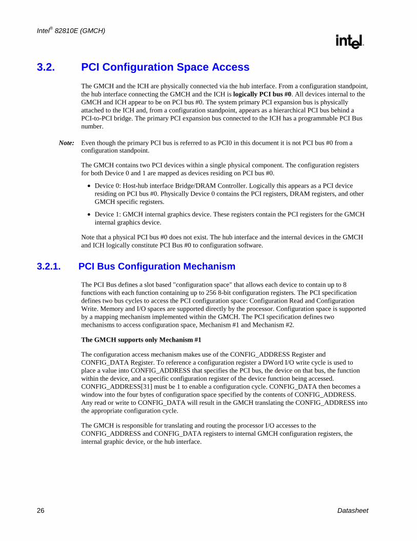
3.2. PCI Configuration Space Access The GMCH and the ICH are physically connected via the hub interface. From a configuration standpoint, the hub interface connecting the GMCH and the ICH is logically PCI bus #0. All devices internal to the GMCH and ICH appear to be on PCI bus #0. The system primary PCI expansion bus is physically attached to the ICH and, from a configuration standpoint, appears as a hierarchical PCI bus behind a PCI-to-PCI bridge. The primary PCI expansion bus connected to the ICH has a programmable PCI Bus number.
Note: Even though the primary PCI bus is referred to as PCI0 in this document it is not PCI bus #0 from a configuration standpoint.
The GMCH contains two PCI devices within a single physical component. The configuration registers for both Device 0 and 1 are mapped as devices residing on PCI bus #0.
• Device 0: Host-hub interface Bridge/DRAM Controller. Logically this appears as a PCI device residing on PCI bus #0. Physically Device 0 contains the PCI registers, DRAM registers, and other GMCH specific registers.
• Device 1: GMCH internal graphics device. These registers contain the PCI registers for the GMCH internal graphics device.
Note that a physical PCI bus #0 does not exist. The hub interface and the internal devices in the GMCH and ICH logically constitute PCI Bus #0 to configuration software.
3.2.1. PCI Bus Configuration Mechanism
The PCI Bus defines a slot based "configuration space" that allows each device to contain up to 8 functions with each function containing up to 256 8-bit configuration registers. The PCI specification defines two bus cycles to access the PCI configuration space: Configuration Read and Configuration Write. Memory and I/O spaces are supported directly by the processor. Configuration space is supported by a mapping mechanism implemented within the GMCH. The PCI specification defines two mechanisms to access configuration space, Mechanism #1 and Mechanism #2.
The GMCH supports only Mechanism #1
The configuration access mechanism makes use of the CONFIG_ADDRESS Register and CONFIG_DATA Register. To reference a configuration register a DWord I/O write cycle is used to place a value into CONFIG_ADDRESS that specifies the PCI bus, the device on that bus, the function within the device, and a specific configuration register of the device function being accessed. CONFIG_ADDRESS[31] must be 1 to enable a configuration cycle. CONFIG_DATA then becomes a window into the four bytes of configuration space specified by the contents of CONFIG_ADDRESS. Any read or write to CONFIG_DATA will result in the GMCH translating the CONFIG_ADDRESS into the appropriate configuration cycle.
The GMCH is responsible for translating and routing the processor I/O accesses to the CONFIG_ADDRESS and CONFIG_DATA registers to internal GMCH configuration registers, the internal graphic device, or the hub interface.
Intel® 82810E (GMCH)
R
Datasheet 27
3.2.2. Logical PCI Bus #0 Configuration Mechanism
The GMCH decodes the Bus Number (bits 23:16) and the Device Number fields of the CONFIG_ADDRESS register. If the Bus Number field of CONFIG_ADDRESS is 0 the configuration cycle is targeting a PCI Bus #0 device.
• Device #0: The Host-hub interface Bridge/DRAM Controller entity within the GMCH is hardwired as Device #0 on PCI Bus #0.
• Device #1: The internal graphics device entity within the GMCH is hardwired as Device #1 on PCI Bus #0. Configuration cycles to one of the GMCH internal devices are confined to the GMCH and not sent over the hub interface. Note: Accesses to devices #2 to #31 on PCI Bus #0 will be forwarded over the hub interface.
3.2.3. Primary PCI (PCI0) and Downstream Configuration Mechanism
If the Bus Number in the CONFIG_ADDRESS register is non-zero the GMCH will generate a configuration cycle over the hub interface. The ICH compares the non-zero Bus Number with the Secondary Bus Number and Subordinate Bus Number registers of its P2P bridges to determine if the configuration cycle is meant for Primary PCI (PCI0), or a downstream PCI bus.
3.2.4. Internal Graphics Device Configuration Mechanism
From the chipset configuration perspective the internal graphics device is seen as a PCI device (device #1) on PCI Bus #0. Configuration cycles that target device #1 on PCI Bus #0 are claimed by the internal graphics device and are not forwarded via hub interface to the ICH.
3.2.5. GMCH Register Introduction
The GMCH contains two sets of software accessible registers, accessed via the Host I/O address space:
• Control registers I/O mapped into the host I/O space, that control access to PCI configuration space (see section entitled I/O Mapped Registers)
• Internal configuration registers residing within the GMCH are partitioned into two logical device register sets (“logical” since they reside within a single physical device). The first register set is dedicated to Host-hub interface Bridge/DRAM Controller functionality (controls PCI0 such as DRAM configuration, other chip-set operating parameters and optional features). The second register block is dedicated to the internal graphics device in the GMCH.
The GMCH supports PCI configuration space accesses using the mechanism denoted as Configuration Mechanism #1 in the PCI specification.
The GMCH internal registers (both I/O Mapped and Configuration registers) are accessible by the host. The registers can be accessed as Byte, Word (16-bit), or DWord (32-bit) quantities, with the exception of CONFIG_ADDRESS register that can only be accessed as a DWord. All multi-byte numeric fields use "little-endian" ordering (i.e., lower addresses contain the least significant parts of the field).
Intel® 82810E (GMCH)
R
28 Datasheet
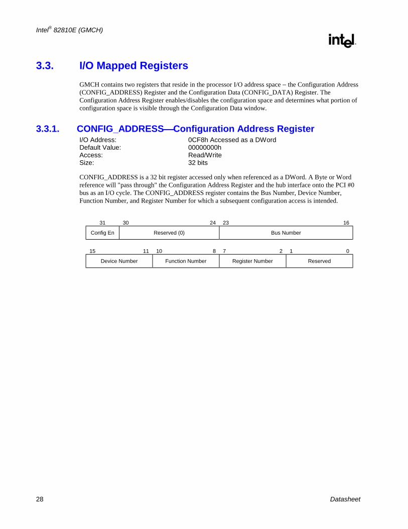
3.3. I/O Mapped Registers GMCH contains two registers that reside in the processor I/O address space − the Configuration Address (CONFIG_ADDRESS) Register and the Configuration Data (CONFIG_DATA) Register. The Configuration Address Register enables/disables the configuration space and determines what portion of configuration space is visible through the Configuration Data window.
3.3.1. CONFIG_ADDRESSConfiguration Address Register I/O Address: 0CF8h Accessed as a DWord Default Value: 00000000h Access: Read/Write Size: 32 bits
CONFIG_ADDRESS is a 32 bit register accessed only when referenced as a DWord. A Byte or Word reference will "pass through" the Configuration Address Register and the hub interface onto the PCI #0 bus as an I/O cycle. The CONFIG_ADDRESS register contains the Bus Number, Device Number, Function Number, and Register Number for which a subsequent configuration access is intended.
31 30 24 23 16
Config En Reserved (0) Bus Number
15 11 10 8 7 2 1 0
Device Number Function Number Register Number Reserved
Intel® 82810E (GMCH)
R
Datasheet 29
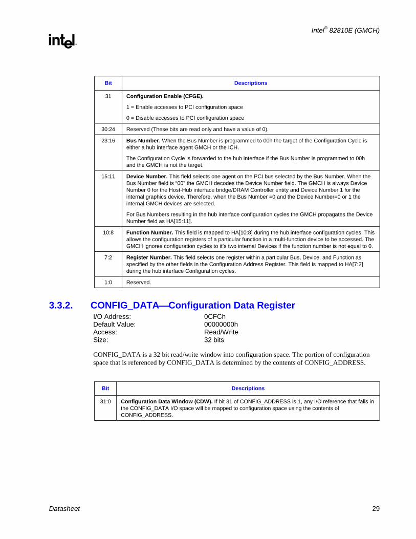
Bit Descriptions
31 Configuration Enable (CFGE).
1 = Enable accesses to PCI configuration space
0 = Disable accesses to PCI configuration space
30:24 Reserved (These bits are read only and have a value of 0).
23:16 Bus Number. When the Bus Number is programmed to 00h the target of the Configuration Cycle is either a hub interface agent GMCH or the ICH.
The Configuration Cycle is forwarded to the hub interface if the Bus Number is programmed to 00h and the GMCH is not the target.
15:11 Device Number. This field selects one agent on the PCI bus selected by the Bus Number. When the Bus Number field is “00” the GMCH decodes the Device Number field. The GMCH is always Device Number 0 for the Host-Hub interface bridge/DRAM Controller entity and Device Number 1 for the internal graphics device. Therefore, when the Bus Number =0 and the Device Number=0 or 1 the internal GMCH devices are selected.
For Bus Numbers resulting in the hub interface configuration cycles the GMCH propagates the Device Number field as HA[15:11].
10:8 Function Number. This field is mapped to HA[10:8] during the hub interface configuration cycles. This allows the configuration registers of a particular function in a multi-function device to be accessed. The GMCH ignores configuration cycles to it’s two internal Devices if the function number is not equal to 0.
7:2 Register Number. This field selects one register within a particular Bus, Device, and Function as specified by the other fields in the Configuration Address Register. This field is mapped to HA[7:2] during the hub interface Configuration cycles.
1:0 Reserved.
3.3.2. CONFIG_DATAConfiguration Data Register I/O Address: 0CFCh Default Value: 00000000h Access: Read/Write Size: 32 bits
CONFIG_DATA is a 32 bit read/write window into configuration space. The portion of configuration space that is referenced by CONFIG_DATA is determined by the contents of CONFIG_ADDRESS.
Bit Descriptions
31:0 Configuration Data Window (CDW). If bit 31 of CONFIG_ADDRESS is 1, any I/O reference that falls in the CONFIG_DATA I/O space will be mapped to configuration space using the contents of CONFIG_ADDRESS.

Intel® 82810E (GMCH)
R
30 Datasheet
3.4. Host-Hub Interface Bridge/DRAM Controller Device Registers (Device 0) Table 3 shows the GMCH configuration space for device #0.
Table 3. GMCH PCI Configuration Space (Device 0)
Address Offset
Register Symbol
Register Name Default Value Access
00–01h VID Vendor Identification 8086h RO
02–03h DID Device Identification 7124 RO
04–05h PCICMD PCI Command Register 0006h R/W
06–07h PCISTS PCI Status Register 0080h RO, R/WC
08h RID Revision Identification 03h RO
09h Reserved 00h
0Ah SUBC Sub-Class Code 00h RO
0Bh BCC Base Class Code 06h RO
0Ch Reserved 00h
0Dh MLT Master Latency Timer 00h RO
0Eh HDR Header Type 00h RO
0Fh Reserved
10–2Bh Reserved
2C–2Dh SVID Subsystem Vendor Identification 0000h R/WO
2E–2Fh SID Subsystem Identification 0000h R/WO
30–33h Reserved
34h CAPPTR Capabilities Pointer 00h RO
35–4Fh Reserved
50h GMCHCFG GMCH Configuration 60h R/W
51h PAM Programmable Attributes 00h R/W
52h DRP DRAM Row Population 00h R/W
53h DRAMT DRAM Timing Register 08h R/W
54–57h Reserved
58h FDHC Fixed DRAM Hole Control 00h R/W
58–6Fh Reserved
70h SMRAM System Management RAM Control 00h R/W
72–73h MISSC Miscellaneous Control 0000h R/W
74–7Fh Reserved
80h MISSC2 Miscellaneous Control 2 00h R/W
81–91h Reserved
92–93h BSC Buffer Strength Control FFFFh R/W
94–FFh Reserved

Intel® 82810E (GMCH)
R
Datasheet 31
3.4.1. VIDVendor Identification Register (Device 0) Address Offset: 00–01h Default Value: 8086h Attribute: Read Only Size: 16 bits
The VID Register contains the vendor identification number. This 16-bit register combined with the Device Identification Register uniquely identify any PCI device. Writes to this register have no effect.
Bit Description
15:0 Vendor Identification Number. This is a 16-bit value assigned to Intel. Intel VID = 8086h.
3.4.2. DIDDevice Identification Register (Device 0) Address Offset: 02–03h Default Value: 7124h Attribute: Read Only Size: 16 bits
This 16-bit register combined with the Vendor Identification register uniquely identifies any PCI device. Writes to this register have no effect.
Bit Description
15:0 Device Identification Number. This is a 16 bit value assigned to the GMCH Host-hub interface Bridge/DRAM Controller Device #0.
Intel® 82810E (GMCH)
R
32 Datasheet
3.4.3. PCICMDPCI Command Register (Device 0) Address Offset: 04–05h Default: 0006h Access: Read/Write Size 16 bits
This 16-bit register provides basic control over the GMCH PCI0 (i.e., Hub-Interface) interface’s ability to respond to Hub Interface cycles.
15 10 9 8
Reserved (0) FB2B (Not Impl)
SERR En
7 6 5 4 3 2 1 0
Addr/Data Stepping (Not Impl)
Parity Error En
(Not Impl)
VGA Pal Sn
(Not Impl)
Mem WR & Inval En (Not Impl)
Special Cycle En (Not Impl)
Bus Master En (Not Impl)
Mem AccEn
(Not Impl)
I/O AccEn (Not Impl)
Bit Descriptions
15:10 Reserved.
9 Fast Back-to-Back. (Not implemented; hardwired to 0). Writes to this bit position have no effect
8 SERR Enable (SERRE). This bit is a global enable bit for Device #0 SERR messaging. The GMCH does not have an SERR# signal. The GMCH communicates the SERR condition by sending an SERR message to the ICH. If this bit is set to a 1, the GMCH is enabled to generate SERR messages over the hub interface for specific Device #0 error conditions (Note: the only SERR condition for the GMCH is Received Target Abort, therefore there are no other SERR enable bits in the GMCH ). If SERRE is reset to 0, then the SERR message is not generated by the GMCH for Device #0.
NOTE: This bit only controls SERR messaging for the Device #0.
7 Address/Data Stepping. (Not implemented; hardwired to 0). Writes to this bit position have no effect.
6 Parity Error Enable (PERRE). (Not implemented; hardwired to 0). Writes to this bit position have no effect.
5 VGA Palette Snoop. (Not implemented, hardwired to 0). Writes to this bit position have no effect
4 Memory Write and Invalidate Enable. (Not implemented; hardwired to 0). Writes to this bit position have no effect
3 Special Cycle Enable. (Not implemented; hardwired to 0). Writes to this bit position have no effect
2 Bus Master Enable (BME). (Not implemented: hardwired to 1). GMCH is always a Bus Master. Writes to this bit position have no effect
1 Memory Access Enable (MAE). (Not implemented; hardwired to 1). Writes to this bit position have no effect
0 I/O Access Enable (IOAE). (Not implemented: hardwired to 0). Writes to this bit position have no effect

Intel® 82810E (GMCH)
R
Datasheet 33
3.4.4. PCISTSPCI Status Register (Device 0) Address Offset: 06–07h Default Value: 0080h Access: Read Only, Read/Write Clear Size: 16 bits
PCISTS is a 16 bit status register that reports the occurrence of error events on the hub interface.
15 14 13 12 11 10 9 8
Detected Par Error (HW=0)
Sig Sys Error
Recog Mast Abort
Sta
Rec Target
Abort Sta (HW=0)
Sig Target Abort Sta (HW=0)
DEVSEL# Timing (HW=00)
Data Par Detected (HW=0)
7 6 5 4 3 0
FB2B (HW=1)
Reserved Cap List (HW=0)
Reserved
Bit Descriptions
15 Detected Parity Error (DPE)—RO. This bit is hardwired to 0. Writes to this bit position have no effect.
14 Signaled System Error (SSE)—RWC. (Note: the only SERR condition for GMCH is Received Target Abort; therefore, there are no other SERR enable bits in the GMCH ).
1 = GMCH Device #0 generated an SERR message over hub interface for any enabled Device #0 error condition. Device #0 error conditions are enabled in the PCICMD register. Device #0 error flags are read/reset from the PCISTS register.
0 = Software sets SSE to 0 by writing a 1 to this bit.
13 Received Master Abort Status (RMAS)—RWC. 1 = GMCH generated a Hub-Interface request that receives a Master Abort completion packet.
0 = Software clears this bit by writing a 1 to it.
12 Received Target Abort Status (RTAS)—RWC. 1 = GMCH generated a Hub Interface request that receives a Target Abort completion packet.
0 = Software clears this bit by writing a 1 to it.
11 Signaled Target Abort Status (STAS)—RO. (Not implemented; hardwired to a 0). Writes to this bit position have no effect.
10:9 DEVSEL# Timing (DEVT)—RO. These bits are hardwired to “00”. Writes to these bit positions have no effect. Device #0 does not physically connect to PCI0. These bits are set to “00” (fast decode) so that optimum DEVSEL timing for PCI0 is not limited by the GMCH.
8 Data Parity Detected (DPD)—RO. Hardwired to a 0. Writes to this bit position have no effect.
7 Fast Back-to-Back (FB2B)—RO. Hardwired to 1. Writes to these bit positions have no effect. Device #0 does not physically connect to PCI. This bit is set to 1 (indicating fast back-to-back capability) so that the optimum setting for PCI is not limited by the GMCH.
6:5 Reserved.
4 Capability List (CLIST)—RO. This bit is hardwired to 0, to indicate to the configuration software that this device/function does not implement a new list of features, and that there is NO CAPPTR.
3:0 Reserved.

Intel® 82810E (GMCH)
R
34 Datasheet
3.4.5. RIDRevision Identification Register (Device 0) Address Offset: 08h Default Value: 03h Access: Read Only Size: 8 bits
This register contains the revision number of the GMCH Device 0. These bits are read only and writes to this register have no effect.
Bit Description
7:0 Revision Identification Number. This is an 8-bit value that indicates the revision identification number for the GMCH device #0.
For 810E, this value is 03h.
3.4.6. SUBCSub-Class Code Register (Device 0) Address Offset: 0Ah Default Value: 00h Access: Read Only Size: 8 bits
This register contains the Sub-Class Code for the GMCH Device #0. This code is 00h indicating a Host Bridge device. The register is read only.
Bit Description
7:0 Sub-Class Code (SUBC). This is an 8-bit value that indicates the category of Bridge into which the GMCH falls.
00h = Host Bridge.
3.4.7. BCCBase Class Code Register (Device 0) Address Offset: 0Bh Default Value: 06h Access: Read Only Size: 8 bits
This register contains the Base Class Code of the GMCH Device #0. This code is 06h indicating a Bridge device. This register is read only.
Bit Description
7:0 Base Class Code (BASEC). This is an 8-bit value that indicates the Base Class Code for the GMCH.
06h = Bridge device.

Intel® 82810E (GMCH)
R
Datasheet 35
3.4.8. MLTMaster Latency Timer Register (Device 0) Address Offset: 0Dh Default Value: 00h Access: Read Only Size: 8 bits
MLT Function has moved to the ICH; therefore, this register is not implemented in the GMCH.
Bit Descriptions
7:0 Master Latency Timer Value. This read only field always returns 0’s.
3.4.9. HDRHeader Type Register (Device 0) Offset: 0Eh Default: 00h Access: Read Only Size: 8 bits
This register identifies the header layout of the configuration space. No physical register exists at this location.
Bit Descriptions
7:0 Header Type. This read only field always returns 0’s.
3.4.10. SVIDSubsystem Vendor Identification Register (Device 0) Offset: 2C–2Dh Default: 0000h Access: Read/Write Once Size: 16 bits
Bit Description
15:0 Subsystem Vendor ID—R/WO. This value is used to identify the vendor of the subsystem. This field should be programmed by BIOS during boot-up. Once written, this register becomes read only. This register can only be cleared by a reset.
Intel® 82810E (GMCH)
R
36 Datasheet
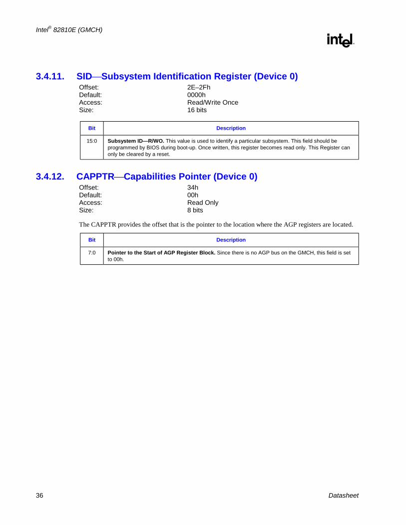
3.4.11. SIDSubsystem Identification Register (Device 0) Offset: 2E–2Fh Default: 0000h Access: Read/Write Once Size: 16 bits
Bit Description
15:0 Subsystem ID—R/WO. This value is used to identify a particular subsystem. This field should be programmed by BIOS during boot-up. Once written, this register becomes read only. This Register can only be cleared by a reset.
3.4.12. CAPPTRCapabilities Pointer (Device 0) Offset: 34h Default: 00h Access: Read Only Size: 8 bits
The CAPPTR provides the offset that is the pointer to the location where the AGP registers are located.
Bit Description
7:0 Pointer to the Start of AGP Register Block. Since there is no AGP bus on the GMCH, this field is set to 00h.
Intel® 82810E (GMCH)
R
Datasheet 37
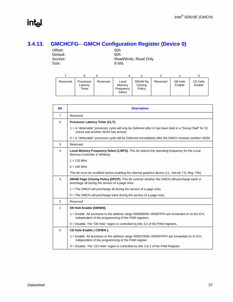
3.4.13. GMCHCFGGMCH Configuration Register (Device 0) Offset: 50h Default: 60h Access: Read/Write, Read Only Size: 8 bits
7 6 5 4 3 2 1 0
Reserved Processor Latency Timer
Reserved Local Memory
Frequency Select
DRAM Pg Closing Policy
Reserved D8 Hole Enable
CD Hole Enable
Bit Description
7 Reserved
6 Processor Latency Timer (CLT).
1 = A “deferrable” processor cycle will only be Deferred after in has been held in a “Snoop Stall” for 31 clocks and another ADS# has arrived.
0 = A “deferrable” processor cycle will be Deferred immediately after the GMCH receives another ADS#
5 Reserved
4 Local Memory Frequency Select (LMFS). This bit selects the operating frequency for the Local Memory Controller in Whitney
1 = 133 MHz
0 = 100 MHz
This bit must be modified before enabling the internal graphics device (i.e., bits bit 7:6, Reg. 70h)
3 DRAM Page Closing Policy (DPCP). This bit controls whether the GMCH will precharge bank or precharge all during the service of a page miss.
1 = The GMCH will prechange all during the service of a page miss.
0 = The GMCH will prechange bank during the service of a page miss.
2 Reserved
1 D8 Hole Enable (D8HEN).
1 = Enable. All accesses to the address range 000D8000h–000DFFFh are forwarded on to the ICH, independent of the programming of the PAM registers.
0 = Disable. The “D8 Hole” region is controlled by bits 3:2 of the PAM registers.
0 CD Hole Enable ( CDHEN ).
1 = Enable. All accesses to the address range 000DC000h–000DFFFFh are forwarded on to ICH, independent of the programming of the PAM register.
0 = Disable. The “CD Hole” region is controlled by bits 3 & 2 of the PAM Register.
Intel® 82810E (GMCH)
R
38 Datasheet
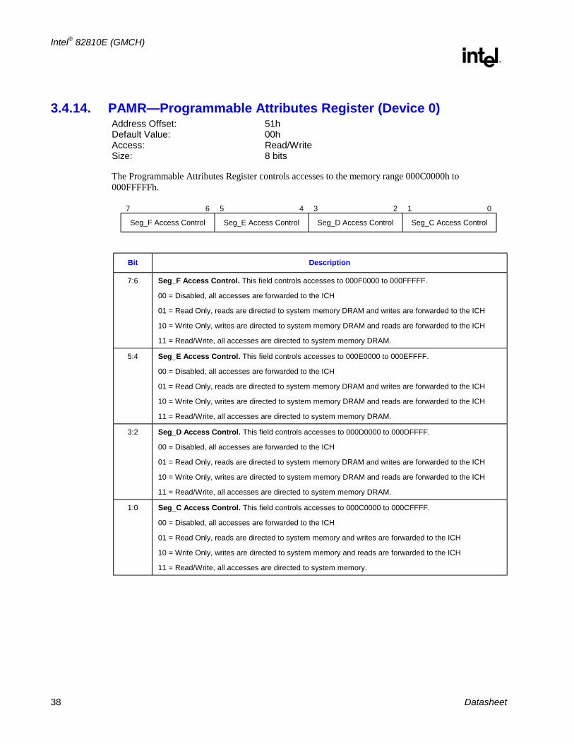
3.4.14. PAMR—Programmable Attributes Register (Device 0) Address Offset: 51h Default Value: 00h Access: Read/Write Size: 8 bits
The Programmable Attributes Register controls accesses to the memory range 000C0000h to 000FFFFFh.
7 6 5 4 3 2 1 0
Seg_F Access Control Seg_E Access Control Seg_D Access Control Seg_C Access Control
Bit Description
7:6 Seg_F Access Control. This field controls accesses to 000F0000 to 000FFFFF.
00 = Disabled, all accesses are forwarded to the ICH
01 = Read Only, reads are directed to system memory DRAM and writes are forwarded to the ICH
10 = Write Only, writes are directed to system memory DRAM and reads are forwarded to the ICH
11 = Read/Write, all accesses are directed to system memory DRAM.
5:4 Seg_E Access Control. This field controls accesses to 000E0000 to 000EFFFF.
00 = Disabled, all accesses are forwarded to the ICH
01 = Read Only, reads are directed to system memory DRAM and writes are forwarded to the ICH
10 = Write Only, writes are directed to system memory DRAM and reads are forwarded to the ICH
11 = Read/Write, all accesses are directed to system memory DRAM.
3:2 Seg_D Access Control. This field controls accesses to 000D0000 to 000DFFFF.
00 = Disabled, all accesses are forwarded to the ICH
01 = Read Only, reads are directed to system memory DRAM and writes are forwarded to the ICH
10 = Write Only, writes are directed to system memory DRAM and reads are forwarded to the ICH
11 = Read/Write, all accesses are directed to system memory DRAM.
1:0 Seg_C Access Control. This field controls accesses to 000C0000 to 000CFFFF.
00 = Disabled, all accesses are forwarded to the ICH
01 = Read Only, reads are directed to system memory and writes are forwarded to the ICH
10 = Write Only, writes are directed to system memory and reads are forwarded to the ICH
11 = Read/Write, all accesses are directed to system memory.
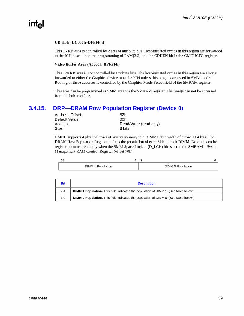
Intel® 82810E (GMCH)
R
Datasheet 39
CD Hole (DC000h–DFFFFh)
This 16 KB area is controlled by 2 sets of attribute bits. Host-initiated cycles in this region are forwarded to the ICH based upon the programming of PAM[3:2] and the CDHEN bit in the GMCHCFG register.
Video Buffer Area (A0000h–BFFFFh)
This 128 KB area is not controlled by attribute bits. The host-initiated cycles in this region are always forwarded to either the Graphics device or to the ICH unless this range is accessed in SMM mode. Routing of these accesses is controlled by the Graphics Mode Select field of the SMRAM register.
This area can be programmed as SMM area via the SMRAM register. This range can not be accessed from the hub interface.
3.4.15. DRPDRAM Row Population Register (Device 0) Address Offset: 52h Default Value: 00h Access: Read/Write (read only) Size: 8 bits
GMCH supports 4 physical rows of system memory in 2 DIMMs. The width of a row is 64 bits. The DRAM Row Population Register defines the population of each Side of each DIMM. Note: this entire register becomes read only when the SMM Space Locked (D_LCK) bit is set in the SMRAMSystem Management RAM Control Register (offset 70h).
15 4 3 0
DIMM 1 Population DIMM 0 Population
Bit Description
7:4 DIMM 1 Population. This field indicates the population of DIMM 1. (See table below )
3:0 DIMM 0 Population. This field indicates the population of DIMM 0. (See table below )
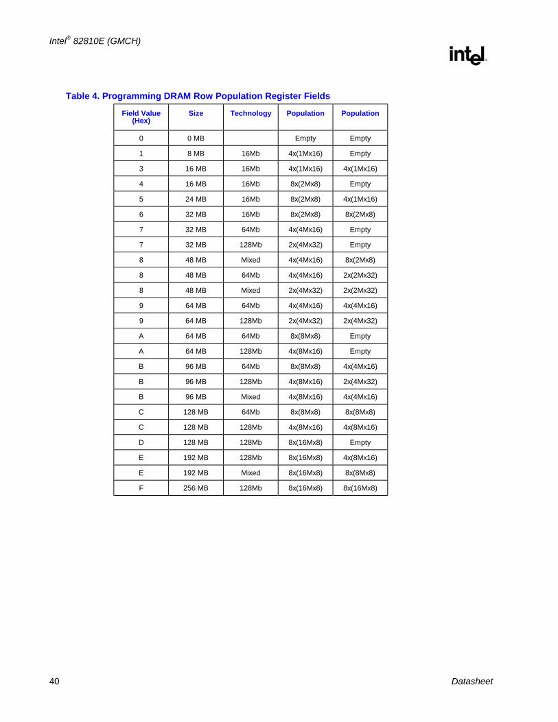
Intel® 82810E (GMCH)
R
40 Datasheet
Table 4. Programming DRAM Row Population Register Fields
Field Value (Hex)
Size Technology Population Population
0 0 MB Empty Empty
1 8 MB 16Mb 4x(1Mx16) Empty
3 16 MB 16Mb 4x(1Mx16) 4x(1Mx16)
4 16 MB 16Mb 8x(2Mx8) Empty
5 24 MB 16Mb 8x(2Mx8) 4x(1Mx16)
6 32 MB 16Mb 8x(2Mx8) 8x(2Mx8)
7 32 MB 64Mb 4x(4Mx16) Empty
7 32 MB 128Mb 2x(4Mx32) Empty
8 48 MB Mixed 4x(4Mx16) 8x(2Mx8)
8 48 MB 64Mb 4x(4Mx16) 2x(2Mx32)
8 48 MB Mixed 2x(4Mx32) 2x(2Mx32)
9 64 MB 64Mb 4x(4Mx16) 4x(4Mx16)
9 64 MB 128Mb 2x(4Mx32) 2x(4Mx32)
A 64 MB 64Mb 8x(8Mx8) Empty
A 64 MB 128Mb 4x(8Mx16) Empty
B 96 MB 64Mb 8x(8Mx8) 4x(4Mx16)
B 96 MB 128Mb 4x(8Mx16) 2x(4Mx32)
B 96 MB Mixed 4x(8Mx16) 4x(4Mx16)
C 128 MB 64Mb 8x(8Mx8) 8x(8Mx8)
C 128 MB 128Mb 4x(8Mx16) 4x(8Mx16)
D 128 MB 128Mb 8x(16Mx8) Empty
E 192 MB 128Mb 8x(16Mx8) 4x(8Mx16)
E 192 MB Mixed 8x(16Mx8) 8x(8Mx8)
F 256 MB 128Mb 8x(16Mx8) 8x(16Mx8)
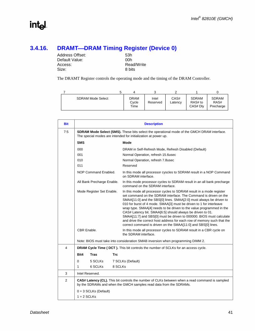
Intel® 82810E (GMCH)
R
Datasheet 41
3.4.16. DRAMTDRAM Timing Register (Device 0) Address Offset: 53h Default Value: 00h Access: Read/Write Size: 8 bits
The DRAMT Register controls the operating mode and the timing of the DRAM Controller.
7 5 4 3 2 1 0
SDRAM Mode Select DRAM Cycle Time
Intel Reserved
CAS# Latency
SDRAM RAS# to
CAS# Dly
SDRAM RAS#
Precharge
Bit Description
7:5 SDRAM Mode Select (SMS). These bits select the operational mode of the GMCH DRAM interface. The special modes are intended for initialization at power up.
SMS Mode
000 DRAM in Self-Refresh Mode, Refresh Disabled (Default) 001 Normal Operation, refresh 15.6usec 010 Normal Operation, refresh 7.8usec 011 Reserved
NOP Command Enabled. In this mode all processor cyscles to SDRAM result in a NOP Command on SDRAM interface.
All Bank Precharge Enable. In this mode processor cycles to SDRAM result in an all bank precharge command on the SDRAM interface.
Mode Register Set Enable. In this mode all processor cycles to SDRAM result in a mode register set command on the SDRAM interface. The Command is driven on the SMAA[11:0] and the SBS[0] lines. SMAA[2:0] must always be driven to 010 for burst of 4 mode. SMAA[3] must be driven to 1 for interleave wrap type. SMAA[4] needs to be driven to the value programmed in the CAS# Latency bit. SMAA[6:5] should always be driven to 01. SMAA[11:7] and SBS[0] must be driven to 000000. BIOS must calculate and drive the correct host address for each row of memory such that the correct command is driven on the SMAA[11:0] and SBS[0] lines.
CBR Enable. In this mode all processor cycles to SDRAM result in a CBR cycle on the SDRAM interface.
Note: BIOS must take into consideration SMAB inversion when programming DIMM 2.
4 DRAM Cycle Time ( DCT ). This bit controls the number of SCLKs for an access cycle.
Bit4 Tras Trc
0 5 SCLKs 7 SCLKs (Default) 1 6 SCLKs 8 SCLKs
3 Intel Reserved.
2 CAS# Latency (CL). This bit controls the number of CLKs between when a read command is sampled by the SDRAMs and when the GMCH samples read data from the SDRAMs.
0 = 3 SCLKs (Default) 1 = 2 SCLKs
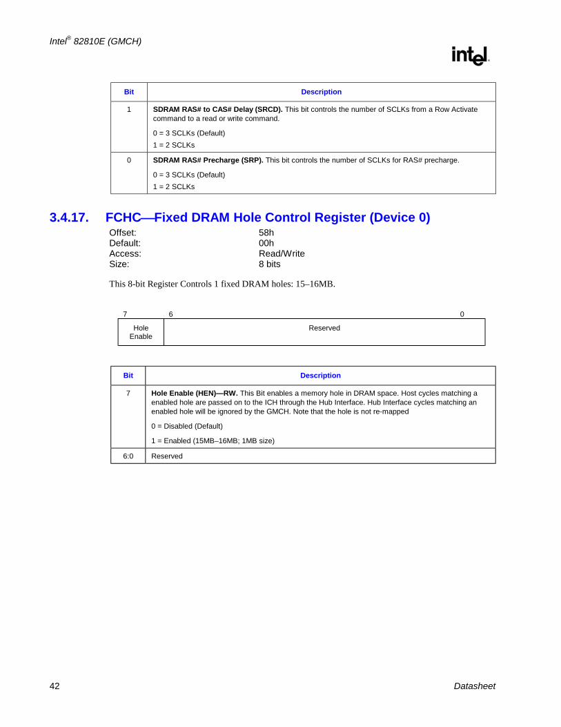
Intel® 82810E (GMCH)
R
42 Datasheet
Bit Description
1 SDRAM RAS# to CAS# Delay (SRCD). This bit controls the number of SCLKs from a Row Activate command to a read or write command.
0 = 3 SCLKs (Default) 1 = 2 SCLKs
0 SDRAM RAS# Precharge (SRP). This bit controls the number of SCLKs for RAS# precharge.
0 = 3 SCLKs (Default) 1 = 2 SCLKs
3.4.17. FCHCFixed DRAM Hole Control Register (Device 0) Offset: 58h Default: 00h Access: Read/Write Size: 8 bits
This 8-bit Register Controls 1 fixed DRAM holes: 15–16MB.
7 6 0
Hole Enable
Reserved
Bit Description
7 Hole Enable (HEN)—RW. This Bit enables a memory hole in DRAM space. Host cycles matching a enabled hole are passed on to the ICH through the Hub Interface. Hub Interface cycles matching an enabled hole will be ignored by the GMCH. Note that the hole is not re-mapped
0 = Disabled (Default)
1 = Enabled (15MB–16MB; 1MB size)
6:0 Reserved

Intel® 82810E (GMCH)
R
Datasheet 43
3.4.18. SMRAMSystem Management RAM Control Register (Device 0) Address Offset: 70h Default Value: 00h Access: Read/Write Size: 8 bits
The SMRAM register controls how accesses to Compatible and Extended SMRAM spaces are treated, and how much (if any) memory used from the System to support both SMRAM and Graphics Local Memory needs.
7 6 5 4 3 2 1 0
Graphics Mode Select Upper SMM Select Lower SMM Select SMM Space Locked
E_SMRAM_ERR
Bit Description
7:6 Graphics Mode Select (GMS). This field is used to enable/disable the internal graphics device and select the amount of system memory that is used to support the internal graphics device.
00 = Graphics Device Disabled, No memory used (Device 1 is not accessible in this case)
01 = Reserved
10 = Graphics Device Enabled, 512 KB of memory used
11 = Graphics Device Enabled 1 MB of memory used
Note: When the Graphics Device is Disabled (00) the graphics device and all of its memory and I/O functions are disabled and the clocks to this logic are turned off, memory accesses to the VGA range.
The 512 KB and 1 MB space selected by this field is used by video BIOS for handling support of VGA when no GMCH graphics driver is present (e.g., a DOS boot).
(A0000h–BFFFFh) will be forwarded on to the hub interface, and no system memory is used to support the internal graphics device. When this field is non-zero the graphics device of the GMCH and all of its memory and I/O functions are enabled, all non-SMM memory accesses to the VGA range will be handled internally and the selected amount of system memory (0, 512K or 1M) is used from system memory to support the internal graphics device.
Once D_LCK is set, these bits becomes read only.
5:4 Upper SMM Select ( USMM ). This field is used to enable/disable the various SMM memory ranges above 1 MB. TSEG is a block of memory (Used from System Memory at [TOM-Size] : [TOM]) that is only accessible by the processor and only while operating in SMM mode. HSEG is a Remap of the AB segment at FEEA0000 : FEEBFFFF. Both of these areas, when enabled, are usable as SMM RAM, Non-SMM Operations that use these address ranges are forwarded to hub interface. HSEG is ONLY enabled if LSMM = 00.
00 = TSEG and HSEG are both Disabled
01 = TSEG is Disabled, HSEG is Conditionally Enabled
10 = TSEG is Enabled as 512 KB and HSEG is Conditionally Enabled
11 = TSEG is Enabled as 1 MB and HSEG is Conditionally Enabled
Once D_LCK is set, these bits becomes read only.
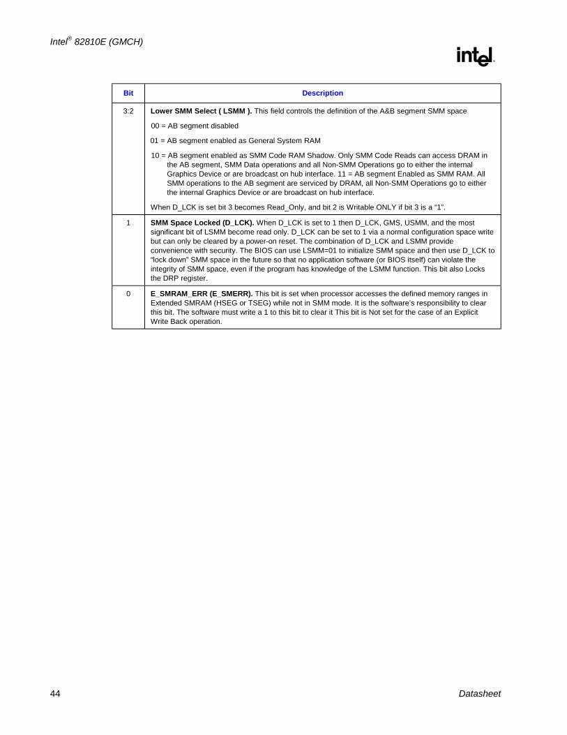
Intel® 82810E (GMCH)
R
44 Datasheet
Bit Description
3:2 Lower SMM Select ( LSMM ). This field controls the definition of the A&B segment SMM space
00 = AB segment disabled
01 = AB segment enabled as General System RAM
10 = AB segment enabled as SMM Code RAM Shadow. Only SMM Code Reads can access DRAM in the AB segment, SMM Data operations and all Non-SMM Operations go to either the internal Graphics Device or are broadcast on hub interface. 11 = AB segment Enabled as SMM RAM. All SMM operations to the AB segment are serviced by DRAM, all Non-SMM Operations go to either the internal Graphics Device or are broadcast on hub interface.
When D_LCK is set bit 3 becomes Read_Only, and bit 2 is Writable ONLY if bit 3 is a “1”.
1 SMM Space Locked (D_LCK). When D_LCK is set to 1 then D_LCK, GMS, USMM, and the most significant bit of LSMM become read only. D_LCK can be set to 1 via a normal configuration space write but can only be cleared by a power-on reset. The combination of D_LCK and LSMM provide convenience with security. The BIOS can use LSMM=01 to initialize SMM space and then use D_LCK to “lock down” SMM space in the future so that no application software (or BIOS itself) can violate the integrity of SMM space, even if the program has knowledge of the LSMM function. This bit also Locks the DRP register.
0 E_SMRAM_ERR (E_SMERR). This bit is set when processor accesses the defined memory ranges in Extended SMRAM (HSEG or TSEG) while not in SMM mode. It is the software’s responsibility to clear this bit. The software must write a 1 to this bit to clear it This bit is Not set for the case of an Explicit Write Back operation.
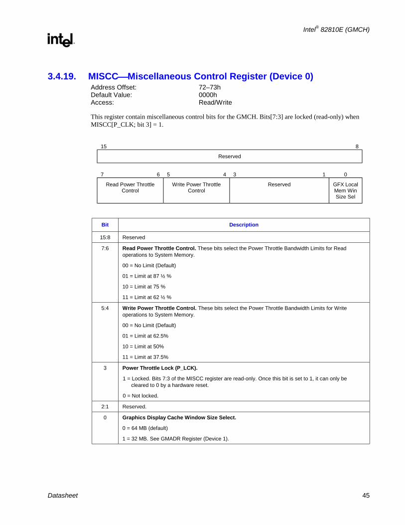
Intel® 82810E (GMCH)
R
Datasheet 45
3.4.19. MISCCMiscellaneous Control Register (Device 0) Address Offset: 72–73h Default Value: 0000h Access: Read/Write
This register contain miscellaneous control bits for the GMCH. Bits[7:3] are locked (read-only) when MISCC[P_CLK; bit 3] = 1.
15 8
Reserved
7 6 5 4 3 1 0
Read Power Throttle Control
Write Power Throttle Control
Reserved GFX Local Mem Win Size Sel
Bit Description
15:8 Reserved
7:6 Read Power Throttle Control. These bits select the Power Throttle Bandwidth Limits for Read operations to System Memory.
00 = No Limit (Default)
01 = Limit at 87 ½ %
10 = Limit at 75 %
11 = Limit at 62 ½ %
5:4 Write Power Throttle Control. These bits select the Power Throttle Bandwidth Limits for Write operations to System Memory.
00 = No Limit (Default)
01 = Limit at 62.5%
10 = Limit at 50%
11 = Limit at 37.5%
3 Power Throttle Lock (P_LCK).
1 = Locked. Bits 7:3 of the MISCC register are read-only. Once this bit is set to 1, it can only be cleared to 0 by a hardware reset.
0 = Not locked.
2:1 Reserved.
0 Graphics Display Cache Window Size Select.
0 = 64 MB (default)
1 = 32 MB. See GMADR Register (Device 1).

Intel® 82810E (GMCH)
R
46 Datasheet
3.4.20. MISCC2Miscellaneous Control 2 Register (Device 0) Address Offset: 80h Default Value: 00h Access: Read/Write
This register controls miscellaneous functionality in the GMCH.
7 6 5 3 2 1 0
Intel Reserved
(must be 1)
Text Immediate Blit Enable
Reserved Palette Load
Select
Instr. Parser
Unit-Lrvel Clock
Enable
Intel Reserved
Bit Description
7 Intel Reserved. This Bit must be programmed to 1.
Do not program to 0.
6 Text Immediate Blit Enable. This bit controls how the GMCH handles blits. This bit must be programmed to a 1 for proper operation
1 = Enable.
0 = Disable. Do NOT program to 0
5:3 Reserved
2 Palette Load Select. This bit controls how the palette is loaded in the GMCH. This bit must be programmed to 1 for proper operation.
1 = Enable.
0 = Disable. Do NOT program to 0.
1 Instruction Parser Unit-Level Clock Gating Enable. This bit controls the unit-level clock gating in the Instruction Parser. This bit must be programmed to 1 for proper operation.
1= Enable.
0 = Disable. Do NOT program to 0.
0 Reserved

Intel® 82810E (GMCH)
R
Datasheet 47
3.4.21. BUFF_SC—System Memory Buffer Strength Control Register (Device 0) Address Offset: 92–93h Default Value: FFFFh Access: Read/Write
This register programs the system memory DRAM interface signal buffer strengths. The programming of these bits should be based on DRAM density (x8, x16, or x32), DRAM technology (16Mb, 64Mb, 128Mb), rows populated, etc. Note that x4 DRAM and Registered DIMMs are not supported. DIMMs with ECC are not supported. The BIOS, upon detection of ECC via SPD, should report to the user that ECC DIMM timings are not supported by the GMCH.
The GMCH supports 2 DIMM slots with each slot supporting two rows of memory. Slots are numbered 0 through 1. Rows of Slots 0 are numbered 0 through 1. Rows of Slot 1 are numbed 2 through 3. The DIMM’s SPD Byte 5 describes the number of sides in a DIMM; SPD Byte 13 provides information on the DRAM width (x8, x16, or x32). BIOS uses these two SPD bytes to calculate loads on memory signals. Load calculation is made based on populated memory rows.
For GMCH stepping with Revision ID ≥ 02, the default value of this register is FFFFh.The table below is applicable for GMCH stepping with a Revision ID (Register 08h, Dev. 0) greater than 00h.
15 14 13 12 11 10 9 8
SCS0# Buffer
Strength
SCS1# Buffer
Strength
SCS2# Buffer
Strength
SCS3# Buffer
Strength
SMAA[7:4] Buffer Strength
SMAB[7:4] Buffer Strength
7 6 5 4 3 2 1 0
CKE1 Buffer Strength CKE0 Buffer Strength MD and DQM Buffer Strength
Control Buffer Strength
Bit Description
15 SCS0# Buffer Strength. This field sets the buffer strength for system memory chip buffer SCS0#.
0 = 3x: (6 to 8 loads) 1 = 2x: (2 to 4 loads) load = (64 / SDRAM width for Row 0, if populated)
14 SCS1# Buffer Strength. This field sets the buffer strength for system memory chip buffer SCS1#.
0 = 3x: (6 to 8 loads)
1 = 2x: (2 to 4 loads)
load = (64 / SDRAM width for Row 1, if populated)
13 SCS2# Buffer Strength. This field sets the buffer strength for system memory chip buffer SCS2#.
0 = 3x: (6 to 8 loads)
1 = 2x: (2 to 4 loads)
load = (64 / SDRAM width for Row 2, if populated)

Intel® 82810E (GMCH)
R
48 Datasheet
Bit Description
12 SCS3# Buffer Strength. This field sets the buffer strength for system memory chip buffer SCS3#.
0 = 3x: (6 to 8 loads) 1 = 2x: (2 to 4 loads)
load = (64 / SDRAM width for Row 3, if populated)
11:10 SMAA[7:4] Buffer Strength. This field sets the buffer strength for SMAA[7:4] buffers.
00 = 4x: (12 to 16 loads) 01 = 3x: (8 to 10 loads) 10 = 2x: (4 to 6 loads) 11 = 1x: (2 loads) load = (64 / SDRAM width for Row 0, if populated) + (64 / SDRAM width for Row 1, if populated)
9:8 SMAB[7:4] Buffer Strength. This field sets the buffer strength for SMAB[7:4] buffers. 00 = 4x: (12 to 16 loads) 01 = 3x: (8 to 10 loads) 10 = 2x: (4 to 6 loads) 11 = 1x: (2 loads) load = (64 / SDRAM width for Row 2, if populated) + (64 / SDRAM width for Row 3, if populated)
7:6 CKE1 Buffer Strength. This field sets the buffer strength for CKE1 buffers. 00 = 4x: (10 to 16 loads) 01 = 3x: (6 to 8 loads) 10 = 2x: (2 to 4 loads) 11 = 1x: (0 load) Load = (64 / SDRAM width for Row 1, if populated) + (64 / SDRAM width for Row 3, if populated)
5:4 CKE0 Buffer Strength. This field sets the buffer strength for CKE0 buffers.
00 = 4x: (10 to 16 loads) 01 = 3x: (6 to 8 loads) 10 = 2x: (2 to 4 loads) 11 = 1x: (0 load) Load = (64 / SDRAM width for Row 0, if populated) + (64 / SDRAM width for Row 2, if populated)
3:2 SMD [63:0] and SDQM [7:0] Buffer Strength. This field sets the buffer strength for SMD [63:0] and SDQM [7:0] pins.
00 = 2.5x: (4 loads) 01 = 1.5x: (2 to 3 loads) 10 = 1x: (1 load) 11 = 1x: (invalid setting for SDQM[7:0])
Note: BUFF_SC[3:2] = 11 is an invalid state for SDQM[7:0]. For the 1x buffer strength configuration, set BUFF_SC[3:2] = 10.
Load = 1 for each populated row, totaled for all DIMMs
1:0 SWE#, SCAS#, SRAS#, MAA [11:8, 3:0], SBS [1:0] Control Buffer Strength. This field sets the buffer strength for SWE#, SCAS#, SRAS#, MAA [11:8, 3:0], and SBS [1:0] pins.
00 = 4x: (Not Applicable) 01 = 3x: (22 to 32 loads) 10 = 2x: (8 to 20 loads) 11 = 1x: (2 to 6 loads) Load = (64 / SDRAM width for Row 0, if populated) + (64 / SDRAM width for Row 1, if populated) + (64 / SDRAM width for Row 2, if populated) + (64 / SDRAM width for Row 3, if populated)
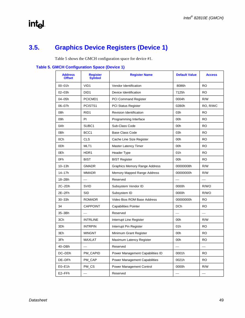
Intel® 82810E (GMCH)
R
Datasheet 49
3.5. Graphics Device Registers (Device 1) Table 5 shows the GMCH configuration space for device #1.
Table 5. GMCH Configuration Space (Device 1)
Address Offset
Register Symbol
Register Name Default Value Access
00–01h VID1 Vendor Identification 8086h RO
02–03h DID1 Device Identification 7125h RO
04–05h PCICMD1 PCI Command Register 0004h R/W
06–07h PCISTS1 PCI Status Register 02B0h RO, R/WC
08h RID1 Revision Identification 03h RO
09h PI Programming Interface 00h RO
0Ah SUBC1 Sub-Class Code 00h RO
0Bh BCC1 Base Class Code 03h RO
0Ch CLS Cache Line Size Register 00h RO
0Dh MLT1 Master Latency Timer 00h RO
0Eh HDR1 Header Type 01h RO
0Fh BIST BIST Register 00h RO
10–13h GMADR Graphics Memory Range Address 00000008h R/W
14–17h MMADR Memory Mapped Range Address 00000000h R/W
18–2Bh Reserved
2C–2Dh SVID Subsystem Vendor ID 0000h R/WO
2E–2Fh SID Subsystem ID 0000h R/WO
30–33h ROMADR Video Bios ROM Base Address 00000000h RO
34 CAPPOINT Capabilities Pointer DCh RO
35–3Bh Reserved
3Ch INTRLINE Interrupt Line Register 00h R/W
3Dh INTRPIN Interrupt Pin Register 01h RO
3Eh MINGNT Minimum Grant Register 00h RO
3Fh MAXLAT Maximum Latency Register 00h RO
40–DBh Reserved
DC–DDh PM_CAPID Power Management Capabilities ID 0001h RO
DE–DFh PM_CAP Power Management Capabilities 0021h RO
E0–E1h PM_CS Power Management Control 0000h R/W
E2–FFh Reserved
Intel® 82810E (GMCH)
R
50 Datasheet
3.5.1. VIDVendor Identification Register (Device 1) Address Offset: 00h−01h Default Value: 8086h Attribute: Read Only
The VID Register contains the vendor identification number. This 16-bit register combined with the Device Identification Register uniquely identify any PCI device. Writes to this register have no effect.
Bit Description
15:0 Vendor Identification Number. This is a 16-bit value assigned to Intel.
3.5.2. DIDDevice Identification Register (Device 1) Address Offset: 02h−03h Default Value: 7125h Attribute: Read Only
This 16-bit register combined with the Vendor Identification register uniquely identifies any PCI device. Writes to this register have no effect.
Bit Description
15:0 Device Identification Number. This is a 16 bit value assigned to the internal graphics device of the GMCH.
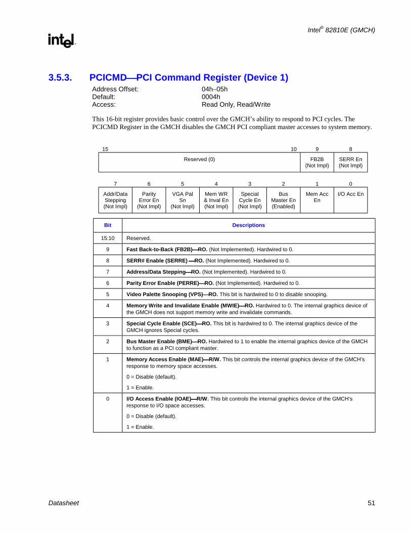
Intel® 82810E (GMCH)
R
Datasheet 51
3.5.3. PCICMDPCI Command Register (Device 1) Address Offset: 04h−05h Default: 0004h Access: Read Only, Read/Write
This 16-bit register provides basic control over the GMCH’s ability to respond to PCI cycles. The PCICMD Register in the GMCH disables the GMCH PCI compliant master accesses to system memory.
15 10 9 8
Reserved (0) FB2B (Not Impl)
SERR En (Not Impl)
7 6 5 4 3 2 1 0
Addr/Data Stepping (Not Impl)
Parity Error En
(Not Impl)
VGA Pal Sn
(Not Impl)
Mem WR & Inval En (Not Impl)
Special Cycle En (Not Impl)
Bus Master En (Enabled)
Mem Acc En
I/O Acc En
Bit Descriptions
15:10 Reserved.
9 Fast Back-to-Back (FB2B)RO. (Not Implemented). Hardwired to 0.
8 SERR# Enable (SERRE) RO. (Not Implemented). Hardwired to 0.
7 Address/Data SteppingRO. (Not Implemented). Hardwired to 0.
6 Parity Error Enable (PERRE)RO. (Not Implemented). Hardwired to 0.
5 Video Palette Snooping (VPS)RO. This bit is hardwired to 0 to disable snooping.
4 Memory Write and Invalidate Enable (MWIE)RO. Hardwired to 0. The internal graphics device of the GMCH does not support memory write and invalidate commands.
3 Special Cycle Enable (SCE)RO. This bit is hardwired to 0. The internal graphics device of the GMCH ignores Special cycles.
2 Bus Master Enable (BME)RO. Hardwired to 1 to enable the internal graphics device of the GMCH to function as a PCI compliant master.
1 Memory Access Enable (MAE)R/W. This bit controls the internal graphics device of the GMCH’s response to memory space accesses.
0 = Disable (default).
1 = Enable.
0 I/O Access Enable (IOAE)R/W. This bit controls the internal graphics device of the GMCH’s response to I/O space accesses.
0 = Disable (default).
1 = Enable.
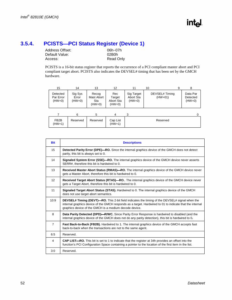
Intel® 82810E (GMCH)
R
52 Datasheet
3.5.4. PCISTSPCI Status Register (Device 1) Address Offset: 06h−07h Default Value: 02B0h Access: Read Only
PCISTS is a 16-bit status register that reports the occurrence of a PCI compliant master abort and PCI compliant target abort. PCISTS also indicates the DEVSEL# timing that has been set by the GMCH hardware.
15 14 13 12 11 10 9 8
Detected Par Error (HW=0)
Sig Sys Error
(HW=0)
Recog Mast Abort
Sta (HW=0)
Rec Target
Abort Sta (HW=0)
Sig Target Abort Sta (HW=0)
DEVSEL# Timing (HW=01)
Data Par Detected (HW=0)
7 6 5 4 3 0
FB2B (HW=1)
Reserved Reserved Cap List (HW=1)
Reserved
Bit Descriptions
15 Detected Parity Error (DPE)RO. Since the internal graphics device of the GMCH does not detect parity, this bit is always set to 0.
14 Signaled System Error (SSE)RO. The internal graphics device of the GMCH device never asserts SERR#, therefore this bit is hardwired to 0.
13 Received Master Abort Status (RMAS)RO. The internal graphics device of the GMCH device never gets a Master Abort, therefore this bit is hardwired to 0.
12 Received Target Abort Status (RTAS)RO.. The internal graphics device of the GMCH device never gets a Target Abort, therefore this bit is hardwired to 0.
11 Signaled Target Abort Status (STAS). Hardwired to 0. The internal graphics device of the GMCH does not use target abort semantics.
10:9 DEVSEL# Timing (DEVT)RO. This 2-bit field indicates the timing of the DEVSEL# signal when the internal graphics device of the GMCH responds as a target. Hardwired to 01 to indicate that the internal graphics device of the GMCH is a medium decode device.
8 Data Parity Detected (DPD)R/WC. Since Parity Error Response is hardwired to disabled (and the internal graphics device of the GMCH does not do any parity detection), this bit is hardwired to 0.
7 Fast Back-to-Back (FB2B). Hardwired to 1. The internal graphics device of the GMCH accepts fast back-to-back when the transactions are not to the same agent.
6:5 Reserved.
4 CAP LISTRO. This bit is set to 1 to indicate that the register at 34h provides an offset into the function’s PCI Configuration Space containing a pointer to the location of the first item in the list.
3:0 Reserved.
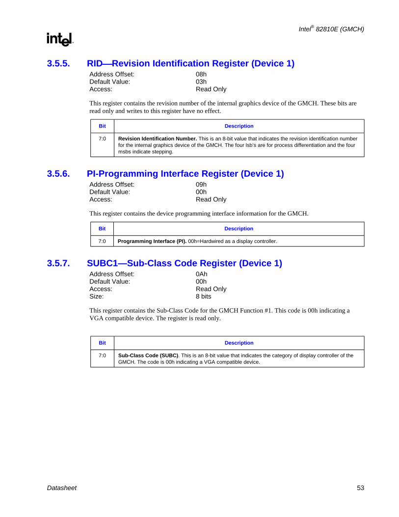
Intel® 82810E (GMCH)
R
Datasheet 53
3.5.5. RIDRevision Identification Register (Device 1) Address Offset: 08h Default Value: 03h Access: Read Only
This register contains the revision number of the internal graphics device of the GMCH. These bits are read only and writes to this register have no effect.
Bit Description
7:0 Revision Identification Number. This is an 8-bit value that indicates the revision identification number for the internal graphics device of the GMCH. The four lsb’s are for process differentiation and the four msbs indicate stepping.
3.5.6. PI-Programming Interface Register (Device 1) Address Offset: 09h Default Value: 00h Access: Read Only
This register contains the device programming interface information for the GMCH.
Bit Description
7:0 Programming Interface (PI). 00h=Hardwired as a display controller.
3.5.7. SUBC1—Sub-Class Code Register (Device 1) Address Offset: 0Ah Default Value: 00h Access: Read Only Size: 8 bits
This register contains the Sub-Class Code for the GMCH Function #1. This code is 00h indicating a VGA compatible device. The register is read only.
Bit Description
7:0 Sub-Class Code (SUBC). This is an 8-bit value that indicates the category of display controller of the GMCH. The code is 00h indicating a VGA compatible device.

Intel® 82810E (GMCH)
R
54 Datasheet
3.5.8. BCC1—Base Class Code Register (Device 1) Address Offset: 0Bh Default Value: 03h Access: Read Only Size: 8 bits
This register contains the Base Class Code of the GMCH Function #1.
Bit Description
7:0 Base Class Code (BASEC). This is an 8-bit value that indicates the Base Class Code for the GMCH. This code has the value 03h, indicating a display controller.
3.5.9. CLSCache Line Size Register (Device 1) Address Offset: 0Ch Default Value: 00h Access: Read only
The internal graphics device of the GMCH does not support this register as a PCI slave.
Bit Description
7:0 Cache Line Size (CLS). Hardwired to 0’s. The internal graphics device of the GMCH as a PCI compliant master does not use the Memory Write and Invalidate command and, in general, does not perform operations based on cache line size.
3.5.10. MLTMaster Latency Timer Register (Device 1) Address Offset: 0Dh Default Value: 00h Access: Read Only
The internal graphics device of the GMCH does not support the programmability of the master latency timer because it does not perform bursts.
Bit Description
7:0 Master Latency Timer Count Value. Hardwired to 0s.

Intel® 82810E (GMCH)
R
Datasheet 55
3.5.11. HDRHeader Type Register (Device 1) Address Offset: 0Eh Default Value: 00h Access: Read Only
This register contains the Header Type of the internal graphics device of the GMCH.
Bit Description
7:0 Header Type (HTYPE). This is an 8-bit value that indicates the Header Type for the internal graphics device of the GMCH. This code has the value 00h, indicating a basic (i.e., single function) configuration space format.
3.5.12. BISTBuilt In Self Test (BIST) Register (Device 1) Address Offset: 0Fh Default Value: 00h Access: Read Only
This register is used for control and status of Built In Self Test (BIST) for the internal graphics device of the GMCH.
7 6 0
BIST Supported (HW=0)
Reserved
Bit Descriptions
7 BIST Supported. BIST is not supported. This bit is hardwired to 0.
6:0 Reserved

Intel® 82810E (GMCH)
R
56 Datasheet
3.5.13. GMADRGraphics Memory Range Address Register (Device 1) Address Offset: 10−13h Default Value: 00000008h Access: Read/Write, Read Only
This register requests allocation for the internal graphics device of the GMCH local memory. The allocation is for either 32 MB or 64 MB of memory space (selected by bit 0 of the Device 0 MISCC Register) and the base address is defined by bits [31:25,24].
31 26 25 24 16
Memory Base Address (addr bits [31:26])
64 MB Addr Mask
Address Mask (HW=0; 32MB addr range)
15 4 3 2 1 0
Address Mask (cont) (HW=0; 32MB addr range)
Prefetch Mem En (HW=1)
Memory Type (HW=0; 32MB addr)
Mem/IO Space
(HW=0)
Bit Descriptions
31:26 Memory Base AddressR/W. Set by the OS, these bits correspond to address signals [31:26].
25 64M Address Mask—RO , R/W. If Device 0 MISCC Reg bit 0 = 0 then this bit is Read Only with a value of “0”, indicating a memory range of 64MB, if Device 0 MISCC Reg bit 0 = 1 then this bit is R/W, indicating a memory range of 32 MB.
24:4 Address MaskRO. Hardwired to 0s to indicate 32 MB address range.
3 Prefetchable MemoryRO. Hardwired to 1 to enable prefetching.
2:1 Memory TypeRO. Hardwired to 0 to indicate 32-bit address.
0 Memory/IO SpaceRO. Hardwired to 0 to indicate memory space.
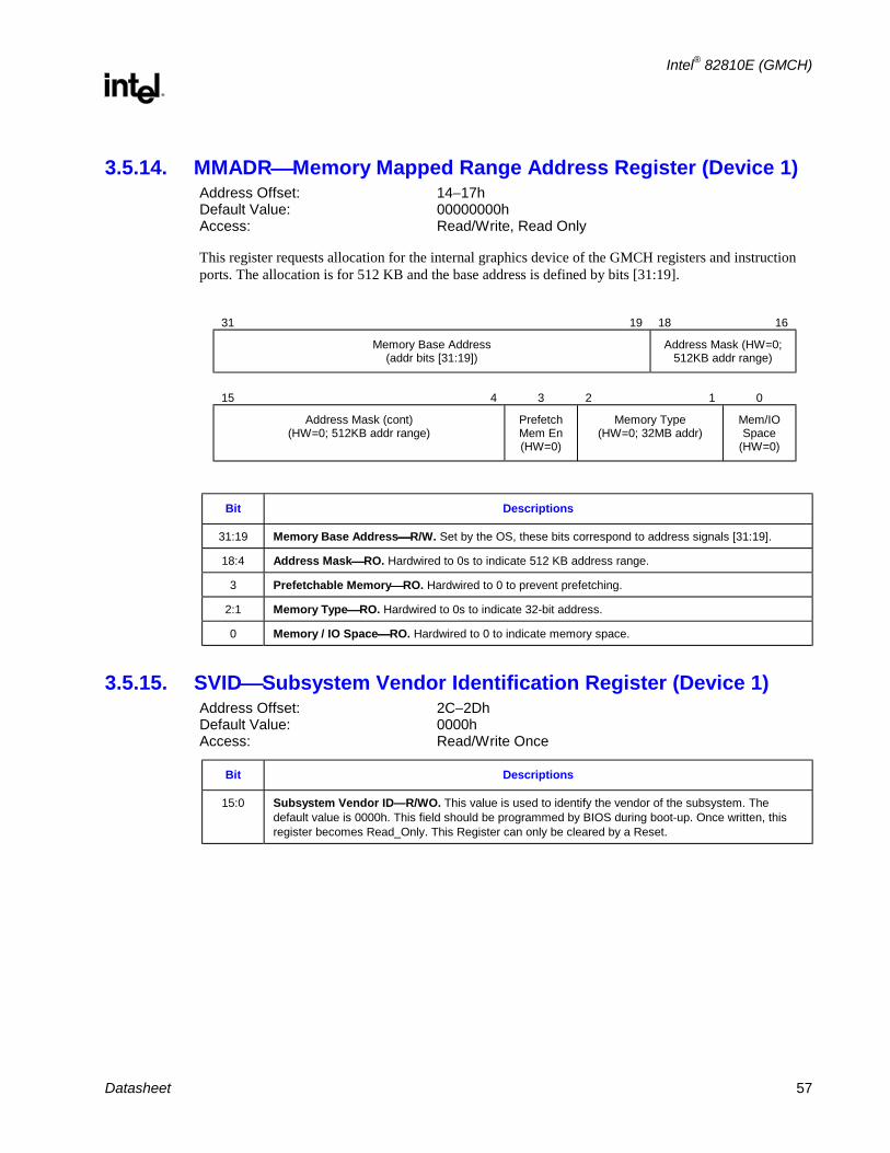
Intel® 82810E (GMCH)
R
Datasheet 57
3.5.14. MMADRMemory Mapped Range Address Register (Device 1) Address Offset: 14−17h Default Value: 00000000h Access: Read/Write, Read Only
This register requests allocation for the internal graphics device of the GMCH registers and instruction ports. The allocation is for 512 KB and the base address is defined by bits [31:19].
31 19 18 16
Memory Base Address (addr bits [31:19])
Address Mask (HW=0; 512KB addr range)
15 4 3 2 1 0
Address Mask (cont) (HW=0; 512KB addr range)
Prefetch Mem En (HW=0)
Memory Type (HW=0; 32MB addr)
Mem/IO Space
(HW=0)
Bit Descriptions
31:19 Memory Base AddressR/W. Set by the OS, these bits correspond to address signals [31:19].
18:4 Address MaskRO. Hardwired to 0s to indicate 512 KB address range.
3 Prefetchable MemoryRO. Hardwired to 0 to prevent prefetching.
2:1 Memory TypeRO. Hardwired to 0s to indicate 32-bit address.
0 Memory / IO SpaceRO. Hardwired to 0 to indicate memory space.
3.5.15. SVIDSubsystem Vendor Identification Register (Device 1) Address Offset: 2C−2Dh Default Value: 0000h Access: Read/Write Once
Bit Descriptions
15:0 Subsystem Vendor ID—R/WO. This value is used to identify the vendor of the subsystem. The default value is 0000h. This field should be programmed by BIOS during boot-up. Once written, this register becomes Read_Only. This Register can only be cleared by a Reset.

Intel® 82810E (GMCH)
R
58 Datasheet
3.5.16. SIDSubsystem Identification Register (Device 1) Address Offset: 2E−2Fh Default Value: 0000h Access: Read/Write Once
Bit Descriptions
15:0 Subsystem ID—R/WO. This value is used to identify a particular subsystem. The default value is 0000h. This field should be programmed by BIOS during boot-up. Once written, this register becomes Read_Only. This Register can only be cleared by a Reset.
3.5.17. ROMADRVideo BIOS ROM Base Address Registers (Device 1) Address Offset: 30−33h Default Value: 00000000h Access: Read Only
The internal graphics device of the GMCH does not use a separate BIOS ROM, therefore this is hardwired to 0s.
31 18 17 16
ROM Base Address (addr bits [31:19])
Address Mask (HW=0; 256KB addr range)
15 11 10 1 0
Address Mask (cont) (HW=0; 256KB addr range)
Reserved (HW=0) ROM BIOS En (HW=0)
Bit Descriptions
31:18 ROM Base AddressRO. Hardwired to 0s.
17:11 Address MaskRO. Hardwired to 0s to indicate 256 KB address range.
10:1 Reserved. Hardwired to 0s.
0 ROM BIOS EnableRO. 0 = ROM not accessible.
3.5.18. CAPPOINTCapabilities Pointer Register (Device 1) Address Offset: 34h Default Value: DCh Access: Read Only
Bit Descriptions
7:0 Pointer to the Atart of AGP Register Block. Since there is no AGP bus on the GMCH, this field is set to DCh to point to the Power Management Capabilities ID Register
Intel® 82810E (GMCH)
R
Datasheet 59
3.5.19. INTRLINEInterrupt Line Register (Device 1) Address Offset: 3Ch Default Value: 00h Access: Read/Write
Bit Descriptions
7:0 Interrupt Connection. Used to communicate interrupt line routing information. POST software writes the routing information into this register as it initializes and configures the system. The value in this register indicates which input of the system interrupt controller that the device’s interrupt pin is connected to.
3.5.20. INTRPINInterrupt Pin Register (Device 1) Address Offset: 3Dh Default Value: 01h Access: Read Only
Bit Descriptions
7:0 Interrupt Pin. As a single function device, GMCH specifies INTA# as its interrupt pin.
01h=INTA#.
3.5.21. MINGNTMinimum Grant Register (Device 1) Address Offset: 3Eh Default Value: 00h Access: Read Only
Bit Descriptions
7:0 Minimum Grant Value. GMCH does not burst as a PCI compliant master.
Bits[7:0]=00h.
3.5.22. MAXLATMaximum Latency Register (Device 1) Address Offset: 3Fh Default Value: 00h Access: Read Only
Bit Descriptions
7:0 Maximum Latency Value. Bits[7:0]=00h. The GMCH has no specific requirements for how often it needs to access the PCI bus.
Intel® 82810E (GMCH)
R
60 Datasheet
3.5.23. PM_CAPIDPower Management Capabilities ID Register (Device 1) Address Offset: DCh−DDh Default Value: 0001h Access: Read Only
15 8 7 0
NEXT_PTR CAP_ID
Bits Description
15:8 NEXT_PTR. This contains a pointer to next item in capabilities list. This the final capability in the list and must be set to 00h.
7:0 CAP_ID. SIG defines this ID is 01h for power management.
3.5.24. PM_CAPPower Management Capabilities Register (Device 1) Address Offset: DEh−DFh Default Value: 0021h Access: Read Only
15 11 10 9 8
PME Support (HW=0) D2 (HW=0)
D1 (HW=0)
Reserved
7 6 5 4 3 2 0
Reserved Dev Specific
Init (HW=1)
Aux Pwr Src
(HW=0)
PME Clock
(HW=0)
Version (HW=001)
Bits Description
15:11 PME Support. This field indicates the power states in which the GMCH may assert PME#. Hardwired to 0 to indicate that the GMCH does not assert the PME# signal.
10 D2. Hardwired to 0 to indicate D2 power management state is not supported.
9 D1. Hardwired to 0 to indicate that D1 power management state is not supported.
8:6 Reserved. Read as 0s.
5 Device Specific Initialization (DSI). Hardwired to 1 to indicate that special initialization of the GMCH is required before generic class device driver is to use it.
4 Auxiliary Power Source. Hardwired to 0.
3 PME Clock. Hardwired to 0 to indicate the GMCH does not support PME# generation.
2:0 Version. Hardwired to 001b to indicate there are 4 bytes of power management registers implemented.
Intel® 82810E (GMCH)
R
Datasheet 61
3.5.25. PM_CS—Power Management Control/Status Register (Device 1) Address Offset: E0h−E1h Default Value: 0000h Access: Read/Write
15 14 13 12 9 8
PME Sta (HW=0)
Data Scale (Reserved) Data_Select (Reserved) PME En
7 2 1 0
Reserved PowerState
Bits Description
15 PME_Status R/WC. This bit is 0 to indicate that the GMCH does not support PME# generation from D3 (cold).
14:13 Data Scale (Reserved) RO. The GMCH does not support data register. This bit always returns 0 when read, write operations have no effect.
12:9 Data_Select (Reserved) RO. The GMCH does not support data register. This bit always returns 0 when read, write operations have no effect.
8 PME_EnR/W. This bit is 0 to indicate that PME# assertion from D3 (cold) is disabled.
7:2 Reserved. Always returns 0 when read, write operations have no effect.
1:0 PowerStateR/W. This field indicates the current power state of the GMCH and can be used to set the GMCH into a new power state. If software attempts to write an unsupported state to this field, write operation must complete normally on the bus, but the data is discarded and no state change occurs.
00 = D0
01 = Reserved
10 = Reserved
11 = D3
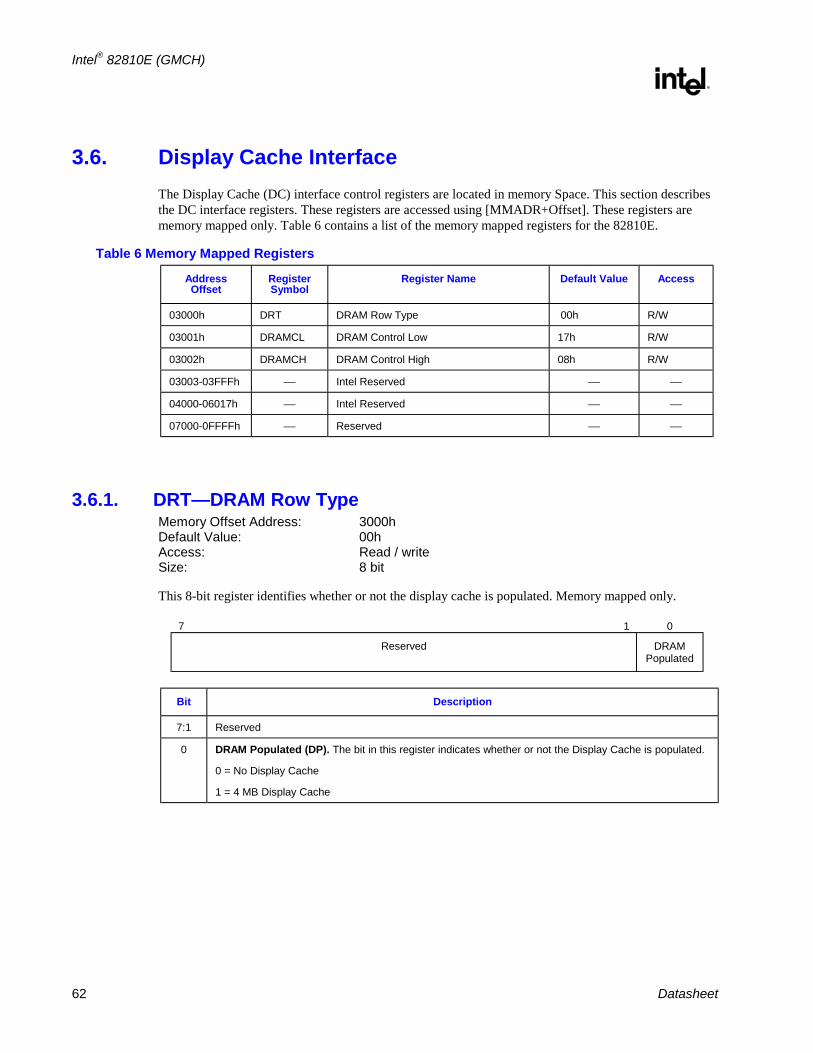
Intel® 82810E (GMCH)
R
62 Datasheet
3.6. Display Cache Interface The Display Cache (DC) interface control registers are located in memory Space. This section describes the DC interface registers. These registers are accessed using [MMADR+Offset]. These registers are memory mapped only. Table 6 contains a list of the memory mapped registers for the 82810E.
Table 6 Memory Mapped Registers
Address Offset
Register Symbol
Register Name Default Value Access
03000h DRT DRAM Row Type 00h R/W
03001h DRAMCL DRAM Control Low 17h R/W
03002h DRAMCH DRAM Control High 08h R/W
03003-03FFFh Intel Reserved
04000-06017h Intel Reserved
07000-0FFFFh Reserved
3.6.1. DRT—DRAM Row Type Memory Offset Address: 3000h Default Value: 00h Access: Read / write Size: 8 bit
This 8-bit register identifies whether or not the display cache is populated. Memory mapped only.
7 1 0
Reserved DRAM Populated
Bit Description
7:1 Reserved
0 DRAM Populated (DP). The bit in this register indicates whether or not the Display Cache is populated.
0 = No Display Cache
1 = 4 MB Display Cache

Intel® 82810E (GMCH)
R
Datasheet 63
3.6.2. DRAMCL—DRAM Control Low Memory Offset Address: 3001h Default Value: 17h Access: Read / write Size : 8 bit
7 5 4 3 2 1 0
Reserved Paging Mode
Control
RAS-to-CAS
Override
CAS# Latency
RAS# Riming
RAS# Precharge
Timing
Bit Description
7:5 Reserved
4 Paging Mode Control (PMC).
0 = Page Open Mode. In this mode the GMCH memory controller tends to leave pages open.
1 = Page Close Mode. In this mode the GMCH memory controller tends to leave pages closed.
3 RAS-to-CAS Override (RCO). In units of display cache clock periods indicates the RAS#-to-CAS# delay (tRCD). (i.e., row activate command to read/write command)
0 = Determined by CL bit (default)
1 = 2
2 CAS# Latency (CL). In units of local memory clock periods.
Bit CL RAS#-to-CAS# delay (tRCD)
0 2 2
1 3 3 (default)
1 RAS# Timing (RT). This bit controls RAS# active to precharge, and refresh to RAS# active delay (in local memory clocks).
Bit RAS# act. To precharge (tRAS) Refresh to RAS# act. (tRC)
0 5 8
1 7 10 (default)
0 RAS# Precharge Timing (RPT). This bit controls RAS# precharge (in local memory clocks).
0 = 2
1 = 3 (default)

Intel® 82810E (GMCH)
R
64 Datasheet
3.6.3. DRAMCH—DRAM Control High Memory Offset Address: 3002h Default Value: 08h Access: Read / write Size: 8 bit
7 5 4 3 2 0
Reserved DRAM Refresh Rate Special Mode Select
Bit Description
7:5 Reserved
4:3 DRAM Refresh Rate (DRR). DRAM refresh is controlled using this field. Disabling refresh results in the eventual loss of DRAM data, although refresh can be briefly disabled without data loss. The field must be set to normal refresh as soon as possible once DRAM testing is completed.
00 = Refresh Disabled
01 = Refresh Enabled (default)
10 = Reserved
11 = Reserved
2:0 Special Mode Select (SMS). These bits select special SDRAM modes used for testing and initialization. The NOP command must be programmed first before any other command can be issued.
000 = Normal SDRAM mode (Normal, default).
001 = NOP Command Enable (NCE). This state forces cycles to DRAM to generate SDRAM NOP commands.
010 = All Banks Precharge Command Enable (ABPCE). This state forces cycles to DRAM to generate an all banks precharge command.
011 = Mode Register Command Enable (MRCE). This state forces all cycles to DRAM to be converted into MRS commands. The command is driven on the LMA[11:0] lines. LMA[2:0] correspond to the burst length, LMA[3] corresponds to the wrap type, and LMA[6:4] correspond to the latency mode. LMA[11:7] are driven to 00000 by the GMCH,
The BIOS must select an appropriate host address for each row of memory such that the right commands are generated on the LMA[6:0] lines, taking into account the mapping of host addresses to display cache addresses.
100 = CBR Cycle Enable (CBRCE). This state forces cycles to DRAM to generate SDRAM CBR refresh cycles.
101 = Reserved.
11X = Reserved.
Intel® 82810E (GMCH)
R
Datasheet 65
3.7. Display Cache Detect and Diagnostic Registers The following registers are used for display cache detection and diagnostics. These registers can be accessed via either I/O space or memory space. The memory space addresses listed are offsets from the base memory address programmed into the MMADR register (Device 1, PCI configuration offset 14h). For each register, the memory-mapped address offset is the same address value as the I/O address. See the Intel® 810E chipset BIOS specification for the proper setting of these registers for display cache detection and diagnostics.
3.7.1. GRXGRX Graphics Controller Index Register I/O (and Memory Offset) Address: 3CEh Default: 0Uh (U=Undefined) Attributes: Read/Write
7 4 3 0
Reserved (0000) Graphics Controller Register Index
Bit Description
7:4 Reserved. Read as 0s.
3:0 Sequencer Register Index. This field selects any one of the graphics controller registers (GR[00:08) to be accessed via the data port at I/O location 3CFh.

Intel® 82810E (GMCH)
R
66 Datasheet
3.7.2. MSRMiscellaneous Output I/O (and Memory Offset) Address: 3C2h Write; 3CCh Read Default: 00h Attributes: See Address above
7 2 1 0
Reserved A0000h− BFFFFh Acc En
Reserved
Bit Descriptions
7:2 Reserved
1 A0000−−−−BFFFFh Access Enable. VGA Compatibility bit enables access to the display cache at A0000h−BFFFFh. When disabled, accesses to system memory are blocked in this region (by not asserting DEVSEL#). This bit does not block processor access to the video linear frame buffer at other addresses.
0 = Prevent processor access to the display cache (default).
1 = Allow processor access to display cache.
0 Reserved

Intel® 82810E (GMCH)
R
Datasheet 67
3.7.3. GR06Miscellaneous Register I/O (and Memory Offset) Address: 3CFh (Index=06h) Default: 0Uh (U=Undefined) Attributes: Read/Write
7 4 3 2 1 0
Reserved Memory Map Mode Reserved
Bit Description
7:4 Reserved
3:2 Memory Map Mode. These 2 bits control the mapping of the VGA frame buffer into the processor address space as follows:
00 = A0000h – BFFFFh
01 = A0000h − AFFFFh
10 = B0000h − B7FFFh
11 = B8000h − BFFFFh
Note: This function is both in standard VGA modes and in extended modes that do not provide linear frame buffer accesses.
1:0 Reserved
Intel® 82810E (GMCH)
R
68 Datasheet
3.7.4. GR10Address Mapping I/O (and Memory Offset) Address: 3CFh (Index=10h) Default: 00h Attributes: R/W
7 5 4 3 2 1 0
Reserved Paging to display cache
VGA Buffer
/Memory Map
Packed Mode Enbl
Linear Mapping
Page Mapping
Bit Description
7:5 Reserved
4 Page to Display Cache Enable.
0 = Page to VGA Buffer.
1 = Page to Display Cache.
3 VGA Buffer/Memory Map Select.
0 = VGA Buffer (default)
1 = Memory Map.
2 Packed Mode Enable.
0 = Disable (default)
1 = Enable
1 Linear Mapping (PCI).
0 = Disable (default)
1 = Enable
0 Page Mapping Enable. This mode allows the mapping of the vga space allocated in main memory (non local video memory) mode or all of local memory space through the A0000:AFFFF window that is a 64 KB page.
0 = Disable (default)
1 = Enable
3.7.5. GR11Page Selector I/O (and Memory Offset) Address: 3CFh (Index=11h) Default : 00h Attributes: R/W
Bit Description
7:0 Page Select. Selects a 64 KB window within the display cache when Page Mapping is enabled to the display cache.
Intel® 82810E (GMCH)
R
Datasheet 69
4. Functional Description This chapter describes the Graphics and Memory Controller Hub (GMCH) interfaces on-chip functional units. Sectiom 4.1, “System Address Map”, provides a system-level address memory map and describes the memory space controls provided by the GMCH.
4.1. System Address Map An Intel Pentium® III processor, Intel Pentium® II processor, or Intel CeleronTM processor system based on the GMCH, supports 4 GB of addressable memory space and 64 KB+3 of addressable I/O space. (The P6 bus I/O addressability is 64KB + 3). There is a programmable memory address space under the 1 MB region that can be controlled with programmable attributes of Write Only, or Read Only. Attribute programming is described in Chapter 3, “Configuration Registers”. This section focuses on how the memory space is partitioned and what these separate memory regions are used for. The I/O address space is explained at the end of this section.
The Intel Pentium III processor, Intel Pentium II processor, and Intel CeleronTM processor supports addressing of memory ranges larger than 4 GB. The GMCH Host Bridge claims any access over 4 GB by terminating transaction (without forwarding it to the hub interface). Writes are terminated by dropping the data and for reads the GMCH returns all zeros on the host bus.
In the following sections, it is assumed that all of the compatibility memory ranges reside on the hub interface. The exceptions to this rule are the VGA ranges that may be mapped to the internal Graphics Device.
Note: The GMCH Memory Map includes a number of programmable ranges, ALL of these ranges MUST be unique and NON-OVERLAPPING. There are NO Hardware Interlocks to prevent problems in the case of overlapping ranges. Accesses to overlapped ranges may produce indeterminate results.

Intel® 82810E (GMCH)
R
70 Datasheet
4.1.1. Memory Address Ranges
Figure 3 shows a high-level representation of the system memory address map. Figure 4 provides additional details on mapping specific memory regions as defined and supported by the GMCH chipset.
Figure 3. System Memory Address Map
Top of the Main Memory
PCIMemoryAddressRange
4 GB
0
IndependentlyProgrammable Non-Overlapping Memory
Windows
mem_map_s.vsd
Local
Memory
Range
Memory
Mapped
Range
MainMemoryAddressRange

Intel® 82810E (GMCH)
R
Datasheet 71
Figure 4. Detailed Memory System Address Map
mem_map2.vsd
DOS Area(640 KB)
000000h
0A0000h09FFFFh
0C0000h0BFFFFh
0D0000h0CFFFFh
0E0000h0DFFFFh
0FFFFFh 1 MB
896 KB
832 KB
768 KB
640 KB
0 KB
0F0000h0EFFFFh 960 KB
0DC000h0DBFFFh
880 KB
MainMemory
00000h
A0000h9FFFFh
BFFFFh
System/Application SW
Graphics Adapter(128 KB)
C0000hVideo BIOS
(shadowed in memory)
100000h0FFFFFh
DOSCompatibility
Memory
1 MB
Optionallymapped to the
internal GC
Std PCI/ISA Video Mem(SMM Mem) 128 KB
Segment C(BIOS Shadow Area, etc.)
Segment D(BIOS Shadow Area, etc.)
Optional CD Hole
Segment E(BIOS Shadow Area, etc.)
Segment F(BIOS Shadow Area, etc.)
4 GB
System Memory Space
Graphics (virtual)Memory
(32MB/64MB)
Size=32/64MB; MISCC Reg.(72h); Dev 0
Base=MMADR Reg.(14h); Dev 1
64 GB
Extended CPUMemory Space
PCI Memory Accesses toGraphics (Virtual) Memory
PCI Memory accessesto GC registers
PCI Memory
PCI Memory
Graphics Controller (GC)(memory-mapped
control/status registers)
PCI Memory
Optional TSEGSize=0KB/512KB/1MB;SMRAM Reg. (70h); Dev 0
TOM (512 MB Max.)
PCI Memory
Optional HSEGFEEA 0000hFEE9 FFFFh
FEEC 0000hFEEB FFFFh
Base=GMADR Reg.(10h); Dev 1
Size=512 KB – fixed
Optional GraphicsDevice
Optional ISA Hole15 MB
16 MB
Size=0KB/512KB/1MB;SMRAM Reg. (70h); Dev 0
4.1.1.1. Compatibility Area
This area is divided into the following address regions:
• 0–640 KB DOS Area
• 640–768 KB Video Buffer Area
• 768 KB–1 MB Memory (BIOS Area). System BIOS area, Extended System BIOS area, and Expansion area
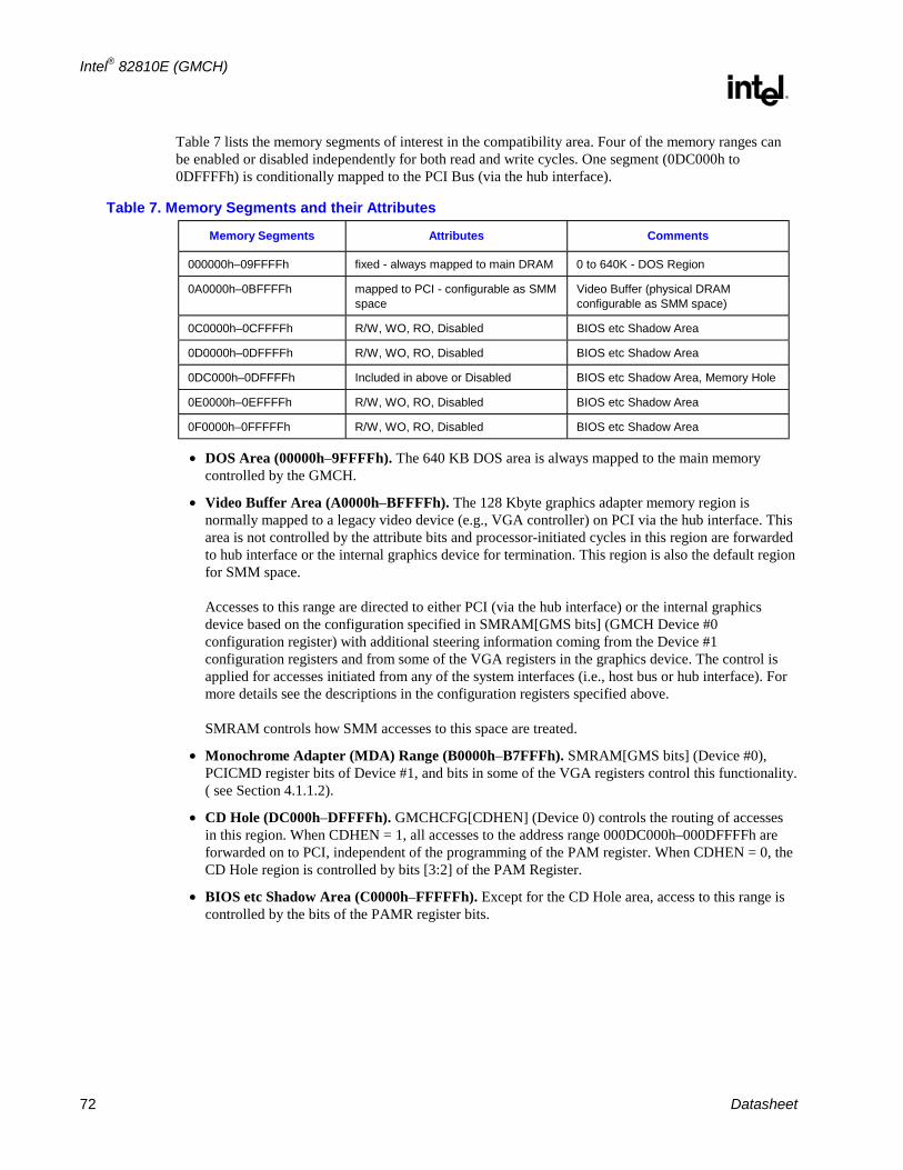
Intel® 82810E (GMCH)
R
72 Datasheet
Table 7 lists the memory segments of interest in the compatibility area. Four of the memory ranges can be enabled or disabled independently for both read and write cycles. One segment (0DC000h to 0DFFFFh) is conditionally mapped to the PCI Bus (via the hub interface).
Table 7. Memory Segments and their Attributes
Memory Segments Attributes Comments
000000h–09FFFFh fixed - always mapped to main DRAM 0 to 640K - DOS Region
0A0000h–0BFFFFh mapped to PCI - configurable as SMM space
Video Buffer (physical DRAM configurable as SMM space)
0C0000h–0CFFFFh R/W, WO, RO, Disabled BIOS etc Shadow Area
0D0000h–0DFFFFh R/W, WO, RO, Disabled BIOS etc Shadow Area
0DC000h–0DFFFFh Included in above or Disabled BIOS etc Shadow Area, Memory Hole
0E0000h–0EFFFFh R/W, WO, RO, Disabled BIOS etc Shadow Area
0F0000h–0FFFFFh R/W, WO, RO, Disabled BIOS etc Shadow Area
• DOS Area (00000h–9FFFFh). The 640 KB DOS area is always mapped to the main memory controlled by the GMCH.
• Video Buffer Area (A0000h–BFFFFh). The 128 Kbyte graphics adapter memory region is normally mapped to a legacy video device (e.g., VGA controller) on PCI via the hub interface. This area is not controlled by the attribute bits and processor-initiated cycles in this region are forwarded to hub interface or the internal graphics device for termination. This region is also the default region for SMM space. Accesses to this range are directed to either PCI (via the hub interface) or the internal graphics device based on the configuration specified in SMRAM[GMS bits] (GMCH Device #0 configuration register) with additional steering information coming from the Device #1 configuration registers and from some of the VGA registers in the graphics device. The control is applied for accesses initiated from any of the system interfaces (i.e., host bus or hub interface). For more details see the descriptions in the configuration registers specified above. SMRAM controls how SMM accesses to this space are treated.
• Monochrome Adapter (MDA) Range (B0000h–B7FFFh). SMRAM[GMS bits] (Device #0), PCICMD register bits of Device #1, and bits in some of the VGA registers control this functionality. ( see Section 4.1.1.2).
• CD Hole (DC000h–DFFFFh). GMCHCFG[CDHEN] (Device 0) controls the routing of accesses in this region. When CDHEN = 1, all accesses to the address range 000DC000h–000DFFFFh are forwarded on to PCI, independent of the programming of the PAM register. When CDHEN = 0, the CD Hole region is controlled by bits [3:2] of the PAM Register.
• BIOS etc Shadow Area (C0000h–FFFFFh). Except for the CD Hole area, access to this range is controlled by the bits of the PAMR register bits.
Intel® 82810E (GMCH)
R
Datasheet 73
4.1.1.2. Extended Memory Area
This memory area covers the 100000h (1 MB) to FFFFFFFFh (4 GB-1) address range and it is divided into regions as specified in the following sections.
Main DRAM Address Region (0010_0000h to Top of Main Memory)
The address range from 1 MB to the top of main memory is mapped to main the DRAM address range controlled by the GMCH. All accesses to addresses within this range, except those listed below, are forwarded by the GMCH to DRAM.
• Optional ISA Memory Hole (15 MB–16 MB). A 1 MB ISA memory hole in the main DRAM range can be enabled via the FDHC register (Device 0). Note that this memory is not re-mapped. Accesses to this range are forwarded to PCI (via the hub interface)
• TSEG. This Extended SMRAM Address Range, if enabled, occupies the 512 KB or 1 MB range below the Top of Main Memory. The size of TSEG is determined by SMRAM[USMM] (Device 0). When the extended SMRAM space is enabled, non-SMM processor accesses and all other accesses in this range are forwarded to PCI (via the hub interface). When SMM is enabled, the amount of memory available to the system is reduced by the TSEG range.
• Optional Graphics Device Memory. This address range provides either 512KB or 1MB of VGA buffer memory for the internal graphics device . If TSEG is enabled, this address range is just below TSEG. If TSEG is not enabled, the Optional Graphics Device VGA buffer range is just below TOM. The Graphics Device buffer memory range is enabled and the size selected via SMRAM[GMS].
PCI Memory Address Region (Top of Main Memory to 4 GB)
The address range from the top of main DRAM to 4 GB (top of physical memory space supported by the GMCH) is normally mapped to PCI (via the hub interface), except for the address ranges listed below.
There are two sub-ranges within the PCI Memory address range defined as APIC Configuration Space and High BIOS Address Range. The Local Memory Range and the Memory Mapped Range of the internal Graphics Device MUST NOT overlap with these two ranges.
• GMCH’s Graphics Controller Status/Control Register Range. A 512 KB space for the graphics controller device’s memory-mapped status/control registers that is requested during Plug and Play. The base address is programmed in the MMADR PCI Configuration Register for Device 1. Note that, for legacy support, the VGA registers in the GMCH’s graphics controller are also mapped to the normal I/O locations.

Intel® 82810E (GMCH)
R
74 Datasheet
Figure 5 GMCH’s Graphics Register Memory Address Space
reginstm.vsd
Intel Reserved
Display Cache InterfaceControl Registers
00000h
00FFFh01000h
VGA and Ext. VGA RegistersVGA and Ext. VGA Registers
I/O Space Map(Standard graphics locations)
Memory Space Map(512 KB allocation)
Offset FromBase_Reg
Intel Reserved04FFFh05000h
02FFFh03000h
03FFFh04000h
05FFFh06000h
06FFFh07000h
0FFFFh10000h
Intel Reserved
Intel Reserved
1FFFFh20000h
2FFFFh30000h
3FFFFh40000h
4FFFFh50000h
5FFFFh
70000h
7FFFFh
Intel Reserved
Intel Reserved
Intel Reserved
Intel Reserved
Intel Reserved
60000h
6FFFFh
Intel Reserved
MMADR Register(Base Address)
1931
• Graphics Controller Graphics Memory Range. The GMCH’s graphics controller device uses a logical memory concept to access graphics memory. The logical graphics memory size is programmable as either 32 MB or 64 MB and is allocated by BIOS during Plug and Play. This address range is programmed in the GMADR Register (Device 1) and the MISCC Register (Device 0). The graphics controller engines can access this address space of which the lower 32 MB or all 64 MB correspond to graphics memory accessable by the processor.
Intel® 82810E (GMCH)
R
Datasheet 75
• APIC Configuration Space (FEC0_0000h–FECF_FFFFh, FEE0_0000h–FEEF_FFFFh). This range is reserved for APIC configuration space that includes the default I/O APIC configuration space. The default Local APIC configuration space is FEE0_0000h to FEEF_0FFFh. Processor accesses to the Local APIC configuration space do not result in external bus activity since the Local APIC configuration space is internal to the processor. However, a MTRR must be programmed to make the Local APIC range uncacheable (UC). The Local APIC base address in each processor should be relocated to the FEC0_0000h (4GB–20MB) to FECF_FFFFh range so that one MTRR can be programmed to 64 KB for the Local and I/O APICs. The I/O APIC(s) usually reside in the I/O Bridge portion of the chipset or as a stand-alone component(s). I/O APIC units will be located beginning at the default address FEC0_0000h. The first I/O APIC is located at FEC0_0000h. Each I/O APIC unit is located at FEC0_x000h where x is I/O APIC unit number 0 through F(hex). This address range will be normally mapped via hub interface to PCI. The address range between the APIC configuration space and the High BIOS (FED0_0000h to FEDF_FFFFh) is always mapped to PCI (via the hub interface).
• High BIOS Area (FFE0_0000h–FFFF_FFFFh). The top 2 MB of the Extended Memory Region is reserved for System BIOS (High BIOS), extended BIOS for PCI devices, and the A20 alias of the system BIOS. Processor begins execution from the High BIOS after reset. This region is mapped to PCI (via the hub interface) so that the upper subset of this region aliases to 16 MB–256 KB range. The actual address space required for the BIOS is less than 2 MB but the minimum processor MTRR range for this region is 2 MB so that full 2 MB must be considered. The ICH supports a maximum of 1 MB in the High BIOS range.
• Optional HSEG. This Extended SMRAM Address Range, if enabled via the SMRAM register, occupies the range from FEEA_0000h to FEEB_FFFFh. Maps to A0000h–BFFFFh when enabled.
4.1.1.3. System Management Mode (SMM) Memory Range
The GMCH supports the use of main memory as System Management RAM (SMRAM), enabling the use of System Management Mode. The GMCH supports two SMRAM options: Compatible SMRAM (C_SMRAM) and Extended SMRAM (E_SMRAM). System Management RAM (SMRAM) space provides a memory area that is available for the SMI handler's and code and data storage. This memory resource is normally hidden from the system OS so that the processor has immediate access to this memory space upon entry to SMM. The GMCH provides three SMRAM options:
• Below 1 MB option that supports compatible SMI handlers.
• Above 1 MB option that allows new SMI handlers to execute with write-back cacheable SMRAM.
• Optional larger write-back cacheable T_SEG area of either 512 KB or 1MB in size above 1 MB that is reserved from the highest area in system DRAM memory. The above 1 MB solutions require changes to compatible SMRAM handlers code to properly execute above 1 MB.
Refer to the Power Management section for more details on SMRAM support.
Intel® 82810E (GMCH)
R
76 Datasheet
4.1.2. Memory Shadowing
Any block of memory that can be designated as read-only or write-only can be “shadowed” into the GMCH DRAM memory. Typically this is done to allow ROM code to execute more rapidly out of main DRAM. ROM is used as a read-only during the copy process while DRAM at the same time is designated write-only. After copying, the DRAM is designated read-only so that ROM is shadowed. Processor bus transactions are routed accordingly.
4.1.3. I/O Address Space
The GMCH does not support the existence of any other I/O devices besides itself on the processor bus. The GMCH generates hub interface bus cycles for all processor I/O accesses that do not target the Legacy I/O registers supported by the internal Graphics Device. The GMCH contains two internal registers in the processor I/O space, Configuration Address Register (CONFIG_ADDRESS) and the Configuration Data Register (CONFIG_DATA). These locations are used to implement PCI configuration space access mechanism as described in the Registers section of this document.
The processor allows 64K+3 bytes to be addressed within the I/O space. The GMCH propagates the processor I/O address without any translation to the destination bus and therefore provides addressability for 64K+3 byte locations. Note that the upper 3 locations can be accessed only during I/O address wrap-around when processor bus A16# address signal is asserted. A16# is asserted on the processor bus whenever an I/O access is made to 4 bytes from address 0FFFDh, 0FFFEh, or 0FFFFh. A16# is also asserted when an I/O access is made to 2 bytes from address 0FFFFh.
The I/O accesses, other than ones used for PCI configuration space access or ones that target the internal Graphics Device, are forwarded to hub interface. The GMCH does not post I/O write cycles to IDE.
The GMCH does not respond to I/O cycles initiated on hub interface.

Intel® 82810E (GMCH)
R
Datasheet 77
4.1.4. GMCH Decode Rules and Cross-Bridge Address Mapping
The GMCH’s address map applies globally to accesses arriving on any of the three interfaces (i.e., Host bus, hub interface or from the internal Graphics Device).
Hub Interface Decode Rules
The GMCH accepts all memory Read and Write accesses from hub interface to both System Memory and Graphics Memory. Hub interface accesses that fall elsewhere within the PCI memory range will not be accepted. The GMCH does not respond to hub interface-initiated I/O read or write cycles.
Legacy VGA Ranges
The legacy VGA memory range A0000h–BFFFFh is mapped either to the internal graphics device or to hub interface depending on the programming of the GMS bits in the SMRAM configuration register in GMCH Device #0, and some of the bits in the VGA registers of the internal Graphics Device. These same bits control mapping of VGA I/O address ranges. VGA I/O range is defined as addresses where A[9:0] are in the ranges 3B0h to 3BBh and 3C0h to 3DFh (inclusive of ISA address aliases - A[15:10] are not decoded). These bits control all accesses to the VGA ranges, including support for MDA functionality.
I/O accesses to location 3BFh are always forwarded on to hub interface.
4.2. Host Interface The host interface of the GMCH is optimized to support the Intel Pentium III processor, Intel Pentium II processor, and Intel CeleronTM processor. The GMCH implements the host address, control, and data bus interfaces within a single device. The GMCH supports a 4-deep in-order queue (i.e., supports pipelining of up to 4 outstanding transaction requests on the host bus) . Host bus addresses are decoded by the GMCH for accesses to system memory, PCI memory and PCI I/O (via hub interface), PCI configuration space and Graphics memory. The GMCH takes advantage of the pipelined addressing capability of the processor to improve the overall system performance. The GMCH supports the 370-pin socket and SC242 processor connectors.
4.2.1. Host Bus Device Support
The GMCH recognizes and supports a large subset of the transaction types that are defined for the Intel Pentium III processor, Intel Pentium II processor, or Intel CeleronTM processor bus interface. However, each of these transaction types have a multitude of response types, some of which are not supported by this controller. All transactions are processed in the order that they are received on the processor bus.
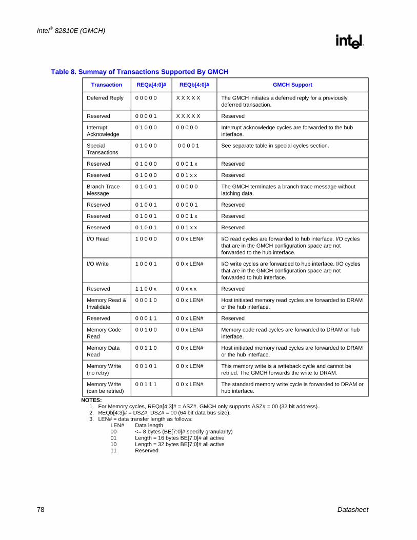
Intel® 82810E (GMCH)
R
78 Datasheet
Table 8. Summay of Transactions Supported By GMCH
Transaction REQa[4:0]# REQb[4:0]# GMCH Support
Deferred Reply 0 0 0 0 0 X X X X X The GMCH initiates a deferred reply for a previously deferred transaction.
Reserved 0 0 0 0 1 X X X X X Reserved
Interrupt Acknowledge
0 1 0 0 0 0 0 0 0 0 Interrupt acknowledge cycles are forwarded to the hub interface.
Special Transactions
0 1 0 0 0 0 0 0 0 1 See separate table in special cycles section.
Reserved 0 1 0 0 0 0 0 0 1 x Reserved
Reserved 0 1 0 0 0 0 0 1 x x Reserved
Branch Trace Message
0 1 0 0 1 0 0 0 0 0 The GMCH terminates a branch trace message without latching data.
Reserved 0 1 0 0 1 0 0 0 0 1 Reserved
Reserved 0 1 0 0 1 0 0 0 1 x Reserved
Reserved 0 1 0 0 1 0 0 1 x x Reserved
I/O Read 1 0 0 0 0 0 0 x LEN# I/O read cycles are forwarded to hub interface. I/O cycles that are in the GMCH configuration space are not forwarded to the hub interface.
I/O Write 1 0 0 0 1 0 0 x LEN# I/O write cycles are forwarded to hub interface. I/O cycles that are in the GMCH configuration space are not forwarded to hub interface.
Reserved 1 1 0 0 x 0 0 x x x Reserved
Memory Read & Invalidate
0 0 0 1 0 0 0 x LEN# Host initiated memory read cycles are forwarded to DRAM or the hub interface.
Reserved 0 0 0 1 1 0 0 x LEN# Reserved
Memory Code Read
0 0 1 0 0 0 0 x LEN# Memory code read cycles are forwarded to DRAM or hub interface.
Memory Data Read
0 0 1 1 0 0 0 x LEN# Host initiated memory read cycles are forwarded to DRAM or the hub interface.
Memory Write (no retry)
0 0 1 0 1 0 0 x LEN# This memory write is a writeback cycle and cannot be retried. The GMCH forwards the write to DRAM.
Memory Write (can be retried)
0 0 1 1 1 0 0 x LEN# The standard memory write cycle is forwarded to DRAM or hub interface.
NOTES: 1. For Memory cycles, REQa[4:3]# = ASZ#. GMCH only supports ASZ# = 00 (32 bit address). 2. REQb[4:3]# = DSZ#. DSZ# = 00 (64 bit data bus size). 3. LEN# = data transfer length as follows:
LEN# Data length 00 <= 8 bytes (BE[7:0]# specify granularity) 01 Length = 16 bytes BE[7:0]# all active 10 Length = 32 bytes BE[7:0]# all active 11 Reserved

Intel® 82810E (GMCH)
R
Datasheet 79
Table 9. Host Responses Supported by the GMCH
RS2# RS1# RS0# Description GMCH Support
0 0 0 idle
0 0 1 Retry Response This response is generated if an access is to a resource that cannot be accessed by the processor at this time and the logic must avoid deadlock . Hub interface directed reads, writes, and DRAM locked reads can be retried.
0 1 0 Deferred Response
This response can be returned for all transactions that can be executed ‘out of order.’ Hub interface directed reads (memory, I/O and Interrupt Acknowledge) and writes (I/O only), and internal Graphics device directed reads (memory and I/O) and writes (I/O only) can be deferred.
0 1 1 Reserved Reserved
1 0 0 Hard Failure Not supported.
1 0 1 No Data Response
This is for transactions where the data has already been transferred or for transactions where no data is transferred. Writes and zero length reads receive this response.
1 1 0 Implicit Writeback
This response is given for those transactions where the initial transactions snoop hits on a modified cache line.
1 1 1 Normal Data Response
This response is for transactions where data accompanies the response phase. Reads receive this response.

Intel® 82810E (GMCH)
R
80 Datasheet
4.2.2. Special Cycles
A Special Cycle is defined when REQa[4:0] = 01000 and REQb[4:0]= xx001. The first address phase Aa[35:3]# is undefined and can be driven to any value. The second address phase, Ab[15:8]# defines the type of Special Cycle issued by the processor.
Table 10 specifies the cycle type and definition as well as the action taken by the GMCH when the corresponding cycles are identified.
Table 10. Special Cycles
BE[7:0}# Special Cycle Type Action Taken
0000 0000 NOP This transaction has no side-effects.
0000 0001 Shutdown This transaction is issued when an agent detects a severe software error that prevents further processing. This cycle is claimed by the GMCH. The GMCH issues a shutdown special cycle on the hub interface. This cycle is retired on the processor bus after it is terminated on the hub interface via a master abort mechanism.
0000 0010 Flush This transaction is issued when an agent has invalidated its internal caches without writing back any modified lines. The GMCH claims this cycle and retires it.
0000 0011 Halt This transaction is issued when an agent executes a HLT instruction and stops program execution. This cycle is claimed by the GMCH and propagated to the hub interface as a Special Halt Cycle. This cycle is retired on the processor bus after it is terminated on the hub interface via a master abort mechanism.
0000 0100 Sync This transaction is issued when an agent has written back all modified lines and has invalidated its internal caches. The GMCH claims this cycle and retires it.
0000 0101 Flush Acknowledge This transaction is issued when an agent has completed a cache sync and flush operation in response to an earlier FLUSH# signal assertion. The GMCH claims this cycle and retires it.
0000 0110 Stop Clock Acknowledge This transaction is issued when an agent enters Stop Clock mode. This cycle is claimed by the GMCH and propagated to the hub interface as a Special Stop Grant Cycle. This cycle is completed on the processor bus after it is terminated on the hub interface via a master abort mechanism.
0000 0111 SMI Acknowledge This transaction is first issued when an agent enters the System Management Mode (SMM). Ab[7]# is also set at this entry point. All subsequent transactions from the processor with Ab[7]# set are treated by the GMCH as accesses to the SMM space. No corresponding cycle is propagated to the hub interface. To exit the System Management Mode the processor issues another one of these cycles with the Ab[7]# bit deasserted. The SMM space access is closed by the GMCH at this point.
all others Reserved
Intel® 82810E (GMCH)
R
Datasheet 81
4.3. System Memory DRAM Interface The GMCH integrates a system DRAM controller that supports a 64-bit DRAM array. The DRAM type supported is Synchronous (SDRAM). The GMCH generates the SCS#, SDQM, SCAS#, SRAS#, SWE# and multiplexed addresses, SMA for the DRAM array. The GMCH’s DRAM interface operates at a clock frequency of 100 MHz, independent of the system bus interface clock frequency. The DRAM controller interface is fully configurable through a set of control registers. Complete descriptions of these registers are given in the Chapter 3, “Configuration Registers”.
The GMCH supports industry standard 64-bit wide DIMM modules with SDRAM devices. The 2 bank select lines SBS[1:0], the 12 Address lines SMAA[11:0], and second copies of 4 Address lines SMAB[7:4]# allow the GMCH to support 64-bit wide DIMMs using 16Mb, 64Mb, or 128Mb technology SDRAMs. The GMCH has four SCS# lines, enabling the support of up to four 64-bit rows of DRAM. For write operations of less than a QWord in size, the GMCH will perform a byte-wise write. The GMCH targets SDRAM with CL2 and CL3 and supports both single and double-sided DIMMs. The GMCH provides refresh functionality with programmable rate (normal DRAM rate is 1 refresh/15.6 µs). The GMCH can be configured via the Page Closing Policy Bit in the GMCH Configuration Register to keep multiple pages open within the memory array. Pages can be kept open in any one row of memory. Up to 4 pages can be kept open within that row (The GMCH only supports 4 Bank SDRAMs on system DRAM interface).
4.3.1. DRAM Organization and Configuration
The GMCH supports 64-bit DRAM configurations. In the following discussion the term row refers to a set of memory devices that are simultaneously selected by a SCS# signal. The GMCH will support a maximum of 4 rows of memory. Both single-sided and double-sided DIMMs are supported.
The interface consists of the following pins:
Multiple copies: SMAA[7:4], SMAB[7:4]#
Single Copies: SMD[63:0] SDQM[7:0] SMAA[11:8,3:0] SBS[1:0] SCS[3:0]# SCAS# SRAS# SWE# SCKE[1:0]
The GMCH supports DIMMs populated with 8, 16, and 32 bit wide SDRAM devices. Registered DIMMs or DIMMs populated with 4 bit wide SDRAM devices are not supported. The GMCH supports 3.3V standard SDRAMs.
Table 11 illustrates a sample of the possible DIMM socket configurations along with corresponding DRP programming. See the register section of this document for a complete DRP programming table.

Intel® 82810E (GMCH)
R
82 Datasheet
Table 11. Sample Of Possible Mix And Match Options For 4 Row/2 DIMM Configurations
DIMM0 DIMM1 DRP Total Memory
0 4x(4M x 16 ) S 70 32 MB
4x (4M x16 ) S 0 07 32 MB
4x(4Mx16) + 2x(2Mx32) D 0 08 48 MB
4x(4Mx16) S 4x(4Mx16) S 77 64 MB
8x(8Mx8) + 4x(4Mx16) D 0 0B 96 MB
8x(8Mx8) D 0 0C 128 MB
8x(8Mx8) D 8x(8Mx8) D CC 256 MB NOTES:
1. "S" denotes single-sided DIMM's, "D" denotes double-sided DIMM's.
4.3.1.1. Configuration Mechanism For DIMMs
Detection of the type of DRAM installed on the DIMM is supported via Serial Presence Detect mechanism as defined in the JEDEC 168-pin DIMM standard. This standard uses the SCL, SDA and SA[2:0] pins on the DIMMs to detect the type and size of the installed DIMMs. No special programmable modes are provided on the GMCH for detecting the size and type of memory installed. Type and size detection must be done via the serial presence detection pins. Use of Serial Presence Detection is required.
Memory Detection and Initialization
Before any cycles to the memory interface can be supported, the GMCH DRAM registers must be initialized. The GMCH must be configured for operation with the installed memory types. Detection of memory type and size is done via the System Management Bus (SMBus) interface on the ICH. This 2-wire bus is used to extract the DRAM type and size information from the serial presence detect port on the DRAM DIMM modules.
DRAM DIMM modules contain a 5 pin serial presence detect interface, including SCL (serial clock), SDA (serial data) and SA[2:0]. Devices on the SMBus bus have a seven bit address. For the DRAM DIMM modules, the upper four bits are fixed at 1010. The lower three bits are strapped on the SA[2:0] pins. SCL and SDA are connected directly to the System Management Bus on the ICH. Thus data is read from the Serial Presence Detect port on the DRAM DIMM modules via a series of IO cycles to the ICH. BIOS essentially needs to determine the size and type of memory used for each of the four rows of memory in order to properly configure the GMCH system memory interface.
SMBus Configuration and Access of the Serial Presence Detect Ports
For more details on this see the Intel® 82801AA (ICH) and Intel® 82801AB (ICH0) I/O Controller Hub datasheet.
4.3.1.2. DRAM Register Programming
This section provides an overview of how the required information for programming the DRAM registers is obtained from the Serial Presence Detect ports on the DIMMs. The Serial Presence Detect ports are used to determine Refresh Rate, MA and MD Buffer Strength, Row Type (on a row by row basis), SDRAM Timings, Row Sizes and Row Page Sizes. Table 12 lists a subset of the data available through the on-board Serial Presence Detect ROM on each DIMM module.

Intel® 82810E (GMCH)
R
Datasheet 83
Table 12. Data Bytes on DIMM Used for Programming DRAM Registers
Byte Function
2 Memory Type (EDO, SDRAM) the GMCH only supports SDRAM.
3 # of Row Addresses, not counting Bank Addresses
4 # of Column Addresses
5 # of banks of DRAM (Single or Double sided) DIMM
12 Refresh Rate
17 # Banks on each SDRAM Device
36-41 Access Time from Clock for CAS# Latency 1 through 7
42 Data Width of SDRAM Components
Table 12 is only a subset of the defined SPD bytes on the DIMM module. These bytes collectively provide enough data for BIOS to program the GMCH DRAM registers.
4.3.2. DRAM Address Translation and Decoding
The GMCH contains address decoders that translate the address received on the host bus, hub interface, or from the internal Graphics device to an effective memory address. The GMCH supports 16 and 64 Mbit SDRAM devices. The GMCH supports a 2 KB page sizes only. The multiplexed row / column address to the DRAM memory array is provided by the SBS[1:0] and SMAA[11:0] signals and copies. These addresses are derived from the host address bus as defined by by the following table for SDRAM devices.
Row size is internally computed using the values programmed in the DRP register.
Up to 4 pages can be open at any time within any row (Only 2 active pages are supported in rows populated with either 8 MBs or 16 MBs ).

Intel® 82810E (GMCH)
R
84 Datasheet
Table 13. GMCH DRAM Address Mux Function
Address Usage BS SMAA Tech Depth Wid
Row Col Bk
Mem Size
1 0 11 10 9 8 7 6 5 4 3 2 1 0
16Mb 1MB 16 11 8 1 8MB X 11 X [A] 22 21 20 19 18 17 16 15 14 13
X 11 X PA X X 10 9 8 7 6 5 4 3
16Mb 2MB 8 11 9 1 16MB X 11 X [A] 22 21 20 19 18 17 16 15 14 13
X 11 X PA X 23 10 9 8 7 6 5 4 3
64Mb 2MB 32 11 8 2 16MB 12 11 X [A] 22 21 20 19 18 17 16 15 14 13
12 11 X PA X X 10 9 8 7 6 5 4 3
64Mb 4MB 16 12 8 2 32MB 12 11 24 [A] 22 21 20 19 18 17 16 15 14 13
12 11 X PA X X 10 9 8 7 6 5 4 3
64Mb 8MB 8 12 9 2 64MB 12 11 24 [A] 22 21 20 19 18 17 16 15 14 13
12 11 X PA X 25 10 9 8 7 6 5 4 3
128Mb 4MB 32 12 8 2 32MB 12 11 24 [A] 22 21 20 19 18 17 16 15 14 13
12 11 X PA X X 10 9 8 7 6 5 4 3
128Mb 8MB 16 12 9 2 64MB 12 11 24 [A] 22 21 20 19 18 17 16 15 14 13
12 11 X PA X 25 10 9 8 7 6 5 4 3
128Mb 16MB 8 12 10 2 128MB 12 11 24 [A] 22 21 20 19 18 17 16 15 14 13
12 11 X PA 26 25 10 9 8 7 6 5 4 3
NOTES: 1. [A]; MA bit 10 at RAS time uses the XOR of Address bit 12 and Address bit 23
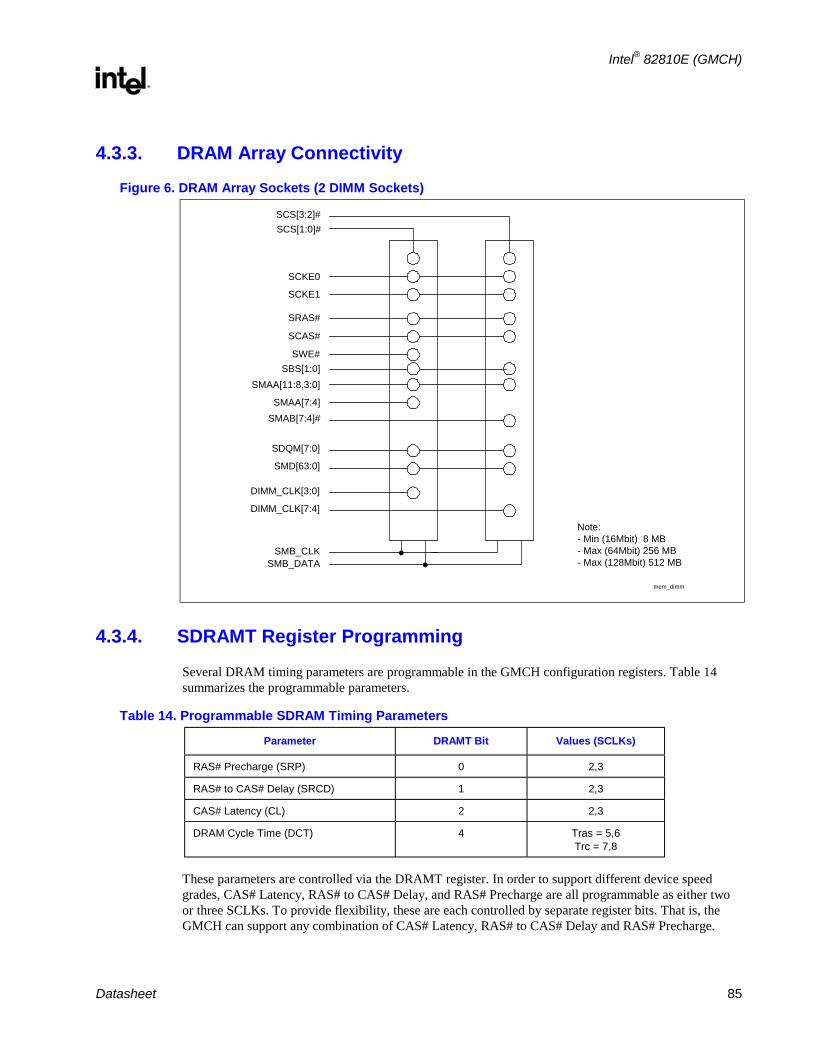
Intel® 82810E (GMCH)
R
Datasheet 85
4.3.3. DRAM Array Connectivity Figure 6. DRAM Array Sockets (2 DIMM Sockets)
SCS[3:2]#SCS[1:0]#
SCKE0
SCKE1
SRAS#
SCAS#
SWE#SBS[1:0]
SMAA[11:8,3:0]
SMAA[7:4]SMAB[7:4]#
SDQM[7:0]
SMD[63:0]
DIMM_CLK[3:0]
DIMM_CLK[7:4]
SMB_CLKSMB_DATA
Note:- Min (16Mbit) 8 MB- Max (64Mbit) 256 MB- Max (128Mbit) 512 MB
mem_dimm
4.3.4. SDRAMT Register Programming
Several DRAM timing parameters are programmable in the GMCH configuration registers. Table 14 summarizes the programmable parameters.
Table 14. Programmable SDRAM Timing Parameters
Parameter DRAMT Bit Values (SCLKs)
RAS# Precharge (SRP) 0 2,3
RAS# to CAS# Delay (SRCD) 1 2,3
CAS# Latency (CL) 2 2,3
DRAM Cycle Time (DCT) 4 Tras = 5,6 Trc = 7,8
These parameters are controlled via the DRAMT register. In order to support different device speed grades, CAS# Latency, RAS# to CAS# Delay, and RAS# Precharge are all programmable as either two or three SCLKs. To provide flexibility, these are each controlled by separate register bits. That is, the GMCH can support any combination of CAS# Latency, RAS# to CAS# Delay and RAS# Precharge.

Intel® 82810E (GMCH)
R
86 Datasheet
4.3.5. SDRAM Paging Policy
The GMCH can maintain up to 4 active pages in any one row; however, the GMCH does not support active pages in more than 1 row at a time.
The DRAM page closing policy (DPCP) in the GMCH configuration register (GMCHCFG) controls the page closing policy of the GMCH. This bit controls whether the GMCH precharges bank or precharge all during the service of a page miss. When this bit is 0, the GMCH prechanges bank during the service of a page miss. When this bit is 1, the GMCH prechanges all during the service of a page miss.
4.4. Intel Dynamic Video Memory Technology (D.V.M.T.) The internal graphics device on the 810E supports Intel Dynamic Video Memory Technology (D.V.M.T.). D.V.M.T. dynamically responds to application requirements by allocating the proper amount of display and texturing memory. For more details, refer to the document entitled, “Intel 810 Chipset: Great Performance for Value PCs” available at:
http://developer.intel.com/design/chipsets/810/810white.htm.
In addition to D.V.M.T., the 82810E supports Display Cache (DC). The graphics engine of the 82810E uses DC for implementing rendering buffers (e.g., Z buffers). This rendering model requires 4 MB of display cache and allows graphics rendering (performed across the graphics display cache bus) and texture MIP map access (performed across the system memory bus) simultaneously. Using D.V.M.T. all graphics rendering is implemented in system memory. The system memory bus is arbitrated between texture MIP-map accesses and rendering functions.
4.5. Display Cache Interface The GMCH Display Cache (DC) is a single channel 32 bit wide SDRAM interface. The DC handles the control and timing for the display cache. The display cache interface of the GMCH generates the LCS#, LDQM[7:0], LSCAS#, LSRAS#, LWE#, LMD[31:0] and multiplexed addresses, LMA[11:0] for the display cache DRAM array. The GMCH also generates the clock LTCLK for write cycles as well as LOCLK for read cycle timings.
The display cache interface of the GMCH supports single data rate synchronous dynamic random access memory (SDRAM). It supports a single 32-bit wide memory channel. The interface handles the operation of D.V.M. with DC at 100/133 MHz. The DRAM controller interface is fully configurable through a set of control registers.
Internal buffering (FIFOs) of the data to and from the display cache ensures the synchronization of the data to the internal pipelines. The D.V.M. with DC interface clocking is divided synchronous with respect to the core and system bus

Intel® 82810E (GMCH)
R
Datasheet 87
4.5.1. Supported DRAM Types
Only 1Mx16 SDRAMs are supported by the GMCH.
4.5.2. Memory Configurations
Table 15 gives a summary of the characteristics of memory configurations supported. The GMCH supports a 32-bit wide channel populated with a single row of 1Mx16 SDRAMs.
Table 15. Memory Size for Each Configuration
SDRAM SDRAM SDRAM # of Address Size DRAM DRAM Size
Tech. Density Width Banks Bank Row Column Addressing
16 Mbit 1M 16 2 1 11 8 Asymmetric 4MB
Figure 7 shows the GMCH LMI connected to 4 MB of memory in a 32-bit SDRAM channel configuration.
Figure 7. GMCH Display Cache Interface to 4 MB
GMCH
(2) 1M x 16SDRAM
LOC
LK
LRC
LK
LTCLK
LDQ
M[3:0]
LMD
[31:0]
LMA[11:0]
LWE#
LSCAS
LSRAS
LCS#
Dply_C_inter
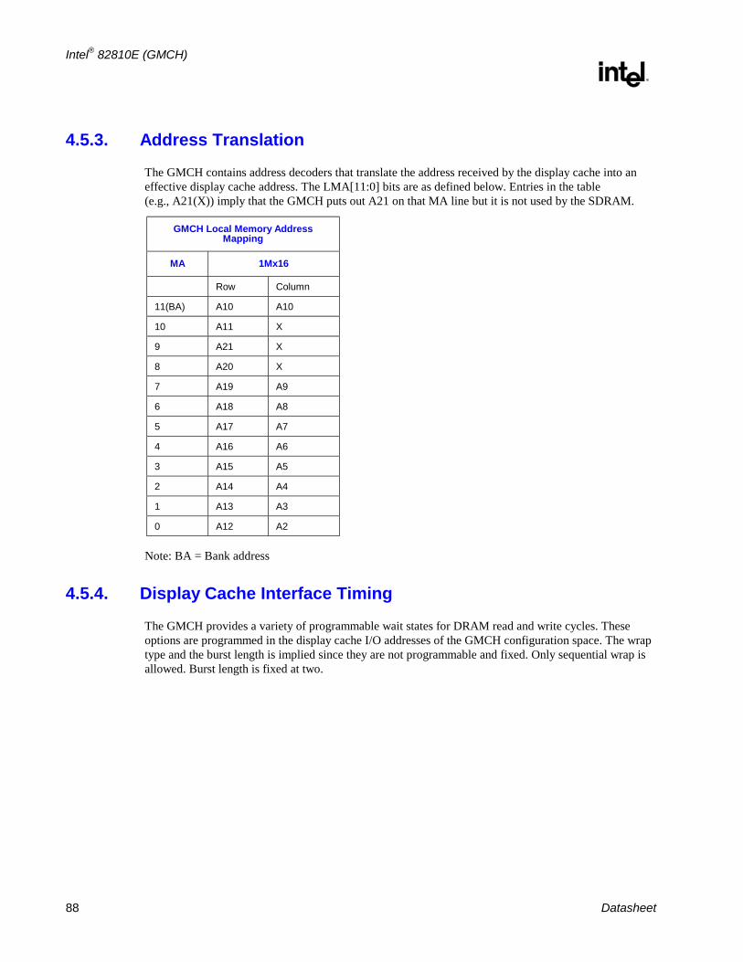
Intel® 82810E (GMCH)
R
88 Datasheet
4.5.3. Address Translation
The GMCH contains address decoders that translate the address received by the display cache into an effective display cache address. The LMA[11:0] bits are as defined below. Entries in the table (e.g., A21(X)) imply that the GMCH puts out A21 on that MA line but it is not used by the SDRAM.
GMCH Local Memory Address Mapping
MA 1Mx16
Row Column
11(BA) A10 A10
10 A11 X
9 A21 X
8 A20 X
7 A19 A9
6 A18 A8
5 A17 A7
4 A16 A6
3 A15 A5
2 A14 A4
1 A13 A3
0 A12 A2
Note: BA = Bank address
4.5.4. Display Cache Interface Timing
The GMCH provides a variety of programmable wait states for DRAM read and write cycles. These options are programmed in the display cache I/O addresses of the GMCH configuration space. The wrap type and the burst length is implied since they are not programmable and fixed. Only sequential wrap is allowed. Burst length is fixed at two.
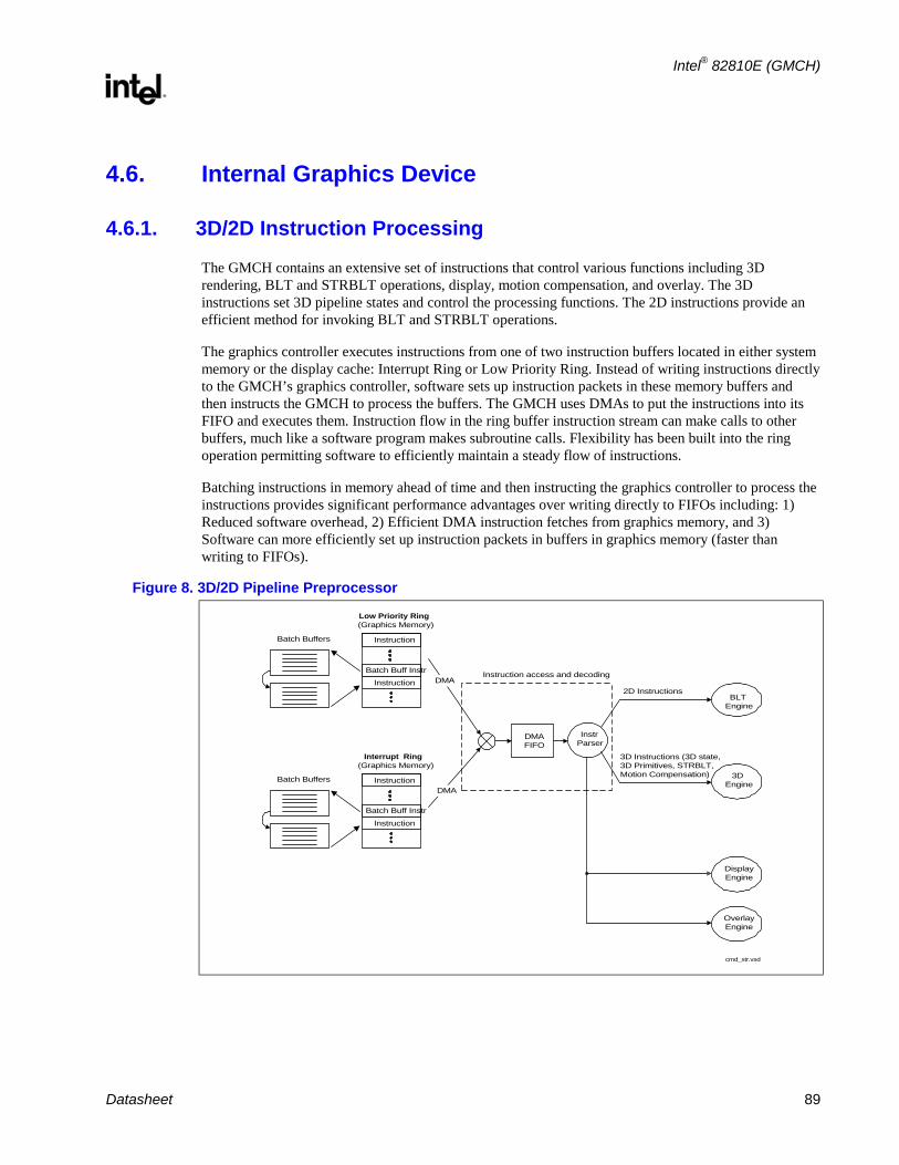
Intel® 82810E (GMCH)
R
Datasheet 89
4.6. Internal Graphics Device
4.6.1. 3D/2D Instruction Processing
The GMCH contains an extensive set of instructions that control various functions including 3D rendering, BLT and STRBLT operations, display, motion compensation, and overlay. The 3D instructions set 3D pipeline states and control the processing functions. The 2D instructions provide an efficient method for invoking BLT and STRBLT operations.
The graphics controller executes instructions from one of two instruction buffers located in either system memory or the display cache: Interrupt Ring or Low Priority Ring. Instead of writing instructions directly to the GMCH’s graphics controller, software sets up instruction packets in these memory buffers and then instructs the GMCH to process the buffers. The GMCH uses DMAs to put the instructions into its FIFO and executes them. Instruction flow in the ring buffer instruction stream can make calls to other buffers, much like a software program makes subroutine calls. Flexibility has been built into the ring operation permitting software to efficiently maintain a steady flow of instructions.
Batching instructions in memory ahead of time and then instructing the graphics controller to process the instructions provides significant performance advantages over writing directly to FIFOs including: 1) Reduced software overhead, 2) Efficient DMA instruction fetches from graphics memory, and 3) Software can more efficiently set up instruction packets in buffers in graphics memory (faster than writing to FIFOs).
Figure 8. 3D/2D Pipeline Preprocessor
DMAFIFO
InstrParser
3D Instructions (3D state,3D Primitives, STRBLT,Motion Compensation)
2D Instructions
cmd_str.vsd
3DEngine
BLTEngine
Instruction access and decoding
Low Priority Ring(Graphics Memory)
Instruction
Batch Buff Instr
Batch Buffers
Instruction
DisplayEngine
OverlayEngine
Interrupt Ring(Graphics Memory)
Instruction
Batch Buff Instr
Instruction
Batch BuffersDMA
DMA

Intel® 82810E (GMCH)
R
90 Datasheet
4.6.2. 3D Engine
The 3D engine of the GMCH has been architected as a deep pipeline, where performance is maximized by allowing each stage of the pipeline to simultaneously operate on different primitives or portions of the same primitive. The internal graphics device of the GMCH supports perspective-correct texture mapping, bilinear and anisotropic MIP mapping, gouraud shading, alpha-blending, fogging and Z Buffering. These features can be independently enabled or disabled via set of 3D instructions. This frees up the display cache for other uses (e.g., back and depth buffers, bitmaps, etc.). In addition, the GMCH supports a Dynamic Video Memory (D.V.M.) that allows the entire 3D rendering process to take place in system memory; thus, alleviating the need for the display cache.
The main blocks of the pipeline are the Setup Engine, Scan Converter, Texture Pipeline, and Color Calculator block. A typical programming sequence would be to send instructions to set the state of the pipeline followed by rendering instructions containing 3D primitive vertex data.
4.6.3. Buffers
The 2D, 3D and video capabilities of the internal graphics device of the GMCH provide control over a variety of graphics buffers that can be implemented either in display cache or system memory. To aid the rendering process, the display cache of the GMCH contains two hardware buffers—the Front Buffer (display buffer) and the Back Buffer (rendering buffer). The image being drawn is not visible until the scene is complete and the back buffer made visible (via an instruction) or copied to the front buffer (via a 2D BLT operation). By rendering to one and displaying from the other, the possibility of image tearing is removed. This also speeds up the display process over a single buffer.
The 3D pipeline of the GMCH operates on the Back Buffer and the Z Buffer. The pixels’ 16-bit (or 15-bit) RGB colors are stored in the back buffer. The Z-buffer can be used to store 16-bit depth values or 5-bit “destination alpha” values. The Instruction set of the GMCH provides a variety of controls for the buffers (e.g., initializing, flip, clear, etc.).

Intel® 82810E (GMCH)
R
Datasheet 91
Figure 9. Data Flow for the 3D Pipeline
Notes:1. Frame Buffer = Front and Back Buffers
3d_pipe2
Depth Buffer(Z-Buffer)
Display Cache
System Memory
Textures
Instructionsand Data
GMCHInterface
PrimitivesPixels
MappingEngine Color
Calculator Rasterize
Setup Discard(Back Face
Culling)Frame Buffer
GMCH Graphics Pipeline(Conceptual Representation)
4.6.4. Setup
The setup stage of the pipeline takes the input data associated with each vertex of the line or triangle primitive and computes the various parameters required for scan conversion. In formatting this data, the GMCH maintains sub-pixel accuracy. Data is dynamically formatted for each rendered polygon and output to the proper processing unit. As part of the setup, the GMCH removes polygons from further processing, if they are not facing the user’s viewpoint (referred to as “ Back Face Culling”).

Intel® 82810E (GMCH)
R
92 Datasheet
4.6.5. Texturing
The internal graphics device of the GMCH allows an image, pattern, or video to be placed on the surface of a 3D polygon. Textures must be located in system memory. Being able to use textures directly from system memory means that large complex textures can easily be handled without the limitations imposed by the traditional approach of only using the display cache.
The texture processor receives the texture coordinate information from the setup engine and the texture blend information from the scan converter. The texture processor performs texture color or chroma-key matching, texture filtering (anisotropic and bilinear interpolation), and YUV to RGB conversions.
The GMCH supports up to 11 Levels-of-Detail (LODs) ranging in size from 1024x1024 to 1x1 texels. (A texel is defined as a texture map pixel). Textures need not be square. Included in the texture processor is a small cache that provides efficient mip-mapping.
• Nearest. Texel with coordinates nearest to the desired pixel is used. (This is used if only one LOD is present).
• Linear. A weighted average of a 2x2 area of texels surrounding the desired pixel are used. (This is used if only one LOD is present).
• Mip Nearest. This is used if many LODs are present. The appropriate LOD is chosen and the texel with coordinates nearest to the desired pixel are used.
• Mip Linear. This is used if many LODs are present. The appropriate LOD is chosen and a weighted average of a 2x2 area of texels surrounding the desired pixel are used. This is also referred to as bi-linear mip-mapping.
• Anisotropic. This can be used if multiple LODs are present. This filtering method improves the visual quality of texture-mapped objects when viewed at oblique angles (i.e., with a high degree of perspective foreshortening). The improvement comes from a more accurate (anisotropic) mapping of screen pixels onto texels -- where using bilinear or trilinear filtering can yield overly-blurred results. Situations where anisotropic filtering demonstrates superior quality include text viewed at an angle, lines on roadways, etc.
Intel® 82810E (GMCH)
R
Datasheet 93
The GMCH can store each of the above mip-maps in any of the following formats:
• 8bpt Surface Format
• 16bpt Surface Format RGB 565 ARGB 1555 ARGB 4444 AY 88
• 8bpt (Indexed) Surface Format RGB 565 ARGB 1555 ARGB 4444 AY 88
• 4:2:2 YCrCb, Swap Y Format YCrCb, Normal YCrCb, UV Swap YCrCb, UV/Y Swap
Many texture mapping modes are supported. Perspective correct mapping is always performed. As the map is fitted across the polygon, the map can be tiled, mirrored in either the U or V directions, or mapped up to the end of the texture and no longer placed on the object (this is known as clamp mode). The way a texture is combined with other object attributes is also definable.
Texture ColorKey and ChromaKey
ColorKey and ChromaKey describe two methods of removing a specific color or range of colors from a texture map before it is applied to an object. For “nearest” texture filter modes, removing a color simply makes those portions of the object transparent (the previous contents of the back buffer show through). For “ linear “ texture filtering modes, the texture filter is modified if only the non-nearest neighbor texels match the key (range).
ColorKeying occurs with paletted textures, and removes colors according to an index (before the palette is accessed). When a color palette is used with indices to indicate a color in the palette, the indices can be compared against a state variable “ColorKey Index Value” and if a match occurs and ColorKey is enabled, then this value’s contribution is removed from the resulting pixel color. The GMCH defines index matching as ColorKey.
ChromaKeying can be performed for both paletted and non-paletted textures, and removes texels that fall within a specified color range. The ChromaKey mode refers to testing the RGB or YUV components to see if they fall between high and low state variable values. If the color of a texel contribution is in this range and chromaKey is enabled, then this contribution is removed from the resulting pixel color.
Multiple Texture Composition
The GMCH includes support for two simultaneous texture maps. This support greatly reduces the need for multipass compositing techniques for effects such as diffuse light maps, specular reflection maps, bump mapping, detail textures, gloss maps, shadows, and composited effects like dirt or tire marks. Supporting these techniques in hardware greatly increases compositing performance by reducing the need to read and write the frame buffer multiple times.
Intel® 82810E (GMCH)
R
94 Datasheet
This multitexture support provides a superset of the “legacy” one-texture (pre-DirectX 6) texture blend modes and a large subset of the operations defined in DirectX 6 and the OpenGL ARB multitexture extensions.
The Multitexture Compositing Unit is capable of combining the interpolated vertex diffuse color, a constant color value, and up to two texels per pixel in a fully-programmable fashion. Up to three operations (combinations) can be performed in a pipelined organization, with intermediate storage to support complex equations, e.g., of the form “A*B + C*D” required for light maps and specular gloss maps. Separate operations can be performed on color (RGB) and alpha components.
4.6.6. 2D Operation
The GMCH contains BLT and STRBLT functionality, a hardware cursor, and an extensive set of 2D registers and instructions.
GMCH VGA Registers and Enhancements
The 2D registers are a combination of registers defined by IBM* when the Video Graphics Array (VGA) was first introduced, and others that Intel has added to support graphics modes that have color depths, resolutions, and hardware acceleration features that go beyond the original VGA standard. The internal graphics device of the GMCH improves upon VGA by providing additional features that are used through numerous additional registers.
The GMCH also supports an optional display cache. As an improvement on the VGA standard display cache port-hole, the GMCH also maps the entire display cache into part of a single contiguous memory space at a programmable location, providing what is called “linear” access to the display cache. The size of this memory can be up to 4 MB, and the base address is set via PCI configuration registers. Alternatively, these buffers may be implemented in system memory (via D.V.M.), thus alleviating the need for the display cache.
4.6.7. Fixed Blitter (BLT) and Stretch Blitter (STRBLT) Engines
The GMCH ‘s 64-bit BLT engine provides hardware acceleration for many common Windows* operations. The following are two primary BLT functions: Fixed Blitter (BLT) and Stretch Blitter (STRBLT). The term BLT refers to a block transfer of pixel data between memory locations. The word “fixed” is used to differentiate from the Stretch BLT engine. The BLT engine can be used for the following:
• Move rectangular blocks of data between memory locations
• Data Alignment
• Perform logical operations
The internal graphics device of the GMCH has instructions to invoke BLT and STRBLT operations, permitting software to set up instruction buffers and use batch processing as described in the 3D/2D Instruction Processing (Pipeline Preprocessor) Section. Note that these instructions replace the need to do PIO directly to BLT and STRBLT registers; this speeds up the operation.
Intel® 82810E (GMCH)
R
Datasheet 95
4.6.7.1. Fixed BLT Engine
The rectangular block of data does not change as it is transferred between memory locations. The allowable memory transfers are between: system memory and display cache, display cache and display cache, and system memory and system memory. Data to be transferred can consist of regions of memory, patterns, or solid color fills. A pattern will always be 8x8 pixels wide and may be 8, 16, or 24 bits per pixel.
The internal graphics device of the GMCH has the ability to expand monochrome data into a color depth of 8, 16, or 24 bits. BLTs can be either opaque or transparent. Opaque transfers, move the data specified to the destination. Transparent transfers, compare destination color to source color and write according to the mode of transparency selected.
Data horizontally and vertically aligned at the destination. If the destination for the BLT overlaps with the source memory location, the GMCH can specify which area in memory to begin the BLT transfer. Use of this BLT engine accelerates the Graphical User Interface (GUI) of Microsoft* Windows. Hardware is included for all 256 raster operations (Source, Pattern, and Destination) defined by Microsoft* , including transparent BLT.
4.6.7.2. Arithmetic Stretch BLT Engine
The stretch BLT function can stretch source data in the X and Y directions to a destination larger or smaller than the source. Stretch BLT functionality expands a region of memory into a larger or smaller region using replication and interpolation.
The stretch BLT engine also provides format conversion and data alignment. Through an algorithm implemented in the mapping engine, object expansion and contraction can occur in the horizontal and vertical directions.
4.6.8. Hardware Motion Compensation
The Motion Compensation (MC) process consists of reconstructing a new picture by predicting (either forward, backward or bidirectionally) the resulting pixel colors from one or more reference pictures. The GMCH intercepts the DVD pipeline at Motion Compensation and implements Motion Compensation and subsequent steps in hardware. Performing Motion Compensation in hardware reduces the processor demand of software-based MPEG-2 decoding, and thus improves system performance.
The GMCH’s implementation of Hardware Motion Compensation supports a motion smoothing algorithm. When the system processor is not able to process the MPEG decoding stream in a timely manner (as can happen in software DVD implementations), the 82810E graphics device supports downsampled MPEG decoding. Downsampling allows for reduced spatial resolution in the MPEG picture while maintaining a full frame rate, and thus reduces processor load while maintaining the best video quality possible given the processor constraints.
Intel® 82810E (GMCH)
R
96 Datasheet
4.6.9. Hardware Cursor
The internal graphics device of the GMCH allows up to an unlimited number of cursor patterns to be stored in the display cache or system memory. Two sets of registers, contain the x and y position of the cursor relative to the upper left corner of the display. The following four cursor modes are provided:
• 32x32 2 bpp AND/XOR 2-plane mode
• 64x64 2 bpp 3-color and transparency mode
• 64x64 2 bpp AND/XOR 2-plane mode
• 64x64 2 bpp 4-color mode
4.6.10. Overlay Engine
The overlay engine provides a method of merging either video capture data (from an external PCI Video Capture Adapter) or data delivered by the processor, with the graphics data on the screen. Supported data formats include YUV 4:2:2, YUV 4:2:0, YUV 4:1:0, YUV 4:1:1, RGB15, and RGB16. The source data can be mirrored horizontally or vertically or both. Overlay data comes from a buffer located system memory. Additionally, the overlay engine can be quadruple buffered in order to support flipping between different overlay images. Data can either be transferred into the overlay buffer from the host or from an external PCI adapter, such as DVD hardware or video capture hardware. Buffer swaps can be done by the host and internally synchronized with the display VBLANK.
The internal graphics device of the GMCH can accept line widths up to 720 pixels. In addition, overlay source and destination chromakeying are also supported. Overlay source/destination chromakeying enables blending of the overlay with the underlying graphics background. Destination color/chroma keying can be used to handle occluded portions of the overlay window on a pixel by pixel basis that is actually an underlay. Source color/chroma keying is used to handle transparency based on the overlay window on a pixel by pixel basis. This is used when “blue screening” an image in order to overlay the image on a new background later.
To compensate for overlay color intensity loss due to the non-linear response between display devices, the overlay engine supports independent gamma correction. In addition, the brightness, saturation, and contrast of the overlay may be independently varied.
4.6.11. Display
The display function contains a RAM-based Digital-to-Analog Converter (RAMDAC) that transforms the digital data from the graphics and video subsystems to analog data for the monitor. The GMCH’s integrated 230 MHz RAMDAC provides resolution support up to 1600x1200. Circuitry is incorporated to limit the switching noise generated by the DACs. Three 8-bit DACs provide the R, G, and B signals to the monitor. Sync signals are properly delayed to match any delays from the D-to-A conversion. Associated with each DAC is a 256 pallet of colors. The RAMDAC can be operated in either direct or indexed color mode. In Direct color mode, pixel depths of 15, 16, or 24 bits can be realized. Non-interlaced mode is supported. Gamma correction can be applied to the display output.
The GMCH supports a wide range of resolutions, color depths, and refresh rates via a programmable dot clock that has a maximum frequency of 230 MHz.
Intel® 82810E (GMCH)
R
Datasheet 97
Table 16. Partial List of Display Modes Supported
Bits Per Pixel (frequency in Hz)
Resolution 8-bit Indexed 16-bit 24-bit
320x200 70 70 70
320x240 70 70 70
352x480 70 70 70
352x576 70 70 70
400x300 70 70 70
512x384 70 70 70
640x400 70 70 70
640x480 60,70,72,75,85 60,70,72,75,85 60,70,72,75,85
720x480 75,85 75,85 75,85
720x576 60,75,85 60,75,85 60,75,85
800x600 60,70,72,75,85 60,70,72,75,85 60,70,72,75,85
1024x768 60, 70,72,75,85 60, 70,72,75,85 60, 70,72,75,85
1152x864 60,70,72,75,85 60,70,72,75,85 60,70,72,75,85
1280x720 60,75,85 60,75,85 60,75,85
1280x960 60,75,85 60,75,85 60,75,85
1280x1024 60,70,72,75,85 60,70,72,75,85 60,70,75,85
1600x900 60,75,85 60,75,85
1600x1200 60,70,72,75,85

Intel® 82810E (GMCH)
R
98 Datasheet
Table 17. Overlay Modes Supported
Pixel Resolution Colors 60Hz 70Hz 72Hz 75Hz 85Hz
256 D/Y D/Y D/Y D/Y D/Y
16 Bit D/Y D/Y D/Y D/Y D/Y
640x480
24 Bit D/Y D/Y D/Y D/Y D/Y
256 — — — D/Y D/Y
16 Bit — — — D/Y D/Y
720x480
24 Bit — — — D/Y D/Y
256 — — — D/Y D/Y
16 Bit — — — D/Y D/Y
720x576
24 Bit — — — D/Y D/Y
256 D/Y D/Y D/Y D/Y D/Y
16 Bit D/Y D/Y D/Y D/Y D/Y
800x600
24 Bit D/Y D/Y D/Y D/Y D/Y
256 D/Y D/Y — D/Y D/Y
16 Bit D/Y D/Y — D/Y D1
1024x768
24 Bit D/Y D/Y — D/Y D1
256 D/Y D/Y D/Y D/Y D1
16 Bit D/Y D/Y D1 D1 D1
1152x864
24 Bit D/Y — — D1 D1
256 D/Y D1 D1 D1 D1
16 Bit D1 D1 D1 D D
1280x1024
24 Bit D1 D1 - D D
1600x1200 256 D1 D1 D1 D — NOTES:
1. Overlay support modified in the 2.2 driver 2. D = Available Desktop Mode 3. Y = Overlay Support

Intel® 82810E (GMCH)
R
Datasheet 99
4.6.12. Flat Panel Interface / 1.8V TV-Out Interface
The GMCH has a dedicated port for Flat Panel support. This port is a 16 bit digital port (4 control bits and 12 data bits) with a 1.8V interface for high speed signaling. The port is designed to connect to transmission devices. The port can also be used to interface with an external TV encoder that requires 1.8V signals.
Connecting the GMCH to a flat panel transmitter is demonstrated below. For more details, refer to the Intel® 810E Chipset Design Guide at http://developer.intel.com/design/chipsets/designex/290675.htm.
The GMCH supports a variety of Flat Panel display modes and refresh rates that require up to a 65 MHz dot clock over this interface. Table 18 shows some of the display modes supported by the GMCH. Table 19 shows some of the TV-Out modes supported by the GMCH.
Table 18. Partial List of Flat Panel Modes Supported
Bits Per Pixel (frequency in Hz)
Resolution 8-bit Indexed 16-bit 24-bit
320x2001 60 60 60
320x2401 60 60 60
352x4801 60 60 60
352x4801 60 60 60
352x5761 60 60 60
400x3001 60 60 60
512x3841 60 60 60
640x3501 60 60 60
640x4001 60 60 60
640x4801 60 60 60
720x4801 60 60 60
720x5761 60 60 60
800x6001 60 60 60
1024x768 60 60 60 NOTES:
1. These resolutions are supported via centering.
Intel® 82810E (GMCH)
R
100 Datasheet
Table 19. Partial List of TV-Out Modes Supported
Resolution Colors NTSC PAL
320x2001 256 Yes Yes
16M Yes Yes
64k Yes Yes
320x240 256 Yes Yes
16M Yes Yes
64k Yes Yes
352x4801 256 Yes Yes
16M Yes Yes
64k Yes Yes
352x5761 256 Yes Yes
16M Yes Yes
64k Yes Yes
400x3001 256 Yes Yes
16M Yes Yes
64k Yes Yes
640x4001 256 Yes Yes
640x480 256 Yes Yes
64k Yes Yes
16M Yes Yes
720x4801 256 Yes Yes
64k Yes Yes
16M Yes Yes
720x5761 256 Yes Yes
64k Yes Yes
16M Yes Yes
800x600 16 Yes Yes
256 Yes Yes
32k Yes Yes
64k Yes Yes
16M Yes Yes NOTES:
1. These resolutions are supported via centering.
4.6.13. DDC (Display Data Channel)
DDC is a standard defined by VESA. Its purpose is to allow communication between the host system and display. Both configuration and control information can be exchanged allowing plug-and-play systems to be realized. Support for DDC 2B is implemented.
Intel® 82810E (GMCH)
R
Datasheet 101
4.7. System Reset for the GMCH Refer to the Intel 810E Chipset Design Guide (Power Sequencing section) for details.
4.8. System Clock Description The 810E Chipset is supported by a CK810E clock synthesizer. Refer to the Intel 810E Chipset Design Guide for details.
CK810E Features (56 Pin SSOP Package): • 3 copies of processor Clock 66/100/133 MHz (2.5V) [processor, GCH, ITP]
• 9 copies of 100 MHz SDRAM Clocks (3.3V) [SDRAM[0:7], DClk]
• 8 copies of PCI Clock (33 MHz ) (3.3V)
• 2 copies of APIC Clock @ 33 MHz, synchronous to processor Clock (2.5V)
• 1 copy of 48 MHz USB Clock (3.3V) [Non SSC] (Type 3 Buffer)
• 1 copy of 48 MHz DOT Clock (3.3V) [Non SSC] (See DOT Details)
• 2 copies of 3V 66 MHz Clock (3.3V)
• 1 copy of REF Clock @14.31818 MHz (3.3V)
• Ref. 14.31818 MHz Xtal Oscillator Input
• Power Down Pin
• Spread Spectrum Support
• IIC Support for turning off unused clocks
4.9. Power Management
4.9.1. Specifications Supported
The platform is compliant with the following specifications:
• APM Rev 1.2
• ACPI Rev 1.0
• PCI Power Management Rev 1.0
• PC’98/99, Rev 1.0
Intel® 82810E (GMCH)
R
102 Datasheet
4.9.2. ACPI Rev 1.0 — Support for Resume From S3 State
The 82810E enters self-refresh upon entering S3 (Suspend to RAM). The normal sequence is that the GMCH sends a “Precharge All banks” to SDRAM and then issues an “Enter Self-Refresh” command prior to actually entering the S3 state. However, the GMCH may issue an "Open Bank" command between these two commands, if the graphics portion is not correctly shut down prior to entering S3. The “Open Bank” command can adversely affect the memory interface in back-to-back repetitive S3-S0-S3-S0 testing activities.
There should be no request for access to the memory interface when entering S3. For processor initiated transfers, the ICHx guarantees this since it asserts STPCLK#. For I/O based traffic (e.g., such as PCI cards) all traffic should be stopped by the operating system, BIOS, and graphics driver combination.
Unified Memory Architecture (e.g., that used in the 810E chipset) requires additional precautions since the graphics controller shares memory directly with system memory. All graphics-initiated traffic needs to be stopped. The solution is to stop all graphics engines that request memory resources.
Software must disable all traffic generated by the GMCH graphics engines prior to entering S3. This includes display screen refresh (SR01 (I/O and memory offset address 3C5h (Index = 01h)), bit 5 = 1), Overlay (MMADR+68h), hardware cursor (Cursor Control Register, Memory Offset Address 70080h, bits 2:0 = 000), and the command streamer. The responsibility for this action can be in the operating system, in the system BIOS, or in the graphics driver.
The standard VGA mode only needs to disable the screen refresh since it does not start any other graphics traffic. Standard VGA drivers normally ensure this prior to entering S3 by setting the SR01 (I/O and memory offset address 3C5h (Index = 01h)), bit 5 = 1.
Intel® 82810E (GMCH)
R
Datasheet 103
5. Pinout and Package Information
5.1. 82810E GMCH Pinout Figure 10 and Figure 11 show the ball foot print of the 82810E. These figures represent the ballout by ball number. Table 19 provides an alphabetical signal listing of the ballout.
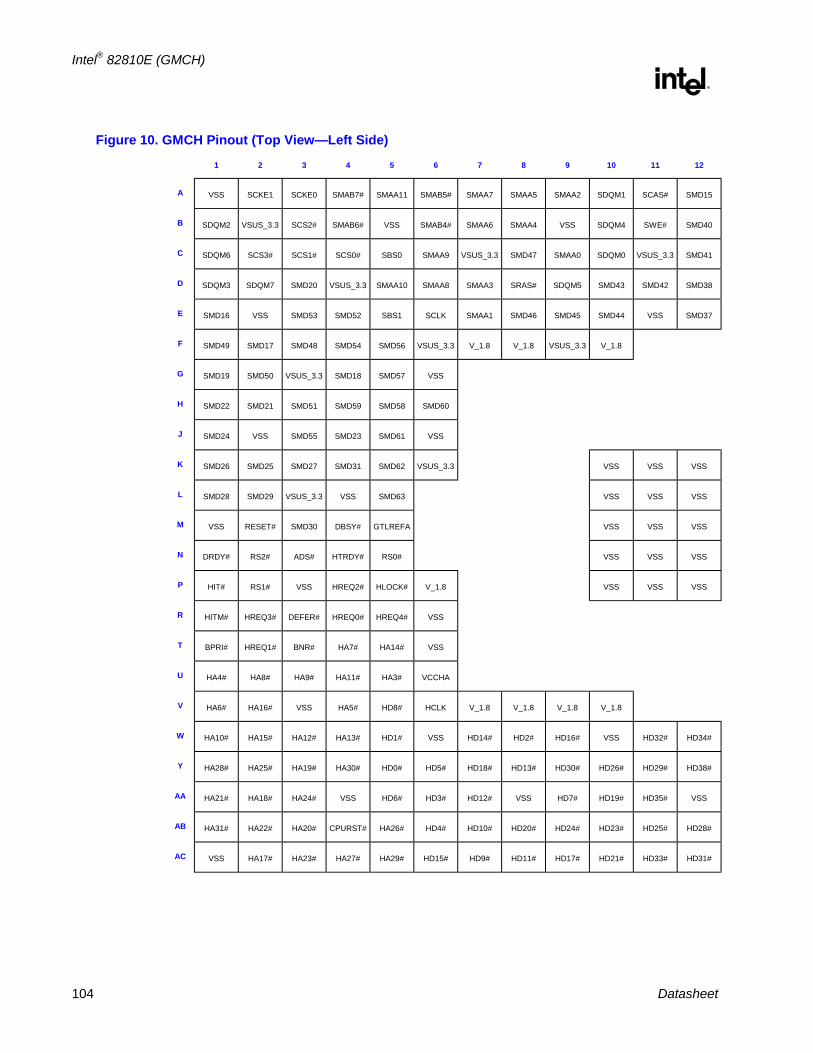
Intel® 82810E (GMCH)
R
104 Datasheet
Figure 10. GMCH Pinout (Top View—Left Side) 1 2 3 4 5 6 7 8 9 10 11 12
A VSS SCKE1 SCKE0 SMAB7# SMAA11 SMAB5# SMAA7 SMAA5 SMAA2 SDQM1 SCAS# SMD15
B SDQM2 VSUS_3.3 SCS2# SMAB6# VSS SMAB4# SMAA6 SMAA4 VSS SDQM4 SWE# SMD40
C SDQM6 SCS3# SCS1# SCS0# SBS0 SMAA9 VSUS_3.3 SMD47 SMAA0 SDQM0 VSUS_3.3 SMD41
D SDQM3 SDQM7 SMD20 VSUS_3.3 SMAA10 SMAA8 SMAA3 SRAS# SDQM5 SMD43 SMD42 SMD38
E SMD16 VSS SMD53 SMD52 SBS1 SCLK SMAA1 SMD46 SMD45 SMD44 VSS SMD37
F SMD49 SMD17 SMD48 SMD54 SMD56 VSUS_3.3 V_1.8 V_1.8 VSUS_3.3 V_1.8
G SMD19 SMD50 VSUS_3.3 SMD18 SMD57 VSS
H SMD22 SMD21 SMD51 SMD59 SMD58 SMD60
J SMD24 VSS SMD55 SMD23 SMD61 VSS
K SMD26 SMD25 SMD27 SMD31 SMD62 VSUS_3.3 VSS VSS VSS
L SMD28 SMD29 VSUS_3.3 VSS SMD63 VSS VSS VSS
M VSS RESET# SMD30 DBSY# GTLREFA VSS VSS VSS
N DRDY# RS2# ADS# HTRDY# RS0# VSS VSS VSS
P HIT# RS1# VSS HREQ2# HLOCK# V_1.8 VSS VSS VSS
R HITM# HREQ3# DEFER# HREQ0# HREQ4# VSS
T BPRI# HREQ1# BNR# HA7# HA14# VSS
U HA4# HA8# HA9# HA11# HA3# VCCHA
V HA6# HA16# VSS HA5# HD8# HCLK V_1.8 V_1.8 V_1.8 V_1.8
W HA10# HA15# HA12# HA13# HD1# VSS HD14# HD2# HD16# VSS HD32# HD34#
Y HA28# HA25# HA19# HA30# HD0# HD5# HD18# HD13# HD30# HD26# HD29# HD38#
AA HA21# HA18# HA24# VSS HD6# HD3# HD12# VSS HD7# HD19# HD35# VSS
AB HA31# HA22# HA20# CPURST# HA26# HD4# HD10# HD20# HD24# HD23# HD25# HD28#
AC VSS HA17# HA23# HA27# HA29# HD15# HD9# HD11# HD17# HD21# HD33# HD31#
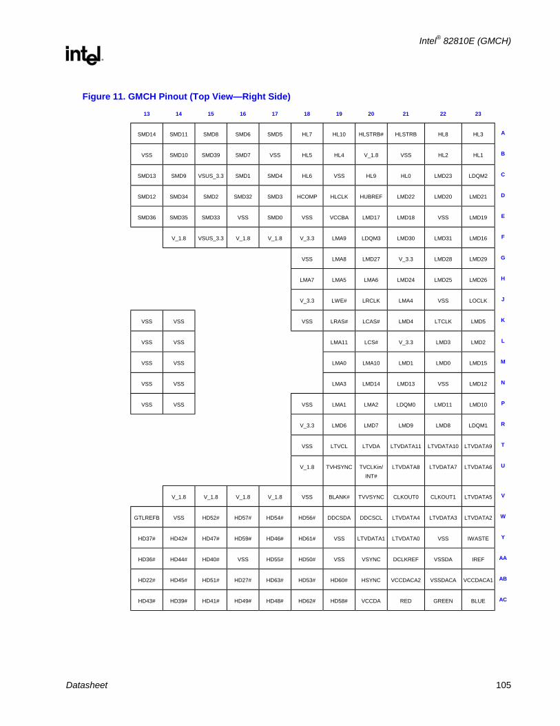
Intel® 82810E (GMCH)
R
Datasheet 105
Figure 11. GMCH Pinout (Top View—Right Side) 13 14 15 16 17 18 19 20 21 22 23
SMD14 SMD11 SMD8 SMD6 SMD5 HL7 HL10 HLSTRB# HLSTRB HL8 HL3 A
VSS SMD10 SMD39 SMD7 VSS HL5 HL4 V_1.8 VSS HL2 HL1 B
SMD13 SMD9 VSUS_3.3 SMD1 SMD4 HL6 VSS HL9 HL0 LMD23 LDQM2 C
SMD12 SMD34 SMD2 SMD32 SMD3 HCOMP HLCLK HUBREF LMD22 LMD20 LMD21 D
SMD36 SMD35 SMD33 VSS SMD0 VSS VCCBA LMD17 LMD18 VSS LMD19 E
V_1.8 VSUS_3.3 V_1.8 V_1.8 V_3.3 LMA9 LDQM3 LMD30 LMD31 LMD16 F
VSS LMA8 LMD27 V_3.3 LMD28 LMD29 G
LMA7 LMA5 LMA6 LMD24 LMD25 LMD26 H
V_3.3 LWE# LRCLK LMA4 VSS LOCLK J
VSS VSS VSS LRAS# LCAS# LMD4 LTCLK LMD5 K
VSS VSS LMA11 LCS# V_3.3 LMD3 LMD2 L
VSS VSS LMA0 LMA10 LMD1 LMD0 LMD15 M
VSS VSS LMA3 LMD14 LMD13 VSS LMD12 N
VSS VSS VSS LMA1 LMA2 LDQM0 LMD11 LMD10 P
V_3.3 LMD6 LMD7 LMD9 LMD8 LDQM1 R
VSS LTVCL LTVDA LTVDATA11 LTVDATA10 LTVDATA9 T
V_1.8 TVHSYNC TVCLKin/ INT#
LTVDATA8 LTVDATA7 LTVDATA6 U
V_1.8 V_1.8 V_1.8 V_1.8 VSS BLANK# TVVSYNC CLKOUT0 CLKOUT1 LTVDATA5 V
GTLREFB VSS HD52# HD57# HD54# HD56# DDCSDA DDCSCL LTVDATA4 LTVDATA3 LTVDATA2 W
HD37# HD42# HD47# HD59# HD46# HD61# VSS LTVDATA1 LTVDATA0 VSS IWASTE Y
HD36# HD44# HD40# VSS HD55# HD50# VSS VSYNC DCLKREF VSSDA IREF AA
HD22# HD45# HD51# HD27# HD63# HD53# HD60# HSYNC VCCDACA2 VSSDACA VCCDACA1 AB
HD43# HD39# HD41# HD49# HD48# HD62# HD58# VCCDA RED GREEN BLUE AC
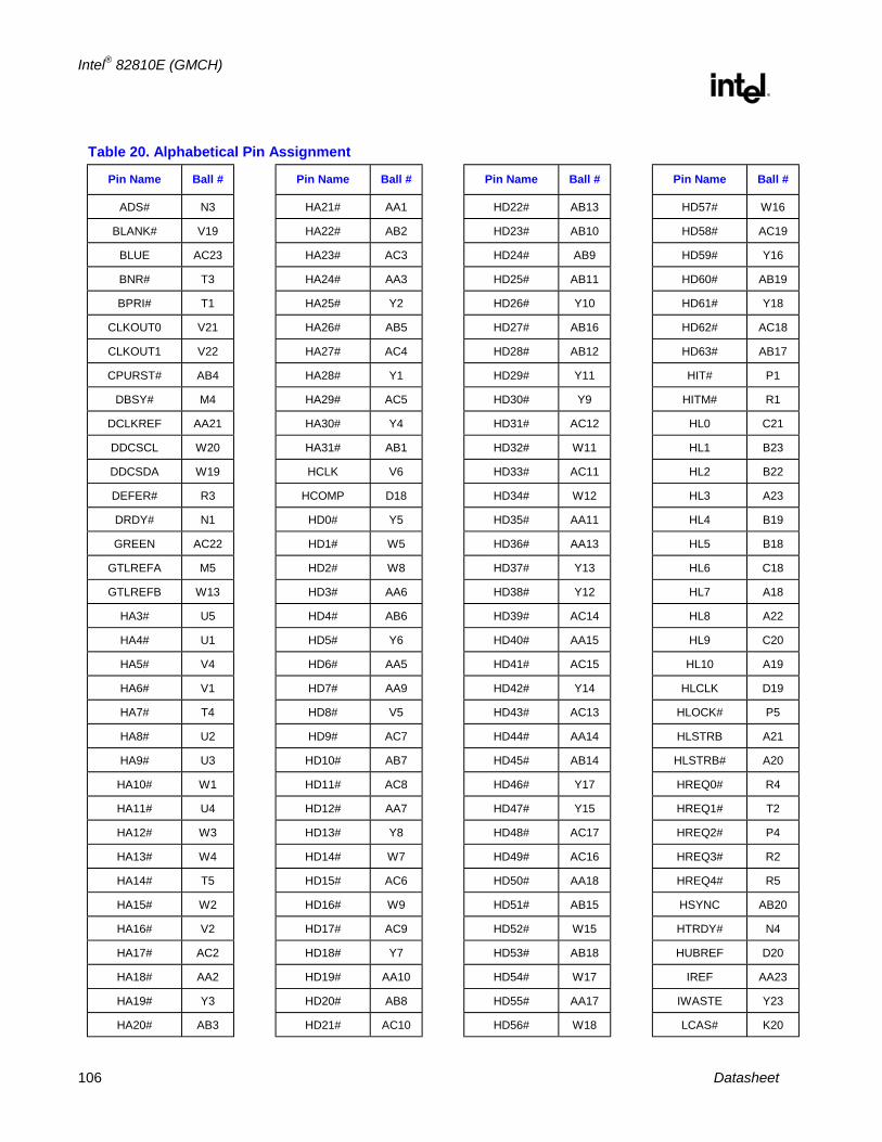
Intel® 82810E (GMCH)
R
106 Datasheet
Table 20. Alphabetical Pin Assignment
Pin Name Ball #
ADS# N3
BLANK# V19
BLUE AC23
BNR# T3
BPRI# T1
CLKOUT0 V21
CLKOUT1 V22
CPURST# AB4
DBSY# M4
DCLKREF AA21
DDCSCL W20
DDCSDA W19
DEFER# R3
DRDY# N1
GREEN AC22
GTLREFA M5
GTLREFB W13
HA3# U5
HA4# U1
HA5# V4
HA6# V1
HA7# T4
HA8# U2
HA9# U3
HA10# W1
HA11# U4
HA12# W3
HA13# W4
HA14# T5
HA15# W2
HA16# V2
HA17# AC2
HA18# AA2
HA19# Y3
HA20# AB3
Pin Name Ball #
HA21# AA1
HA22# AB2
HA23# AC3
HA24# AA3
HA25# Y2
HA26# AB5
HA27# AC4
HA28# Y1
HA29# AC5
HA30# Y4
HA31# AB1
HCLK V6
HCOMP D18
HD0# Y5
HD1# W5
HD2# W8
HD3# AA6
HD4# AB6
HD5# Y6
HD6# AA5
HD7# AA9
HD8# V5
HD9# AC7
HD10# AB7
HD11# AC8
HD12# AA7
HD13# Y8
HD14# W7
HD15# AC6
HD16# W9
HD17# AC9
HD18# Y7
HD19# AA10
HD20# AB8
HD21# AC10
Pin Name Ball #
HD22# AB13
HD23# AB10
HD24# AB9
HD25# AB11
HD26# Y10
HD27# AB16
HD28# AB12
HD29# Y11
HD30# Y9
HD31# AC12
HD32# W11
HD33# AC11
HD34# W12
HD35# AA11
HD36# AA13
HD37# Y13
HD38# Y12
HD39# AC14
HD40# AA15
HD41# AC15
HD42# Y14
HD43# AC13
HD44# AA14
HD45# AB14
HD46# Y17
HD47# Y15
HD48# AC17
HD49# AC16
HD50# AA18
HD51# AB15
HD52# W15
HD53# AB18
HD54# W17
HD55# AA17
HD56# W18
Pin Name Ball #
HD57# W16
HD58# AC19
HD59# Y16
HD60# AB19
HD61# Y18
HD62# AC18
HD63# AB17
HIT# P1
HITM# R1
HL0 C21
HL1 B23
HL2 B22
HL3 A23
HL4 B19
HL5 B18
HL6 C18
HL7 A18
HL8 A22
HL9 C20
HL10 A19
HLCLK D19
HLOCK# P5
HLSTRB A21
HLSTRB# A20
HREQ0# R4
HREQ1# T2
HREQ2# P4
HREQ3# R2
HREQ4# R5
HSYNC AB20
HTRDY# N4
HUBREF D20
IREF AA23
IWASTE Y23
LCAS# K20
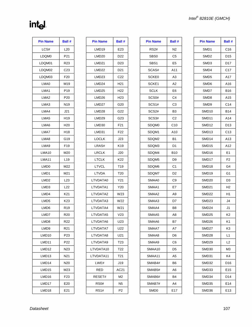
Intel® 82810E (GMCH)
R
Datasheet 107
Pin Name Ball #
LCS# L20
LDQM0 P21
LDQM01 R23
LDQM02 C23
LDQM03 F20
LMA0 M19
LMA1 P19
LMA2 P20
LMA3 N19
LMA4 J21
LMA5 H19
LMA6 H20
LMA7 H18
LMA8 G19
LMA9 F19
LMA10 M20
LMA11 L19
LMD0 M22
LMD1 M21
LMD2 L23
LMD3 L22
LMD4 K21
LMD5 K23
LMD6 R19
LMD7 R20
LMD8 R22
LMD9 R21
LMD10 P23
LMD11 P22
LMD12 N23
LMD13 N21
LMD14 N20
LMD15 M23
LMD16 F23
LMD17 E20
LMD18 E21
Pin Name Ball #
LMD19 E23
LMD20 D22
LMD21 D23
LMD22 D21
LMD23 C22
LMD24 H21
LMD25 H22
LMD26 H23
LMD27 G20
LMD28 G22
LMD29 G23
LMD30 F21
LMD31 F22
LOCLK J23
LRAS# K19
LRCLK J20
LTCLK K22
LTVCL T19
LTVDA T20
LTVDATA0 Y21
LTVDATA1 Y20
LTVDATA2 W23
LTVDATA3 W22
LTVDATA4 W21
LTVDATA5 V23
LTVDATA6 U23
LTVDATA7 U22
LTVDATA8 U21
LTVDATA9 T23
LTVDATA10 T22
LTVDATA11 T21
LWE# J19
RED AC21
RESET# M2
RS0# N5
RS1# P2
Pin Name Ball #
RS2# N2
SBS0 C5
SBS1 E5
SCAS# A11
SCKE0 A3
SCKE1 A2
SCLK E6
SCS0# C4
SCS1# C3
SCS2# B3
SCS3# C2
SDQM0 C10
SDQM1 A10
SDQM2 B1
SDQM3 D1
SDQM4 B10
SDQM5 D9
SDQM6 C1
SDQM7 D2
SMAA0 C9
SMAA1 E7
SMAA2 A9
SMAA3 D7
SMAA4 B8
SMAA5 A8
SMAA6 B7
SMAA7 A7
SMAA8 D6
SMAA9 C6
SMAA10 D5
SMAA11 A5
SMAB4# B6
SMAB5# A6
SMAB6# B4
SMAB7# A4
SMD0 E17
Pin Name Ball #
SMD1 C16
SMD2 D15
SMD3 D17
SMD4 C17
SMD5 A17
SMD6 A16
SMD7 B16
SMD8 A15
SMD9 C14
SMD10 B14
SMD11 A14
SMD12 D13
SMD13 C13
SMD14 A13
SMD15 A12
SMD16 E1
SMD17 F2
SMD18 G4
SMD19 G1
SMD20 D3
SMD21 H2
SMD22 H1
SMD23 J4
SMD24 J1
SMD25 K2
SMD26 K1
SMD27 K3
SMD28 L1
SMD29 L2
SMD30 M3
SMD31 K4
SMD32 D16
SMD33 E15
SMD34 D14
SMD35 E14
SMD36 E13

Intel® 82810E (GMCH)
R
108 Datasheet
Pin Name Ball #
SMD37 E12
SMD38 D12
SMD39 B15
SMD40 B12
SMD41 C12
SMD42 D11
SMD43 D10
SMD44 E10
SMD45 E9
SMD46 E8
SMD47 C8
SMD48 F3
SMD49 F1
SMD50 G2
SMD51 H3
SMD52 E4
SMD53 E3
SMD54 F4
SMD55 J3
SMD56 F5
SMD57 G5
SMD58 H5
SMD59 H4
SMD60 H6
SMD61 J5
SMD62 K5
SMD63 L5
SRAS# D8
SWE# B11
TVCLKin/ INT# U20
TVHSYNC U19
TVVSYNC V20
V_1.8 P6
V_1.8 F7
V_1.8 V7
Pin Name Ball #
V_1.8 F8
V_1.8 V8
V_1.8 V9
V_1.8 F10
V_1.8 V10
V_1.8 F14
V_1.8 V14
V_1.8 V15
V_1.8 F16
V_1.8 V16
V_1.8 F17
V_1.8 V17
V_1.8 U18
V_1.8 B20
V_3.3 F18
V_3.3 J18
V_3.3 R18
V_3.3 G21
V_3.3 L21
VCCBA E19
VCCDA AC20
VCCDACA1 AB23
VCCDACA2 AB21
VCCHA U6
VSS A1
VSS M1
VSS AC1
VSS E2
VSS J2
VSS P3
VSS V3
VSS L4
VSS AA4
VSS B5
VSS G6
Pin Name Ball #
VSS J6
VSS R6
VSS T6
VSS W6
VSS AA8
VSS B9
VSS K10
VSS L10
VSS M10
VSS N10
VSS P10
VSS W10
VSS E11
VSS K11
VSS L11
VSS M11
VSS N11
VSS P11
VSS K12
VSS L12
VSS M12
VSS N12
VSS P12
VSS AA12
VSS B13
VSS K13
VSS L13
VSS M13
VSS N13
VSS P13
VSS K14
VSS L14
VSS M14
VSS N14
VSS P14
Pin Name Ball #
VSS W14
VSS E16
VSS AA16
VSS B17
VSS E18
VSS G18
VSS K18
VSS P18
VSS T18
VSS V18
VSS C19
VSS Y19
VSS AA19
VSS B21
VSS E22
VSS J22
VSS N22
VSS Y22
VSSDA AA22
VSSDACA AB22
VSUS_3.3 B2
VSUS_3.3 G3
VSUS_3.3 L3
VSUS_3.3 D4
VSUS_3.3 F6
VSUS_3.3 K6
VSUS_3.3 C7
VSUS_3.3 F9
VSUS_3.3 C11
VSUS_3.3 C15
VSUS_3.3 F15
VSYNC AA20

5.2. Package Dimensions This section shows the mechanical dimensions for the 82810E. The package is a 421 Ball Grid Array (BGA).
Figure 12. GMCH Package Dimensions (421 BGA) – Top and Side Views
Pin A1 I.D.
Pin A1 corner
D
D1
EE1
Top View
AA2
A1c
Side View
421_pkg1.vsdSeating Plane
-C-
45° Chamfer(4 places)
30°
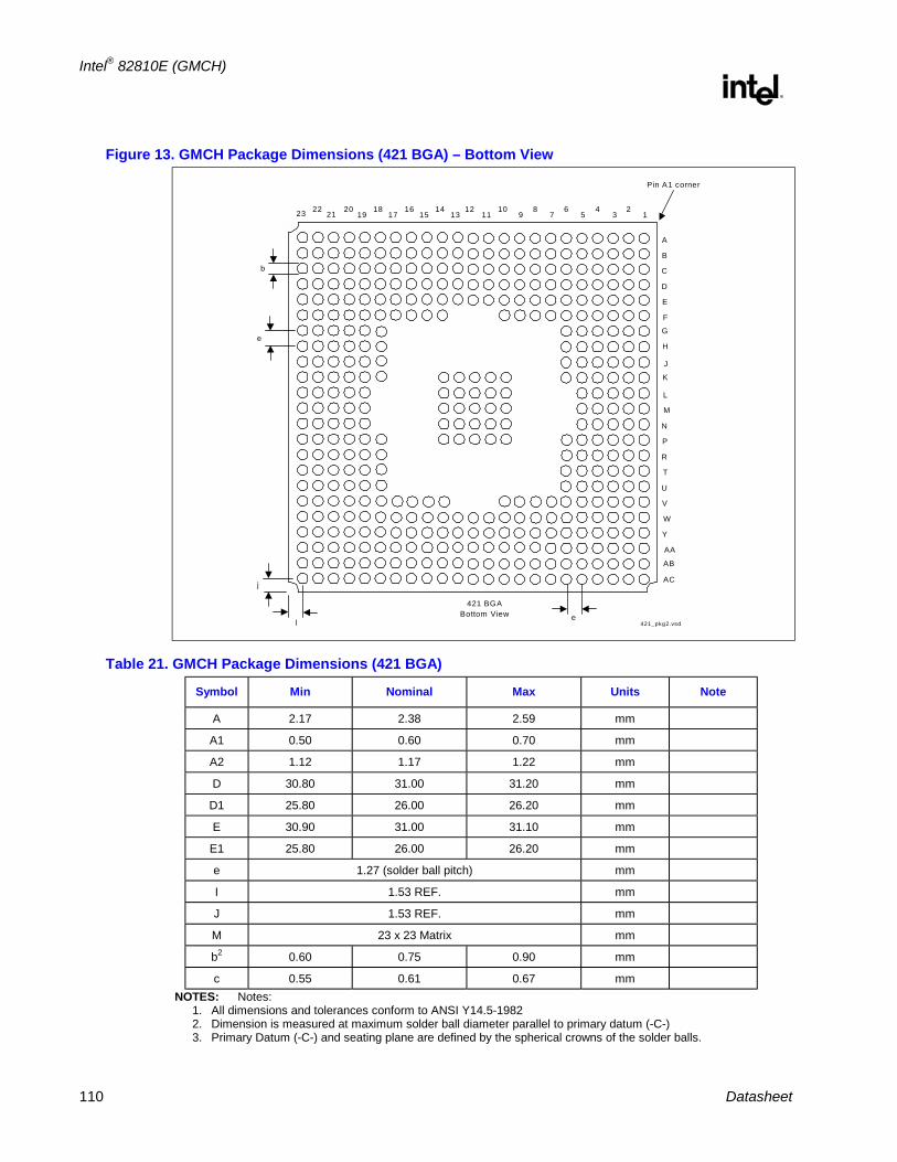
Intel® 82810E (GMCH)
R
110 Datasheet
Figure 13. GMCH Package Dimensions (421 BGA) – Bottom View
421_pkg2.vsd
Pin A1 corner
b
e
421 BGABottom View
j
l
21016202235791113151719 12123 4618 81214
A
B
C
D
E
F
G
H
J
K
L
P
R
T
U
V
Y
AB
AA
AC
N
W
M
e
Table 21. GMCH Package Dimensions (421 BGA)
Symbol Min Nominal Max Units Note
A 2.17 2.38 2.59 mm
A1 0.50 0.60 0.70 mm
A2 1.12 1.17 1.22 mm
D 30.80 31.00 31.20 mm
D1 25.80 26.00 26.20 mm
E 30.90 31.00 31.10 mm
E1 25.80 26.00 26.20 mm
e 1.27 (solder ball pitch) mm
I 1.53 REF. mm
J 1.53 REF. mm
M 23 x 23 Matrix mm
b2 0.60 0.75 0.90 mm
c 0.55 0.61 0.67 mm NOTES: Notes:
1. All dimensions and tolerances conform to ANSI Y14.5-1982 2. Dimension is measured at maximum solder ball diameter parallel to primary datum (-C-) 3. Primary Datum (-C-) and seating plane are defined by the spherical crowns of the solder balls.
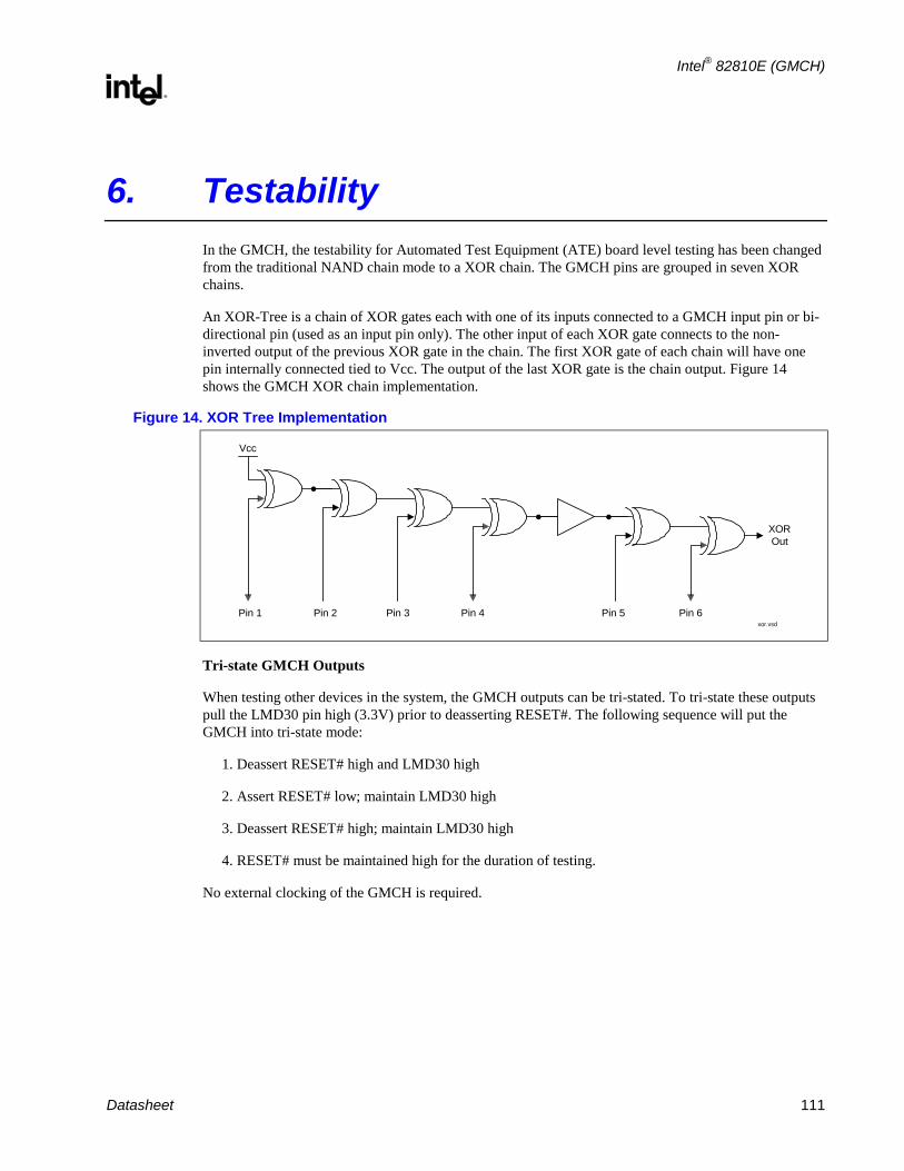
Intel® 82810E (GMCH)
R
Datasheet 111
6. Testability In the GMCH, the testability for Automated Test Equipment (ATE) board level testing has been changed from the traditional NAND chain mode to a XOR chain. The GMCH pins are grouped in seven XOR chains.
An XOR-Tree is a chain of XOR gates each with one of its inputs connected to a GMCH input pin or bi-directional pin (used as an input pin only). The other input of each XOR gate connects to the non-inverted output of the previous XOR gate in the chain. The first XOR gate of each chain will have one pin internally connected tied to Vcc. The output of the last XOR gate is the chain output. Figure 14 shows the GMCH XOR chain implementation.
Figure 14. XOR Tree Implementation
Vcc
Pin 1
XOROut
xor.vsdPin 2 Pin 3 Pin 4 Pin 5 Pin 6
Tri-state GMCH Outputs
When testing other devices in the system, the GMCH outputs can be tri-stated. To tri-state these outputs pull the LMD30 pin high (3.3V) prior to deasserting RESET#. The following sequence will put the GMCH into tri-state mode:
1. Deassert RESET# high and LMD30 high
2. Assert RESET# low; maintain LMD30 high
3. Deassert RESET# high; maintain LMD30 high
4. RESET# must be maintained high for the duration of testing.
No external clocking of the GMCH is required.

Intel® 82810E (GMCH)
R
112 Datasheet
6.1. XOR TREE Testability Algorithm Example XOR tree testing allows users to check, for example, opens and shorts to VCC or GND. An example algorithm to do this is shown in Table 22.
Table 22. XOR Test Pattern Example
Pin # from Figure 14
Vector PIN1 PIN2 PIN3 PIN4 PIN5 PIN6 XOROut
1 0 0 0 0 0 0 1
2 1 0 0 0 0 0 0
3 1 1 0 0 0 0 1
4 1 1 1 0 0 0 0
5 1 1 1 1 0 0 1
6 1 1 1 1 1 0 0
7 1 1 1 1 1 1 1
In this example, Vector 1 applies all “0s” to the chain inputs. The outputs being non-inverting, will consistently produce a “1” at the XOR chain output on a good board. One short to Vcc (or open floating to Vcc) will cause a “0” at the chain output, signaling a defect.
Likewise, applying Vector 7 (all “1”) to chain inputs (given that there are an even number of signals in the chain), will consistently produce a “1” at the XOR chain output on a good board. One short to Vss (or open floating to Vss) will cause a “0” at the chain output, signaling a defect. It is important to note that the number of inputs pulled to “1” will affect the expected chain output value. If the number chain inputs pulled to “1” is even, then expect “1” at XOR-out; otherwise, if odd, expect “0”.
Continuing to Illustrate with the example pattern in Table 22, as the pins are driven to “1” across the chain in sequence, XOR-out will toggle between “0” and “1”. Any break in the toggling sequence (e.g., “1011”) will identify the location of the short or open.
6.1.1. Test Pattern Consideration for XOR Chain 7
Bi-directional pins HLSTRB (chain 7) and HLSTRB# (chain 6) must always be complementary to each other. For example, if a “1” is driven on to HLSTRB, a “0” must be driven on HLSTRB# and vice versa. This will need to be considered in applying test patterns to this chain.

Intel® 82810E (GMCH)
R
Datasheet 113
6.2. XOR Tree Initialization
6.2.1. Chain [1:2, 4:7] Initialization
On chains [1:2,4:7], all that is required to prepare the device for XOR chain testing is to pull LMD31 high (+3.3V) prior to the deasserting RESET#. LMD31 must be brought back to a low state after this sequence, as this pin is part of XOR chain 2. The following sequence will put the GMCH into XOR testability mode:
1. Deassert RESET# high and LMD31 (high)
2. Assert RESET# low; maintain LMD31 (high)
3. Deassert RESET# high; maintain LMD31 (high)
4. RESET# must be maintained high for the duration of testing.
No external clocking of the GMCH is required for testing these chains.
6.2.2. Chain 3 Initialization
To test XOR chain 3, a different initialization sequence is required. The following steps need to be implemented:
1. Provide clocks at a minimum frequency of 10 MHz to the GMCH host clock (HCLK), hub interface clock (HLCLK), and display interface clock (DCLKREF). Phase relationship between HCLK and HLCLK must be maintained such that they are 180 degrees out of phase, and their edges line up within 400 pS.
2. Deassert RESET# high and assert LMD31 high
3. Assert RESET# low for 35,000 HLCLKs; maintain LMD31 high
4. Deassert RESET# high for 35,000 HLCLKs; maintain LMD31 high
5. Chain #3 is now initialized and ready to begin XOR test. RESET# must be maintained high for the duration of testing.
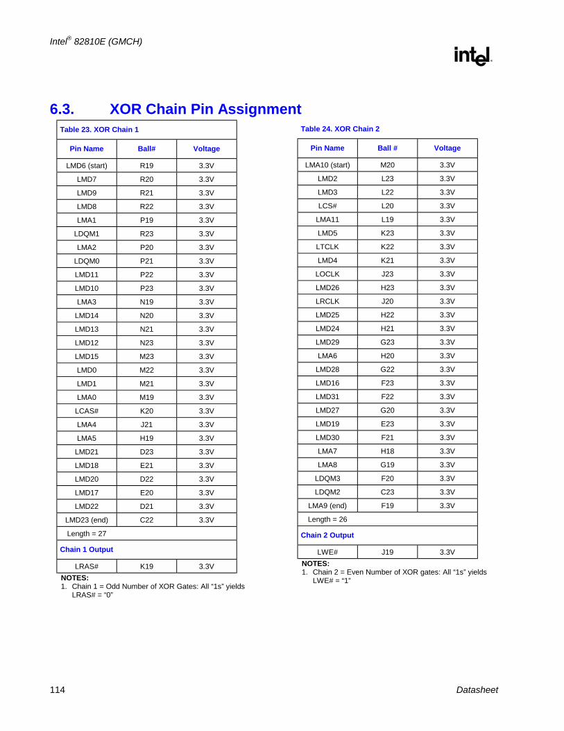
Intel® 82810E (GMCH)
R
114 Datasheet
6.3. XOR Chain Pin AssignmentTable 23. XOR Chain 1
Pin Name Ball# Voltage
LMD6 (start) R19 3.3V
LMD7 R20 3.3V
LMD9 R21 3.3V
LMD8 R22 3.3V
LMA1 P19 3.3V
LDQM1 R23 3.3V
LMA2 P20 3.3V
LDQM0 P21 3.3V
LMD11 P22 3.3V
LMD10 P23 3.3V
LMA3 N19 3.3V
LMD14 N20 3.3V
LMD13 N21 3.3V
LMD12 N23 3.3V
LMD15 M23 3.3V
LMD0 M22 3.3V
LMD1 M21 3.3V
LMA0 M19 3.3V
LCAS# K20 3.3V
LMA4 J21 3.3V
LMA5 H19 3.3V
LMD21 D23 3.3V
LMD18 E21 3.3V
LMD20 D22 3.3V
LMD17 E20 3.3V
LMD22 D21 3.3V
LMD23 (end) C22 3.3V
Length = 27
Chain 1 Output
LRAS# K19 3.3V NOTES: 1. Chain 1 = Odd Number of XOR Gates: All “1s” yields
LRAS# = “0”
Table 24. XOR Chain 2
Pin Name Ball # Voltage
LMA10 (start) M20 3.3V
LMD2 L23 3.3V
LMD3 L22 3.3V
LCS# L20 3.3V
LMA11 L19 3.3V
LMD5 K23 3.3V
LTCLK K22 3.3V
LMD4 K21 3.3V
LOCLK J23 3.3V
LMD26 H23 3.3V
LRCLK J20 3.3V
LMD25 H22 3.3V
LMD24 H21 3.3V
LMD29 G23 3.3V
LMA6 H20 3.3V
LMD28 G22 3.3V
LMD16 F23 3.3V
LMD31 F22 3.3V
LMD27 G20 3.3V
LMD19 E23 3.3V
LMD30 F21 3.3V
LMA7 H18 3.3V
LMA8 G19 3.3V
LDQM3 F20 3.3V
LDQM2 C23 3.3V
LMA9 (end) F19 3.3V
Length = 26
Chain 2 Output
LWE# J19 3.3V NOTES: 1. Chain 2 = Even Number of XOR gates: All “1s” yields
LWE# = “1”
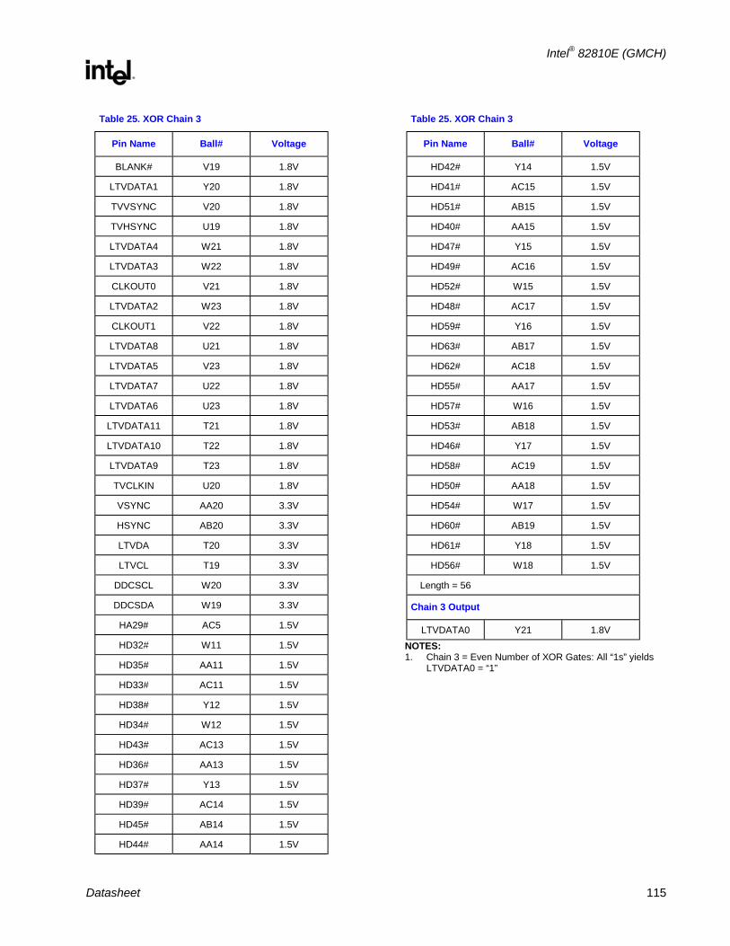
Intel® 82810E (GMCH)
R
Datasheet 115
Table 25. XOR Chain 3
Pin Name Ball# Voltage
BLANK# V19 1.8V
LTVDATA1 Y20 1.8V
TVVSYNC V20 1.8V
TVHSYNC U19 1.8V
LTVDATA4 W21 1.8V
LTVDATA3 W22 1.8V
CLKOUT0 V21 1.8V
LTVDATA2 W23 1.8V
CLKOUT1 V22 1.8V
LTVDATA8 U21 1.8V
LTVDATA5 V23 1.8V
LTVDATA7 U22 1.8V
LTVDATA6 U23 1.8V
LTVDATA11 T21 1.8V
LTVDATA10 T22 1.8V
LTVDATA9 T23 1.8V
TVCLKIN U20 1.8V
VSYNC AA20 3.3V
HSYNC AB20 3.3V
LTVDA T20 3.3V
LTVCL T19 3.3V
DDCSCL W20 3.3V
DDCSDA W19 3.3V
HA29# AC5 1.5V
HD32# W11 1.5V
HD35# AA11 1.5V
HD33# AC11 1.5V
HD38# Y12 1.5V
HD34# W12 1.5V
HD43# AC13 1.5V
HD36# AA13 1.5V
HD37# Y13 1.5V
HD39# AC14 1.5V
HD45# AB14 1.5V
HD44# AA14 1.5V
Table 25. XOR Chain 3
Pin Name Ball# Voltage
HD42# Y14 1.5V
HD41# AC15 1.5V
HD51# AB15 1.5V
HD40# AA15 1.5V
HD47# Y15 1.5V
HD49# AC16 1.5V
HD52# W15 1.5V
HD48# AC17 1.5V
HD59# Y16 1.5V
HD63# AB17 1.5V
HD62# AC18 1.5V
HD55# AA17 1.5V
HD57# W16 1.5V
HD53# AB18 1.5V
HD46# Y17 1.5V
HD58# AC19 1.5V
HD50# AA18 1.5V
HD54# W17 1.5V
HD60# AB19 1.5V
HD61# Y18 1.5V
HD56# W18 1.5V
Length = 56
Chain 3 Output
LTVDATA0 Y21 1.8V NOTES: 1. Chain 3 = Even Number of XOR Gates: All “1s” yields
LTVDATA0 = “1”

Intel® 82810E (GMCH)
R
116 Datasheet
Table 26. XOR Chain 4
Pin Name Ball# Voltage
HD27# (start) AB16 1.5V
HA14# T5 1.5V
HA16# V2 1.5V
HA11# U4 1.5V
HA10# W1 1.5V
HA3# U5 1.5V
HA15# W2 1.5V
HA28# Y1 1.5V
HA5# V4 1.5V
HA12# W3 1.5V
HA25# Y2 1.5V
HA21# AA1 1.5V
HD8# V5 1.5V
HA13# W4 1.5V
HA19# Y3 1.5V
HA18# AA2 1.5V
HA31# AB1 1.5V
HA24# AA3 1.5V
HA22# AB2 1.5V
HD1# W5 1.5V
HA30# Y4 1.5V
HA17# AC2 1.5V
HA20# AB3 1.5V
HD0# Y5 1.5V
HA23# AC3 1.5V
CPURST# AB4 1.5V
HD6# AA5 1.5V
HD5# Y6 1.5V
HA27# AC4 1.5V
HA26# AB5 1.5V
HD14# W7 1.5V
HD3# AA6 1.5V
HD18# Y7 1.5V
HD4# AB6 1.5V
HD2# W8 1.5V
Table 26. XOR Chain 4
Pin Name Ball# Voltage
HD12# AA7 1.5V
HD15# AC6 1.5V
HD10# AB7 1.5V
HD13# Y8 1.5V
HD9# AC7 1.5V
HD16# W9 1.5V
HD20# AB8 1.5V
HD30# Y9 1.5V
HD11# AC8 1.5V
HD7# AA9 1.5V
HD24# AB9 1.5V
HD17# AC9 1.5V
HD26# Y10 1.5V
HD19# AA10 1.5V
HD23# AB10 1.5V
HD21# AC10 1.5V
HD29# Y11 1.5V
HD25# AB11 1.5V
HD31# AC12 1.5V
HD28# AB12 1.5V
HD22# AB13 1.5V
Length =56
Chain 4 Output
SDQM3 D1 3.3V NOTES: 1. Chain 4 = Even Number of XOR Gates: All “1s” yields
SDQM3 = “1”

Intel® 82810E (GMCH)
R
Datasheet 117
Table 27. XOR Chain 5
Pin Name Ball# Voltage
SDQM1 (start) A10 3.3V
SDQM0 C10 3.3V
SMAA2 A9 3.3V
SMD45 E9 3.3V
SMD47 C8 3.3V
SMAA5 A8 3.3V
SMAA4 B8 3.3V
SMAB#7 A4 3.3V
SMAB#6 B4 3.3V
SCKE0 A3 3.3V
SCKE1 A2 3.3V
SMAA1 E7 3.3V
SMAA3 D7 3.3V
SMD46 E8 3.3V
SBS0 C5 3.3V
SMD56 F5 3.3V
SCS0# C4 3.3V
SMD57 G5 3.3V
SCSB1 C3 3.3V
SMD52 E4 3.3V
SMD20 D3 3.3V
SMD54 F4 3.3V
SMD53 E3 3.3V
SMD58 H5 3.3V
SDQM2 B1 3.3V
SMD18 G4 3.3V
SMD60 H6 3.3V
SMD48 F3 3.3V
SMD63 L5 3.3V
SMD29 L2 3.3V
SMD28 L1 3.3V
SMD30 M3 3.3V
DBSY# M4 1.5V
DRDY# N1 1.5V
RS2# N2 1.5V
Table 27. XOR Chain 5
Pin Name Ball# Voltage
ADS# N3 1.5V
HTRDY# N4 1.5V
RS0# N5 1.5V
HIT# P1 1.5V
RS1# P2 1.5V
HREQ2# P4 1.5V
HITM# R1 1.5V
HLOCK# P5 1.5V
HREQ3# R2 1.5V
DEFER# R3 1.5V
BPRI# T1 1.5V
HREQ0# R4 1.5V
HREQ1# T2 1.5V
HREQ4# R5 1.5V
BNR# T3 1.5V
HA4# U1 1.5V
HA7# T4 1.5V
HA8# U2 1.5V
HA6# V1 1.5V
HA9# U3 1.5V
Length = 55
Chain 5 Output
SMAA0 C9 3.3V NOTES: 1. Chain 5 = Odd Number of XOR Gates: All “1s” yields
SMAA0 = “0”
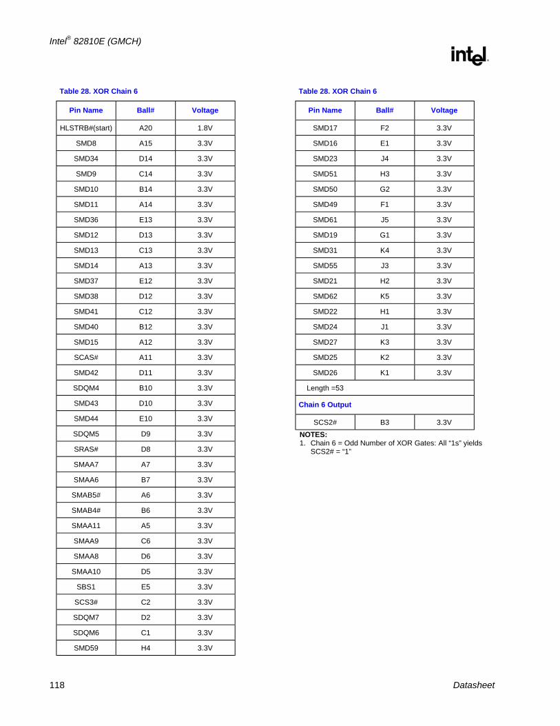
Intel® 82810E (GMCH)
R
118 Datasheet
Table 28. XOR Chain 6
Pin Name Ball# Voltage
HLSTRB#(start) A20 1.8V
SMD8 A15 3.3V
SMD34 D14 3.3V
SMD9 C14 3.3V
SMD10 B14 3.3V
SMD11 A14 3.3V
SMD36 E13 3.3V
SMD12 D13 3.3V
SMD13 C13 3.3V
SMD14 A13 3.3V
SMD37 E12 3.3V
SMD38 D12 3.3V
SMD41 C12 3.3V
SMD40 B12 3.3V
SMD15 A12 3.3V
SCAS# A11 3.3V
SMD42 D11 3.3V
SDQM4 B10 3.3V
SMD43 D10 3.3V
SMD44 E10 3.3V
SDQM5 D9 3.3V
SRAS# D8 3.3V
SMAA7 A7 3.3V
SMAA6 B7 3.3V
SMAB5# A6 3.3V
SMAB4# B6 3.3V
SMAA11 A5 3.3V
SMAA9 C6 3.3V
SMAA8 D6 3.3V
SMAA10 D5 3.3V
SBS1 E5 3.3V
SCS3# C2 3.3V
SDQM7 D2 3.3V
SDQM6 C1 3.3V
SMD59 H4 3.3V
Table 28. XOR Chain 6
Pin Name Ball# Voltage
SMD17 F2 3.3V
SMD16 E1 3.3V
SMD23 J4 3.3V
SMD51 H3 3.3V
SMD50 G2 3.3V
SMD49 F1 3.3V
SMD61 J5 3.3V
SMD19 G1 3.3V
SMD31 K4 3.3V
SMD55 J3 3.3V
SMD21 H2 3.3V
SMD62 K5 3.3V
SMD22 H1 3.3V
SMD24 J1 3.3V
SMD27 K3 3.3V
SMD25 K2 3.3V
SMD26 K1 3.3V
Length =53
Chain 6 Output
SCS2# B3 3.3V NOTES: 1. Chain 6 = Odd Number of XOR Gates: All “1s” yields
SCS2# = “1”
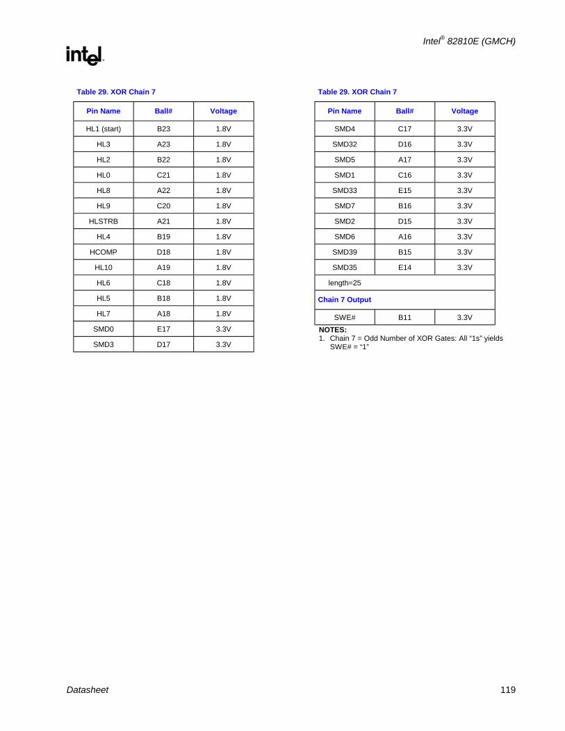
Intel® 82810E (GMCH)
R
Datasheet 119
Table 29. XOR Chain 7
Pin Name Ball# Voltage
HL1 (start) B23 1.8V
HL3 A23 1.8V
HL2 B22 1.8V
HL0 C21 1.8V
HL8 A22 1.8V
HL9 C20 1.8V
HLSTRB A21 1.8V
HL4 B19 1.8V
HCOMP D18 1.8V
HL10 A19 1.8V
HL6 C18 1.8V
HL5 B18 1.8V
HL7 A18 1.8V
SMD0 E17 3.3V
SMD3 D17 3.3V
Table 29. XOR Chain 7
Pin Name Ball# Voltage
SMD4 C17 3.3V
SMD32 D16 3.3V
SMD5 A17 3.3V
SMD1 C16 3.3V
SMD33 E15 3.3V
SMD7 B16 3.3V
SMD2 D15 3.3V
SMD6 A16 3.3V
SMD39 B15 3.3V
SMD35 E14 3.3V
length=25
Chain 7 Output
SWE# B11 3.3V NOTES: 1. Chain 7 = Odd Number of XOR Gates: All “1s” yields
SWE# = “1”
Top Related