


Languages
Pages
Legal


Digital Logic and Design (Course Code: EE222)
Lecture 24: FSM Design, Sequential Circuits Contd..
Course Instructor: Shree Prakash Tiwari
Email: [email protected]
Webpage: http://home.iitj.ac.in/~sptiwari/ Course related documents will be uploaded on
http://home.iitj.ac.in/~sptiwari/DLD/
Indian Institute of Technology Jodhpur, Year 2018-2019
1
Note: The information provided in the slides are taken form text books Digital Electronics (including Mano & Ciletti), and various other resources from internet, for teaching/academic use only

Overview
° Design of systems that input flip flops and combinational logic
° Specifications start with a word description ° Create a state table to indicate next states ° Convert next states and outputs to output and flip flop
input equations • Reduce logic expressions using truth tables
° Draw resulting circuits.
Lots of opportunities for interesting design

Designing Finite State Machines
° Specify the problem with words ° (e.g. Design a circuit that detects three
consecutive 1 inputs) ° Assign binary values to states ° Develop a state table ° Use K-maps to simplify expressions
° Flip flop input equations and output equations ° Create appropriate logic diagram
° Should include combinational logic and flip flops

FSM Design
Example:
Design a FSM that detects a sequence of three or
more consecutive ones on an input bit stream.
The FSM should output a 1 when the sequence is detected, and a 0 otherwise.
A circuit that detects the occurrence of a particular pattern on its input is referred to as a sequence detector.

FSM Design: Example
Input: 0 1 1 1 0 1 0 1 1 0 1 1 1 0 1 … Output: 0 0 0 1 0 0 0 0 0 0 0 0 1 0 0 …
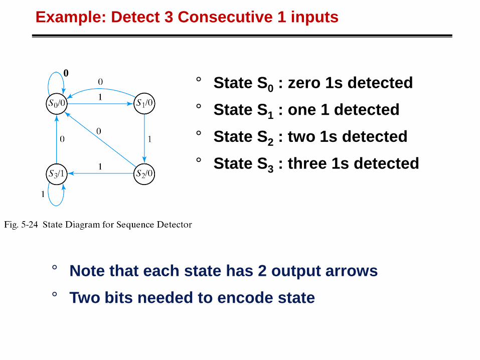
Example: Detect 3 Consecutive 1 inputs
° State S0 : zero 1s detected ° State S1 : one 1 detected ° State S2 : two 1s detected ° State S3 : three 1s detected
0
° Note that each state has 2 output arrows ° Two bits needed to encode state

State Table for Sequence Detector
° Sequence of outputs, inputs, and flip flop states enumerated in state table
° Present state indicates current value of flip flops
° Next state indicates state after next rising clock edge
° Output is output value on current clock edge
Present State
Next State
A B x A B y 0 0 0 0 0 0 0 0 1 0 1 0 0 1 0 0 0 0 0 1 1 1 0 0 1 0 0 0 0 0 1 0 1 1 1 0 1 1 0 0 0 1 1 1 1 1 1 1
Output Input
° S0 = 00 ° S1 = 01
° S2 = 10 ° S3 = 11

State Table for Sequence Detector
° S0 = 00 ° S1 = 01
° S2 = 10 ° S3 = 11
QA QB QA+ QB
+
Q+ = D next state flip-flop input

FSM Design: Example (Moore)
The choice of Flip-Flop determines the complexity of the combinational logic required in the design of the state machine.
Each type of Flip-Flop has a unique characteristic equation.
SR Flip-Flop − Q+ = S + R'.Q
D Flip-Flop − Q+ = D
JK Flip-Flop − Q+ = J.Q' + K'.Q
T Flip-Flop − Q+ = T '.Q + T.Q'

Finding Expressions for Next State and Output Value
° Create K-map directly from state table (3 columns = 3 K-maps) ° Minimize K-maps to find SOP representations ° Separate circuit for each next state and output value
Q+ = D next state flip-flop input

Circuit for Consecutive 1s Detector
° Note location of state flip flops
° Output value (y) is function of state
° This is a Moore machine.
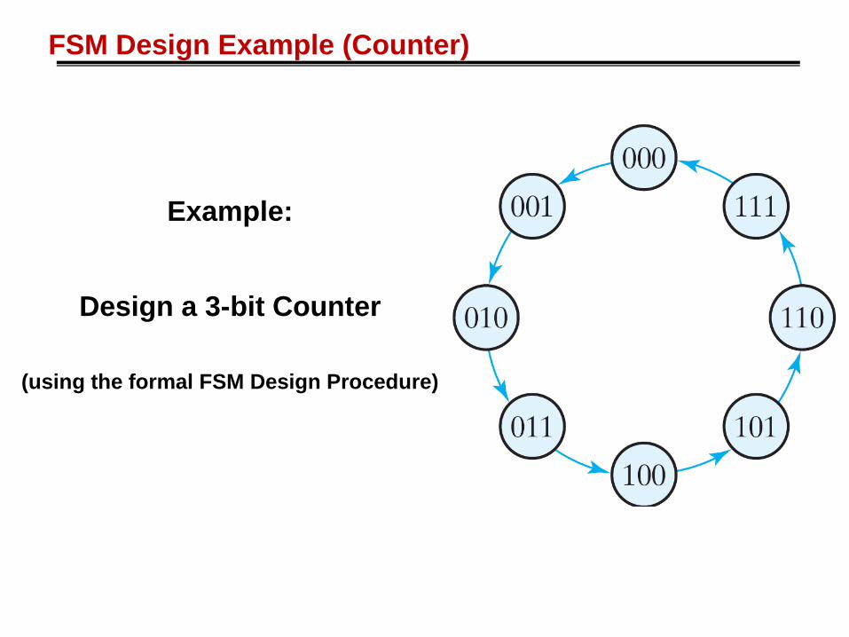
FSM Design Example (Counter)
Example:
Design a 3-bit Counter
(using the formal FSM Design Procedure)

FSM Design: Example
What is the output of a counter?
Synthesis using T Flip-Flops
(Q+ = T'.Q + T.Q')
+
Excitation Table

FSM Design: Example
Q+ = T.Q' + T'.Q next state
flip-flop input

FSM Design: Example

What next……
° Sequential Circuits contd…

Assignment: Design a Mod-5 synchronous counter using JK flip-flops using step by step FSM design procedure. Solve as discussed in the class, and submit the assignment in next class…
Example

Concept of the State Machine
Example: Odd Parity Checker
Even [0]
Odd [1]
Reset
0
0
1 1
Assert output whenever input bit stream has odd # of 1's
State Diagram
Present State Even Even Odd Odd
Input 0 1 0 1
Next State Even Odd Odd Even
Output 0 0 1 1
Symbolic State Transition Table
Output 0 0 1 1
Next State 0 1 1 0
Input 0 1 0 1
Present State 0 0 1 1
Encoded State Transition Table
° Note: Present state and output are the same value ° Moore machine

Concept of the State Machine
Example: Odd Parity Checker
Next State/Output Functions NS = PS xor PI; OUT = PS
D
R
Q
Q
Input
CLK PS/Output
\Reset
NS
D FF Implementation
Timing Behavior: Input 1 0 0 1 1 0 1 0 1 1 1 0
Clk
Output
Input 1 0 0 1 1 0 1 0 1 1 1 0
1 1 0 1 0 0 1 1 0 1 1 1

Mealy and Moore Machines
Solution 1: (Mealy)
0/0
Even
Odd
1/1 1/0
0/1
0 Even
1 1
0
Reset [0]
Odd [1]
Output
Input
Output
Input
Transition Arc
Output is dependent only on current state
O/P is dependent on current state and input in Mealy
Solution 2: (Moore)
Mealy Machine: Output is associated with the state transition - Appears before the state transition is completed (by the next clock pulse).
Moore Machine: Output is associated with the state -Appears after the state transition takes place.

Vending Machine FSM
Step 1. Specify the problem
Vending Machine
FSM
N
D
Reset
Clk
OpenCoin
Sensor Gum Release
Mechanism
Deliver package of gum after 15 cents deposited Single coin slot for dimes (10 cents), nickels (5 cents)
No change
Design the FSM using combinational logic and flip flops

Vending Machine FSM
State Diagram
Reset
N
N
N, D
[open]
15¢
0¢
5¢
10¢
D
D
Reuse states whenever possible Symbolic State Table
Present State
0¢
5¢
10¢
15¢
D 0 0 1 1 0 0 1 1 0 0 1 1 X
N 0 1 0 1 0 1 0 1 0 1 0 1 X
Inputs Next State
0¢ 5¢ 10¢ X 5¢ 10¢ 15¢ X
10¢ 15¢ 15¢ X
15¢
Output Open
0 0 0 X 0 0 0 X 0 0 0 X 1

Vending Machine FSM
State Encoding
Next State D 1 D 0 0 0 0 1 1 0 X X 0 1 1 0 1 1 X X 1 0 1 1 1 1 X X 1 1 1 1 1 1 X X
Present State Q 1 Q 0 0 0
0 1
1 0
1 1
D 0 0 1 1 0 0 1 1 0 0 1 1 0 0 1 1
N 0 1 0 1 0 1 0 1 0 1 0 1 0 1 0 1
Inputs Output Open
0 0 0 X 0 0 0 X 0 0 0 X 1 1 1 X
How many flip-flops are needed?

Vending Machine FSM
Determine F/F implementation
K-map for Open K-map for D0
K-map for D1
Q1 Q0 D N
Q1
Q0
D N
Q1 Q0 D N
Q1
Q0
D N
Q1 Q0 D N
Q1
Q0
D N

D Q
Q R
D Q
Q R
Q0
N
N
Q0
Q1 N
Q1 D
D0
D1 Q1
OPEN
D
0Q
NCLK
CLK
Vending machine FSM implementation based on D flip-flops(Moore).
0Q
1Q
Q1
Q0
Reset
Reset
Minimized Implementation

Summary
° Finite state machines form the basis of many digital systems
° Designs often start from clear specifications ° Develop state diagram and state table ° Optimize using combinational design techniques ° Mealy or Moore implementations possible
• Can model approach using HDL.
Top Related