


Languages
Pages
Legal

HORIZON RAMDISX
CONSTRUCTION GUIDE
bU
Ron Griefs
COPYRIGHT 1906, Horizon Computer, Limited
,B ALL RIGHTS RESERVED

TABLE OF CONTENTS
INTRODUCTION 1
COMPATIBILITY 1
INSTALLATION INSTRUCTIONS 2
r, Unpacking the Card
Determining CRU Base Address Installing the Card 4
Loading the RAMDISK Operating System 4
Loading DM-1000 Disk Manager I-
CALL SUBPROGRAM': 7
CALL DN(n) Set Drive Number CALL MS(n) .Set Max. Sectors
q
9 CALL WO Turn On Write Protect CALL WF Turn Off Write Protect 9
CALL EX(a) Execute Machine Language 9
CALL CO Enable DSR RAM 10 CALL CF Turn Off DSR RAM 10 CALL DM Load DM-1000 from RAMDISK 10 CALL NF(n) Set Number of Floppy Drives 10
DELETE "XBCALL" Download Ext. BASIC Routines 11
COMMON RAMDISK APPLICATIONS 12
TI Writer / TK Writer 1? Ti Multiplan 1. TI BASIC and TI Extended BAbir 13 Editor/Assembler 13
IN CASE OF DIFFICULTY 14
Testing for Repeatability 14 RAMDISK as Cause 14 Testing the Memory with MEMTEST- 15 Inability to Access Floppies ff. Lock—up on Power—Up lb
ADVANCED APPLICATIONS • 1 ,
Introduction 12 Card Architecture 1P How to Enable the Memory 20 Loading Your Own Programs 21
Experimenting with D'SR'= 23 Writing CALL Subprograms 23.
Disk Contents .7,p
RAMDIF.K CONSTRUCTION GUIDE 30
Introduction 31 Eight Construction Steps 72 Schematic and Parts List -2..7,

EXCLUSION OF WARRANTIES
The information contained in this manual is subject to
change without notice. Horizon Computer, Limited shall
not be liable for technical or editorial errors or
omissions contained herein; nor for incidental or consequential damages resulting from the furnishing, performance, or use of this material or product described by this material.
Horizon Computer, Limited makes no warranty, expressed
or implied, including but not limited to implied war-
ranties of merchantability and fitness for a particular purpose. All software, hardware, and printed materi als are made available solely on an AS IS basis.
THE USER ASSUMES SOLE RESPONSIBILITY FOR DETERMINATION
OF FITNESS OF THIS PRODUCT FOR A PARTICULAR APPLICATION.
LIMITED THREE MONTH WARRANTY
Her Computer, Limited warrants its fully built and
tested RANDISK to be free from defects in materials
and workmanship for a period of three months from the original date of purchase. This warranty shall extend only to the original consumer purchaser. This warranty
is void if the RAMDISK has been damaged by accident, unreasonable use, nerilect, improper service, or other
cause not arising out of defects in materials or
workmanship.
No warranty is made for products other than completed
RAMDISKs, including printed circuit boards. and other
parts, software programs, and printed materials.
Horizon Computer, Limited shall riot be liable for loss of use of the RAMDISK or other incidental or conse-
quential damages incurred by the consumer or any other
user. In any case, Horizon Computer, Limited shall be
liA.blP only for the cost of the RAMDISK arid associated materials.
Users Manual by D. R. Romer
Construction Guide by R. dries ROS modifications by J. Peter Hoddie
COPYRIGHT 1986, Horizon Computer, Limited
ALL RIGHTS RESERVED
- 1 - INTRODUCTION
The HORIZON RAMDISK is a peripheral card for the
TI-99/4A Home Computer. The RAMDISK is a battery-backed,
solid state device which is intended to emulate all functions
of a TI floppy disk drive. The primary advantage of the
RAMDISK is speed; data transfer takes place roughly twenty
times faster.
To use the HORIZON RAMDISK you need:
1) TI-99/4A console and TV or monitor
2) 99/4 Peripheral Expansion Box
3) TI Compatible Disk Controller Card
4) At least one floppy disk drive
5) One of the following Command Modules
A) TI Extended BASIC
B) Editor/Assembler
C) TI-Writer
S) 32K Memory Expansion (recommended)
COMPATIBILITY
Every attempt has been made to insure that the HORIZON
RAMDISK will be compatible with TI and third party software.
The RAMDISK appears to be compatible with TI Wr i ter,
Editor/Assembler, Multiplan, Logo, Forth, BASIC, Extended
BASIC and Assembly Language. Most applications concerning
the above should be compatible with the RAMDISK. However,
some software, designed to directly access the Disk
Controller Card will not recognize the RAMDISK and hence is
not compatible. Examples include the CorComp Disk Manager
Program and TI Pascal. Non-standard disk access techniques
or disk protection schemes could also cause compatibility
problems (e.g., TI-ARTIST).

- 2 -
HORIZON RAMDISK
INSTALLATION INSTRUCTIONS
Horizon Computer, Limited
*******************************************
CAUTION: Your HORIZON RAMDISK contains
components which can be damaged by•
STATIC ELECTRICITY. Please follow the
instructions below CAREFULLY!
*******************************************
1) UNPACKING .THE CARD
BEFORE UNPACKING YOUR•CARD... you should know it
contains CMOS RAM "chips" which are damaged by STATIC
ELECTRICITY MORE EASILY•THAN OTHER LOGIC TYPES. Therefore, you should take proper precautions in handling the card as
described below. THIS IS ESPECIALLY TRUE IN LOW HUMIDITY ENVIRONMENTS -- REMEMBER THAT WINTER PRODUCES IDEAL CONDITIONS FOR STATIC!
Most people are aware of the kinds of things that
produce static charges -- synthetic garments, carpeting,
plastics (not specially treated), etc. When handling the
card, please use common sense and AVOID CONDITIONS WHICH
MIGHT PRODUCE STATIC CHARGES.
Your card has been packaged in a pink static protective
bag. Save this bag and use it when you transport the card or if you have to send it back for service.
Before unpacking the card, take appropriate precaution=, to prevent static charges. Then make sure you ground
yourself by touching a metal object the INSIDE METAL structure of your Peripheral Expansion Box is ideal. When handling, try to touch ONLY the edges of the card, and DO NOT
touch the CMOS memory chips themselves -- they are the larger
devices which occupy most of the board.
2) DETERMINING THE CRU BASE ADDRESS
Your HORIZON RAMDISK has been provided with a DIP (Dual In-line Package) switch for setting.the
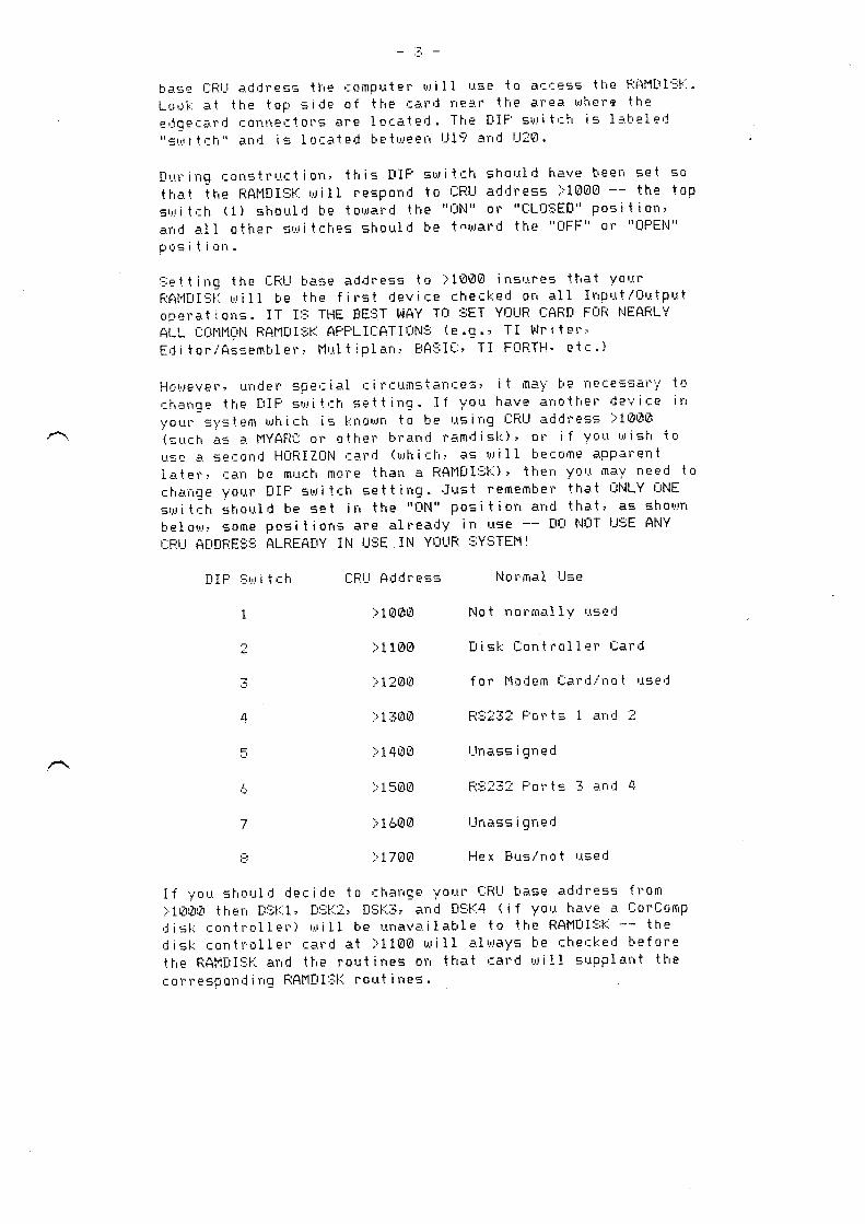
base CRU address the computer will use to access the RAMDISK. Look at the top side of the card near the area where the
edgecard connectors are located. The DIP switch is labeled
"switch" and is located between 1119 and U20.
During construction, this DIP switch should have been set so
that the RAMDISK will respond to CRU address >1000 -- the top
switch (1) should be toward the "ON" or "CLOSED" position,
and all other switches should be toward the "OFF" or "OPEN"
position.
Setting the CRU base address to >1000 insures that your RAMDISK will be the first device checked on all Input /Output operations. IT IS THE BEST WAY TO SET YOUR CARD FOR NEARLY ALL COMMON RAMDISK APPLICATIONS (e.g., TI Writer,
Editor/Assembler, Multiplan, BASIC, TI FORTH, etc.)
However, under special circumstances, it may be necessary to
change the DIP switch setting. If you have another device in
your system which is known to be using CRU address >1000
(such as a MYARS or other brand ramdisk), or if you wish to use a second HORIZON card (wh i ch, as will become apparent
later, can be much more than a RAMDISK), then you may need to
change your DIP switch setting. Just remember that ONLY ONE
switch should be set in the "ON" position and that as shown
below, some positions are already in use -- DO NOT USE ANY
CRU ADDRESS ALREADY IN USE .IN YOUR SYSTEM!
DIP Switch CRU Address Normal Use
1 >1000 Not normally used
.7) >1100 Disk Controller Card
--.., >1200 for Modem Card/riot used
4 >1300 RS232 Forts 1 and 2
5 >1400 Unassigned
6 >1500 RS232 Ports 3 and 4
7 >1600 Unassigned
>1700 Hex Bus/not used
If you should decide to change your CRU base address from
>1000 then DSK1, DSK2, DSK3, and DSK4 (if you have a CorComp disk controller) will be unavailable to the RAMDISK -- the
disk controller card at >1100 will always be checked before
the RAMDISK and the routines on that card will supplant the
corresponding RAMDISK routines.

So, in summary, we recommend that unless you have A strong
reason to change it, leave EIP switch 1 "ON" so the CRU base
address of the card will be >1000.
3) INSTALLING THE CARD
*********************************************
CAUTION: As with ALL Peripheral Expansion :
Box (PEB) cards, you MUST turn OFF PE—Box
power and wait a FULL TWO MINUTES before :4:
installing or removing the RAMDISK card.
*********************************************
After removing the card from the packaging material look for the red LED (Light Emitting Diode) nearest one CORNER of the
board. To orient the card correctly for installation, this LED must point toward the FRONT of the Peripheral Expansion
Box. When the card is properly oriented, all of the IC's and
other components will be facing the disk drive enclosure.
Install the card in any available slot -- just make sure that none of the components on either side of the card contact the
"clam—shell" case of an adjacent card. This will avoid a
Short circuit.
4) LOADING THE RAMDISK OPERATING SYSTEM
Your System Master diskette contains all of the programs
required to load the RAMDISK operating system. It is -
recommended that you make a back—up copy and keep the System
Master diskette in a safe place.
The System Master diskette contains a program called UTILl.
This is an assembly language loader program for the RAMDISK operating system. It requires one of the following modules to execute: Extended Basic, Editor/Assembler or TI—Writer.
If Extended Basic is used the files LOAD and YLOAD are also
required.
The operating system is contained in two files called PARTA_04 and PARTB04. These files MUST BE PRESENT ON A
DISKETTE WITH THE NAME ROS so the UTIL1 program can find
them. (That is why the System Master diskette is named PUS
ROS is an acronym for Ram Operating System. NEVER NAME
THE RAMDISK ROS!)
The diskette, named ROS containing the above files may be placed in any drive EXCEPT DRIVE 3 (upon loading the
operating system the RAMDISK becomes drive 3.) If using
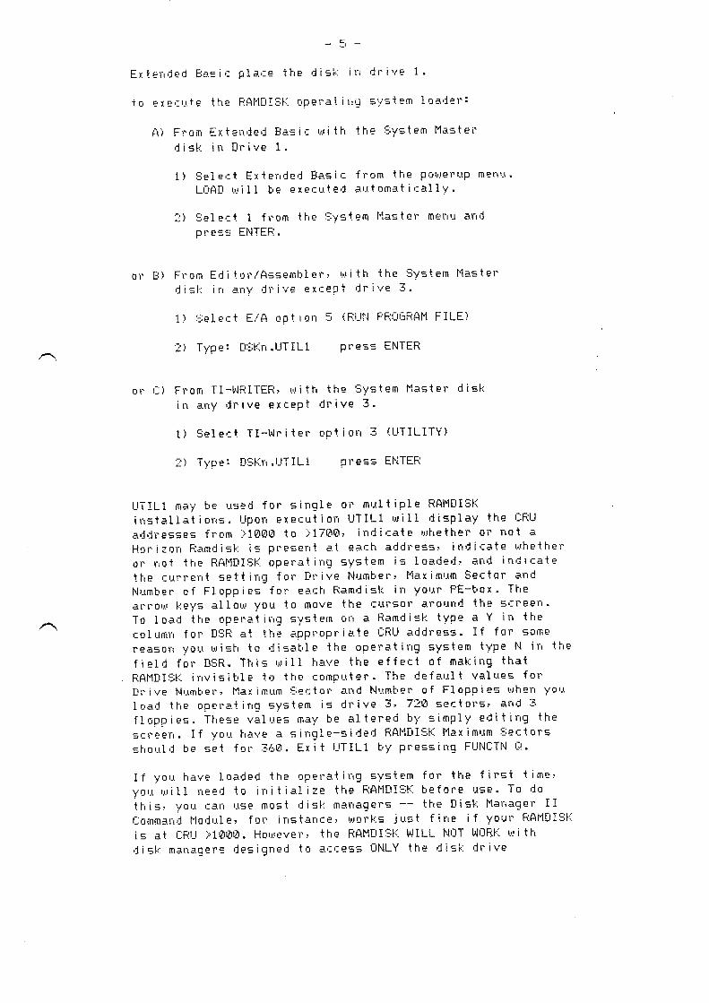
5
Extended Basic place the disk in drive 1.
to exPcute the RAMDISK operating system loader:
A) From Extended Basic with the System Master
disk in Drive 1.
1) Select Extended Basic from the powerup menu. LOAD will be executed automatically.
2) Select 1 from the System Master menu and
press ENTER.
or B) From Editor/Assembler, with the System Master
disk in any drive except drive 3.
1) Select E/A option 5 (RUM PROGRAM FILE)
2) Type: DSKn.UTIL1 press ENTER
or C) From TI-WRITER, with the System Master disk
in any drive except drive 3.
1) Select TI-Writer option 3 (UTILITY)
2) Type: DSKn.UTII 1 press ENTER
UTIL1 may be used for single or multiple RAMDISK installations. Upon execution UTIL1 will display the CRU
addresses from >1000 to >1700, indicate whether or riot a
Horizon Ramdisk is present at each address, indicate whether
or not the RAMDISK operating system is loaded, and indicate
the current setting for Drive Number, Maximum Sector and Number of Floppies for each Ramdisk in your PE-box. The arrow keys allow you to move the cursor around the screen.
To load the operating system on a Ramdisk type a Y in the
column for DSR at the appropriate CRU address. If for some
reason you wish to disable the operating system type N in the
field for DSR. This will have the effect of making that
RAMDISK invisible to the computer. The default values for Drive Number, Maximum Sector and Number of Floppies when you load the operating system is drive 3, 720 sectors, and 3
floppies. These values may be altered by simply editing the
screen. If you have a single-sided RAMDISK Maximum Sectors
should be set for 360. Exit UTIL1 by pressing FUNCTN Q.
If you have loaded the operating system for the first time,
you will need to initialize the RAMDISK before use. To do
this, you can use most disk managers -- the Disk Manager II
Command Module, for instance, works just fine if your RAMDISK
is at CPU >1000. However, the RAMDISK WILL NOT WORK with
disk managers designed to access ONLY the disk drive

— 6 —
controller card (such as the CorComp Disk Manager -- the
CorComp Disk Manager Program will not recognize the HORIZON
RAMDISK).
By special agreement with the Ottawa. TI 97/4 Users Group,
your System Master diskette also contains Version 3.3 of Disk
Manager 1000 (DM-1000) written by Bruce Caron and revised by
Ralph Romans. Documentation for DM-1000 is files DMDOCPT1 to
4 on the disk named SOURCE—B. The documentation files may be
read with TI—Writer or printed. It is an excellent disk
manager and as will be explained more fully later, can be loaded directly from BASIC or Extended BASIC with your
HORIZON RAMDISK.
The first time you load DM-1000, follow this procedure.
A) From Extended Basic with the System Master
disk in drive 1...
1) Select Extended Basic from the powerup menu.
LOAD will be executed automatically.
2) Select 2 from the'System Master menu and
press ENTER.
or B) From Editor/Assembler with the System Master disk in any drive except drive 3...
1) Select E/A option 5 (RUN PROGRAM FILE)
2) Type: DSKn.MGR1 press ENTER
or C:) From TI—Writer with the System Master disk in
any drive except drive 3...
1) Select TI—Writer option 3 (UTILITY).
2) Type: DSKn.MGR1 press ENTER
You should now see the DM-101710 master screen -- if ynu're at
all familiar with the CorComp disk manager, you'll find
DM-1000 very easy to use. Otherwise, PLEASE READ THE DOCUMENTATION FILES.
With DM-1000 loaded, you need to initialize your RAMDISK;
keeping in mind the values set for drive number and Maximum
Sectors when you loaded the operating system. If you have a
single—sided RAMDISK, change the maximum number of sectors with CALL MSS (360) from BASIC as described below before
initializing.
- ;7 -
After initializing your RAMDISK, use DM-1000's File Copy utility to copy two files from the System Master disk to the
RAMDISK These two MGR1 and MGR2, contain the DM-1000
prooram. To leave DM-1000, use FCTN QUIT.
Once you have completed all of the above steps, you are ready
to proceed with the remainder of the RAMDISK reference manual.

CALL SUBPROGRAMS AVAILABLE ON THE HORIZON RAMDISK
The RAMDISK contains nine CALL subprograms which you cart use directly from TI BASIC or TI Extended BASIC. (Access
from a running Extended program is effected using the special
statement DELETE XBCALL as described below.) These subprograms can be used either within programs or in Command Mode.
1) CALL DN(n) — CHANGE RAMDISK DRIVE NUMBER
Whenever the RAMDISK operating system is installed, the
RAMDISK will automatically respond as drive 3; i.e., to DSK3
access. However, with the CALL DN(n) statement you can
change the number the RAMDISK responds to, and because it is
battery—backed, it will respond to this number until changed
with another CALL DN(n) statement. The "n" inside the
parentheses MUST BE A ::;ING1 F DIGIT FROM 1 TO A. <Variable
names are riot allowed.) When the CALL DN(n) statement is
executed, the RAMDISK will respond to any standard disk
access to that drive number (DSKn.XYZ).
There are a few restrictions, however. First, no files
can be OPEN in either the drive number currently assigned to
the RAMDISK or the drive number to which the RAMDISK will be
changed. For example:
A) If the RAMDISK were set to respond to DSK3;
B) You had a file OPEN on a diskette in DSK1; and
C) You then tried CALL DN(1) -- which would make
the RAMDISK respond to any drive 1 access -- you
would receive an INCORRECT STATEMENT error message
because of the OPEN file on drive 1.
However, if you first CLOSE the file i rt drive 1, then
CALL DN(1) will work (assuming no files are OPEN for drive 3,
of course).
Remember, CALL subprograms can be used within a TI BASIC program; so if you encounter an INCORRECT STATEMENT error in
a. program which uses CALL DN(n) statements, check to make sure all files are CLOSED for both the drive number the RAMDISK was and the one it will be
The second thing to be aware of involves what happens to "real" disk drive units normally assigned the number being
used by the RAMDISK -- they cannot be accessed except by disk
name. If for example, you use a CALL DN(2) then all DSK2
access will reference the RAMDISK -- if you have a disk drive
2 attached to your system, it will become "invisible" until
the RAMDISK drive number is changed.However, you can use the disk name option -- DSK.DISKNAME.FILENAME -- to access the disk drive which has the same number as the RAMDISK.
(Another exception to the above is use of the CorComp Disk Manager and other programs that do riot recognize the
RAMDISK.)

- 9 -
2) CALL MS (n) - CHANGE MAXIMUM NUMBER OF SECTORS
This subprogram sets an upper limit on the number of sectors
the operating system will recognize as valid. If you try to
access a sector above this number (as in initialization of a
disk) an error condition will occur. Once set, the number
will remain in effect even after the system has been
powered-down because the RAMDISK is battery-backed.
Your RAMDISK may vary with respect to the number of "sectors" of RAM actually on it. In general, if you have a
"single-sided" RAMDISK, the maximum number of sectors is 360
and if it's double-sided the maximum is 720. NEVER SET THE NUMBER OF SECTORS HIGHER THAN THE ACTUAL AVAILABLE SPACE ON YOUR RAMDISK.
The CALL MS(n) statement allows you to inform the operating
system as to how many sectors are available for use. Again,
"n" must be a group of DIGITS -- not a variable name. For a
single-sided RAMDISK, you would enter CALL MS(360) and for a
double-sided one CALL MS(720).
When the operating system is loaded, it will automatically
enter a default value of 720. If you have a double-sided
RAMDISK, you can initialize it as double sided right away.
Similarly, if you have a single-sided RAMDISK you may
initialize it as single sided with no problem, but to avoid confusion it is a good idea to set the number of sectors at
340 before initializing.
3) CALL WE' / WF - TURN DISK WRITE-PROTECT ON AND OFF
By entering CALL WO (write protect on) from BASIC you have,
in effect, write protected the entire disk (this is much like putting a write-protect tab on a Ojskette). Similarly, by
entering CALL WO from BASIC, you have removed the disk write
protectiOn. At the time the operating system is loaded, disk write-protection is "OFF".
Remember, the RAMDISK is battery-backed. If you write
protect the RAMDISK today, it will still be write protected
when you turn on your system tomorrow.
4) CALL EX(adr) -•EXECUTE MACHINE CODE
This subprogram allows the user to transfer control of a BASIC or Ext. BASIC program to a specified address within
the computer's CPU memory. The address must be DIGITS --
variable names are not allowed. All values are in decimal
using the same conventions as TI's CALL LOAD subprogram. Since the power-up routine starts at >0024, it may be
executed with the statement: CALL EX(36), for instance.

- 10. -
5) CALL CO / CF - TURN DSRam ON AND OFF
The CALL CO (card or,) instruction enables the RAMDISK operating system. You will see the red LED light. At the same time it allows you direct access to 6K of the operating system software (from >4000 to >57FF) and the first eight sectors of the RAMDISK (>5800 to >5FFF). This information can be accessed directly from BASIC using the CALL LOAD and CALL PEEK subprograms in many modules. But even more importantly, in connection with the CALL EX subprogram (described as (4) above), you can directly link to operatinci system software from TI BASIC.
Before practical use can be made of this subprogram with respect to RAMDISK software, you will need the operating system source code and other information supplied with the RAMDISK. The CALL CO and CALL CF subprograms are described for those experimenters who will choose to do some work outside the RAMDISK environment as described in the "Advanced" section of this manual.
The CALL CF subprogram just shuts the card off, and of course the LED goes off.
6) CALL DM - LOAD DM-1000
This subprogram loads the DM-1000 disk manager from the RAMDISK if the RAMDISK contains the two files MGR1 and MGR?. If you have these two files on your RAMDISK, DM-1000 will Load (rapidly, of•course) arid• if you do riot have the two files on your RAMDISK, the subprogram should act like a REM statement -- nothing will happen.
DM-1000 turns on drive 1 after it is loaded to look for a configuration file. This slows things down by a second or so. So if you want really fast access to DM-1000, make your RAMDISK DSK1 (using the CALL DN(n) subprogram described above.)
7) CALL NF (n) - SET NUMBER OF FLOPPY DRIVES
If the base CPU address is set at the normal value of •1000, then the CALL NF-statement is of no use.
When the RAMDISK base CRU address is not >1000, a special quantity must be specified if DM-1000 is to access the RAMDISK. This value is set equal to the number of actual floppy drives attached to the user's system. If the RAMDISK drive number is set greater than this value, then DM-1000 will be able to ;Access it.
If the CPU base is not >1000, then BASIC: and other programs accessing disk drives can access the RAMDISK only when its number is greater than the MAXIMUM number of drives the disk drive controller can access (3 for TI controller and 4 for CorComp). However, by proper specification of NF, DM-1000 can access the RAMDISK at an/ number from 2 to 6.

When the Operating System is loaded, NF has the value of 3.
In the CNL NF(n) statement, (n) is a digit between 1 and 5.
Variable names are not allowed.
8) DELETE "XBCALL" - DOWNLOAD MACHINE LANGUAGE FOR XB LINKS
The CALL statements as described above will not execute from a running Extended BASIC program. Program mode in Ext. BASIC does riot scan FE Box cards for CALL routines. The
DELETE "XBCALL" statement, when executed immediately after a
CALL INIT statement, downloads the machine language for all CALLs into the low 8K of the 32K memory expansion unit.
The routines are then accessed using CALL LINK statements of
analogous form to the CALL statements above:
TI BASIC: Extended BASIC:
CALL DN(n) --> CALL LINK("DN",n)
CALL MS (n) --> CALL LINK("MS",n)
CALL DM
--> CALL LINK("DM")
etc.
The DELETE statement will execute from a running Ext. BASIC
program: RAMDISK CALL LINK statements can be used in auto-load and chained programs.
The DELETE "XBCALL" statement MUST immediately follow a
CALL INIT statement. If a CALL LOAD("DSKN.PROGNAME")
statement is executed in between the CALL INIT and
DELETE "XBCALL", no machine language is downloaded (and no error message is returned). However, other assembly language
programs can be CALL LOADed after the DELETE if they are
re-locatable code.
7) CALL ? YOUR CALL ROUTINE(S)
The source code for the Operating System, together with the information, in the "Advanced" section of this manual will allow assembly language programmers to add mare CALL routines
to those above.
Those who care to experiment with CALL routines and have sufficient knowledge of assembly language are invited to do
so. This can be done either within or outside the RAMDISK
operating environment.
— 12 —
COMMON RAMDISK APPLIFATIFW
In general, the HORIZON RAMDISK functions just like a standard floppy disk drive -- only faster. Here are a few
common aPplication areas in which the RAMDISK saves
considerable time and makes the TI 99/4A more fun to uc,P.
1) TI WRITER
Anyone who uses TI Writer will appreciate the increase
in speed and productivity which can be attained using the HORIZON RAMDISK. The base CRU address must be set at >1000 (see Installation Instructions for an explanation of how to
set the CRU base address).
After installing the operating system and initializing
the RAMDISK, copy the following TI / TK Writer files onto
your RAMDISK:
A) EDITA1
B) EDITA2
C) FORMAI.
D) FORMA2
E) CHARA1 (if using TK Writer)
Now make your RAMDISK respond to drive 1 by entering the
BASIC command CALL DN(1). Exit BASIC, insert your TI Writer
Module, and you're ready to begin.
YOU will notice that the Editor and Formatter now load in about one second. There will still be plenty of sectors left on the RAMDISK for saving your document while you are
working on it -- and you should notice a def irate increase in the speed with which you are able to save and load your text
files using the RAMDISK.
2) MULTIPLAN
As with TI Writer, the CRU base address should be >1000
.(see.Installation Instructions for further information). Copy the Multiplan System Disk that came with the TI
Multiplan Module onto the RAMDISK. Make sure the disk name
is TIMP as is required by the Multiplan system. Make your RAMDISK drive 1 using the CALL DN(1) statement. Now all
program accesses by Multiplan will be directed to the RAMDISK
greatly decreasing the time required.
Your spreadsheets can, of course, be saved to the
RAMDISK if you wish. But the real advantage is in the time
saved in faster accesses to the OVERLAY and HELP files.

- 13 -
3) TI BASIC AND EXTENDED BASIC
The HORIZON RAMDISK is fully compatible with TI BASIC and
Extended BASIC. You can load and save programs, open, close, read from and write to all types of files. The CPU base address need not be set at >1000 for use in the BASIC: and
Ext. BASIC environments; however, a higher address (e.g., >1200) would allow use of only DSK4, 5, and • -- and only
DSK5 and 4 for those with the CorComp Disk Controller.
With BASIC and Ext. BASIC the speed advantage of the RAMDISK
is not as apparent because although disk access may be
happening 20 times faster than normal, things like prescan,
the BASIC and GPL interpreters, etc. require significant
amounts of time. These factors are of course, riot affected
by the presence of the RAMDISK.
The RUN "programfile" Extended BASIC statement works fine
with the RAMDISK. If you write your programs to minimize
prescan time as described in the Extended BASIC manual, the
RAMDISK can provide some real speed advantages when chaining
program segments. Remember that in Extended BASIC programs,
use of the RAMDISK CALL routines requires the DELETE "XBCALL"
statement as described in the CALL instructions.
As with standard disk drives, files can be accessed by disk
name using the RAMDISK. You can use a statement like:
200 OPEN #2:"DSE .RAMDIS1-.FILENAME"
Files can be cataloged from BASIC using the RAMDISK using the same procedure as with a standard disk drive (see pg. 37 of
the TI Disk Memory System manual.) This allows use of all
standard menu/auto-load programs.
4) EDITOR/ASSEMBLER
After initializing your RAMDISK, copy the following files onto it
A) EDIT1
B) ASSM1
C) ASSM2
Use the CALL DN(1) statement to make the RAMDISK respond to
DSK1 access. You can load the Editor or the Assembler in
about one second! You can also save your source code on the
RAMDISK and assemble the object cude directly onto it. This results in assembly time about one-third that of a floppy drive. The RAMDISK supports all Load and Run and Run Program
File functions of the Editor/Assembler and Mini Memory Command Modules.

- 14 -
IN CASE OF DIFFICULTY
Problems and "bugs" of various kinds have been found
with many all computer products, and the HORIZON RAMDISK will probably be no different in this regard. However, because
the operating system for the card is in RAM, we can correct
software problems by sending you a new disk. You can help us
to improve your RAMDISK by letting us know about the-kinds of
problems you experience in a. way that will help us identify and correct the problem.
Whenever you experience a probleM in using your RAMDISK,
there are several questions you should try to answer. The
first is:
Is the Problem Repeatable
Usinn the same piece of software or the same disk, can you make the problem happen consistently. (While random
problems are difficult to diagnose, we would still like to
know about them.) If the problem is repeatable, try making it happen after powering-down your system and waiting several minutes. Also try it immediately after re-loading the
operating system (this will riot affect the contents of your
disk). Any information you can provide to pin down the
factors which cause the problem will be of help.
Is the Problem Specific to the RAMDISK
If you make a sector copy of the RAMDISK-contents to a
floppy, set the RAMDISK number at 6, and try the problem
situation again using a floppy drive in place of the RAMDISK,
does the problem occur? If so, it may riot be related to the
RAMDISK. In the process of RAMDISK software development there have been many times we thought there were problems
with the RAMDISK only to discover the true source of the
problem was elsewhere in the system.
One case in point involved intermittent loss of the
operating. system or parts of it. This was traced to a poor connection between the speech synthesizer and the flex cable. Removing the speech synthesizer solved the problem.
Is the Problem Hardware Related
Memory chips can fail, and so can any of the other components of your RAMDISK. In order to facilitate a test of
your RAMDISK memory, a TI BASIC program called MEMTEST has
been included on the System Master diskette. MEMTEST wipes

- 15 -
out the ENTIRE contents of the RAMDISK including the
operating system, so make sure you copy important files to a
floppy diskette before running MEMTEST. After running
MEMTEST, the operating system must be reloaded.
To execute MEMTEST:
A) From Extended Basic with the System Master
disk in drive 1...
1) Select Extended Basic from the powerup menu.
LOAD will execute automatically.
2) Select 3 from System Master menu and press ENTER.
or B) From BASIC with the Editor/Assembler or
Mini-memory command module inserted and
the System Master disk online.
Type: >ULD DSKn.MEMTEST >RUN
MEMTEST first asks you to select a CRU address corresponding to the DIP switch setting of the RAMDISK you wish to test. The program then asks whether you want to test the Ull chip
or the entire memory for a single or double sided RAMDISK.
It then proceeds to test the memory by writing and reading a
series of eighteen special numbers to each of the 8K chips on
your card to see if they retain the values written. If you
have a single-sided RAMDISK, 13 chips will be tested for each
test number -- 24 for a double-sided.
You may find one or more bad memory chips. Alternatively,
you may find that for certain numbers several chips appear
bad. An even more rigorous test is the Disk Manager II
comprehensive test. Test 4 of the series has been able to
locate problems on double-sided cards that no other test detects. All such problems have been due to poor solder
connections on piggy-backed IC's. If you find errors, contact us regarding repair of your card.
If you do not find errors, the problem is likely to be in the software which controls the RAMDISK. When you have verified that the problem is repeatable, that it is specific to the RAMDISK, and that your hardware tests OK, please notify us of your problem so that it can be corrected.
No Access to Floppy Drives
If your system appears normal on power-up, but locks up when
you try to access your floppy drives, re-load the operating
system as follows: Power-down and wait two minutes. Remove
the card and turn DIP switch 1 to the OFF or OPEN position.
Turn switch 3 to the ON or CLOSED position to set the CRU
base address at >1200. This will allow the disk controller
card to be accessed before the RAMDISK. Re-install the card
and load_ the operating system. Power--down again and wait two
minutes. Then remove the card and re--set the DIP switches as
desired.
System Lock-Up on Power-Up
Occasionally (especially if you choose to experiment with
writing your own routines for the card) you may find that
when you turn on your computer, you get a blank screen and
that the computer is "locked-up". If you find that this happens only when the RAMDISK is plugged into the PE-Box, bad
data has found its way into The RAMDISK operating system
memory, and the operating system must be re-loaded. (Power
down and WAIT TWO MINUTES before removing the RAMDISK card.)
Before the operating system can be re-loaded, the card must be made "invisible" to the system. If you have Mini Memory
or DEBUG on a SUPER-CART module, simply turn on the card
(using the CRU command and entering a 1 for the appropriate
base address). When you see the LED light, set the contents
of CPU memory address •4000 to 0 (it should be >AA01
initially).
Alternatively, you can follow this procedure-iin-BASIC (with
Editor/Assembler or Mini-Mem) or in Extended BASIC: (with 32K
memory expansion.)
1) Poweri-down the console and PE-Box;
2) Turn on the console FIRST, then the PE-Box;
3) Enter TI BASIC (or Extended BASIC); and
4) Enter and RUN this program:
100 CALL INIT
110 CALL LOAD(12288,2,12,16,0,290,4,224, 44,0,30,0,4,224,131,196,2,224,131,224, 4,32,0,0,"",-31804,48,0)
5) This program when RUN should return to the
- Master Title Screen. If it works, power-up
the system in the normal fashion --- PE-Box
FIRST, and you should get a normal screen.
6) Re-load the RAMDISK operating system.
If this program fails to work the only other alternative is

- 17 -
to power-down the system, remove the RAMDISK, and take out
one of the three NI-CAD batteries. Allow the card to stand
for at least 15 to 30 minutes so the memory contents are
lost. Then re-insert the battery and place the card back in
the PE-Box. (RUNNING THE CARD WITHOUT ALL THREE NI-CAD
BATTERIES IN PLACE MAY CAUSE DAMAGE TO THE MEMORY CHIPS!)
Your system should now power-up normally. Re-load the operating system.
Should you need further assistance, you may write to the company or call one of the individuals below (sorry, but our
extremely low margins will riot allow us to accept collect calls.)
HARDWARE problems - Ron Gries (419) 874-1414
SOFTWARE problems - David Romer (419) 666-6911

ADVANCED APPLICATIONS
The following portion of the manual is provided for
those hobbyists, experimenters, and hackers (and software developers) who want to do some programming on their own outside the environment of the RAMDISK application software. Addition of CALL routines to the existing operating system
can be done by referring to the source code provided.
However, a detailed discussion of how to do this is beyond
the scope of this manual.
While you can use the information provided to write your
own CALL statemements for BASIC and Extended BASIC (in
command mode only) or experiment with power-up, interrupt, or
device service routines, you will first have to erase the
program which makes the card a RAMDISK -- the ROS. What the card does then depends upon what software you write for it.
(The ROS can be reloaded at any time as described under.
Installation.)
INTRODUCTION
The Ram Disk operates entirely within the address space
reserved for Device Service Routines (DSR's), viz. >4000 to
>5FFF. The card may be thought of as being in one of two
states -- ON or OFF. Any time the card is on, the LED will be lit on the front of the Peripheral Expansion Box, and if the LED is not lit, the card is OFF.
The card is enabled or disabled (turned on or off) using
the Communications Register.Unit or.,CRU. Understanding
exactly how the CRU works can be very difficult. Luckily,
using the CRU turns out to be very simple and requires little
if any knowledge of how it works.
As an assembly language programer, you may have noticed the LDCR instruction, and may have even had occasion to use
it. The LDCR instruction is all that is required to access all memory segments of the HORIZON RAMDISK card.
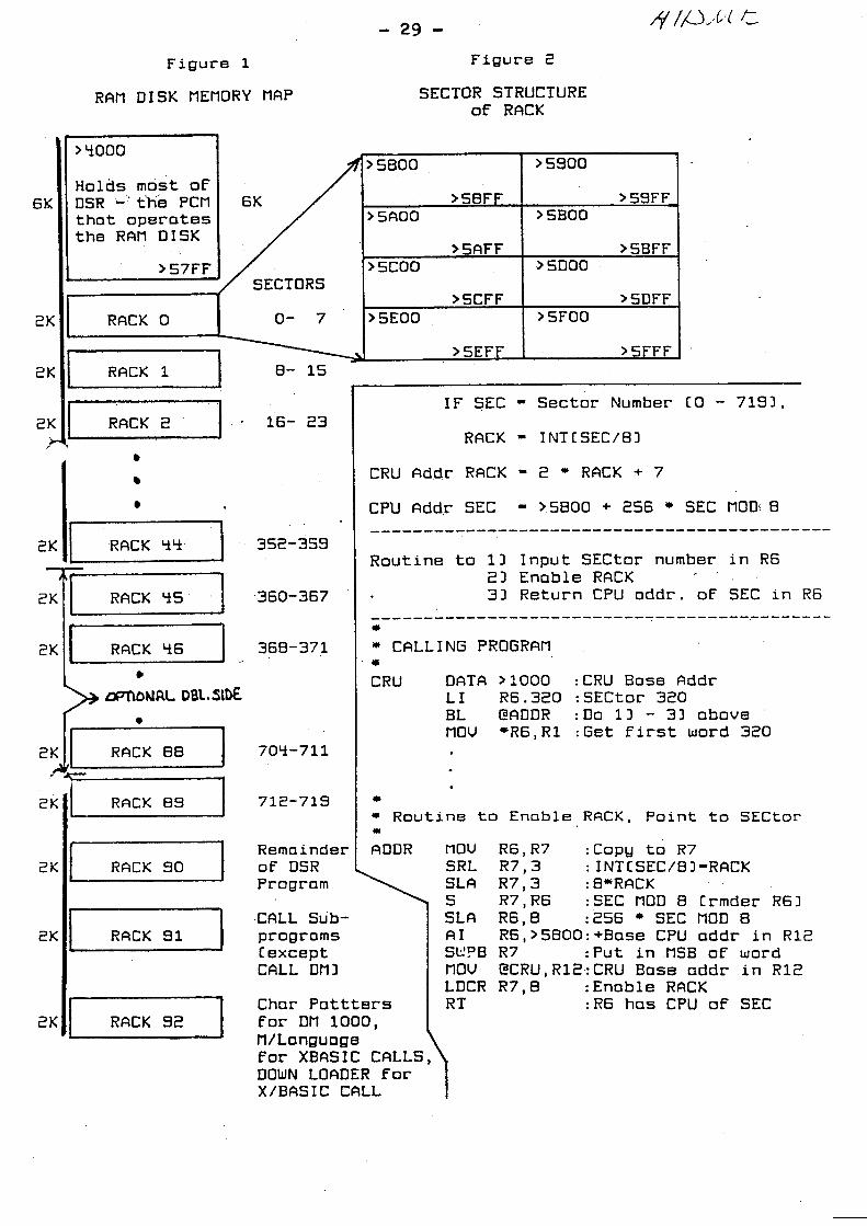
ARCHITECTURE OF THE CARD
The 4K DSR Section
Figure 1 depicts the RAMDISK memory map. A 6K segment >4000 to >57FF, is enabled every time the card is enabled. This 6K block holds most of the ROS. There is only one
memory block that can be enabled in this address space.
The 2K RACK
The remaining 2K in the DSR space is from •5800 to
>5FFF. In the >4000 to >57FF space, there is only one block of memory that can be turned on for read-write operations.

By contrast in the remaining 2K area >5800 to >5FFF, any one
of many blocks may be switched on for reading or writing data . The 2K sections that can be turned on and off in this
address space are called RAF:KS (RATS traCKS). RACKS are
numbered. The first RACK is 0 ,Dnd the last one is 92.
The RAMDISK Sector
The RAMDISK application further divides each physical RACK into logical sectors -- there are eight 25A byte sectors per RACK (See Figure 2). This division of the RACK is Purely
arbitrary in the sense that it is an artifact of our
software. A non-ramdisk application would, no doubt, use a
different logical organization for the RACKS.
Single Sided vs. Double Sided
If you have a single sided RAMDISK, you have block_l the block
in Figure 1 which have the heavy black line beside them.
This includes the first 6K, RACKS 0 through 44 and RACKS. R7
through 92. Double siding a card also adds RACKS 45 through
88;
Notice that even if you have a single sided card, you have
RAM for a few sectors of the end •of a double sided
configuration -- 712 to 719. In addition, there are three RACKS which are used as integral parts of the ROSS.
The Last Three RACKS
RACK 90.contains'portions of the•OS. Although we started out believing we could fit the program to operate the RAMDISK
in 6K, we needed nearly 8K. Portions of the code which do
not require disk sector access have been moved to RACK 90.
RACK 91 contains all of the CALL subprograms you can access
from BASIC and Extended BASIC. The only exception is CALL DM:There is plenty of room left in this block for more
CALLS or data.
RACK 92 coritairis the character patterns used by DM-1000,
starting with the cursor, ASCII 30. Following this data is
the machine language that gets downloaded for DELETE "XBCALL". Finally, RACK 92 contains the program that transfers this machine language into the low, 8K section of
the memory expansion unit. There is additional room in this
RACK for more CALLs or data.

— 20 —
HOW TO ENABLE THE 4K AREA AND A RACK
Loading the CPU Base Address •
Whenever e. CRU access is maf4e, the CRU base .address must be loaded in Workspace Register 12. If the DIP switch settings
on your card are standard, the CPU base address of the card
is >1000 -- you would place >1000 in P12, If your card is
set for CPU base address >1200, you would place that vPluP in
R12.
Calculating the RACK Code
Assuming the desired RACK number is known (0 — 92), the CPU
address of the RACK is found as shown below Figure 2 --
2 * RACK + 7. In a RAMDISK example, the stating quantity
would be the sector number (0-- 359 or 719). ThP RACK containing that sector is simply the integer value obtained
by dividing the sector number by 8.
Enabling the DSR and RACK
Once the RACK code is calculated (2 *: RACK + 7), it is placed in the most significant byte of a word, and the LDCR @WORD,8
instruction is executed. This will enable the 4K DSR section and the RACK selected.
Suppose one wanted to enable RACK 92 .(and the 4K DSR) in an
assembly language program: 0
BASE DATA >100111 ;Ba=,-e- rRu address set on DIP switch
:+: First Load CRU Base Address
START NOY PBWE,R12 ;Put base CRU actress in R12
* RACK rRU = 2 1, RACK + 7 *:
LI R1,92
;Put desired RACK in a register SLA R1,1
;Multiply by 2 - AI R1,7
;Add 7
* Put Code in Most Sig Byte of a Word
BWPB R1 ;swap most and least Sig bytes
* Enable 6K DSR and RACK 92
LDCR R1,8
* Now >4000 — >57FF is the LISP. RAM
* and >5RO1? — >5FFF is the 2K in RACK 92

Now the .e,ddrPss space >4000 to >5FFF cart be accessed as
ordinary CPI! RAM -- it car he used to load and run machine
lanpuagP, store and fetch data, et. When the DSR is
disabled, ;Ind the computer system powered down, however,
everything writtn to this area will be retained under
battery back-up.
Disabling the Card
To disable the card, load R12 with the base rRu address (usually >1000) and then simply use a SE?. 0 instruction.
* Load RI2 with CRU Rase Address
LI R12,>1000
nisA.hle the Card
SR7 0 (PR - an SRO here will turn ON
the card and RACK 0)
If you have accessed the card via a standard DSRLNK routine,
that routine will turn off the card for you upon return.
However, if you have turned it on explicitly, then you must
turn it off via your program as described above. Remember
that the card must always be turned off from a program
running in memory space outside >4000 to >5FFF -- if you try
to have the card turn itself off the computer will be faced
with a bunch of O's for machine language instructions and
quickly run amok..
LOADING YOUR OWN PROGRAMS
On your System Master diskette, you will find a few programs
that may prove useful in experiments with the DSR area.
These include a program to erase the 6K DSR and RACKS 90-92
(leaving unaffected the actual contents of the RAMDISK), and
the source and object code for a special loader which will
allow you to load object files created with Editor/Assembler
directly into the 6K and three 2K blocks.
CLEARING THE OPERATING SYSTEM
You may disable the RAMDISK operating system by executing the
UTIL1 loader program and typing an N in the column that
indicates the status of the operating system. The >AAO1 in
the DSR header is removed making the RAMDIS• invisible to
your computer. Any information actually contained in the
SECTORS of the RAMDISK will be un-,ffected by this operation
so that immediate restoration of the operating system via
UTIL1 would again allow access to all disk information.
(Natur,,tlly, if programs you write for the DSR modify sector
data, this will riot necessarily be the case!)

The LOADER
Located on your System Master disk is a source code file
called LOADER/S. When assembled and run this program loads tagged object files created with Editor/Assembler. Several •
rP,-strictions are involved, however. First, you MUST use only
Absolute Origin (AORG) code. You can use as many AORG
statements in your program as you like and can even place
code outside the >4000 to >5FFF DSR space, but LOADER will
not handle relative code.
Secondly, you must not use compressed object files. The
loader only works with uncompressed object files. Do not specify a "C" in the options prompt when assembling your
program.
Finally, on a given execution, this LOADER makes available
the standard AK (>4000 to >57FF) and one of the remaining 2K
blocks. You are asked to select which of the •K blocks you
want enabled when the loader is run. Each of the 2K blocks
(RACKS 90-92) are decoded from >5800 to >5FFF. If code is to
be placed in more than one of the three 2K blocks, this must
be done via separate executions of the LOADER program and
separately assembled object files. Code destined for a 2K
block must bP AORG'd with a value of >5800 to >5FFF (just as
code for the AK area must be AORG'd from >4000 to >57FF.)
You first write and assemble your DSR program. Save the un—compressed object file on diskette (NOT RAMDISK). Then, with the LOADER program on—line, select Option 3 (Load and
Run.) from the. E/A Main Title Screen and enter the File Name:
ErWx.LOADER
You will first be asked to enter the name of the object file
you want loadPd. First key in the disk drive number, then a
decimal point, and finally the object file name used when the
program was assembled. You can use FCTN arrow keys to .move
the cursor forward and backward. When the name is correct,
press ENTER.
Then, if the file is found, you will be asked to select which of the three 2K blocks AORG'd code from >5500 to >5FFF (if
present in your program) is to be placed. RACKS 90 to 92 are 2K blocks 1 to 7, respectively. Press key 1, 2, or 3, depending on where you want the code to go. If you have no code AORG'd over the >5800 area, it does riot mat ter which 2K
block you select.
After the file is loaded, the loader provides the highe=t
address used in both the 4K and 2K block. From this
information you can insure that you have not exceeded the
limits of the block and determine just how much space is left
in that block. If the highese address used for a block is

>0000, Ito code was loaded into that block. When using the LOADER, you need not load code into either the /1...K or 2K block
-- what gets loaded will depend upon your AORG statements.
After the code is loaded, you will be asked to press ENTER to
continue. Press ENTER, then FCTN QUIT or FCTN BACK.
EXPERIMENTING WITH DSRs
A full discussion of EVER block structure is beyond the scope of this manual. A supplementary manual is planned. However, full information can be found in TI's manual: TI-99/4A CONSOLE AND PERIPHERAL EXPANSION SYSTEM TECHNICAL DATA. Pages 54 and 55 give Assembly Language examples of EISR header formats and the accompanying text describes the techniques used to enter the DRRs as well as for returns to cAlling programs.
OnP area NOT covered in the TI manual, however, is the
writing of routinecr, which can be placed on the card and
accessed via. CALL statements from TI BASIC or TI Extended
BASIC. The remainder of this section of the manual will
describe the techniguPs involved.
THE CALL STATEMENT
Whenever the BASIC interpreter executes a CALL statement, it
searches through all potential CRU addresses to see if there
are any valir! DSR cards at those addresses. When it finds a
card, it gets the address of the CALL Table. The CALL Table
contains a list of CALL names (like SOUND, COLOR, SPRITE,. etc.) Associated with each name is the address at which that
routine starts and a pointer to the next name in that list
(if any).
After searching all cards, the computer searches GROMS to
find the name. If at any point in the search the name is found, that routine is executed and control is returned to -
the BASIC interpreter.
In order to write assembly code which will be loaded onto the
HORIZON card so as to be executed via BASIC CALL statements,
use the following following set—up program:

-24-
4-: The example program below shows the general techniques used in
• writing CALL routines. These two are CALL A and CALL BBB wh i ch,
▪ respectively, fill the screen with A's and B's when executed from • BASIC or Ext BASIC.
To try them, first run the CLEAR program. Then used LOADER to load the object file (CALLDEMO). (It doesn't matter which 2K block you select.) Once loaded you can try them out from BASIC.
General Header For DSRs
AORG •4000 BYTE >AA BYTE >01 DATA 0 DATA 0 DATA 0 DATA 0 DATA CTABLE DATA 0 DATA 0
Start of 6K area Code for valid DSR Version number = 1 not used POWER—UP LINK table address not used DSRLNK — used for OPEN, CLOSE etc CALL ROUTINE LINK table address INTERRUPT ROUTINE LINK not used
• The Link TabLe..for CALL Rout T rice
CTABLE DATA NEXT1 LINK to next entry in. table DATA FILLA ENTRY point for first routine BYTE >01 Name length 7 1 char in name BYTE 'A' Name of routine — CALL A
NEXT: DATA 0 A LINK of 0 means this is the last entry DATA FILLB ENTRY point for second routine BYTE >03 Name length — 3 bytes TEXT 'BBB' CALL BBB is name of this routine DATA 0
Use these three DATA statements for all CALLS
MASK DATA >4000 Mask for floating point error code SAVADR DATA 0 Holds return address TOKEN DATA 0
Note that both routines below start out by saving the return addres :+: and resetting the token pointer to the end of the BASIC line. :+:
:}:

• START OR FILLA
FILLA mnv R11,@SAVADR Save return address Milt/ @>832C,R1 >832C -> add• of BASIC token code pointer
this points to the byte immediately AFTER
the CALL token in the BASIC program. By advancing this value you may read data
directly from the remainder of the program statement. Ultimately, it must point to the End-of-Line mark 1 01" in the BASIC program an in this case the rame only contains 1 char.
INC R1 MFIV R1,@TOKEN Save in TOKEN for return
* Now do the routine - fill the screen with As
LI R1, .:A100 CLR RO SOC (MASK, F:0 SWPB RO MOVB RO, @>8CO2 SWPB RO MOVB RO, @>8C0': LI R0,748
ALOOP MOVB R1,P>8C00 DEC RO JNE ALOOF' B (RETURN
*
"A" /-5,+94 offset for basic
Starting VDP RAM address indicate a write LSB First Move into VDPWA Now MSB to VDPWA 748 "A"s to write Write a byte to VDF'WD (auto incrementing) Done?
Done, use common return routine ■
* START OF FILLB
FILLB MOV R11,@SAVADR Save return address MOV P,>832C,R1 Get token pointer AI R1,3 This name is 3 chars so must add 3 to
get to-the end 0; the BASIC line MOY R1,@TOKEN Save token pointer
* Now do routine ("*".4, 4.:
LI R1, >A200 CLR RO SOC 1.MASK,R0 SWPB RO MOVB R0,0>8C0:7' SWPB RO MOVB R0,@>8CO2 LI R0,768
BLOOP MOVB R1,@>8C00 DEC RO JNE BLOOF' B @RETURN
*:
"B" 44+94 offset for basic Starting VDP RAM address indicate a write LSB First Move into VDPWA Now MSB to VDPWA 768 "B"s to write Write a byte to VDPWD (auto incrementing) Done?
Done, use common return routine

:+: You can use the following code in any program. If you :+: need to return with an error. B n ERTN. Otherwise,
* B (i4RETURN.
:+: Error Return — use for INCORRECT STATEMENT error :+:
ERTN LI RO,>0700 MOVB RO,@>8342
Make •07 the current token/char JMP RTN
* Non—error Return
RETURN SZCB e>8342,@>8342 Make •00 (End of Line) the current token
RTN MOV tSAVADR,R11 Restore Return Address MOV eTOKEN,R1 Get Token Pointer
'_:WPB R1 LSB First MOVB R1,12>SCO2 Move to vnP Write Address _WPB R1 MOVB R1,@>81:02 Now do MSB MOV R1,(2>832C • This resets token pointer INCT R11 SZCB @MASK,@•8354 Floating point error
B *R11 END

- -27 -
MEMORY MAP OF HORIZON RAMDISK OPERATING SYSTEM
VERSION 04
>4000 - >57C7 Main DSR
1st 2K Block: RACK 90 - LINK1 = BBOO
>5800 - >5EDB Portions of DSR code that db riot require access to RAMDISK contents. These are accessed via PTCHxy labels and return via RTNX labels.
2nd 2K Pluck: RACK 91 - LINK 2 = >BDOO
>5800 - >5801 CALL Subprograms except CALL DM which is in PARTD.
3rd 2K Block: RACK 92 - LINK? = >BFOO
>5800 - >5BOF Pattern definitions for 98 characters used by DM-1000.
•5810 - >5E19 Machine language for the Extended BASIC analogs of the CALL subprograms.
•5E1A - )5E61 Definition table showing the names of all the XB CALL analogs.
>5E62 - >5ED1 DELETE "XBCALL" code used to download the XB call analogs.

- DISK CONTENTS -
PARTA-E - Source code for five parts of the main DSR.
Use the COPY directive in E/A to assemble into
ore object file.
CALL/S - Source for CALL subprograms (except CALL DM).
CHAR/S - Pattern definitions used by CALL DM.
XB/S - Extended BASIC analogs of CALL subprograms - low 8K.
DOWN1 D/S - DELETE "XBCALL" rout i ne
SVXB/S - Uploads the XB/O code to its place in the third 2K block. Program name is SVXB. Executed as follows: >CALL INIT
>CALL LOAD("DSK1.XB/0")
>CALL LOAD("DSK1.SVXB/0")
>CALL LINK("SVXB")
CREATE/S - Creates PARTA_xy and PARTB_xy memory image files holding whatever is in the 12K of DSR space. (:::'4000->5FFF plus the three 2K blocks).
LOADER/S - Source code for loader for uncompressed tagged object code AORG files.
PARTA_04 PARTB_04 - Memory image files of DSR. Used by UTIL1.
MGR1
MGR? - Memory image files for DM-1000 Ver. 7i.3.
LOAD - Extended BASIC auto-load program for UTILl,
DM-1000 and MEMTEST. Requires YLOAD file.
UTIL1 - Loader for Ramdisk Operating System.
MEMTEST - Test program for Horizon Ramdisk. TEST/0 file.
DOCUMENT Details DSR subroutines as to Work Space,
Register symbolic addresses, etc.
TiMnOCPT1
DMDOCPT4 - Documentation for DM-1000.
2K F RACK 2 1 16- 23
2K RACK 44
• •
•
352-359
-360-367
368-371
* Routine to Enable RACK, Point to SECtor *
Remainder ADDR MOU R6,R7 :Copy to R7 of DSR SRL R7,3 :INTCSEC/83-RACK Program SLA R7,3 :0*RACK
R7,R6 :SEC MOD 8 Crmder R6) CALL Sub- SLA R6,8 :256 * SEC MOD 8 programs AI R6,>5800:+Base CPU addr in R12 (except S1!PB R7 :Put in MSB of word CALL DM) MOV @CRU,R12:CRU Base addr in R12
LDCR R7,8 :Enable RACK RT :R6 has CPU of SEC Char Pattters
for DM 1000, M/Language for XBASIC CALLS\ DOWN LOADER for X/BASIC CALL
704-711
712-719
8- 15
>5600
>SOFF
>5900
>59FF >5A00
>SAFF
>5800
>58FF, >5C00
>SCFF
>5000
>SDFF >5E00
>SEFF
>5F00
>5FFF
6K
RACK 1
2K
2K
RACK 45
RACK 46
•
DRTIONIAL DBL.SIDE
•
RACK 88
RACK 89
RACK 90
RACK 92
SECTORS
0- 7
2K
2K
6K
2K
2K
IF SEC - Sector Number CO - 719),
RACK - INTCSEC/8]
CRU Addr RACK - 2 * RACK + 7
CPU Addr SEC - >5800 + 256 * SEC MOD 8
Routine to 1] Input SECtor number in R6 2) Enable RACK 3) Return CPU addr. of SEC in R6
* * CALLING PROGRAM 46 CRU DATA >1000 :CRU Base Addr
LI R6.320 :SECtor 320 BL @AMR :Do 13 - 3) above NOV *R6,R1 :Get first word 320
*
'>4000
Holds most of DSR •-' the PCM that operates the RAM DISK
>57FF
RACK 91 4
- 29 - 7/ //..),,G(
Figure 1 Figure 2
RAM DISK MEMORY MAP
SECTOR STRUCTURE of RACK
HORIZON RAMDISK
CONSTRUCTION GUIDE
by
p."-■ Ron Grim'
COPYRIGHT 1585, Horizon Computer, Limited
ALL RIGHTS RESERVED
-31 -
••••••••••••••••••••••••••••••••••••••••••••••••••••••••••• • • O THE CONSUMER ASSUMES FULL RISK AND LIABILITY FOR DIRECT * • OR CONSEQUENTIAL DAMAGES ARRISING FROM ATTEMPTED CON- 0 * STRUCTION OF THE HORIZON RAMDISK. • • O EXCLUSION OF WARRANTIES: The HORIZON RAMDISK circuit • board is provided on an AS IS basis. No warranty of • • any kind is assumed by Horizon Computer, Limited. The * • user assumes full responsibility for quality of all • * parts associated with construction of the HORIZON RAM- * O DISK. Horizon Computer, Limited does not recommend or * * endorse the quality of parts sold by any third party. 0 * In any case, Horizon Computer, Limited shall be liable 0 • only for the cost of the circuit board, associated man- * * uals, and disk based software. 0 • • a Fully constructed HORIZON RAMDISKS are available with a 0 O 90 day limited warranty for an additional cost covering 0 * parts and labor. Contact Horizon Computer, Limited for * O current price and availability. • • •••••••••••••••••••••••••••••••••••••••••••••••••••••••••••
Prior familiarity with construction of digital circuits is assumed. Read all construction suggestions and notes provided with the eight figures before proceeding. The following eight pages show progressive stages in completion of the HORIZON RAMDISK. If you encounter a problem or have a question at any step DO NOT PROCEED UNTIL THE PROBLEM IS RESOLVED. If you have any questions contact: Ron Gries (419) 874-9638, or David Romer (419) 666-6911.
Although static can be a problem with CMOS devices (i.e. the 5264LS-15's) we have not seen a single case of IC damage under ordinary handling procedures; nor have we seen problems do to excessive heat. While you may decide to take precautions against excessive static and heat
P-N transfer, remember thatt.it is equally important THAT ALL SOLDER CONNECTIONS ARE OF GOOD INTEGRITY.
Use a low wattage (about 25 watts) soldering pencil and fine 60:40 tin/lead solder. DO NOT USE a soldering gun or acid core solder! Make sure that sufficient solder is supplied to all connections with good wet-out, but that there are no solder bridges between connections. Upon completion of all soldering, remove flux from the solder side of the board with a commercial flux remover.
When inserting IC's bend the pins to fit the socket by placing the IC on it's side on a flat surface. Bend the pins against the surface by moving die body of the'IC. Make sure all pins are properly aligned with the socket holes and that all pins actually go into the socket holes upon insertion.

•
• • • •
■ • •
•
Ilse • • • irv—i • • • • • •
• • •
• • •
• • • •
• • • •
•• • • •
• • • • • •
•• • • •
•
• • • • •
• •
• • • •
•
• • Tp
• •
• •
• • • • •
• •
•
• •
•
•
• •
• •
•
• 0* • 0 • Se •
• ego •
foe • •• •
- 32 -
NOTCH
• • • • • • • • --w—T "---w—i T-1,--T ----w—T
i
1
• o • •
• • •
• • • • 4 • • •
• a • 0
• • • • ,••••■••••,,,,■11V • •
111111111111111111111111111111
FIGURE 1
The sockets required are: 13 28-pin, 1 2'i-pin, 3 20-pin, S 16-pin and 1 lq-pin.
Referring to Figure 1, place all sockets on the board. The sockets are inserted on the side of the board on which all parts are labeled. The sockets you use may be notched on one end. If so, orient the notches as shown. If your sockets are not notched, orient them with the pin 1 mark in the upper left corner. Note that sockets are not used for the JACK and SWITCH positions.
Place a piece of cardboard or other stiff material over the sockets to hold them in place, and turn the board upside down for soldering. When soldering the corner pins of each socket, apply a little pressure to the board to insure that the socket is all the way in. Do not apply excessive amounts of solder
Upon completion of soldering, carefully inspect your work to insure that there are no solder bridges between pads.
A 16 pin socket may optionally be Lised for the DIP switch, labeled "switch" on the PC board.
0CD0 or-Js •CD• 0CD• ■ • • •
• • O •
•
S I
44 • •
• •
• • •
- 33 -
• 4
•C:1•• •C:!•
•
!J lit II(D. Tan tal
s
•
11 JI111111 J1111111U1111111111
• • •
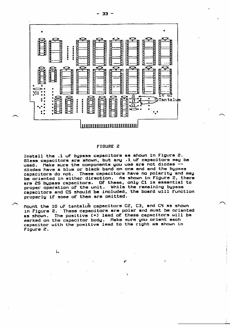
FIGURE 2
Install the .1 uF bypass capacitors as shown in Figure 2. Glass capacitors are shown, but any .1. uF capacitors may be used. Make sure the components you use are not diodes --diodes have a blue or black band on one end and the bypass capacitors do not. These capacitors have no polarity and may be oriented in either direction. As shown in Figure 2, there are 25 bypass capacitors. Of these, only Cl is essential to proper operation of the unit. While the remaining bypass capacitors and CS should be included, the board will function properly if some of them are omitted.
Mount the 10 uF tantalLA capacitors C2, C3, and C4 as shown in Figure 2. 'These capacitors are polar and must be oriented as shown. The positive C+) lead of these capacitors will be marked on the capacitor body. Make sure you orient each capacitor with the positive lead to the right as shown in Figure 2.

FIGURE 3
Refer to Figure 3 for diode placement. Three diode types are shown: CR3, CRS, and CR10 are 1N914 silicon diodes; CR4, CRS, CRS, and CR7 are 1N34A germanium diodes; and CR8 is a 1N4001 rectifier diode. Although similar in appearance, the 1N914 silicon diodes are smaller than the 1N34A germanium diodes.
Diodes are polar. In the ->1 notation the arrow points toward the cathode (-). Silicon and germanium diodes have a black or blue band on .one end to indicate the cathode (-) lead. The rectifier diode will likely be black with a silver cathode band. Make sure the components you are working with are banded (glass bypass capacitors look similar but are not banded), and make sure you orient each diode with the cathode band in the direction shown in Figure 3.
Next install the 2 Light Emitting Diodes (LED's). LED's have polarity, and the cathode (-) of those you are using will be indicated by a Flat side on the LED body or the shorter of the two leilds. Orient the LED's as shown in the inset. CR2 should be installed so that the lens points toward the front of the card but does not extend bey9nd the card edge.
• • • • • • • • •
•
3'I
•
1N914
•CD• •CD• T-11"—Ir ir"•—"T
• • • • • • • • • • 0
• •
• •
•CD•
•
40, <=:), ∎ a • • • •
• • •
•CD• •D•
GI 01N4001
1N91.4 *C.> qmpur .45prr st=>.
1; AN tr.
•i=o• CD,
1N34A 111111111111111111111111111111
•C• •CD• •C:vo •C)*
•• OO
OO
OO
•• O
OO
OO
O
1.1.1.1■1•0.1
•

•C:,• sC=)* •Cn• •0• •CD• Tr"
•• • •• • • • • • ■ •• • •
•
J •C=D• *CD* IsCps •O• *Cos
270.n •CrOm./15.
270011 441:0• *MD. /-1.:Volli>"fraC=" °C).
"-C3-•
■2N2222
e•—
ti
4=0 Kips/ 5.;.). •CD• ..00■• 0 1' •-CP-•
•1/414...• 0-00-• .4 •MMYst
• •
27 0 0 -t1
•
4=-:p• o.
Hi I
■•■••■■■,•■■•
SWITCH
- 35 -
•
•
1111111.11111111111111111111111
FIGURE 4
Mount resistors R2 - RS and R10 as shown. Although resistors have no polarity, you may'orientAham So that the color codes canbe read from left to right. 'Resistor values and corresponding color 'codes aes'asfollowti' -
R2 270 Red Violet BroWn RS 2.7K Red Violet Red
R3 2:7K Red Violet'Re• R7 2.7K Red Violet Red
R4 2.7K Red Violet Red
RB 2.7K Red'Violet'Red
RS 10K Black Brown Orange
R10 2.7K Red Violet Red
Install the 2N2222 transistor 01. From the top starting with the tab and going counter clockwise the three pins of 01 are emitter, base, and collector CE B and C). Solder the leads so that the case stands about 1/4" above the surface of the board.
Install the El-position DIP switch as shown. Solder the leads with all switches in the OPEN or OFF position. Then place switch 1 in the ON or CLOSED position as.shown.

i■•••■•••■•••••■r
•K=•• {D• •C=3•
270.rx •CD• •CD•
33-a ICD• 41:73. 6C::71
TEMPORARY JUMPER
- 36-
BATTERYS
04INCI-* or-.?+.(AID4 sajp... *crap. «nr›.• 'Mae
•CD• •CD•
•0=11• •CD■-•
sc.:), ea <De e't=" •
•C::• d=i• 4=3*
- 37 -
• •
: •• • • • •
. •• • •
V.
AM.* oc=3.01104 AUM3*W2C4 ow:340MM*
..._03,,,imp.,AMD AM*
*-C70-0* 1.-‘44=0" L./0CM
CI:.4=354' 04=114
1 sL 1
*=710 *CD* • *CDs
111111111111111111111111111111,
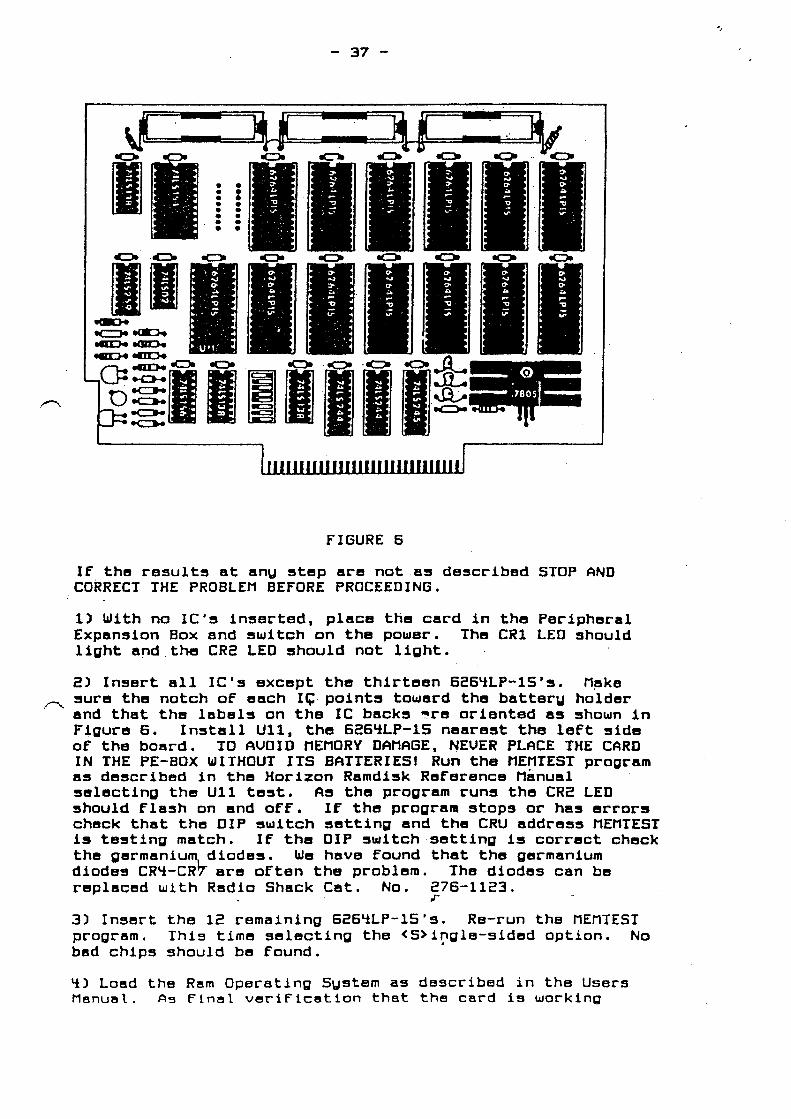
FIGURE 6
If the results at any step are not as described STOP AND CORRECT THE PROBLEM BEFORE PROCEEDING.
1) With no IC's inserted, place the card in the Peripheral Expansion Box and switch on the power. The CR1 LED should light and the CR2 LED should not light. •
2) Insert all IC's except the thirteen 6264LP-1S's. Make
f"'": sure the notch of each lc points toward the battery holder and that the labels on the IC backs mre oriented as shown in Figure 6. Install Ull, the 6264LP-1S nearest the left side of the board. TO AVOID MEMORY DAMAGE, NEVER PLACE THE CARD IN THE PE-BOX WITHOUT ITS BATTERIES! Run the MEMTEST program as described in the Horizon Ramdisk Reference Manual selecting the Ull test. As the program runs the CR2 LED should flash on and off. If the program stops or has errors check that the DIP switch setting and the CRU address MEMTEST is testing match. If the DIP switch setting is correct check the germanium diodes. We have found that the germanium diodes CR4-CR7 are often the problem. The diodes can be replaced with Radio Shack Cat. No. 276-1123. I-
3) Insert the 12 remaining 6264LP-1S's. Re-run the MEMTEST program. This time selecting the <S>ingle-sided option. No bad chips should be found.
4) Load the Ram Operating System as described in the Users Manual. As Final verification that the card is working

- 38
FIGURE 7
Eleven 6264LP-15's may be added to increase Ramdisk capacity to 720 sectors. Before soldering, test the new IC's by replacing U3-U8 and U12-U16. Use the MEMTEST program or the Disk Manager 2 comprehensive test. Remove the IC's and arrange into eleven pairs.
For one IC in each pair, cut the narrow . and of pin 20. Looking at an IC from the top with notch up, pin 20 is the sixth from the bottom On. the right side.' Bend the remaining pins inward so they make firm contact when.placed over the bottom IC. Making sure notches are matched, place top IC (pin 20 cut) over the bottom IC. •
r
Keep the ends of the bottom IC pins free of solder and scrape off flux before reinsertion. THE INTEGRITY OF EACH SOLDER JOINT IS VERY IMPORTANT. After soldering and carefully inspecting an IC pair, re-heat each joint to INSURE GOOD WET-OUT OF BOTH PINS.
Bend the remaining portion of cut pin 20 out slightly and solder one end of a 10" piece of wire-wrap wire (e.g., 30-24 AWG) to it. Insert each pair in a socket. Cut the wire to the correct length and connect to the appropriate JACK hole!r. Finally, arrange the wires between the IC rows as shown.
IC -->JACK IC -->JACK IC -->JACK U3 --> 1 U6 --> 4 U12.--> 7 U4 --> 2 U7 --> S U13.--> 13 U5 --> 3 U8 --> 6 U14 --> 14
IC -->JACK U15 --> 15 U16 --> 16

• a 4.11 ■-• a a A - v 4.0113. ;
O .1 6.1
N4
0 F.
.1
♦ 44. a .4 01 41
0+0000 00p
gip
4) ■•• •
• • •
> a ♦ 0 •V ON alb
a
2.1 .4 0 0i•I. •
>Ala
c C
■111111111111111111111111111111111111111•11111111111111111111111111111■
• C
0 • C
ON 4.
04.s .1
1.4
14. ♦
-.1 O
0 • •
•
■1111111111111111111111111111 111111111111111111•111111111111■
a 21 0, '4 C NIL;)
a • C +0• ♦ ••• A 0 A 4.
O
ON
ON
a- xna. • a-c +0 +0-,
4.0 C TO '00 "4 •-• A '
.4 X nat. C TO a0
010
0...)
A X n • a C +.0 10
a C1 T. a.0 +0 '90
I 111111- 1j 1[11111111111111 11
o.o 11111111 11111 -111- 1- 11- 11 -1C11 III
0 • •
41111
sa
C:
AAA as aA A u* AA AO> •• "
- .. • • • . • . ..
.. a •
0.
•
FFr- •
• 10 040
♦ .74 • Li a
114.30+ "c
C 32.
V C •
70
C
1:411.41-. n 01,11
O •• .0 14 •
0••••• C
■11111111111111111111111111111111111111111111111111111111111111111111■111■
111111111111111111111111111111111111111111111111111111111111111111111.1111111
■111111111111111■11111111111111111111111111111M11111M1111111111■
111111111111111101111111111111111111111111111111111111101
•
111111111 11
■■1111111111•1111■11111111111111111111111111111111111111111111111
■IIIMIIIIIIIIIIIIIIIMMI1111111111111111111111111111111■
I I I j J I 1
0
O
VI 0 0 0 0 NJ ..., 8-. * r.4 Cp '4 ,C. g.4 „t, ... .., ..
-).4 .1 CCCC CC=CC-4C 00 n .0 n re, a= ro X 02X :0 1 t1 ..I .- n • n
a z :v x .... a ,0 t„, u■ .... • ..., col ,• or 0 .., .. ...
= .0.0.07/ ..4.-.00
0 ., C II. 4- cn C
P.. V . 4
X • IN. •
A 11112 a 4.■ •-• n 4..0 ....
:.+ -. p..) ner_ ,..., 7: a X .4 r C 0 4. n r. n -.1-2.2- W.
J. 0 -4 :.1 . C •
? CI 1. .N Lii, .1 U.
A . • .4 C . C C
1:7 - -4 •i ..,
i -4 0 0 IV 11
... •-• .
.RCN ..4 0
cr . ..,
.0 X rl #4 I
:v 00 x 7, ,1 Ir. Ord Cl.... c
1 3 40 ..0
so a. 1. V)
1$4. • ri . C .... ... .4 •-• P...• C
0 ..1
0■1 • 0 10 A a 0 ....
X 0 . 0 r. 0 ....t .-•
.t.. 0 • .x. N. Qv a rs 1 P4 a Q f• --I X Z 4. • 014* X r 9
4, r r'
(..0 t7, LA -i ^4 0 0•.• a ...1 ...1
P., • 0 0 ...j 1. 1. 1. .1.. ....1 . C . j. J. a., = • It 'X
*4 .1 .-. 0 0. 0 .... .. r•
• a `... a •
'‘... •-• rt: -.1 (4 4...
a. to LA .<
CD 0. -1 w -i 0 r- r- t- t- ch c: -- t; r• r-
4. 0 .1 1.1 :0 tn LA u) LA ♦ .• w, •4 VI N 0 IV 44 n .. a . •:. v 4 a 0 u..)
z • C r to
•A t', .0
< If T
r- v • - a p.4.0r.j... .4... In .4 . lc . . 1.0 V 1•-• - 4 ..) as LA 14 -0 LA LA T 7 23 (A
0 C) C) 0 &A • I:. .• V, 21 t .. •-• .• •-• ...
r. ri x u. 13 -13 z 'A 0
1./ . ..0 Pg
0 O. " ? F. ? °
0 0 •-• to r
1 A . a A
.4 le Zs ...
PIP C 0 1.-...p., ...... L., ..... L., .. ... 4,, .......c- I. .1 J. P.I LP
a : 2 a
w0
0 C
OP
YR
IGH
T P
M RO
NA
LD G
M)
4.1 .7. •
a 0 4.
• -
• to. a+ .0 N 0 • .4
r. t 4: ..... a ZI=Ci5: 4 ;41 0
..... 0 LA
0 0000000 10 0 "" 04 14 A V. 0 .4 z
••• 14 IC/
• s • r. cso 7,c
'`ifattiZtg
• • • ‘0, N " 0 ).
1_111111 J1111111F1111111 I I
11111111 IIIIIIIIIJHJ111 11
C
11111111111111111111111111111111111111,1111111111111111111111111111
111111111111111111111111111111111111111111111111111111111111111111•11111
ummuummommummuummom
■111111111111111111111111111111111111111111111111111■1111111■
1111111.1 1111111111J1 -1111 If C •■•0 VO•. n
t
Top Related