


![Stirlingengine - ifisc.uib-csic.es engine.pdf · Stirlingengine ... The Stirling engine (or Stirling’s air engine as it was ... design[12]inwhichapplicationitisnowgenerallyknown](https://static.fdocuments.us/doc/165x107/5ab50eff7f8b9ab47e8c825d/stirlingengine-ifiscuib-csices-the-stirling-engine-or-stirlings-air.jpg)

Languages
Pages
Legal

Guided-Wave Optical Wavelength-Manipulating Devices Using Electrooptic Effect
Hiroshi MURATA and Yasuyuki OKAMURA
Osaka University, Graduate School Engineering Science, Department of Systems Innovation,
Area of Advanced Electronics and Optical Science
1-3 Machikaneyama, Toyonaka, Osaka 560-8531 Japan
Guided-wave devices with the first-order electrooptic effect (Pockels effect) and polarization-reversed structures have been
studied and developed for applications to optical wavelength/frequency manipulation. The electrooptic effect has potentials for
precise and continuous optical frequency manipulations with a tuning frequency range of ~100GHz and an operation wavelength
bandwidth of over 100nm. The authors have proposed and developed several novel electrooptic guided-wave devices, low-power
and low-chirping optical intensity modulators, optical single-sideband modulators operated with one driving RF signal, and optical
frequency shifters, using the polarization-reversal technology of ferroelectric materials. In this paper, the basic structures, the op-
eration principles, the analyses, the fabrications, and the experimental demonstrations of the proposed devices are reported. The
application of the developed electrooptic single-sideband modulators to radio-on-fiber systems for the transmission of microwave
mobile signals is also presented.
KEYWORD: electrooptic modulator, optical waveguide, LiTaO3, LiNbO3, polarization-reversal, optical integrated circuits, SSB
modulator, optical frequency shifter, radio-on-fiber system
1. Introduction
The first-order electrooptic (EO) effect (Pockels effect)
in ferroelectric optical materials, such as LiNbO3 and Li-
TaO3, has an extremely fast response time of less than pi-
cosecond order and an ultra-wide wavelength bandwidth of
over several hundred nanometers1,2). These characteristics
are very attractive in device applications for optical wave-
length/frequency manipulations in many optoelectronics
systems. With the use of the EO effect, precise and con-
tinuous control of optical frequency in a tuning frequency
range of ~100GHz and an operation wavelength bandwidth
of over 100nm is expected.
Recently, studies about the polarization reversal (domain
inversion) of ferroelectric optical materials and its applica-
tions to nonlinear optical devices have attracted consider-
able interest, and many excellent optical wavelength-
conversion devices have been reported 3-9).
Another interesting application of the polarization-
reversal technology is the EO device. The polarization-
reversed structure is applicable to several EO optical
modulators based on ferroelectric materials (LiNbO3, Li-
TaO3, KNbO3, etc.), and it enables us to construct novel
devices with advanced functions and perfomances10-12).
These devices are also attractive for applications to optical
wavelength/frequency manipulations[P1, P3].
We have proposed and developed several types of novel
EO guided-wave devices utilizing the polarization-reversal
technology. In this research project, we further studied the
proposed devices in terms of their applications to wave-
length/frequency manipulations and demonstrated their
performance. In this paper, the basic structures, the opera-
tion principles, the analyses, the fabrications, and the ex-
perimental demonstrations of the proposed devices are
reported. The application of the developed EO single-
sideband (SSB) modulators to the radio-on-fiber systems
for the transmission of quasi-millimeter-wave mobile sig-
nals using long silica optical fibers [P17] is also presented.
2. Background
2.1 Guided-wave EO modulators
EO guided-wave devices are very important in optoelec-
tronics systems, and a tremendous number of studies about
the EO functional devices have been published over the
last 30 years. Today, LiNbO3 guided-wave modulators are
widely used for long-haul optical fiber communication
systems and optical signal processing systems2, 13). Re-
cently, high-speed and low-voltage LiNbO3 traveling-wave
electrode intensity modulators operated at 40Gbps with a
half-wave voltage of ~1V have been reported14).
The EO effects cause an electrically induced index
change in optical materials, therefore, a basic EO modula-
tor is a phase modulator. By combining the EO effects
with several guided-wave elements, such as a Mach-
Zehnder interferometer, junctions, and directional cou-
plers, the electrically induced optical index change is con-
verted to other optical phenomena (interference, mode
conversion, coupling, etc.), and many useful EO devices
for optical intensity modulators/optical switches, mode
converters, and deflectors can be constructed.
By applying the polarization-reversal structure to these
EO guided-wave modulators, the following interesting
effects can be obtained.
a. Quasi-velocity-matching in traveling-wave modulation
b. Control of modulation polarity
c. Control of modulation depth and phase
Utilizing these attractive features, the following novel de-
vices with advanced functions and performances have been
realized.
1. Quasi-velocity-matched (QVM) EO phase modulator
2. Low-power and low-chirping EO intensity modulator
3. EO optical SSB modulator/optical frequency shifter
We previously proposed and developed the QVM EO
phase modulators10, 11). In this research project, we pro-
posed and developed low-power EO intensity modula-
tors[P13], EO SSB modulators[P3, P5, P8, P16, P17] and optical
frequency shifters[P18]. In the next subsection, a review of
QVM EO phase modulators is presented.
Photonics Based on Wavelength Integration and ManipulationIPAP Books 2 (2005) pp. 213–224
213
2.2 QVM EO phase modulator
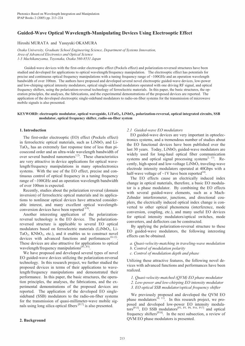
The basic structure of the QVM EO phase modulator is
shown in Fig. 2-1. It consists of a single-mode waveguide
and traveling-wave coplanar electrodes formed on a ferro-
electric material substrate with a periodic polarization re-
versal. The length, L, of the polarization-reversed and
non-reversed region for the QVM is determined by the
following equation.
(2-1)
where fm is the designed modulation frequency, vg is the
group velocity of light propagating in the waveguide, and
vm is the phase velocity of a modulation wave traveling
along the electrodes. It should be noted that not the phase
velocity of the lightwave, but its group velocity must be
considered, because EO modulation is a three-wave mixing
process and the interaction among the lightwave, modula-
tion wave and modulated lightwave (sideband) should be
compensated by the periodic reversal.
Applying the periodically polarization-reversed structure
to the traveling-wave modulators, velocity mismatching is
compensated similarly to that in QPM SHG devices.
Therefore, accumulative modulation over a long interac-
tion length is obtained at the designed frequency without
using specific electrodes or waveguides for velocity match-
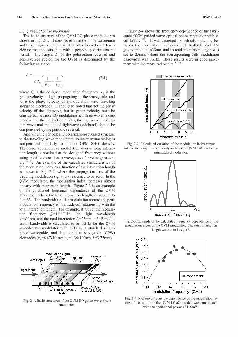
ing15, 16). An example of the calculated characteristics of
the modulation index as a function of the interaction length
is shown in Fig. 2-2, where the propagation loss of the
traveling modulation signal was assumed to be zero. In the
QVM modulator, the modulation index increases almost
linearly with interaction length. Figure 2-3 is an example
of the calculated frequency dependence of the QVM
modulator, where the total interaction length, Lt was set to
Lt = 6L. The bandwidth of the modulation around the peak
modulation frequency is in a trade-off relationship with the
total interaction length. For example, if we set the modula-
tion frequency fm=16.4GHz, the light wavelength
=633nm, and the total interaction Lt=25mm, a 3dB modu-
lation bandwidth is calculated to be 6GHz for the QVM
guided-wave modulator with LiTaO3, a standard single-
mode waveguide, and thin coplanar waveguide (CPW)
electrodes (vm=6.47 107m/s, vg=1.36 108m/s, L=3.75mm).
Fig. 2-1. Basic structures of the QVM EO guide-wave phase
modulator.
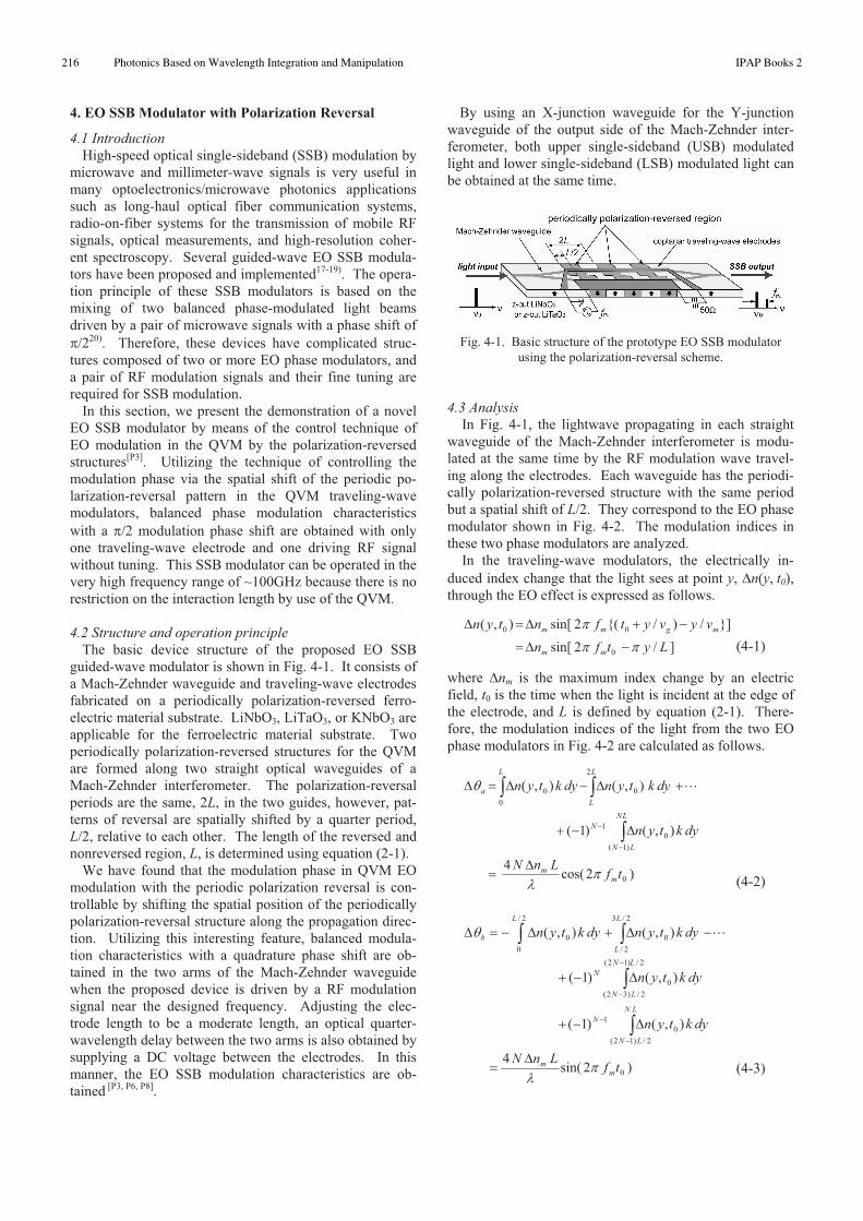
Figure 2-4 shows the frequency dependence of the fabri-
cated QVM guided-wave optical phase modulator with z-
cut LiTaO310). It was designed for velocity matching be-
tween the modulation microwave of 16.4GHz and TM
guided mode of 633nm, and its total interaction length was
set to 25mm, where the corresponding 3dB modulation
bandwidth was 6GHz. These results were in good agree-
ment with the measured results10, 11).
Fig. 2-2. Calculated variation of the modulation index versus
interaction length for a velocity-matched, a QVM and a velocity-
mismatched modulator.
Fig. 2-3. Example of the calculated frequency dependence of the
modulation index of the QVM modulator. The total interaction
length was set to be Lt=6L.
Fig. 2-4. Measured frequency dependence of the modulation in-
dex of the light from the QVM LiTaO3 guided-wave modulator
with the operational power of 100mW.
gm
mvv
f
L11
2
1
214 Photonics Based on Wavelength Integration and Manipulation IPAP Books 2

3. Low-Power and Low-Chirping Intensity Modulator
3.1 Introduction
EO Mach-Zehnder waveguide intensity modulators are
very important and widely used in long-haul optical fiber
communication systems, radio-on-fiber systems, optical
measurements, and so on. In this section, novel EO Mach-
Zehnder intensity modulators with the polarization-
reversed structure[P13] are presented. Utilizing the polariza-
tion-reversal technology of ferroelectric materials in the
Mach-Zehnder intensity modulators, it is possible to
achieve low-power and low-voltage modulation character-
istics. In addition, push-pull modulation characteristics
with a complete balanced modulation depth are obtained
by using only one traveling electrode without the need for
precisely tuning. This leads to extremely low (~zero)-
chirping modulation characteristics. The basic structure of
the proposed device, the design, and the experimental
demonstrations are presented.
3.2 Device structure
Basic structures of the proposed EO intensity modulators
are shown in Fig. 3-1. The spontaneous polarization in one
straight waveguide of a Mach-Zehnder interferometer is
reversed by the polarization-reversal technique, while it is
not reversed in the other straight waveguide. In Fig. 3-1
(a), the two ground lines of symmetric coplanar electrodes
are set on the two straight waveguides of the Mach-
Zehnder interferometer, respectively, while in Fig. 3-1 (b),
two edges of the hot line are set on the two guides, respec-
tively. In these configurations, the direction of modulation
electric fields in the two guides are the same, however, the
signs of the index change in the two guides are opposite
because of the polarization reversal. Therefore, push-pull
modulation characteristics are obtained. The separation of
the hot and ground electrodes, which determines the
strength of modulation electric fields for a given voltage,
can be shortened compared to conventional single-
electrode Mach-Zehnder modulators, whereby the driving
voltage is lowered. In addition, chirping caused by the
slight difference in the EO index changes between the two
guides is negligible since the distributions of the modula-
tion electric field across the two waveguides are symmet-
ric. It is also possible to adopt this structure in periodi-
cally polarization-reversed schemes and to construct QVM
intensity modulators with band modulation characteristics[P13].
3.3 Experiments
The polarization-reversed intensity modulator in Fig. 3-
1(a) was fabricated using z-cut LiTaO3. Figure 3-2 shows
a typical example of the experimental results of the inten-
sity modulation in the fabricated polarization-reversed
modulator with the structure shown in Fig. 3-1(a). In the
experiments, the light source was a He-Ne laser of 633nm.
The measured half-wave voltage, V , was 2.4V, which was
in good agreement with the calculated value of 2.3V for
the proposed device with the 20mm-long electrodes, while
it was 4.4V in the Mach-Zehnder intensity modulator with
the conventional single electrodes of the same electrode
length. Using optimized device parameters and a long
(~30mm) electrode, the half-wave voltage is calculated to
be below 1V. A device with the structure shown in Fig. 3-
1(b) was also fabricated and its operation with a lower
driving voltage was also verified.
Fig. 3-1. Basic structures of the proposed EO guide-wave push-
pull intensity modulators with polarization reversal.
Fig. 3-2. Example of the modulated output from the fabricated
polarization-reversed intensity modulator.
3.4 Summary
Novel polarization-reversed Mach-Zehnder intensity
modulators are proposed and their operations are pre-
sented. We are now in the progress of designing and fab-
ricating low-power intensity modulators operated in the
IR-wavelength region used in optical fiber communica-
tions, and of measuring their chirping characteristics.
The proposed polarization-reversal scheme can be com-
bined with several velocity-matching techniques. For ex-
ample, combined with the etched ridge waveguide struc-
ture and the thick electrodes15), base-band, low-power and
low-chirping modulators are obtained. When this structure
is combined with the QVM technique described in section
2.2, band-operated, low-power and low-chirping modula-
tors are obtained[P13]. It is also possible to apply this struc-
ture to the EO SSB modulators with the periodically po-
larization-reversed structures with quarter-spatial shifts[P12].
These high-performance SSB modulators are presented in
detail in section 5.
215Photonics Based on Wavelength Integration and Manipulation IPAP Books 2
4. EO SSB Modulator with Polarization Reversal
4.1 Introduction
High-speed optical single-sideband (SSB) modulation by
microwave and millimeter-wave signals is very useful in
many optoelectronics/microwave photonics applications
such as long-haul optical fiber communication systems,
radio-on-fiber systems for the transmission of mobile RF
signals, optical measurements, and high-resolution coher-
ent spectroscopy. Several guided-wave EO SSB modula-
tors have been proposed and implemented17-19). The opera-
tion principle of these SSB modulators is based on the
mixing of two balanced phase-modulated light beams
driven by a pair of microwave signals with a phase shift of
/220). Therefore, these devices have complicated struc-
tures composed of two or more EO phase modulators, and
a pair of RF modulation signals and their fine tuning are
required for SSB modulation.
In this section, we present the demonstration of a novel
EO SSB modulator by means of the control technique of
EO modulation in the QVM by the polarization-reversed
structures[P3]. Utilizing the technique of controlling the
modulation phase via the spatial shift of the periodic po-
larization-reversal pattern in the QVM traveling-wave
modulators, balanced phase modulation characteristics
with a /2 modulation phase shift are obtained with only
one traveling-wave electrode and one driving RF signal
without tuning. This SSB modulator can be operated in the
very high frequency range of ~100GHz because there is no
restriction on the interaction length by use of the QVM.
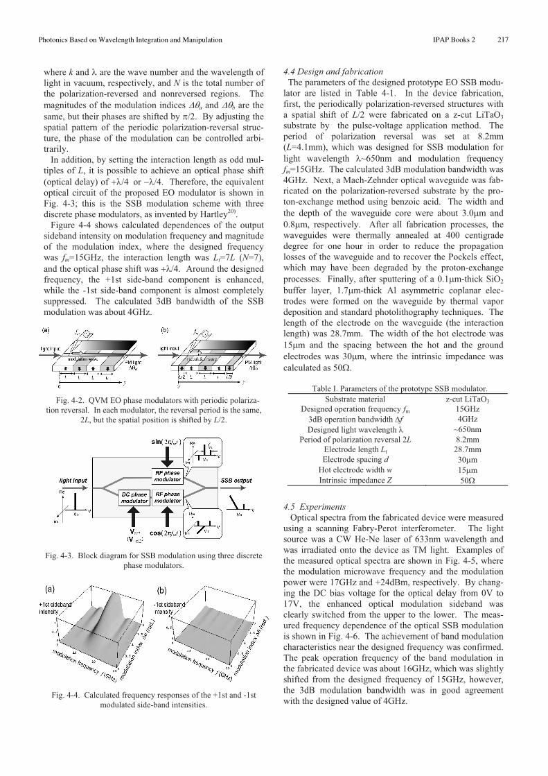
4.2 Structure and operation principle
The basic device structure of the proposed EO SSB
guided-wave modulator is shown in Fig. 4-1. It consists of
a Mach-Zehnder waveguide and traveling-wave electrodes
fabricated on a periodically polarization-reversed ferro-
electric material substrate. LiNbO3, LiTaO3, or KNbO3 are
applicable for the ferroelectric material substrate. Two
periodically polarization-reversed structures for the QVM
are formed along two straight optical waveguides of a
Mach-Zehnder interferometer. The polarization-reversal
periods are the same, 2L, in the two guides, however, pat-
terns of reversal are spatially shifted by a quarter period,
L/2, relative to each other. The length of the reversed and
nonreversed region, L, is determined using equation (2-1).
We have found that the modulation phase in QVM EO
modulation with the periodic polarization reversal is con-
trollable by shifting the spatial position of the periodically
polarization-reversal structure along the propagation direc-
tion. Utilizing this interesting feature, balanced modula-
tion characteristics with a quadrature phase shift are ob-
tained in the two arms of the Mach-Zehnder waveguide
when the proposed device is driven by a RF modulation
signal near the designed frequency. Adjusting the elec-
trode length to be a moderate length, an optical quarter-
wavelength delay between the two arms is also obtained by
supplying a DC voltage between the electrodes. In this
manner, the EO SSB modulation characteristics are ob-
tained [P3, P6, P8].
By using an X-junction waveguide for the Y-junction
waveguide of the output side of the Mach-Zehnder inter-
ferometer, both upper single-sideband (USB) modulated
light and lower single-sideband (LSB) modulated light can
be obtained at the same time.
Fig. 4-1. Basic structure of the prototype EO SSB modulator
using the polarization-reversal scheme.
4.3 Analysis
In Fig. 4-1, the lightwave propagating in each straight
waveguide of the Mach-Zehnder interferometer is modu-
lated at the same time by the RF modulation wave travel-
ing along the electrodes. Each waveguide has the periodi-
cally polarization-reversed structure with the same period
but a spatial shift of L/2. They correspond to the EO phase
modulator shown in Fig. 4-2. The modulation indices in
these two phase modulators are analyzed.
In the traveling-wave modulators, the electrically in-
duced index change that the light sees at point y, n(y, t0),
through the EO effect is expressed as follows.
(4-1)
where nm is the maximum index change by an electric
field, t0 is the time when the light is incident at the edge of
the electrode, and L is defined by equation (2-1). There-
fore, the modulation indices of the light from the two EO
phase modulators in Fig. 4-2 are calculated as follows.
(4-2)
(4-3)
]/2sin[
}]/)/{(2sin[),(
0
00
Lytfn
vyvytfntyn
mm
mgmm
)2cos(4
),()1(
),(),(
0
)1(
0
1
0
2
00
tfLnN
dyktyn
dyktyndyktyn
mm
LN
LN
N
L L
L
a
)2sin(4
),()1(
),()1(
),(),(
0
2/)12(
0
1
2/)12(
2/)32(
0
2/
0
2/3
2/
00
tfLnN
dyktyn
dyktyn
dyktyndyktyn
mm
LN
LN
N
LN
LN
N
L L
L
b
216 Photonics Based on Wavelength Integration and Manipulation IPAP Books 2
where k and are the wave number and the wavelength of
light in vacuum, respectively, and N is the total number of
the polarization-reversed and nonreversed regions. The
magnitudes of the modulation indices a and b are the
same, but their phases are shifted by /2. By adjusting the
spatial pattern of the periodic polarization-reversal struc-
ture, the phase of the modulation can be controlled arbi-
trarily.
In addition, by setting the interaction length as odd mul-
tiples of L, it is possible to achieve an optical phase shift
(optical delay) of or . Therefore, the equivalent
optical circuit of the proposed EO modulator is shown in
Fig. 4-3; this is the SSB modulation scheme with three
discrete phase modulators, as invented by Hartley20).
Figure 4-4 shows calculated dependences of the output
sideband intensity on modulation frequency and magnitude
of the modulation index, where the designed frequency
was fm=15GHz, the interaction length was Lt=7L (N=7),
and the optical phase shift was . Around the designed
frequency, the +1st side-band component is enhanced,
while the -1st side-band component is almost completely
suppressed. The calculated 3dB bandwidth of the SSB
modulation was about 4GHz.
Fig. 4-2. QVM EO phase modulators with periodic polariza-
tion reversal. In each modulator, the reversal period is the same,
2L, but the spatial position is shifted by L/2.
Fig. 4-3. Block diagram for SSB modulation using three discrete
phase modulators.
Fig. 4-4. Calculated frequency responses of the +1st and -1st
modulated side-band intensities.
4.4 Design and fabrication
The parameters of the designed prototype EO SSB modu-
lator are listed in Table 4-1. In the device fabrication,
first, the periodically polarization-reversed structures with
a spatial shift of L/2 were fabricated on a z-cut LiTaO3
substrate by the pulse-voltage application method. The
period of polarization reversal was set at 8.2mm
(L=4.1mm), which was designed for SSB modulation for
light wavelength ~650nm and modulation frequency
fm=15GHz. The calculated 3dB modulation bandwidth was
4GHz. Next, a Mach-Zehnder optical waveguide was fab-
ricated on the polarization-reversed substrate by the pro-
ton-exchange method using benzoic acid. The width and
the depth of the waveguide core were about 3.0 m and
0.8 m, respectively. After all fabrication processes, the
waveguides were thermally annealed at 400 centigrade
degree for one hour in order to reduce the propagation
losses of the waveguide and to recover the Pockels effect,
which may have been degraded by the proton-exchange
processes. Finally, after sputtering of a 0.1 m-thick SiO2
buffer layer, 1.7 m-thick Al asymmetric coplanar elec-
trodes were formed on the waveguide by thermal vapor
deposition and standard photolithography techniques. The
length of the electrode on the waveguide (the interaction
length) was 28.7mm. The width of the hot electrode was
15 m and the spacing between the hot and the ground
electrodes was 30 m, where the intrinsic impedance was
calculated as 50 .
Table I. Parameters of the prototype SSB modulator.
Substrate material z-cut LiTaO3
Designed operation frequency fm 15GHz
3dB operation bandwidth f 4GHz
Designed light wavelength ~650nm
Period of polarization reversal 2L 8.2mm
Electrode length Lt 28.7mm
Electrode spacing d 30 m
Hot electrode width w 15 m
Intrinsic impedance Z 50
4.5 Experiments
Optical spectra from the fabricated device were measured
using a scanning Fabry-Perot interferometer. The light
source was a CW He-Ne laser of 633nm wavelength and
was irradiated onto the device as TM light. Examples of
the measured optical spectra are shown in Fig. 4-5, where
the modulation microwave frequency and the modulation
power were 17GHz and +24dBm, respectively. By chang-
ing the DC bias voltage for the optical delay from 0V to
17V, the enhanced optical modulation sideband was
clearly switched from the upper to the lower. The meas-
ured frequency dependence of the optical SSB modulation
is shown in Fig. 4-6. The achievement of band modulation
characteristics near the designed frequency was confirmed.
The peak operation frequency of the band modulation in
the fabricated device was about 16GHz, which was slightly
shifted from the designed frequency of 15GHz, however,
the 3dB modulation bandwidth was in good agreement
with the designed value of 4GHz.
217Photonics Based on Wavelength Integration and Manipulation IPAP Books 2
4.6 Summary
The novel EO SSB modulator was proposed and its ba-
sic operations were demonstrated. The operation band-
width of the proposed device can be enlarged over several-
fold by using the chirped periodic polarization-reversal
structure[P8]. The applications of the fabricated SSB modu-
lator to radio-on-fiber systems are presented in the next
section.
LSB
-1st sideband
USB
+1st sideband
carrier
17GHz17GHz
LSB
-1st sideband
USB
+1st sideband
carrier
17GHz17GHz
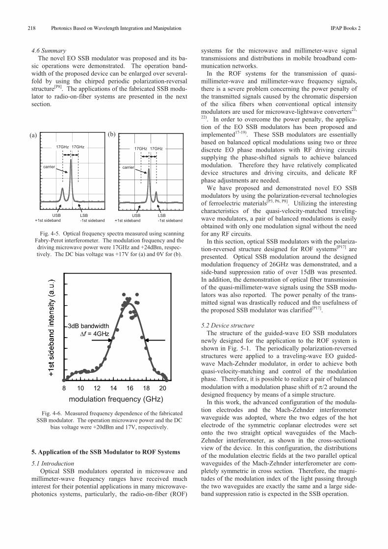
Fig. 4-5. Optical frequency spectra measured using scanning
Fabry-Perot interferometer. The modulation frequency and the
driving microwave power were 17GHz and +24dBm, respec-
tively. The DC bias voltage was +17V for (a) and 0V for (b).
8 10 12 14 16 18 20
modulation frequency (GHz)
3dB bandwidth
f = 4GHz
Fig. 4-6. Measured frequency dependence of the fabricated
SSB modulator. The operation microwave power and the DC
bias voltage were +20dBm and 17V, respectively.
5. Application of the SSB Modulator to ROF Systems
5.1 Introduction
Optical SSB modulators operated in microwave and
millimeter-wave frequency ranges have received much
interest for their potential applications in many microwave-
photonics systems, particularly, the radio-on-fiber (ROF)
systems for the microwave and millimeter-wave signal
transmissions and distributions in mobile broadband com-
munication networks.
In the ROF systems for the transmission of quasi-
millimeter-wave and millimeter-wave frequency signals,
there is a severe problem concerning the power penalty of
the transmitted signals caused by the chromatic dispersion
of the silica fibers when conventional optical intensity
modulators are used for microwave-lightwave converters21,
22). In order to overcome the power penalty, the applica-
tion of the EO SSB modulators has been proposed and
implemented17-19). These SSB modulators are essentially
based on balanced optical modulations using two or three
discrete EO phase modulators with RF driving circuits
supplying the phase-shifted signals to achieve balanced
modulation. Therefore they have relatively complicated
device structures and driving circuits, and delicate RF
phase adjustments are needed.
We have proposed and demonstrated novel EO SSB
modulators by using the polarization-reversal technologies
of ferroelectric materials[P3, P6, P8]. Utilizing the interesting
characteristics of the quasi-velocity-matched traveling-
wave modulators, a pair of balanced modulations is easily
obtained with only one modulation signal without the need
for any RF circuits.
In this section, optical SSB modulators with the polariza-
tion-reversed structure designed for ROF systems[P17] are
presented. Optical SSB modulation around the designed
modulation frequency of 26GHz was demonstrated, and a
side-band suppression ratio of over 15dB was presented.
In addition, the demonstration of optical fiber transmission
of the quasi-millimeter-wave signals using the SSB modu-
lators was also reported. The power penalty of the trans-
mitted signal was drastically reduced and the usefulness of
the proposed SSB modulator was clarified[P17].
5.2 Device structure
The structure of the guided-wave EO SSB modulators
newly designed for the application to the ROF system is
shown in Fig. 5-1. The periodically polarization-reversed
structures were applied to a traveling-wave EO guided-
wave Mach-Zehnder modulator, in order to achieve both
quasi-velocity-matching and control of the modulation
phase. Therefore, it is possible to realize a pair of balanced
modulation with a modulation phase shift of /2 around the
designed frequency by means of a simple structure.
In this work, the advanced configuration of the modula-
tion electrodes and the Mach-Zehnder interferometer
waveguide was adopted, where the two edges of the hot
electrode of the symmetric coplanar electrodes were set
onto the two straight optical waveguides of the Mach-
Zehnder interferometer, as shown in the cross-sectional
view of the device. In this configuration, the distributions
of the modulation electric fields at the two parallel optical
waveguides of the Mach-Zehnder interferometer are com-
pletely symmetric in cross section. Therefore, the magni-
tudes of the modulation index of the light passing through
the two waveguides are exactly the same and a large side-
band suppression ratio is expected in the SSB operation.
(a) (b)
218 Photonics Based on Wavelength Integration and Manipulation IPAP Books 2
Fig. 5-1. Structure of EO SSB modulators for 26GHz ROF sys-
tem applications.
5.3 Fabrication and experiments
The fabrication processes are essentially the same as
those for the device presented in the previous section. The
period of polarization reversal, 2L, was set to be 4.88mm
for the optimum modulation frequency of 26GHz and the
light wavelength of 1.3~1.55 m. The width and the depth
of the proton-exchanged waveguide, which was designed
to be a single-mode guide for lightwave of 1.3~1.55 m,
were set to 4 m and 1.2 m, respectively. The electrode
length, the width of the hot electrode, and the electrode
gaps were 29.28mm, 30 m and 22 m, respectively. In this
device, the intrinsic impedance of the electrodes was de-
signed to be 40 in order to have relatively small electrode
gaps and to realize low driving microwave power. After
all fabrication processes, the waveguides were thermally
annealed at 400 centigrade degree for one hour in order to
reduce the propagation losses of the waveguide and to re-
cover the Pockels effect.
Examples of the modulated light spectra measured using
an optical spectrum analyzer are shown in Fig. 5-2, where
the modulation frequency and the input power were
26GHz and +23dBm, respectively. By changing the DC
bias voltage, the optical sideband component was clearly
switched between the upper and lower ones. The meas-
ured sideband suppression ratio was over 15dB.
An example of the measured frequency dependence of
the fabricated modulators is shown in Fig.6-3. The band
modulation operations around the designed frequency of
26GHz were confirmed. We believe that the dip in the
frequency response at 23GHz was due to the microwave
resonance mode in the LiTaO3 substrate13); it can be elimi-
nated by adjusting the substrate thickness or width, which
was confirmed by calculation using microwave simulators.
Table II. Parameters of the SSB modulator for the ROF system.
Substrate material z-cut LiTaO3
Designed operation frequency fm 26GHz
3dB operation bandwidth f 6GHz
Designed light wavelength 1300~1550nm
Period of domain-inversion 2L 4.88mm
Electrode length Lt 29.28mm
Electrode spacing d 22 m
Hot electrode width w 30 m
Intrinsic impedance Z 40
Single-mode silica fibers and microwave K-connectors
were connected and fixed to both ends of the Mach-
Zehnder waveguide and the coplanar electrodes of the fab-
ricated modulators, respectively. Then, the SSB modulator
module as shown in Fig. 5-4 was fabricated for the ROF
system experiments.
Fig. 5-2. Modulated light spectra from the fabricated SSB modu-
lator. The modulation frequency and the input power were
26GHz and +23dBm, respectively. The DC voltage was -5V for
(a) and 40V for (b).
Fig. 5-3. Measured frequency dependence of the fabricated EO
SSB modulator.
(a)
(b)
219Photonics Based on Wavelength Integration and Manipulation IPAP Books 2
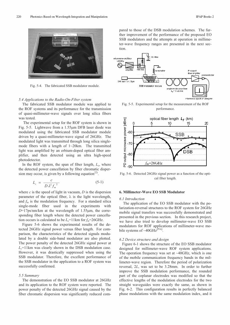
Fig. 5-4. The fabricated SSB modulator module.
5.4 Applications to the Radio-On-Fiber system
The fabricated SSB modulator module was applied to
the ROF systems and its performance for the transmission
of quasi-millimeter-wave signals over long silica fibers
was tested.
The experimental setup for the ROF system is shown in
Fig. 5-5. Lightwave from a 1.55 m DFB laser diode was
modulated using the fabricated SSB modulator module
driven by a quasi-millimeter-wave signal of 26GHz. The
modulated light was transmitted through long silica single-
mode fibers with a length of 1~20km. The transmitted
light was amplified by an erbium-doped optical fiber am-
plifier, and then detected using an ultra high-speed
photodetector.
In the ROF system, the span of fiber length, Lc, where
the detected power cancellation by fiber chromatic disper-
sion may occur, is given by a following equation22).
(5-1)
where c is the speed of light in vacuum, D is the dispersion
parameter of the optical fiber, is the light wavelength,
and fm is the modulation frequency. For a standard silica
single-mode fiber used in the experiments with
D=17ps/nm/km at the wavelength of 1.55 m, the corre-
sponding fiber length where the detected power cancella-
tion occurs is calculated to be Lc=11km for fm=26GHz.
Figure 5-6 shows the experimental results of the de-
tected 26GHz signal power versus fiber length. For com-
parison, the characteristics of the detected signals modu-
lated by a double side-band modulator are also plotted.
The power penalty of the detected 26GHz signal power at
Lc=11km was clearly shown in the DSB modulation case.
However, it was drastically suppressed when using the
SSB modulator. Therefore, the excellent performance of
the SSB modulator in the application to a ROF system was
successfully confirmed.
5.5 Summary
The demonstration of the EO SSB modulator at 26GHz
and its application to the ROF system were reported. The
power penalty of the detected 26GHz signal caused by the
fiber chromatic dispersion was significantly reduced com-
pared to those of the DSB modulation schemes. The fur-
ther improvement of the performance of the proposed EO
SSB modulators and the attempts at operation in millime-
ter-wave frequency ranges are presented in the next sec-
tion.
Fig. 5-5. Experimental setup for the measurement of the ROF
performance.
Fig. 5-6. Detected 26GHz signal power as a function of the opti-
cal fiber length.
6. Millimeter-Wave EO SSB Modulator
6.1 Introduction
The application of the EO SSB modulator with the po-
larization-reversal structures to the ROF system for 26GHz
mobile signal transfers was successfully demonstrated and
presented in the previous section. In this research project,
we have also tried to develop millimeter-wave EO SSB
modulators for ROF applications of millimeter-wave mo-
bile systems of ~40GHz[P16].
6.2 Device structure and design
Figure 6-1 shows the structure of the EO SSB modulator
designed for millimeter-wave ROF system applications.
The operation frequency was set at ~40GHz, which is one
of the mobile communication frequency bands in the mil-
limeter-wave region. Therefore the period of polarization
reversal, 2L, was set to be 3.28mm. In order to further
improve the SSB modulation performance, the rounded
part of the coplanar electrodes was modified so that the
effective lengths of the modulation electrodes for the two
straight waveguides were exactly the same, as shown in
Fig. 6-2. This configuration results in perfectly balanced
phase modulations with the same modulation index, and it
22
m
cfD
cL
220 Photonics Based on Wavelength Integration and Manipulation IPAP Books 2
is expected to exhibit a higher sideband suppression ratio
in SSB modulation compared to the previous devices pre-
sented in sections 4 and 5. In addition, in order to reduce
the DC bias voltage for the control of optical bias, a nonpe-
riodic polarization-reversed region was defined as shown
in Fig. 6-1. The length of the nonperiodic region was ad-
justed to be an integer multiple of the polarization period,
2nL (n: integer), therefore, millimeter-wave modulation
characteristics were not affected by this region.
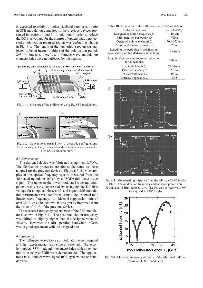
Fig. 6-1. Structure of the millimeter-wave EO SSB modulators.
Fig. 6-2. Conventional (a) and new (b) electrode configurations
for achieving perfectly balanced modulation characteristics and a
high SSB extinction ratio.
6.3 Experiments
The designed device was fabricated using z-cut LiTaO3.
The fabrication processes are almost the same as those
adopted for the previous devices. Figure 6-3 shows exam-
ples of the optical frequency spectra measured from the
fabricated modulator driven by a 38GHz millimeter-wave
signal. The upper or the lower modulated sideband com-
ponent was clearly suppressed by changing the DC bias
voltage for an optical phase shift, and a good SSB modula-
tion performance was confirmed around the designed mil-
limeter-wave frequency. A sideband suppression ratio of
over 30dB was obtained, which was greatly improved from
the value of 15dB of the previous device.
The measured frequency dependence of the SSB modula-
tor is shown in Fig. 6-4. The peak modulation frequency
was shifted to slightly higher than the designed value of
40GHz. However, the 3dB operation bandwidth, 6GHz,
was in good agreement with the designed one.
6.4 Summary
The millimeter-wave EO SSB modulators were designed
and their experimental results were presented. The excel-
lent optical SSB modulation characteristics with an extinc-
tion ratio of over 30dB were demonstrated. The applica-
tions to millimeter-wave signal ROF systems are now un-
der way.
Table III. Parameters of the millimeter-wave SSB modulator.
Substrate material z-cut LiTaO3
Designed operation frequency fm ~40GHz
3dB operation bandwidth f 7GHz
Designed light wavelength 1300~1550nm
Period of domain-inversion 2L 3.28mm
Length of the periodically polarization-reversed region for MM-wave modulation
19.68mm
Length of the polarization-reversed region for optical bias
9.84mm
Electrode length Lt 29.52mm
Electrode spacing d 22 m
Hot electrode width w 36 m
Intrinsic impedance Z 30
Fig. 6-3. Modulated light spectra from the fabricated SSB modu-
lator. The modulation frequency and the input power were
38GHz and 18dBm, respectively. The DC bias voltage was 1.9V
for (a), and +14.8V for (b).
Fig. 6-4. Measured frequency response of the fabricated millime-
ter-wave EO SSB modulator.
(a)
(b)
(a) (b)
221Photonics Based on Wavelength Integration and Manipulation IPAP Books 2
7. EO Optical Frequency Shifter
7.1 Introduction
An optical frequency shifter (OFS) is an important de-
vice in many optoelectronics applications: for example,
optical fiber communication systems, particularly wave-
length division multiplexing (WDM) systems for precise
control of the laser frequency to the grid ones; optical sig-
nal processing systems; optical measurements for hetero-
dyne detections; laser spectroscopy; laser cooling; and
photochemistry. However, the operation frequency of a
commercially available OFS using acoustooptic effects is
in the range of several hundred MHz. Therefore, a high-
speed OFS with the operation frequency exceeding the
GHz range is expected in many application fields.
We have proposed a novel EO high-speed OFS/carrier
suppressed SSB modulator that has a new guided-wave
optical circuit, which we named the “3-branch waveguide
interferometer” and the polarization-reversal technology of
ferroelectric materials[P18]. This OFS is compact and can
be operated in very high frequency range (1~100GHz)
with one RF modulation signal and DC bias voltages. A
continuous sweep of optical frequency over a range of sev-
eral GHz is possible, and the direction of frequency shift
(upward or downward) can be switched by tuning the bias
voltage. In this section, the operation principle, analysis,
and demonstration are presented.
7.2 Structure and operation principle
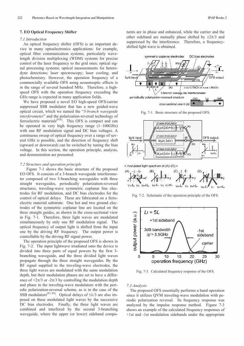
Figure 7-1 shows the basic structure of the proposed
EO OFS. It consists of a 3-branch waveguide interferome-
ter composed of two 3-branching waveguides with three
straight waveguides, periodically polarization-reversed
structures, traveling-wave symmetric coplanar line elec-
trodes for RF modulation, and DC bias electrodes for the
control of optical delays. These are fabricated on a ferro-
electric material substrate. One hot and two ground elec-
trodes of the symmetric coplanar line are located on the
three straight guides, as shown in the cross-sectional view
in Fig. 7-1. Therefore, three light waves are modulated
simultaneously by only one RF modulation signal. The
optical frequency of output light is shifted from the input
one by the driving RF frequency. The output power is
controllable by the driving RF signal power.
The operation principle of the proposed OFS is shown in
Fig. 7-2. The input lightwave irradiated onto the device is
divided into three parts of equal powers by the first 3-
branching waveguide, and the three divided light waves
propagate through the three straight waveguides. By the
RF signal supplied to the traveling-wave electrodes, the
three light waves are modulated with the same modulation
depth, but their modulation phases are set to have a differ-
ence of +2 /3 or -2 /3 by controlling the modulation depth
and phase in the traveling-wave modulators with the peri-
odic polarization-reversal scheme, as is in the case of the
SSB modulators[P3, P8]. Optical delays of /3 are also im-
posed on these modulated light waves by the successive
DC bias electrodes. Finally, the three light waves are
combined and interfered by the second 3-branching
waveguide, where the upper (or lower) sideband compo-
nents are in phase and enhanced, while the carrier and the
other sideband are mutually phase shifted by 2 /3 and
suppressed by the interference. Therefore, a frequency-
shifted light wave is obtained.
Fig. 7-1. Basic structure of the proposed OFS.
Fig. 7-2. Schematic of the operation principle of the OFS.
Fig. 7-3. Calculated frequency response of the OFS.
7.3 Analysis
The proposed OFS essentially performs a band operation
since it utilizes QVM traveling-wave modulation with pe-
riodic polarization reversal. Its frequency response was
analyzed by the impulse response method. Figure 7-3
shows an example of the calculated frequency responses of
+1st and -1st modulation sidebands under the appropriate
222 Photonics Based on Wavelength Integration and Manipulation IPAP Books 2
optical delays. In this case, the +1st modulation sideband
component was enhanced, and the carrier and the -1st side-
band were almost completely suppressed.
The light propagation characteristics of the 3-branching
waveguides were also analyzed using the BPM. The pa-
rameters of the 3-branch waveguide for dividing light
waves into three parts of equal powers were determined in
the analysis and the 3-branch waveguide interferometer
was designed.
7.4 Experiments
The fabrication processes are essentially the same as
those adopted for the device presented in the previous sec-
tions. Z-cut LiTaO3 was used as the substrate material.
The period of polarization reversal, 2L, was set to be
8.2mm, which was designed for the operation of light
waves of ~650nm and the operation frequency of 15GHz.
The 3-branch waveguide interferometer was fabricated by
the proton-exchange method with benzoic acid. In the 3-
branching waveguides, the width of the waveguide was set
to be 3.3 m for the center guide and 4.2 m for the outer
two guides, and the branching angle between the center
and the outer waveguides was 1/200rad. These parameters
were determined by BPM analysis in order to have the
exactly equal power splitting ratio. The length of the RF
modulation electrodes, Lt, was set to be 20.5mm (5L).
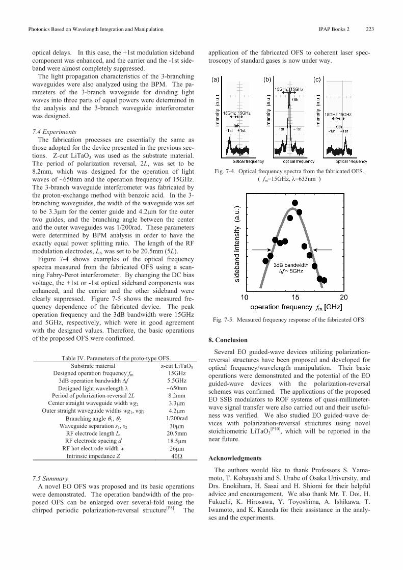
Figure 7-4 shows examples of the optical frequency
spectra measured from the fabricated OFS using a scan-
ning Fabry-Perot interferometer. By changing the DC bias
voltage, the +1st or -1st optical sideband components was
enhanced, and the carrier and the other sideband were
clearly suppressed. Figure 7-5 shows the measured fre-
quency dependence of the fabricated device. The peak
operation frequency and the 3dB bandwidth were 15GHz
and 5GHz, respectively, which were in good agreement
with the designed values. Therefore, the basic operations
of the proposed OFS were confirmed.
Table IV. Parameters of the proto-type OFS.
Substrate material z-cut LiTaO3
Designed operation frequency fm 15GHz
3dB operation bandwidth f 5.5GHz
Designed light wavelength ~650nm
Period of polarization-reversal 2L 8.2mm
Center straight waveguide width wg2 3.3 m
Outer straight waveguide widths wg1, wg3 4.2 m
Branching angle 1/200rad
Waveguide separation s1, s2 30 m
RF electrode length Lt 20.5mm
RF electrode spacing d 18.5 m
RF hot electrode width w 26 m
Intrinsic impedance Z 40
7.5 Summary
A novel EO OFS was proposed and its basic operations
were demonstrated. The operation bandwidth of the pro-
posed OFS can be enlarged over several-fold using the
chirped periodic polarization-reversal structure[P8]. The
application of the fabricated OFS to coherent laser spec-
troscopy of standard gases is now under way.
Fig. 7-4. Optical frequency spectra from the fabricated OFS.
( fm=15GHz, =633nm )
Fig. 7-5. Measured frequency response of the fabricated OFS.
8. Conclusion
Several EO guided-wave devices utilizing polarization-
reversal structures have been proposed and developed for
optical frequency/wavelength manipulation. Their basic
operations were demonstrated and the potential of the EO
guided-wave devices with the polarization-reversal
schemes was confirmed. The applications of the proposed
EO SSB modulators to ROF systems of quasi-millimeter-
wave signal transfer were also carried out and their useful-
ness was verified. We also studied EO guided-wave de-
vices with polarization-reversal structures using novel
stoichiometric LiTaO3[P10], which will be reported in the
near future.
Acknowledgments
The authors would like to thank Professors S. Yama-
moto, T. Kobayashi and S. Urabe of Osaka University, and
Drs. Enokihara, H. Sasai and H. Shiomi for their helpful
advice and encouragement. We also thank Mr. T. Doi, H.
Fukuchi, K. Hirosawa, Y. Toyoshima, A. Ishikawa, T.
Iwamoto, and K. Kaneda for their assistance in the analy-
ses and the experiments.
223Photonics Based on Wavelength Integration and Manipulation IPAP Books 2

References
1) K. K. Wong ed.: Lithium Niobate (IEE, London, 2002).
2) G. E. Betts, RF Photonic Technology in Optical Fiber Links, ed. W. S.
C. Chang (Cambridge University Press, Cambridge, 2002) Chap. 4,
p.81.
3) K. Yamamoto, K. Mizuuchi, K. Takeshige, Y. Sasai, and T. Taniuchi:
J. Appl. Phys., 70 (1991) 1947.
4) M. Fujimura, K. Kintaka, T. Suhara, and H. Nishihara: Electron. Lett.,
28 (1992) 1868.
5) M. Yamada, N. Nada, M. Saitoh, and K. Watanabe: Appl. Phys. Lett.,
62 (1993) 435.
6) A. Harada, Y. Nihei, Y. Okazaki, and H. Hyuga: Opt. Lett., 22 (1997)
805.
7) G. D. Miller, R. G. Batchko, W. M. Tulloch, D. R. Weise, M. M. Fejer,
and L. Byer: Opt. Lett., 22 (1997) 1834.
8) M. A. Arbore, M. M. Fejer: Opt. Lett., 22 (1997) 151.
9) M. Sato, T. Hatanaka, S. Izumi, T. Taniuchi, and H. Ito: Appl. Opt., 38
(1999) 2560.
10) H. Murata, A. Morimoto, T. Kobayashi, and S. Yamamoto: IEEE J.
Select. Topics Quantum Electron., 6 (2000) 1325.
11) H. Murata, K. Kinoshita, G. Miyaji, A. Morimoto, and T. Kobayashi:
Electron. Lett., 36 (2000) 1459.
12) W. Wang, R. Tavlykaev, and R. V. Ramaswamy : IEEE Photon. Tech.
Lett., 9 (1997) 610.
13) M. M. Howerton and W. K. Burns, RF Photonic Technology in Opti-
cal Fiber Links, ed. W. S. C. Chang (Cambridge University Press,
Cambridge, 2002) Chap. 5, p.133.
14) M. Sugiyama, M. Doi, T. Nakazawa: Optical Fiber Communication
Conference 2002, PD FB6 (2002)
15) G. K. Gopalakrishnan, W.K.Burns, R. W. McElhanon, C. H. Bulmer,
and A. S. Greenblatt: J. Lightwave Technol., 12 (1994) 1807.
16) K. Noguchi, O. Mitomi, and H. Miyazawa: J. Lightwave Technol., 16
(1998) 615.
17) M. Izutsu, S. Shikama, T. Sueta: IEEE J. Quantum Electron., QE-17
(1981) 2225.
18) S. Shimotsu, S. Oikawa, T. Saitou, N. Mitsugi, K. Kubodera, T. Ka-
wanishi, M. Izutsu: IEEE Photon. Technol. Lett., 13 (2001) 364.
19) A. Loayssa, D. Benito, and M. J. Garde: IEEE Photon. Technol. Lett.,
13 (2001) 869.
20) R.Hartley : U.S. Patent 1666206 (1928).
21) G. H. Smith, D. Novak, Z. Ahmed: Electron. Lett., 33 (1997) 74.
22) G. H. Smith, D. Novak: IEEE Trans. Microwave Theory & Tech., 45,
(1997) 1410.
Publications
Journal papers
[P1] H. Murata, A. Morimoto, T. Kobayashi, and S. Yamamoto: “Optical
pulse generation by using quasi-velocity-matched guided-wave elec-
trooptic phase modulator,” Optical and Quantum Electronics, vol.33,
pp.785-794 (July 2001)
[P2] A. Enokihara, H. Yajima, M. Kosaki, H. Murata and Y. Okamura:
“Guided-wave electro-optic modulator using resonant electrode of
coupled microstrip lines,” Electron.Lett., vol.39, pp.1671-1673 (Nov.
2003).
[P3] H. Murata, and Y. Okamura: “Guided-wave electro-optic single side-
band modulators by use of polarization-reversed structures,” The Re-
view of Laser Engineering (in Japanese), vol. 32, No. 3, pp.186-190
(March, 2004).
[P4] A. Ishikawa, H. Murata, T. Tanaka, H. Shiomi, Y. Okamura, and S.
Yamamoto: “Positive and Negative Optical Responses in High-
Electron Mobility Transistors and Their Applications to Optically
Controlled Microwave Oscillators,” Japanese Journal of Applied
Physics, vol.43, No.3, pp.997-1001 (March, 2004).
International conferences
[P5] H.Murata, H. Fukuchi, K. Kinoshita, A. Morimoto, T. Kobayashi,
and S. Yamamoto: “Quasi-velocity-matched guided-wave optical
modulator with resonant electrodes for integrated ultrashort pulse
generators,” The Conference on Lasers and Electro-Optics 2001
(CLEO2001), Baltimore, CThL10, pp.442-443 (May 10, 2001).
[P6] H. Murata, T. Doi, T. Kobayashi, and S. Yamamoto: “Novel elec-
trooptic SSB modulator/optical frequency shifter using periodically
domain-inverted structure,” The 4th Pacific Rim Conference on La-
sers and Electro-Optics (CLEO/Pacific Rim2001), Chiba, ME2-5,
Vol.1, pp.106-107 (July 16, 2001).
[P7] H. Murata, H. Fukuchi, T. Doi, T. Kobayashi, and S. Yamamoto:
“Guided-wave electrooptic LiTaO3 modulators using domain-inverted
structure,” The 2nd International Laser, Lightwave and Microwave
Conference (ILLMC2001), Shanghai, pp.133-135, H-2 (November 7,
2001).
[P8] H. Murata, T. Doi, T. Kobayashi, and S. Yamamoto: “Novel guided-
wave single-sideband electrooptic modulators by using periodically
domain-inverted structure,” The Conference on Lasers and Electro-
Optics 2002 (CLEO2002), Long Beach, CTuK14, pp.204-205 (May
21, 2002).
[P9] H. Murata, T. Doi, K. Hirosawa, and S. Yamamoto: “Optical single-
sideband modulation by using periodically domain-inverted LiTaO3
guided-wave modulators,” The Microwave Photonics Conference
2002 (MWP2002), Hyogo, W4-3, pp.53-56 (November 6, 2002).
[P10] A. Ishikawa, H. Murata, and S. Yamamoto: “Quasi-velocity-
matched guided-wave electrooptic modulator by using stoichiometric
domain-inverted LiTaO3,” The sixth International Topical Workshop
on Contemporary Photonic Technologies (CPT2003), Tokyo, PDP-5,
p.5 (January 16, 2003).
[P11] H. Murata and S. Yamamoto: “Optical modulator with polarization-
reversed structures (invited talk),” The 1st NIMS International Con-
ference -Material Solutions for Photonics-, Tsukuba, II-11, pp.45-46
(March 18, 2003).
[P12] H. Murata, S. Yamamoto, H. Sasai, and A. Enokihara: “Novel
guided-wave electrooptic single-sideband modulator by using peri-
odically domain-inverted structure for a long wavelength operation,”
The Optical Fiber Communication Conference 2003 (OFC2003), At-
lanta, MF53 (March 24, 2003).
[P13] H. Murata, K. Kaneda, S. Yamamoto: “Low-power and low-chirp
guided-wave electrooptic intensity modulator by use of domain-
inverted structure,” The Conference on Lasers and Electro-Optics
2003 (CLEO2003), Baltimore, CWA-19 (June 4, 2003).
[P14] H. Murata, K. Hirosawa, S. Yamamoto, H. Sasai, and A. Enokihara:
“26GHz optical single-sideband modulation by using guided-wave
electrooptic modulator with periodically polarization-reversed struc-
tures,” The 10th International Workshop on Femtosecond Technology
(FST2003), Chiba, TP-3, p.152 (July 17, 2003).
[P15] A. Ishikawa, H. Murata, T. Tanaka, H. Shiomi, and S. Yamamoto:
“Positive and negative optical responses in high-electron mobility
transistors and their applications to optically controlled microwave
oscillators,” The 5th Pacific Rim Conference on Lasers and Electro-
Optics (CLEO/Pacific Rim2003), Taipei, THP-(2)-4, p.510 (Decem-
ber 18, 2003).
[P16] H. Murata, K. Kaneda, and Y. Okamura: “38GHz optical single-
sideband modulation by using guided-wave electrooptic modulators
with periodic polarization-reversal,” The Conference on Lasers and
Electro-Optics 2004 (CLEO2004), San Francisco, CThT10 (May 20,
2004).
[P17] H. Murata, Y. Okamura, H. Sasai, and A. Enokihara: “Demonstra-
tion of 26GHz signal optical fiber transmission by use of guided-
wave electrooptic single-sideband modulators with periodically po-
larization-reversed schemes,” The IEEE MTT-S International Micro-
wave Symposium (IMS2004), Fort Worth, Texas, IFTH-60, vol.3,
pp.2059-2062 (June 10, 2004).
[P18] H. Murata, T. Iwamoto, and Y. Okamura: “Novel electrooptic opti-
cal frequency shifters by use of a 3-branch waveguide interferometer
and polarization-reversal structures,” The Ninth Optoelectronics and
Communications Conference/Third International Conference on Op-
tical Internet (OECC/COIN2004), Yokohama, 14F3-3, pp.564-565,
(July 14, 2004).
[P19] H. Murata, and Y. Okamura: “Millimeter-wave electrooptic Single-
Sideband modulators using polarization-reversed structures (invited
talk),” The 8th International Symposium on Ferroic Domains and Mi-
cro- to Nanoscopic Structures (ISFD-8), S08-Thp05, p.20, Tsukuba
(August 26, 2004).
224 Photonics Based on Wavelength Integration and Manipulation IPAP Books 2
Top Related