


Languages
Pages
Legal


FPGA Design and Implementation of Wavelet Coherence forEEG Signals
Author
Qassim, Yahya Taher
Published
2014
Thesis Type
Thesis (PhD Doctorate)
School
School of Engineering
DOI
https://doi.org/10.25904/1912/3626
Copyright Statement
The author owns the copyright in this thesis, unless stated otherwise.
Downloaded from
http://hdl.handle.net/10072/366086
Griffith Research Online
https://research-repository.griffith.edu.au
FPGA Design and
Implementation of Wavelet
Coherence for EEG Signals
Yahya T Qassim
MSc. Eng
School of Engineering
Science, Environment, Engineering and Technology
Griffith University
Brisbane, Australia
Submitted in fulfilment of the requirements of
the degree of Doctor of Philosophy
November 2013
Abstract
The EEG waveform provides millisecond resolution brain information
that can be obtained from the scalp using metal electrodes. It has become an
applicable measure for a wide range of brain functionalities (including higher
cognition) due to its low cost, non-invasiveness and ease of access. An
important EEG application uses an evoked form of these signals linked to an
external stimulus. For this thesis, an EEG was acquired during presentation of
an oddball task and recording the event related potential (ERP), in which the
P300 component is the most important. It reflects the participant’s response
to rare or occasional stimulus events. Extracting features from these non-
stationary signals can be achieved with a time-frequency method such as the
continuous wavelet transform (CWT) whereas examining the functional
connectivity between a pair of brain channels, as a source of EEG, can be
achieved with the wavelet coherence (WC). However, the real time
processing of these two digital signal processing (DSP) algorithms, which
imply a large number of computations, requires running them with minimal
delay for use in real time biofeedback applications.
To achieve the required speed of processing for real time EEG
applications, the involvement of hardware computation is required. One of
the well-known hardware platforms in the field of DSP is the Field
Programmable Gate Array (FPGA). These devices allow digital
implementation of a wide range of DSP algorithms with a high processing
speed, in addition to their configurability and portability. The aim of this
thesis was the FPGA design and implementation of WC for EEG signals.

The algorithm and architecture for the CWT and WC, as well as their
applications to the cognition-based ERP waves, was investigated in this
dissertation due to their validity in analysing time series signals and their
potential value for a proposed biofeedback system based on these
algorithms.
The first phase of this thesis involved developing a novel WC based
method for characterizing and analysing the EEGs measured from the frontal
and central scalp sites under the oddball test. The expectancy hypothesis was
supported through the analysis in the gamma band. The results showed a
significant difference between the EEG trials in the low frequency band and
in the higher frequency gamma band.
In the next phase, a novel architecture was built with a hardware
description language (VHDL) to perform the CWT for EEG signals. It was
implemented on the FPGA, which compares well against previous
implementations in the literature. In the last phase of this thesis, another
novel design was developed and implemented to estimate the WC between
two EEG signals using the same FPGA. The correctness of the FPGA results
was verified against the software results using image quality methods and
showed a high level of accuracy.
A low cost FPGA platform has the ability to compute the assigned
algorithms for both the CWT and the WC applied to a pair of ERP epochs in a
few milliseconds (1.14 ms for the CWT and 8.7 ms for the WC) and provide
the means for EEG monitoring and biofeedback applications. Based on the
design of the WC, a biofeedback technique was derived and proposed for
further study in the field.

Statement of Originality
“This work has not previously been submitted for a degree or diploma in any
university. To the best of my knowledge and belief, the thesis contains no
material previously published or written by another person except where
due reference is made in the thesis itself.”
Signature ________________________________________________________
Yahya T Qassim

TO MY LOVING PARENTS AND WIFE, FOR THEIR
ENCOURAGEMENT AND SUPPORT
Acknowledgments
I would like to express my thanks to my supervisors, Dr. David
Rowlands, Dr. Tim Cutmore and Dr. Daniel James for their guidance, patience,
support and valuable supervision of this work. Thanks David for the
introduced technical support, sincere comments and valuable advice which
helped me in designing the wavelet analysis engines and facilitating the ways
for implementing the required algorithms. Thanks Tim for the valuable
advice and for providing the required EEG data for this research which was
very helpful in the wavelet analysis and in testing the wavelet design within
the FPGA.
I am also grateful to the Centre for Wireless Monitoring and
Applications (CWMA) at Griffith University for providing the research
requirements to complete this work. I would like to thank my colleagues,
Jonathon Neville and Mitchel McCarthy with whom I have discussed thoughts
and shared labs at Griffith University. I am very grateful for the financial
support (sponsorship) from the Ministry of Higher Education and Scientific
Research (MOHSR) of Iraq.
Finally, I would like to express my thanks to my father and mother for
their support and encouragement. Special thanks to my wife, Israa, for her
patience and support during the whole period of my study.

Contents
I
Contents
Glossary of Abbreviations…………………………………………………………….
XV
Glossary of Terms………………………………………………………………………..
XVII
List of Symbols……………………………………………………………………………
XIX
Chapter 1: Introduction……………………………………………………………... 1
1.1 Research Topic…………………………………………………………………… 4
1.2 Thesis Outline …………………………………………………………………….. 5
1.3 Publications ….…………………………………………………………………… 7
1.4 References………………………………………………………………................
9
Chapter 2: The Cognitive System and Electroencephalography.
11
2.1 Neuroelectric Waveform…………………………………………………… 12
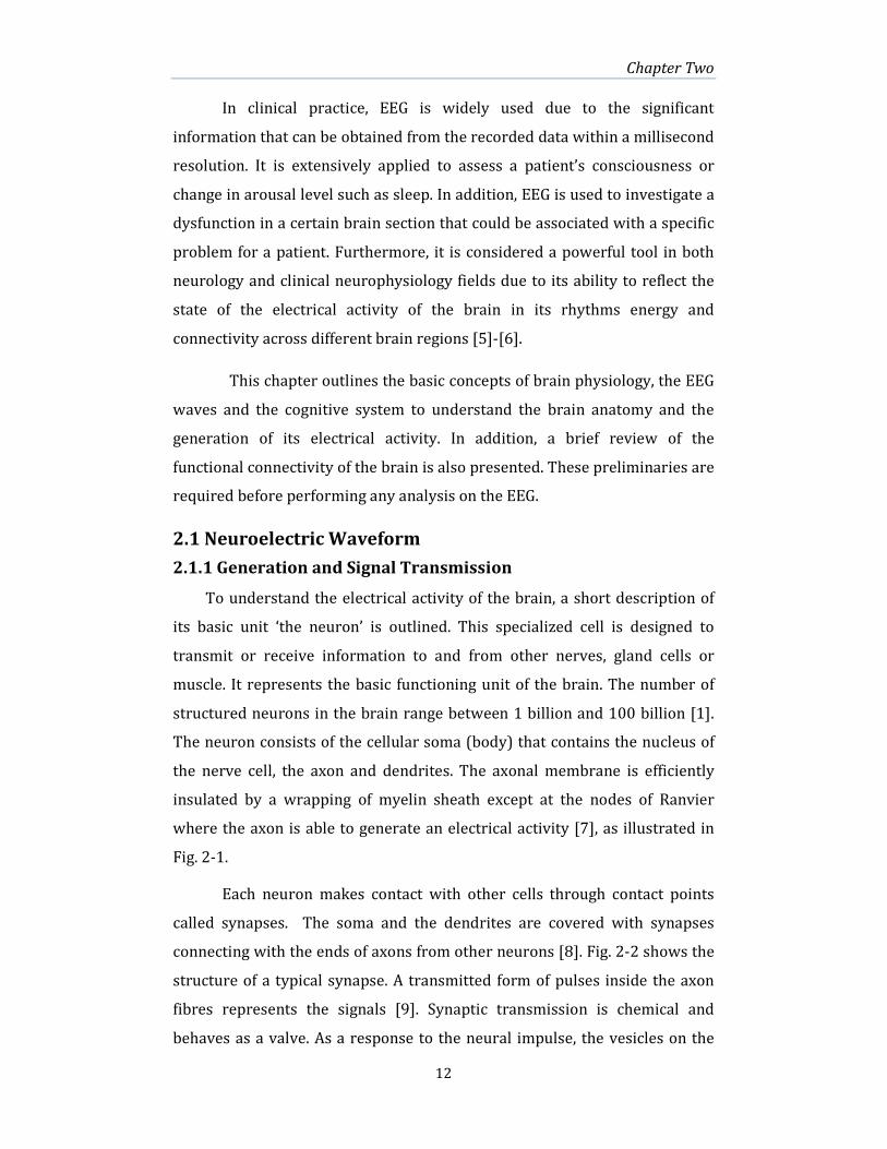
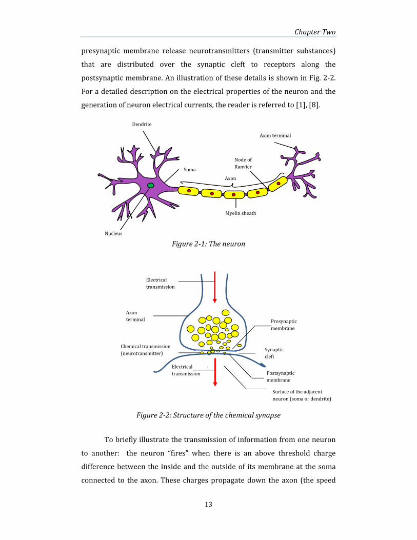
2.1.1 Generation and Signal Transmission………………………… 12
2.1.2 Anatomy of the Brain………………………………………………. 14
2.2 The Electroencephalogram (EEG) & Its Frequency Bands..… 16
2.2.1 Measurement…………………………………………………………... 19
2.2.1.1 Electrode Placement System…………………………. 19
2.2.1.2 Recording…………………………………………………….. 20
2.2.1.3 Noise Sources………………………………………………. 20
2.2.2 The Evoked Potential (EP)……………………………………….. 21
2.2.2.1 The P300……………………………………………………... 24
2.2.2.2 The Oddball Test …………………………………………. 25
2.3 EEG Connectivity Between Brain Regions………………………….. 25
2.4 Summary…………………………………………………………………………. 26
2.5 References………………………………………………………………………..
27
Chapter 3: Theory of Signal Analysis and Applications………….
30
3.1 Fourier Analysis……………………………………………………………….. 32
3.1.1 Fourier Series…………………………………………………………... 32

Contents
II
3.1.2 Fourier Transform (FT)……………………………………………. 33
3.1.2.1 Properties of Fourier Transform……………………. 33
3.1.2.2 Discrete Time Fourier Transform (DTFT)………. 34
3.1.2.3 Discrete Fourier Transform (DFT)…………………. 35
3.1.2.4 Fast Fourier Transform (FFT)………………………… 36
3.1.3 Short-Time Fourier Transform (STFT)……………………….. 37
3.2 Wavelets…………………………………………………………………………… 38
3.2.1 Wavelet Properties…………………………………………………….. 39
3.2.2 The Continuous Wavelet Transform……………………………. 40
3.2.2.1 The Morlet Wavelet Function………………………….. 42
3.2.2.2 FFT Based CWT……………………………………………….. 44
3.2.3 The Discrete Wavelet Transform (DWT)……………………… 46
3.2.4 Coherence Estimation………………………………………………… 47
3.2.4.1 Coherence Measure…………………………………………. 48
3.2.4.2 Magnitude Coherence……………………………………… 48
3.2.4.3 Wavelet Coherence………………………………………….. 49
3.2.4.4 Wavelet Phase Coherence………………………………… 51
3.2.5 Applications of CWT & WC………………………………………….. 52
3.3 Scalogram Quality Measures………………………………………………… 53
3.3.1 Normalized MSE………………………………………………………….. 53
3.3.2 Normalized AD……………………………………………………………. 54
3.3.3 Structural Content (SC)……………………………………………….. 54
3.4 Summary……………………………………………………………………………. 55
3.5 References…………………………………………………………………………..
56
Chapter 4: Hardware Concepts and Architecture ……………………
59
4.1 DSP Platforms…………………………………………………………………. 59
4.1.1 FPGA Structure………………………………………………………. 61
4.1.2 CAD Tools and HDL Design Flow……………………………… 63
4.2 Concepts of Digital Hardware Design………………………………… 65
4.2.1 Word Length Selection…………………………………………….. 66
4.2.2 Design Critical Path and Timing Constraints…………….. 67
4.2.3 Area and Speed……………………………………………………….. 68
4.2.4 Design Optimization………………………………………………… 68
4.3 The Xilinx FFT Core: Configuration and Generation……………. 69
Contents
III
4.3.1 Architectural Options for the FFT IP-Core………………… 72
4.4 FFT Core Control Circuit…………………….……………………………. 75
4.5 Testing……………………………………………………………………………. 78
4.6 Summary…………………………………………………………………………. 81
4.7 References……………………………………………………………………….
83
Chapter 5: Wavelet Coherence of EEG Signals for a Visual
Oddball Task……………………………………………………………………………..
85
5.1 Related Work…………………………………………………………………… 85
5.2 Preliminary Processing and EEG Inspection……………………… 88
5.2.1 Trial Exclusion………………………………………………………… 88
5.2.2 EEG Frequencies……………………………………………………… 89
5.2.3 Noise Mitigation through Averaging…………………………. 90
5.3 Wavelet Analysis……………………………………………………………… 92
5.3.1 Data Acquisition and Test Description ………..…………… 92
5.3.2.1 Results for CWT and WC Analysis…………………. 94
5.3.2.2 Results for Gamma Correlation……………............ 99
5.4 Discussion of Results……………………………………………………….. 105
5.5 Summary…………………………………………………………………………. 108
5.6 References……………………………………………………………………….
109
Chapter 6: FPGA Implementation and Design Optimization of
Morlet CWT for EEG Analysis……………………………………………………
111
6.1 Related Work…………………………………………………………………… 112
6.2 System Model…………………………………………………………………... 112
6.2.1 FFT Based CWT……………………………………………………….. 113
6.2.2 The Wavelet Function Representation……………………… 115
6.2.3 Wavelet Function Based Optimization……………………… 116
6.2.3.1 Lookup Table (LUT)……………………………………… 116
6.2.3.2 Zero Exclusion……………………………………………… 117
6.2.3.3 Multiplications……………………………………………... 117
6.2.4 Morlet Scales and the Corresponding Frequencies……. 119
6.2.4.1 Morlet Wavelet in Fourier Space…………………… 120
6.2.4.2 Corresponding Indices…………………………………. 122
6.3 FPGA Implementation……………………………………………………… 124
6.3.1 Target Technology………………………………………………… 124

Contents
IV
6.3.2 Design Operation……………………………………………………. 125
6.3.2.1 The FFT Core……………………………………………… 127
6.3.2.2 The CWT Controller…………………………………….. 128
6.3.2.3 The Multiplier Controller…………………………….. 129
6.3.2.4 Memory Groups………………………………………….. 133
6.4 Results ………………………………….……………………………………….. 134
6.5 Design Modification & Improvement .……………………………….. 140
6.5.1 Static RAM Controller ……………………….…………………….. 140
6.5.2 Signal Frequency Dependent Optimization……………… 145
6.6 Scalogram Quality Measures…………………………………………….. 150
6.7 Summary & Discussion…………………………………………………… 152
6.8 References……………………………………………………………………….
154
Chapter 7: Wavelet Coherence & Biofeedback: Architecture
and FPGA Implementation……………………………………………………….
156
7.1 Wavelet Coherence System Model…………………………………….. 157
7.1.1 Flow Diagram…………………………………………………………. 160
7.1.2 Software Analysis of wavelet coherence………...………… 162
7.1.2.1 Overflow detection by scalogram analysis…… 163
7.1.2.2 Smoothing…………………………………………………… 167
7.1.2.3 Word Length Selection………………………………… 174
7.2 FPGA Implementation of WC……………………………………………. 178
7.2.1 Design Operation…………………………………………………….. 179
7.2.2 The Wavelet Coherence Processor ………………………….. 190
7.2.3 Results…………………………………………………………………… 191
7.3 FPGA Implementation of WC Based Biofeedback……………… 197
7.4 Summary & Discussion……………………………………………………. 204
7.5 References………………………………………………………………………
206
Chapter 8: Conclusions & Summary…………………………………………
208
8.1 Wavelet Coherence Analysis for EEG waveforms………………. 209
8.2 FPGA Based CWT for EEG Analysis…………………………………… 210
8.3 FPGA Based Wavelet Coherence & Biofeedback for EEG
Waveforms……………………………………………………………………..
212
8.4 Future Work……………………………………………………………………
213
Contents
V
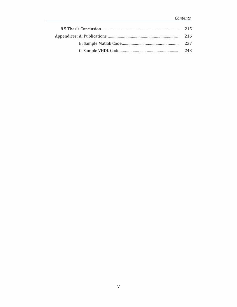
8.5 Thesis Conclusion…………………………………………………………….. 215
Appendices: A: Publications ………………………………………………………. 216
B: Sample Matlab Code……………….…………………………… 237
C: Sample VHDL Code………………….………………………….. 243

List of Figures
VI
List of Figures
2-1 The neuron…………………………………………………………………………...
13
2-2 Structure of the chemical synapse……………….................................... 13
2-3 The brain……………………………………………………………………………...
14
2-4 The Cerebral Cortex sections of the brain. The red area is the
Occipital lobe, yellow is the Parietal lobe, green is the
Temporal lobe and blue is the Frontal lobe [7]………………………..
15
2-5 The P300, a strong ERP component measured from the Fz
scalp site in a visual oddball stimulus. The stimulus onset is at
0 ms………………………………………………………………………………………
16
2-6 The classification of the EEG frequency bands………………………...
18
2-7 The international standard 10-20 system for EEG recording……
19
2-8 The EEG recording procedure with further processing towards
ERP extraction and signal analysis (e.g. CWT and WC)…….……..
20
2-9 The averaging over trials (Cz reference) showing the
improvement in the SNR as the number of trials increased. The
first waveform on the top row represents the EEG response to
the first stimulus. The following waveforms are the average of
an increasing number of trials (defined by n). The average of
30 trials is superimposed as a dot waveform……...............................
22
2-10 The generation of P300 ERP component as a result of stimulus
update…………………………………………………………………………………..
24
3-1 Two different forms for the same signal: (a) Discrete (b)
Digital…………………………………………………………………………………..
31
3-2 The butterfly: a basic computation unit in the FFT algorithm-
decimation in time…………………………………………………………………
37
3-3 The CWT scalogram of 1400 point EEG convolved with the
Morlet wavelet function…………………………………………………………
41
3-4 Complex Morlet wavelet function in the time domain (a1&a2)

List of Figures
VII
s=1, fc=1, real & imaginary Morlet (b1&b2) s=1, fc=0.318, real &
imaginary Morlet. (c) s=2, fc=1. (d) s=0.5, fc=1. ……………………….
43
3-5 Nassi-Shneiderman diagram for the digital implementation of
the FFT based CWT……………………………………………………………….
45
3-6 Sub-band decomposition of DWT…………………………………………... 46
3-7 Wavelet coherence example between two EEG signals……………
51
4-1 Different hardware platforms for the implementation of DSP
algorithms……………………………………………………………………………..
60
4-2 FPGA basic structure showing I/O, logic cells, multipliers,
block memory & interconnects………………………………………………
61
4-3 Generalized structure of a CLB slice.………………………………………
62
4-4 The design processing steps that precede the FPGA
programming………………………………………………………………………..
63
4-5 The CAD tool design circle ……………………………………………………
64
4-6 A design critical path and the latency delay…………………..............
68
4-7 The schematic block for the Xilinx FFT core V.5……………………..
70
4-8 Radix-2, burst I/O FFT core architecture...…………………………......
73
4-9 Radix-4, burst I/O FFT core architecture…..…………………………...
74
4-10 Pipelined, streaming I/O FFT architecture…..………………………....
75
4-11 Block diagram of the FFT core testing circuit…………………………
76
4-12 Schematic sheet section including the FFT core and the control
circuit for the core………………………………………….................................
77
4-13
The original sine wave and the reconstructed wave by the FFT
core……………………………………………………………………………………..
79
4-14
Figure 4-14: The produced quantization noise between the
sine waves in Fig. 4-13………………………………………………………….
79
4-15 The original EEG used in the FFT analysis and the EEG after
reconstruction……………………………………………………………………….
80
4-16 (a) Real FFT component for the EEG. (b) Imaginary component
80

List of Figures
VIII
4-17 The produced quantization noise from the imaginary data
output port following the IFFT process…………………………………..
81
5-1 (a) Clear EEG signal. (b) Contaminated EEG……………………...
89
5-2 (a) An EEG epoch of 2200 ms. (b) The single sided spectral
component of the EEG in (a)………………………………………………….
90
5-3 The reduction in noise versus averaging over trials………………...
92
5-4 Averaged EEG over 38 oddball epochs. (a1) Fz: 38 target
responses. (a2) Fz average. (b1) Cz: 38 target responses. (b2)
Cz average…………………………………………………………………………….
93
5-5 (a) The measured Fz channels during single oddball and
frequent trials. (b) and (c) The computed CWT coefficients for
oddball and for frequent trials. The colour bar was fixed on a
maximal value of 100 in both (b) and (c) for fair comparison.
The higher scales refer to lower frequencies………………………….
95
5-6 The wavelet cross spectrum (WCS) in oddball and frequent
trials (a1) Fz (red) and Cz (dashed-blue) signals in an oddball
trial. (a2) the wavelet cross spectrum (WCS) between Fz-Cz in
(a1). (b1) Fz (red) and Cz (dashed-blue) signals in a frequent
trial. (b2) The WCS between Fz-Cz in (b1) ………...…………………..
96
5-7 (Left contour) WC between Fz-Cz in an oddball trial. (Right
contour) WC between Fz-Cz in a frequent trial. The colour
scale refers to the magnitude of coherence in the time-
frequency plane…………………………………………………………………….
97
5-8 (a) The average WC image for the all oddball and frequent
trials for one of the participants and for the time window -200
to 1200 ms. The dashed vertical lines split the EEG frequency
bands. (b) The mean difference between WC according to EEG
frequency bands for one of the participants. Delta & theta
were merged into one band and gamma is considered in the
range (30-120 Hz). (c) The standardized normal form for the
average wavelet coherence difference between oddball and
frequent trials for all the 12 participants. ………………………………
98
5-9 (a) A matrix of selected oddballs (rows) with 6 subsequent
frequent trials (columns) after each oddball. The ‘O’ inside
the square refers to the oddballs whereas the letter ‘F’ refers
to the frequent trials following the oddball event. The arrow
refers to the increasing trial number from the oddballs. (b)
The wavelet coherence before and after threshold and the
chosen gamma window for analysis in the time duration
(350-600 ms) and frequency range (30-120 Hz). The

List of Figures
IX
selection of this window was based on a visual inspection of
the time series in Fig. 5-10…………………………………………………..
100
5-10 (a) The grand average of the oddball trials at Fz and Cz
electrodes for 12 participants (a total number of424 oddballs
were averaged). (b) The same averaging process for the
frequent trials (a total number of 2556 frequents were
averaged)……………………………………………………………………………..
101
5-11 The plots show the group averaged gamma coherence for
frequent trials at each of the trial positions after the last
oddball and for the time periods: (a) -200-0 ms, (b) 0-350 ms,
(c) 350-600 ms, (d) 600-900 ms. These groups of frequent
trials were depicted in Fig. 5-9 (a)………………………………………….
103
5-12 With 25000 iterations on the magnitude of correlation, the
Bootstrap method proves that the obtained high correlation in
Fig. 5-11 (c) is significant……………………………………………………….
104
5-13 The Z score bar for the difference between frequent and
oddball trials in the gamma section represented by wavelet
coherence as in Fig. 5-8 (c) except that the considered time
window is in the range 350-600 ms. The graph shows the
highest difference between the electrode pair Fz-Cz…....................
105
6-1 Flow chart for the digital implementation of the FFT based
CWT (based upon equation (3-23)). BRAM is used as a buffer;
SRAM ICs are used for final storage. A & B are the optimized
blocks in the design……………………………………………………………….
114
6-2 Morlet wavelet function in the frequency domain. (a) At scale
10. (b) At scale 20………………………………………………………………….
117
6-3 (a) Normalized wavelet function and an EEG signal in the
frequency domain. (b) The product of multiplication between
the signals in (a)…………………………………………………………………….
118
6-4 The Morlet wavelet function in the frequency domain with 37
different scales……………………………………………………………………..
121
6-5 The Morlet wavelet function in the frequency domain at 37
scales combined into one vector. The inset shows Morlet at
scale 10 before removing zeros……………………………………………..
122
6-6 The block diagram for the CWT engine…………………………………..
126
6-7 The schematic diagram for the CWT engine with the circle
areas magnified to show the CWT controller, multiplier
controller and the FFT core……………………………………………………
127

List of Figures
X
6-8 The timing simulation for the addresses generated by the
multiplier controller. (Upper) beginning of simulation. (Lower)
end of simulation…………………………………………………………………..
131
6-9 The product of multiplication between the EEG (real
component) and the Morlet wavelet function-scale 10
(frequency domain)………………………………………………………………
132
6-10 The multiplication and the truncation procedure…………………..
133
6-11 (a) An EEG signal showing an ERP from the visual stimulus
test. (b) The real and imaginary CWT components of the EEG
at scale 31. (c) The CWT magnitude-scale 31 (one scale band).
137
6-12 The CWT coefficients at scale 20 produced by both Matlab
software and FPGA………………………………………………………………...
137
6-13 The effect of overflow on the CWT coefficients (signified by a
dashed circle) -scale 31 based on FPGA………………………………...
140
6-14 The control circuit for the CWT coefficients in the BRAM……….
142
6-15 A design schematic sheet contains the CWT engine, data
transfer controller & the SRAM ICs with the circle areas
magnified to show these components…………………………………….
143
6-16 (a) The FPGA based CWT. (b) Software based CWT……………
145
6-17 The FFT of an EEG with the frequency range (a) 0.5-60 Hz. (b)
60-200 Hz……………………………………………………………………………..
146
6-18 The excluded Morlet scales (1-16) from the CWT
computations………………………………………………………………………..
146
6-19 The FPGA based CWT scalogram in the EEG frequency range
(1.95-62 Hz)………………………………………………………………………….
147
6-20 The CWT scalogram plots for an EEG signal (a) FPGA based
@133 MHz. (b) FPGA based @ 150 MHz distortion takes place.
(c) Software based…………………………………………………………………
149
7-1 Two measured EEG waveforms during the Oddball test from
the brain sites Fz & Cz. (b) the CWT for Fz. (c) the CWT for Cz.
159
7-2 The flow diagram for the wavelet coherence algorithm
(equation 7-1)…………………………………………………………...…………..
160
7-3 Simplified flow diagram for the WC algorithm………………………. 161

List of Figures
XI
7-4 Wavelet coherence between the EEGs in Fig. 7-1(a)-software
based…………………………………………………………………………………….
163
7-5 (a1, a2 & a3) Software based CWT1, its real & imaginary
components respectively. (b1, b2&b3) FPGA based CWT1, its
real & imaginary components respectively. The white circle
shows the region where the effect of overflow appears…………
164
7-6 WCS (a) Real component. (b) Imaginary component. (c)
Magnitude……………………………………………………………………………..
165
7-7 Wavelet coherence between the hardware based CWT1 &
CWT2. The effects of overflow are noticeable when compared
against Fig. 7-4………………………………………………………………………
166
7-8 Wavelet coherence with elimination to the existent overflow in
Fig. 7-7. ……………………………………………………...…………………………
167
7-9 The effect of frequency smoothing on a wavelet auto-spectrum
(a) Before smoothing. (b) After smoothing……………………………
169
7-10 Wavelet coherence in different word lengths: (a) the target
WC- software based. (b1), (b2), (b3): 16-bit word length with
2, 8 and 16 colours respectively. (c1), (c2), (c3): 32-bit word
length with 2, 8 and 16 colours respectively…………………………..
175
7-11 Wavelet coherence: mistaken features start to appear when
the number of graded colours increased to 64 (compared to
Fig. 7-10 a)………………………………………...................................................
176
7-12 The CWT design and the WC design in the FPGA with the SRAM
ICs used for storing results…………………………………………………….
179
7-13 The storage locations of CWT1 & CWT2 in the SRAM ICs………..
180
7-14 The proposed schematic diagram to calculate the WCS and the
auto-spectrums in VHDL. The bus number refers to its word-
length……………………………...........................................................................
182
7-15 The locations of CWT1 (real) in the wavelet plane indicating
the coefficients that smoothed together. The black, blue and
yellow circles represent the smoothed coefficients at time
index t1, t2 and t 1024 respectively……………………………………….
184
7-16 The timing simulation for the address switching method of
SRAM0 to implement the smoothing function…………………………
186
7-17 The proposed schematic for the 32-bit smoothing circuit. The
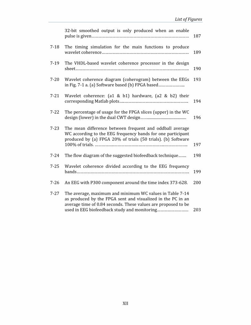
List of Figures
XII
32-bit smoothed output is only produced when an enable
pulse is given…………………………………………………………………………
187
7-18 The timing simulation for the main functions to produce
wavelet coherence…………………………………………………………………
189
7-19 The VHDL-based wavelet coherence processor in the design
sheet…………………………………………………………………………….……….
190
7-20 Wavelet coherence diagram (coherogram) between the EEGs
in Fig. 7-1 a. (a) Software based (b) FPGA based…………………..
193
7-21 Wavelet coherence: (a1 & b1) hardware, (a2 & b2) their
corresponding Matlab plots…..……………………………………………….
194
7-22 The percentage of usage for the FPGA slices (upper) in the WC
design (lower) in the dual CWT design…….........................................
196
7-23 The mean difference between frequent and oddball average
WC according to the EEG frequency bands for one participant
produced by (a) FPGA 20% of trials (50 trials). (b) Software
100% of trials. ……………..……………………………………..………………..
197
7-24
The flow diagram of the suggested biofeedback technique……. 198
7-25 Wavelet coherence divided according to the EEG frequency
bands…………………………………………………………………………………….
199
7-26 An EEG with P300 component around the time index 373-628. 200
7-27 The average, maximum and minimum WC values in Table 7-14
as produced by the FPGA sent and visualized in the PC in an
average time of 0.84 seconds. These values are proposed to be
used in EEG biofeedback study and monitoring………………………
203

List of Tables
XIII
List of Tables
3-1 Example of coherence measure between two -14 element
vectors (x & y) in 4 different cases where x becomes closer to
y for case 1 towards 4. The coherence result can be seen in
the last row………………………………………………………………………...
50
4-1 FFT core pin-out…...…………………………………………………………… 72
4-2 Three outputs for the FFT core status………………………………… 78
6-1 Three different wavelet bases in two domains……………………. 115
6-2 The used scales in the CWT design with the corresponding
frequencies………………………………………………………………………..
120
6-3 Nonzero Morlet points and the corresponding EEG
points………………………………………………………………………..............
123
6-4 FPGA synthesis results summary ………………………………………. 135
6-5 The total number of clock cycles divided by the task…………... 135
6-6 The correlation coefficients between software and hardware
CWT at scales 5, 10, 15 & 17-37…………………………………………
138
6-7 Timing schedule for the BRAM & SRAM IC with the FFT core
(clock cycles number between brackets)…………………………….
141
6-8 Comparison of timing schedule for the design in two
different ranges of wavelet scale ……………………………………….
148
6-9 The locations of the CWT coefficients in SRAM0 & SRAM1
ICs……………………………………………………………………………………
150
6-10 The FPGA synthesis report of the design in two EEG signals
to be analysed with the included Morlet wavelet scales………
150
6-11 The degree of closeness between the software and hardware
CWT coefficients in three normalized methods - scale based.
The software scalogram is the reference……………………………
151
6-12 The degree of closeness between the software and hardware
CWT scalogram plots in three normalized methods. The
software scalogram is the reference………………………………….
152
6-13 Comparison of VLSI based CWT implementations from the
List of Tables
XIV
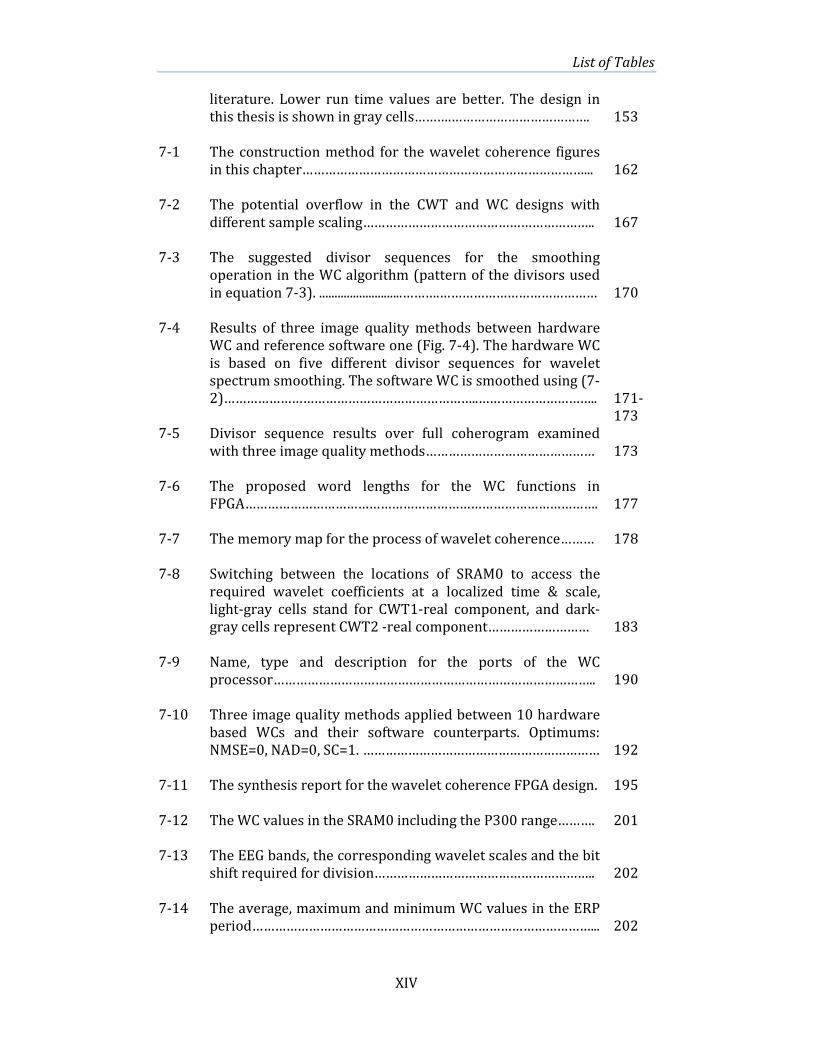
literature. Lower run time values are better. The design in
this thesis is shown in gray cells……….……………………………….
153
7-1 The construction method for the wavelet coherence figures
in this chapter…………………………………………………………………...
162
7-2 The potential overflow in the CWT and WC designs with
different sample scaling……………………………………………………..
167
7-3 The suggested divisor sequences for the smoothing
operation in the WC algorithm (pattern of the divisors used
in equation 7-3). ...........................……….……………………………………
170
7-4 Results of three image quality methods between hardware
WC and reference software one (Fig. 7-4). The hardware WC
is based on five different divisor sequences for wavelet
spectrum smoothing. The software WC is smoothed using (7-
2)…………………………………………………………..…………………………..
171-
173
7-5 Divisor sequence results over full coherogram examined
with three image quality methods………………………………………
173
7-6 The proposed word lengths for the WC functions in
FPGA………………………………………………………………………………….
177
7-7 The memory map for the process of wavelet coherence……… 178
7-8 Switching between the locations of SRAM0 to access the
required wavelet coefficients at a localized time & scale,
light-gray cells stand for CWT1-real component, and dark-
gray cells represent CWT2 -real component………………………
183
7-9 Name, type and description for the ports of the WC
processor…………………………………………………………………………..
190
7-10 Three image quality methods applied between 10 hardware
based WCs and their software counterparts. Optimums:
NMSE=0, NAD=0, SC=1. ………………………………………………………
192
7-11 The synthesis report for the wavelet coherence FPGA design. 195
7-12 The WC values in the SRAM0 including the P300 range………. 201
7-13 The EEG bands, the corresponding wavelet scales and the bit
shift required for division…………………………………………………..
202
7-14 The average, maximum and minimum WC values in the ERP
period………………………………………………………………………………...
202
Glossary of Abbreviations and Terms
XIX
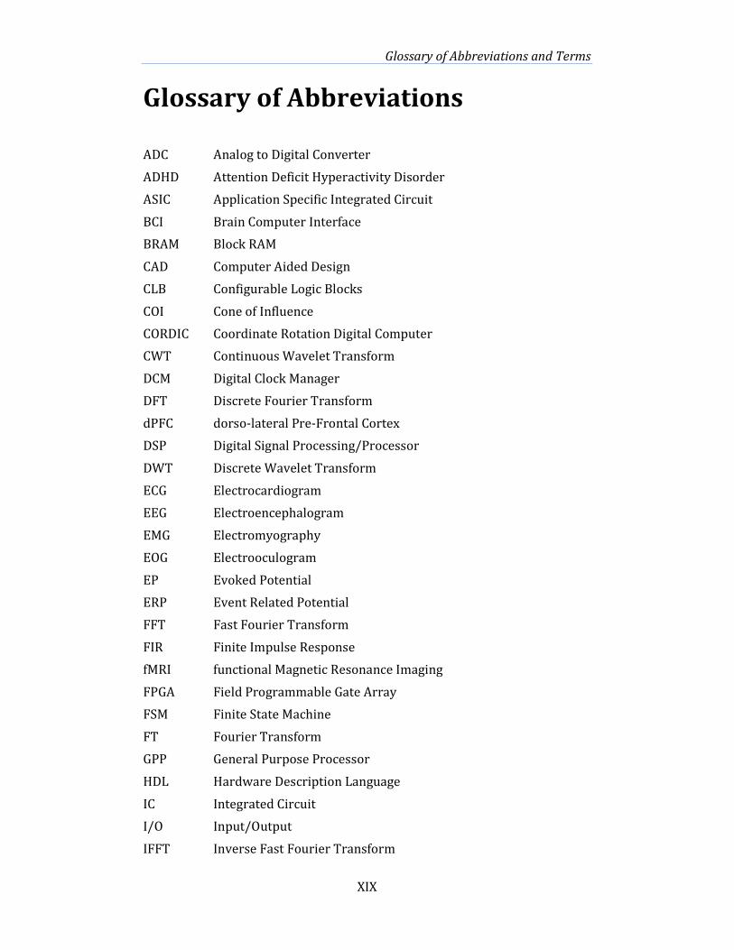
Glossary of Abbreviations
ADC Analog to Digital Converter
ADHD Attention Deficit Hyperactivity Disorder
ASIC Application Specific Integrated Circuit
BCI Brain Computer Interface
BRAM Block RAM
CAD Computer Aided Design
CLB Configurable Logic Blocks
COI Cone of Influence
CORDIC Coordinate Rotation Digital Computer
CWT Continuous Wavelet Transform
DCM Digital Clock Manager
DFT Discrete Fourier Transform
dPFC dorso-lateral Pre-Frontal Cortex
DSP Digital Signal Processing/Processor
DWT Discrete Wavelet Transform
ECG Electrocardiogram
EEG Electroencephalogram
EMG Electromyography
EOG Electrooculogram
EP Evoked Potential
ERP Event Related Potential
FFT Fast Fourier Transform
FIR Finite Impulse Response
fMRI functional Magnetic Resonance Imaging
FPGA Field Programmable Gate Array
FSM Finite State Machine
FT Fourier Transform
GPP General Purpose Processor
HDL Hardware Description Language
IC Integrated Circuit
I/O Input/Output
IFFT Inverse Fast Fourier Transform
Glossary of Abbreviations and Terms
XX
IP Intellectual Property
ISE Integrated Software Environment
JPEG Joint Photographic Experts Group
JTAG Joint Test Advisory Group
LUT Look-Up Table
MAC Multiply and Accumulate
MEG Magneto-Encephalography
MFG Middle Frontal Gyrus
MSC Magnitude Squared Coherence
NAD Normalized Average Difference
NFFT Number of Fast Fourier Transform points
NGC Xilinx Generated Netlist File
NMSE Normalized Mean Square Error
OFDM Orthogonal Frequency Division Multiplexing
PC Personal Computer
PET Positron Emission Tomography
PCB Printed Circuit Board
PSD Power Spectral Density
RMS Root Mean Square
SC Structural Content
SD Standard Deviation
SNR Signal-to-Noise Ratio
SPSS Significance of the Pearson Correlation Coefficients
SRAM Static Random Access Memory
STFT Short Time Fourier Transform
UART Universal Asynchronous Receiver/Transmitter
USB Universal Serial Bus
VEP Visual Evoked Potential
VHDL Very High Speed Integrated Circuit Hardware Description Language
VR Visual Reality
WC Wavelet Coherence
WCS Wavelet Cross Spectrum
WT Wavelet Transform

Glossary of Abbreviations and Terms
XXI
Glossary of Terms
Amygdala……………………….... Groups of nuclei within the brain for emotional
reactions and memory processing.
Axon………………………………… Long nerve fibre in the neuron.
Biofeedback……………………… The electrophysiological state of participants
to be observed in a short delay and an action to
that observation to be taken.
Bootstrap…………………………. A statistical method to sample estimates used
for specifying the accuracy of undertaken
measures.
Cerebral cortex………………… Surface layer of the cerebrum of the brain.
Cerebrum………………………… The main part of the brain responsible for
controlling the central nervous system of the
brain.
Coherogram……………………. Time-frequency plane of wavelet coherence
Cone of influence……………… The continuous wavelet transform at the
boundaries of the transformed signal.
Configurable logic blocks..... Programmable cells inside the FPGA; can be
configured to different logic.
Critical path……………………. Maximum delay between two storage elements
in a digital design.
Dendrites…………………………. Branched outcrop of the neuron.
Dynamic configuration…….. An FPGA technique which allows for device
reconfiguration during the operation mode.
Dynamic range………………… Representation of numbers in the given range
where no overflow or underflow exists.
Endogenous……………………. Related to the ERP waveform based on higher-
order processing of a stimulus.
Exogenous………………………. Related to the ERP waveforms based on
features of a stimulus.
Forebrain……………………….. One of three major parts of the brain. See Fig.
2-3.
Gland cell………………………… Sheet of cells that lines the body cavity or
covers the surface of a body.
Hindbrain………………………. See Fig. 2-3

Glossary of Abbreviations and Terms
XXII
Hippocampus………………….. A major component of the brain that plays a
vital role in spatial navigation and integration
of information from short-term memory to
long-term memory.
Hypothalamus………………… Brain section with a variety of functions.
Inion……………………………….. The most prominent projecting point of the
occipital bone located at the base of the skull.
Midbrain…………………………. See Fig. 2-3
Motor potential………………… Measure of activity in the cerebral cortex that
leads to voluntary movement of muscle.
Myelin sheath………………….. A dielectric material covering the axon of a
neuron.
Nasion…………………………….. The middle point of the nasofrontal suture.
Node of Ranvier………………. Gaps located within the myelin sheaths of the
neuron.
Non-stationary
signal…………
Signals with different frequency components
at each time.
Occipital………………………….. The bone at the back of the skull.
Offline processing…................ Non-real time processing.
Parietal…………………………… Brain part above the occipital lobe and behind
the frontal lobe. See Fig. 2-4.
Preauricular points………….. Related to the ear.
Reaction time…………………… The duration between the stimulus onset and
participant response.
Scalogram………………………… Time-frequency plane of the continuous
wavelet transform with colours that refer to
different power regions.
Smoothing……………………….. Averaging over coefficients towards time or
frequency.
Soma……………………………….. Cellular body of the neuron.
Somatosensory………………… Diverse sensory system of the body.
Standardized normal form... Normal distribution with a standard deviation
of 1 and a mean of 0.
Synapse…………………………… Contact points between neurons
Temporal lobe…………………. See Fig. 2-4.
Thalamus…………………………. A symmetrical portion within the brain.
Timing simulation……………. A waveform diagram that verifies the
operation of a digital design.
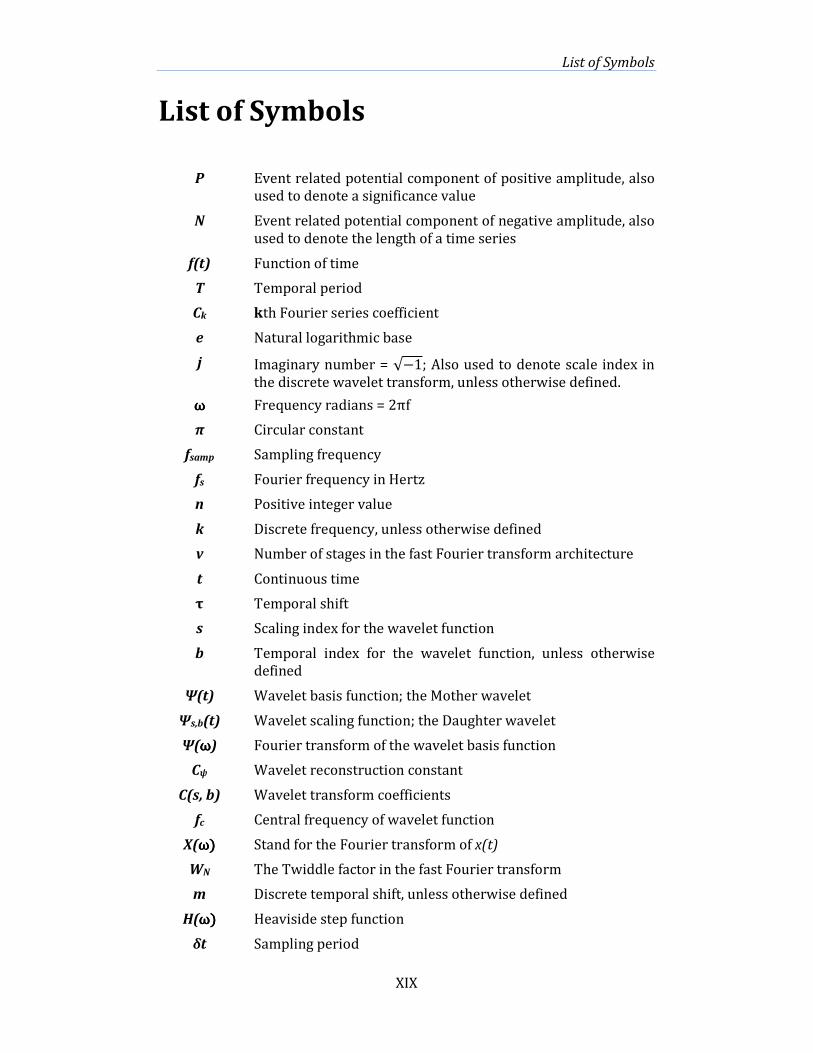
List of Symbols
XIX
List of Symbols
P Event related potential component of positive amplitude, also
used to denote a significance value
N Event related potential component of negative amplitude, also
used to denote the length of a time series
f(t) Function of time
T Temporal period
Ck kth Fourier series coefficient
e Natural logarithmic base
j Imaginary number = √−1; Also used to denote scale index in
the discrete wavelet transform, unless otherwise defined. ⍵⍵⍵⍵ Frequency radians = 2πf
π Circular constant
fsamp Sampling frequency
fs Fourier frequency in Hertz
n Positive integer value
k Discrete frequency, unless otherwise defined
v Number of stages in the fast Fourier transform architecture
t Continuous time
τ Temporal shift
s Scaling index for the wavelet function
b Temporal index for the wavelet function, unless otherwise
defined
Ψ(t) Wavelet basis function; the Mother wavelet
Ψs,b(t) Wavelet scaling function; the Daughter wavelet
Ψ(⍵⍵⍵⍵) Fourier transform of the wavelet basis function
Cψ Wavelet reconstruction constant
C(s, b) Wavelet transform coefficients
fc Central frequency of wavelet function
X(⍵⍵⍵⍵)))) Stand for the Fourier transform of x(t)
WN The Twiddle factor in the fast Fourier transform
m Discrete temporal shift, unless otherwise defined
H(⍵⍵⍵⍵)))) Heaviside step function
δt Sampling period

List of Symbols
XX
ha Low pass filter coefficient of the discrete wavelet transform
ga High pass filter coefficient of the discrete wavelet transform
cj(n) Approximation coefficient
dj(n) Details coefficients
ρ2(f) Fourier magnitude coherence
Sxx Fourier transform of the autocorrelation function x
Sxy(f) Cross-spectral density of the functions x & y
Rxy(τ) Cross-correlation function of the functions x & y
S Smoothing operator
s-1 Energy density factor ��� Wavelet cross spectrum of the functions x & y ��� Wavelet auto-spectrum of function x �� Square wavelet coherence (magnitude)
Fz Denotes a brain frontal site
Cz Denotes a brain central site
Φxy(f) Wavelet coherence (phase) �(�, �) Original image coefficient ��(�, �) Reconstructed image coefficient
yaverage Signal averaging over a number of epochs
yr Sum of r time series ����� Representative quantity of noise following signal averaging
Z Standardized normal form
Nr Base-to-peak voltage measure of noise ��� Average voltage of noise ���� Gamma function
Th Decision threshold
R2 Correlation value
J1 Wavelet scale number minus one
DJ Space between discrete scales
S0 Wavelet smallest scale
MEM Denotes a memory block
< > Smoothing in time or frequency
Chapter One
1
Chapter 1
Introduction This thesis examines the FPGA design and implementation of the
continuous wavelet transform (CWT) and wavelet coherence (WC) for EEG
signals. In addition, it provides the means for a possible biofeedback
mechanism based on the WC.
This first chapter will provide an extended overview of the scientific
and engineering questions investigated in this thesis. It will also serve as a
“road map” to the sections that expand upon and provide details concerning
the key concepts examined.
Electroencephalogram (EEG) waveforms provide an important source
of information for the study of human cognition states [1]. The measurement
of these electrical activities can be taken from standardized channel locations
on the scalp [2]. Generally, the selection of the appropriate brain channels for
analysis depends on the cognitive processes being studied and the questions
being addressed [3]. In most of the cases extracting useful information from
the EEG requires a conversion process on these signals to another useful
form. One of these powerful transformation tools in the field of EEG is the
wavelet transform (WT). The continuous wavelet transform provides
necessary information on the non-stationary EEG signals in the time-
frequency plane, and the wavelet coherence shows the correlation between a
pair of EEG channels in the wavelet domain [4]. The effectiveness of this WC
analysis in studying the neural networks of the brain in multiple behaviours
has been previously shown [5]. It has been reported in the literature that WC

Chapter One
2
can be applied to assess cognitive processes and provides the phase
parameters that can be fed back to participants related to their generated
electrical activities [6]. Such biofeedback may, for example, involve
presenting a visual stimulus to the participant during the EEG recording
session. This stimulates the EEG to produce the event related potential (ERP)
components, for example the P300 (a positive potential arising 300-600 ms
post stimulus [1]). The extracted biofeedback parameters from the EEG can
provide the participant with information regarding his cognitive
performance accurately and quickly. For example, it could provide feedback
for updating the participant’s attention state [7]. In the case of analysing the
EEG with the wavelet coherence technique, the amount of data and
computation becomes extensive and the visual-interpretation of this data is
difficult [8]. Early investigations undertaken in this thesis aimed to reduce
the amount of data by determining and specifying the most suitable brain
channels as a source of data and including the analysed WC data in a
comprehensive scheme for interpretation.
The wavelet transform has been widely used in the field of EEG
analysis, although high-speed wavelet processing of EEGs may still be a
challenge with a montage of 64 or 128 electrodes being common. Recent
studies have shown increased trends towards real time EEG applications
such as the brain computer interface [9], neurofeedback and studies of
attention and learning [10]. Processing of the EEG signals can be undertaken
either after collecting and saving the data (which is known as off-line
processing) or instantly during the measurement process (which is known as
on-line or real-time processing). Off-line processing of data can be applied in
many useful applications by analysing the previously recorded EEG, for
example diagnosing brain abnormalities [11]. In such a case, high speed
processing is not urgent and has no effect on the analysed data. On the other
hand, on-line processing requires producing the results of analysis to
participants with a minimum delay following the data measurement
procedure. This enables the participants to observe their electrophysiological

Chapter One
3
state and allows for feedback control [10]. When the EEG data is processed
slowly, the feedback signal may not appear at the required time and the
whole application becomes unsuccessful. One factor that negatively affects
the period of delay time for biofeedback is the complexity of the algorithm
applied to analyse the EEG. It is well known that hardware processing is
faster than software, and can be a viable alternative to the software for
biofeedback computations. In general, when the measured EEG is not a part
of the presented stimulus to a participant, on-line processing of the EEG is
not required and the included operations in the applied algorithm can be off-
line processed [12]-[13].
For real-time EEG signal analysis with the CWT, it will be argued that
software processing is not sufficient and hardware processing needs to be
involved. Furthermore, WC contains more operations than the CWT since
two CWT scalograms are required to construct one WC (see section 5.3.3.1),
followed by additional complex operations. As a result, WC needs more
computations than the CWT, and the involvement of hardware computations
in real-time applications is crucial. The CWT hardware design needs to be
fast enough to process the ERP in a few milliseconds and to permit a
reasonable time for the feedback. Hardware processing is fast and can
provide portability due to its small size. However, it may produce less
accurate results than the software processing because of the appearance of
quantization errors. The hardware is limited to a resolution based upon the
platform used but the software is not so limited, hence a reduction in the
quantization noise. The quantization error depends on the size of the word
length bit selection used in the binary number representation of data [14].
For a reasonable precision to the EEG signals, sufficient word length needs to
be selected due to the complexity of the signal. Word length selection has an
impact on the required resources for design and power consumption [15].
One of the hardware technologies that has been extensively used in
the last two decades for real time signal processing is the field programmable
gate array (FPGA). The FPGA (see section 4.1.1) is a high-speed integrated

Chapter One
4
circuit with a wide range of hardware resources. It can be re-programmed
and reconfigured according to the architecture of the design. In addition,
there is a noticeable trade-off between performance and flexibility.
Furthermore, the FPGA system is small, inexpensive and portable [16]. The
FPGA was employed in the analysis of EEGs in this thesis to perform the
required computations in a few milliseconds and to provide the means for
high speed CWT analysis and EEG biofeedback. By using advancements in
VLSI systems, building low cost, lightweight, portable and non-invasive
systems for real time EEG processing and biofeedback can be achieved.
1.1 Research Topic
Previous studies of coherence have shown the value of the technique
in finding connectivity and binding between cortical areas within the
frequency bands of the EEG and results to enhance cognitive control [5], [7].
As the WC requires two CWT scalogram planes to be constructed, some
studies have shown off-line processing on the previously recorded EEG [11],
[17]. Despite previous research on individual ERP signals using FPGA [9], the
involvement of CWT and WC techniques to analyse EEG signals in a high
speed FPGA design has not become a research field of interest. This lack of
research investigating the CWT and WC in the processing of EEGs and ERP
was the motivation to these investigations in this work. The EEGs used in the
analysis were recorded from healthy participants through a visual test and
used for a pilot study in this thesis and later for examining both the CWT and
the WC processors.
The first phase of this thesis aimed to show the utility of WC analysis
for identifying more clearly individual trial features that are not easily
detected in the raw time series. In addition, the WC was used to investigate
possible evidence for the brief activation of fronto-central/parietal brain
areas. Moreover, averaging in the wavelet domain was applied to test for
coherence between electrode sites that relate to the cognition processes
involved in monitoring the visual stimulus event. For the two types of visual
stimuli, the “oddball” and the “frequent”, the EEG was measured and the WC

Chapter One
5
was calculated. In addition, the expectancy hypothesis was examined by the
post-oddball trial position of a series of frequent trials in the means of WC.
These investigations were presented in chapter 5 of this thesis.
The second phase of work for the thesis aimed at designing and
implementing a novel high-speed FPGA architecture to process the EEG
signals utilizing the CWT technique. The calculations were performed in the
frequency domain to reduce complexity since the convolutions become
multiplications in this domain. Computer Aided Design (CAD) tools were
used for design entry, synthesis, timing simulation and final implementation.
The CWT design was tested by typical EEG waveforms from the participant
group and verified with the same analysis, undertaken by software using
image quality algorithms. These applied algorithms showed a high level of
accuracy in the hardware results. Optimization was openly undertaken to
reduce the silicon area in order to fit the entire components of the CWT
design into a low cost FPGA platform. In addition, space can be saved and the
design expanded if the two EEG waveforms are analysed sequentially. These
optimizations also showed a reduction in the number of computations and an
increase in operational speed.
In the third phase of this thesis, the whole system was developed to
produce the WC from two CWT scalograms. A criterion for using this WC in a
biofeedback test was proposed. Chapters 6 and 7 will describe the entire
architecture of the design with consideration given to most of the required
hardware design aspects. The high processing speed obtained can lead to the
use of the hardware wavelet engine in real-time EEG applications.
1.2 Thesis Outline
Chapter 2 summarises EEG topics starting from the neuroelectric
waveform generation, brain physiology and related functions. A brief
overview of the main parts of the brain and the neuron is outlined as
background for the reader. The connectivity of brain channels and the theory
of electrode placement systems are also provided, in addition to the EEG
Chapter One
6
characteristics. A brief overview of the evoked potential (EP) and the event
related potential (ERP) components is given with special attention to the
P300. The recording of neuroelectric waveforms is covered with some
discussion on artefact noise.
Chapter 3 outlines the standard signal processing techniques for the
analysis of the time series epochs including the most popular Fourier
transform (FT), fast Fourier transform (FFT), the wavelet transform and its
effective applications to the non-stationary EEG and ERP signals. This chapter
also presents details on the wavelet function used in this thesis and the
concepts needed to understand the WC. Finally, some techniques used later
in this thesis to qualify scalogram images are also presented.
Chapter 4 explains the hardware design aspects for EEG processing
using the wavelet technique, in addition to the FPGA structure and hardware
description language (HDL) design flow. Word length (bit width) selection,
design size, timing constraints and design optimization are discussed. This is
followed by a description and testing of the Xilinx fast Fourier transform
(FFT) core for the FFT-IFFT processes.
Chapter 5 presents the development of the novel wavelet coherence
based method of characterising and analysing brain electrical activity under
the visual oddball test. The wavelet coherence was averaged along the EEG
bands and the correlation in the gamma band was tested. Descriptions,
interpretation and support for the wavelet coherence results, with
justification to the selected brain channels for EEG measurements, are also
presented. An assessment of the obtained WC results is explained in the
discussion section of this chapter.
Chapter 6 presents the design and implementation of the continuous
wavelet transform engine for non-stationary signals on FPGA and the
optimization methods for such a complex architecture. The high-speed
integrated circuit Hardware Description Language (VHDL) controllers
(designed for calculating the CWT coefficients) are presented in detail and
Chapter One
7
the performance of the design is assessed. The CWT design is specified for
analysing signals in the EEG frequency range as an optimization and
development to the design. The optimization procedure in the design assisted
in saving further FPGA resources. These resources were used to develop
another CWT for a second EEG signal. With the availability of two CWT
scalogram plots, wavelet coherence can be produced.
Chapter 7 outlines the details of the wavelet coherence design in
hardware. This design relies upon the produced results from the CWT design
in Chapter 6. Wavelet coherence was tested by software regarding the
smoothing process and word length limitations as pre-steps towards the
presented FPGA implementation in Chapter 7. This chapter also
demonstrates a method that speeds up the transfer of WC information from
the FPGA to the personal computer (PC), which enables the WC design to be
used for monitoring and biofeedback studies. The transferred coefficients are
compared with the same one calculated by software.
Finally, Chapter 8 presents a review of the work, summary and
conclusion from the obtained results. It also discusses the potential for
further work that may improve the methods and design presented.
1.3 Publications
The completed work in this thesis on EEG analysis using wavelet
transform and wavelet coherence, the design of the wavelet power spectra
and coherence detection engines has produced three journal articles (one
published and two under review), two conference publications and one
accepted abstract for conference presentation.
Conferences:
(Peer reviewed)
• Yahya T. Qassim, Tim R. H. Cutmore, David D. Rowlands,
“Multiplier Truncation in FPGA Based CWT”, Proceedings of
Chapter One
8
the International Symposium on Communications and
Information Technologies (ISCIT), 2012, pp. 952-956.
• Yahya T. Qassim, Tim R. H. Cutmore, David D. Rowlands, “FPGA
Implementation of Morlet Continuous Wavelet Transform
for EEG Analysis”, Proceedings of the International Conference
on Computer and Communication Engineering (ICCCE), 2012,
pp. 59-64.
(Abstract presented)
• Yahya T. Qassim, Tim R.H. Cutmore, David D. Rowlands, “High
Performance Specific CWT Architecture for EEG Analysis”,
16th Biennial Computational Techniques and Applications
Conference (CTAC 2012), Sept. 23-26, 2012.
Journal articles:
(Published)
• Yahya T. Qassim, Tim R. H. Cutmore, Daniel A. James, David D.
Rowlands, “Wavelet Coherence of EEG Signals for A Visual
Oddball Task”, Computers In Biology and Medicine (CIBM), vol.
43, pp. 23-31, Jan. 1, 2013.
(Under review)
• Yahya T. Qassim, Tim R. H. Cutmore, David D. Rowlands,
“Optimized FPGA Based Continuous Wavelet Transform”,
Computers and Electrical Engineering.
• Yahya T. Qassim, Tim R. H. Cutmore, David D. Rowlands, “FPGA
Implementation of Wavelet Coherence for EEG and ERP
Signals”.
Chapter One
9
1.4 References
1 E. Niedermeyer and F. L. D. Silva, “Electroencephalography: Basic
Principles, Clinical Applications, and Related Fields,” Fifth ed. Philadelphia: by Lippincott Williams & Wilkins, 2005.
2 A. Mouraux and G. Iannetti, "Across-trial averaging of event-related EEG
responses and beyond," Magnetic resonance imaging, vol. 26, pp. 1041-
1054, 2008.
3 M. Teplan, "Fundamentals of EEG measurement," Measurement Science
Review, vol. 2, 2002.
4 J.-P. Lachaux, A. Lutz, D. Rudrauf, D. Cosmelli, M. L. V. Quyen, J. Martinerie,
and F. Varela, "Estimating the time-course of coherence between single-
trial brain signals: an introduction to wavelet coherence," Neurophysiol
Clin, vol. 32, pp. 157-174, 2002.
5 R. N. Romcy-Pereira, D. B. de Araujo, J. P. Leite, and N. Garcia-Cairasco, "A
semi-automated algorithm for studying neuronal oscillatory patterns: a wavelet-based time frequency and coherence analysis," Journal of
neuroscience methods, vol. 167, pp. 384-392, 2008.
6 D. Varoqui, J. Froger, J. Y. Pélissier, and B. G. Bardy, "Effect of coordination
biofeedback on (re) learning preferred postural patterns in post-stroke
patients," Motor Control, vol. 15, pp. 187-205, 2011.
7 A. W. Keizer, R. S. Verment, and B. Hommel, "Enhancing cognitive control
through neurofeedback: A role of gamma-band activity in managing
episodic retrieval," Neuroimage, vol. 49, pp. 3404-3413, 2010.
8 A. Klein, T. Sauer, A. Jedynak, and W. Skrandies, "Conventional and wavelet
coherence applied to sensory-evoked electrical brain activity,"
Biomedical Engineering, IEEE Transactions on, vol. 53, pp. 266-272, 2006.
9 S. Kuo-Kai, L. Po-Lei, L. Ming-Huan, L. Ming-Hong, L. Ren-Jie, and C. Yun-Jen, "Development of a Low-Cost FPGA-Based SSVEP BCI Multimedia Control
System," Biomedical Circuits and Systems, IEEE Transactions on, vol. 4, pp. 125-132, 2010.
10 P. L. Purdon, H. Millan, P. L. Fuller, and G. Bonmassar, "An open-source
hardware and software system for acquisition and real-time processing
of electrophysiology during high field MRI," Journal of neuroscience
methods, vol. 175, pp. 165-186, 2008.

Chapter One
10
11 V. Sakkalis, T. Oikonomou, E. Pachou, I. Tollis, S. Micheloyannis, and M.
Zervakis, "Time-significant wavelet coherence for the evaluation of schizophrenic brain activity using a graph theory approach," in
Engineering in Medicine and Biology Society, 2006. EMBS'06. 28th Annual
International Conference of the IEEE, 2006, pp. 4265-4268.
12 C. D'Avanzo, V. Tarantino, P. Bisiacchi, and G. Sparacino, "A wavelet
methodology for EEG time-frequency analysis in a time discrimination
task," International Journal of Bioelectromagnetism, vol. 11, pp. 185-188,
2009.
13 C. N. Gupta, Y. U. Khan, R. Palaniappan, and F. Sepulveda, "Wavelet
framework for improved target detection in oddball paradigms using
P300 and Gamma band analysis," Biomedical soft computing and human
sciences, vol. 14, pp. 61-67, 2009.
14 D. Oh and K. K. Parhi, "Min-sum decoder architectures with reduced word length for LDPC codes," Circuits and Systems I: Regular Papers, IEEE
Transactions on, vol. 57, pp. 105-115, 2010.
15 J. E. Stine and O. M. Duverne, “Variations on truncated multiplications,” Proceedings of the Euromicro Symposium on Digital System Design (DSD’03),
2003, pp. 112-119.
16 W. Zhang, V. Betz, and J. Rose, "Portable and scalable FPGA-based
acceleration of a direct linear system solver," ACM Transactions on
Reconfigurable Technology and Systems (TRETS), vol. 5, p. 6, 2012.
17 Y. Qi, V. Siemionow, Y. Wanxiang, V. Sahgal, and G. H. Yue, "Single-Trial EEG-
EMG Coherence Analysis Reveals Muscle Fatigue-Related Progressive Alterations in Corticomuscular Coupling," Neural Systems and
Rehabilitation Engineering, IEEE Transactions on, vol. 18, pp. 97-106, 2010.
Chapter Two
11
Chapter 2
The Cognitive System and
Electroencephalography
Electroencephalogram (EEG) waves have been a field of study and
investigation for more than 100 years. Human EEG activity was first recorded
and depicted in 1924 by Hans Berger when he noticed changes in this activity
accompanying the functional status of the participant’s brain [1]. Thereafter,
the utility of EEG patterns and complications have progressed enormously
due to their importance in providing temporal information within the brain,
giving an understanding of the functionality of cognitive processes.
The EEG is an incommodious and inexpensive tool to be used in the
brain field. EEG digitization has allowed constant storage of data to be saved
for offline analysis and development. Recent research trends focus on the
real time applications of the EEG in which individual epochs1 are sufficient
for analysis [2]. These applications are closed loop systems that enable the
user to send intensions to the external world without utilization of muscles
[3]. These intensions can be involved in various applications. The visual
evoked potential (VEP) activities that are produced by the brain represent
essential components for the operation of these applications. For example,
brain computer interface (BCI) and virtual reality (VR) control have been
widely used for entertainment and gaming purposes and they strongly
depend on the motivation and engagement of the user, which helps for better
generation of his VEP [4].
1 A chop of continuous EEG data is called an ‘epoch’.
Chapter Two
12
In clinical practice, EEG is widely used due to the significant
information that can be obtained from the recorded data within a millisecond
resolution. It is extensively applied to assess a patient’s consciousness or
change in arousal level such as sleep. In addition, EEG is used to investigate a
dysfunction in a certain brain section that could be associated with a specific
problem for a patient. Furthermore, it is considered a powerful tool in both
neurology and clinical neurophysiology fields due to its ability to reflect the
state of the electrical activity of the brain in its rhythms energy and
connectivity across different brain regions [5]-[6].
This chapter outlines the basic concepts of brain physiology, the EEG
waves and the cognitive system to understand the brain anatomy and the
generation of its electrical activity. In addition, a brief review of the
functional connectivity of the brain is also presented. These preliminaries are
required before performing any analysis on the EEG.
2.1 Neuroelectric Waveform
2.1.1 Generation and Signal Transmission
To understand the electrical activity of the brain, a short description of
its basic unit ‘the neuron’ is outlined. This specialized cell is designed to
transmit or receive information to and from other nerves, gland cells or
muscle. It represents the basic functioning unit of the brain. The number of
structured neurons in the brain range between 1 billion and 100 billion [1].
The neuron consists of the cellular soma (body) that contains the nucleus of
the nerve cell, the axon and dendrites. The axonal membrane is efficiently
insulated by a wrapping of myelin sheath except at the nodes of Ranvier
where the axon is able to generate an electrical activity [7], as illustrated in
Fig. 2-1.
Each neuron makes contact with other cells through contact points
called synapses. The soma and the dendrites are covered with synapses
connecting with the ends of axons from other neurons [8]. Fig. 2-2 shows the
structure of a typical synapse. A transmitted form of pulses inside the axon
fibres represents the signals [9]. Synaptic transmission is chemical and
behaves as a valve. As a response to the neural impulse, the vesicles on the
Chapter Two
13
presynaptic membrane release neurotransmitters (transmitter substances)
that are distributed over the synaptic cleft to receptors along the
postsynaptic membrane. An illustration of these details is shown in Fig. 2-2.
For a detailed description on the electrical properties of the neuron and the
generation of neuron electrical currents, the reader is referred to [1], [8].
Figure 2-1: The neuron
Figure 2-2: Structure of the chemical synapse
To briefly illustrate the transmission of information from one neuron
to another: the neuron “fires” when there is an above threshold charge
difference between the inside and the outside of its membrane at the soma
connected to the axon. These charges propagate down the axon (the speed
Synaptic
cleft
Chemical transmission
(neurotransmitter)
Electrical
transmission
Electrical
transmission
Presynaptic
membrane
Postsynaptic
membrane
Axon terminal
Axon
Nucleus
Dendrite
Soma
Myelin sheath
Node of
Ranvier
Axon
terminal
Surface of the adjacent
neuron (soma or dendrite)

Chapter Two
14
2 Midbrain
Cerebrum
Thalamus
Hypothalamus
Pons
Spinal cord
Hippocampus
3 Hindbrain
1 Forebrain
Medulla
Cerebellum
Amygdala
being facilitated by the nodes of Ranvier), and cause the release of
transmitter substances at the synapse (axon terminal). The synapse is the
virtual contact point between two neurons. The transmitter substances
represent chemical messengers that have the ability to activate or inhibit the
receptors of other neuron cells. Each receptor matches with a specific
transmitter substance leading to alteration of the target cell’s membrane
potential to a certain response. During signal transmission, the speed of these
charges is high enough to allow the neuron to fire impulses several times per
second [8], [10].
2.1.2 Anatomy of the Brain
From anatomical considerations, the three main parts of the brain are:
the forebrain, midbrain and the hindbrain. The forebrain, which is considered
responsible for the highest intellectual functions, consists in turn of the
cerebrum, thalamus, amygdala, hypothalamus and the hippocampus. The
cerebrum has left and right hemispheres consisting of a thin folded sheet of
the cerebral cortex, which is the surface layer [10]. Fig. 2-3 shows the
structures of the brain.
Figure 2-3: The brain. (Adapted from [10]).

Chapter Two
15
The cerebral cortex consists of four sections that are shown in
Fig. 2-4: the frontal, parietal, temporal and occipital lobes. The cerebral
cortex is credited with cognitive functions such as planning, thinking and
initiating actions. Hence, this association of cognition and behaviour justifies
the measure of EEGs from the cerebral cortex sections for assessing cognitive
operations.
Recent studies have illustrated the particular involvement of the
frontal lobe of the cerebral cortex in behaviour and cognitive abilities [11].
Attention and memory, social behaviour, executive cognition and
consciousness are all examples of the abilities associated with this part of the
brain [12]-[15].
Some of the distributed brain parts are associated with the
functionality of human senses and are responsible for more than one function
[10]. For example, vision is processed by about one-fourth of the brain while
sound data is analysed with the involvement of various brain centres such as
the auditory cortex etc. With an external stimulus, vision, hearing and even
touch senses can be used to generate event related brain signals2 located
within the ongoing EEG [16].
2 Some of these signals were used for analysis in this thesis; they are explained in section
2.2.2.
Figure 2-4: The Cerebral Cortex sections of the brain. The red area is the
Occipital lobe, yellow is the Parietal lobe, green is the Temporal lobe and blue
is the Frontal lobe [7].
Frontal lobe Parietal lobe
Temporal lobe
Occipital lobe

Chapter Two
16
-200 -100 0 100 200 300 400 500 600 700 800-20
-10
0
10
20
30
40
50
Time [ms]
Amplitude [uV]
EEG
Stimulus Onset
The P300
2.2 The Electroencephalogram (EEG) & Its Frequency Bands
The weak electrical waveforms generated by the brain are
spontaneous and can be picked up via metal electrodes. The EEG is the
resulting signals (a voltage by time recording) as measured at different
locations on the scalp relating to different brain regions. The typical
frequency range of EEG signals is from 0.5 to 100 Hz with an amplitude of
less than 100 µV. These signals require the synchronous firing of a large
population of brain neurons and have characteristics that are highly
dependent on the functionality of the cerebral cortex [5]. Fig. 2-5 shows a
positive ERP component called P3003, which can arise from 300-600 ms from
the stimulus onset. The ERP component is superimposed on the ongoing EEG.
This section introduces these two terms, EEG and ERP, presents their
characteristics and explains their measuring and analysing procedures.
Studies indicate that the process of neuronal synchronization from
large active neuron populations can generate recordable electrical activity at
the scalp [5]. These activities are represented by currents that can pass
through the skin and the skull towards the measuring electrodes during the
recording session. To prepare the EEG signal for analysis, amplification and
noise filtering are required before signal recording [5].
3 More details on the P300 components are in section 2.2.2.1.
Figure 2-5: The P300, a strong ERP component measured from the Fz
scalp site in a visual oddball stimulus. The stimulus onset is at 0 ms.
Chapter Two
17
In a previous studied method used to extract baseline basic brain
patterns, participants were asked to relax with their eyes closed [5]. The
produced patterns have sinusoidal wave shapes, from which the different
frequencies can be derived by calculating the power spectrum of a raw EEG
as a Fourier transform mean. The frequency bands of an EEG are markers of
various forms of activities since the appearance of these frequencies is
affected by the mental activity of the participant. It has been reported that a
relaxed participant has an EEG frequency range of 8-12 Hz, while a more
alert participant produces an EEG in the range of 14-20 Hz [5]. Another
example stated that higher EEG frequencies (30-100 Hz) play an important
role in synchronizing cortical processes occurring within different brain
areas [17]. Fig. 2-6 shows the classification of the EEG into five basic bands in
addition to one second of traces for each of these bands. Discrete Fourier
Transform (DFT) can be used to detect the presence and intensity of each of
these bands [18].

Chapter Two
18
Delta 0.5-4 [Hz]
Theta 4-8 [Hz]
Alpha 8-13 [Hz]
Beta >13-30 [Hz]
Gamma 30-100 [Hz]
Figure 2-6: The classification of the EEG frequency bands [7]
Generally, the appearance of the EEG rhythms, with their specified
amplitudes and frequencies, is dependent on several factors. These factors
are: the age of the participant, mental activity, pathological state, placement
of electrodes, and the participant’s state: deep sleep, awake or alert etc. [5].
Time [second]

Chapter Two
19
10%
10%
20%
20%
20%
20%
2.2.1 Measurement
2.2.1.1 Electrode Placement System
The 10-20 positioning system standard was used for the collected and
analysed data in the current work where the head is divided into relative
distances between landmarks on the skull (nasion4, preauricular5 points, and
inion6) [5]. The set of electrodes utilised for P300 investigations and channel
coherence are: F (Frontal), C (Central) and P (Parietal) [19].
The electrodes used for EEG recording must be of high quality and
kept clean from debris or oxides to acquire reliable data. According to the
international standard 10-20 system of electrode location on the scalp, the
number and location of these electrodes are specific to the implied area of the
cerebral cortex as shown in Fig. 2-7 [20].
Figure 2-7: The international standard 10-20 system for EEG recording [7]
Each of the shown electrodes in this figure is close to particular
regions of the cortex, e.g. the ‘O’ electrodes are located close to the occipital7.
However, this is not always the case since the exact location of these regions
varies according to several restrictions. Some of these restrictions are: the
diversity in the orientation of the cortex regions, non-identical properties for
the skull and the coherence relationship between regions [21].
4The middle point of the nasofrontal suture. 5 Related to the ear. 6The most prominent projecting point of the occipital bone located at the base of the skull. 7 The occipital is the bone at the back of the skull.

Chapter Two
20
2.2.1.2 Recording
Brain signals detected by scalp electrodes are massively amplified and
filtered to remove the frequencies that exceed its frequency bands. Digital
recording can then be performed, which provides several advantages.
Recorded EEGs are used for diagnostic purposes, offline noise elimination
and the creation of a collection of databases [22]. These signals are converted
to a digital form by choosing a sampling rate that must be at least double the
maximum EEG frequency to avoid aliasing [18]. The sampling frequency in
the range of 250-1000 Hz is acceptable for the EEG since it achieves the
minimal Nyquist criteria of at least 125 Hz (upper gamma band). Finally, the
filtered digital signals for each trial are saved on a storage device. Fig. 2-8
illustrates the EEG recording procedure with further processing towards ERP
extraction and signal analysis. More details about Fig. 2-8 are presented in
chapter 5.
2.2.1.3 Noise Sources
EEG traces can be contaminated with artefact noise during
measurement. The noise and interference distorts the EEG with components
from other activities [18]. Contaminated EEGs cannot be used in analysis
unless the noise is either mitigated or removed from the relevant EEG. For
Figure 2-8: The EEG recording procedure with further processing towards ERP
extraction and signal analysis (e.g. CWT and WC).
Amplification
and EEG band
pass filtering
e.g. 0.01-120 Hz
EEG digitizing at
a determined
sampling
frequency
Data storage
(Sort of waves)
Artefact
exclusion
Signal
averaging
ERP
extraction
Signal analysis
e.g. CWT WCS WC
Divide into EEG
frequency bands
(delta-gamma)
0 200 400 600 800
-40
-20
0
20
40
60
Time [ms]
Amplitude[uV]

Chapter Two
21
off-line analysis of the EEG, especially when the amount of available data is
extensive, contaminated EEG epochs are usually excluded.
The noise source in the desirable EEG is caused either by technical
equipment or by the participant. Recently, technical equipment has become
highly developed and the most recent works on noise-elimination have
focused on participant-based noise [23]-[24]. Examples of this type of noise
include: body movement, muscle movement: electromyogram (EMG), heart
activity: the electrocardiogram (ECG), eye movements, electrooculogram
(EOG) and sweating [5].
2.2.2 The Evoked Potential (EP)
Brain waveforms evoked by an external stimulus can also be
measured in addition to the recording of the spontaneous EEG activity. The
external stimulus can be a flashing light (visual), a tone (auditory) or a touch
(somatosensory). Usually, the recording epoch starts within about
200 ms before (baseline) the stimulus onset, up until a few seconds post
stimulus. The direct resultant brain response to the external stimulus is
called the event related potential (ERP) [16], [25]-[26]. An ERP waveform
may arise from either features of the stimulus (exogenous) or from higher-
order processing of the stimulus (endogenous). It may also arise by time
locking the EEG to response events, to reveal motor potentials8.
The ERPs have small amplitudes (few µVs), and it can be difficult to
discriminate them from the background EEG. Trials are repeated on the
participant to achieve a number of recorded signals. Typically, the next step
is averaging these signals in the time domain, time locked to the onset of the
stimulus (or motor) event. On the one hand, averaging is necessary to
improve the signal to noise ratio (SNR), by reducing the background EEG, and
prepare the signal for ERP components extraction, which is a common
technique in neuroscience [17], [27]. Signal averaging is also considered
important in removing artefact noise, such as muscle activity, heart activity
and environment electrical noise. Fig. 2-9 shows the traces of averaging the
8 Motor potential is the measure of activity in the cerebral cortex that leads to voluntary
movement of muscle [7].
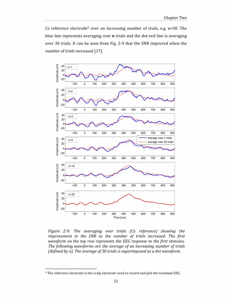
Chapter Two
22
-100 0 100 200 300 400 500 600 700 800 900
-20
0
20
40
Amplitude [uV]
-100 0 100 200 300 400 500 600 700 800 900
-20
0
20
40
Amplitude [uV]
-100 0 100 200 300 400 500 600 700 800 900
-20
0
20
40
Amplitude [uV]
-100 0 100 200 300 400 500 600 700 800 900
-20
0
20
40
Amplitude [uV]
-100 0 100 200 300 400 500 600 700 800 900
-20
0
20
40
Amplitude [uV]
-100 0 100 200 300 400 500 600 700 800 900
-20
0
20
40
Time [ms]
Amplitude [uV]
average over n trials
average over 30 trials
n=2
n=10
n=30
n=5
n=3
n=1
Cz reference electrode9 over an increasing number of trials, e.g. n=30. The
blue line represents averaging over n trials and the dot-red line is averaging
over 30 trials. It can be seen from Fig. 2-9 that the SNR improved when the
number of trials increased [17].
9 The reference electrode is the scalp electrode used to record and plot the resultant EEG.
Figure 2-9: The averaging over trials (Cz reference) showing the
improvement in the SNR as the number of trials increased. The first
waveform on the top row represents the EEG response to the first stimulus.
The following waveforms are the average of an increasing number of trials
(defined by n). The average of 30 trials is superimposed as a dot waveform.
Chapter Two
23
On the other hand, averaging in the time domain has some limitations
and is not always recommended because it may distort or miss ERPs that are
not exactly time-locked to the stimulus onset [17].
The ERPs are described by polarity in terms of positive or negative
peaks and also by latency. Therefore, the first labels refer to polarity of the
peak (P or N) and the numbers refer to the latency in milliseconds, which is
the interval time from the stimulus onset. For example, the acronym “N200”
refers to the second negative peak that appears in the signal 200 ms from the
stimulus onset [1], [26].
Differences in ERP components can be caused by the locations on the
scalp and variations from one participant to another. Memory tasks,
habituation and the response to external stimuli can also affect ERP
components. The shape of the ERP component depends on the information
included in the stimulus and response level of the participant.
Because of the high temporal resolution of an ERP, it provides
significant and unique timing information related to the brain [25]. It is
common to have accuracy of one millisecond on the evoked brain activity,
making it an appropriate methodology for analysing perceptual and cognitive
processes; both normal and abnormal. In addition, the ERP is considered the
complement of the two imaging systems; the positron emission tomography
(PET) and the functional magnetic resonance imaging (fMRI) in human
cognition studies [28]. However, the ERP offers considerably better temporal
resolution than these other two brain imaging technologies.
For the above mentioned reasons, ERP components are considered an
important measure of cognitive activities, such as working memory and
selective attention. In addition, ERPs (and specifically the P300) are useful in
detecting dysfunction in mental disorders and neurology. There is a wide
interest in the role of P300 recordings in psychological processes [16]. Owing
to the importance of the P300 in the current work, some more details of this
ERP component are explained below.
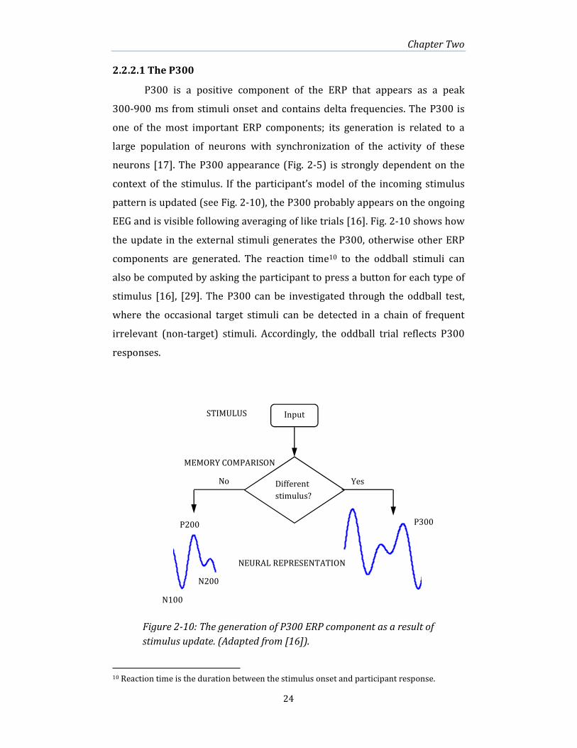
Chapter Two
24
2.2.2.1 The P300
P300 is a positive component of the ERP that appears as a peak
300-900 ms from stimuli onset and contains delta frequencies. The P300 is
one of the most important ERP components; its generation is related to a
large population of neurons with synchronization of the activity of these
neurons [17]. The P300 appearance (Fig. 2-5) is strongly dependent on the
context of the stimulus. If the participant’s model of the incoming stimulus
pattern is updated (see Fig. 2-10), the P300 probably appears on the ongoing
EEG and is visible following averaging of like trials [16]. Fig. 2-10 shows how
the update in the external stimuli generates the P300, otherwise other ERP
components are generated. The reaction time10 to the oddball stimuli can
also be computed by asking the participant to press a button for each type of
stimulus [16], [29]. The P300 can be investigated through the oddball test,
where the occasional target stimuli can be detected in a chain of frequent
irrelevant (non-target) stimuli. Accordingly, the oddball trial reflects P300
responses.
10 Reaction time is the duration between the stimulus onset and participant response.
MEMORY COMPARISON
N200
P200
Different
stimulus?
Input
Yes No
P300
N100
NEURAL REPRESENTATION
Figure 2-10: The generation of P300 ERP component as a result of
stimulus update. (Adapted from [16]).
STIMULUS
Chapter Two
25
It is believed that the component of interest, the P300, can be
measured with maximum amplitude from a specific electrode site. For
example, the midline parietal scalp sites are preferred to detect the P300.
Therefore, its recording is normally taken from the midline sites Fz, Cz and Pz
[25]. The P300 ERP has been widely used to control computer interactions
such as spelling and internet browsers [32].
2.2.2.2 The Oddball Test
The visual oddball test is a well-known method used to elicit the P300
ERP. In the oddball paradigm, a series of “target” stimuli are presented to a
participant with a chance of appearance of 10-20% e.g. the letter ‘X’ which is
called “oddball”. The common “frequent” stimuli randomly appear within the
frequent series with a chance of 80-90%, such as the letter ‘T’, and the
response to this stimulus is performed by pressing a button. When the
oddball appears, a different response is made by the participant, for example,
pressing another button. The appearance of the oddball stimuli reflects the
P300 response, which is a mark of the cognitive function [33].
2.3 EEG Connectivity between Brain Regions
Connectivity between brain regions is well known and has been an
avenue of study and research since the 1960s [30]. Identifying the
interactions and differences in activation between brain regions has been
shown in the investigations of normal and pathological brain conditions [30].
Measuring brain connectivity assesses the integration of the cerebral areas as
well. The most popular types of brain connectivity (synchrony) are the
effective connectivity and the functional connectivity. The effective
connectivity is categorized into model-based and data driven. Details are
available in [30]. The functional connectivity is divided into linear, nonlinear
and information-based methods [30].
The functional connectivity is the temporal correlation among various
neural assemblies in terms of activity [30]. The significance of the correlation
between different brain areas has been demonstrated. Neurophysiological

Chapter Two
26
waveforms such as the EEG, PET, fMRI and magneto-encephalography (MEG)
can all be assessed with the functional connectivity [30].
The linear brain functional connectivity technique refers to the cross-
correlation measure between two EEG signals, which is the one used in this
thesis. High correlation refers to strong functional connectivity between the
related pair of electrodes. To measure the functional connectivity in the
frequency domain, the following techniques are introduced: magnitude
squared coherence (MSC) for stationary signals and the wavelet coherence
(WC) for non-stationary signals. The coherence gives a measure of the
correlation between the signals within various frequency bands. In other
words, coherence gives a measure of the similarity and synchronicity
between two signals [31]. Due to the importance of the coherence measure in
the proposed work, chapter 3 presents more details on the coherence
analysis.
2.4 Summary
The EEG has been a substantial tool in providing temporal information
on the functionality of the brain. It is a low-priced (relative to other brain
imaging technologies) and simple brain activity recording method which
efficiently captures the weak electrical energy generated by the brain. The
EEG was classified into five basic frequency bands. These bands roughly
reflect various mental activities and can be measured from the scalp at
different brain sites according to the electrode placement system used. Prior
to recording, signal amplification and noise filtering are essential to prepare
the EEG for analysis. The ERP components, specifically the P300, can be
extracted from the EEG and used as a measure of cognitive activities by, for
example, presenting a participant to external stimuli. The functional
connectivity between two brain sites can be computed as a power and phase
difference using linear synchronization methods. One of these linear methods
is the wavelet coherence, which is presented in the next chapter with the
commonly used methods for EEG analyses.

Chapter Two
27
2.5 References
1
2
3
4
E. Niedermeyer and F. L. D. Silva, “Electroencephalography: Basic Principles,
Clinical Applications, and Related Fields,” Fifth ed. Philadelphia: by
Lippincott Williams & Wilkins, 2005.
J. Elshout and G. G. Molina, "Review of Brain-Computer Interfaces based on
the P300 evoked potential," Lancet Neurol, vol. 7, pp. 1032-1043, 2008.
J. R. Wolpaw, N. Birbaumer, D. J. McFarland, G. Pfurtscheller, and T. M. Vaughan,
"Brain-computer interfaces for communication and control," Clinical
Neurophysiology, vol. 113, pp. 767-791, 2002.
G. Pfurtscheller and R. Scherer, "Brain-computer interfaces used for virtual
reality control," Proceedings of the ICABB, 2010.
5 M. Teplan, "Fundamentals of EEG measurement," Measurement Science
Review, vol. 2, 2002.
6 C. D'Avanzo, V. Tarantino, P. Bisiacchi, and G. Sparacino, "A wavelet
methodology for EEG time-frequency analysis in a time discrimination
task," International Journal of Bioelectromagnetism, vol. 11, pp. 185-188, 2009.
7 Wikipedia, the free Encyclopedia, URL: http://en.wikipedia.org/wiki/Cerebral_cortex , Accessed: 20-1-2013.
8 A. Despopoulos and S. Silbernagl, “Color Atlas of Physiology”, 5th Edition ed.
Stuttgart and New York: Thieme, 2003
9 Immrama institute, “Brainwave technology for health and wellness”. URL:
http://www.immrama.org/eeg/electrode.html , Accessed: 18-4-2011.
10 N. Spitzer, D. B. Parfitt, and P. Camp. “Brain Facts” (Sixth edition). URL: http://www.sfn.org/index.aspx?pagename=brainfacts. , 2008, Accessed: 2-5-
2011.
11 M. Catani, F. Dell’Acqua, F. Vergani, F. Malik, H. Hodge, P. Roy, R. Valabregue, and M. Thiebaut de Schotten, "Short frontal lobe connections of the human
brain," Cortex, vol. 48, pp. 273-291, 2011.
12 J. M. Fuster, "Cortex and memory: emergence of a new paradigm," Journal of
cognitive neuroscience, vol. 21, pp. 2047-2072, 2009.
13 F. Sundram, Q. Deeley, S. Sarkar, E. Daly, R. Latham, M. Craig, M. Raczek, T. Fahy, M. Picchioni, and G. J. Barker, "White matter microstructural abnormalities
in the frontal lobe of adults with antisocial personality disorder," Cortex,
vol. 48, pp. 216-229, 2012.
Chapter Two
28
14 M. Krause, N. Mahant, K. Kotschet, V. S. Fung, D. Vagg, C. H. Wong, and J. G. L. Morris, "Dysexecutive behaviour following deep brain lesions–A different
type of disconnection syndrome?," cortex, vol. 48, pp. 97-119, 2012.
15 S. Dehaene, M. Kerszberg, and J. P. Changeux, "A neuronal model of a global
workspace in effortful cognitive tasks," Proceedings of the National Academy
of Sciences, vol. 95, 1998, pp. 14529-14534.
16 D. E. J. Linden, "The P300: where in the brain is it produced and what it
does it tell us?," The Neuroscientist, vol. 11, pp. 563-576, 2005.
17 A. Mouraux and G. Iannetti, "Across-trial averaging of event-related EEG
responses and beyond," Magnetic resonance imaging, vol. 26, pp. 1041-1054,
2008.
18 K. Najarian and R. Splinter, “Biomedical Signal And Image Processing,” CRC
press, 2012.
19 W. O. Tatum, A. M. Husain, S. R. Benbadis, and P. W. Kaplan, “Handbook of EEG
Interpretation,” 1 st ed. New York: Demos Medical Publishing, 2008.
20 G. H. Klem, H. Lüders, H. Jasper, and C. Elger, "The ten-twenty electrode
system of the International Federation," Recommendations for the Practice of
Clinical Neurophysiology: Guidelines of the International Federation of Clinical
Neurophysiology,(G., Deuschal, and A. Eisen, eds.), Elsevier, Amsterdam, pp. 3–6,
1999.
21 P.L Nunez, “Neocortical Dynamics and Human EEG Rhythms”, New York: Oxford Univ. Press, 1995.
22 M. Hunter, R. Smith, W. Hyslop, O. Rosso, R. Gerlach, J. Rostas, D. Williams, and
F. Henskens, "The Australian EEG database," Clinical EEG and neuroscience,
vol. 36, pp. 76-81, 2005.
23 U. Melia, F. Claria, M. Vallverdú, and P. Caminal, "Removal of peak and spike noise in EEG signals based on the analytic signal magnitude," in
Engineering in Medicine and Biology Society (EMBC), 2012 Annual International
Conference of the IEEE, 2012, pp. 3523-3526.
24 W. Y. Hsu, "Wavelet-coherence features for motor imagery EEG analysis
posterior to EOG noise elimination," IJICIC, vol. 9, 2013.
25 T. C. Handy, Ed., “Event-Related Potential A Methods Handbook,”. London:
Massachusetts Institute of Technology, 2005.
26 M. Fabiani, G. Gratton, and M. G. H. Coles, "Event-Related Potentials: methods, theory, and applications," in Handbook of Psychophysiology, C. J., et
al., Eds., ed New York: Cambridge University Press, 2000.
27 J. Elshout and G. G. Molina, "Review of Brain-Computer Interfaces based on the P300 evoked potential," Lancet Neurol, vol. 7, pp. 1032-1043, 2008.
28 D. Novak, L. Lhotska, V. Eck, and M. Sorf, "EEG and VEP Signal Processing,"
Prague 2001.

Chapter Two
29
29 A. Varnavas and M. Petrou, "Human's Performance Prediction with Wavelet
Analysis of EEG Data," in Digital Signal Processing, 2007 15th International
Conference on, 2007, pp. 167-170.
30 V. Sakkalis, "Review of advanced techniques for the estimation of brain
connectivity measured with EEG/MEG," Computers in Biology and Medicine,
vol. 41, pp. 1110-1117, 2011.
31 M. A. Guevara and M. Corsi-Cabrera, "EEG coherence or EEG correlation?,"
International Journal of Psychophysiology, vol. 23, pp. 145-153, 1996.
32 C. C. Postelnicu and D. Talaba, “P300-Based-neural computer interaction
for spelling applications,” Biomedical Engineering, IEEE Transactions on, vol.
60, pp. 534-543, 2013.
33 S. A. Huettel and G. McCarthy, “What is odd in the oddball task?: Prefrontal
cortex is activated by dynamic changes in response strategy,”
Neuropsychologia, vol. 42, pp. 379-386, 2004.

Chapter Three
30
Chapter 3
Theory of Signal Analysis and
Applications
For several decades, signal processing techniques have been widely
used to scrutinise the EEG. Considerable applications in the field of signal
processing have been developed and utilized for representing the EEG in
many different forms; including feature detection, biofeedback techniques,
diagnosis packages and BCI applications. Such applications are based on
various algorithms in the field of signal processing which manipulate the EEG
either in its original time domain form or convert the EEG into another form
such as the frequency domain. This chapter reviews some signal processing
methods that are relevant to the current work including signal analysis and
transformations followed by image quality techniques at the end of the
chapter. These image quality techniques are used in both Chapter 6 and 7 to
provide objective measures for wavelet scalogram comparisons produced by
the same signal processing algorithms in both Matlab software and FPGA
platform computations.
In this research, the applied method for data analysis and hardware
computations is called the wavelet transform (WT) or, more specifically, the
continuous wavelet transform (CWT). This technique has been widely used in
many signal processing and mathematical applications since the late 1980s
[1]. In the WT, the input signal is represented in the time-frequency plane
using special types of filters called wavelets. The WT is briefly presented in
this chapter in addition to other transform techniques that have been utilized
in the field of EEG signal processing. The flexibility and advantages of wavelet

Chapter Three
31
processing are outlined and more attention to the wavelet coherence is also
given. The computation of the wavelet analysis can be considerable and
significant optimization is needed to prepare for the possible application of
biofeedback in real time. One of the principle aims of the implementation is
to provide for this in later developments. Hence, this is the reason for
repeated references to the computational load and the use of efficient
algorithms in the hardware design detailed in Chapter 6.
In a digital hardware design, discrete signals are usually converted to
digital form. Digital signals are the result of approximated samples of discrete
signals to a certain quantization level [2]. Figure 3-1 shows the discrete and
digital representation for the same signal. A sufficient quantization level is
usually needed for appropriate representation of the signal in the digital
word form and to mitigate the produced quantization error during the
processing steps undertaken on the signal [2].
0 5 10 15 20 25 30 35 40 45 50-20
-10
0
10
20
30
40
Time(b) digital
Amplitude
0 5 10 15 20 25 30 35 40 45 50-20
-10
0
10
20
30
40
Time(a) discrete
Amplitude
Figure 3-1: Two different forms for the same signal. (a) Discrete. (b) Digital.

Chapter Three
32
One of the best known signal processing methods Fourier analysis has
a considerable amount of discussion since it provides the means of hardware
based wavelet analysis in chapters 6 and 7 of this thesis.
3.1 Fourier Analysis
3.1.1 Fourier Series
In 1822, Fourier published his theory in an application of heat (“The
Analytic Theory of Heat”) when he derived what has come to be known as the
Fourier series [3]. Thereafter, the Fourier series took its place as a basic
technique in many fields, particularly in the field of signal analysis. The idea
of Fourier analysis is to convert a function or a signal from one domain to
another. That is, converting from the time domain into the frequency domain
or converting from the spatial domain into the spectral domain.
Transforming the signal to the target domain returns several advantages that
cannot be evident when the signal was in its original domain. This allows for
making salient different information from the signal or the function and
allows for simplifying complex operations as well. For example, the complex
convolution in the time domain can be treated as a simpler multiplication
operation in the frequency domain [4].
The Fourier series states that a periodic function f(t) of period T, can
be represented by a sum of sine and cosine functions. The sum of these
functions is weighted and gives an approximation of the signal f(t). The
function of the Fourier series is formed by the coefficients Ck. The
mathematical representation of a periodic function in the Fourier series is:
�(�) = � ��� !"#$%&'$ (3-1)
where (� in the complex exponential is for k number of harmonics given by:
)� = 2+ ,- (3-2)
The complex exponential .�(/can be represented using Euler’s formula:
� !"# = cos()��) + 4567()��) (3-3)
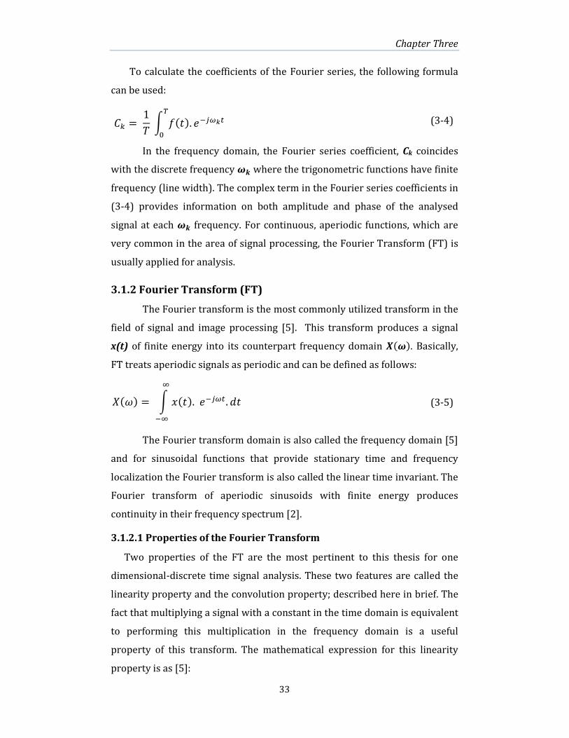
Chapter Three
33
To calculate the coefficients of the Fourier series, the following formula
can be used:
�� = 1-8 �(�). �' !"#:; (3-4)
In the frequency domain, the Fourier series coefficient, Ck coincides
with the discrete frequency (� where the trigonometric functions have finite
frequency (line width). The complex term in the Fourier series coefficients in
(3-4) provides information on both amplitude and phase of the analysed
signal at each (� frequency. For continuous, aperiodic functions, which are
very common in the area of signal processing, the Fourier Transform (FT) is
usually applied for analysis.
3.1.2 Fourier Transform (FT)
The Fourier transform is the most commonly utilized transform in the
field of signal and image processing [5]. This transform produces a signal
x(t) of finite energy into its counterpart frequency domain <((). Basically,
FT treats aperiodic signals as periodic and can be defined as follows:
=()) = 8 >(�).�' !#. ?�$'$ (3-5)
The Fourier transform domain is also called the frequency domain [5]
and for sinusoidal functions that provide stationary time and frequency
localization the Fourier transform is also called the linear time invariant. The
Fourier transform of aperiodic sinusoids with finite energy produces
continuity in their frequency spectrum [2].
3.1.2.1 Properties of the Fourier Transform
Two properties of the FT are the most pertinent to this thesis for one
dimensional-discrete time signal analysis. These two features are called the
linearity property and the convolution property; described here in brief. The
fact that multiplying a signal with a constant in the time domain is equivalent
to performing this multiplication in the frequency domain is a useful
property of this transform. The mathematical expression for this linearity
property is as [5]:

Chapter Three
34
@. A1(�) + B. A2(�) = @. C1()) + B. C2()) (3-6)
where lowercase g refers to the time domain representation and upper case
G are the relative frequency domain components. Each of a and b are
constants.
The representation of the EEG signals in digital hardware requires
biasing (scaling) these signals to values that can be manipulated in the digital
hardware design. By using (3-6), it either multiplies the EEG by a constant11
in the time domain then applies the Fourier transform or applies the Fourier
transform then multiplies it by a constant. Both methods give equivalent
products and both are used in Chapter 6 of this thesis. This shows the
usefulness of the linearity property for the work presented in Chapters 6 and
7.
The second useful property is that complex convolution between two
signals in one domain can be modified to be a simple multiplication in the
other domain. After that, the product of multiplication can be restored to the
first domain. This property can be mathematically represented as follows: A1(�) ∗ A2(�) ⟺ C1()) × C2()) C1()) ∗ C2()) ⟺ A1(�) × A2(�) (3-7)
The benefit of this property in this thesis is demonstrated in the FPGA
implementation for the CWT where it saves computations/complexity. This
will be further explained in 3.2.2.2.
3.1.2.2 Discrete Time Fourier Transform (DTFT)
The practical implementation of the continuous signals requires
modifying them into digital word form. Continuous time signals cannot be
processed inside a digital computer unless discretised at a given sampling
frequency and then automatically digitized at a suitable quantization level
[5]. The sampling frequency fsamp to a signal is reciprocal to the sampling
interval δt where:
11 The constant used in the FPGA design was 256, which then reduced to 194 to eliminate the
appearance of the overflow in the results as presented in Chapters 6 & 7 of this thesis.

Chapter Three
35
�GHIJ = 1K� (3-8)
The maximum frequency of a signal gives an idea of the suitable
sampling frequency to be used. EEG signals and other physiological signals
have relatively low frequency components compared to other signals.
Accordingly, a low sampling rate in the range 500-1000 Hz is sufficient for
the EEG where the Nyquist rate can be satisfied. The sampling process
changes the integration in (3-5) into summation:
=()) = � >(7). �' !%/MNOPQ$%&'$ (3-9)
The form of FT in (3-9) indicates that the chosen sampling frequency
binds the frequency domain of the signal. However, to digitally implement
the FT, the frequency spectrum also needs to be changed to the discrete form,
as it is still continuous in (3-9).
3.1.2.3 Discrete Fourier Transform (DFT)
The discrete Fourier transform (DFT) represents an approximation to
this transform by producing discrete frequency periods, k, to the Fourier
coefficients. These coefficients compose a sequence of the continuous
frequency spectrum. The DFT can be defined as [5]:
=(,) = � >(7). �' RS"T%U'V%&; , , = 0,…… . , Y − 1 (3-10)
whereas the inverse DFT is given by:
In the DFT, the number of points in the time domain and the
frequency domain is equal. The DFT is considered computationally a non-
efficient technique due to the large number of operations required to
complete the transform for all N points. For example, the number of complex
multiplications required in the DFT is about N2 for direct computation, which
is an extensive amount as a signal contains a large number of points [2].
>(7) = 1Y � =(,). � RS"T%U'V%&; , 7 = 0,…… . , Y − 1 (3-11)
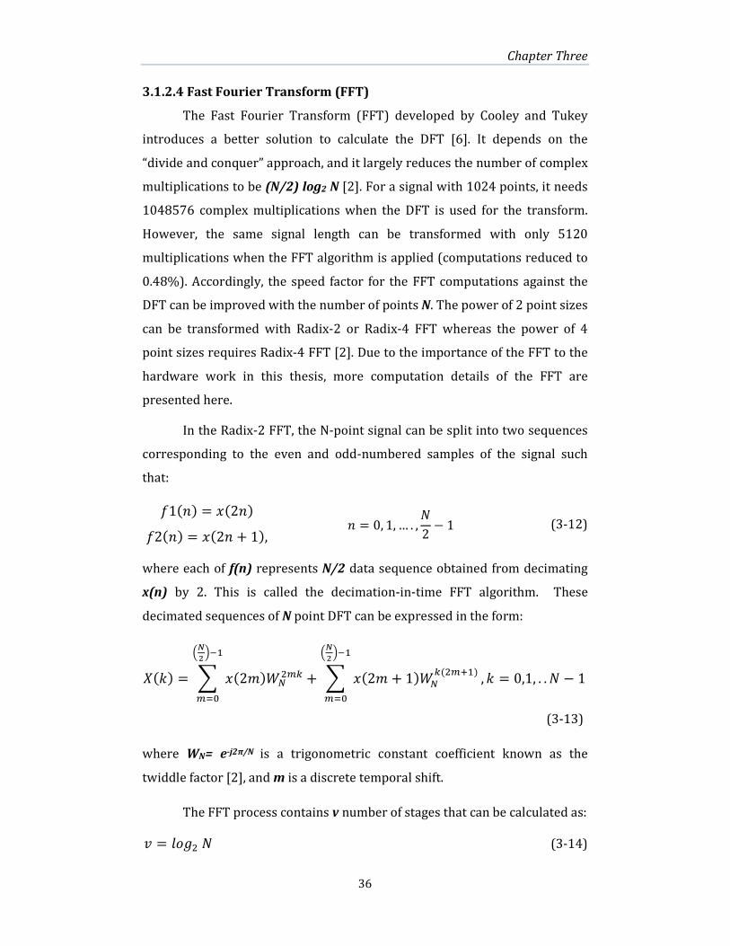
Chapter Three
36
3.1.2.4 Fast Fourier Transform (FFT)
The Fast Fourier Transform (FFT) developed by Cooley and Tukey
introduces a better solution to calculate the DFT [6]. It depends on the
“divide and conquer” approach, and it largely reduces the number of complex
multiplications to be (N/2) log2 N [2]. For a signal with 1024 points, it needs
1048576 complex multiplications when the DFT is used for the transform.
However, the same signal length can be transformed with only 5120
multiplications when the FFT algorithm is applied (computations reduced to
0.48%). Accordingly, the speed factor for the FFT computations against the
DFT can be improved with the number of points N. The power of 2 point sizes
can be transformed with Radix-2 or Radix-4 FFT whereas the power of 4
point sizes requires Radix-4 FFT [2]. Due to the importance of the FFT to the
hardware work in this thesis, more computation details of the FFT are
presented here.
In the Radix-2 FFT, the N-point signal can be split into two sequences
corresponding to the even and odd-numbered samples of the signal such
that:
where each of f(n) represents N/2 data sequence obtained from decimating
x(n) by 2. This is called the decimation-in-time FFT algorithm. These
decimated sequences of N point DFT can be expressed in the form:
=(,) = � >(2Z)[URI� + � >(2Z + 1)[U�(RI\V)]T_'VI&; , , = 0,1, . .]T_'V
I&; Y − 1 (3-13)
where WN= e-j2π/N is a trigonometric constant coefficient known as the
twiddle factor [2], and m is a discrete temporal shift.
The FFT process contains v number of stages that can be calculated as: ` = abARY (3-14)
�1(7) = >(27) �2(7) = >(27 + 1), 7 = 0, 1, … . , Y2 − 1 (3-12)

Chapter Three
37
Each stage contains N/2 number of the basic computation unit of the
FFT process, which is called the butterfly. The butterfly includes two complex
addition operations and one complex multiplication. Figure 3-2 shows the
form of this basic unit.
Due to the extensive need for the FFT in many DSP algorithms, it has
been implemented as a separate hardware core by some companies and can
be configured for the applications/modes required. Xilinx FFT V5.0 logic core
[7] is a model of these devised cores, which is used as a primary component
of the hardware wavelet design in this thesis.
A drawback of the FT is the loss of the time information. Time
information is not important for stationary signals where their frequency
contents occur at all times. For non-stationary signals, such as the EEG, using
FT is only suitable to investigate the existing spectral components in these
signals. To investigate when these spectral components occur, a time-
frequency technique needs to be used such as the short-time Fourier
transform [8].
3.1.3 Short-Time Fourier Transform (STFT)
The short-time Fourier transform (STFT) was first presented by Gabor
[10]. It permits for temporal localization in the FT by combining a window
function with the signal. This allows the estimation of the frequency
spectrum of the input signal through short overlapping windows. This is
formulized as follows:
=(c,)) = 8 >(�). d(� − c). �' !# . ?�$'$ (3-15)
WrN
a
b
-1
A= a + WrN b
B= a - WrN b
Figure 3-2: The butterfly: a basic computation unit in the FFT algorithm-
decimation in time.

Chapter Three
38
where ⍵⍵⍵⍵ denotes the frequency in the STFT plane, and τ is the temporal
location. Each of the Hanning, Hamming and Blackman functions are possible
windows to be used for improving spectral estimates [8].
The STFT has been used by researchers to overcome the weakness in
the FT. Within the chosen window, the analysed signals are assumed
stationary and the time-frequency representation can provide information on
the frequencies of the signal and the time that they occur. The STFT is a linear
time-frequency transform.
The weakness of the STFT is that it covers only a portion of the signal
since it has a finite length. Hence, good frequency resolution is produced
when the time resolution is poor, and vice versa, depending on the window
width. In addition, the selection of a finite-time interval window leads to the
problem of spectral leakage as associated with the discontinuities at the
boundaries of the window. The phenomenon of spectral leakage is detailed in
[9].
The wavelet transform was founded as a more appropriate and
accurate method for continuous spectral analysis [8], [11] such as the
continuous wavelet transforms used in this thesis. These transforms were
constructed in Fourier space by employing the FFT logic core and used to
analyse the EEG signals in FPGA.
3.2 Wavelets
In the last few decades wavelet analysis has been widely used for
signal analysis. It has the ability to decompose the signal into simple
components and analyse the temporal localization of changes in the power of
these components. Analysis using wavelet techniques provides a clear
picture of both the time and frequency components of a signal. Non-
stationary signals and signals with discontinuities have been successfully
processed with the multi-resolution WT analysis.
To perform the WT, a localized wavelet function is required. This
wavelet function is called the mother wavelet ψ(t) which can be moved
within the signal’s various locations over time in a squeezed or stretched
shape [12]-[13]. The dilation and translation of the basis wavelet function
Chapter Three
39
cope with the limitation of the fixed window in the STFT leading to the multi-
resolution analysis.
The mother wavelet function can be dilated and translated with the
two parameters s and b, to be written more compactly as:
eG,f(�) = 1√5 e g� − B5 h (3-16)
The produced daughter wavelet is,b(t) in (3-16) is achieved by scaling
the mother wavelet. The term in front of the mother wavelet is for wavelet
energy normalization.
Any finite function that satisfies the admissibility condition can be
nominated as the mother wavelet. This condition states that the mean of the
basis function must be equal to zero [4]:
The expression of the admissibility criteria is as:
�j = 8 |ψ())|R|)| ?) < ∞$'$ (3-18)
The ψ()) in the finite integral of (3-18) is the Fourier transform of the
daughter wavelet. In order to reconstruct the original signal, the finite term oi is required to be used in the inverse wavelet transform. There are various
types of wavelet functions that satisfy the admissibility condition and can be
sorted according to their characteristics.
3.2.1 Wavelet Properties
Wavelets have several properties and factors, which should be
considered in choosing the appropriate application. Some of these properties
are: orthogonal and non-orthogonal, complex or real, width of the wavelet
function and the wavelet shape (function dependent) [13]. Orthogonal
wavelet analysis implies proportionality between the convolution times at
each wavelet scale and the width of the wavelet function at that scale. This
8 e(�). ?� = 0$'$ (3-17)
Chapter Three
40
produces a change in the wavelet spectrum for the time series analysis due to
the aperiodic movement in the time series signal. Contrariwise, the non-
orthogonal wavelet function is highly redundant when the scale becomes
larger, thereby giving a highly correlated wavelet spectrum. This property is
useful for producing smooth variation in the wavelet amplitude for the time
series analysis such as the EEG. The complex form of the wavelet function is
necessary when both the amplitude and phase are required for analysis. In
addition, when the analysed signal has oscillatory behaviour, a complex
wavelet function is more suitable to capture such behaviour.
The width of the wavelet function can be defined by “the e-folding12
time of the wavelet amplitude” [13] and used to determine the resolution of
that function. Good time resolution and poor frequency resolution can be
achieved at high frequencies whereas poor time resolution and good
frequency resolution are achieved at low frequencies. Finally, the shape of
the wavelet function can be selected such that it reflects features present in
the time series. In this research, a non-orthogonal complex Morlet wavelet
function is used due to its simplicity and suitability for spectral estimations of
the EEG [11]. In the wavelet analysis, short EEG epochs of 1-2 seconds13 are
preferred especially when the sampling frequency is low. This ensures
stability of the produced features in the wavelet scalogram14 [5].
There are two classes of WTs, the continuous wavelet transform
(CWT), presented in the next section, and the discrete wavelet transform
(DWT), outlined in 3.2.3.
3.2.2 The Continuous Wavelet Transform
The continuous wavelet transform gives a continuous time-frequency
plane for the continuous input signal, X(t), as in the following equation:
12 e-folding time or “wavelet width” is relative to the wavelet scale s. It is the distance at
which a drop of 1/e2 takes place in the wavelet power, where e=2.71828 [14]. 13 The EEG epoch used in WC analysis in Chapter 5 of this thesis is 1400 ms. However, this
length is reduced to 1024 ms (multiple of 4) in Chapter 6 to be suitable for the Radix-4 FFT
core used for analysis. 14
The Scalogram is a 3-dimensional plot of time, scale & amplitude that gives the wavelet
coefficients for a time series of N samples and it shows the high power regions at a localized
time and scale. The CWT scalogram contains only positive values.
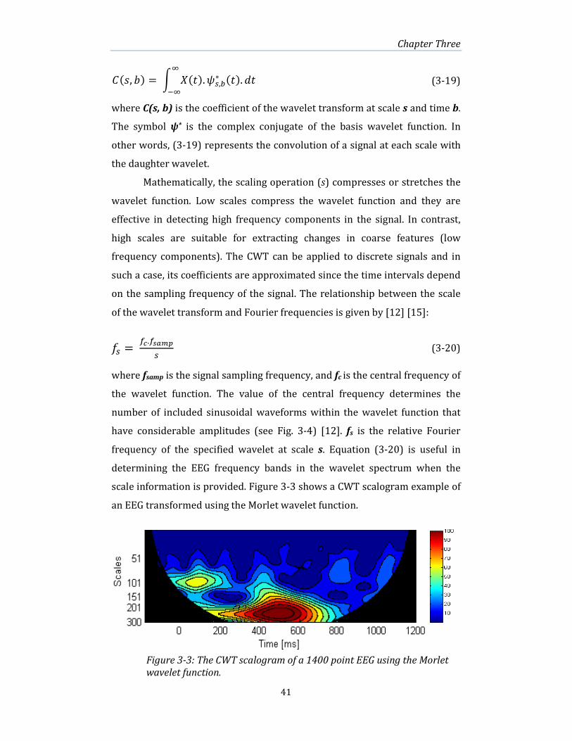
Chapter Three
41
�(5, B) = 8 =(�).eG,f∗ (�). ?�$'$ (3-19)
where C(s, b) is the coefficient of the wavelet transform at scale s and time b.
The symbol ψ* is the complex conjugate of the basis wavelet function. In
other words, (3-19) represents the convolution of a signal at each scale with
the daughter wavelet.
Mathematically, the scaling operation (s) compresses or stretches the
wavelet function. Low scales compress the wavelet function and they are
effective in detecting high frequency components in the signal. In contrast,
high scales are suitable for extracting changes in coarse features (low
frequency components). The CWT can be applied to discrete signals and in
such a case, its coefficients are approximated since the time intervals depend
on the sampling frequency of the signal. The relationship between the scale
of the wavelet transform and Fourier frequencies is given by [12] [15]:
�G = Mp.MNOPQG (3-20)
where fsamp is the signal sampling frequency, and fc is the central frequency of
the wavelet function. The value of the central frequency determines the
number of included sinusoidal waveforms within the wavelet function that
have considerable amplitudes (see Fig. 3-4) [12]. fs is the relative Fourier
frequency of the specified wavelet at scale s. Equation (3-20) is useful in
determining the EEG frequency bands in the wavelet spectrum when the
scale information is provided. Figure 3-3 shows a CWT scalogram example of
an EEG transformed using the Morlet wavelet function.
Figure 3-3: The CWT scalogram of a 1400 point EEG using the Morlet
wavelet function.

Chapter Three
42
In this scalogram, the localization in both time and frequency of the
1400 point EEG can be seen. At high scales (low frequencies), high power
wavelet coefficients are due to the P300 component occurrence. Due to the
fact that the wavelet is not completely time-localized, errors may appear
because of edge effects. This is known as the Cone of Influence (COI) and the
transform results outside the COI cannot be trusted (see Fig. 3-3 - black area).
The COI area is caused by the boundaries of the signal where discontinuity at
the edge has dropped the wavelet power to e-2 of its value [15]. The COI is
clarified in Fig. 3-3 by a black colour to recognize the region where errors
may occur.
3.2.2.1 The Morlet Wavelet Function
The complex-value Morlet wavelet function has been widely used in
the EEG analysis [11], [16]-[18]. The literature [18] by Bassani and Nievola
indicates that the Morlet wavelet is a distinctive function for feature
extraction and has perfect localization in the frequency domain. The Morlet
wavelet function has both real and imaginary parts. The central frequency of
the complex Morlet function used in this research isqr = 1 (⍵0=6) for
suitable proportion between frequency and time localization required for the
purpose of feature extraction [12], [15].
Figure 3-4 shows the shape of this function in the time domain at
different central frequencies qrand scales s. It is clear from the figure that
the change in scale compresses or stretches the function (Fig. 3-4 c & d),
while the change in the central frequency affects the number of sinusoids in
the function (Fig. 3-4 a & b). The advantage of this wavelet is that it returns
information on both the amplitude of the signal and also its phase. It can be
defined as [12]:
e(�) = +';.Rs. � RSMp#�'t^ (3-21)
This formula refers to a complex sinusoid in the term (.��uqr/)multiplied by a Gaussian envelope. The spectrum of this modulated
Gaussian permits for simple interpretation of results due to its smoothness
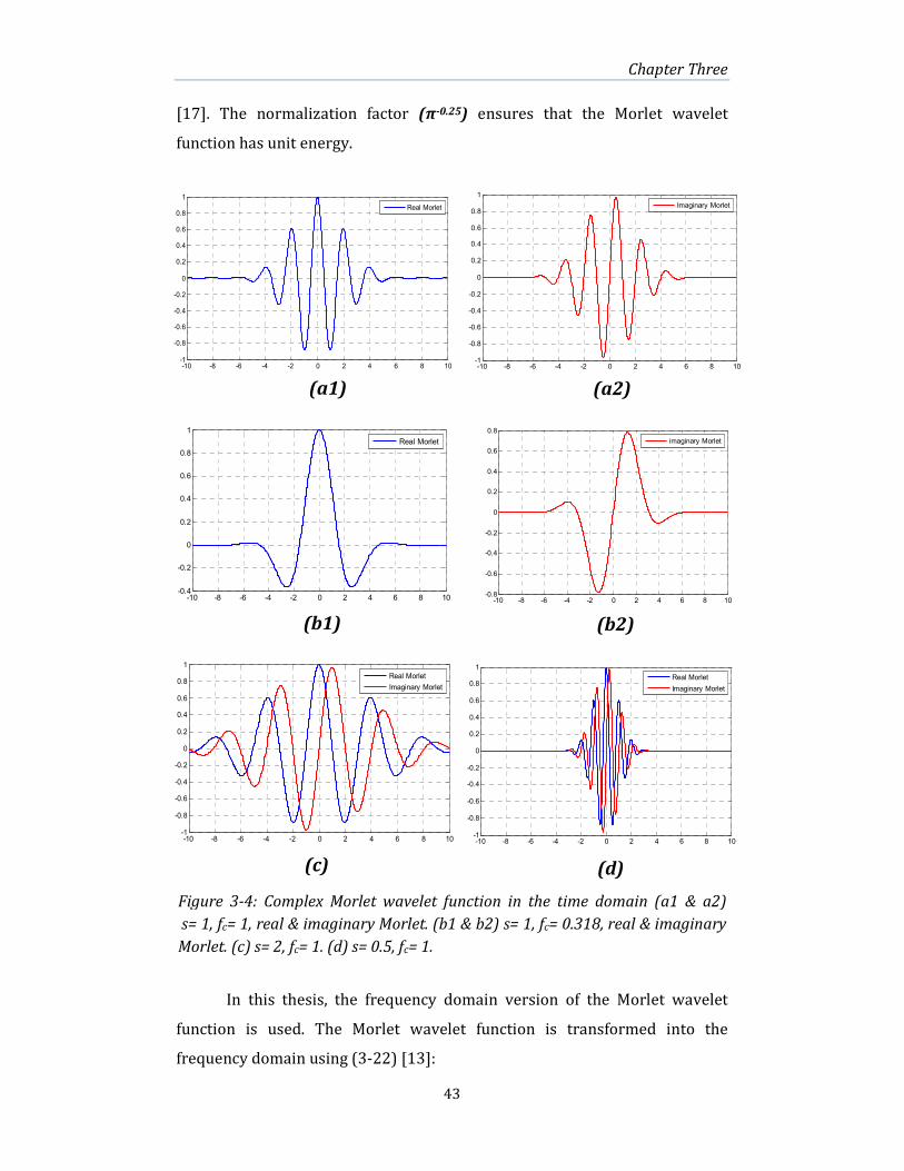
Chapter Three
43
[17]. The normalization factor (π-0.25) ensures that the Morlet wavelet
function has unit energy.
In this thesis, the frequency domain version of the Morlet wavelet
function is used. The Morlet wavelet function is transformed into the
frequency domain using (3-22) [13]:
-10 -8 -6 -4 -2 0 2 4 6 8 10-1
-0.8
-0.6
-0.4
-0.2
0
0.2
0.4
0.6
0.8
1
Real Morlet
Imaginary Morlet
-10 -8 -6 -4 -2 0 2 4 6 8 10-1
-0.8
-0.6
-0.4
-0.2
0
0.2
0.4
0.6
0.8
1
Real Morlet
Imaginary Morlet
(a2)
(b1)
(c) (d)
Figure 3-4: Complex Morlet wavelet function in the time domain (a1 & a2)
s= 1, fc= 1, real & imaginary Morlet. (b1 & b2) s= 1, fc= 0.318, real & imaginary
Morlet. (c) s= 2, fc= 1. (d) s= 0.5, fc= 1.
-10 -8 -6 -4 -2 0 2 4 6 8 10-1
-0.8
-0.6
-0.4
-0.2
0
0.2
0.4
0.6
0.8
1
Real Morlet
-10 -8 -6 -4 -2 0 2 4 6 8 10-1
-0.8
-0.6
-0.4
-0.2
0
0.2
0.4
0.6
0.8
1
Imaginary Morlet
(a1)
-10 -8 -6 -4 -2 0 2 4 6 8 10-0.4
-0.2
0
0.2
0.4
0.6
0.8
1
Real Morlet
-10 -8 -6 -4 -2 0 2 4 6 8 10-0.8
-0.6
-0.4
-0.2
0
0.2
0.4
0.6
0.8
imaginary Morlet
(b2)
Chapter Three
44
ev()) = +'V/wx()). �'(G!'!y)^/R (3-22)
where
( is the Fourier frequency at a certain scale.
�(() is the Heaviside step function, �(() = 1 if( > 0, �(() = 0
elsewhere.
Other typical types of wavelet functions that have been used in the
CWT analysis are the Paul and the Mexican hat. A brief discussion of these
two functions is presented in Chapter 6.
3.2.2.2 FFT Based CWT
One of the aims of this thesis was to optimize computations. Here the
implied convolution operations in (3-19) are complex processes to produce
the CWT. At each wavelet scale, all the samples of the input time series need
to be involved and the same is for the wavelet function. If the number of
samples is equal to J for the signal and K for the wavelet function, the total
number of linear convolutions at each scale is equal to (J+K-1). Each
convolution operation includes several steps: folding, shifting, multiplication
and summation [2]. Whereas folding is needed only once, the other three
operations are repeated at every shift step. Overall, the total number of
multiplications and additions is huge and calculating these operations in
Fourier space is much quicker. For a fixed length time series, the convolution
is feasible when applied with short wavelet sequences, e.g. some of the filters
used in the discrete wavelet transform.
For large sequences15 like the Morlet, the complex convolutions can be
replaced with simple multiplications using equation (3-7). This replacement
is conceivable when transforming both the input signal and the wavelet
function into the frequency domain. When the multiplication process is
completed at each scale, an inverse discrete Fourier transform (IDFT) can be
applied on the product to obtain the CWT coefficients. The expression to this
is as follows [13]:
15 Large sequences means that the wavelet function contains a large number of samples (a
few hundred) whereas small sequences indicates only a few samples in the wavelet filter
such as Daubechies 2, which includes 4 samples in each of its sub-bands.
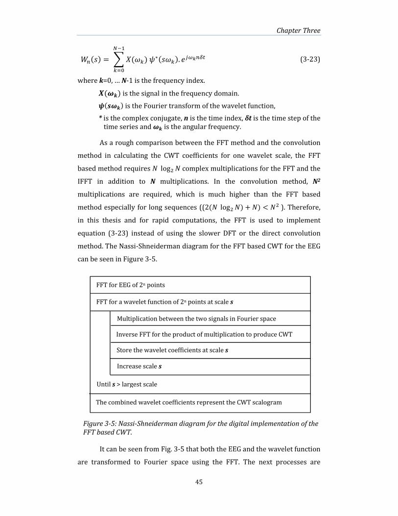
Chapter Three
45
[%(5) = � =()�)e∗(5)�). � !"%{#U'V�&; (3-23)
where k=0, … N-1 is the frequency index.
<((�)is the signal in the frequency domain.
i(�(�) is the Fourier transform of the wavelet function,
* is the complex conjugate, n is the time index, δt is the time step of the
time series and (� is the angular frequency.
As a rough comparison between the FFT method and the convolution
method in calculating the CWT coefficients for one wavelet scale, the FFT
based method requires Y logR Ycomplex multiplications for the FFT and the
IFFT in addition to N multiplications. In the convolution method, N2
multiplications are required, which is much higher than the FFT based
method especially for long sequences ((2(Y logRY) + Y) < YR). Therefore,
in this thesis and for rapid computations, the FFT is used to implement
equation (3-23) instead of using the slower DFT or the direct convolution
method. The Nassi-Shneiderman diagram for the FFT based CWT for the EEG
can be seen in Figure 3-5.
It can be seen from Fig. 3-5 that both the EEG and the wavelet function
are transformed to Fourier space using the FFT. The next processes are
Figure 3-5: Nassi-Shneiderman diagram for the digital implementation of the
FFT based CWT.
FFT for EEG of 2n points
FFT for a wavelet function of 2n points at scale s
Multiplication between the two signals in Fourier space
Inverse FFT for the product of multiplication to produce CWT
Store the wavelet coefficients at scale s
Increase scale s
Until s > largest scale
The combined wavelet coefficients represent the CWT scalogram

Chapter Three
46
multiplying their corresponding coefficients followed by taking the inverse
FFT for the product of multiplication to produce the wavelet coefficients at
scale s. By increasing the scale s and repeating these processes until the
largest scale is completed, the combined wavelet coefficients represent the
full image of the CWT scalogram. This method of calculating the CWT is
implemented in the FPGA design section (Chapter 6) of this thesis. As the
CWT represents one class of the WT, the DWT represents the other.
3.2.3 The Discrete Wavelet Transform (DWT)
The Discrete Wavelet Transform (DWT) signal analysis is different
from the CWT analysis in the computation of the coefficients where the time
and frequency periods are discrete and non-overlapped. In the DWT, the
signal is decomposed through each analysing level into frequency octaves.
Two wavelet filters are used to analyse the signal: one is low pass, ga and the
other is high pass, ha, such that [12]:
? (7) = � ℎH(Z − 27). � \V(Z)$I&'$ (3-24)
� (7) = � AH(Z − 27). � \V(Z)$I&'$ (3-25)
The two outputs are two-point decimated to produce the
approximation coefficients cj(n) and the details coefficients dj(n) at scale j .
The process is then repeated on the approximation coefficients, which retains
most of the signal information. This is illustrated in Figure 3-6 where 2 levels
of sub-band decomposition of DWT are shown.
cj(n)
cj-1(n)
dj-1(n) ha
ga 2
2 cj+1(n)
ha
ga 2
2 dj(n)
Figure 3-6: Sub-band decomposition of DWT.

Chapter Three
47
The DWT filters are relatively small in size compared to the CWT. For
example, Daubechies 4 only contains 8 coefficients for each sub-band filter
[12]. With a small number of coefficients, the convolution operation becomes
feasible. The reduction in computation complexity leads to easier
implementation in the time domain. It has been commonly used in signal
decomposition, signal de-noising, perfect reconstruction and image
compression [5]. However, the down sampling process in the DWT alters the
time shift of the input signal and produces a different group of coefficients at
the output. This makes the DWT unsuitable for some types of analysis such as
the detection of features and events in the signal [19]. The DWT is allocated
to other signal applications such as denoising or spikes detection. In the EEG
field, the DWT can be used for detecting epileptic patterns. These random
patterns are difficult to reveal when Fourier analysis is applied since they
appear infrequently and for short periods of time. In addition, Fourier
analysis does not give the occurrence time of these spikes [5].
3.2.4 Coherence Estimation
In the application of signal processing to the EEG, FT-based coherence
has been used to check for temporal variations in the coupling between
neural sources. It is a frequency-domain measure between two signals based
on their similarity [20]. According to the Oxford English Dictionary definition,
the term coherence is the action of “sticking together” or “being consistent”
[21]. Studies in the literature have referred to similar properties in
populations of neurons that, under certain conditions, can synchronize their
discharge potentials. This synchronization has been observed "between
neuronal assemblies of distant brain regions" and is called “large scale
synchronization” [22]. This matter is particularly important with respect to
distributed neuronal assemblies which have to be integrated through
complex cognitive processing [23]. Coherence computation can be applied to
study the nature of EEG signals between brain sites during the cognitive
processing of a stimulus event.
EEG coherence is defined as the coherence between pairs of
electroencephalogram signals. In other words, it is the correlation measure
between a pair of brain signals over a spectrum of frequencies. It can be

Chapter Three
48
measured from different scalp sites and provides a high time resolution
measure of the degree of dynamic connectivity between these sites [11].
3.2.4.1 Coherence Measure
A coherence measure takes on values within the amplitude range 0-1
without polarity information. When the amplitude of coherence is close to 1,
it means a high degree of similarity between the two time-series epochs.
Phase coherence is a measure of synchronicity (or time delay) between the
two time-series epochs. Coherence values for subsequent epochs rely on the
power and the phase of the two time-series along the epochs. The
information provided by coherence reflects the stability in the relationship
between a pair of signals represented by similarity (magnitude coherence)
and synchronicity (phase coherence) [24].
3.2.4.2 Magnitude Coherence
The commonly used method to estimate coupling in a pair of signals is to
compute the coherence function that can be provided by the Fourier
transform. If two signals are stationary, Fourier analysis can be used to
provide an accurate coherence measure between them. Since the EEG signals
are non-stationary, Fourier analysis is not a suitable analysing method and,
when used, ambiguous results are produced [25].
The magnitude coherence ��(q)between two stationary signals x and
y at frequency f is given by [11]:
�R(�) = ����(�)�R���(�). ���(�) (3-26)
where Sxx and Syy refer to the Fourier transform of the autocorrelation and
Sxy(f) is the cross-spectral density between the two signals x and y, which is
the Fourier transform of the cross-correlation function Rxy(τ): ���(�) = � ���(c)�' RSM�?c$'$ (3-27)
Because Sxy is a scalar product, the Schwarz16 inequality ensures that
ρ(f) takes the range from 0 to 1.
16 Schwarz inequality is the relation between two different values; considered one of the
most useful inequalities in mathematics [27].

Chapter Three
49
3.2.4.3 Wavelet Coherence
The recent use of wavelet coherence instead of Fourier coherence in
neural signals is to overcome the requirement of stationarity signals that
exist in Fourier analysis. In addition, by using Fourier methods, time
information is lost beyond phase information; for that, coherence cannot give
any information on dynamically varying or “short time” dependence between
the signals. As time resolution is essential, Fourier coherence needs to be
replaced by another method. Therefore time-frequency analysis or wavelet
analysis has been established.
The wavelet coherence is given by firstly defining the wavelet cross-
spectrum (WCS) between the wavelet transforms of two signals x and y
around scale s and time index n [15]: [%��(5) = [%�(5).[%�∗(5) (3-28)
where ��∗(�) is the complex conjugate of the wavelet transform��(�), and ���(�) refers to the wavelet cross spectrum (WCS) between x and y. Finally,
and similar to (3-26), the square wavelet coherence (WC) �� of two equal
length signals can be defined as [15], [26]:
�%R(5) = �� ]5'V[%��(5)_�R�(5'V|[%�(5)|R). � ]5'V�[%�(5)�R_
(3-29)
|���|�and�����refer to the wavelet auto-spectrum, the factor s-1 is
for converting to an energy density and S is the smoothing operator in time
and scale such that �([) = �G�H��(�#�I��[%(5)�). The role of smoothing (S) is
to improve the reliability of the spectral estimates since their degree of
variability is high (as it averages the adjacent coefficients), otherwise one
investigates power in a single point in the time-scale plane. Consequently,
numerator and denominator become similar and the WC value will be
trivially equal to one for any two epochs. The application of smoothing
ensures the WC is in the range 0-1 according to Schwarz inequality [11], [15].
The definition of WC indicates that the high magnitude coherency
(close to 1) can be obtained when the similarity between the two signals is

Chapter Three
50
high [11], [15]. This similarity can be objectively computed from the values of
both signals at each location. The following example illustrates how the
magnitude coherence measure improves between two vectors according to
their similarity. In this example, assume two same-length vectors, each of 14
elements in four different cases (as Table 3-1 shows). The different pairs
between x and y are put in gray shaded cells. The values of vector x are
changed for each further case to be similar to those in vector y. The
magnitude coherence measure is increased according to that change and
when both vectors are exactly the same, the coherence measure is equal to 1.
It can be noticed from the table that similarity between larger weight
numbers has a wide impact on the coherence result compared with smaller
numbers. For example, in case 2, the matching between several numbers in x
and y has improved the coherence measure by about 0.32 compared with
case 1, whereas in case 3, only the matching between two additional pairs
produces a much better improvement in coherence between the two vectors.
This refinement comes from the index number 14 when it rises from 5 to 30.
Table 3-1: Example of the coherence measure between two-14 element vectors
(x & y) in four different cases where x becomes closer to y for case 1 towards
case 4. The coherence result can be seen in the last row.
Case1 Case2 Case3 Case4
Index x y x y x y x y
1 11 2.2 2.2 2.2 2.2 2.2 2.2 2.2
2 1 8 8 8 8 8 8 8
3 5 6 6 6 6 6 6 6
4 2 3 3 3 3 3 3 3
5 2 8 2 8 8 8 8 8
6 8 8.9 8.9 8.9 8.9 8.9 8.9 8.9
7 31 4 4 4 4 4 4 4
8 11 4.55 4.55 4.55 4.55 4.55 4.55 4.55
9 14 4 4 4 4 4 4 4
10 12 4 4 4 4 4 4 4
11 17 3 3 3 3 3 3 3
12 6 3 6 3 6 3 3 3
13 8 3 3 3 3 3 3 3
14 5 30 5 30 30 30 30 30
Coherence
measure
0.1777 0.4980 0.9930 1.0000

Chapter Three
51
Time [ms]
Frequency [Hz]
0 200 400 600 800 1000 1200
2
3
7
15
30
60
120
0.1
0.2
0.3
0.4
0.5
0.6
0.7
0.8
0.9
Figure 3-7 shows an example of the contour WC (coherogram)
between two EEG signals, each of 1400 points recorded through the oddball
test from the sites Fz and Cz. Only the EEG frequency band regions are
displayed. The high power WC value is represented by the dark red colour,
indicating high similarity between the EEG signals in a certain wavelet plane
region. It is clear from this figure that high coherence is concentrated in the
delta EEG band (0.5-4 Hz), which reflects high coherency between the two
EEGs due to the P300 appearance. The COI area is represented by the blue
colour.
3.2.4.4 Wavelet Phase Coherence
Phase coherence is an expansion of coherence that shows the phase-
relationship between two processes. The phase difference of wavelet
coherency can be calculated from the cross-spectrum product, and it is
defined by [28]:
��(�) = �@7'V � �I(����)��H�������� (3-30)
where ���is the wavelet cross-spectrum of x and y signals.
The phase difference is a function of both time and scale. A complex
wavelet function must be used to obtain phase information with the range of
Figure 3-7: Wavelet coherence example between two EEG signals

Chapter Three
52
the phase coherence being between –π to π in radians inside the contour of
the time-frequency domain (the coherogram). Zero in phase between two
processes indicates high synchronicity between them [29]. Phase wavelet
coherence is usually represented by small arrows in the contour where in-
phase arrows point right and the anti-phase arrows point left [15]. Only
magnitude wavelet coherence is applied in this thesis.
3.2.5 Applications of CWT & WC
In the area of signal processing, there are considerable applications
that have benefitted from analysis using the continuous wavelet transform
and wavelet coherence. As mentioned earlier, the CWT provides an
outstanding approach to spectral analysis. The wavelet coherence measure
shows the correlation between a pair of non-stationary signals at a specific
time. The strength of the wavelet technique has been shown in various forms
of time series signals. It was applied to geophysical time series to test the
relation between the extension of ice in the Baltic Sea and winter over more
than 100 years [15]. The flexibility of the time-frequency localization in the
CWT can be used for estimating a target’s motion in wideband sonar systems
[30]. The CWT has also been applied to the ECG and EEG using a diversity of
methods [31]. The application of the WC to estimate the connectivity
between a pair of EEG epochs [11], [29] was used for detecting brain
abnormality in schizophrenic patients [32]. In addition, it found its way into
recent potentials such as BCI and human performance monitoring fields [18],
[33]-[34]. As the amount of data produced in analysing the EEG using the
CWT and WC are usually large [17], the involvement of statistical analysis
methods to interpret these data is common [32], [34]-[35].
The WC is required for non-stationary signals to obtain the correlation
in a pair of these signals at a localized time and scale. This correlation cannot
be detected by using the WCS when the common power of the time series is
low [15]. The application of the WC to the ERP period and specifically in the
gamma band has not been deeply investigated. The relation of the WC to
cognition and quantifying best brain channels for WC analysis deserves
further research. In addition, the processing of the WC with minimal delay
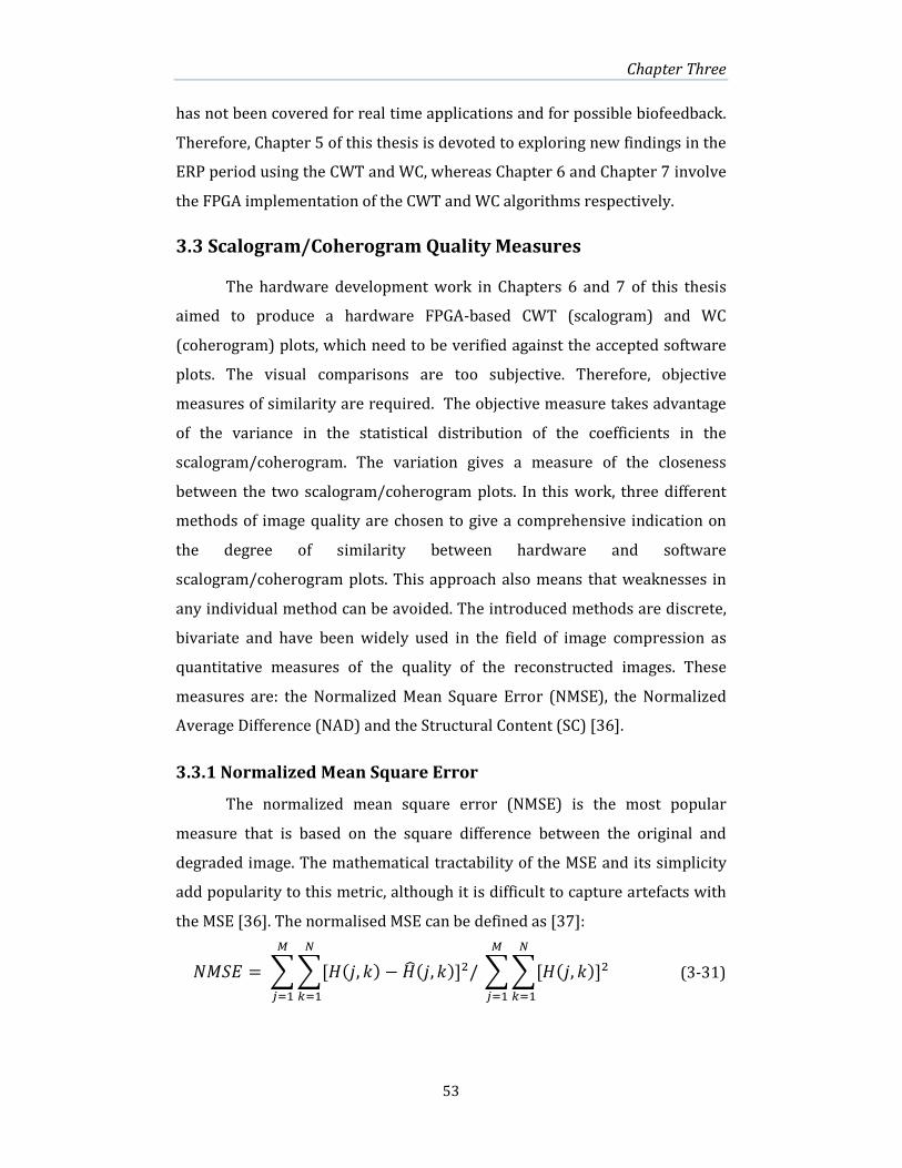
Chapter Three
53
has not been covered for real time applications and for possible biofeedback.
Therefore, Chapter 5 of this thesis is devoted to exploring new findings in the
ERP period using the CWT and WC, whereas Chapter 6 and Chapter 7 involve
the FPGA implementation of the CWT and WC algorithms respectively.
3.3 Scalogram/Coherogram Quality Measures
The hardware development work in Chapters 6 and 7 of this thesis
aimed to produce a hardware FPGA-based CWT (scalogram) and WC
(coherogram) plots, which need to be verified against the accepted software
plots. The visual comparisons are too subjective. Therefore, objective
measures of similarity are required. The objective measure takes advantage
of the variance in the statistical distribution of the coefficients in the
scalogram/coherogram. The variation gives a measure of the closeness
between the two scalogram/coherogram plots. In this work, three different
methods of image quality are chosen to give a comprehensive indication on
the degree of similarity between hardware and software
scalogram/coherogram plots. This approach also means that weaknesses in
any individual method can be avoided. The introduced methods are discrete,
bivariate and have been widely used in the field of image compression as
quantitative measures of the quality of the reconstructed images. These
measures are: the Normalized Mean Square Error (NMSE), the Normalized
Average Difference (NAD) and the Structural Content (SC) [36].
3.3.1 Normalized Mean Square Error
The normalized mean square error (NMSE) is the most popular
measure that is based on the square difference between the original and
degraded image. The mathematical tractability of the MSE and its simplicity
add popularity to this metric, although it is difficult to capture artefacts with
the MSE [36]. The normalised MSE can be defined as [37]:
Y��� = ��[x(4, ,) − x�(4, ,)]R/��[x(4, ,)]RU�&V �
&VU
�&V� &V (3-31)
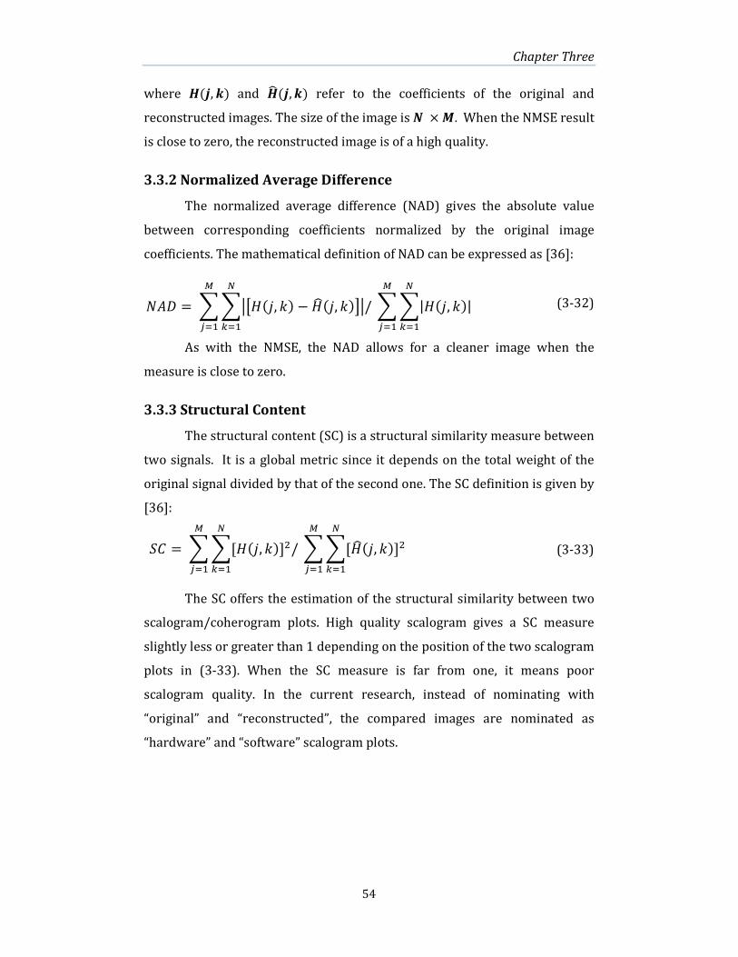
Chapter Three
54
where �(�, �) and ��(�, �) refer to the coefficients of the original and
reconstructed images. The size of the image is � �. When the NMSE result
is close to zero, the reconstructed image is of a high quality.
3.3.2 Normalized Average Difference
The normalized average difference (NAD) gives the absolute value
between corresponding coefficients normalized by the original image
coefficients. The mathematical definition of NAD can be expressed as [36]:
Y� = ���¡x(4, ,) − x�(4, ,)¢�/��|x(4, ,)|U�&V
� &V U
�&V� &V (3-32)
As with the NMSE, the NAD allows for a cleaner image when the
measure is close to zero.
3.3.3 Structural Content
The structural content (SC) is a structural similarity measure between
two signals. It is a global metric since it depends on the total weight of the
original signal divided by that of the second one. The SC definition is given by
[36]:
�� = ��[x(4, ,)]R/��[x�(4, ,)]RU�&V
� &V
U�&V
� &V (3-33)
The SC offers the estimation of the structural similarity between two
scalogram/coherogram plots. High quality scalogram gives a SC measure
slightly less or greater than 1 depending on the position of the two scalogram
plots in (3-33). When the SC measure is far from one, it means poor
scalogram quality. In the current research, instead of nominating with
“original” and “reconstructed”, the compared images are nominated as
“hardware” and “software” scalogram plots.

Chapter Three
55
3.4 Summary
This chapter has presented background for understanding the
employed signal processing techniques of the EEG in this thesis. The wavelet
technique and implications were discussed and the outstanding aspects of
the wavelet transform over the Fourier transform have been covered. The
applied FFT based CWT algorithm in producing the wavelet coefficients was
presented since it is the implemented technique in Chapter 6 for the wavelet
engine design. The wavelet coherence concept was also outlined with a
simple example about the variation of coherence between two equal-length
vectors. Some image quality methods are mentioned for later use (for
investigating the accuracy of the CWT scalogram based on the FPGA). The
next chapter gives a brief presentation on the hardware concepts required in
this research.

Chapter Three
56
3.5 References
1 S. Mallat, “A Wavelet Tour of Signal Processing”, Academic Press, San Diego,
1998.
2 J. G. Proakis and D. G. Manolakis, “Digital Signal Processing: Principles,
Algorithms, and Applications”, Fourth Ed., Prentice-Hall, Upper Saddle River, New Jersey, 2007.
3 J. Fourier, “Theorie analytique de la chaleur”, Paris, 1822.
4 J. C. Goswami and A. K. Chan, “Fundamentals of Wavelets: Theory,
Algorithms and Applications”, Wiley & Sons, New York, 1999.
5 K. Najarian and R. Splinter, “Biomedical Signal and Image Processing”,
Taylor & Francis Group, Boca Raton, 2012.
6 J. W. Cooley and J. W. Tukey, “An Algorithm for the Machine Computation of
Complex Fourier Series”, Mathematics of Computation, Vol. 19, pp.297-301,
1965.
7 The Xilinx Fast Fourier Transform core data sheet v5.0, URL: crkit.orbit-lab.org/export/4/doc/trunk/.../Xilinx/FFT/xfft_ds260.pdf, 2007, Accessed
14-2-2013.
8 R. L. Allen, D. W. Mills, “Signal Analysis: Time, Frequency, Scale and
Structure”, IEEE Press, Wiley & Sons, New Jersey, 2004.
9
F. J. Harris, “On the use of windows for harmonic analysis with the
discrete Fourier transform,” Proceedings of the IEEE, vol. 66, No. 1, pp. 51-
83, 1978.
10 D. Gabor, “Theory of Communication”, Journal IEE, Vol. 93, Part III, No. 26,
November, page 429-457, 1946.
11
J.-P. Lachaux, A. Lutz, D. Rudrauf, D. Cosmelli, M. L. V. Quyen, J. Martinerie, and F. Varela, "Estimating the time -course of coherence between single-trial
brain signals: an introduction to wavelet coherence," Neurophysiol Clin,
vol. 32, pp. 157-174, 2002.
12 P. S. Addison, “The Illustrated Wavelet Transform Handbook”, First ed.
Edinburgh, UK: Institute of Physics Publishing, 2002.
13 C. Torrence and G. P. Compo, "A Practical Guide to Wavelet Analysis,"
Bulletin of the American Meteorological Society vol. 79, pp. 61-78, 1998.

Chapter Three
57
14 Wavelet viewer, URL:
http://www.physics.nyu.edu/grierlab/idl_html_help/usinga8.html Accessed: 17-9-2013.
15 A. Grinsted, J. C. Moore, and S. Jevrejeva, "Application of the cross wavelet
transform and wavelet coherence to geophysical time series," Nonlinear
processes in Geophysics, pp. 561-566, 2004.
16 C. Hsiao-Lung, M. Ling-Fu, C. Pei-Kuang, and L. Ming-An, "Coherence Analyses of Event-Related Potentials Using Fourier and Wavelet Transforms," in
Neural Engineering, 2007. CNE '07. 3rd International IEEE/EMBS Conference
on, 2007, pp. 627-629.
17 A. Klein, T. Sauer, A. Jedynak, and W. Skrandies, "Conventional and wavelet
coherence applied to sensory-evoked electrical brain activity," Biomedical Engineering, IEEE Transactions on, vol. 53, pp. 266-272, 2006.
18 T. Bassani and J. C. Nievola, "Pattern recognition for brain-computer
interface on disabled subjects using a wavelet transformation," in
Computational Intelligence in Bioinformatics and Computational Biology, 2008.
CIBCB '08. IEEE Symposium on, 2008, pp. 180-186.
19 V. Bostanov, "BCI competition 2003-data sets Ib and IIb: feature
extraction from event-related brain potentials with the continuous wavelet transform and the t-value scalogram," Biomedical Engineering,
IEEE Transactions on, vol. 51, pp. 1057-1061, 2004.
20 R. Challis and R. Kitney, "Biomedical signal processing (in four parts). Part
3. The power spectrum and coherence function," Medical & biological
engineering & computing, vol. 29, p. 225, 1991.
21 J. Coulson, C. T. Carr, L. Hutchinson, and D. Eagle, "The Oxford Illustrated
Dictionary," H. M. Petter, Ed., Second ed. Glasgow: Oxford University Press,
1975.
22 P. König and W. Singer, "Visuomotor integration is associated with zero
time-lag synchronization among cortical areas," Nature, vol. 385, p. 157,
1997.
23 F. Varela, J. P. Lachaux, E. Rodriguez, and J. Martinerie, "The brainweb: phase
synchronization and large-scale integration," Nature reviews neuroscience,
vol. 2, pp. 229-239, 2001.
24 M. A. Guevara and M. Corsi-Cabrera, "EEG coherence or EEG correlation?," International Journal of Psychophysiology, vol. 23, pp. 145-153, 1996.
25 O. Vysata, A. Prochazka, and J. Kukal, "Fluctuation of complex wavelet
coefficients amplitude correlation in EEG," in Digital Signal Processing,
2009 16th International Conference on, 2009, pp. 1-5.
26 Y. Qi, V. Siemionow, Y. Wanxiang, V. Sahgal, and G. H. Yue,"Single-Trial EEG-
EMG Coherence Analysis Reveals Muscle Fatigue-Related Progressive

Chapter Three
58
Alterations in Corticomuscular Coupling," Neural Systems and
Rehabilitation Engineering, IEEE Transactions on, vol. 18, pp. 97-106, 2010.
27 Wikipedia, the free Encyclopedia, URL: http://en.wikipedia.org/wiki/Cauchy%E2%80%93Schwarz_inequality,
Accessed: 24-6-2013.
28 R. N. Romcy-Pereira, D. B. de Araujo, J. P. Leite, and N. Garcia-Cairasco, "A
semi-automated algorithm for studying neuronal oscillatory patterns: a wavelet-based time frequency and coherence analysis," Journal of
neuroscience methods, vol. 167, pp. 384-392, 2008.
29 R. Saab, M. J. McKeown, L. J. Myers, and R. Abu-Gharbieh, "A Wavelet Based Approach for the Detection of Coupling in EEG Signals," in Neural
Engineering, 2005. Conference Proceedings. 2nd International IEEE EMBS
Conference on, 2005, pp. 616-620.
30 S. Cheng, C.-H. Tseng, and M. Cole, "A novel fpga implementation of a
wideband sonar system for target motion estimation," in Reconfigurable
Computing and FPGAs, 2008. ReConFig'08. International Conference on, 2008, pp. 349-354.
31 P. S. Addison, J. N. Watson, G. R. Clegg, M. Holzer, F. Sterz, and C. E. Robertson,
"Evaluating arrhythmias in ECG signals using wavelet transforms," Engineering in Medicine and Biology Magazine, IEEE, vol. 19, pp. 104-109,
2000.
32 V. Sakkalis, T. Oikonomou, E. Pachou, I. Tollis, S. Micheloyannis, and M.
Zervakis, "Time-significant wavelet coherence for the evaluation of
schizophrenic brain activity using a graph theory approach," in
Engineering in Medicine and Biology Society, 2006. EMBS'06. 28th Annual
International Conference of the IEEE, 2006, pp. 4265-4268.
33 A. Varnavas and M. Petrou, "Human's Performance Prediction with
Wavelet Analysis of EEG Data," in Digital Signal Processing, 2007 15th
International Conference on, 2007, pp. 167-170.
34 W. Y. Hsu, "Wavelet-coherence features for motor imagery EEG analysis
posterior to EOG noise elimination," IJICIC, vol. 9, 2013.
35 T. R. Cutmore and P. Celka, "Composite Noise Reduction of ERPs Using
Wavelet, Model-Based, and Principal Component Subspace Methods,"
Journal of Psychophysiology, vol. 22, pp. 111-120, 2008.
36 S. Poobal and G. Ravindran, “The performance of fractal image
compression on different imaging using objective quality measures,”
International Journal of Engineering Science, vol. 3, pp. 525-530, 2011.
37 A. M. Eskicioglu and P. S. Fisher, "Image quality measures and their performance," Communications, IEEE Transactions on, vol. 43, pp. 2959-2965,
1995.
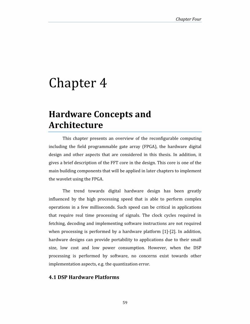
Chapter Four
59
Chapter 4
Hardware Concepts and
Architecture
This chapter presents an overview of the reconfigurable computing
including the field programmable gate array (FPGA), the hardware digital
design and other aspects that are considered in this thesis. In addition, it
gives a brief description of the FFT core in the design. This core is one of the
main building components that will be applied in later chapters to implement
the wavelet using the FPGA.
The trend towards digital hardware design has been greatly
influenced by the high processing speed that is able to perform complex
operations in a few milliseconds. Such speed can be critical in applications
that require real time processing of signals. The clock cycles required in
fetching, decoding and implementing software instructions are not required
when processing is performed by a hardware platform [1]-[2]. In addition,
hardware designs can provide portability to applications due to their small
size, low cost and low power consumption. However, when the DSP
processing is performed by software, no concerns exist towards other
implementation aspects, e.g. the quantization error.
4.1 DSP Hardware Platforms
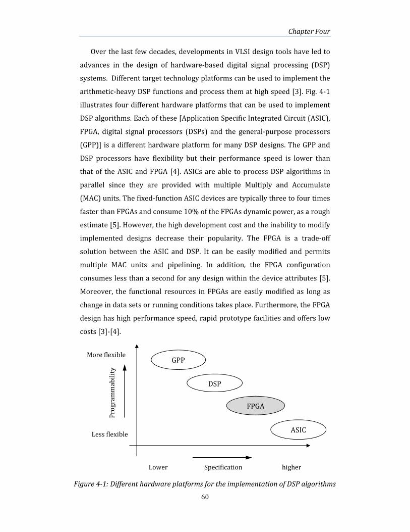
Chapter Four
60
GPP
DSP
FPGA
ASIC
Lower Specification higher
Pro
gra
mm
ab
ilit
y
Figure 4-1: Different hardware platforms for the implementation of DSP algorithms
More flexible
Less flexible
Over the last few decades, developments in VLSI design tools have led to
advances in the design of hardware-based digital signal processing (DSP)
systems. Different target technology platforms can be used to implement the
arithmetic-heavy DSP functions and process them at high speed [3]. Fig. 4-1
illustrates four different hardware platforms that can be used to implement
DSP algorithms. Each of these [Application Specific Integrated Circuit (ASIC),
FPGA, digital signal processors (DSPs) and the general-purpose processors
(GPP)] is a different hardware platform for many DSP designs. The GPP and
DSP processors have flexibility but their performance speed is lower than
that of the ASIC and FPGA [4]. ASICs are able to process DSP algorithms in
parallel since they are provided with multiple Multiply and Accumulate
(MAC) units. The fixed-function ASIC devices are typically three to four times
faster than FPGAs and consume 10% of the FPGAs dynamic power, as a rough
estimate [5]. However, the high development cost and the inability to modify
implemented designs decrease their popularity. The FPGA is a trade-off
solution between the ASIC and DSP. It can be easily modified and permits
multiple MAC units and pipelining. In addition, the FPGA configuration
consumes less than a second for any design within the device attributes [5].
Moreover, the functional resources in FPGAs are easily modified as long as
change in data sets or running conditions takes place. Furthermore, the FPGA
design has high performance speed, rapid prototype facilities and offers low
costs [3]-[4].
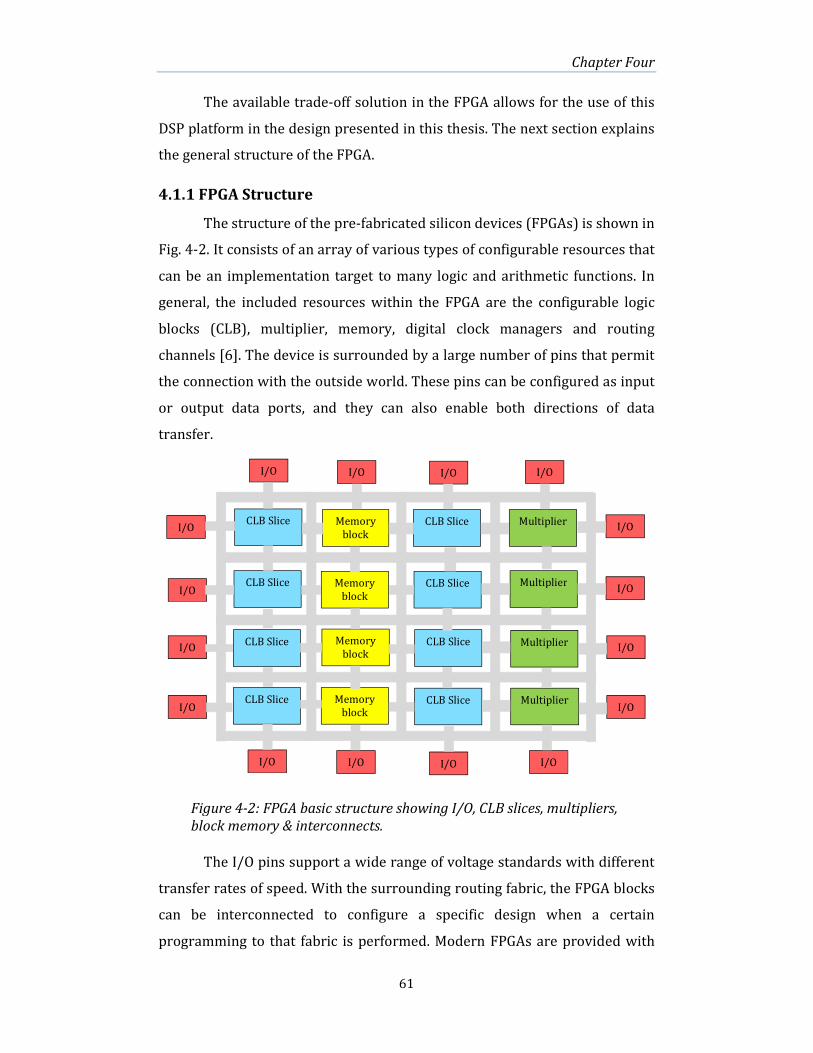
Chapter Four
61
The available trade-off solution in the FPGA allows for the use of this
DSP platform in the design presented in this thesis. The next section explains
the general structure of the FPGA.
4.1.1 FPGA Structure
The structure of the pre-fabricated silicon devices (FPGAs) is shown in
Fig. 4-2. It consists of an array of various types of configurable resources that
can be an implementation target to many logic and arithmetic functions. In
general, the included resources within the FPGA are the configurable logic
blocks (CLB), multiplier, memory, digital clock managers and routing
channels [6]. The device is surrounded by a large number of pins that permit
the connection with the outside world. These pins can be configured as input
or output data ports, and they can also enable both directions of data
transfer.
The I/O pins support a wide range of voltage standards with different
transfer rates of speed. With the surrounding routing fabric, the FPGA blocks
can be interconnected to configure a specific design when a certain
programming to that fabric is performed. Modern FPGAs are provided with
Multiplier
Multiplier
Multiplier
Multiplier
CLB Slice
CLB Slice
CLB Slice
CLB Slice
CLB Slice
CLB Slice
CLB Slice
CLB Slice
Memory
block
Memory
block
Memory
block
Memory
block
I/O I/O I/O I/O
I/O I/O I/O
I/O I/O
I/O
I/O
I/O
I/O
I/O
I/O
I/O
Figure 4-2: FPGA basic structure showing I/O, CLB slices, multipliers,
block memory & interconnects.

Chapter Four
62
either flash static memory or anti-fuse methods for the programmable
routing fabric [5].
In its basic form, the configurable logic block (CLB) consists, in turn, of
general logic components: lookup tables (LUTs), multiplexers (Mux), full
adder and D-type flip-flop as shown in Fig. 4-3. The 3-input LUT is expanded
into a 4-input LUT using a 1-bit MUX. In the arithmetic mode, the output of
the LUTs is fed to the full adder using the MUX at the middle. The final output
can be synchronous or asynchronous according to the programming of the
MUX at the right [5], [7]. The internal structure of the CLBs is different
between FPGA manufacturers. The Spartan XC3S1400AN is provided with
more than 2800 CLB slices.
The FPGA design entry can be done using a hardware description
language (HDL), graphical representation or mixing both methods such as
those designs presented in Chapter 6 and 7 in this thesis. Two popular HDL
languages are available, VHDL and Verilog [3].
Recent FPGA families are very fast with a wide range of provided
resources, and a large memory capacity. They can also be dedicated for
specific fields. Xilinx and Altera are the major manufacturers. Examples of
Xilinx FPGAs are XA Spartan-6 for automotive, Virtex-7Q and Artix-7Q for
aerospace and defence applications. The Spartan XC3S1400AN [6] with 1.4 M
gates is the one used in the present work to map the CWT design including
Figure 4-3: Generalized structure of a CLB slice. (adapted from [7]).
Clock
3-LUT
3-LUT
FA
MU
X
MU
X M
UX
D-FF
out in
a
b
c
d
Carry out
Carry in
out

Chapter Four
63
the VHDL designed controllers, as presented in Chapter 6. In Chapter 7, the
WC and the biofeedback techniques are also implemented on the same FPGA.
4.1.2 CAD Tools and HDL Design Flow
Computer Aided Design (CAD) tools provide a complete environment
for the FPGA design implementation. Many different CAD tools have been
developed that support various types of FPGAs. Typical CAD tools include
several design processes that lead to the FPGA programming by the written
HDL code [3]. These processes (Fig. 4-4) are described here in brief. The first
process is design compilation to check the HDL code for errors. If no errors
exist, the process moves on to design synthesis. An estimate to the required
FPGA resources with the timing report can be obtained from the synthesis
process. After that, the translation process generates the native generic
database (NGD) file that gives a description of the logical design. The next
process maps the contents of the NGD file into the FPGA followed by the place
and route process that routes the design and prepares for bit-stream
generation [8]. All of these processing steps need to be successfully
completed before generating the FPGA programming file. This file, when
downloaded, alters the FPGA routing fabric and configures the FPGA to the
desired design. Errors and warnings may appear during these operations
that prevent task progress unless the design entries are rectified.
In most cases, timing analyses are run following the design
implementation processes to verify the progress at that stage (as shown in
Fig. 4-5 where the CAD tool design circle is detailed [3]). This figure shows
the design circle in two types of blocks. The white blocks refer to the design
Design compilation
Synthesis Translate Mapping
Place & Route Download the
programming file (.Bit)
Figure 4-4: The design processing steps that precede the FPGA programming
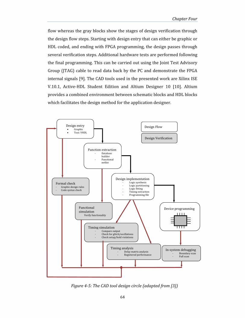
Chapter Four
64
flow whereas the gray blocks show the stages of design verification through
the design flow steps. Starting with design entry that can either be graphic or
HDL coded, and ending with FPGA programming, the design passes through
several verification steps. Additional hardware tests are performed following
the final programming. This can be carried out using the Joint Test Advisory
Group (JTAG) cable to read data back by the PC and demonstrate the FPGA
internal signals [9]. The CAD tools used in the presented work are Xilinx ISE
V.10.1, Active-HDL Student Edition and Altium Designer 10 [10]. Altium
provides a combined environment between schematic blocks and HDL blocks
which facilitates the design method for the application designer.
Figure 4-5: The CAD tool design circle (adapted from [3])
Design entry • Graphic
• Text: VHDL
Function extraction - Database
builder
- Functional netlist
Design implementation - Logic synthesis
- Logic partitioning
- Logic fitting
- Timing extraction
- Programming file
Device programming
Formal check - Graphic design rules
- Code syntax check
Functional
simulation Verify functionality
Timing simulation - Compare output
- Check for glitch/oscillations
- Check setup/hold violations
Timing analysis - Delay matrix analysis
- Registered performance
In-system debugging - Boundary scan
- Full scan
Design Flow
Design Verification

Chapter Four
65
4.2 Concepts of Digital Hardware Design
Digital signals are usually manipulated in hardware over different
arithmetic functions in a specific number system representation. The
hardware execution of the arithmetic functions can be performed either
using fixed-point or floating-point formats. Floating-point numbers require
more hardware area, and a higher speed, and they allow for a wider range of
numbers than fixed-point [3], [12]. Fixed-point representation is the most
popular in the execution of the DSP algorithms since it requires fewer
hardware resources than the floating-point numbers and supports a higher
level of accuracy.
In the fixed-point format, the first step towards any digital hardware
design is the selection of the number system representation. This is because
the processing of the numbers used is different when more than one number
system is involved in the design. The selection of the number system is also
useful in manipulating the overflow and underflow events [11]. There are
several types of number system representations in the fixed-point format; in
this work the signed integer two’s complement (2C) number representation
is applied. The popularity of the 2C comes from the possibility to add signed
numbers with no attention to any overflow in the accumulated sum as long as
it is still in the dynamic range17 [3]. The range of numbers used in this
representation can be specified as follows; if k is the number of the binary
bits per sample then the smallest and largest numbers are [3], [12]:
Smallest= −2�'V (4-1)
Largest= 2�'V − 1 (4-2)
When the used numbers exceed the range limits in (4-1) or (4-2), a
potential overflow or underflow occurs and mistaken results are produced.
In addition to the digitization of input signals, biasing18 of these signals is also
17
The dynamic range is the representation of numbers in the given range where no overflow
or underflow exists.
18 Biasing is performed by multiplying the original values (samples) with a constant.
Chapter Four
66
required to occupy the specified dynamic range and for proper operation of
the hardware design.
The hardware concepts that have an impact on the current work are:
the sample word length, timing constraints, area-speed trade-off and design
optimization. Each of these concepts is discussed in the next sections.
4.2.1 Word Length Selection
The word length represents the number of binary bits that compose
each number in the hardware design. The optimal selection of this metric has
a large impact on the requirements of the whole system [13]. The number of
bits chosen affects accuracy, dynamic range and the silicon area of the design.
A larger number of bits results in a higher accuracy of computation and low
quantization error, which leads to better results. However, when the word
length increases, the design size on the target technology becomes larger and
may negatively affect the performance speed. Small word length produces-
high quantization error thereby producing poor computation results. The
selection of the appropriate word length is a trade-off between area and
speed and it is highly influenced by the type of the signal to be analysed. The
quantization error per design stage is not calculated in the current work.
Instead, the presented image quality test in section 3.3 is applied, which gives
a global evaluation of computing accuracy by comparison with highly
accurate software results.
When the signal goes through several processing steps in a design, the
first used word length may overrun. For example, in the digital multiplication
the output size is double that of the inputs, i.e. if each of the inputs is 16 bits,
the multiplier output is 32 bits. Keeping a finite word length is necessary to
match the input size of the next stage in a design and for reducing area and
power consumption [15]. Truncation or number rounding can be applied to
keep a finite word length through the entire design [11]. For the EEG, 16 bits
is the typical word length required for the representation of the signal
samples in digital hardware [14], which is considered in the design chapters
(6 and 7) of this work.
Chapter Four
67
4.2.2 Design Critical Path and Timing Constraints
Any complex digital design involves parallel and sequential
computations. Sequential computations can be performed by separating the
combinational logics being used into multiple stages. Storage elements
(registers) are usually used to separate data between combinational logics
and are controlled by using clock pulses. These clocks are connected to the
main clock source on the main board where the target technology (e.g. FPGA)
is located. When the combinational logic has the longest path in the netlist, it
is called the critical path, which is the maximum propagation delay between
two storage elements in a design (in nanoseconds) [5]. The maximum
frequency that the design is clocked with is highly affected by the critical path
[17]. A longer path results in a reduction in the maximum frequency of
operation. Other factors that impact on the design clock rate are the clock
source and the type of target technology itself. Complex designs may have a
long critical path which forces the maximum clock source to be reduced in
order to conform to the actual timing constraints. Any increase in the
maximum frequency of operation leads to an overlap of data between the
design combinational stages and produces distorted results. One of the
methods to reduce the design critical path is to use pipeline registers [16].
Efficiently designed and written HDL code can also shorten a design critical
path [3]. In the CAD, the timing analysis tool provides information on the
design critical path following the design place and route step for FPGA design
flow [17].
The latency (in number of cycles) is the longest path between the
input and the output of a design going through the design critical path. Figure
4-6 shows both of these two indices in a simple logic example. The critical
path is the most important to be considered due to its impact on the
operational frequency.

Chapter Four
68
or1
OR2S or2
OR2S
And1
AND2S
or3
OR2S
C
D Q
D-FF1
FD
C
D Q
D-FF2
FD
C
D Q
D-FF3
FD
C
D Q
D-FF4
FD
Input4
C
D Q
D-FF5
FD
Input1
Input2
Input3
Input5
Critical path
Output1
Maximum delay (latency)
4.2.3 Area and Speed
Every target technology contains a finite amount of resources such as
the CLB slices, embedded multipliers, block RAM and a few hundred
input/output ports. Therefore, exceeding any of these resources leads to
unsuccessful design implementation. When a larger design is planned, more
resources are needed. Additional utilization of FPGA resources may be
reflected by a longer critical path thereby decreasing the operating speed,
since both of these metrics oppose each other [5]. The CAD tools give an idea
of the design size in addition to its critical path before the final FPGA
implementation. In the case of inadequate target technology for a design, a
higher resourced FPGA can be used or design optimization can be applied.
4.2.4 Design Optimization
Design optimization is quite important since it results in saving
hardware resources, increasing the operational frequency, reducing the
required area and reducing power consumption. Optimization can be
achieved through writing efficient design code and efficient processing of the
given data. In the present work, several design optimization schemes are
performed that serve the overall CWT design structure well. They also reduce
computations and resource requirements, as well as improve the speed of
operation.
Figure 4-6: A design critical path and the latency delay

Chapter Four
69
The Xilinx FFT core is a primary component of the proposed CWT
design in this thesis. For less complexity, the CWT is based on the FFT since
calculating the wavelet coefficients in the frequency domain requires
multiplications instead of using convolutions in the time domain, as
presented in Chapter 3. Hence the design of the CWT engine requires an FFT.
Therefore, the FFT core is used to transform the EEG to the frequency
domain. It is also used for the IFFT to produce the wavelet coefficients. A
more detailed presentation of this core is provided in the next section in
addition to its architectural options and control.
4.3 The Xilinx FFT Core: Configuration and Generation
A freely available FFT core from Xilinx was used in this design [18].
The Xilinx FFT core V.5 is one of the previously developed intellectual
property (IP) cores for multi-purpose usage. Each of these cores performs a
specific commonly adopted function or algorithm. The Ethernet controllers,
PCI interface, CORDIC19 and the FFT core are all examples of IP cores used in
making ASIC or FPGA for a product [19]. The FFT core has been used in
many DSP applications with different configuration schemes (e.g. Orthogonal
Frequency Division Multiplexing (OFDM) modulation technique for wireless
communication systems [20]). The FFT core is selected and used to
implement the presented algorithms in section 3.1.2.4, which provide an
efficient computation of the discrete Fourier transform (DFT). The designed
configuration can be obtained through the core generation steps. Following
the configuration process, the core is located as a VHDL component file
according to the preselected features. Once the core generation process is
completed, any desired change in the features cannot be made and a new
core has to be generated.
The Xilinx ISE 10.1 is used to generate the FFT core having different
features through the IP tool. A parent VHDL code file also needs to be written
in VHDL. This file contains a definition of the core as a “component” in the
architectural part of the code. In addition to the two VHDL files (the FFT core
19 CORDIC stands for: Coordinate Rotation Digital Computer.
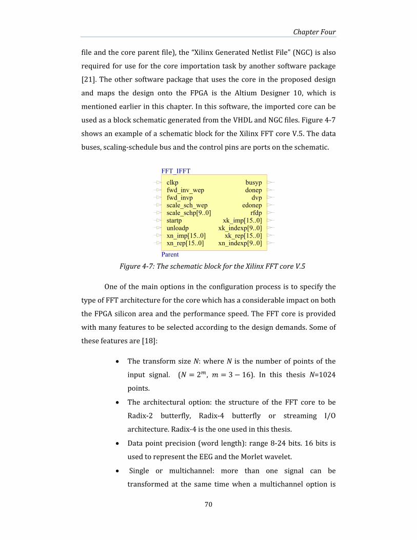
Chapter Four
70
file and the core parent file), the “Xilinx Generated Netlist File” (NGC) is also
required for use for the core importation task by another software package
[21]. The other software package that uses the core in the proposed design
and maps the design onto the FPGA is the Altium Designer 10, which is
mentioned earlier in this chapter. In this software, the imported core can be
used as a block schematic generated from the VHDL and NGC files. Figure 4-7
shows an example of a schematic block for the Xilinx FFT core V.5. The data
buses, scaling-schedule bus and the control pins are ports on the schematic.
One of the main options in the configuration process is to specify the
type of FFT architecture for the core which has a considerable impact on both
the FPGA silicon area and the performance speed. The FFT core is provided
with many features to be selected according to the design demands. Some of
these features are [18]:
• The transform size N: where N is the number of points of the
input signal. (Y = 2I, Z = 3 − 16). In this thesis N=1024
points.
• The architectural option: the structure of the FFT core to be
Radix-2 butterfly, Radix-4 butterfly or streaming I/O
architecture. Radix-4 is the one used in this thesis.
• Data point precision (word length): range 8-24 bits. 16 bits is
used to represent the EEG and the Morlet wavelet.
• Single or multichannel: more than one signal can be
transformed at the same time when a multichannel option is
Figure 4-7: The schematic block for the Xilinx FFT core V.5
clkpfwd_inv_wepfwd_invpscale_sch_wepscale_schp[9..0]startpunloadpxn_imp[15..0]xn_rep[15..0]
busypdonepdvp
edoneprfdp
xk_imp[15..0]xk_indexp[9..0]xk_rep[15..0]
xn_indexp[9..0]
FFT_IFFT
Parent

Chapter Four
71
used; however, the design area is doubled according to the
number of channels involved. A single channel is used in this
thesis to perform both the FFT and the IFFT at different times.
During the FFT computations, the data word length grows through the
butterfly unit in the core where the implied multiplications increase the bit
size. The width of the output is expressed as:
b¥�¦¥�d6?�ℎ = 67¦¥�d6?�ℎ + abAR(�§@75�b§Za�7A�ℎ) + 1 (4-3)
For example: according to (4-3), a 1024 input point with a 16 bit
sample, produces an FFT output sample of 27 bits (16 + 10 + 1 = 27).
Truncation or rounding can be used to accommodate the word length
expansion. The required type of scaling can be selected at the core
configuration step. The scaling can be done using the 10 bit scale_schp[9..0]
input port (Fig. 4-7). The scaling schedule input bus keeps the first extension
of the input word length over the internal stages of the core and also at the
output. Where insufficient scaling is used, a potential overflow may arise due
to the growth of the output beyond the specified dynamic range.
Several I/O ports are available on the core including pins and buses
that are used for data in and out, (i.e. core function), clock, core control and
status (see Table 4-1 for port width, direction and description). Some of the
provided input pins are used to control the FFT core into the intended way of
running.
The EEG used in the present thesis has a length of 1024 points
sampled at 1000 Hz and represented with a 16 bit sample. According to these
data, the core configuration here is a single 1024 point channel; Radix-420
burst I/O architecture, with 16 bit point precision. Table 4-1 shows the core
pin-out details. The following section details the possible architectural
options of the FFT core.
20 Radix-4 butterfly configuration is used in the current work among the options of Radix-2
and the pipelined architectures.
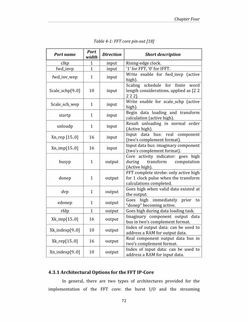
Chapter Four
72
Table 4-1: FFT core pin-out [18]
Port name Port
width Direction Short description
clkp 1 input Rising-edge clock.
fwd_invp 1 input ‘1’ for FFT, ‘0’ for IFFT.
fwd_inv_wep 1 input Write enable for fwd_invp (active
high).
Scale_schp[9..0] 10 input
Scaling schedule for finite word
length considerations, applied as [2 2
2 2 2].
Scale_sch_wep 1 input Write enable for scale_schp (active
high).
startp 1 input Begin data loading and transform
calculation (active high).
unloadp 1 input Result unloading in normal order
(Active high).
Xn_rep [15..0] 16 input Input data bus: real component
(two’s complement format).
Xn_imp[15..0] 16 input Input data bus: imaginary component
(two’s complement format).
busyp 1 output
Core activity indicator: goes high
during transform computation
(Active high).
donep 1 output
FFT complete strobe: only active high
for 1 clock pulse when the transform
calculations completed.
dvp 1 output Goes high when valid data existed at
the output.
edonep 1 output Goes high immediately prior to
“donep” becoming active.
rfdp 1 output Goes high during data loading task.
Xk_imp[15..0] 16 output Imaginary component output data
bus in two’s complement format.
Xk_indexp[9..0] 10 output Index of output data: can be used to
address a RAM for output data.
Xk_rep[15..0] 16 output Real component output data bus in
two’s complement format.
Xn_indexp[9..0] 10 output Index of input data: can be used to
address a RAM for input data.
4.3.1 Architectural Options for the FFT IP-Core
In general, there are two types of architectures provided for the
implementation of the FFT core: the burst I/O and the streaming

Chapter Four
73
architectures [18]. The desired selection can go to either higher throughput
architecture or lower FPGA resources. Burst I/O architecture can be in the
form of Radix-2 to construct a power of two FFT sequence or Radix-4 for a
power of four FFT sequence. Brief descriptions on the main features of these
architectures follow.
Radix 2 Burst I/O
In this architecture, one Radix-2 butterfly computing unit is used. The
input frame size is in the power of 2 and can be in the range 8 to 65536. The
frame is loaded first with a number of clock cycles equal to the frame size
then processing is started. The latency is longer than the size of the input
data stream. During FFT computation, no data can be loaded until completion
of the current computations. After that, the results are unloaded giving both
the FFT real and imaginary components of the signal in parallel. Data unload
consumes the same delay for data load which is equal to the frame size
(1 clock cycle/sample). Since the data load/unload and the FFT processing is
not simultaneous in burst architectures, their throughput is lower than the
streaming configuration option. However, the low usage of resources
characterizes burst architectures [18]. Fig. 4-8 shows the block diagram of
Radix-2 burst I/O architecture.
Figure 4-8: Radix-2 burst I/O FFT core architecture [18]
Data
RAM 0
Data
RAM 1
Radix-2
Butterfly
ROM for
Twiddle
s
Output data (unload)
Input data (load) Switch Switch

Chapter Four
74
It is clear from Fig. 4-8 that physically one butterfly unit has been
involved for all the FFT data-path stages of processing over several time
intervals. The twiddle factors are computed in advance before storing in the
memory. In addition, two RAMs are used to send and store the input and
output streams of data from the butterfly, as shown in Fig. 4-8. The two
switch blocks perform the transfer of these data streams. Over the switching
unit, the butterfly receives the data streams from the two memories, applies
the ith stage of computations, then writes back the intermediate calculated
results at their first locations in the RAM [22]-[23].
Radix 4 Burst I/O
The change in this architecture is that Radix-4 is the computing engine
instead of Radix-2, which covers frame sizes from 64 to 65536. Latency is
lower than Radix-2 and slightly longer than the length of the input frame. The
throughput is almost double that in Radix-2 with higher usage of hardware
resources. This architecture was chosen in the current research as a trade-off
solution between Radix-2 and the streaming counterparts. Moreover, it can
be implemented on the low cost Spartan 3AN FPGA (used in this thesis)
leaving enough room for the other components of the design. Fig. 4-9 shows
the implementation block diagram of Radix-4 burst I/O. The principle of
operation is close to that in Radix-2 adding two more random access
memories for the input data and the intermediate results [18].
Figure 4-9: Radix-4 burst I/O FFT core architecture [18]
Input data Switch Switch
Output data
Radix-4
DRAGONFLY
Data
RAM 0
Data
RAM 2
ROM for
Twiddles
Data
RAM 1
Data
RAM 3

Chapter Four
75
Streaming I/O (Pipelined)
The streaming configuration is provided with several butterfly
processing stages to allow continuous FFT processing for the input frames. In
each processing stage, there is a memory bank for both input and
intermediate data storage, which distinguishes this architecture from the
burst options. The core is able to perform simultaneous transform
computations on the existent stream of data, load a new frame and unload
the outcome of the preceding frame. In contrast, the pipelined architecture
requires a large silicon area compared with the burst options. The streaming
architecture is depicted in Fig. 4-10 including a pair of Radix-2 FFT
processors in each group. For more details on the pipelined architecture, the
reader is referred to [18], [22]-[24].
To test the located FFT core within a design schematic sheet of the
Altium designer, a VHDL based circuit is required to control the operation of
the core at high clock speed.
4.4 FFT Core Control Circuit
The operation of the FFT core requires a control circuit to initialize
the core, synchronize the transfer of data from the memory into the core,
check the core status and prepare storage for the results. In this case, VHDL
Output data
Memory Memory
Radix-2
Butterfly
Radix-2
Butterfly
Input data
Stage 0 Stage 1
Memory Memory
Radix-2
Butterfly
Radix-2
Butterfly
Group 0
Stage 2 Stage 3
Memory Memory
Radix-2
Butterfly
Radix-2
Butterfly
Group 1
Output
shuffling
Figure 4-10: Pipelined, streaming I/O FFT architecture [18]
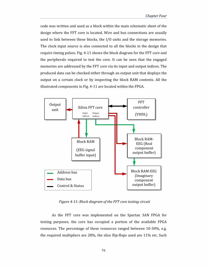
Chapter Four
76
code was written and used as a block within the main schematic sheet of the
design where the FFT core is located. Wire and bus connections are usually
used to link between these blocks, the I/O units and the storage memories.
The clock input source is also connected to all the blocks in the design that
require timing pulses. Fig. 4-11 shows the block diagram for the FFT core and
the peripherals required to test the core. It can be seen that the engaged
memories are addressed by the FFT core via its input and output indices. The
produced data can be checked either through an output unit that displays the
output on a certain clock or by inspecting the block RAM contents. All the
illustrated components in Fig. 4-11 are located within the FPGA.
As the FFT core was implemented on the Spartan 3AN FPGA for
testing purposes, the core has occupied a portion of the available FPGA
resources. The percentage of these resources ranged between 10-30%, e.g.
the required multipliers are 28%, the slice flip-flops used are 11% etc. Such
Address bus
Data bus
Control & Status
Xilinx FFT core
FFT
controller
(VHDL)
Block RAM
(EEG signal
buffer input)
Block RAM-
EEG (Real
component
output buffer)
Block RAM-EEG
(Imaginary
component
output buffer)
Output
unit
Figure 4-11: Block diagram of the FFT core testing circuit
Input
indices Output
indices
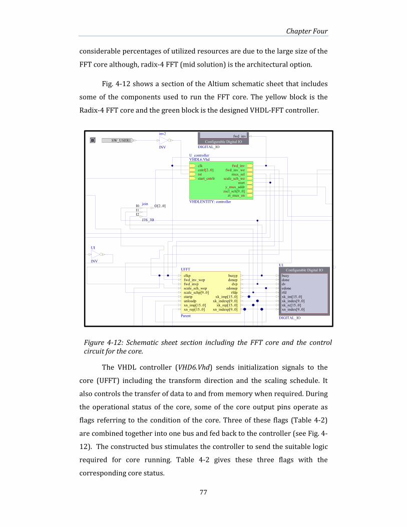
Chapter Four
77
considerable percentages of utilized resources are due to the large size of the
FFT core although, radix-4 FFT (mid solution) is the architectural option.
Fig. 4-12 shows a section of the Altium schematic sheet that includes
some of the components used to run the FFT core. The yellow block is the
Radix-4 FFT core and the green block is the designed VHDL-FFT controller.
The VHDL controller (VHD6.Vhd) sends initialization signals to the
core (UFFT) including the transform direction and the scaling schedule. It
also controls the transfer of data to and from memory when required. During
the operational status of the core, some of the core output pins operate as
flags referring to the condition of the core. Three of these flags (Table 4-2)
are combined together into one bus and fed back to the controller (see Fig. 4-
12). The constructed bus stimulates the controller to send the suitable logic
required for core running. Table 4-2 gives these three flags with the
corresponding core status.
Figure 4-12: Schematic sheet section including the FFT core and the control
circuit for the core.
clkpfwd_inv_wepfwd_invpscale_sch_wepscale_schp[9..0]startpunloadpxn_imp[15..0]xn_rep[15..0]
busypdonepdvp
edoneprfdp
xk_imp[15..0]xk_indexp[9..0]xk_rep[15..0]
xn_indexp[9..0]
UFFT
Parent
Configurable Digital IO
busydonedvedonerfdxk_im[15..0]xk_index[9..0]xk_re[15..0]xn_index[9..0]
U1
DIGITAL_IO
UI
INV
I0I1I2
O[2..0]join
J3S_3B
inv2
INV
SW_USER1 Configurable Digital IO
fwd_inv
DIGITAL_IO
clkcntrl[2..0]
fwd_invfwd_inv_we
mux_selrstscale_sch_we
startstart_cntrlr
y_mux_addrzscl_sch[9..0]
zt_mux_en
VHDLENTITY: controller
U_controllerVHDL6.Vhd

Chapter Four
78
Table 4-2: Three outputs for the FFT core status
Ready for data (rfdp) Busyp (busyp) Data valid (dvp) Core status
0 0 0 Idle
1 0 0 Loading input frame
0 1 0 Compute FFT or IFFT
0 0 1 Unload results
The xn_indexp core index for input data is very useful in generating the
required addresses for the RAM that hold the input signal to be analysed. In
the case of IFFT, the xk_indexp was added to address another RAM for the
imaginary component of the signal. These addresses precede the first input
data sample to the core by three clock cycles (as a tolerance delay) to allow
for addressing the memory and receiving the stored data.
The VHDL code was written in the Active-HDL-student edition
software package. It was verified using the provided timing simulation
waveform in the software. This is a pre-step test before transferring the code
as a block controller in the Altium main sheet.
4.5 Testing
The test of the FFT core was done on a 1024 point sine wave as a
stationary signal and then on a 1024 point real world EEG wave as a non-
stationary signal. The purpose of the test was to ensure that the EEG signal
could be transformed to the frequency domain then retransformed back to
the time domain with minimal error. Fig. 4-13 shows the original and
reconstructed sine wave by the FFT core. The scaling process due to word
length expansion produces quantization noise as the difference between the
original and reconstructed sine wave. Fig. 4-14 shows this quantization noise
with a very low amplitude compared with the amplitude of the sine wave in
Fig. 4-13.

Chapter Four
79
0 100 200 300 400 500 600 700 800 900 1000-250
-200
-150
-100
-50
0
50
100
150
200
250
Time [ms]
Amplitude
Original
Reconstructed
0 100 200 300 400 500 600 700 800 900 1000-20
-15
-10
-5
0
5
10
Time [ms]
Amplitude
Quantization noise
The same test was undertaken for an EEG signal with a P300
component. Fig. 4-15 shows the original and reconstructed EEG wave by the
core. Fig. 4-16 includes the real and imaginary components of the FFT
analysis.
The real and imaginary components of the EEG in Fig. 4-16 show a
difference in the magnitude. The high accuracy of the reconstructed EEG
signal in Fig. 4-15 proves the valid operation of the core for non-stationary
signals. The reconstructed EEG is produced from the real port (xk_rep[15..0])
when the IFFT process is completed.
Figure 4-13: The original sine wave and the reconstructed one by the FFT
core.
Figure 4-14: The produced quantization noise between the sine waves in
Fig. 4-13.
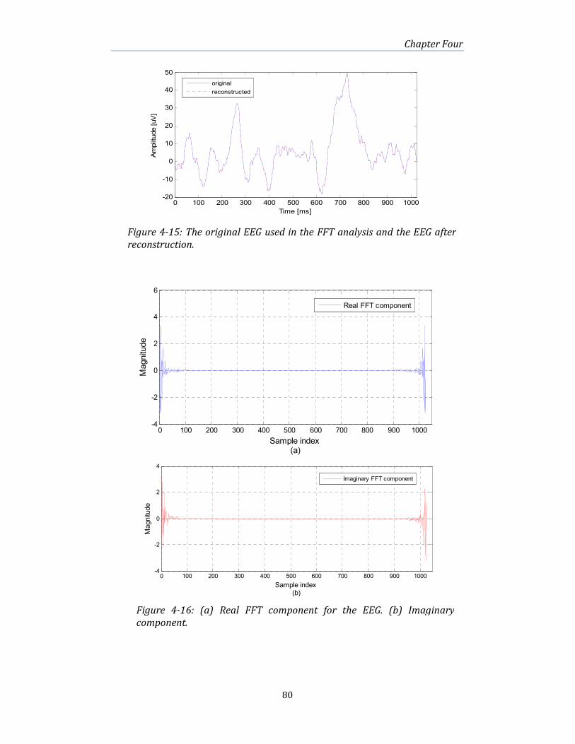
Chapter Four
80
Figure 4-16: (a) Real FFT component for the EEG. (b) Imaginary
component.
0 100 200 300 400 500 600 700 800 900 1000-4
-2
0
2
4
Sample index (b)
Magnitude
Imaginary FFT component
0 100 200 300 400 500 600 700 800 900 1000-4
-2
0
2
4
6
Sample index (a)
Magnitude
Real FFT component
Figure 4-15: The original EEG used in the FFT analysis and the EEG after
reconstruction.
0 100 200 300 400 500 600 700 800 900 1000-20
-10
0
10
20
30
40
50
Time [ms]
Amplitude [uV]
original
reconstructed
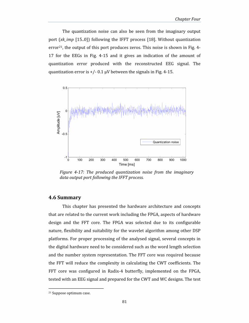
Chapter Four
81
The quantization noise can also be seen from the imaginary output
port (xk_imp [15..0]) following the IFFT process [18]. Without quantization
error21, the output of this port produces zeros. This noise is shown in Fig. 4-
17 for the EEGs in Fig. 4-15 and it gives an indication of the amount of
quantization error produced with the reconstructed EEG signal. The
quantization error is +/- 0.1 µV between the signals in Fig. 4-15.
4.6 Summary
This chapter has presented the hardware architecture and concepts
that are related to the current work including the FPGA, aspects of hardware
design and the FFT core. The FPGA was selected due to its configurable
nature, flexibility and suitability for the wavelet algorithm among other DSP
platforms. For proper processing of the analysed signal, several concepts in
the digital hardware need to be considered such as the word length selection
and the number system representation. The FFT core was required because
the FFT will reduce the complexity in calculating the CWT coefficients. The
FFT core was configured in Radix-4 butterfly, implemented on the FPGA,
tested with an EEG signal and prepared for the CWT and WC designs. The test
21 Suppose optimum case.
Figure 4-17: The produced quantization noise from the imaginary
data output port following the IFFT process.
0 100 200 300 400 500 600 700 800 900 1000-1
-0.5
0
0.5
Time [ms]
Amplitude [uV]
Quantization noise

Chapter Four
82
results of the FFT core show the operation of the core illustrated by
producing the real and imaginary components of the EEG signal in the
frequency domain. In the IFFT process, the reconstructed EEG from the real
output port of the core is of high similarity to the original one. Very low
amplitude of quantization noise is produced from the imaginary output port
of the core in the IFFT process. These results prove the ability to use the core
for non-stationary complex signals such as the EEG. The engagement of the
core in the continuous wavelet transform design is presented in Chapter 6 of
this thesis.
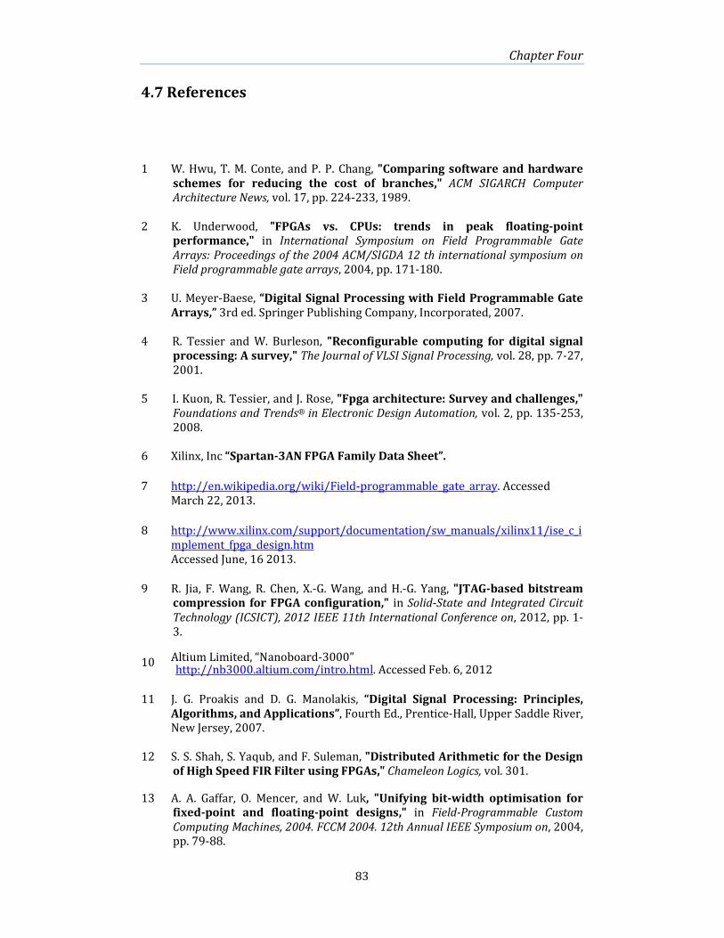
Chapter Four
83
4.7 References
1 W. Hwu, T. M. Conte, and P. P. Chang, "Comparing software and hardware
schemes for reducing the cost of branches," ACM SIGARCH Computer
Architecture News, vol. 17, pp. 224-233, 1989.
2 K. Underwood, "FPGAs vs. CPUs: trends in peak floating-point performance," in International Symposium on Field Programmable Gate
Arrays: Proceedings of the 2004 ACM/SIGDA 12 th international symposium on
Field programmable gate arrays, 2004, pp. 171-180.
3 U. Meyer-Baese, “Digital Signal Processing with Field Programmable Gate
Arrays,” 3rd ed. Springer Publishing Company, Incorporated, 2007.
4 R. Tessier and W. Burleson, "Reconfigurable computing for digital signal
processing: A survey," The Journal of VLSI Signal Processing, vol. 28, pp. 7-27,
2001.
5 I. Kuon, R. Tessier, and J. Rose, "Fpga architecture: Survey and challenges,"
Foundations and Trends® in Electronic Design Automation, vol. 2, pp. 135-253,
2008.
6 Xilinx, Inc “Spartan-3AN FPGA Family Data Sheet”.
7 http://en.wikipedia.org/wiki/Field-programmable_gate_array. Accessed
March 22, 2013.
8 http://www.xilinx.com/support/documentation/sw_manuals/xilinx11/ise_c_i
mplement_fpga_design.htm
Accessed June, 16 2013.
9 R. Jia, F. Wang, R. Chen, X.-G. Wang, and H.-G. Yang, "JTAG-based bitstream compression for FPGA configuration," in Solid-State and Integrated Circuit
Technology (ICSICT), 2012 IEEE 11th International Conference on, 2012, pp. 1-
3.
10
Altium Limited, “Nanoboard-3000” http://nb3000.altium.com/intro.html. Accessed Feb. 6, 2012
11 J. G. Proakis and D. G. Manolakis, “Digital Signal Processing: Principles,
Algorithms, and Applications”, Fourth Ed., Prentice-Hall, Upper Saddle River, New Jersey, 2007.
12 S. S. Shah, S. Yaqub, and F. Suleman, "Distributed Arithmetic for the Design
of High Speed FIR Filter using FPGAs," Chameleon Logics, vol. 301.
13 A. A. Gaffar, O. Mencer, and W. Luk, "Unifying bit-width optimisation for fixed-point and floating-point designs," in Field-Programmable Custom
Computing Machines, 2004. FCCM 2004. 12th Annual IEEE Symposium on, 2004, pp. 79-88.
Chapter Four
84
14 J. Y. S. Kwong, “Low-voltage embedded biomedical processor design”, Ph.D.
dissertation, Massachusetts Institute of Technology, 2010.
15 J. E. Stine and O. M. Duverne, "Variations on truncated multiplication," in
Digital System Design, 2003. Proceedings. Euromicro Symposium on, 2003, pp.
112-119.
16 K.-J. Yang, S.-H. Tsai, and G. C. Chuang, "MDC FFT/IFFT Processor With Variable Length for MIMO-OFDM Systems.”, IEEE Transactions on Very
Large Scale Integration, 2012, In press.
17 S. Sinha, U. Dhawan, S. K. Lam, and T. Srikanthan, "A Novel Binding Algorithm to Reduce Critical Path Delay During High Level Synthesis," in
VLSI (ISVLSI), 2011 IEEE Computer Society Annual Symposium on, 2011, pp. 278-283.
18 The Xilinx Fast Fourier Transform core data sheet v5.0, URL: crkit.orbit-
lab.org/export/4/doc/trunk/.../Xilinx/FFT/xfft_ds260.pdf, 2007, Accessed
14-2-2013.
19 Open cores, http://opencores.org/ Accessed June 6, 2013.
20 S. Younis, “Synchronization Algorithms and Architectures for Wireless
OFDM Systems,” Ph.D. dissertation, Newcastle University, 2012.
21 C. Desmouliers, E. Oruklu, and J. Saniie, "Discrete wavelet transform
realisation using run-time reconfiguration of field programmable gate
arrays (FPGA) ," Circuits, Devices & Systems, IET, vol. 5, pp. 321-328, 2011.
22 Xilinx, Xilinx System Generator for DSP: Reference Guide, version 12.2,
2010.
23 R. S. Azad, “A custom FFT hardware accelerator for wave fields synthesis,” Master’s thesis, Delft University of Technology, 2009.
24 J. M. Palmer, "The hybrid architecture parallel fast fourier transform
(HAPFFT)," Master’s thesis, Brigham Young University, 2005.

Chapter Five
85
Chapter 5 Wavelet Coherence of EEG Signals
for a Visual Oddball Task
This chapter presents a new and efficient method to extract
information from recorded EEGs for the visual oddball test. It details the
examination of the proposed neural circuit connectivity between the frontal
and central/parietal areas in the wavelet domain. The chapter is closely
based on the author’s published journal paper [1]. This chapter begins with a
discussion of the key methods for brain-neural connectivity and the P300 in
particular. Methods for processing the EEG are then presented and the use of
signal averaging is outlined. Subsequently, the wavelet approach is presented
and its employment for the analysis of different EEG visual stimuli is
introduced. Monte Carlo methods are used to rate the wavelet coherence
between frontal and central sites in the EEG frequency range. The relation of
gamma band to cognition is also demonstrated and its analysis is compared
with other investigations in the field.
5.1 Related work
In a recent review of the theory of the P300 (see section 2.2.2.1),
Polich [2] noted that the context updating account has been most versatile
and resistant to refutation. The context updating account states that the P300
arises during brain activity “underlying revision of the mental representation
induced by incoming stimuli.” For the oddball22 task on most of the trials, the
22 The oddball test is presented in section 2.2.2.2
Chapter Five
86
irrelevant stimulus category is processed and its response executed.
Occasionally this context changes (oddball presented) and a shift in mental
context is required to generate the correct response. The task relies on a
working memory for recent events and attention-related processes [2].
Moreover, it has been used extensively in the study of attention-deficit
disorder [3].
The aim of this chapter is to show that individual oddball trials can be
examined with a wavelet coherence technique and to gain insight into the
neural connectivity used during task performance by using multi-trial
analysis. Moreover, the following sections review related studies of the visual
oddball tasks and some of their neural correlates. Furthermore, the wavelet
transform application to bio-signal processing is introduced, along with
gamma band activity, in order to provide the necessary background for the
present investigations.
In [4] the researchers used a visual oddball target detection task and
fMRI brain imaging. They found that the random infrequent targets activated
the Middle Frontal Gyrus (MFG) of the Dorso-lateral Pre-Frontal Cortex
(dPFC). In an fMRI study [5], the authors compared frontal cortex activation
by non-relevant novel stimuli and relevant oddball targets (each presented
on 4% of trials, with standards presented on 92% of trials). They showed
that while targets activated the MFG of the frontal lobe, novel stimuli did not.
While in [6] the authors noted that the detection of targets in an oddball task
reliably activates the Pre-Frontal Cortex (PFC), their fMRI study showed that
this occurs as part of the response strategy to shift to an alternative response
from the frequently occurring standards (as opposed to simply generating a
response). Furthermore, others assert that the PFC is associated with
“context-dependent control of behavior” and responds in a modality-free
fashion [7]. In a review of studies incorporating several recording
methodologies, Linden concluded that processing the novelty of an oddball
P300 involves activation of frontal cortical areas [8]. In addition, target
detection has been reliably shown to activate the parietal and temporal
cortices. Polich [2] noted that an easy oddball discrimination task (like that
Chapter Five
87
used in the present chapter), results in a P300 arising over central-parietal
sites and that novelty tends to show activation on more anterior sites [2].
Hence, the Cz electrode site should be an effective choice to monitor oddball
P300 activity. Furthermore, Polich [2] noted that the brain imaging
investigations support the conclusion of the presence of a “circuit pathway
between frontal and temporal/parietal brain areas”. While brain imaging
studies, as summarized above, provide a basis for identifying areas of
activation during the visual oddball task, a different method of analysis is
needed to provide some evidence for connectivity by a “circuit-pathway”23.
Coherence between two electrodes is superior to comparison of amplitudes
when the goal is to examine possible pathways of communication between
two brain sites, particularly at gamma frequencies [9]-[10]. Wavelet
coherence is a recent method for analyzing coherence of brain activity
between two electrodes [11].
Since synchronization of brain sites underlies cognitive processes,
wavelet coherence (WC) may be a useful tool in the study of this
synchronization [11] although, so far, little has been published. For two
examples the reader is referred to [12] and [13].
This chapter presents the investigation of both low-frequency (delta-
theta) and full spectrum gamma activity during both the stimulus
presentation and the response interval for the task. In this regard, it was
hypothesized that communication between frontal decision processes and
central-parietal cortex response related processes would show low
frequency coherence, reflecting the driving processes underlying the P300
waveforms. In addition to the P300, the oddball task has also been shown to
result in gamma band activity [14]. Furthermore, reference [15] reports that
during an oddball task, the frequent standard trials evidenced increased
gamma at a time (250 ms or more) just prior to the P300 response. This may
reflect the observer expecting an imminent oddball. This effect was examined
in this chapter. It has been well established that event-related brain activity
can be considerably smaller in amplitude than the background EEG yielding a
23 Circuit pathway is the connection between two brain regions. In our case, we seem to have
one between the central and frontal lobes (hence the Fz-Cz coherence).
Chapter Five
88
poor SNR. A common means of improving the SNR of signals synchronized to
an event is to present several trials of a particular stimulus (typically 20 or
more) and then averaging the brain activity in the time domain. Thus, the
SNR was increased in proportion to the square root of the number of trials
used in the average [16]. However, reference [17] argued that complex
cognitions, such as monitoring for rare stimulus events in the oddball task,
involve induced gamma band activity which is asynchronous relative to
stimulus onset and would therefore cancel when time-lock averaging.
Therefore, they argue that the time-frequency decomposition be performed
prior to averaging (to resolve this gamma signal).
In the present chapter, CWT coherence analysis was used to highlight
significant features for oddball and frequent single EEG trials, and to examine
the proposed neural circuit connectivity between the frontal and central/
parietal areas.
5.2 Preliminary Processing and EEG Inspection
Enhancing signal characteristics by amplification and filtering noise is
an indispensable processing stage prior to the analysis of data since it
facilitates the algorithm techniques to be applied and the information to be
extracted. Signal filtering can be applied following the recording procedure of
the EEG in a digital media (see Fig. 2-8). The digitization of biomedical signals
like the EEG is useful in preparing the data for analysis and storage. When
identifying artefacts, a visualization of recorded EEGs can help in either
excluding unaccepted records or submitting the EEG to enhancement
approaches. In the analysis stage, wavelet transforms can be employed for
extracting features from the signal or providing the signal in a new scene.
5.2.1 Trial Exclusion
An EEG time series recorded for a discrete visual stimulus
presentation is subdivided into individual epochs of data called “trials”. The
first step prior to data analysis is to visually inspect these individual trials
and exclude any trial containing a blinking or movement related artefact or
amplitude over +/-100µV. A muscle source or electromyogram (EMG) can
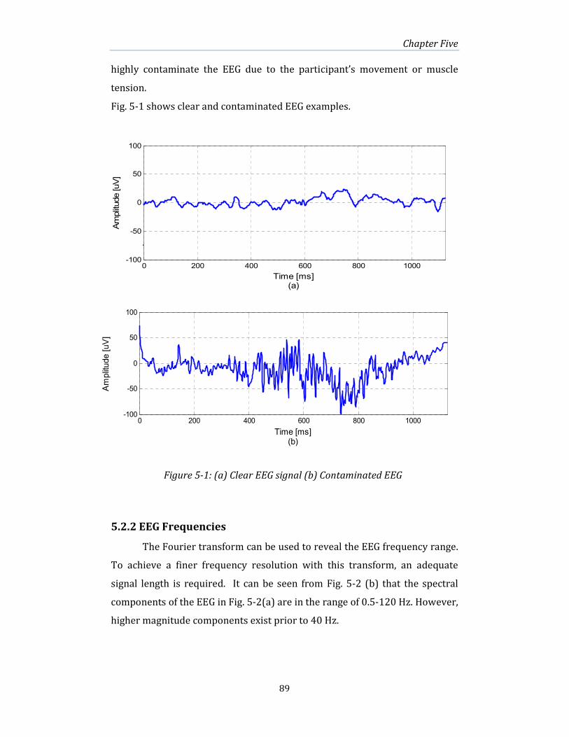
Chapter Five
89
highly contaminate the EEG due to the participant’s movement or muscle
tension.
Fig. 5-1 shows clear and contaminated EEG examples.
.
5.2.2 EEG Frequencies
The Fourier transform can be used to reveal the EEG frequency range.
To achieve a finer frequency resolution with this transform, an adequate
signal length is required. It can be seen from Fig. 5-2 (b) that the spectral
components of the EEG in Fig. 5-2(a) are in the range of 0.5-120 Hz. However,
higher magnitude components exist prior to 40 Hz.
Figure 5-1: (a) Clear EEG signal (b) Contaminated EEG
0 200 400 600 800 1000-100
-50
0
50
100
Time [ms](a)
Amplitude [uV]
0 200 400 600 800 1000-100
-50
0
50
100
Time [ms](b)
Amplitude [uV]

Chapter Five
90
0 200 400 600 800 1000 1200 1400 1600 1800 2000 2200-100
-50
0
50
100
Time [ms](a)
Amplitude [uV]
5.2.3 Noise Mitigation through Averaging
There are a number of noise sources that can contaminate the EEG
recording. Muscle activity (EMG), heart activity, environment electrical noise
and poor conductance between electrodes and the scalp have been
considered main reasons for the generated noise components in the EEG
[18]. The reduction of noise can be achieved by reducing the noise
component of the signal (such as signal averaging) or by inspecting the noisy
recordings, isolating and excluding them from analysis.
Averaging the EEG can be considered a valid method for mitigating the
effect of noise components and to extract the event-related (e.g. to a
stimulus) waveform from the background EEG. In other words, averaging
prepares the signal for the event-related potential (ERP) components
extraction [16]. An EEG signal with noise, y(i), can be considered as the sum
of the EEG itself, s(i), and the background noise signal, n(i) [19].
Figure 5-2: (a) an EEG epoch of 2200 ms. (b) The single sided spectral
component of the EEG in (a).
0 20 40 60 80 100 120 140 160 180 2000
1
2
3
4
5
6
Frequency [Hz](b)
|Y(f)|

Chapter Five
91
¨(6) = 5(6) + 7(6) (5-1)
The noise n(i) is assumed to be generated by random processes. The
application of signal averaging depends upon the following two conditions:
uncorrelated relationship between the EEG and background noise and the
absence of event-related variation in the time course of the EEG, i.e. the
occurrence of each salient waveform is always time-locked (see Fig. 5-4)[19].
Considering M as the number of epochs of an EEG, signal averaging
can be computed as
H©�ªH«�(6) = 1�� ª(6)�ª&V (5-2)
where yr is the time-locked EEG epoch and yaverage is the average of M number
of EEG epochs that have equal lengths. As mentioned, signal averaging is used
to extract the ERP components and mitigates the components of noise
included.
A useful measure for noise variability is the root-mean-square (RMS).
The RMS of noise (����) was defined as the mean deflection of the average
voltage of noise and for a series of m measurements [20]:
YªIG = ¬1Z�(Yª − Yª)RIª&V (5-3)
where �� is the base-to-peak voltage measure. In other words, it’s the
maximum excursion from the average voltage of noise ��. The reduction in
noise, as a consequence of EEG averaging, is described by the equation:
Y�ªIG = YªIG√� (5-4)
where���� is the noise before signal averaging and�����is the noise
following signal averaging. It’s clear from (5-4) that the noise is reduced by
the square root of the number of EEG epochs in the average.

Chapter Five
92
10 20 30 40 50 60 70 80 90 1000.1
0.2
0.3
0.4
0.5
0.6
0.7
0.8
0.9
1
No. of averaged trials
Re
pre
sen
tati
ve
qu
an
tity
of
no
ise
Fig. 5-3 shows an illustration to equation 5-4. For example, averaging
over 25 epochs reduces the noise to about 20% whereas averaging over 100
epochs reduces the noise to about 10% from the original magnitude. Fig. 5-4
(a1 & b1) shows the traces for a set of P300 measured from the electrodes Fz
and Cz, and for 38 oddball trials with a 1 second length epoch. The average of
these traces is given in Fig. 5-4 (a2 & b2). This figure clearly shows the
noticeable improvement in the averaged P300 trace peaking 400 ms from the
stimulus onset (0 ms). The stray variations of high frequency are clearly
mitigated.
Figure 5-3: The reduction in noise versus averaging over trials
5.3 Wavelet Analysis
The presented algorithms in Chapter 3 for CWT, WCS and WC were
applied in the current chapter to analyse the EEG and the ERP epochs. Monte
Carlo methods were used to estimate the statistical significance level of the
WC against the background spectrum [21].
5.3.1 Data Acquisition and Test Description
The EEG signals were recorded from a 32-electrode cap according to the
10/20 international system (see Fig. 2-7). EEG data was collected from 12
participants with an average age of 20.08±2.61; eight of them were males.
The Griffith University ethics number for human research was (PSY /92 /09
/HREC).
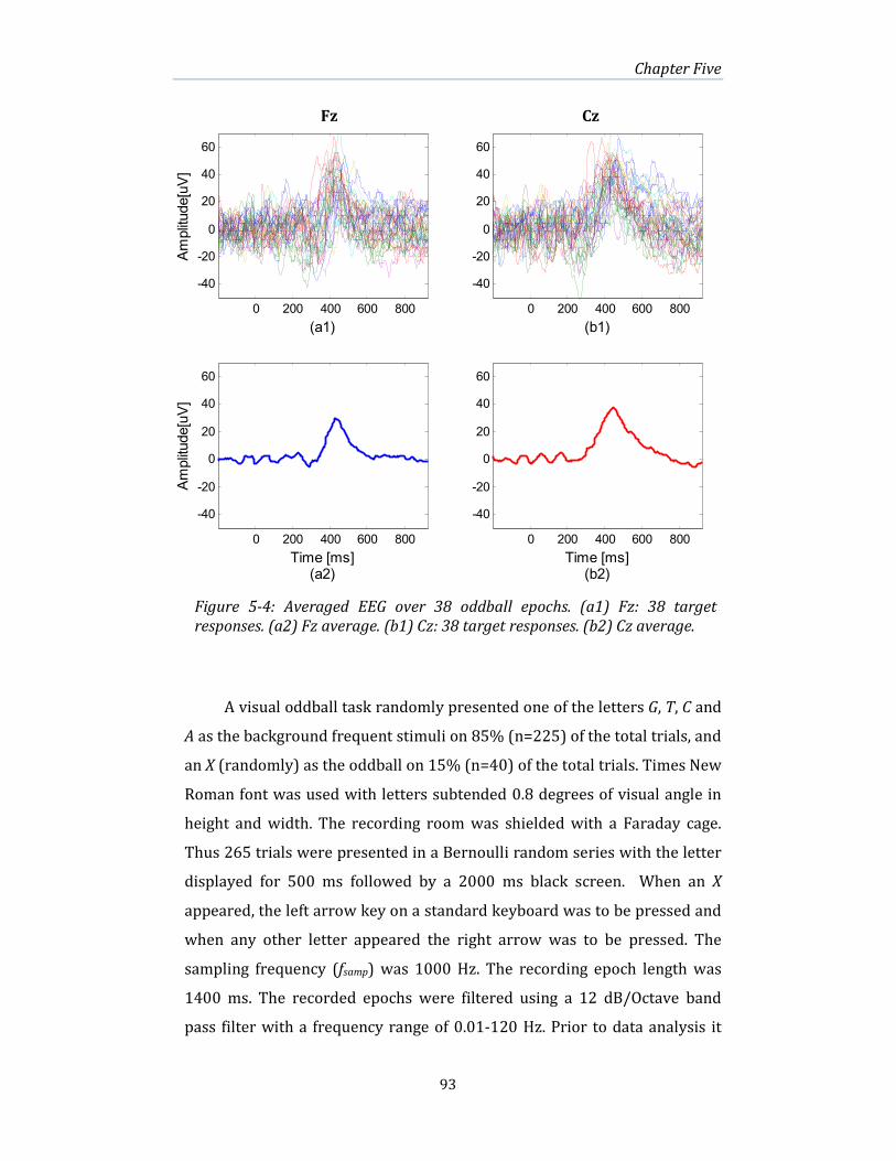
Chapter Five
93
A visual oddball task randomly presented one of the letters G, T, C and
A as the background frequent stimuli on 85% (n=225) of the total trials, and
an X (randomly) as the oddball on 15% (n=40) of the total trials. Times New
Roman font was used with letters subtended 0.8 degrees of visual angle in
height and width. The recording room was shielded with a Faraday cage.
Thus 265 trials were presented in a Bernoulli random series with the letter
displayed for 500 ms followed by a 2000 ms black screen. When an X
appeared, the left arrow key on a standard keyboard was to be pressed and
when any other letter appeared the right arrow was to be pressed. The
sampling frequency (fsamp) was 1000 Hz. The recording epoch length was
1400 ms. The recorded epochs were filtered using a 12 dB/Octave band
pass filter with a frequency range of 0.01-120 Hz. Prior to data analysis it
Figure 5-4: Averaged EEG over 38 oddball epochs. (a1) Fz: 38 target
responses. (a2) Fz average. (b1) Cz: 38 target responses. (b2) Cz average.
0 200 400 600 800
-40
-20
0
20
40
60
(a1)
Amplitude[uV]
0 200 400 600 800
-40
-20
0
20
40
60
(b1)
0 200 400 600 800
-40
-20
0
20
40
60
Time [ms](a2)
Amplitude[uV]
0 200 400 600 800
-40
-20
0
20
40
60
Time [ms](b2)
Fz Cz

Chapter Five
94
was important to visually inspect individual trials. Trials containing gross
movement artefacts and eye blink artefacts (voltage exceeding ±100 µV
within the epoch) were removed from further analysis. Removing
unaccepted trials typically resulted in retaining approximately 85-95% of
trials across participants. For each of the oddball and frequent trials, the
CWT and WCS were applied as they provide the basis for the WC algorithm
used in this chapter.
5.3.2.1 Results for CWT and WC analysis
The two time series shown in Fig. 5-5(a) demonstrate single trial examples
of a typical oddball as well as frequent trials from the same participant at the
Fz electrode. The CWT using the complex Morlet function was applied to the
two trials in Fig. 5-5(a) to give the wavelet scalogram maps for oddball and
frequent trials separately as shown in Fig. 5-5(b) & Fig. 5-5(c), respectively. It
is clear from Fig. 5-5(a) that a significant difference between oddball and
frequent trials occurred at 400 ms from the stimulus onset. Fig. 5-5 (b & c)
reveals how the wavelet coefficients are distributed along scales. The colour
bar reflects the amplitude of the wavelet coefficients. The red region refers to
the position and frequencies of the P300. It is evident that the large wavelet
coefficients for the oddball P300 occur in the higher range, at 125-300
(scales), which corresponds to low frequencies: 3.33-8 Hz. The frequent trial
has dispersed weak wavelet coefficients compared to the oddball trial (Fig. 5-
5 c).
The WCS (see section 3.2.4.3) clearly shows the scale and location of
the dominant features or local covariance between two EEG channels in the
time-scale plane. Fig. 5-6 (a & b) shows the WCS between Fz-Cz for the
oddball and frequent trials, respectively. In Fig. 5-6(a2), the WCS power
(equation (3-28) given by�[%��(5)�) was calculated for an oddball trial. The
P300 corresponds to large amplitude cross spectrum values between Fz and
Cz for the period 400-600 ms at high scales (180-300). The WCS in the
frequent trial (Fig. 5-6 b2) shows a very weak cross spectrum between Fz-Cz
as compared with Fig. 5-6 (a2). However, wavelet coherence can be used to
find similarities between EEG epochs when the common power is low [21].

Chapter Five
95
-200 0 200 400 600 800 1000 1200-40
-20
0
20
40
60
Time [ms]
(a)
Amplitude [uV]
frequent
oddball
Figure 5-5: (a) The measured Fz channels during single oddball and frequent
trials. (b) and (c) The computed CWT coefficients for oddball and for frequent
trials. The colour bar was fixed on a maximal value of 100 in both (b) and (c)
for fair comparison. The higher scales refer to lower frequencies.
(a)
(b)
(c)

Chapter Five
96
0 200 400 600 800 1000 1200
-20
0
20
40
Time [ms]
(a1)
Amplitude [uV]
1
oddball Fz
oddball Cz
0 200 400 600 800 1000 1200
-20
0
20
40
Time [ms]
(b1)
Amplitude [uV]
1
Frequent Fz
Frequent Cz
Figure 5-6: The wavelet cross spectrum (WCS) in oddball and frequent trials
(a1) Fz (red) and Cz (dashed-blue) signals in an oddball trial. (a2) The WCS
between Fz-Cz in (a1). (b1) Fz (red) and Cz (dashed-blue) signals in a
frequent trial. (b2) The WCS between Fz-Cz in (b1).

Chapter Five
97
When applying wavelet coherence between Fz-Cz channels in both
types of trials, some differences were noticed in the patterns especially in the
delta band where high coherence was seen in the oddball contours but no
such coherence existed in the frequent trials for the same band (see Fig. 5-7).
The y-axis represents the frequencies of interest, from which the EEG bands
can be extracted. The coherence in the gamma band is difficult to see in this
representation and required a different approach, as discussed below.
Each wavelet coherence trial image (-200 to 1200 ms) was averaged
across trials for each condition (oddball vs. frequent) separately and then
averaged across time in order to produce the averaged wavelet coherence for
each participant at each frequency. The average wavelet coherence for
oddball and frequent conditions for one participant is shown in Fig. 5-8 (a).
The mean difference in averaged coherence (across the 12 participants)
between the oddball and frequent trials is shown according to the EEG bands
in Fig. 5-8 (b).
For the final averaging process, the group mean and standard error of
the mean for each frequency band were used to provide the results in
standardized normal form (Z scores) for the group analysis of wavelet
coherence between Fz-Cz as shown in Fig. 5-8(c). In this figure, a significant
difference at Zlow-freq= 4.6292 (P=0.00006) and Zgamma= 3.273 (P =0.00106)
can be seen. This is apparent in the low frequency band and in the gamma
band.
Time[ms]
0 200 400 600 800 1000 1200
2
3
7
15
30
60
120
0.1
0.2
0.3
0.4
0.5
0.6
0.7
0.8
0.9
Time[ms]
Frequency[Hz]
0 200 400 600 800 1000 1200
2
3
7
15
30
60
120
Figure 5-7: (Left contour) WC between Fz-Cz in an oddball trial. (Right
contour) WC between Fz-Cz in a frequent trial. The colour scale refers to
the magnitude of coherence in the time-frequency plane.
Oddball Frequent
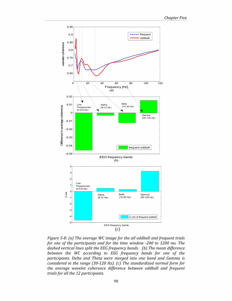
Chapter Five
98
(c)
-5
-4
-3
-2
-1
0
1
2
3
4
Z unit
EEG frequency bands
(c)
Z unit of frequent-oddball
Gamma
(30-120 Hz)Alpha
(8-12 Hz)
Low
Frequencies
(0.5-8 Hz)
Beta
(12-30 Hz)
Figure 5-8: (a) The average WC image for the all oddball and frequent trials
for one of the participants and for the time window -200 to 1200 ms. The
dashed vertical lines split the EEG frequency bands. (b) The mean difference
between the WC according to EEG frequency bands for one of the
participants. Delta and Theta were merged into one band and Gamma is
considered in the range (30-120 Hz). (c) The standardized normal form for
the average wavelet coherence difference between oddball and frequent
trials for all the 12 participants.
0 20 40 60 80 100 120
0.65
0.7
0.75
0.8
0.85
0.9
0.95
Frequency [Hz](a)
wavelet coherence
frequent
oddball
-0.05
-0.04
-0.03
-0.02
-0.01
0
0.01
0.02
Difference in average coherence
EEG frequency bands(b)
frequent-oddball
Gamma
(30-120 Hz)
Beta
(12-30 Hz)Low
Frequencies
(0.5-8 Hz)
Alpha
(8-12 Hz)
Chapter Five
99
5.3.2.2 Results for Gamma Correlation
During the oddball task, an oddball trial is often followed by several
frequent trials before the next oddball trial. When responding to these
frequent trials, expectancy should grow as more of them occur in sequence.
This cognitive process may alter the coherence in the EEG channels.
Since the ratio of frequent to oddball trials was approximately six,
oddball trials followed by at least six frequent trials were compiled for
analysis. From each participant, eight such oddball trials were taken with the
six subsequent frequent trials after each oddball according to the matrix
shown in Fig. 5-9(a).
Wavelet coherence was computed between Fz-Cz for the above set of
frequent trials. To reveal only the highly significant parts of the wavelet
coherence, a threshold (as in [21]-[22]) was applied on each of the wavelet
coherence coefficients as Fig. 5-9(b) shows. The applied threshold24 varied
with scale such that the threshold spanned 0.68 <Th< 0.84. These thresholds
were used for significance level estimation of the wavelet coherence at each
wavelet scale, such that if any value in the contour at a specific time and scale
>= threshold, it remains in the resultant contour, otherwise it is equal to zero.
Figure 5-10 shows the grand averaged time series including all the 12
participants. These waveforms have a P300 oddball response evident in the
period 350-600ms. It was of interest to examine portions of the epoch for
differences in gamma coherence. Hence, the epoch was divided into four
periods (in ms): -200-0 ms is the pre-stimulus period, 0-350 ms is a pre-P300
processing period, 350-600 ms spans the P300 period, and
600-900 ms is the post P300 period. Fig. 5-9(b) shows the selection of the
350-600 ms time window (a duration of 250 ms) from the gamma coherence
scalogram.
24 The thresholds were spanned between 0.68 and 0.84 according to each of the wavelet
scales used and also depending on the significance level of the colour scale in the
coherogram which, in turn, depends on the two input EEG signals.

Chapter Five
100
F
F
F
F
F
F
F
F
F
F
F
F
F
F
F
F
F
F
F
F
F
F
F
F
F
F
F
F
F
F
F
F
F
F
F
F
F
F
F
F
F
F
F
F
F
F
F
F
О
О
О
О
О
О
О
О
Consecutive trials after oddball event
1
2
3
4
5
6
7
8
Frequent
trial
Gamma band 30-120 Hz
F
Wavelet coherence
Apply threshold
Window selection between 350-600 ms
in the Gamma band.
Time[ms]
Frequency[Hz]
0 200 400 600 800 1000 1200
2
3
7
15
30
60
120
250
500Time[ms]
Frequency[Hz]
0 200 400 600 800 1000 1200
2
3
7
15
30
60
120
250
500
400 450 500 550 600
Figure 5-9: (a) A matrix of selected oddballs (rows) with six subsequent frequent
trials (columns) after each oddball. The ‘O’ inside the square refers to the
oddballs whereas the letter ‘F’ refers to the frequent trials following the oddball
event. The arrow refers to the increasing trial number from the oddballs. (b) The
wavelet coherence before and after threshold and the chosen Gamma window
for analysis in the time duration (350-600 ms) and frequency range (30-120
Hz). The selection of this window was based on a visual inspection of the time
series in Fig. 5-10.
(a)
(b)
Od
db
all
#

Chapter Five
101
The next step was averaging the wavelet coherence in the selected
windows in both the time direction and frequency direction (30-120 Hz) to
produce a single value representing the average coherence of the trial. When
this process was completed for the whole matrix (Fig. 5-9 a), the resultant
values were averaged vertically across the eight oddball trials for each of the
six following frequent trials as seen in Fig. 5-9(a). As a result, six values were
produced from the average across the 12 participants. This procedure was
repeated for the four selected time windows. The correlation between these
gamma values and the trial position (post oddball) was computed. Fig. 5-11
(a, b, c and d) shows each of these correlations for the four time periods and
also reveals gamma coherence changes with the increased trial number from
the oddball trial. Fig. 5-11 (a) shows the pre-stimulus period (-200-0 ms)
which has a correlation coefficient of R2 = 0.1064. Fig. 5-11 (b) shows the
P300 pre-processing period (0-350 ms) with a correlation coefficient of R2 =
0.452. Fig. 5-11 (c) shows the P300 period (350-600 ms) with a correlation
coefficient of R2 = 0.935, P = 0.0015. Finally Fig. 5-11 (d) shows the post-
-200 0 200 400 600 800 1000 1200-30
-20
-10
0
10
20
30
Amplitude [uV]
Oddball
Fz
-200 0 200 400 600 800 1000 1200-30
-20
-10
0
10
20
30Cz
Time [ms]
(a)
Amplitude [uV]
-200 0 200 400 600 800 1000 1200-30
-20
-10
0
10
20
30
Frequent
Fz
Amplitude [uV]
-200 0 200 400 600 800 1000 1200-30
-20
-10
0
10
20
30Cz
Time [ms]
(b)
Amplitude [uV]
Figure 5-10: (a) The grand average of the oddball trials at Fz and Cz electrodes
for 12 participants (a total number of 424 oddballs was averaged). (b) The same
averaging process for the frequent trials (a total number of 2556 frequents were
averaged).

Chapter Five
102
response period (600-900 ms) with a correlation coefficient of R2 = 0.1861.
Only Fig. 5-11(c) is significant using the SPSS package to test the significance
of the Pearson correlation coefficient. The pre-stimulus period will have low
correlation since the stimulus has not been presented yet. The pre-
processing (Pre-P300) period has a higher gamma correlation than the pre-
stimulus period since the stimulus has been presented and is being processed
requiring increasing activity between the frontal and temporal/parietal
areas. The P300 period has a higher gamma correlation than the preceding
periods due to the actual response requiring greater communication between
the frontal and temporal/parietal areas. The post-response (Post-P300)
period shows a decline in gamma correlation. This is as expected since there
will not be any need for further processing well after the stimulus has
occurred and its identity established, so the system continues to relax back to
its pre-stimulus state.
The high correlation value obtained in Fig. 5-11 (c) was also tested for
significance by using the Bootstrap method [23]. This method selects data
from a random sample of eight subjects out of the pool of 12 subjects
(without replacement) as the data set. The correlation was then performed
on this data set. This process was repeated 25000 times and the histogram of
the correlation values is plotted in Fig. 5-12. It is apparent that the
correlations for the 25000 iterations occur mainly in the range 0.85-0.95.
This indicates that the high correlation from this test is robust over sampling
for different participants.

Chapter Five
103
0.39
0.395
0.4
0.405
0.41
0.415
0.42
0.425
0.43
0 1 2 3 4 5 6
Aver
ag
e G
am
ma
co
here
nce
Distance from oddball trial in single trial per step
the period -200-0 ms
R2 = 0.1064
0.44
0.45
0.46
0.47
0.48
0.49
0.5
0 1 2 3 4 5 6
Aver
ag
e G
am
ma
co
here
nce
Distance from oddball trial in single trial per step
the period 0-350 ms
R2 = 0.452
0.48
0.485
0.49
0.495
0.5
0.505
0.51
0.515
0 1 2 3 4 5 6
Aver
ag
e G
am
ma c
oh
ere
nce
Distance from oddball trial in single trial per step
the period 350-600 ms
R2 = 0.9352
0.47
0.475
0.48
0.485
0.49
0.495
0.5
0.505
0 1 2 3 4 5 6
Aver
age G
am
ma
co
her
en
ce
Distance from oddball trial in single trial per step
the period 600-900 ms
R2 = 0.1861
Figure 5-11: The plots show the group averaged Gamma coherence for
frequent trials at each of the trial positions after the last oddball and for the
time periods: (a) -200-0 ms, (b) 0-350 ms, (c) 350-600 ms, (d) 600-900 ms.
These groups of frequent trials were depicted in Fig. 5-9 (a).
(a)
(b)
(c)
(d)
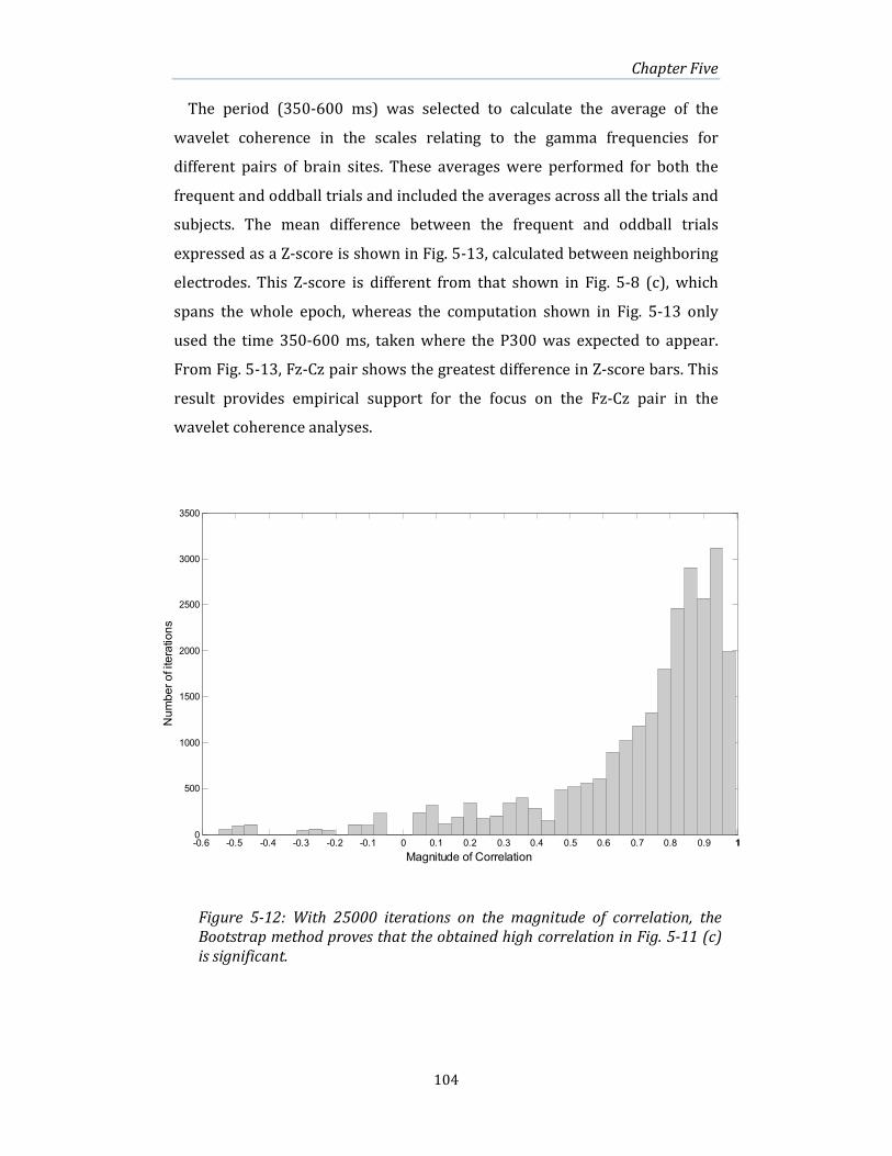
Chapter Five
104
The period (350-600 ms) was selected to calculate the average of the
wavelet coherence in the scales relating to the gamma frequencies for
different pairs of brain sites. These averages were performed for both the
frequent and oddball trials and included the averages across all the trials and
subjects. The mean difference between the frequent and oddball trials
expressed as a Z-score is shown in Fig. 5-13, calculated between neighboring
electrodes. This Z-score is different from that shown in Fig. 5-8 (c), which
spans the whole epoch, whereas the computation shown in Fig. 5-13 only
used the time 350-600 ms, taken where the P300 was expected to appear.
From Fig. 5-13, Fz-Cz pair shows the greatest difference in Z-score bars. This
result provides empirical support for the focus on the Fz-Cz pair in the
wavelet coherence analyses.
-0.6 -0.5 -0.4 -0.3 -0.2 -0.1 0 0.1 0.2 0.3 0.4 0.5 0.6 0.7 0.8 0.9 110
500
1000
1500
2000
2500
3000
3500
Magnitude of Correlation
Number of iterations
Figure 5-12: With 25000 iterations on the magnitude of correlation, the
Bootstrap method proves that the obtained high correlation in Fig. 5-11 (c)
is significant.

Chapter Five
105
-2
-1
0
1
2
3
4
5
Electrode pairs
Z score amplitude
Pz-Cz
C3-C4 Fz-PzC4-Cz
P3-P4
F3-F4
C3-Cz
F4-CzF3-Cz Fz-Cz
C3-F3Pz-P3
C3-P3
Pz-P4
F3-Fz F4-Fz F4-C4 C4-P4
P4-Cz
P3-Cz
5.4 Discussion of Results
This chapter aimed at showing the utility of wavelet coherence analysis:
(a) for identifying more clearly individual trial features that are not easily
detected in the raw time series; (b) for averaging in the wavelet domain to
test for coherence between electrode sites that relate to the cognitive
processes involved in oddball monitoring; and (c) providing possible
evidence for brief activation of a fronto-central circuit. Each of the sections
below addresses one of these areas.
The results of this chapter underline the potential utility of wavelet
coherence analysis for providing lucid visual representation of important
features that may be less evident in the simple time series. Visual oddball
tasks can reveal striking differences in single trials between oddball and
frequent stimuli as shown in Figs 5-5, 5-6 and 5-7. These figures provide a
descriptive view of the increased resolution of features in the wavelet
coherence domain as compared to viewing the individual electrodes in the
Figure 5-13: The Z-score bar for the difference between frequent and oddball trials
in the Gamma section represented by the wavelet coherence as in Fig. 5-8 (c) except
that the considered time window is in the range 350-600 ms. The graph shows the
highest difference between the electrode pair Fz-Cz.
Chapter Five
106
time domain. Moreover, they demonstrate the way that this facilitates
comparisons across experimental conditions. For example, concerning
oddball trials, there is considerably more coherence in the lower frequencies.
The grand averaged analysis of the wavelet coherence provided the mean
difference between oddball and frequent stimuli in standardized normal
form (Z scores, Fig. 5-8 c). A significant difference was found in the low
frequency band (Delta-Theta), where wavelet coherence is higher in the
oddball trials than in the frequent trials. This corresponds to the emergence
of the P300 component and it confirms the results of [24] which used the
discrete wavelet transform (DWT) to show that simple wavelet
decomposition can identify the frequency band of a P300 response.
In contrast, in the gamma band (Fig. 5-8 c), the frequent trials produce
higher average wavelet coherence. This result agrees with [15] and may
reflect either continued expectation of the oddball or maintenance of the
memory trace that matches the frequent stimulus event [2]. These gamma
results with a visual oddball task differ from those of [25], [26] who used an
auditory oddball (with counting or reading) processed with the DWT. They
found a number of very short latency phase-locked gamma activations. It is
likely that the modality and peripheral tasks need to be taken into account in
interpreting gamma coherence during an oddball task. The expectancy
hypothesis25 was supported by further analyses taking into account the post-
oddball trial position of a series of frequent trials (Figs. 5-9 and 5-11). A very
high correlation was observed between the post-oddball position and gamma
coherence amplitude during the P300 processing period (350 – 600 ms). This
might correspond to a form of expectation of context switch that, the longer
the series of frequent trials extends, the greater it becomes. These two
possible explanations of the gamma activity (memory trace maintenance or
oddball expectation) could be further pursued by using the three-stimulus
oddball wherein a rare irrelevant distracter (or deviant) is added to the task,
25 The expectancy hypothesis is an explanation for the P300 across the trials where the
increased number of frequent trials expectancy builds the longer the sequence of frequent
trials. This produces more gamma frequencies in the P300 time region, especially as
expectancy builds, and it may set up a communication link between frontal and central areas.
Chapter Five
107
with task instructions that only require a response to oddball stimuli (no key
is pressed to non-oddball stimuli). The “maintain context” hypothesis would
be supported if the distracter had no impact on the coherence correlation
since the context of ‘no response’ is to be maintained. However, if there was a
change in gamma coherence to the rare occurrence of the distracter stimulus,
this would support gamma-related expectancy tracking. Furthermore, future
research on this topic could extend the expectation with artificially long runs
of frequent trials (12-15 trials) and determine whether the correlation is
maintained beyond the relatively modest six trials in the present experiment.
There are some other considerations. In Fig. 5-13, the difference in gamma
coherence between oddball and frequent stimuli shows a maximal difference
for the Fz-Cz pair. Although the spatial distance between Cz and Pz is similar,
there was only a small gamma coherence difference for the pairs even though
the P300 is large at all of Fz, Cz and Pz. Thus large P300 at adjacent electrode
sites is insufficient to yield a large gamma coherence difference. This
provides some support for a spatial coupling between Fz and Cz during an
oddball task in the 350-600 ms time window, wherein gamma coherence
may reflect a monitoring process for an expected event (the oddball) and
appears to be greatest after a sequence of non-occurrences (i.e., during a
sequence of frequent background trials). Once the oddball occurs, the frontal-
central linkage is attenuated (gamma coherence declines) and the process
begins again for the next sequence. This specificity in frontal-central
coherence for oddball processing has not been previously reported. A
possible limiting factor could be that part of the coherence seen in
neighbouring electrodes for the delta-theta range is due to simple proximity.
Future work could aim at validating the present results, which are based on
surface sensor (electrode) sources with computed dipole source coherence.
This might be best achieved with a higher density of electrodes than that
which was available here, such as in a 128–channel system.
Finally, practical extension is planned for computing the electrode pair
coherence in real time and making it available for feedback to the participant
during the task. This could permit the study to have value as an attention
Chapter Five
108
training aid, for example by displaying the gamma coherence and relating
this to oddball detection speed and accuracy especially in more challenging
variations of the simple oddball task than the one used here. However, since
the CWT and WC are computationally intensive processes, the next chapters
present a novel FPGA implementation to these algorithms.
5.5 Summary
This chapter has presented a novel application of WC to the EEG
waveforms recorded in a visual oddball test. Extracting features from
different EEG trials were applied using the CWT and the local covariance
between two EEG signals from different brain sites was obtained by the WCS
in the time-scale plane. When the common power of the EEGs is low, the WC
was used instead of the WCS. The undertaken WC analysis provided possible
evidence for the brief activation of a fronto-central circuit and signified the
EEG frequencies of high coherence through averaging. The entire trials of the
visual test were analyzed and interpreted in one comprehensive scheme. The
obtained results of the average wavelet coherence have shown significant
differences between oddball and frequent trials in the low frequency bands
and in the gamma band where evidence was garnered for the expectancy
hypothesis. The expectancy hypothesis was examined by the post-oddball
trial position of a series of frequent trials and showed a very high correlation
between the post-oddball position and gamma coherence amplitude during
the P300 processing period (350-600ms). This adds further support to the
expectancy hypothesis. The relation of gamma band to cognition has been
discussed and compared with other state of the art methods.
Chapter Five
109
5.6 References
1 Y. T. Qassim, T. R. Cutmore, D. A. James, and D. D. Rowlands, "Wavelet
coherence of EEG signals for a visual oddball task," Computers in Biology
and Medicine, vol. 43, pp. 23-31, 2013.
2 J. Polich, “Updating P300: an integrative theory of P3a and P3b,” Clinical
Neurophysiology, vol. 118, pp. 2128-2148, 2007.
3 M. Senderecka, et al., “Event-related potentials in children with attention
deficit hyperactivity disorder: An investigation using an auditory oddball
task”, International Journal of Psychophysiology. (2011),
doi:10.1016/j.ijpsycho.2011.05.006.
4 G. McCarthy, et al., “Infrequent events transiently activate human pre-frontal and parietal cortex as measured by functional MRI”, Journal of
Neurophysiology, 77, pp. 1630-1634, 1997.
5 E. Kirino, et al., “Prefrontal activation evoked by infrequent target and
novel stimuli in a visual target detection task: An event-related functional
magnetic resonance imaging study,” Journal of Neuroscience, 20 (17), pp.
6612–6618, 2000.
6 S. A. Huettel and G. McCarthy, “What is odd in the oddball task?: Prefrontal
cortex is activated by dynamic changes in response strategy,”
Neuropsychologia, vol. 42, pp. 379-386, 2004.
7 E. K. Miller & J. D. Cohen, “An integrative theory of prefrontal cortex
function”, Annual Review of Neuroscience, 24, pp. 167–202, 2001.
8 D. E. J. Linden, “The P300: where in the brain is it produced and what does
it tell us?”, The Neuroscientist, vol. 11, pp. 563- 576, 2005.
9 T. Medkour, et al., “Graphical modelling for brain connectivity via partial
coherence,” Journal of Neuroscience Methods, vol. 180, Issue 2, pp. 374-383,
2009.
10 R. Srinivasan, et al., “EEG and MEG coherence: Measures of functional connectivity at distinct spatial scales of neocortical dynamics,” Journal of
Neuroscience Methods, vol. 166, Issue 1, 15 October 2007, pp. 41-52.
11 J.-P. Lachaux, et al., “Estimating the time-course of coherence between single-trial brain signals: an introduction to wavelet coherence,”
NeurophysiolClin, vol. 32, pp. 157-174, 2002.
12 J. Jung and T. Kobayashi, “Induced gamma-band activity in a similarity
grouping task,” International Congress Series, vol. 1270, pp. 225-228, 2004.
Chapter Five
110
13 A. W. Keizer, R. Verment and B. Hommel, “Enhancing cognitive control through neurofeedback: A role of gamma-band activity in managing
episodic retrieval,” Neuroimage, vol. 49, pp. 3404-3413, 2010.
14 L. Marshall, M. Molle, P. Bartsch, “Event-related gamma band activity during
passive and active oddball tasks,” NeuroReport, vol. 7, p. 1517, 1996.
15 O. Bertrand, C. Tallon-Baudry, M. H. Giard and J. Pernier, “Auditory induced
40-Hz activity during a frequency discrimination task,” NeuroImage 7: S370
(1998).
16 A. Mouraux and G. Iannetti, “Across-trial averaging of event-related EEG
responses and beyond,” Magnetic Resonance Imaging, vol. 26, pp. 1041-1054,
2008.
17 C. Tallon-Baudry and O. Bertrand, “Oscillatory gamma activity in humans
and its role in object representation,” Trends CognSci, vol. 3, pp. 151-162,
1999.
18 M. Teplan, "Fundamentals of EEG measurement," Measurement Science
Review, vol. 2, 2002.
19 J. Dempster, “The Laboratory Computer: A practical guide for Physiologists
and Neuroscientists”, Academic Press, London, 2001.
20 T. R. Cutmore and D. A. James, "Identifying and reducing noise in
psychophysiological recordings," International Journal of Psychophysiology,
vol. 32, pp. 129-150, 1999.
21 A. Grinsted, J. C. Moore and S. Jevrejeva, “Application of the cross wavelet
transform and wavelet coherence to geophysical time series,” Nonlinear
Processes in Geophysics, pp. 561-566, 2004.
22 A. Grinsted, J. C. Moore and S. Jevrejeva. “Cross Wavelet and Wavelet Coherence,” Matlab Package. Available:
http://www.pol.ac.uk/home/research/waveletcoherence/ Accessed August
22, 2012.
23 P. Hall, “The bootstrap and Edgeworth expansion”, Springer Verlag, (1997).
24 T. Demiralp, A. Ademoglu, M. Schürmann, C. Basar-Eroglu, and E. Basar,
“Detection of P300 waves in single trials by the wavelet transform (WT),”
Brain and Language, vol. 66, pp. 108-128, 1999.
25 I. Gurtubay, M. Alegre, A. Labarga, A. Malanda, J. Iriarte, and J. Artieda, “Gamma band activity in an auditory oddball paradigm studied with the wavelet
transform,” Clinical Neurophysiology, vol. 112, pp. 1219-1228, 2001.
26 I. Gurtubay, M. Alegre, A. Labarga, A. Malanda, and J. Artieda, “Gamma band responses to target and non-target auditory stimuli in humans,”
Neuroscience Letters, vol. 367, pp. 6-9, 2004.

Chapter Six
111
Chapter 6 FPGA Implementation and Design
Optimization of a Morlet CWT for
EEG Analysis
This chapter presents the design and implementation of a Morlet CWT
engine for EEG analysis using an FPGA. A comprehensive description of the
design details including FPGA implementation with design optimizations in
area and speed, timing analysis, synthesis and verification of results are
provided. The optimizations used here aided in adapting the design to the
available FPGA memory in order to analyse another EEG signal following the
first EEG and produce their CWTs. The generated CWTs constitute the basis
for the wavelet coherence design and analysis in the next chapter.
This chapter is closely based on two blind peer reviewed published
research conference papers [1]-[2], one abstract presented at a conference
and one paper submitted to a journal. The chapter begins with a discussion of
the method for CWT implementation on VLSI. System requirements are then
presented and the required VHDL controllers to operate the design are
highlighted. Several methods to test and verify the results are provided and
the performed optimizations in algorithm simplification, FPGA memory and
operational frequency are demonstrated.

Chapter Six
112
6.1 Related Work
Owing to the nature of the heavy computations implied in the CWT
algorithm, few works in the literature are available targeting the VLSI of the
CWT. The architectures of implementing the CWT convolver in a VLSI design
was investigated in [3] and various realizations were presented, although
they all depend on the operation of convolution which is well known as a
complex and slow operation. In [4] a dedicated DSP processor was employed
for implementing the B-spline wavelet for detecting singularities in
electromyogram (EMG) interference patterns. This achieved an execution
time of 47.9 ms for a 1024 point signal. In [5] a General Purpose processor
(GPP) was used to implement the CWT for feature extraction of event related
potential (ERP) using the Mexican hat wavelet. This achieved a run time of up
to 10 ms. In [6] and [7], however, they employed multiple Virtex FPGA
devices (Virtex II XC2V500 and Virtex II pro XC2V30P respectively) for the
lifting scheme JPEG filters in the first FPGA and FIR filters for target motion
estimation in the second FPGA. These previous works in the field either
depend on the slow convolution operation such as [3], [7] or using a
processor [4]-[5] (these employed the recursive algorithm and the t-statistic
CWT method respectively) or using high end FPGA devices [6]-[7] (these
adapted the lifting scheme and convolution algorithms respectively).
This work presents a novel, generalized, configurable and low cost
FPGA platform for a CWT engine with a high throughput and a reduced
silicon area.
6.2 System Model
The implementation of the CWT is outlined in section 3.2.2.2 where
the presented CWT algorithm in (3-19) is modified to (3-23). This showed an
efficient method to calculate the wavelet coefficients in Fourier space and for
feasible implementation in the digital world, the FPGA. Equation (3-23) is
subject to optimizations in the digital hardware (presented later in this
chapter). These optimizations were required to alleviate the implied
complexity in the design since the optimum resource requirements and the
efficiency of system performance are the major indices towards an FPGA-

Chapter Six
113
based solution [8]. The CWT design engine, with the optimizations made was
performed within the Altium Designer environment.
6.2.1 FFT Based CWT
As presented in section 3.2.2.2, the computation of the CWT
coefficients is performed in Fourier space to avoid the complex convolution
operations at each wavelet scale within the CWT algorithm in (3-19). The
change from convolution into multiplication can be achieved with the Fourier
property in (3-7). The condition for performing the required multiplications
between the EEG signal and the wavelet function at each wavelet scale is
transforming both signals from the time domain into the frequency domain
representation as depicted in Fig. 3-4 and detailed in Fig. 6-1. In this figure
(Fig. 6-1), the input signal and the wavelet function are converted to the
frequency domain and saved in the buffers26 G1(⍵) and G2(⍵) prior to the
multiplication process (block B). The multiplications are performed between
G1(⍵) and G2(⍵) and the product is stored in a buffer. After that, the IFFT is
applied to return the product of multiplication to the time domain, which
represents the CWT coefficients.
The wavelet coefficients are calculated in a scale-based system, i.e.
the IFFT is performed several times and a vector of wavelet coefficients is
produced at one scale each time. Therefore, the IFFT is performed for each
wavelet scale. Once a vector of CWT coefficients is completed in a buffer, it is
shifted to the external RAM (SRAM IC) outside the FPGA due to the BRAM
size limitation. This process is repeated for each wavelet scale. The produced
wavelet coefficients at all scales are used to construct the CWT scalogram.
The flow diagram in Fig. 6-1 represents the implemented architecture
on the FPGA with some difference to the details listed in Fig. 3-4. The change
was made to block A in the figure by transforming the wavelet function to the
frequency domain at all scales before starting the multiplications. This means
the multiplication is continuously performed between the EEG signal and the
wavelet function through all the scales at once, whereas in Fig. 3-4 the
transform and multiplication are based on individual scales until obtaining
26 The buffer is the block RAM (BRAM) within the FPGA device.

Chapter Six
114
the wavelet coefficients at that scale. The operations are then repeated for
the next wavelet scale.
Figure 6-1: Flow chart for the digital implementation of the FFT based CWT
(based upon equation 3-23). BRAM is used as buffer; SRAM ICs are used for
final storage. A & B are the optimized blocks in the design.
Store samples
in buffer
G2())
G2()) G1())
g1(t)
Buffer containing
the EEG signal of 2n samples g1(t)
Store wavelet coefficients in buffer
at scale s, CWT(s)
Inverse FFT
FFT
Store samples
in buffer
G1())
Store product in buffer
G1()) × G2())
g2(t)
Buffer containing the
wavelet function g2(t) of
2n sampls at all scales s
FFT
B
Shift CWT coefficients
to SRAM ICs
FPGA
A
Chapter Six
115
6.2.2 The Wavelet Function Representation
In order to calculate the CWT, a representation of the base function in the
frequency domain is required. The wavelet function has a formula in the time
domain that differs from its counterpart in the frequency domain. Some of
the most commonly used non-orthogonal wavelet functions in CWT analysis,
that satisfy the admissibility criteria, are the Morlet, the Paul and the Mexican
hat. Table 6-1 shows the formula of these three wavelet functions in both the
time and frequency domains [9]:
Table 6-1: Three different wavelet bases in two domains
Function Time domain (t) Frequency domain (() Morlet +'V/w��!y#�'#^/R +'V/wx())�'(G!'!y)^/R Paul
2I6IZ!¯+(2Z)! (1 − 6�)'(I\V) 2I¯Z(2Z − 1)! x())(5))I�'G! Mexican
hat
(−1)I\V°� ]Z + VR_
?I?�I (�'t^) 6I°� ]Z + VR_ (5⍵)I�'(G!)^/R
Where:
H(() is the Heaviside step function (for Morlet and Paul), H(()= 1 if (>0,
H(()= 0 elsewhere.
(0 is the non-dimensional (central) frequency.
s is the scale and π-1/4 is the normalization factor.
m is order (for Paul), m is derivative of a Gaussian (for Mexican hat).
± stands for the gamma function.
The involvement of any of the wavelet functions of Table 6-1 in the CWT
design requires implementing block A and block B in Fig. 6-1 using one of the
following three possible options:
1. Calculate the wavelet function in the time domain at different
scales, apply the FFT to transform both the wavelet function and the
input signal into the frequency domain, then start multiplications
with the signal to be analyzed.
2. Directly calculate the wavelet function in the frequency domain at
different scales, then apply the FFT on the input signal and perform
the multiplications between the frequency domain wavelet function

Chapter Six
116
and the input signal.
3. Store the pre-calculated frequency domain-wavelet function points
in a lookup table (LUT). In this case, once the length of the input
signal and its sampling period are known, the points of the wavelet
function can be calculated only once off the device (prior to use) and
then downloaded into memory to be ready for multiplications that
follow the FFT on the input signal.
Methods 1 and 2 to calculate the CWT are structurally complex and
implementing them in hardware is not easy. They include trigonometric
functions, square root, power or factorials in the wavelet function in both
domains (Table 6-1), which requires significant FPGA resources besides
adding further computations that increase the run time. In addition, they
require design and synthesis for each new wavelet basis function. The LUT
option for implementing block A was selected because it avoids all the above-
mentioned complexities in methods 1 and 2 where no transform operations
or wavelet function calculations are required i.e. it provides an optimization
on blocks A and B of Fig. 6-1.
6.2.3 Wavelet Function Based Optimization
Despite the extensive reduction in calculations to perform the CWT by
using the FFT-IFFT method, the required silicon area for the design is still
considerably large. The LUT used to store the wavelet function in the
frequency domain is a perfect candidate for optimizing the design since it
speeds the calculations and reduces the design area. Therefore, it was chosen
in the CWT design. This is explained in the following sections.
6.2.3.1 Lookup Table (LUT)
The points of the wavelet function are pre-calculated in the frequency
domain and are downloaded to a LUT (G2(⍵)). The wavelet function in G2(⍵)
only needs to be reloaded when the required wavelet base function needs to
be changed. Hence, the implementation of block (A) in Fig. 6-1 can be
removed with its required VHDL code for operation and signal control and
replaced with a LUT G2(⍵) that contains easily readable points. This
approach makes the design versatile since it can be applied to many types of

Chapter Six
117
wavelet functions.
6.2.3.2 Zeros Exclusion
The transform of the wavelet function into the frequency domain allows
for another advantage which involves reducing further the number of
multiplication operations and the reduction of required storage. This
advantage can be seen by examining the shape of the wavelet basis function
in the frequency domain at different scales. The new shape of the wavelet
function contains a large number of zeros especially at higher scales. These
zeros represent a considerable portion of the points of the wavelet function
at each scale. For example, Fig. 6-2 shows the Morlet wavelet in the
frequency domain at (a) scale 10 and (b) scale 20. In both sub-figures it can
be noticed that zeros represent a considerable part of each vector of 1024
points. The start and end indexes and locations differ in each sub-figure.
These zeros can therefore be excluded from the LUT with only the non-zero
points being considered. This has a significant benefit in saving area in the
LUT as well as multiplication operations when mapped into VLSI design
(detailed in section 6.2.4.1). Although Fig. 6-2 is for the Morlet, the same
approach does apply for the other wavelet functions given in Table 6-1.
However, this method is not beneficial in calculating the CWT using time
domain techniques as given in the example in Fig. 3-4 a1.
6.2.3.3 Multiplications
The exclusion of zeros in section 6.2.3.2 adds more optimization to block
B in Fig. 6-1 where the required number of multiplications is extensively
reduced due to being able to exclude the zero terms. Fig. 6-3 (a) shows the
Figure 6-2: Morlet wavelet function in the frequency domain. (a) At scale 10.
(b) At scale 20.
0 200 400 600 800 10000
1
2
3
4
5
Scale sample index(a)
Magnitude
79 331
0 200 400 600 800 10000
2
4
6
8
10
Scale sample index(b)
Magnitude
14
61

Chapter Six
118
multiplication between an EEG and a Morlet wavelet in which the effect of
zeros in the wavelet function can be seen. This is indicated in Fig. 6-3 as
regions to the left and right of the dotted lines. The zero result of the
multiplication stem from the zero input of the wavelet means that the zero
term can be omitted in the multiplication and only the non-zero values of the
wavelet function are considered. Since zeros are removed from the wavelet
function, the indices of the input signal depend upon the indices of the
wavelet function at a certain scale s. Therefore, the multiplication process
between the input signal and the wavelet function is performed as follows:
each sample of the wavelet function is multiplied by the corresponding real
and imaginary components from the signal (both in the frequency domain)
using two embedded FPGA multipliers in parallel. The exact corresponding
range is picked out from the input signal whereas zero values are neglected.
The products of the multiplication are stored in another buffer and prepared
for the IFFT process. In the next section the calculation of the used Morlet
function at different scales is presented.
(a)
(b)
0 50 100 150 200 250 300 350 400 450 5000
1
2
3
4
Sample index
Amplitude
Figure 6-3: (a) Normalized wavelet function and an EEG signal in the frequency
domain. (b) The product of multiplication between the signals in (a).
0 50 100 150 200 250 300 350 400 450 5000
1
2
3
4
Sample index
Amplitude
wavelet function
EEG signal
Chapter Six
119
6.2.4 Morlet Scales and the Corresponding Frequencies
The applied scales of the wavelet function are highly influenced by the
length of the signal to be analysed and its included frequency components. In
the current work, an EEG epoch of one second was recorded during the
oddball test given in Chapter 5. The focus was on extracting and analysing the
ERP components and specifically the P300 which lasts about 250 ms. Since
the EEG was sampled at 1000 Hz, the sampling interval was 1 ms. In the
proposed design, the EEG was transformed to the frequency domain using
the presented FFT core in Chapter 4. The FFT core is in the radix-4 butterfly,
which requires a power-of-4 signal to be transformed. Therefore, the EEG
length was picked as 1024 points (-200 ms pre-stimulus to 824 ms post
stimulus). The length of the 1024 points includes all the required information
in the ERP epoch for analysis.
The required discrete number and value of scales for the Morlet
wavelet function used in the CWT analysis was based on the selected ERP
signal length and its sampling interval. For an ERP of 1024 points sampled at
1000 Hz, the number of the required scales can be calculated by [9]:
²1 = (³bAR(Y. -�; ))/ ² (6-1)
Where:
DT is the sampling interval (1/1000 Hz = 0.001 ms here).
N is the length of the time series (1024 points).
S0 is the smallest scale of the wavelet (default is 2 × ´µ).
J1 is the number of scales minus one and DJ is the spacing between
discrete scales (default is 0.25).
Therefore, by putting these numbers in (6-1), for the mentioned ERP,
J1= 36 and the total number of scales= (36+1= 37). The scaling parameter s
can be calculated using [9]: 5 = �; × 2¶V×·¶ (6-2)
As the Morlet wavelet is used in this thesis, equation (3-22) was
applied to generate the Morlet function on 37 scales. These scales cover the
frequency components of an ERP signal sampled at 1000 Hz for up to 500 Hz.
Chapter Six
120
They can be seen in Table 6-2 with their corresponding frequencies since
s=1/f.
Table 6-2: The used scales in the CWT design with their corresponding
frequencies and EEG bands
Scale
index
Scale
value
Corresponding
frequency [Hz]
EEG
band
Scale
index
Scale
value
Corresponding
frequency [Hz]
EEG
band
1 0.0010 1000 - 20 0.0269 37.17 γ
2 0.0012 833.33 - 21 0.0320 31.25 γ
3 0.0014 714.28 - 22 0.0381 26.24 β
4 0.0017 588.23 - 23 0.0453 22.07 β
5 0.0020 500 - 24 0.0538 18.58 β
6 0.0024 416.66 - 25 0.0640 15.62 β
7 0.0028 357.14 - 26 0.0761 13.14 β
8 0.0034 294.11 - 27 0.0905 11.05 α
9 0.0040 250 - 28 0.1076 9.29 α
10 0.0048 208.33 - 29 0.1280 7.81 θ
11 0.0057 175.43 - 30 0.1522 6.57 θ
12 0.0067 149.25 - 31 0.1810 5.52 θ
13 0.0080 125 - 32 0.2153 4.64 θ
14 0.0095 105.26 γ 33 0.2560 3.9 δ
15 0.0113 88.49 γ 34 0.3044 3.28 δ
16 0.0135 74.07 γ 35 0.3620 2.76 δ
17 0.0160 62.5 γ 36 0.4305 2.32 δ
18 0.0190 52.63 γ 37 0.5120 1.95 δ
19 0.0226 44.24 γ
It can be noticed from Table 6-2 that the first 13 scales are out of the
frequency range of interest in our context. Therefore, the higher scales
(lower frequencies) are the most important in the ERP application since the
EEG frequencies are below 120 Hz [10]. This is clear from Fig. 5-2 (b),
whereas the P300 component is located at less than 10 Hz.
6.2.4.1 Morlet Wavelet in Fourier Space
Morlet wavelet bases in the frequency domain were computed according to
(3-22) at all the included scales in Table 6-2. Each of the 37 scales is

Chapter Six
121
represented by 1024 points. Fig. 6-4 represents the position and shape of
these 37 scales. It shows that low scales, which stretch the wavelet function,
have low magnitude and are effective in detecting high frequency
components in the signal such as scale 10 in Fig. 6-4. In contrast, high scales
compress the Morlet function and have a higher magnitude. They are
effective in detecting low frequency components in the signal such as the
scales in the range 17-37 which reflect most of the EEG frequency
components (as shown in Table 6-2).
According to the presented zero exclusion method in section 6.2.3.2,
instead of using the whole scale of 1024 points for all 37 scales, zeros can be
excluded from computations and only non-zero points are used. This method
saves a considerable amount of the BRAM inside the FPGA. The inclusion of
the whole length of scales requires (37 × 1024¦b67�) × 16B6� = 606208 locations. By excluding zeros, the total number of required locations,
including all 37 scales, is reduced to 4138 × 16B6� = 66208 locations. To
comply with the memory standard as a power of 2, the number of locations is
further reduced to end with4096 × 16B6� = 65536 (or 4K×16) total
locations to save the Morlet function (a reduction of approximately 90%
compared against using all points of all scales). The second reduction here is
done by excluding some points from scale number one (Table 6-3, scale 1),
0 50 100 150 200 250 300 350 400 450 5000
5
10
15
20
25
30
35
40
45
Scale sample index(a)
Magnitude
Morlet at scale 5Morlet at scale 10
Morlet at scale 37
Figure 6-4: The Morlet wavelet function in the frequency domain with 37
different scales.

Chapter Six
122
which reflects the frequency 1000 Hz (out of the frequency range of the EEG).
The 16 bit-4K samples of the Morlet are combined together in one vector (as
shown in Fig. 6-5) and stored in the memory.
It can be seen in Fig. 6-5 that the higher wavelet scales have the least
number of non-zero points which allow for better memory optimization than
the lower scales. The lower scale has a wider distribution and occupies more
memory locations.
With the performed zero exclusion, the number of required multiplications
between the Morlet and the frequency domain-EEG signal is reduced from 2
(real and imaginary components) ×37K down to only 2×4K. The
multiplication was implemented by using two multipliers in parallel, one for
the real component of the signal and another one for the imaginary
component.
6.2.4.2 Corresponding Indices
The multiplication operations between the Morlet function and the
EEG require strict timing synchronization due to the change in the number of
Morlet points (as a result of zero exclusion). In other words, the
corresponding samples from both signals must meet at the multiplications.
Therefore, at each multiplication operation, one sample from each signal has
0 500 1000 1500 2000 2500 3000 3500 40000
5
10
15
20
25
30
35
40
45
Memory index
Magnitude
scale 37
scale 10
scale 5scale 1
0 200 400 600 800 10000
1
2
3
4
5
scale 10
zeros
Figure 6-5: Morlet wavelet function in the frequency domain at 37 scales
combined into one vector. The inset shows Morlet at scale 10 before
removing zeros.

Chapter Six
123
to be involved. Table 6-3 shows the start and end indices of these non-zero
Morlet samples with their memory locations in hexadecimal format and their
corresponding EEG indices. As stated earlier, the higher scales are the most
important in the ERP analysis.
Table 6-3: Non-zero Morlet points and the corresponding EEG points
Scale #
Non-zero scale sample index Scale location in
memory (Hex.)
EEG index
(1-1024)
Start End Valid length
(# of points) start end
1 406 513 108 000-041(reduced) 405 470
2 335 513 179 042-0F4 334 512
3 285 513 229 0F5-1D9 284 512
4 233 513 281 1DA-2F2 232 512
5 196 513 318 2F3-430 195 512
6 162 513 352 431-590 161 512
7 138 513 376 591-708 137 512
8 112 465 354 709-86A 111 464
9 95 396 302 86B-998 94 395
10 79 331 253 999-A95 78 330
11 66 279 214 A96-B6B 65 278
12 56 238 183 B6C-C22 55 237
13 46 200 155 C23-CBD 45 199
14 39 169 131 CBE-D40 38 168
15 33 142 110 D41-DAE 32 141
16 27 120 94 DAF-E0C 26 119
17 23 101 79 E0D-E5B 22 100
18 19 86 68 E5C-E9F 18 85
19 16 72 57 EA0-ED8 15 71
20 14 61 48 ED9-F08 13 60
21 12 51 40 F09-F30 11 50
22 10 43 34 F31-F52 9 42
23 9 37 29 F53-F6F 8 36
24 7 31 25 F70-F88 6 30
25 6 26 21 F89-F9D 5 25
26 6 22 17 F9E-FAE 5 21
27 5 19 15 FAF-FBD 4 18
28 4 16 13 FBE-FCA 3 15
29 4 13 10 FCB-FD4 3 12
30 3 11 9 FD5-FDD 2 10
31 3 10 8 FDE-FE5 2 9
32 3 8 6 FE6-FEB 2 7
33 3 7 5 FEC-FF0 2 6
34 2 6 5 FF1-FF5 1 5
35 2 5 4 FF6-FF9 1 4
36 2 4 3 FFA-FFC 1 3
37 2 4 3 FFD-FFF 1 3
Sum= 4138 4096 location
Chapter Six
124
6.3 FPGA Implementation
6.3.1 Target Technology
The presented CWT architecture is implemented on the Spartan 3AN-
XC3S1400AN FPGA within the Altium NanoBoard 3000. The NanoBoard 3000
is an FPGA design development board that provides the user with a reactive
and rapid FPGA implementation environment including comprehensive
electronic devices for system design and development. In addition to
providing the required communications for the FPGA with the external
world, the NanoBoard 3000 is supported with a clock source of up to
200 MHz and incorporated with a large number of peripheral devices. These
peripherals are used for data storage and I/O such as the SRAM, SPI flash,
card reader port, LCD, touch screen, USB, video output, Ethernet port, serial
port as well as the system JTAG for testing and debugging purposes. Whereas
the NanoBoard 3000 is vendor-independent, the one used in the current
work is provided with Xilinx based FPGA. The Spartan 3AN FPGA is the main
device in the board provided with the following features [11]:
• 1400K system gates
• 25344 Equivalent logic cells
• 576K Block RAM
• 32 Dedicated multipliers (18 x 18)
• 8 Digital Clock Manager (DCM)
• 502 User I/O
Because of the fixed amount of resources on the target FPGA, the block
RAM in particular, a trade-off between design area and speed was carefully
considered. In the early stages, and due to the fact that the FFT core requires
a large silicon area compared to other design components, an estimation of
the area occupied by the core was examined. As a result, the radix-4 butterfly
architecture was chosen for the FFT core. In this configuration, almost a third
of the available FPGA resources were reserved by the FFT core. Other design
components that also required a considerable area were the VHDL
controllers (see Fig. 6-6) that manage the transfer of digital signals between
design components, provide signal concurrency and control signals.
Chapter Six
125
To represent the samples of the EEG signal in the time domain and the
Morlet wavelet function in the frequency domain in the digital hardware, the
samples were scaled to a value that could be represented on 16 bits. The
samples of both signals were multiplied by a constant of 256 (28) according
to equation 3-6. At the end of hardware processes, an opposite scaling to the
results was performed in order to restore the normal magnitude
representation of samples (divide by 256). This is required for a sufficient
representation in the chosen dynamic range and for valid operation of the
hardware.
As an approach to store the scaled samples inside the FPGA memory,
an Intel hexadecimal (HEX) file format was used. Six parts of the HEX code
file contained an encoded HEX sequence of data in a form of lines [12]. These
are the start code, byte count, address, record type, data and the checksum
[14]. The HEX file was used to store the EEG, the Morlet and the intermediate
results inside the FPGA block RAM.
6.3.2 Design Operation
The designed CWT engine consisted of the following main blocks: the FFT
core, the controllers’ group (red blocks) and the memory group (yellow
blocks) as can be seen from Fig. 6-6. These blocks are connected together
with other necessary components to the system in the actual design
schematic. From Fig. 6-6, each block type is featured with a different colour
and linked to other blocks with a single wire or bus connection according to
the denoted numbers on these links. The link can be an address, data or
control signal that manages the transfer of signals between blocks.
Multiplexers are used to switch the address source for the memories such as
memory block 2 and 5 (MEM2 (a, b) and MEM5 (a, b)) although not all of the
addressing details are illustrated. Each of the designed VHDL controllers in
Fig. 6-6 is explained in detail in the next section.

Chapter Six
126
8
12
10 11
3
1
9 9
8
4
2
1
1
9
1
3
2
5 CWT
controller
Xilinx
FFT core
Memory initialized
by the EEG signal
MEM1
IMAG part
FFT (EEG)
MEM2b
Real part
FFT (EEG)
MEM2a
MUX
SRAM0 for CWT
coefficients (real
component)
MEM6a
IMAG Product of
multiplication
MEM4b
MULT controller
Morlet wavelet scales
MEM3
Real product of
multiplication
MEM4a
8
Real CWT
coefficients
MEM5a
IMAG CWT
coefficients
MEM5b
Data transfer
controller
SRAM1 for CWT
coefficients (imaginary
component)
MEM6b
6
7
4
1: Address bus [0..9] 7: Product of Multiplication data bus [0..15]
2: EEG data bus [0..15] 8: Imaginary CWT coefficients data bus [0..15]
3: FFT (EEG) real output data bus [0..15] 9: Real CWT coefficients data bus [0..15]
4: FFT(EEG) imaginary output data bus [0..15] 10: Wavelet function data bus [0..15]
5: Control signals (init., status, start/end, scaling) 11: Address bus [0..11]
6: Hand-shake bet. CWT & MULT controllers 12: Products of multiplication data bus [0..15]
Figure 6-6: The block diagram for the CWT engine
Chapter Six
127
address[11..0]address4[11..0]
clkhand_shake2
hand_shake3im_inp[15..0]im_out[15..0]re_inp[15..0]re_out[15..0]rst
wav_10[15..0] write_enablezmonit_im[31..0]zmonit_re[31..0]
zsig_address[9..0]
VHDLENTITY: mult_with_truncation
Multiplier_controller.vhd
6.3.2.1 The FFT core
The FFT core [13] was used at different times for both the FFT and the
IFFT tasks. Switching between the FFT and IFFT was achieved by the
designed CWT controller. The FFT core operates at three stages for each CWT
analysis: firstly, it loads the input signal in 1024 clock cycles from MEM1 (Fig.
6-6) that contains the EEG signal. The address of this memory was generated
by the input index bus of the FFT core. When the loading task of the 1024
points was completed, the core starts the FFT, which consumes more time to
calculate than the loading process27. Lastly, the core starts unloading the real
and imaginary components of the signal. These two outputs were saved in
MEM2, which was addressed by the generated output index of the core with
timing controlled by the CWT controller. The required time for the FFT
loading and unloading processes is equal.
27
The loading/unloading tasks require 1024 clock cycles (1 clock/point) whereas the FFT
processing consumes 1366 clock cycles.
C
B
A
B: The CWT Controller
A: The Multiplier Controller
Figure 6-7: The schematic diagram for the CWT engine with the circle areas
magnified to show the CWT controller, multiplier controller and the FFT core.
C: The FFT-IFFT core
clkpfwd_inv_we p
fwd_invpscal e_sch_wep
scal e_schp[9. .0]startp
unloadpxn_imp[15..0]
xn_rep[15.. 0]
busypdone p
dvpedone p
rfdpxk_imp[15. .0]
xk_indexp[9. .0]xk_rep[15. .0]
xn_indexp[9. .0]
FFT_IFFT
Parent
Configurable Digit al IO
busydone
dvedone
rfdxk_im[15.. 0]
xk_index[9. .0]xk_re[15..0]
xn_index[9. .0]
core _monit oring
DIGITAL_IO
Memory Instrume nt
CLK
DIN[7.. 0]DOUT[7.. 0]
ADDR[9. .0]WE
LSB2
MEMORY_INSTRUMENT
GND
Memory Instrume nt
CLK
DIN[7.. 0]
DOUT[7.. 0]
ADDR[9. .0]WE
MSB2
MEMORY_INSTRUMENT
GND
O[15..0] IA[7. .0]
IB[7 .. 0]sp_input2
J8B2_16B
I0
I1I2
O[2..0]
j oin
J3S_3B
Configurabl e Digital IO
IM_to_c ore[15. .0]
Re_to_core[15..0]sc l_No[4..0]
moni tor2
DIGITAL_IO
Memory Instrume nt
CLK
DIN[7. .0]
DOUT[7. .0]
ADDR[9..0]WE
IM_LSB_fft
MEMORY_INSTRUMENT
Memory Inst rument
CLK
DIN[7..0]
DOUT[7..0]
ADDR[9..0]WE
RE_LSB_fft
MEMORY_INSTRUMENT
Memory Inst rument
CLK
DIN[7..0]
DOUT[7..0]
ADDR[9..0]WE
RE_MSB_fft
MEMORY_INSTRUMENT
Memory Instrume nt
CLK
DIN[7. .0]
DOUT[7. .0]
ADDR[9..0]WE
IM_MSB_fft
MEMORY_INSTRUMENT
I[15.. 0] OA[7..0]
OB[7. .0]
sp1
J16B_8B2
I[15.. 0] OA[7..0]
OB[7. .0]
sp2
J16B_8B2
O[15..0] IA[7.. 0]
IB [7 ..0]sp3
J8B2_16B
O[15.. 0] IA[7..0]
IB[7. .0]sp4
J8B2_16B
A[15..0]
B[ 15..0]
Y[15..0]
S0
mux1
M16_B2B1
Memory Inst rume nt
CLK
DIN[7. .0]DOUT[7. .0]
ADDR[8..0]
WE
wa v_sc l10_LSB
MEMORY_INSTRUMENT
Memory Inst rume nt
CLK
DIN[7. .0]
DOUT[7. .0]
ADDR[8..0]WE
wa v_sc l10_msb
MEMORY_INSTRUMENT
O[15.. 0] IA[7..0]
IB[7. .0]wav
J8B2_16B
GND
GND
Memory Inst rume nt
CLK
DIN[7. .0]DOUT[7. .0]
ADDR[8..0]WE
rea l_result _LSB
MEMORY_INSTRUMENT
Memory Inst rume nt
CLK
DIN[7. .0]
DOUT[7. .0]
ADDR[8..0]WE
rea l_result _MSB
MEMORY_INSTRUMENT
Memory Inst rument
CLK
DIN[7..0]DOUT[7..0]
ADDR[8..0]WE
Ima g_result _LSB
MEMORY_INSTRUMENT
Memory Inst rument
CLK
DIN[7..0]
DOUT[7..0]
ADDR[8..0]WE
Ima d_result _MSB
MEMORY_INSTRUMENT
I[15..0] OA[7. .0]
OB[7.. 0]
sp5
J16B_8B2
I[15..0] OA[7.. 0]
OB[7.. 0]
sp6
J16B_8B2
O[15..0] IA[7. .0]
IB[7.. 0]sp7
J8B2_16B
O[15..0] IA[7. .0]
IB[7.. 0]sp8
J8B2_16B
address_fft_si g[9. .0]
address_morl et[8. .0]address_mul_result[8. .0]
c lk
from_cwt_hsim_inp[15.. 0]
im_out[15. .0]morl et[15 ..0]re_inp[15..0] re_out[15. .0]
rst to_cwt_hswrite _enabl e
VHDLENTITY: mult _cohe rence
U_mult_coherencemul_wcohe rence.vhd
A[9..0]
B[ 9..0]
Y[ 9..0]
S0
mux2
M10_B2B1
A[8..0]
B[8..0]
Y[8..0]
S0
mux3
M9_B2B1
Configurable Digit al IO
hs1hs2
address_fft _mem[9. .0]address_Morlet [8 ..0]
address_afte r_mul[8 ..0]
monit or3
DIGITAL_IO
address_a ft er_mul [8 ..0]
address_fft_mem[9..0]
clk
eeg_selfft_cntrl_si gnals[2.. 0]
fft_start
from_mul_hs
fwd_inv
fwd_inv_we
im_c ore_data [15.. 0]
im_fft[15 ..0]
im_out[15..0]
imag_mul t_result [15.. 0]
mul_reset
re _core _da ta[15..0]
re_fft[15 ..0]
re _inp[15..0]
re_out[15..0]
re al_mult_resul t[15 ..0]rst
sca le_no[4 ..0]scl_sch_core [9 ..0]
sc l_sc h_we
start_cwt_cntrlr
to_mul_handsha ke
we_fft_mem
xk_address[9.. 0]
xn_address[9.. 0]
VHDLENTITY: contr_sram
U_contr_sramwc ohe re nce2.vhd
Memory Instrume nt
CLK
DIN[7. .0]DOUT[7.. 0]
ADDR[9. .0]WE
LSB
MEMORY_INSTRUMENT
GND
Memory Instrume nt
CLK
DIN[7. .0]
DOUT[7.. 0]
ADDR[9. .0]WE
MSB
MEMORY_INSTRUMENT
GND
O[15. .0] IA[7.. 0]
IB [7 ..0]sp_input
J8B2_16B
Memory Inst rument
CLK
DIN[7..0]
DOUT[7..0]
ADDR[9..0]WE
real_output_LSB
MEMORY_INSTRUMENT
Memory Inst rument
CLK
DIN[7..0]DOUT[7..0]
ADDR[9..0]
WE
real_output_MSB
MEMORY_INSTRUMENT
and2
AND2N1S
DA[9..0]
DB[9. .0]Y[9. .0]
S
mux4
MUX
inv3
INV
I[15. .0] OA[7..0]
OB[7..0]
j1
J16B_8B2
O[15. .0]IA[7..0]
IB [7 ..0]
j3
J8B2_16B
c nt rl
rea l_data [15. .0]
address[9 ..0]
Memory Instrument
CLK
DIN[7.. 0]DOUT[7.. 0]
ADDR[9. .0]
WE
imag_output_LSB
MEMORY_INSTRUMENT
Memory Instrument
CLK
DIN[7.. 0]
DOUT[7.. 0]
ADDR[9. .0]WE
imag_output_MSB
MEMORY_INSTRUMENT
I[15..0] OA[7. .0]
OB[7.. 0]
j 1_img
J16B_8B2
O[15..0]IA[7. .0]
IB[7.. 0]
j3_img
J8B2_16B
imag_data [15.. 0]
cl k
rst
sta rt _cwt_cnt rl r
address_after_mul[8..0]address_fft_mem[9..0]
clk
eeg_selfft_cntrl_signals[2..0]
fft_startfrom_mul_hs
fwd_invfwd_inv_we
im_core_data[15..0]
im_fft[15..0]im_out[15..0]
imag_mult_result[15..0]
mul_reset
re_core_data[15..0]
re_fft[15..0]
re_inp[15..0]
re_out[15..0]
real_mult_result[15..0]rst
scale_no[4..0]scl_sch_core[9..0]
scl_sch_we
start_cwt_cntrlr
to_mul_handshakewe_fft_mem
xk_address[9..0]xn_address[9..0]
VHDLENTITY: contr_sram
wcoherence2.vhd
clkpfwd_inv_wepfwd_invpscale_sch_wepscale_schp[9..0]startpunloadpxn_imp[15..0]xn_rep[15..0]
busypdonepdvp
edoneprfdp
xk_imp[15..0]xk_indexp[9..0]xk_rep[15..0]
xn_indexp[9..0]
FFT_IFFT
Parent
Chapter Six
128
The structure of the FFT/IFFT core used in the CWT engine was
Radix-4, point size 1024 and 16 bit word length.
6.3.2.2 The CWT Controller
The CWT controller is the main control unit in the CWT engine since it
sends control signals until all the CWT coefficients are stored in memory
block 5 (MEM5). The controller was written in VHDL and imported in the
design sheet as a component (Fig. 6-7). In the first operating stage, this
controller initializes the FFT core to compute the forward FFT of the input
signal with the fwd_inv output. It also sends the suitable scaling bits by the
zscl_sch[9..0] port to the core to manipulate the bit growth at each FFT stage
to keep the core output data bus within 16 bits. When the initialization stage
is completed, the controller sends a start signal to the FFT core to begin the
forward FFT process. There is a required three clock cycles of delay between
the generated address by the core and the loaded EEG data from memory,
which the CWT controller needs to take into account [13]. The output status
signals from the core (explained in Chapter 4) are entered into the CWT
controller and updated at each clock pulse. It is necessary for the controller
to know the current stage that the core is dealing with, i.e. if it is loading,
computing or unloading data. Fig. 6-6 shows the bus connection between the
FFT core (block) and the CWT controller.
When the core finishes the FFT computation of the EEG signal, it
begins the data unloading stage and a counter inside the CWT controller
starts counting at the same time. Once the counter reaches 1024 (the EEG
signal length), the CWT controller sends a signal to halt the FFT core. The
CWT controller then sends a signal to the multiplier controller (Fig. 6-7) to
start the multiplication process and to prepare the FFT core for the IFFT
process. Once the multiplications are completed, the CWT controller receives
a completed signal from the multiplier controller, which acknowledges that
all the products of multiplication between the EEG and the Morlet are ready
for the IFFT process. The operation of the multiplication tasks is discussed in
the multiplier controller section 6.3.2.3.

Chapter Six
129
The CWT controller then signals that an IFFT is to be performed by
the FFT core. When signalled by the CWT controller, the FFT core starts
loading the multiplication products from the MEM4 buffer, shown in Fig. 6-6.
These products represent the EEG signal in the frequency domain multiplied
by the Morlet at each of the 37 scales. The loading starts with each scale
individually and the IFFT is repeated 37 times. It is worthwhile to mention
that the products of multiplication depend on the active period of the Morlet
at a specific scale (see Table 6-3). For example, at scale 30 the length of the
active period is 9 (points 3 to 11). For that, the CWT controller inserts two
zeros before the active period and 1013 zeros after the active period to
complete a vector of 1024 points prior to calculating the IFFT. For scale 37,
one zero is inserted before the active period and 1020 zeros after the active
period counting 1024 points in total.
The CWT controller manages the repetition of the IFFT computation
based on the number of wavelet scales. With each data unloading process, the
FFT core outputs the real and imaginary components of the CWT coefficients
at each of the 37 scales. At the end, the CWT controller stops the core from
operating while all the real and imaginary wavelet coefficients are computed
and stored in the memory (Fig. 6-6). As shown in Fig. 6-7, the CWT controller
is supported with handshaking ports as well as address and data ports for
intermediate and final results etc., where the signals’ concurrency of the
whole system relies highly on the CWT controller.
6.3.2.3 The Multiplier Controller (MULT)
The multiplier controller is shown in Fig. 6-7. This controller stays idle
until receiving a stimulus signal (hand_shake2) from the CWT controller
informing the end of the forward FFT process. Upon receiving this signal, the
controller starts performing the multiplication between the frequency
domain-EEG signal (re_inp[15..0] & im_inp[15..0]) and the corresponding
wavelet function wav_10[15..0]. All the multiplications were performed inside
this controller. The controller sends addresses (address) to the memory that
contains the wavelet function (Fig. 6-6 MEM3) and zsigaddress to the one that
contains the EEG signal in the frequency domain (Fig. 6-6 MEM2). Data

Chapter Six
130
produced from these two memories were entered into the MULT controller
based on one sample/clock pulse. A third addressing (address4) is also
generated from the multiplier controller to access a third memory (Fig. 6-6
MEM4) which was allocated for storing the product of multiplication
(re_out[15..0] & im_out[15..0]) when its write enable signal is high.
Fig. 6-8 shows the timing simulation for the addresses generated by
the MULT controller. As key symbols in every simulation of VHDL controllers,
the three symbols below are explained:
Input signal to the VHDL controller
Output signal from the VHDL controller
Internal signal within the VHDL controller
It can be seen from this figure that the generated data source
addresses (address & zsig_address) precede the generated product address
(address4) with three clock cycles. These clock delays are necessary before
sending the required address to store the multiplication product where
fetching both the multiplier and the multiplicand (and multiplying them)
consumes three clock cycles. All of the addresses in Fig. 6-8 are outputs. The
internal signal address2 in the timing simulation is used to adjust the timing
of these addresses. The reset (rst) and clock (clk) are essential inputs to the
controller operation. The internal signal ndx (index) was used to count the
wavelet scale number. In Fig. 6-8 (upper), the ndx=0 which refers to the first
scale (0+1) and Fig. 6-8 (lower) shows the ndx=24h (36 Decimal), which
refers to the end of the multiplications at the last scale (36 +1). At the last few
scales of the Morlet, the ndx is increasing every few clock cycles due to the
small number of points in the Morlet function at high scales (see Table 6-3).
Both the real and imaginary components of the EEG signal were
multiplied by the wavelet function using two embedded multipliers (18 bit ×
18 bit) inside the FPGA. For that, at each clock pulse, two multiplication
operations are performed in parallel. After 2×4096 multiplications, a
returned handshake signal hand_shake3 is sent back to the CWT controller
informing it that all the multiplications are completed, the products are

Chapter Six
131
stored in the memory and the IFFT computation can be started. Finally, the
zmonit_im and zmonit_re signal outputs in Fig. 6-7 represent the
multiplication product without truncation for signal monitoring and testing.
Fig. 6-9 shows the product of multiplication between the EEG real component
and the Morlet-scale 10 (frequency domain), which is the multiplication
between Fig. 4-16 (a) and the inset of Fig. 6-5, Morlet at scale 10.
Fig
ure
6-8
: T
he
tim
ing
sim
ula
tio
n f
or
the
ad
dre
sses
gen
era
ted
by
the
mu
ltip
lier
co
ntr
oll
er. (
Up
per
) b
egin
nin
g o
f
sim
ula
tio
n. (
Lo
wer
) en
d o
f si
mu
lati
on
.
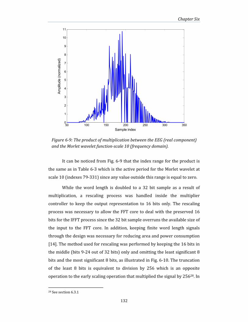
Chapter Six
132
It can be noticed from Fig. 6-9 that the index range for the product is
the same as in Table 6-3 which is the active period for the Morlet wavelet at
scale 10 (indexes 79-331) since any value outside this range is equal to zero.
While the word length is doubled to a 32 bit sample as a result of
multiplication, a rescaling process was handled inside the multiplier
controller to keep the output representation to 16 bits only. The rescaling
process was necessary to allow the FFT core to deal with the preserved 16
bits for the IFFT process since the 32 bit sample overruns the available size of
the input to the FFT core. In addition, keeping finite word length signals
through the design was necessary for reducing area and power consumption
[14]. The method used for rescaling was performed by keeping the 16 bits in
the middle (bits 9-24 out of 32 bits) only and omitting the least significant 8
bits and the most significant 8 bits, as illustrated in Fig. 6-10. The truncation
of the least 8 bits is equivalent to division by 256 which is an opposite
operation to the early scaling operation that multiplied the signal by 25628. In
28 See section 6.3.1
50 100 150 200 250 300 3500
1
2
3
4
5
6
7
8
9
10
11
Sample index
Amplitude (normalized)
Figure 6-9: The product of multiplication between the EEG (real component)
and the Morlet wavelet function-scale 10 (frequency domain).

Chapter Six
133
addition, the 8 least significant bits29 are the least important because they
hold less information and more noise compared with the most significant
bits. The 8 most significant bits are also truncated as long as the product is in
the dynamic range. Therefore, these bits only hold the sign extension and no
useful information exists. The final result was taken to be the 16 bits in the
middle of the multiplication result.
6.3.2.4 Memory Groups
The block RAM provided within the FPGA was used for storing the
data of the EEG signal and the Morlet wavelet, and also for storing the
intermediate data produced whilst processing. The number of memory
blocks (BRAM) needed for the whole design is five (as shown in Fig. 6-6) and
MEM6 is the SRAM ICs (off the FPGA). MEM1 (1K×16 bits) was used to store
the EEG signal and can be addressed by the FFT core. MEM2 (2×1K×16) was
used to store the two components of the EEG in the frequency domain. It was
also addressed by the FFT core. The third block MEM3 (4K×16 bits) contains
the scaled Morlet wavelet in the frequency domain and MEM4 (2×4K×16
bits) contains the product of multiplication between the transformed signals.
29 The truncation of the 8 least bits equates the multiplication by 256 for one of the signals.
As the second signal was also multiplied by 256, this was treated by a division with 256 prior
to displaying the wavelet coefficients.
16 bit signal sample
(frequency domain)
16 bit wavelet sample
(frequency domain)
16 bit x 16 bit
Multiplier
32 bit product
8 LSB (Omitted)
MID 16 bits (result)
8 MSB (Omitted)
Figure 6-10: The multiplication and the truncation procedure

Chapter Six
134
MEM3 and MEM4 are both addressed by the multiplier controller. This is
because the FFT core is idle during multiplications, and a memory larger than
1K cannot be addressed by the FFT core input index of data. MEM5
(2×1K×16 bits) was used as a temporary storage for the wavelet coefficients
in both its real and imaginary components for an individual wavelet scale. It
is addressed by the core at the data unloading stage. Some of these
mentioned memory blocks need to be accessed by more than one side at
different times. For example, the memory that contains the EEG signal in the
frequency domain needs to be accessed by the FFT core through the
unloading process and also accessed later by the multiplier controller to use
the stored data for multiplication. In such a case, multiplexers are used to
switch towards the suitable address source.
For verification and testing purposes, the joint test advisory group
(JTAG) facility of the FPGA was used to access the signals between the
components of the design without resynthesizing and also for checking the
timing schedule and the RAM contents. For example, to test the design with
several EEG epochs, the EEG signal inside the BRAM is changed with the JTAG
facility without the need to resynthesize the design.
Owing to the limited block RAM inside the FPGA (288K×16 bits), the
two SRAM ICs (each 256K×16 bits) on the NanoBoard 3000 are used as a
final storage for the full CWT scalogram (37K×16 bits). The data transfer
controller (Fig. 6-6) was used to transfer a CWT vector from the MEM5 to the
SRAM (MEM6) as long as the vector of these coefficients is available in MEM5.
The transferring details are presented in section 6.5.
6.4 Results
This section presents the numerical results from the CWT system
including synthesis results, timing schedule, and the coefficients of the CWT
presented as scale-based and as a full scalogram. In addition, other design
aspects are also outlined such as the effect of overflow on the outcome etc. In
section 6.5 further optimizations are considered to reduce area and increase
speed.
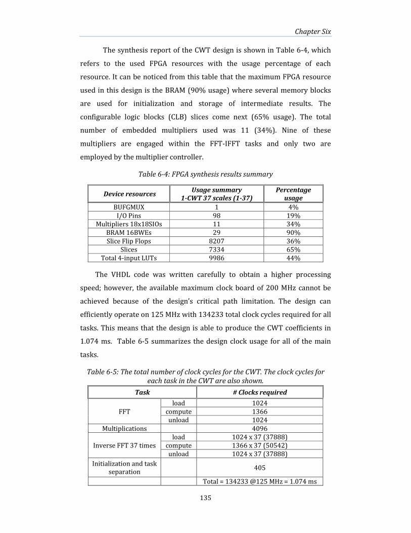
Chapter Six
135
The synthesis report of the CWT design is shown in Table 6-4, which
refers to the used FPGA resources with the usage percentage of each
resource. It can be noticed from this table that the maximum FPGA resource
used in this design is the BRAM (90% usage) where several memory blocks
are used for initialization and storage of intermediate results. The
configurable logic blocks (CLB) slices come next (65% usage). The total
number of embedded multipliers used was 11 (34%). Nine of these
multipliers are engaged within the FFT-IFFT tasks and only two are
employed by the multiplier controller.
Table 6-4: FPGA synthesis results summary
Device resources Usage summary
1-CWT 37 scales (1-37)
Percentage
usage
BUFGMUX 1 4%
I/O Pins 98 19%
Multipliers 18x18SIOs 11 34%
BRAM 16BWEs 29 90%
Slice Flip Flops 8207 36%
Slices 7334 65%
Total 4-input LUTs 9986 44%
The VHDL code was written carefully to obtain a higher processing
speed; however, the available maximum clock board of 200 MHz cannot be
achieved because of the design’s critical path limitation. The design can
efficiently operate on 125 MHz with 134233 total clock cycles required for all
tasks. This means that the design is able to produce the CWT coefficients in
1.074 ms. Table 6-5 summarizes the design clock usage for all of the main
tasks.
Table 6-5: The total number of clock cycles for the CWT. The clock cycles for
each task in the CWT are also shown.
Task # Clocks required
FFT
load 1024
compute 1366
unload 1024
Multiplications 4096
Inverse FFT 37 times
load 1024 x 37 (37888)
compute 1366 x 37 (50542)
unload 1024 x 37 (37888)
Initialization and task
separation 405
Total = 134233 @125 MHz = 1.074 ms

Chapter Six
136
It can be noticed from Table 6-5 that the FFT was performed only once
on the EEG whereas the IFFT was performed 37 times - once per scale. This is
due to the input signal being converted once at the beginning. Some clock
cycles (405 clocks) are also required for initialization and for system tasks
separation as shown in Table 6-5.
A timing simulation test was applied on the design as an operational
verification prior to implementation. To test the correct result from the CWT
calculation, the CWT engine was given the EEG signal in Fig. 6-11 (a). An EEG
of 1024 sample (Fig. 6-11 a) was used to initialize MEM1 in the design (Fig. 6-
6). This signal was produced by recording the Fz brain channel when a
participant was presented with a visual stimulus, and was chosen because it
contains a low frequency component (P300) in addition to the higher
frequencies in the rest of the epoch. The CWT engine analyses this signal
using the Morlet wavelet and produces the CWT coefficients at different
scales. The CWT coefficients at scales 13-37 contain the EEG frequencies 2-
120 Hz. Typical EEG frequencies of less than 50 Hz are within the range 19-
37 of the scales. Fig 6-11 (b) shows the real and imaginary components of
these coefficients at scale 31 (corresponds to 5.52 Hz) after the CWT was
applied. The magnitude at the same scale is shown in Fig. 6-11 (c). It can be
noticed from Fig. 6-11 (c) that the representation of the wavelet magnitude
reflects the amplitude of the original EEG (Fig. 6-11 a). The generation of the
CWT coefficients in Fig. 6-11 (c) is repeated for all the engaged scales to give
the full CWT scalogram.
The obtained CWT coefficients at each scale are matched to the
theoretical values computed by Matlab software. Owing to the quantization
error produced through the FFT core and the rescaling process after
multiplication, the hardware results have a slight difference compared to the
software result. For example, Fig. 6-12 shows the CWT coefficients produced
by both the FPGA and Matlab at scale 20 for the same EEG in Fig. 6-11 (a).
This figure clearly shows the accuracy of the wavelet coefficients based on
hardware implementation. All the hardware based wavelet coefficients at the
37 scales were verified with their software counterparts as explained in the
next paragraph.

Chapter Six
137
Figure 6-11: (a) an EEG signal showing an ERP from the visual stimulus
test. (b) The real and imaginary CWT components of the EEG at scale 31.
(c) The CWT magnitude-scale 31 (one scale band).
0 100 200 300 400 500 600 700 800 900 1000-20
0
20
40
60
(a)
Amplitude [uV]
0 100 200 300 400 500 600 700 800 900 1000-100
-50
0
50
100
(b)
Amplitude
0 100 200 300 400 500 600 700 800 900 100020
40
60
80
Time [ms](c)
Amplitude
Real CWT
Imag. CWT
EEG signal
CWT magnitude, scale 31
0 100 200 300 400 500 600 700 800 900 10000
2
4
6
8
10
12
Time [ms]
Magnitude
FPGA
Matlab
Figure 6-12: The CWT coefficients (magnitude) at scale 20 produced by
both Matlab software and FPGA.

Chapter Six
138
Matlab was used to generate the CWT for the same input signal which was
used as the reference. The hardware CWT run and the results between
hardware and software were compared. To verify the results of the CWT, the
correlation coefficient was calculated on the CWT module at each scale
between the methods of hardware and software implementation. Table 6-6
lists these correlations at these scales (scales 5 and 10 were listed as low
scales and the rest of the scales 17-37 were listed corresponding to the EEG
frequencies 1.9-62.5 Hz). At low scales such as 5, no frequency components
of the EEG exist, therefore the correlation coefficient is low due to the
presenting noise instead. In the typical EEG frequency band range (1.9-62.5
Hz), the correlation coefficient obtained in Table 6-6 shows the closeness
between the FPGA output and Matlab output. The high correlation between
hardware and software results in the “correlation coefficients” column is an
objective measure on the accuracy of the implemented hardware.
Table 6-6: The correlation coefficients between software and hardware CWT at
scales 5, 10, 15 and 17-37
Wavelet scale
number
Corresponding
frequency [Hz]
EEG
band
Correlation coefficients of
CWT between hardware and
software (0-1)
5 500 γ 0.7532
10 208.33 γ 0.9199
15 88.49 γ 0.9821
17 62.5 γ 0.9980
18 52.63 γ 0.9996
19 44.24 γ 0.9997
20 37.17 γ 0.9995
21 31.25 γ 0.9993
22 26.24 β 0.9989
23 22.07 β 0.9992
24 18.58 β 0.9997
25 15.62 β 0.9998
26 13.14 β 0.9999
27 11.05 α 1
28 9.29 α 0.9999
29 7.81 θ 0.9989
30 6.57 θ 0.9802
31 5.52 θ 1
32 4.64 θ 1
33 3.9 δ 1
34 3.28 δ 1
35 2.76 δ 1
36 2.32 δ 1
37 1.95 δ 1

Chapter Six
139
The difference between the hardware CWT compared to the
theoretical Matlab values is that the hardware has a higher quantization
error due to the larger approximation in representing samples occurring by
fraction removal. In addition, the multiplier truncation and the rescaling
process by the FFT core (see Fig. 4-17) add further quantization errors. The
higher correlation values (> 0.98 at scales 15-37) were specifically obtained
at high scales (low frequencies) in which most frequencies of the ERP signal
were concentrated. This is because the ERP component in Fig. 6-11 (a) has a
higher amplitude than the rest of the EEG so it’s less affected by the
quantization errors and hardware rescaling processes. The reduction in these
errors increases the shape similarity of the hardware wavelet coefficients, i.e.
less noise, with that produced by software (Matlab). At low scales, lower
correlations were obtained (< 0.98) (see Table 6-6, column 4, scales 5 and
10) where the ERP component does not exist at the corresponding
frequencies to these scales. The accuracy of the full CWT scalogram was also
measured using image quality methods discussed later in this chapter.
Regarding the probability of overflow occurrence, it is worthwhile to
mention that this matter is subject to the values chosen to bias the EEG and
the Morlet wavelet as a requirement of hardware representation. When both
functions are multiplied by 28 (256), an overflow appears at the higher scales
where the amplitude of both the EEG and the Morlet counterpart is maximum
(see Fig. 4-16 and Fig. 6-5). As a result, some of the hardware CWT
coefficients are incorrectly computed over six of these scales (out of 37).
Thus, an adjustment was made to reduce the biasing of the Morlet to avoid
the appearance of overflow or underflow in the CWT coefficients. The chosen
value of 256 was reduced as a final maximum biasing value to 194 whereas
the EEG stayed in the biasing of 256. Fig. 6-13 shows an overflow case in the
wavelet coefficients at scale 31 where a distortion appeared in these
coefficients around the period 600-800 ms in the form of a zigzag trend. This
is successfully treated with the new proposed biasing shown in Fig. 6-11 (c)
where the correct computation of the CWT at this scale is shown. The y-axis
difference between Fig. 6-11 (c) and Fig. 6-13 is due to showing Fig. 6-13
prior to re-biasing (re-scaling).

Chapter Six
140
6.5 Design Modification and Improvement
This section presents further improvements to the CWT engine to
improve performance speed while reducing design complexity and resource
requirements. The improvement is performed by using the SRAM ICs and
also specifies the design to analyse signals in the EEG typical frequencies.
6.5.1 Static RAM Controller
The SRAM on the Altium NanoBoard [15] outside the FPGA are used
because the rest of the available BRAM is not enough to store the CWT
coefficients on the size of two 375�@a� × 1024¦b67� × 16B6� (2 × 37K
points). For that, two BRAMs (each 1½ × 16 bits) are used to temporarily
store the wavelet coefficients at individual scales after the completion of
every inverse FFT process, one of them for the real CWT component and the
other for the imaginary component. While the FFT core loads new data and
computes the inverse FFT of that data for the next scale, the CWT coefficients
inside the BRAM are transferred into the SRAM. Before unloading a new scale
of wavelet coefficients, the FFT core requires 1024 clock cycles for loading +
1366 clock cycles for computation = 2390 clock cycles. The real and
imaginary CWT coefficients are transferred from the BRAM into the SRAM in
Figure 6-13: The effect of overflow on the CWT coefficients-scale 31-
based on FPGA.
0 100 200 300 400 500 600 700 800 900 10001
1.5
2
2.5
3
3.5
4x 10
4
Time [ms]
Amplitude
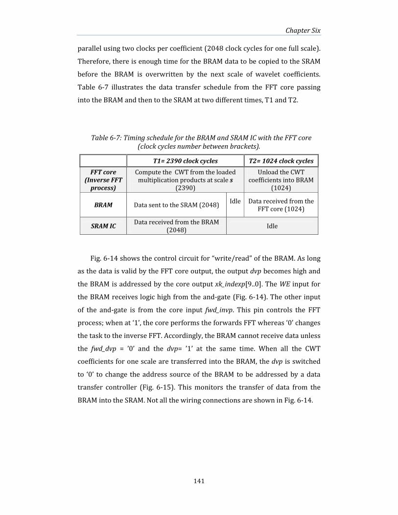
Chapter Six
141
parallel using two clocks per coefficient (2048 clock cycles for one full scale).
Therefore, there is enough time for the BRAM data to be copied to the SRAM
before the BRAM is overwritten by the next scale of wavelet coefficients.
Table 6-7 illustrates the data transfer schedule from the FFT core passing
into the BRAM and then to the SRAM at two different times, T1 and T2.
Table 6-7: Timing schedule for the BRAM and SRAM IC with the FFT core
(clock cycles number between brackets).
Fig. 6-14 shows the control circuit for “write/read” of the BRAM. As long
as the data is valid by the FFT core output, the output dvp becomes high and
the BRAM is addressed by the core output xk_indexp[9..0]. The WE input for
the BRAM receives logic high from the and-gate (Fig. 6-14). The other input
of the and-gate is from the core input fwd_invp. This pin controls the FFT
process; when at ‘1’, the core performs the forwards FFT whereas ‘0’ changes
the task to the inverse FFT. Accordingly, the BRAM cannot receive data unless
the fwd_dvp = ’0’ and the dvp= ’1’ at the same time. When all the CWT
coefficients for one scale are transferred into the BRAM, the dvp is switched
to ‘0’ to change the address source of the BRAM to be addressed by a data
transfer controller (Fig. 6-15). This monitors the transfer of data from the
BRAM into the SRAM. Not all the wiring connections are shown in Fig. 6-14.
T1= 2390 clock cycles T2= 1024 clock cycles
FFT core
(Inverse FFT
process)
Compute the CWT from the loaded
multiplication products at scale s
(2390)
Unload the CWT
coefficients into BRAM
(1024)
BRAM Data sent to the SRAM (2048) Idle
Data received from the
FFT core (1024)
SRAM IC Data received from the BRAM
(2048) Idle
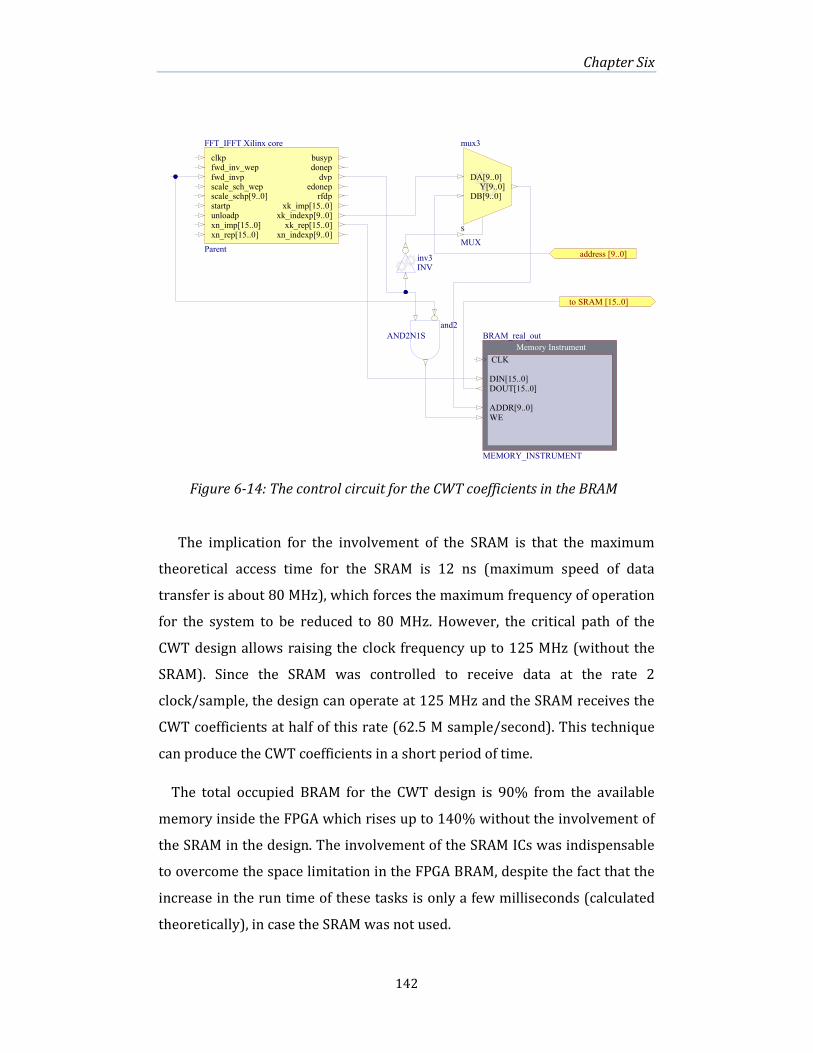
Chapter Six
142
The implication for the involvement of the SRAM is that the maximum
theoretical access time for the SRAM is 12 ns (maximum speed of data
transfer is about 80 MHz), which forces the maximum frequency of operation
for the system to be reduced to 80 MHz. However, the critical path of the
CWT design allows raising the clock frequency up to 125 MHz (without the
SRAM). Since the SRAM was controlled to receive data at the rate 2
clock/sample, the design can operate at 125 MHz and the SRAM receives the
CWT coefficients at half of this rate (62.5 M sample/second). This technique
can produce the CWT coefficients in a short period of time.
The total occupied BRAM for the CWT design is 90% from the available
memory inside the FPGA which rises up to 140% without the involvement of
the SRAM in the design. The involvement of the SRAM ICs was indispensable
to overcome the space limitation in the FPGA BRAM, despite the fact that the
increase in the run time of these tasks is only a few milliseconds (calculated
theoretically), in case the SRAM was not used.
clkpfwd_inv_wepfwd_invpscale_sch_wepscale_schp[9..0]startpunloadpxn_imp[15..0]xn_rep[15..0]
busypdonepdvp
edoneprfdp
xk_imp[15..0]xk_indexp[9..0]xk_rep[15..0]
xn_indexp[9..0]
FFT_IFFT Xilinx core
Parent
DA[9..0]
DB[9..0]Y[9..0]
S
mux3
MUX
inv3INV
and2
AND2N1S
Memory Instrument
CLK
DIN[15..0]DOUT[15..0]
ADDR[9..0]WE
BRAM_real_out
MEMORY_INSTRUMENT
address [9..0]
to SRAM [15..0]
Figure 6-14: The control circuit for the CWT coefficients in the BRAM

Chapter Six
143
A
The schematic that includes the data transfer controller (block B) and the
SRAM ICs is shown in Fig. 6-15. Block B reads the CWT coefficients from the
BRAM (inside the red circle in block A) and sends it to block C (SRAM ICs).
The figure shows the connection of block B and C with the CWT engine (block
A).
B
CLK_BRD
SW_USER0
UI
INV
UA
AND2S
inv2
INV
SW_USER1
SW[7..0]
ON
12
34
56
78
I[7..0]O0
O1O2O3
O4O5
O6O7 Ud
J8B_8S
SRAM0_ESRAM0_A[17..0]
SRAM0_WSRAM0_OESRAM0_UB
SRAM0_D[15..0]
SRAM0_LB
ISSI
IS61LV25616AL-10TL
SRAM1_E
SRAM1_A[17..0]
SRAM1_W
SRAM1_OESRAM1_UB
SRAM1_D[15..0]
SRAM1_LB
ISSI
IS61LV25616AL-10TL
GND
[15..0]
[15..0]
buff2
IOBUF16B
[15..0]
[15..0]
buff3
IOBUF16B
Configurable Digital IO
scale_No[5..0]
Real_data[15..0]bram_address[9..0]sram_address[17..0]
trig_sel
ioSram
DIGITAL_IO
DA[17..0]
DB[17..0]Y[17..0]
S
mux5
MUX
DA
DBY
S
mux6
MUX
cntrl
real_data[15..0]
address[9..0]
imag_data[15..0]clkrststart_cwt_cntrlr
U_Wcoherence
Wcoherence.SchDoc
address_bram[9..0]
address_sram[17..0]
clk
cntrlrd_sramrst
scale[5..0]
trig_slr
vreal_data_bram[15..0]
vreal_data_sram[15..0]wr_sram
ximag_data_bram[15..0]
ximag_data_sram[15..0]
VHDLENTITY: bram_sram
U_bram_sram
SLR_CWT_16_March_2012.vhd
/ 2
cd1CDIV2DC50
DA[15..0]
DB[15..0]
Y[15..0]
S
mux7MUX
DA[15..0]
DB[15..0]
Y[15..0]
S
mux8MUXGND
selsram_din[15..0]
sram_dout1[15..0]sram_dout2[15..0]
VHDLENTITY: muxU_mux
mux_cct.vhd
selsram_din[15..0]
sram_dout1[15..0]sram_dout2[15..0]
VHDLENTITY: mux
U_mux2mux_cct.vhd
clkpfwd_inv_wep
fwd_invpscale_sch_wep
scale_schp[ 9..0]st ar tpunloadp
xn_imp[ 15..0]xn_rep[15.. 0]
busypdonep
dvpedonep
r fdpxk_imp[ 15..0]
xk_in dexp[ 9..0]
xk_r ep[ 15..0]xn_in dexp[ 9..0]
FFT_IFF T
Parent
Conf igurable Digital IO
busydone
dvedone
r fdxk_im [15..0]xk_in dex[ 9..0]
xk_r e[15..0]xn_in dex[ 9..0]
core_monit oring
DIGI TAL_IO
Memory Ins trum ent
CLK
DIN[7..0]DOUT[7..0]
ADDR[9..0]
WE
LSB2
MEMORY_INSTRUMENT
GND
Memory Ins trum ent
CLK
DIN[7..0]
DOUT[7..0]
ADDR[9..0]WE
MSB2
MEMORY_INSTRUMENT
GND
O[15..0] I A[7..0]
I B[ 7..0]sp_input2
J8B2_16B
I0I1
I2
O[2. .0]
join
J3S_3B
Configur able Di gital IO
IM_to_core[15..0]
Re_t o_cor e[ 15..0]scl_No[ 4..0]
monitor 2
DIGITAL_IO
Memory Ins trum ent
CLK
DIN[7..0]DOUT[7..0]
ADDR[9..0]
WE
IM_LSB_ff t
MEMORY_INSTRUMENT
Memor y Ins trument
CLK
DIN[7..0]DOUT[7..0]
ADDR[9..0]
WE
RE_LSB_ff t
MEMORY_INSTRUMENT
Memor y Ins trument
CLK
DIN[7..0]DOUT[7..0]
ADDR[9..0]
WE
RE_MSB_ff t
MEMORY_INSTRUMENT
Memory Ins trum ent
CLK
DIN[7..0]DOUT[7..0]
ADDR[9..0]
WE
IM_MSB_ff t
MEMORY_INSTRUMENT
I[15..0] OA[7..0]
OB[ 7..0]
sp1
J16B_8B2
I [15..0] OA[ 7..0]
OB[7. .0]
sp2
J16B_8B2
O[15..0] IA[7..0]
IB[7..0]sp3
J8B2_16B
O[15..0] IA[7..0]
IB[7..0]sp4
J8B2_16B
A[15 ..0 ]
B[15..0 ]
Y[15..0 ]
S0
mux1
M16_B2B1
Memory I nstr ument
CLK
DIN[7. .0]
DOUT[7 ..0]
ADDR[ 8..0]WE
wav_scl10_LSB
MEMORY_INS TRUMENT
Memory I nstr ument
CLK
DIN[7. .0]DOUT[7 ..0]
ADDR[ 8..0]
WE
wav_scl10_msb
MEMORY_INS TRUMENT
O[15.. 0] IA[7 ..0]
IB[7..0]wav
J8B2_16B
GND
GND
Memor y Ins trument
CLK
DIN[ 7..0]
DOUT[ 7..0]
ADDR[8..0]WE
real_result_LSB
MEMORY_INS TRUMENT
Memor y Ins trument
CLK
DIN[ 7..0]DOUT[ 7..0]
ADDR[8..0]WE
real_result_MSB
MEMORY_INS TRUMENT
Memory I nst rument
CLK
DIN[ 7..0]
DOUT[ 7..0]
ADDR[ 8..0]WE
Imag_r esult_LSB
MEMORY_INS TRUMENT
Memory I nst rument
CLK
DIN[ 7..0]DOUT[ 7..0]
ADDR[ 8..0]WE
Imad_r esult_MSB
MEMORY_INS TRUMENT
I [15..0] OA[ 7..0]
OB[7..0]
sp5
J16B_8B2
I[15..0] OA[7..0]
OB[ 7..0]
sp6
J16B_8B2
O[15..0] IA[7..0]
IB[7..0]sp7
J8B2_16B
O[15..0] I A[7..0]
I B[ 7..0]sp8
J8B2_16B
address_ff t_si g[9..0]
address_mor let [8..0]address_mu l_result [8..0]
clk
fr om_cwt_ hsim_inp[ 15..0]
im_out [15..0]morlet[ 15..0]
re_inp[15. .0] r e_out [15..0]rs t to_cwt_hs
wr ite_enable
VHDLENTITY: mult_coherence
U_mult_coherencemul_wcoherence.vhd
A [9..0]
B[9 ..0]
Y [9..0 ]
S0
mux2
M10 _B2B1
A [8..0 ]
B [8..0]
Y[8 ..0 ]
S0
mux3
M9_B2B1
Configurable Digital I O
hs1
hs2addr ess_fft_m em [9..0]
addr ess_Mor let[8..0]addr ess_af ter_mul[ 8..0]
m onitor3
DIGITAL_IO
address_aft er _mul[8..0]
address_f ft_mem[9..0]
clk
eeg_self ft_cntr l_signals [2..0]
ff t_st ar t
f rom_mul _hs
fwd_inv
fwd_inv_we
i m_core_dat a[ 15..0]
im_f ft[15..0]
im_out[15..0]
i mag_mult_result[15..0]
mul_r eset
r e_cor e_data[ 15..0]
re_f ft[15. .0]
r e_inp[15..0]
re_out[15.. 0]
r eal _mult_result[15..0]r st
scale_no[4..0]
scl_sch_core[9..0]scl_sch_we
start_cwt_cntrl r
to_m ul_handshakewe_ff t_mem
xk_ addr ess[9..0]xn_ addr ess[9..0]
VHDLENTITY: contr _sr am
U_contr _sr am
wcoherence2.vhd
Memory I nst rument
CLK
DIN[ 7..0]DOUT[ 7..0]
ADDR[ 9..0]
WE
LSB
MEMORY_INS TRUMENT
GND
Memory I nst rument
CLK
DIN[ 7..0]
DOUT[ 7..0]
ADDR[ 9..0]WE
MSB
MEMORY_INS TRUMENT
GND
O[15..0] IA[7..0]
IB[7..0]sp_input
J8B2_16B
Memor y Ins trument
CLK
DIN[7..0]DOUT[7..0]
ADDR[9..0]
WE
r eal_out put_LSB
MEMORY_INSTRUMENT
Memor y Ins trument
CLK
DIN[7..0]DOUT[7..0]
ADDR[9..0]
WE
r eal_out put_MSB
MEMORY_INSTRUMENT
and2AND2N1S
DA[9..0]
DB[9..0]
Y[ 9..0]
S
mux4
MUX
i nv3
INV
I [15..0] OA[7 ..0]
OB[7..0]
j1
J16B_8B2
O[ 15..0]I A[7..0]
IB[7..0]
j3
J8B2_16B
cnt rl
real_data[ 15..0]
address[9..0]
Mem ory Ins trument
CLK
DIN[7..0]DOUT[7..0]
ADDR[9..0]
WE
i mag_out put_LSB
MEMORY_INSTRUMENT
Mem ory Ins trument
CLK
DIN[7..0]
DOUT[7..0]
ADDR[9..0]WE
i mag_out put_MSB
MEMORY_INSTRUMENT
I [15..0] OA[ 7..0]
OB[7..0]
j1_img
J16B_8B2
O[15..0]IA[7..0]
IB[7..0]
j3_img
J8B2_16B
imag_data[ 15..0]
clk
rs t
s tart_cwt_cntrlr
address_bram[9..0]address_sram[17..0]
clkcntrl
rd_sramrstscale[5..0]
trig_slrvreal_data_bram[15..0]
vreal_data_sram[15..0]wr_sram
ximag_data_bram[15..0]
ximag_data_sram[15..0]
VHDLENTITY: bram_sram
SLR_CWT_16_March_2012.vhd
SRAM0_ESRAM0_A[17..0]
SRAM0_WSRAM0_OESRAM0_UB
SRAM0_D[15..0]
SRAM0_LB
ISSI
IS61LV25616AL-10TL
SRAM1_ESRAM1_A[17..0]
SRAM1_WSRAM1_OESRAM1_UB
SRAM1_D[15..0]
SRAM1_LB
ISSI
IS61LV25616AL-10TL
C: The SRAM ICs
B: Data transfer Controller
Figure 6-15: A design schematic sheet contains the CWT engine, data transfer
controller & the SRAM ICs with the circle areas magnified to show these
components.
C
A: The CWT Engine (see Fig. 6-7)
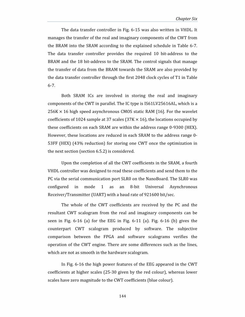
Chapter Six
144
The data transfer controller in Fig. 6-15 was also written in VHDL. It
manages the transfer of the real and imaginary components of the CWT from
the BRAM into the SRAM according to the explained schedule in Table 6-7.
The data transfer controller provides the required 10 bit-address to the
BRAM and the 18 bit-address to the SRAM. The control signals that manage
the transfer of data from the BRAM towards the SRAM are also provided by
the data transfer controller through the first 2048 clock cycles of T1 in Table
6-7.
Both SRAM ICs are involved in storing the real and imaginary
components of the CWT in parallel. The IC type is IS61LV25616AL, which is a
256K×16 high speed asynchronous CMOS static RAM [16]. For the wavelet
coefficients of 1024 sample at 37 scales (37K× 16), the locations occupied by
these coefficients on each SRAM are within the address range 0-9300 (HEX).
However, these locations are reduced in each SRAM to the address range 0-
53FF (HEX) (43% reduction) for storing one CWT once the optimization in
the next section (section 6.5.2) is considered.
Upon the completion of all the CWT coefficients in the SRAM, a fourth
VHDL controller was designed to read these coefficients and send them to the
PC via the serial communication port SLR0 on the NanoBoard. The SLR0 was
configured in mode 1 as an 8-bit Universal Asynchronous
Receiver/Transmitter (UART) with a baud rate of 921600 bit/sec.
The whole of the CWT coefficients are received by the PC and the
resultant CWT scalogram from the real and imaginary components can be
seen in Fig. 6-16 (a) for the EEG in Fig. 6-11 (a). Fig. 6-16 (b) gives the
counterpart CWT scalogram produced by software. The subjective
comparison between the FPGA and software scalograms verifies the
operation of the CWT engine. There are some differences such as the lines,
which are not as smooth in the hardware scalogram.
In Fig. 6-16 the high power features of the EEG appeared in the CWT
coefficients at higher scales (25-30 given by the red colour), whereas lower
scales have zero magnitude to the CWT coefficients (blue colour).
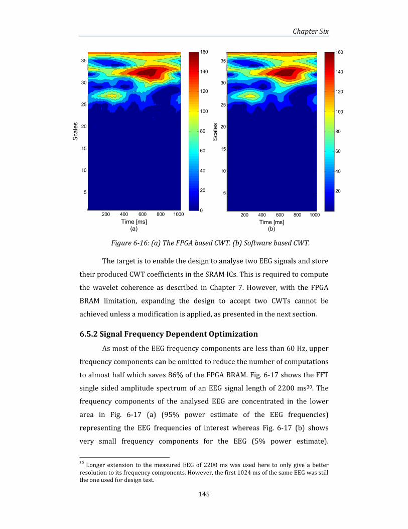
Chapter Six
145
The target is to enable the design to analyse two EEG signals and store
their produced CWT coefficients in the SRAM ICs. This is required to compute
the wavelet coherence as described in Chapter 7. However, with the FPGA
BRAM limitation, expanding the design to accept two CWTs cannot be
achieved unless a modification is applied, as presented in the next section.
6.5.2 Signal Frequency Dependent Optimization
As most of the EEG frequency components are less than 60 Hz, upper
frequency components can be omitted to reduce the number of computations
to almost half which saves 86% of the FPGA BRAM. Fig. 6-17 shows the FFT
single sided amplitude spectrum of an EEG signal length of 2200 ms30. The
frequency components of the analysed EEG are concentrated in the lower
area in Fig. 6-17 (a) (95% power estimate of the EEG frequencies)
representing the EEG frequencies of interest whereas Fig. 6-17 (b) shows
very small frequency components for the EEG (5% power estimate).
30
Longer extension to the measured EEG of 2200 ms was used here to only give a better
resolution to its frequency components. However, the first 1024 ms of the same EEG was still
the one used for design test.
Time [ms](a)
Scales
200 400 600 800 1000
5
10
15
20
25
30
35
0
20
40
60
80
100
120
140
160
Time [ms](b)
Scales
200 400 600 800 1000
5
10
15
20
25
30
35
20
40
60
80
100
120
140
160
Figure 6-16: (a) The FPGA based CWT. (b) Software based CWT.
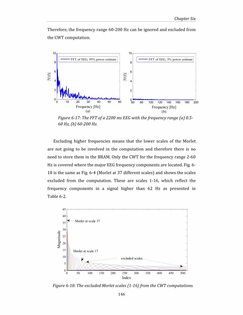
Chapter Six
146
Therefore, the frequency range 60-200 Hz can be ignored and excluded from
the CWT computation.
Excluding higher frequencies means that the lower scales of the Morlet
are not going to be involved in the computation and therefore there is no
need to store them in the BRAM. Only the CWT for the frequency range 2-60
Hz is covered where the major EEG frequency components are located. Fig. 6-
18 is the same as Fig. 6-4 (Morlet at 37 different scales) and shows the scales
excluded from the computation. These are scales 1-16, which reflect the
frequency components in a signal higher than 62 Hz as presented in
Table 6-2.
0 10 20 30 40 50 600
2
4
6
8
10
Frequency [Hz](a)
|Y(f)|
60 80 100 120 140 160 180 2000
2
4
6
8
10
Frequency [Hz](b)
|Y(f)|
FFT of EEG, 95% power estimate FFT of EEG, 5% power estimate
Figure 6-17: The FFT of a 2200 ms EEG with the frequency range (a) 0.5-
60 Hz, (b) 60-200 Hz.
0 50 100 150 200 250 300 350 400 450 5000
5
10
15
20
25
30
35
40
45
Index
Magnitude
Morlet at scale 17
Morlet at scale 37
excluded scales
Figure 6-18: The excluded Morlet scales (1-16) from the CWT computations.
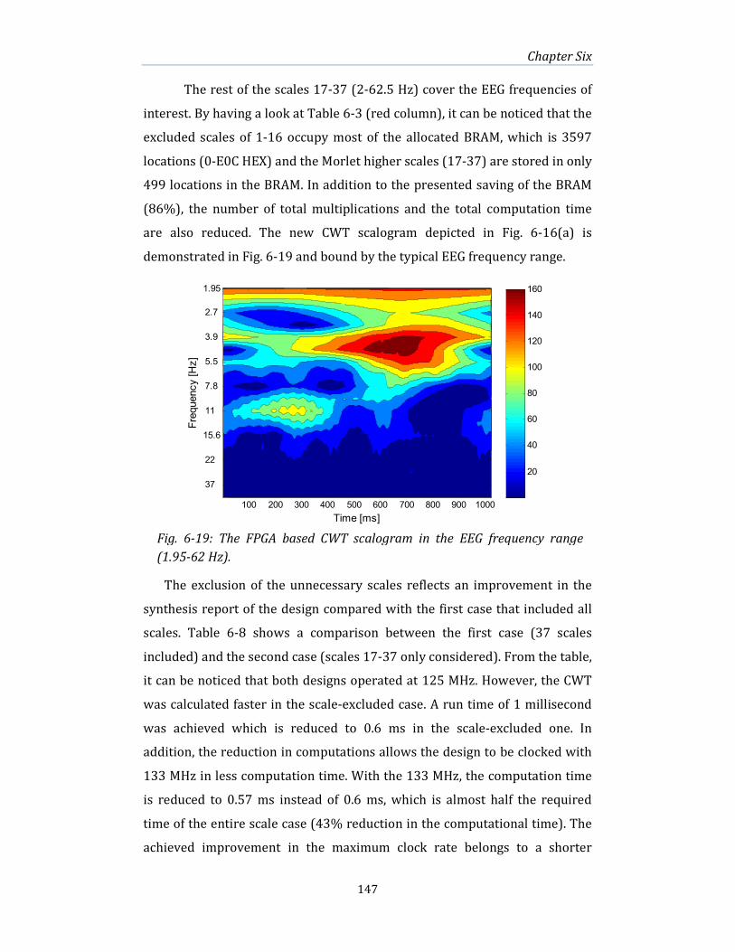
Chapter Six
147
The rest of the scales 17-37 (2-62.5 Hz) cover the EEG frequencies of
interest. By having a look at Table 6-3 (red column), it can be noticed that the
excluded scales of 1-16 occupy most of the allocated BRAM, which is 3597
locations (0-E0C HEX) and the Morlet higher scales (17-37) are stored in only
499 locations in the BRAM. In addition to the presented saving of the BRAM
(86%), the number of total multiplications and the total computation time
are also reduced. The new CWT scalogram depicted in Fig. 6-16(a) is
demonstrated in Fig. 6-19 and bound by the typical EEG frequency range.
The exclusion of the unnecessary scales reflects an improvement in the
synthesis report of the design compared with the first case that included all
scales. Table 6-8 shows a comparison between the first case (37 scales
included) and the second case (scales 17-37 only considered). From the table,
it can be noticed that both designs operated at 125 MHz. However, the CWT
was calculated faster in the scale-excluded case. A run time of 1 millisecond
was achieved which is reduced to 0.6 ms in the scale-excluded one. In
addition, the reduction in computations allows the design to be clocked with
133 MHz in less computation time. With the 133 MHz, the computation time
is reduced to 0.57 ms instead of 0.6 ms, which is almost half the required
time of the entire scale case (43% reduction in the computational time). The
achieved improvement in the maximum clock rate belongs to a shorter
Time [ms]
Frequency [Hz]
100 200 300 400 500 600 700 800 900 1000
37
22
15.6
11
7.8
5.5
3.9
2.7
1.95
20
40
60
80
100
120
140
160
Fig. 6-19: The FPGA based CWT scalogram in the EEG frequency range
(1.95-62 Hz).
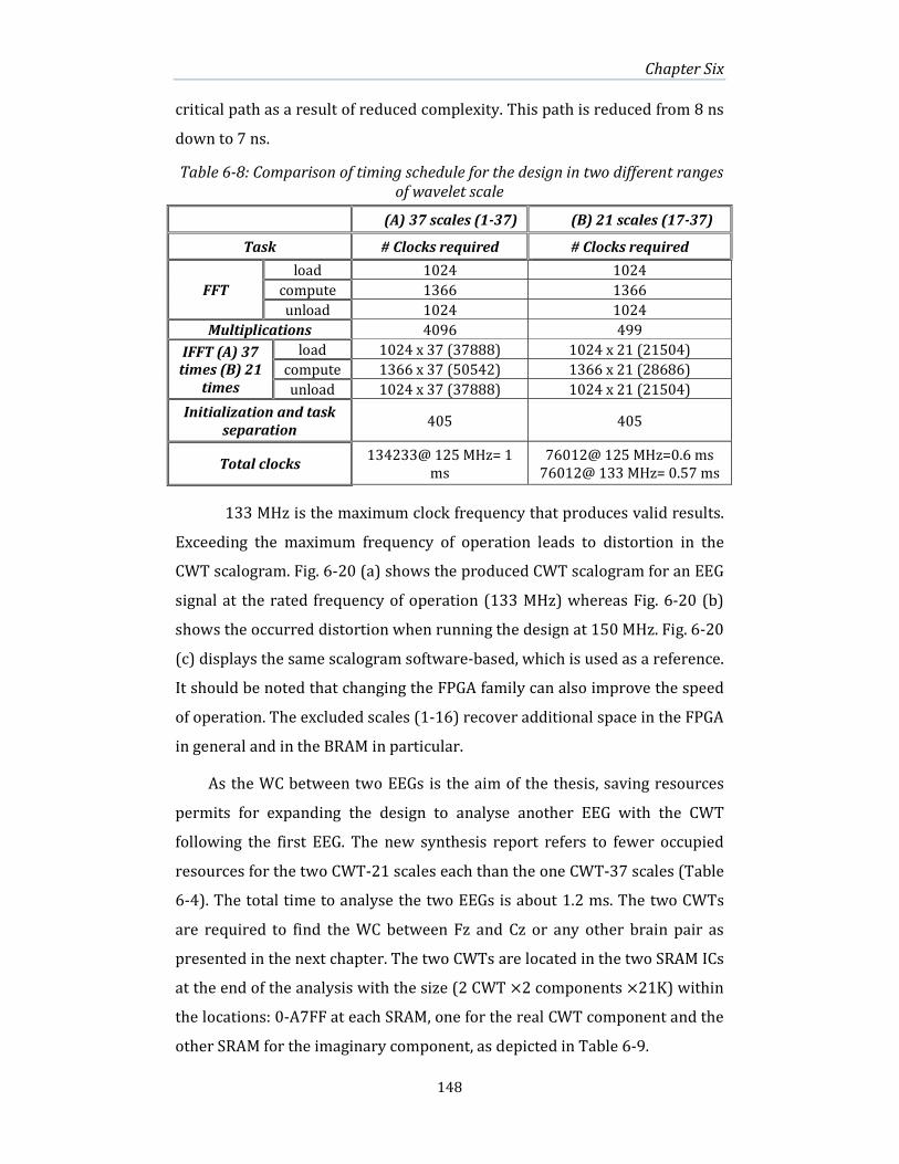
Chapter Six
148
critical path as a result of reduced complexity. This path is reduced from 8 ns
down to 7 ns.
Table 6-8: Comparison of timing schedule for the design in two different ranges
of wavelet scale
133 MHz is the maximum clock frequency that produces valid results.
Exceeding the maximum frequency of operation leads to distortion in the
CWT scalogram. Fig. 6-20 (a) shows the produced CWT scalogram for an EEG
signal at the rated frequency of operation (133 MHz) whereas Fig. 6-20 (b)
shows the occurred distortion when running the design at 150 MHz. Fig. 6-20
(c) displays the same scalogram software-based, which is used as a reference.
It should be noted that changing the FPGA family can also improve the speed
of operation. The excluded scales (1-16) recover additional space in the FPGA
in general and in the BRAM in particular.
As the WC between two EEGs is the aim of the thesis, saving resources
permits for expanding the design to analyse another EEG with the CWT
following the first EEG. The new synthesis report refers to fewer occupied
resources for the two CWT-21 scales each than the one CWT-37 scales (Table
6-4). The total time to analyse the two EEGs is about 1.2 ms. The two CWTs
are required to find the WC between Fz and Cz or any other brain pair as
presented in the next chapter. The two CWTs are located in the two SRAM ICs
at the end of the analysis with the size (2 CWT ×2 components ×21K) within
the locations: 0-A7FF at each SRAM, one for the real CWT component and the
other SRAM for the imaginary component, as depicted in Table 6-9.
(A) 37 scales (1-37) (B) 21 scales (17-37)
Task # Clocks required # Clocks required
FFT
load 1024 1024
compute 1366 1366
unload 1024 1024
Multiplications 4096 499
IFFT (A) 37
times (B) 21
times
load 1024 x 37 (37888) 1024 x 21 (21504)
compute 1366 x 37 (50542) 1366 x 21 (28686)
unload 1024 x 37 (37888) 1024 x 21 (21504)
Initialization and task
separation 405 405
Total clocks 134233@ 125 MHz= 1
ms
76012@ 125 MHz=0.6 ms
76012@ 133 MHz= 0.57 ms

Chapter Six
149
Figure 6-20: The CWT scalogram for an EEG signal (a)31 FPGA based @133
MHz. (b) FPGA based @ 150 MHz-distortion takes place. (c) Software based.
31 Some distortion appears at the top of this figure due to an overflow occurrence.
Time [ms](b)
Frequency [Hz]
100 200 300 400 500 600 700 800 900 1000
52.6
37.17
26.24
18.58
13.14
9.29
6.57
4.64
3.28
2.32
20
40
60
80
100
120
140
160
180
200
Time [ms](c)
Frequency [Hz]
100 200 300 400 500 600 700 800 900 1000
52.6
37.17
26.24
18.58
13.14
9.29
6.57
4.64
3.28
2.32
20
40
60
80
100
120
140
160
180
200
Time [ms](a)
Frequency [Hz]
100 200 300 400 500 600 700 800 900 1000
52.6
37.17
26.24
18.58
13.14
9.29
6.57
4.64
3.28
2.32
20
40
60
80
100
120
140
160
180
200

Chapter Six
150
Table 6-9: The locations of the CWT coefficients in SRAM0 & SRAM1 ICs
SRAM0 Addresses (HEX) Stored data
0-53FF CWT1-real component
5400-A7FF CWT2-real component
SRAM1 Addresses (HEX) Stored data
0-53FF CWT1- imaginary component
5400-A7FF CWT2-imaginary component
Table 6-10 shows that the scale-excluded case for two CWT-21 scale
designs required fewer FPGA resources compared to one CWT-37 scale
design (Table 6-4). The I/O pins and the multipliers used are still the same in
both cases; however, the BRAM, the slices and the total LUTs have reduced
percentages of usage in the scale-excluded two CWT designs. This is ascribed
to the reduced amount of computations on the input signal leading to less
memory usage and a smaller number of LUTs needed. Without the exclusion
of scales 1-16, expanding the design to analyse two EEGs was restricted by
the available FPGA resources. The ignored scales have no serious effect on
the useful data or the accuracy of the CWT scalogram as can be seen from Fig.
6-19 where the typical EEG frequency range is included.
Table 6-10: The FPGA synthesis report of the design in two EEG signals to be
analysed with the included Morlet wavelet scales.
6.6 Scalogram Quality Measures
The subjective comparison between hardware and software
scalogram plots in Fig. 6-16 shows some differences in the smoothness of the
lines between colours and the ripples around the existent islands in the plot.
2 CWT- 21 scales (17-37)
Device resources Usage summary % usage
I/O pins 98 19%
Multipliers 18x18 11 34%
RamB16BWEs 25 78%
Slices 6964 61%
Total 4-input LUTs 9180 40%
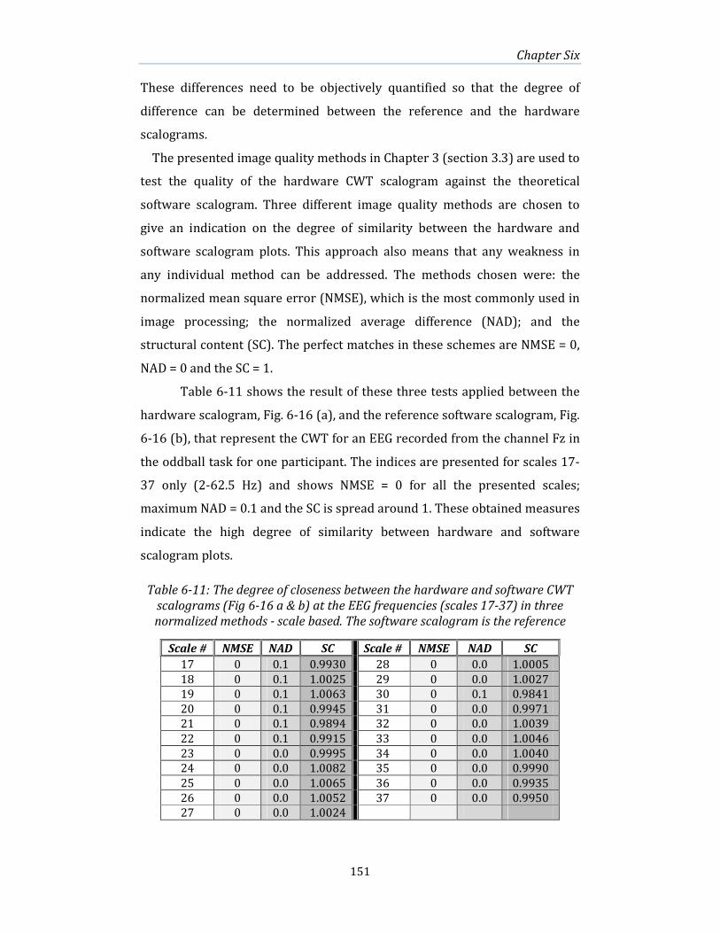
Chapter Six
151
These differences need to be objectively quantified so that the degree of
difference can be determined between the reference and the hardware
scalograms.
The presented image quality methods in Chapter 3 (section 3.3) are used to
test the quality of the hardware CWT scalogram against the theoretical
software scalogram. Three different image quality methods are chosen to
give an indication on the degree of similarity between the hardware and
software scalogram plots. This approach also means that any weakness in
any individual method can be addressed. The methods chosen were: the
normalized mean square error (NMSE), which is the most commonly used in
image processing; the normalized average difference (NAD); and the
structural content (SC). The perfect matches in these schemes are NMSE = 0,
NAD = 0 and the SC = 1.
Table 6-11 shows the result of these three tests applied between the
hardware scalogram, Fig. 6-16 (a), and the reference software scalogram, Fig.
6-16 (b), that represent the CWT for an EEG recorded from the channel Fz in
the oddball task for one participant. The indices are presented for scales 17-
37 only (2-62.5 Hz) and shows NMSE = 0 for all the presented scales;
maximum NAD = 0.1 and the SC is spread around 1. These obtained measures
indicate the high degree of similarity between hardware and software
scalogram plots.
Table 6-11: The degree of closeness between the hardware and software CWT
scalograms (Fig 6-16 a & b) at the EEG frequencies (scales 17-37) in three
normalized methods - scale based. The software scalogram is the reference
Scale # NMSE NAD SC Scale # NMSE NAD SC
17 0 0.1 0.9930 28 0 0.0 1.0005
18 0 0.1 1.0025 29 0 0.0 1.0027
19 0 0.1 1.0063 30 0 0.1 0.9841
20 0 0.1 0.9945 31 0 0.0 0.9971
21 0 0.1 0.9894 32 0 0.0 1.0039
22 0 0.1 0.9915 33 0 0.0 1.0046
23 0 0.0 0.9995 34 0 0.0 1.0040
24 0 0.0 1.0082 35 0 0.0 0.9990
25 0 0.0 1.0065 36 0 0.0 0.9935
26 0 0.0 1.0052 37 0 0.0 0.9950
27 0 0.0 1.0024

Chapter Six
152
For the whole CWT scalogram, Table 6-12 gives the same image
quality measures. The achieved three measures of quality are very close to
the values produced on comparing two identical software derived scalogram
plots. It can be seen that the three values are close to a perfect match,
indicating that the results have a high degree of similarity. This means that
the CWT engine is providing results that are close to the theoretical results,
which verify the operation and correctness of the CWT engine.
Table 6-12: The degree of closeness between the software and hardware CWT
scalogram plots in three normalized methods. The software scalogram is the
reference
Method Hardware and software scalogram comparison
NMSE (0=same) 0.0013
NAD (0=same) 0.0227
SC (1=same) 0.9989
6.7 Summary & Discussion
In this chapter, the FPGA design and implementation of the CWT with
the Morlet wavelet function is presented. The CWT algorithm is based on the
Fourier space method to calculate the wavelet coefficients without the need
to apply the heavy convolutions in the time domain. To reduce the silicon
area required for the system, several optimization techniques were
developed and used. These optimizations were represented by calculating
the points of the wavelet function in the frequency domain and storing them
in the memory, excluding zero terms to save memory and reducing the total
number of multiplications required (from 2×37K down to 2×4K by excluding
zeros, then down to 2×499 multiplications when only considering the EEG
frequency range). Restricting the design to analyse signals in the range of
EEG frequencies saved a considerable amount of memory (90% BRAM
percentage usage reduced to 78%), which was useful in expanding the
system to be able to analyse two EEG signals for later coherence analysis
(covered in the next chapter). Lastly, the involvement of the SRAM ICs was
useful in increasing the clock rate of the design and to store the wavelet
coefficients at all the applied scales.

Chapter Six
153
The obtained results represented by the hardware CWT scalogram
were inspected subjectively and showed high similarity with the theoretical
values given by the software calculation. Additionally, the FPGA scalogram
was tested objectively using correlation and image quality methods. The test
results showed the correctness of the followed methodology and led to the
conclusion that the quantization errors, re-scaling of the considered word
length by the FFT core and the handled truncation after multiplications had
no major effect on the produced FPGA scalogram.
The achieved run time of about 0.57 ms to analyse an ERP signal and
produce its CWT scalogram, indicates that the FPGA can be used for EEG and
ERP real time scenarios. Time comparison was made with other works in the
literature as given in Table 6-13. The comparison was not easy because of
different implementations and different hardware platforms. Therefore,
Table 6-13 shows a range of parameters to allow a fairer comparison
between them.
Table 6-13: Comparison of VLSI based CWT implementations from the
literature. Lower run time values are better. The design in this thesis is shown
in gray cells.
The CWT was designed to fit the moderate specifications in the
Spartan 3AN-FPGA. It was able to achieve a low run time as compared to
other CWT designs given in the literature as shown in Table 6-13.
Overall, the low cost FPGA was fast enough to compute the CWT for
the non-stationary EEG signal in 0.57 ms @133 MHz, which is suitable for use
in real time EEG applications.
Ref. Year
CWT
algorit-
hm
Clock
[MHz]
VLSI
technology
Application
Run time
[ms]
Size of
signal
[5] 2004 t-CWT 704 General
purpose µP
ERP feature
extraction
5
(average) 1000
[6] 2007 Lifting
scheme 20
FPGA: Virtex
2pro-XC2V500
Image edge
detection 12.16
512 x512
grayscale
image
[4] 2009 B-spline 30 DSP processor:
TMS320C6713
EMG
interference
pattern
47.9 1024
This
work 2013
FFT
based 133
FPGA: Spartan
3AN-
XC3S1400AN
ERP feature
extraction 0.57 1024
Chapter Six
154
6.8 References
1 Y. T. Qassim, T. Cutmore, D. James, and D. Rowlands, "FPGA implementation
of Morlet continuous wavelet transform for EEG analysis," in Computer
and Communication Engineering (ICCCE), 2012 International Conference on,
2012, pp. 59-64.
2 Y. T. Qassim, T. Cutmore, and D. Rowlands, "Multiplier Truncation in FPGA
Based CWT," in Communications and Information Technologies (ISCIT), 2012
International Symposium on, 2012, pp. 947-951.
3 C. Chakrabarti and M. Vishwanath, "Efficient realizations of the discrete
and continuous wavelet transforms: From single chip implementations to mappings on SIMD array computers," Signal Processing, IEEE
Transactions on, vol. 43, pp. 759-771, 1995.
4 S. Patil and E. Abel, "Real time continuous wavelet transform
implementation on a DSP processor," Journal of Medical Engineering &
Technology, vol. 33, pp. 223-231, 2009.
5 V. Bostanov, "BCI competition 2003-data sets Ib and IIb: feature
extraction from event-related brain potentials with the continuous
wavelet transform and the t-value scalogram," Biomedical Engineering,
IEEE Transactions on, vol. 51, pp. 1057-1061, 2004.
6 S. Kang, P. Xuezeng, and P. Lingdi, "A Reconfigurable Computing Engine for
Wavelet Transforms," in Parallel and Distributed Processing Symposium,
2007. IPDPS 2007. IEEE International, 2007, pp. 1-5.
7 S. Cheng, C.-H. Tseng, and M. Cole, "A novel fpga implementation of a
wideband sonar system for target motion estimation," in Reconfigurable
Computing and FPGAs, 2008. ReConFig'08. International Conference on, 2008,
pp. 349-354.
8 K.-J. Yang, S.-H. Tsai, and G. C. Chuang, "MDC FFT/IFFT Processor With
Variable Length for MIMO-OFDM Systems.", 2012 (In press).
9 C. Torrence and G. P. Compo, "A Practical Guide to Wavelet Analysis," Bulletin of the American Meteorological Society, vol. 79, pp. 61-78, 1998.
10 G. Benham, B. Sc, H. W. Rasey, J. F. Lubar, and J. A. Frederick, "EEG power-
spectral and coherence differences between attentional states during a complex auditory task," Journal of Neurotherapy, vol. 2, pp. 1-9, 1997.
11
Xilinx, Inc “Spartan-3AN FPGA Family Data Sheet” [Online]. Available:
http://www.xilinx.com/support/documentation/data_sheets/ds557.pdf
Chapter Six
155
12 Intel “intel hexadecimal object file format”, Revision A, January 6, 1988, [online]. Available:
http://microsym.com/editor/assets/intelhex.pdf
13
The Xilinx Fast Fourier Transform core data sheet v5.0, URL: crkit.orbit-
lab.org/export/4/doc/trunk/.../Xilinx/FFT/xfft_ds260.pdf, 2007, Accessed
14-2-2013.
14 J. E. Stine and O. M. Duverne, “Variations on truncated multiplications,”
Proceedings of the Euromicro Symposium on Digital System Design (DSD’03),
2003, pp. 112-119.
15 Altium Limited, “Nanoboard-3000” [Online], Accessed Feb. 6, 2012:
http://nb3000.altium.com/intro.html.
16 ISSI “256 x 16 High Speed Asynchronous CMOS STATIC RAM data sheet”
[online], Accessed July 16, 2012 :
www.alldatasheet.com/datasheet-pdf/.../IS61LV25616AL-10T.html
Chapter Seven
156
Chapter 7
Wavelet Coherence and
Biofeedback: Architecture and
FPGA Implementation
Wavelet coherence (WC) is the coherogram measure between two
time series for their similarity and synchronicity as presented in Chapter 3-
section 3.2.4.3. The similarity at a localized time and frequency can be known
by the magnitude coherence graded between 0 and 1. Close to 1 means high
correlation between the two time series in the time-frequency plane while
close to 0 means no correlation between them. The phase coherence gives
the synchronicity between two signals in the time-frequency plane and is
usually indicated using small arrows in the coherogram plane diagram.
However, only magnitude wavelet coherence is investigated in this thesis
since this is commonly used in the analysis of EEGs [1]-[4]. To the best of the
author’s knowledge, the VLSI implementation of wavelet coherence has not
been investigated in the literature.
This chapter outlines the principles of the wavelet coherence
algorithm, the flow diagram of its sub-functions and the method of its FPGA
implementation. Such a complex algorithm with a large amount of data
requires testing of the technique before the final FPGA implementation. The
algorithm of the WC is divided into parts in order to feasibly examine the
included mathematical operations. This method helps in choosing the
appropriate hardware aspects for the design to produce accurate WC results
with the available FPGA resources and within the design timing constraints.
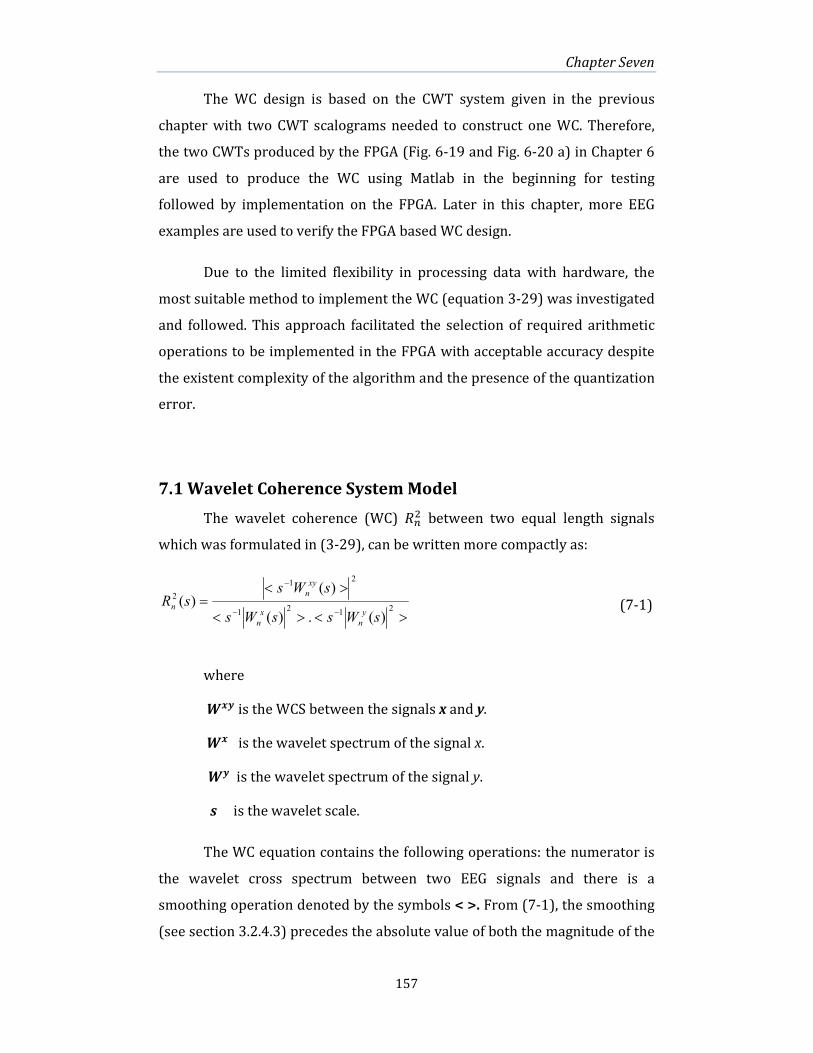
Chapter Seven
157
The WC design is based on the CWT system given in the previous
chapter with two CWT scalograms needed to construct one WC. Therefore,
the two CWTs produced by the FPGA (Fig. 6-19 and Fig. 6-20 a) in Chapter 6
are used to produce the WC using Matlab in the beginning for testing
followed by implementation on the FPGA. Later in this chapter, more EEG
examples are used to verify the FPGA based WC design.
Due to the limited flexibility in processing data with hardware, the
most suitable method to implement the WC (equation 3-29) was investigated
and followed. This approach facilitated the selection of required arithmetic
operations to be implemented in the FPGA with acceptable accuracy despite
the existent complexity of the algorithm and the presence of the quantization
error.
7.1 Wavelet Coherence System Model
The wavelet coherence (WC) �%R between two equal length signals
which was formulated in (3-29), can be written more compactly as:
(7-1)
where
�� is the WCS between the signals x and y.
�� is the wavelet spectrum of the signal x.
� is the wavelet spectrum of the signal y.
s is the wavelet scale.
The WC equation contains the following operations: the numerator is
the wavelet cross spectrum between two EEG signals and there is a
smoothing operation denoted by the symbols < >. From (7-1), the smoothing
(see section 3.2.4.3) precedes the absolute value of both the magnitude of the
><><
><
=−−
−
21
21
21
2
)(.)(
)()(
sWssWs
sWssR
y
n
x
n
xy
n
n
Chapter Seven
158
wavelet cross spectrum and the existent square operation. However, in the
denominator, which holds the auto spectrums for both EEGs used in the
equation, the absolute value (magnitude) and square operation for each auto
spectrum needs to be performed before smoothing. Lastly, the cross
spectrum is divided by the multiplied auto-spectrums to give the wavelet
coherence as a localized correlation coefficient at each time n and scale s [5].
Smoothing is important to obtain a valid measure for the wavelet coherence
and according to Schwarz inequality, the WC (�%R) takes its value between 0
and 1. Without smoothing all of the WC coefficients are trivially equal to one
[5].
When a large collection of brain neurons fire synchronously32, the
measured EEG waveforms from different electrodes on the scalp are similar.
For example, the measured EEG from the electrodes Fz and Cz of the same
oddball trial are shown in Fig. 7-1 (a). The hardware CWTs of these two
signals are in Fig. 7-1 (b) and (c) respectively and are used for the
experiments to generate the WC in this chapter. Despite the trend of
similarity for the EEGs in Fig. 7-1 (a), there are some differences in their CWT
plots, which also belong to the difference in the colour scale of the plots.
There is a similarity in the island (the period 200-300 ms and around 11 Hz),
which reflects the peak in Fig. 7-1 (a) at the same period. However, the ERP
components (620 ms-830 ms) show different power in the scalogram.
32 Synchronicity between several signals does not necessarily imply that there is a physical
connection between the ‘neural circuits’ generating these signals but could also arise from
induction. In addition, two zones could be driven (synchronous) by a common third zone.

Chapter Seven
159
(c)
(b)
(a)
0 100 200 300 400 500 600 700 800 900 1000-20
-10
0
10
20
30
40
50
Time [ms]
Amplitude [uV]
EEG by Fz
EEG by Cz
ERP
Time [ms]
Frequency [Hz]
100 200 300 400 500 600 700 800 900 1000
37
22
15.6
11
7.8
5.5
3.9
2.7
1.95
20
40
60
80
100
120
140
160
Time [ms](a)
Frequency [Hz]
100 200 300 400 500 600 700 800 900 1000
52.6
37.17
26.24
18.58
13.14
9.29
6.57
4.64
3.28
2.32
20
40
60
80
100
120
140
160
180
200
Figure 7-1(a): Two measured EEG waveforms during the Oddball test from the
brain sites Fz & Cz. (b) is the CWT for Fz. (c) is the CWT for Cz.

Chapter Seven
160
7.1.1 Flow Diagram
To detail the WC algorithm and make it applicable to hardware, a flow
diagram is necessary. Such a flow diagram helps to specify the included
mathematical functions and to investigate possible simplification. The flow
diagram in Fig. 7-2 shows the detailed operations in equation 7-1 with
shaded blocks to discern some of these operations.
CWT1 CWT2 CWT1
Load CWT1, CWT2
Compute the WCS
WCS=cwt1. *(conjugate (cwt2))
Square each magnitude
in CWT1, CWT2
Smooth WCS (Real & Imaginary)
Smooth auto-spectrum (1&2)
Square each WCS
magnitude coefficient
Multiply auto-spectrum1
by auto-spectrum2
Divide WCS by Auto-spectrums’
product at each time and scale
Store the wavelet coherence
coefficients in a memory
CORDIC
Square the real and
imaginary components of
each coefficient for WCS
then add them together
SQRT
Square the real and imaginary
components of each coefficient
for CWT1 then add them
together. The same for CWT2
SQRT
CORDIC
CWT2
Figure 7-2: The flow diagram for the WC algorithm (equation 7-1)
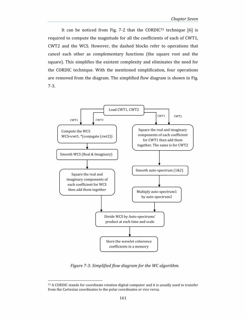
Chapter Seven
161
It can be noticed from Fig. 7-2 that the CORDIC33 technique [6] is
required to compute the magnitude for all the coefficients of each of CWT1,
CWT2 and the WCS. However, the dashed blocks refer to operations that
cancel each other as complementary functions (the square root and the
square). This simplifies the existent complexity and eliminates the need for
the CORDIC technique. With the mentioned simplification, four operations
are removed from the diagram. The simplified flow diagram is shown in Fig.
7-3.
33 A CORDIC stands for coordinate rotation digital computer and it is usually used to transfer
from the Cartesian coordinates to the polar coordinates or vice versa.
CWT1 CWT2 CWT1
Load CWT1, CWT2
Compute the WCS
WCS=cwt1. *(conjugate (cwt2))
Smooth WCS (Real & Imaginary)
Smooth auto-spectrum (1&2)
Multiply auto-spectrum1
by auto-spectrum2
Divide WCS by Auto-spectrums’
product at each time and scale
Store the wavelet coherence
coefficients in a memory
Square the real and
imaginary components of
each coefficient for WCS
then add them together
Square the real and imaginary
components of each coefficient
for CWT1 then add them
together. The same is for CWT2
CWT2
Figure 7-3: Simplified flow diagram for the WC algorithm.
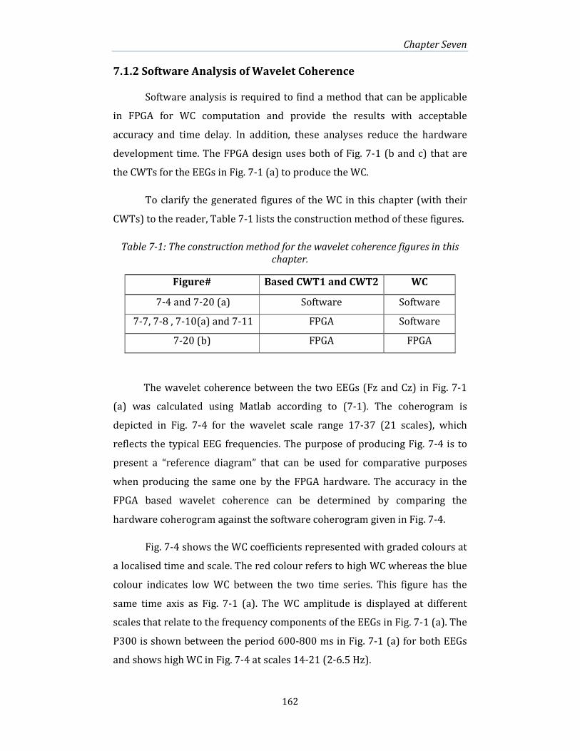
Chapter Seven
162
7.1.2 Software Analysis of Wavelet Coherence
Software analysis is required to find a method that can be applicable
in FPGA for WC computation and provide the results with acceptable
accuracy and time delay. In addition, these analyses reduce the hardware
development time. The FPGA design uses both of Fig. 7-1 (b and c) that are
the CWTs for the EEGs in Fig. 7-1 (a) to produce the WC.
To clarify the generated figures of the WC in this chapter (with their
CWTs) to the reader, Table 7-1 lists the construction method of these figures.
Table 7-1: The construction method for the wavelet coherence figures in this
chapter.
The wavelet coherence between the two EEGs (Fz and Cz) in Fig. 7-1
(a) was calculated using Matlab according to (7-1). The coherogram is
depicted in Fig. 7-4 for the wavelet scale range 17-37 (21 scales), which
reflects the typical EEG frequencies. The purpose of producing Fig. 7-4 is to
present a “reference diagram” that can be used for comparative purposes
when producing the same one by the FPGA hardware. The accuracy in the
FPGA based wavelet coherence can be determined by comparing the
hardware coherogram against the software coherogram given in Fig. 7-4.
Fig. 7-4 shows the WC coefficients represented with graded colours at
a localised time and scale. The red colour refers to high WC whereas the blue
colour indicates low WC between the two time series. This figure has the
same time axis as Fig. 7-1 (a). The WC amplitude is displayed at different
scales that relate to the frequency components of the EEGs in Fig. 7-1 (a). The
P300 is shown between the period 600-800 ms in Fig. 7-1 (a) for both EEGs
and shows high WC in Fig. 7-4 at scales 14-21 (2-6.5 Hz).
Figure# Based CWT1 and CWT2 WC
7-4 and 7-20 (a) Software Software
7-7, 7-8 , 7-10(a) and 7-11 FPGA Software
7-20 (b) FPGA FPGA
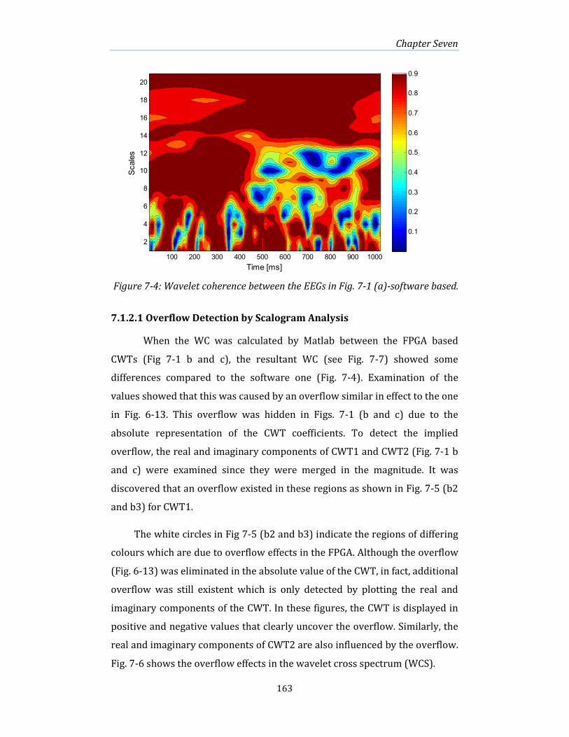
Chapter Seven
163
7.1.2.1 Overflow Detection by Scalogram Analysis
When the WC was calculated by Matlab between the FPGA based
CWTs (Fig 7-1 b and c), the resultant WC (see Fig. 7-7) showed some
differences compared to the software one (Fig. 7-4). Examination of the
values showed that this was caused by an overflow similar in effect to the one
in Fig. 6-13. This overflow was hidden in Figs. 7-1 (b and c) due to the
absolute representation of the CWT coefficients. To detect the implied
overflow, the real and imaginary components of CWT1 and CWT2 (Fig. 7-1 b
and c) were examined since they were merged in the magnitude. It was
discovered that an overflow existed in these regions as shown in Fig. 7-5 (b2
and b3) for CWT1.
The white circles in Fig 7-5 (b2 and b3) indicate the regions of differing
colours which are due to overflow effects in the FPGA. Although the overflow
(Fig. 6-13) was eliminated in the absolute value of the CWT, in fact, additional
overflow was still existent which is only detected by plotting the real and
imaginary components of the CWT. In these figures, the CWT is displayed in
positive and negative values that clearly uncover the overflow. Similarly, the
real and imaginary components of CWT2 are also influenced by the overflow.
Fig. 7-6 shows the overflow effects in the wavelet cross spectrum (WCS).
Time [ms]
Scales
100 200 300 400 500 600 700 800 900 1000
2
4
6
8
10
12
14
16
18
20
0.1
0.2
0.3
0.4
0.5
0.6
0.7
0.8
0.9
Figure 7-4: Wavelet coherence between the EEGs in Fig. 7-1 (a)-software based.

Chapter Seven
164
200 400 600 800 1000
2
4
6
8
10
12
14
16
18
20
20
40
60
80
100
120
140
160
200 400 600 800 1000
2
4
6
8
10
12
14
16
18
20
20
40
60
80
100
120
140
160
Real part
200 400 600 800 1000
2
4
6
8
10
12
14
16
18
20
-150
-100
-50
0
50
100
150Real part
200 400 600 800 1000
2
4
6
8
10
12
14
16
18
20
-150
-100
-50
0
50
100
150
200 400 600 800 1000
2
4
6
8
10
12
14
16
18
20
-150
-100
-50
0
50
100
150
200 400 600 800 1000
2
4
6
8
10
12
14
16
18
20
-150
-100
-50
0
50
100
150
(a1) (b1)
(a2) (b2)
(a3) (b3)
Figure 7-5: (a1, a2&a3) software based CWT1, its real & imaginary components
respectively. (b1, b2&b3) FPGA based CWT1, its real & imaginary components
respectively. The white circle shows the region where the effect of overflow appears.
Sca
le
Sca
le
Sca
le
Time [ms] Time [ms]

Chapter Seven
165
The effect of overflow is noticeable in both components of the WCS in
Fig. 7-6 (a and b) inside the circle and the oval. However, this effect
disappeared in Fig. 7-6 (c), again because the WCS is shown in the absolute
value. Other scalogram plots were also computed that are the smoothed
magnitudes for CWT1 and CWT2, the power of two for the smoothed WCS
and the auto-spectrum where the overflow also appeared in this fashion (not
presented).
Time [ms]
Scales
100 200 300 400 500 600 700 800 900 1000
2
4
6
8
10
12
14
16
18
20
Time [ms]
100 200 300 400 500 600 700 800 900 1000
2
4
6
8
10
12
14
16
18
20
Time [ms]
Scales
100 200 300 400 500 600 700 800 900 1000
2
4
6
8
10
12
14
16
18
20
0.5
1
1.5
2
2.5x 10
4
(a) WCS- Real Component (b) WCS- Imaginary Component
(c) WCS-Magnitude
Figure 7-6: WCS (a) real component (b) imaginary component (c) magnitude.
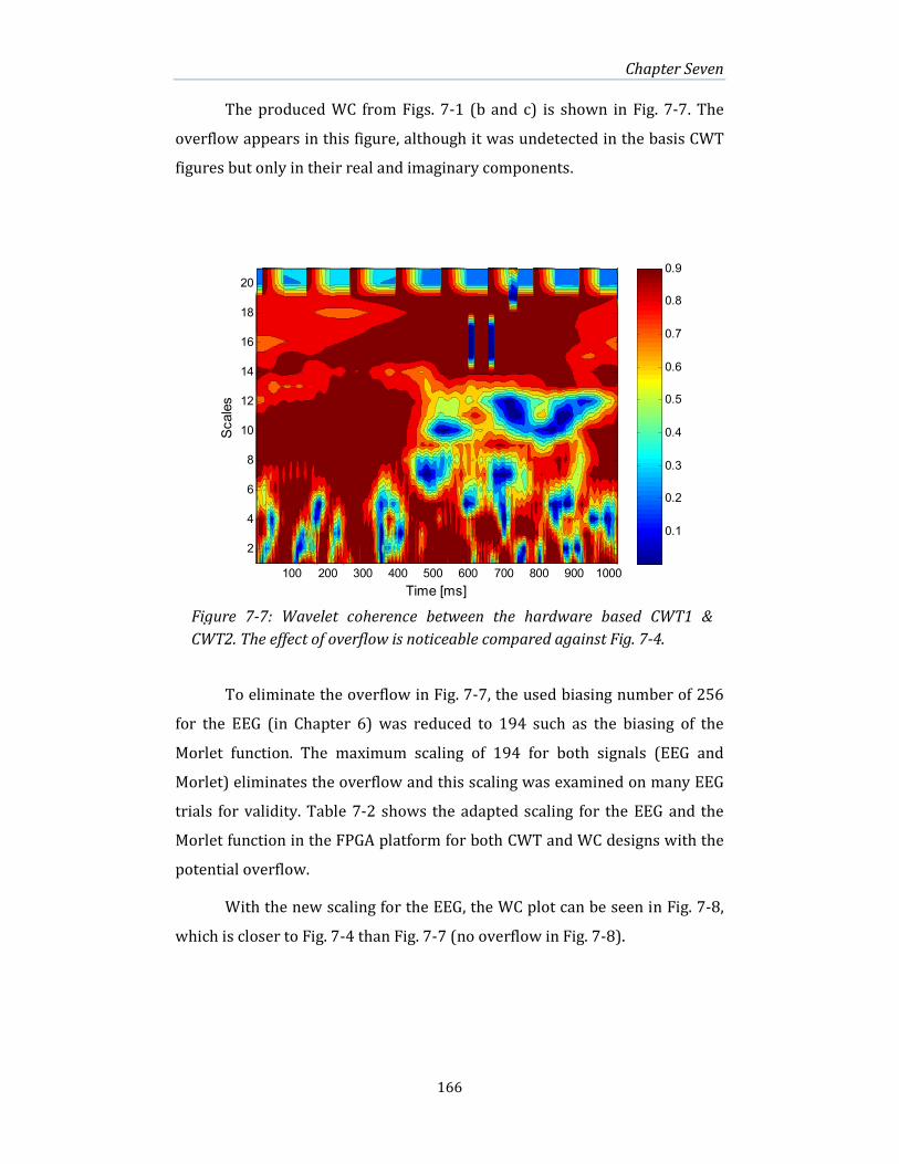
Chapter Seven
166
The produced WC from Figs. 7-1 (b and c) is shown in Fig. 7-7. The
overflow appears in this figure, although it was undetected in the basis CWT
figures but only in their real and imaginary components.
To eliminate the overflow in Fig. 7-7, the used biasing number of 256
for the EEG (in Chapter 6) was reduced to 194 such as the biasing of the
Morlet function. The maximum scaling of 194 for both signals (EEG and
Morlet) eliminates the overflow and this scaling was examined on many EEG
trials for validity. Table 7-2 shows the adapted scaling for the EEG and the
Morlet function in the FPGA platform for both CWT and WC designs with the
potential overflow.
With the new scaling for the EEG, the WC plot can be seen in Fig. 7-8,
which is closer to Fig. 7-4 than Fig. 7-7 (no overflow in Fig. 7-8).
Time [ms]
Scales
100 200 300 400 500 600 700 800 900 1000
2
4
6
8
10
12
14
16
18
20
0.1
0.2
0.3
0.4
0.5
0.6
0.7
0.8
0.9
Figure 7-7: Wavelet coherence between the hardware based CWT1 &
CWT2. The effect of overflow is noticeable compared against Fig. 7-4.
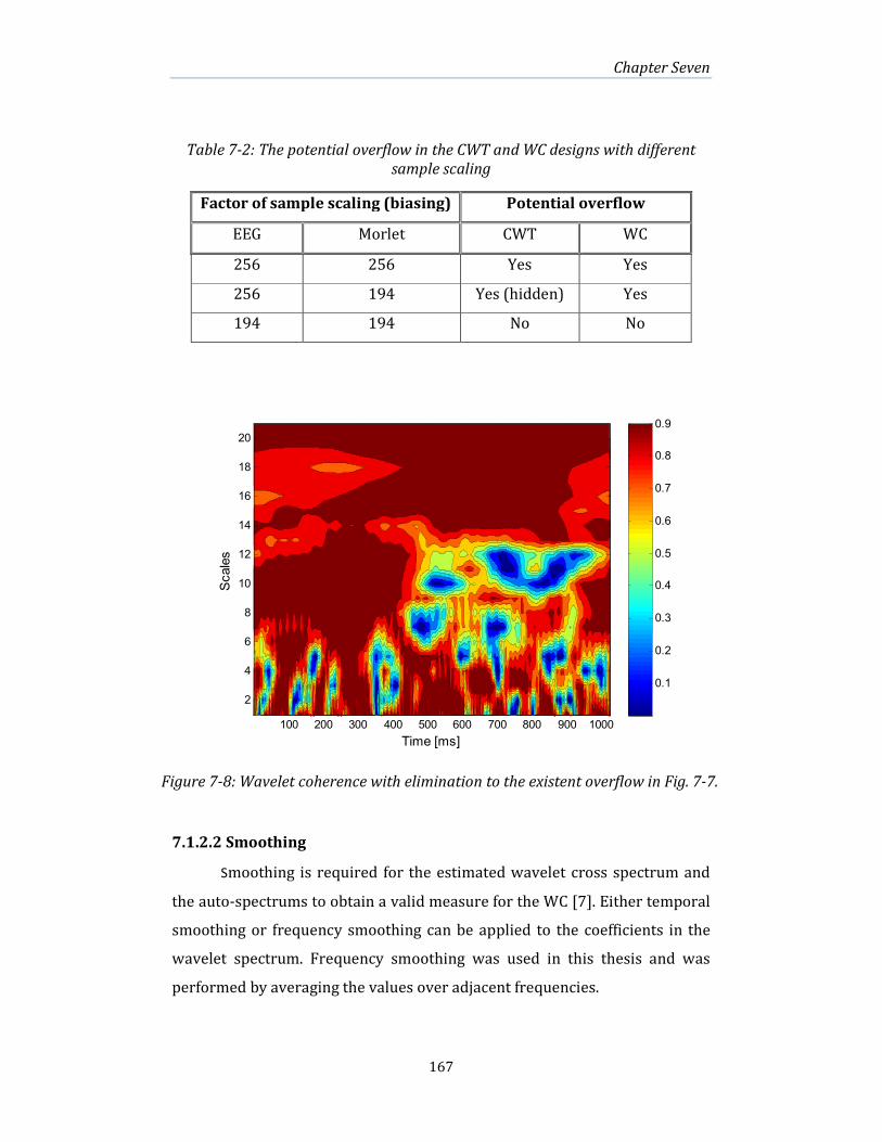
Chapter Seven
167
Table 7-2: The potential overflow in the CWT and WC designs with different
sample scaling
Factor of sample scaling (biasing) Potential overflow
EEG Morlet CWT WC
256 256 Yes Yes
256 194 Yes (hidden) Yes
194 194 No No
7.1.2.2 Smoothing
Smoothing is required for the estimated wavelet cross spectrum and
the auto-spectrums to obtain a valid measure for the WC [7]. Either temporal
smoothing or frequency smoothing can be applied to the coefficients in the
wavelet spectrum. Frequency smoothing was used in this thesis and was
performed by averaging the values over adjacent frequencies.
Time [ms]
Scales
100 200 300 400 500 600 700 800 900 1000
2
4
6
8
10
12
14
16
18
20
0.1
0.2
0.3
0.4
0.5
0.6
0.7
0.8
0.9
Figure 7-8: Wavelet coherence with elimination to the existent overflow in Fig. 7-7.

Chapter Seven
168
Frequency smoothing is adapted from [8] and modified to simplify the
FPGA processing. Frequency smoothing is given by taking the average of the
coefficients over the frequency axis, i.e. if w is the coefficient of wavelet
spectrum matrix of time axis t and scale axis s and W is the smoothed
coefficient, then frequency smoothing can be applied at each time and scale
such that:
[#,G =d(�, 5)5 + d(�, 5 + 1)5 + 1 + d(�, 5 + 2)5 + 2 (7-2)
Equation (7-2) was used to smooth the wavelet auto and cross
spectrums required to produce the WC in Figs. 7-4, 7-7 and
7-8. An example of the impact of frequency smoothing that uses (7-2) can be
seen in Fig. 7-9. Fig. 7-9 (a) shows a wavelet auto-spectrum before smoothing
and the change in the spectrum when smoothing takes place can be seen in
Fig. 7-9 (b). The smoothed coefficients in Fig. 7-9 (b) have fewer colour steps
compared with the coefficients in Fig. 7-9 (a), which is apparent from the
increase in the number of graded colours that reflect these coefficients. From
the FPGA side, as it shows, (7-2) contains addition and division operations.
Addition can be easily implemented in FPGA but the implementation of
division does not seem appropriate especially when there is a remainder
from the operation.
The WC can be estimated in more than one method and there is no
standard method to compute the WC [1]. For the frequency smoothing in (7-
2), it was empirically modified to suit the hardware environment.
The modification was applied for the three division operations existent in
the terms of (7-2), where the divisor numbers (denominators) were chosen
as two or multiples of two which can be easily achieved in hardware with
arithmetic shift right. The modified equation is as follows:
[#,G =d(�, 5)� + d(�, 5 + 1)¾ + d(�, 5 + 2)� (7-3)
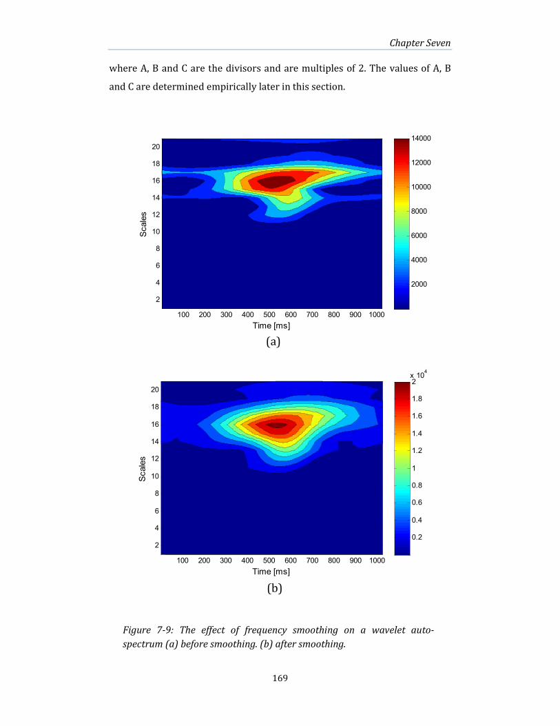
Chapter Seven
169
where A, B and C are the divisors and are multiples of 2. The values of A, B
and C are determined empirically later in this section.
Time [ms](b)
Scales
100 200 300 400 500 600 700 800 900 1000
2
4
6
8
10
12
14
16
18
20
0.2
0.4
0.6
0.8
1
1.2
1.4
1.6
1.8
2x 10
4
Time [ms](a)
Scales
100 200 300 400 500 600 700 800 900 1000
2
4
6
8
10
12
14
16
18
20
2000
4000
6000
8000
10000
12000
14000
Figure 7-9: The effect of frequency smoothing on a wavelet auto-
spectrum (a) before smoothing. (b) after smoothing.
(a)
(b)
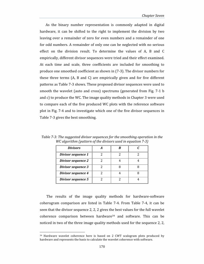
Chapter Seven
170
As the binary number representation is commonly adapted in digital
hardware, it can be shifted to the right to implement the division by two
leaving over a remainder of zero for even numbers and a remainder of one
for odd numbers. A remainder of only one can be neglected with no serious
effect on the division result. To determine the values of A, B and C
empirically, different divisor sequences were tried and their effect examined.
At each time and scale, three coefficients are included for smoothing to
produce one smoothed coefficient as shown in (7-3). The divisor numbers for
these three terms (A, B and C) are empirically given and for five different
patterns as Table 7-3 shows. These proposed divisor sequences were used to
smooth the wavelet (auto and cross) spectrums (generated from Fig. 7-1 b
and c) to produce the WC. The image quality methods in Chapter 3 were used
to compare each of the five produced WC plots with the reference software
plot in Fig. 7-4 and to investigate which one of the five divisor sequences in
Table 7-3 gives the best smoothing.
Table 7-3: The suggested divisor sequences for the smoothing operation in the
WC algorithm (pattern of the divisors used in equation 7-3)
Divisors A B C
Divisor sequence 1 2 2 2
Divisor sequence 2 2 4 4
Divisor sequence 3 2 8 8
Divisor sequence 4 2 4 8
Divisor sequence 5 2 2 4
The results of the image quality methods for hardware-software
coherogram comparison are listed in Table 7-4. From Table 7-4, it can be
seen that the divisor sequence 2, 2, 2 gives the best values for the full wavelet
coherence comparison between hardware34 and software. This can be
noticed in two of the three image quality methods used for the sequence 2, 2,
34 Hardware wavelet coherence here is based on 2 CWT scalogram plots produced by
hardware and represents the basis to calculate the wavelet coherence with software.
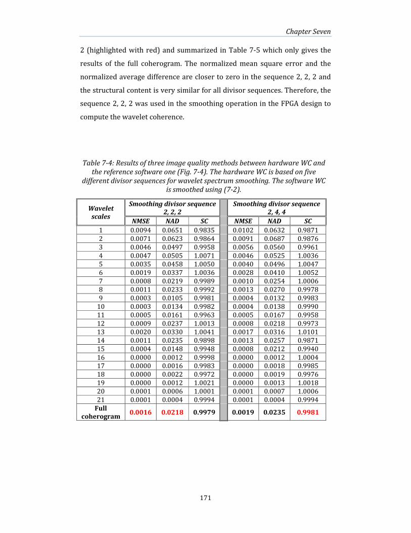
Chapter Seven
171
2 (highlighted with red) and summarized in Table 7-5 which only gives the
results of the full coherogram. The normalized mean square error and the
normalized average difference are closer to zero in the sequence 2, 2, 2 and
the structural content is very similar for all divisor sequences. Therefore, the
sequence 2, 2, 2 was used in the smoothing operation in the FPGA design to
compute the wavelet coherence.
Wavelet
scales
Smoothing divisor sequence
2, 2, 2
Smoothing divisor sequence
2, 4, 4
NMSE NAD SC NMSE NAD SC
1 0.0094 0.0651 0.9835 0.0102 0.0632 0.9871
2 0.0071 0.0623 0.9864 0.0091 0.0687 0.9876
3 0.0046 0.0497 0.9958 0.0056 0.0560 0.9961
4 0.0047 0.0505 1.0071 0.0046 0.0525 1.0036
5 0.0035 0.0458 1.0050 0.0040 0.0496 1.0047
6 0.0019 0.0337 1.0036 0.0028 0.0410 1.0052
7 0.0008 0.0219 0.9989 0.0010 0.0254 1.0006
8 0.0011 0.0233 0.9992 0.0013 0.0270 0.9978
9 0.0003 0.0105 0.9981 0.0004 0.0132 0.9983
10 0.0003 0.0134 0.9982 0.0004 0.0138 0.9990
11 0.0005 0.0161 0.9963 0.0005 0.0167 0.9958
12 0.0009 0.0237 1.0013 0.0008 0.0218 0.9973
13 0.0020 0.0330 1.0041 0.0017 0.0316 1.0101
14 0.0011 0.0235 0.9898 0.0013 0.0257 0.9871
15 0.0004 0.0148 0.9948 0.0008 0.0212 0.9940
16 0.0000 0.0012 0.9998 0.0000 0.0012 1.0004
17 0.0000 0.0016 0.9983 0.0000 0.0018 0.9985
18 0.0000 0.0022 0.9972 0.0000 0.0019 0.9976
19 0.0000 0.0012 1.0021 0.0000 0.0013 1.0018
20 0.0001 0.0006 1.0001 0.0001 0.0007 1.0006
21 0.0001 0.0004 0.9994 0.0001 0.0004 0.9994
Full
coherogram 0.0016 0.0218 0.9979 0.0019 0.0235 0.9981
Table 7-4: Results of three image quality methods between hardware WC and
the reference software one (Fig. 7-4). The hardware WC is based on five
different divisor sequences for wavelet spectrum smoothing. The software WC
is smoothed using (7-2).

Chapter Seven
172
Wavelet
scales
Smoothing divisor
sequence
2, 8, 8
Smoothing divisor sequence
2, 4, 8
NMSE NAD SC NMSE NAD SC
1 0.0087 0.0535 0.9902 0.0102 0.0632 0.9871
2 0.0107 0.0699 0.9891 0.0098 0.0688 0.9853
3 0.0060 0.0588 0.9938 0.0054 0.0549 0.9918
4 0.0043 0.0511 0.9989 0.0041 0.0494 1.0001
5 0.0042 0.0513 1.0037 0.0044 0.0513 1.0056
6 0.0039 0.0483 1.0070 0.0031 0.0433 1.0067
7 0.0012 0.0277 1.0020 0.0011 0.0263 1.0019
8 0.0013 0.0273 0.9964 0.0011 0.0253 0.9966
9 0.0005 0.0157 0.9987 0.0005 0.0144 0.9992
10 0.0004 0.0147 1.0000 0.0004 0.0139 0.9996
11 0.0005 0.0160 0.9959 0.0005 0.0159 0.9967
12 0.0007 0.0188 0.9935 0.0006 0.0182 0.9960
13 0.0018 0.0319 1.0170 0.0016 0.0293 1.0143
14 0.0015 0.0280 0.9824 0.0030 0.0372 0.9814
15 0.0011 0.0262 0.9949 0.0008 0.0229 0.9934
16 0.0000 0.0014 1.0008 0.0000 0.0014 1.0009
17 0.0001 0.0023 0.9989 0.0001 0.0018 0.9986
18 0.0000 0.0015 0.9982 0.0000 0.0018 0.9978
19 0.0000 0.0015 1.0009 0.0000 0.0015 1.0010
20 0.0000 0.0009 1.0011 0.0000 0.0008 1.0010
21 0.0001 0.0004 0.9994 0.0001 0.0003 0.9995
Full
coherogram 0.0020 0.0240 0.9981 0.0020 0.0239 0.9976
Table 7-4: Continued from Table 7-4 on previous page

Chapter Seven
173
Table 7-4: Continued
Table 7-5: Divisor sequence results over full coherogram examined with three
image quality methods.
Wavelet Scales Smoothing divisor sequence 2, 2, 4
NMSE NAD SC
1 0.0094 0.0651 0.9835
2 0.0079 0.0651 0.9835
3 0.0048 0.0504 0.9924
4 0.0045 0.0497 1.0045
5 0.0042 0.0499 1.0062
6 0.0022 0.0367 1.0049
7 0.0009 0.0237 1.0006
8 0.0011 0.0243 0.9980
9 0.0003 0.0117 0.9990
10 0.0003 0.0126 0.9987
11 0.0005 0.0156 0.9967
12 0.0005 0.0184 0.9992
13 0.0015 0.0290 1.0072
14 0.0028 0.0355 0.9869
15 0.0005 0.0162 0.9941
16 0.0000 0.0014 1.0005
17 0.0000 0.0015 0.9984
18 0.0000 0.0023 0.9972
19 0.0000 0.0013 1.0018
20 0.0000 0.0006 1.0005
21 0.0001 0.0003 0.9995
Full
coherogram 0.0017 0.0225 0.9976
Divisor Sequence NMSE NAD SC
2, 2, 2 0.0016 0.0218 0.9979
2, 4, 4 0.0019 0.0235 0.9981
2, 8, 8 0.0020 0.0240 0.9981
2, 4, 8 0.0020 0.0239 0.9976
2, 2, 4 0.0017 0.0225 0.9976
Standard Measures 0 0 1

Chapter Seven
174
7.1.2.3 Word Length Selection
The selection of the appropriate word length for WC computation in
FPGA is necessary as a trade-off between the required accuracy and the
occupied FPGA-gate array. The inputs to the wavelet coherence equation are
CWT1 and CWT2 produced by hardware and passed through several
processes that add further quantization error on implementing the rest of the
WC algorithm following the CWTs. Therefore, a suitable word length is
required at each stage to extract the FPGA based WC with maximum
accuracy.
As the CWT returns a 16-bit sample, extending the word length to
more than 16-bits can be applied in the WC design with no concerns since the
FFT core is not needed at this stage. The following word lengths were chosen
to test the accuracy of the presented WC and to select the word length that
gives the best trade-off between the metrics of accuracy and FPGA resources.
The word lengths chosen to test were 16, 32 and 64 bits. These word lengths
were used to represent the variables of equation 7-1 and to construct the WC
based on these lengths. The test of the WC using these word lengths was
performed in Matlab before implementing the chosen word length on the
FPGA. It is worthwhile to mention that the wavelet coherence35 range
between 0-1 cannot be represented in single fixed-point integer value.
However, it can be represented in two colours only: red for 1 and blue for 0,
despite the fact that the initial entries to the WC equation are represented in
16 or 32 or even 64 bits. This problem occurred when the WCS divided by the
auto-spectrum as a hexadecimal number36. Therefore, to give the WC values
between zero and one in graded colours, the WCS was multiplied by a factor
before dividing it by the auto-spectrum. This factor can be, for example, 8 or
16, which reflects the number of colours in the coherogram. This expands the
range from 0-1 to 0-8 etc. (see the colour bars in Fig. 7-10). This method is
followed to help in selecting the appropriate number of colours in the
coherogram for the WC design as shown in Fig. 7-10.
35
The tendency to either 0 or 1 for the WC depends on the approximation of the WC value. 36 The WCS is always less or equal to the auto-spectrum. For example, the division of 7hex by F
results in 0 and the division of F by F gives 1 for fixed point integers.
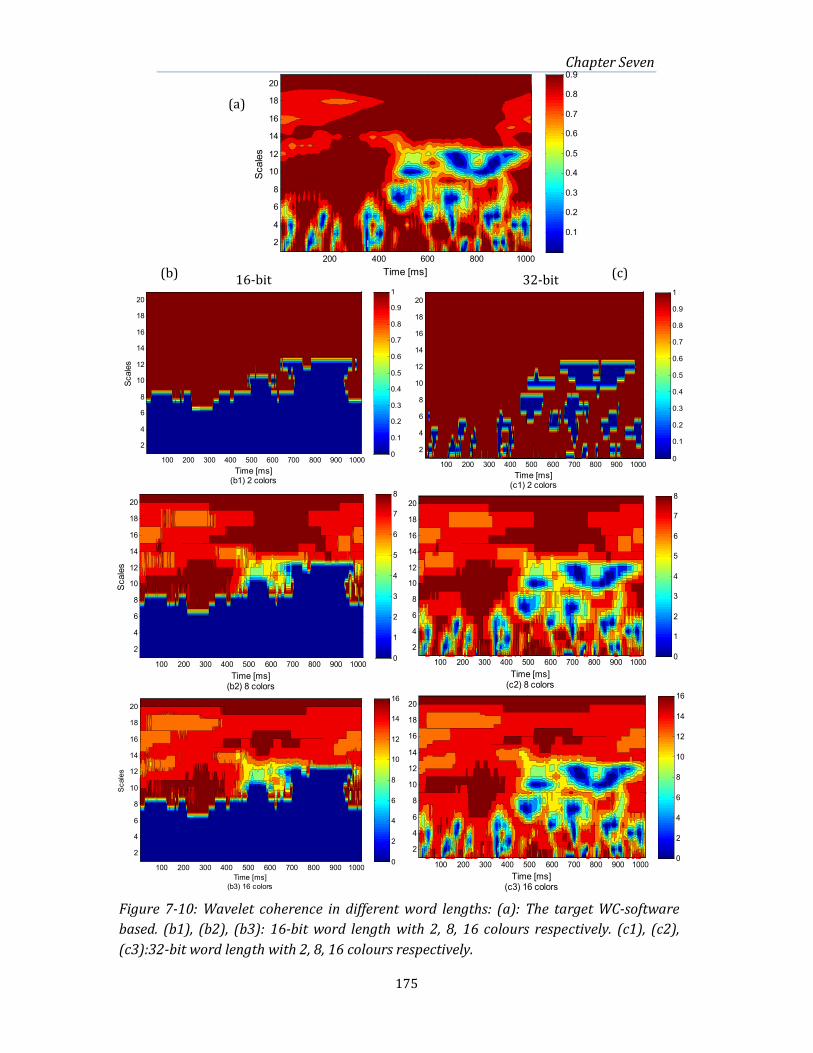
Chapter Seven
175
Time [ms](b1) 2 colors
Scales
100 200 300 400 500 600 700 800 900 1000
2
4
6
8
10
12
14
16
18
20
0
0.1
0.2
0.3
0.4
0.5
0.6
0.7
0.8
0.9
1
Time [ms](c1) 2 colors
100 200 300 400 500 600 700 800 900 1000
2
4
6
8
10
12
14
16
18
20
0
0.1
0.2
0.3
0.4
0.5
0.6
0.7
0.8
0.9
1
Time [ms](b2) 8 colors
Scales
100 200 300 400 500 600 700 800 900 1000
2
4
6
8
10
12
14
16
18
20
0
1
2
3
4
5
6
7
8
Time [ms](c2) 8 colors
100 200 300 400 500 600 700 800 900 1000
2
4
6
8
10
12
14
16
18
20
0
1
2
3
4
5
6
7
8
Time [ms]
(b3) 16 colors
Scales
100 200 300 400 500 600 700 800 900 1000
2
4
6
8
10
12
14
16
18
20
0
2
4
6
8
10
12
14
16
Time [ms](c3) 16 colors
Scales
100 200 300 400 500 600 700 800 900 1000
2
4
6
8
10
12
14
16
18
20
0
2
4
6
8
10
12
14
16
Figure 7-10: Wavelet coherence in different word lengths: (a): The target WC-software
based. (b1), (b2), (b3): 16-bit word length with 2, 8, 16 colours respectively. (c1), (c2),
(c3):32-bit word length with 2, 8, 16 colours respectively.
Time [ms](a)
Scales
200 400 600 800 1000
2
4
6
8
10
12
14
16
18
20
0.1
0.2
0.3
0.4
0.5
0.6
0.7
0.8
0.9
16-bit 32-bit
(a)
(b) (c)

Chapter Seven
176
In Fig. 7-10, several coherogram plots were calculated and the difference
belongs to the colour bar with the maximums of 1, 8 and 16. Fig. 7-10(a) is
the software reference one. In (b1, b2 and b3), 16-bit two’s complement
integers are used to develop the WC represented with two colours in (b1)
and (c1), eight colours in (b2) and (c2), and 16 colours in (b3) and (c3) as the
colour bar indicates. Even when the number of colours is increased up to 16
in (b3), the word length of only 16 bits shows insufficient details.
The WC-32 bit word length in Fig. 7-10(c1, c2 and c3) shows much
better improvement to the coherogram. In Fig. 7-10 (c1) more details can be
seen but the loss of graded colours hides the values of the WC greater than
zero and less than one. When the number of colours increased to eight and
16, as in Fig. 7-10 (c2) and Fig 7-10 (c3) respectively, the coherogram details
appear. Further coherogram plots were made with a 64-bit word length for
the calculation of (7-1) which gave the same result as the case of the 32-bit.
When the number of colours was increased in the plot to 32 or 64, some
noisy features started to appear in the WC as Fig. 7-11 shows (32-bit with 64
colours). Therefore, the 32-bit was chosen with 16 graded colours (Fig. 7-10
c3) to be adapted in the FPGA as it gives the closer representation to Fig. 7-
10(a). The subjective inspection of these figures was sufficient to choose the
most suitable one and there was no need to apply objective measures.
Time [ms]
Scales
100 200 300 400 500 600 700 800 900 1000
2
4
6
8
10
12
14
16
18
20
0
10
20
30
40
50
60
Figure 7-11: Wavelet coherence: noisy features start to appear when the number
of graded colours increased to 64 (compared to Fig. 7-10 a).
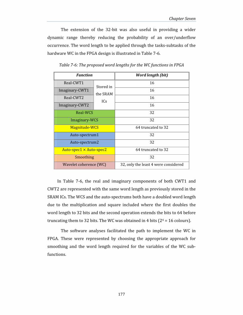
Chapter Seven
177
The extension of the 32-bit was also useful in providing a wider
dynamic range thereby reducing the probability of an over/underflow
occurrence. The word length to be applied through the tasks-subtasks of the
hardware WC in the FPGA design is illustrated in Table 7-6.
Table 7-6: The proposed word lengths for the WC functions in FPGA
Function Word length (bit)
Real-CWT1 Stored in
the SRAM
ICs
16
Imaginary-CWT1 16
Real-CWT2 16
Imaginary-CWT2 16
Real-WCS 32
Imaginary-WCS 32
Magnitude-WCS 64 truncated to 32
Auto-spectrum1 32
Auto-spectrum2 32
Auto-spec1 × Auto-spec2 64 truncated to 32
Smoothing 32
Wavelet coherence (WC) 32, only the least 4 were considered
In Table 7-6, the real and imaginary components of both CWT1 and
CWT2 are represented with the same word length as previously stored in the
SRAM ICs. The WCS and the auto-spectrums both have a doubled word length
due to the multiplication and square included where the first doubles the
word length to 32 bits and the second operation extends the bits to 64 before
truncating them to 32 bits. The WC was obtained in 4 bits (24 = 16 colours).
The software analyses facilitated the path to implement the WC in
FPGA. These were represented by choosing the appropriate approach for
smoothing and the word length required for the variables of the WC sub-
functions.

Chapter Seven
178
7.2 FPGA Implementation of the WC
This section presents the FPGA implementation for the process given
in Fig. 7-3 to produce the WC. This process requires a memory map (RAM) to
read data and store results. The memory map for the WC process is shown in
Table 7-7. This memory map is represented by the two SRAMs (each 256K ×16-bits) where the CWT coefficients were stored in advance as shown in
the table. The allocated locations to store the WC are also indicated. Only the
lower 16 bits of the WC were stored in the SRAM, although the least four bits
were sent to the PC. From Table 7-7, it can be seen that the allocated
locations for the WC are only 19K which represents the coherogram. This is
because the wavelet coefficients at scale 1 and scale 21 were omitted to
facilitate the smoothing operation by the FPGA and the rest of the 19 scales
were considered.
The WC design starts processing the real and imaginary CWT
components in the two SRAMs to produce the coherogram.
Table 7-7: The memory map for the process of wavelet coherence
The location of the SRAM IC with the CWT design and WC design in
the FPGA is shown in Fig. 7-12. The CWT design calculates the wavelet
coefficients for two EEG signals and stores the results in the SRAMs. The WC
design fetches these coefficients from the SRAMs and calculates the WC. The
WC values were stored in the SRAM to be sent to the PC and also used for
biofeedback as later presented in this chapter. It is worthwhile to mention
SRAM0 address
(hexadecimal)
Data size (word:
2 bytes) Data stored
0-53FF 21 K CWT1-real component
5400-A7FF 21 K CWT2-real component
A800-F3FF 19 K WC-16 least significant bits
SRAM1 address
(hexadecimal) Data size Data stored
0-53FF 21 K CWT1-imaginary component
5400-A7FF 21 K CWT2-imaginary component

Chapter Seven
179
that the CWT and the WC were implemented at different times due to FPGA
resource limitations, however, the CWT coefficients were kept in the SRAM
ICs during design exchange.
The detailed memory map for the WC design is in Fig. 7-13 which
shows the storage locations of the real and imaginary components of CWT1
and CWT2-scale based. .
7.2.1 Design Operation
To implement the wavelet coherence on the FPGA, the flow diagram in
Fig. 7-3 was followed starting with the loading of the real and imaginary
components of CWT1 and CWT2. As presented in section 7.1.2, these values
were examined by software for calculating the WC in order to prepare for the
FPGA implementation. The algorithm was implemented in VHDL. To calculate
the WCS, two complex multipliers need to be involved. By considering the
real component as (re) and the imaginary component as (im) for each of
CWT1 and CWT2, the real and imaginary components of the WCS were
calculated as follows:
B FPGA
B
A
A- CWT coefficients for 2 EEG signals.
B- The WC coefficients
CWT
WC
EEGs input
buffer
Wavelet function
input buffer
SRAM
ICs
Figure 7-12: The CWT design and the WC design in the FPGA with the SRAM
ICs used for storing results.
Biofeedback
design

Chapter Seven
180
SRAM0
SRAM1
00 0000 Scale 1
00 0000 Scale 1
00 0001 00 0001
…… ……
00 03FF 00 03FF
00 0400
Scale 2
00 0400
Scale 2
00 0401 00 0401
………. ……….
00 07FF 00 07FF
00 0800
Scale 3
00 0800
Scale 3
00 0801 00 0801
……… ………
00 0BFF 00 0BFF
…….
…………..
…….
………….. ……… ………
……….. ………..
………… …………
00 5000
Scale 21
00 5000
Scale 21 00 5001 00 5001
…………… ……………
00 53FF 00 53FF
00 5400
Scale 1
00 5400
Scale 1 00 5401 00 5401
……….. ………..
00 57FF 00 57FF
00 5800
Scale 2
00 5800
Scale 2 00 5801 00 5801
………….. …………..
00 5BFF 00 5BFF
00 5C00
Scale 3
00 5C00
Scale 3 00 5C01 00 5C01
………… …………
00 5FFF 00 5FFF
………
……………….
………
………………. ………….. …………..
…………… ……………
……………. …………….
00 A400
Scale 21
00 A400
Scale 21 00 A401 00 A401
………… …………
00 A7FF 00 A7FF
Real component-CWT1 Imaginary component-CWT1
Real component-CWT2 Imaginary component CWT2
Figure 7-13: The storage locations of CWT1 & CWT2 in the SRAM ICs

Chapter Seven
181
[��ª� = (�[-1ª� × �[-2ª�) − (�[-1�I × (7b�(�[-2�I)+¿1¿)) (7-4)
[���I = (�[-1ª� × (7b�(�[-2�I)+¿1¿)) + (�[-1�I × �[-2ª�) (7-5)
Equations 7-4 and 7-5 were performed using two’s complement
arithmetic. This was needed to compute the conjugate of the number which
requires reversing the sign of the imaginary component of CWT2 since [�� = �[-1 × �b74(�[-2). To find the auto-spectrum for each of CWT1 and CWT2, two square
operations and one addition are needed for each spectrum:
��1 = (�[-1ª� × �[-1ª�) + (�[-1�I × �[-1�I) (7-6)
��2 = (�[-2ª� × �[-2ª�) + (�[-2�I × �[-2�I) (7-7)
The schematic diagram to calculate the WCS and the auto-spectrums
is shown in Fig. 7-14. It can be seen from the figure that eight multipliers are
involved in the computation process. To compute the two’s complement, two
identical circuits are used since the real and imaginary components
multiplications are performed simultaneously.
The implementation of smoothing in VHDL according to divisor
sequence 1 in Table 7-3 is the most complex operation in the design. This is
due to the required switching over of SRAM addresses to fetch the desired
CWT coefficients. This switching method was non-sequential and performed
every clock pulse going through 4 × 21K addresses where no more than one
location in each SRAM can be accessed at a time. The wavelet coefficients for
individual scales were stored in SRAM0 and SRAM1 as shown in Fig. 7-13.
This figure is necessary to explain the address switching required for
smoothing the CWTs and their spectrums.
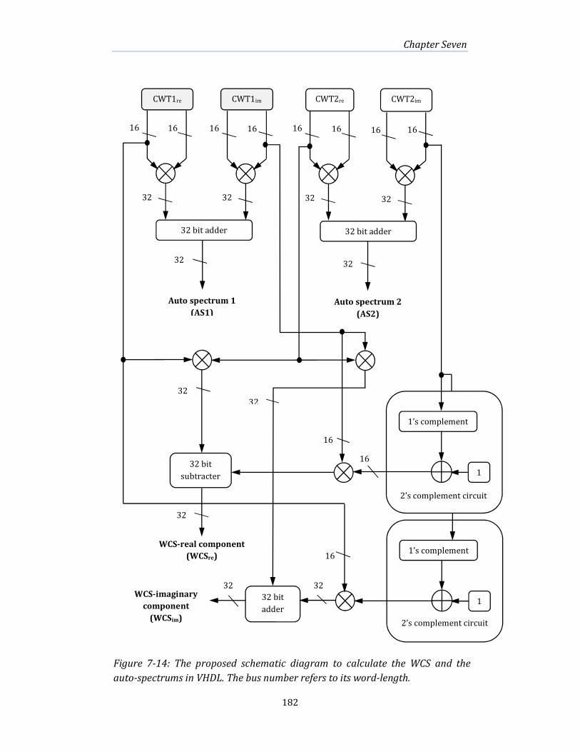
Chapter Seven
182
WCS-real component
(WCSre)
16 16 16
32
16
CWT1re CWT2re CWT1im CWT2im
32
16
32
16
32 bit adder
Auto spectrum 1
(AS1)
32
16
32 32
32
32
32
32
32
16
16
32 bit adder
Auto spectrum 2
(AS2)
1’s complement
1
2’s complement circuit
32 bit
subtracter
1’s complement
1 32 bit
adder
2’s complement circuit
WCS-imaginary
component
(WCSim)
16
Figure 7-14: The proposed schematic diagram to calculate the WCS and the
auto-spectrums in VHDL. The bus number refers to its word-length.
16
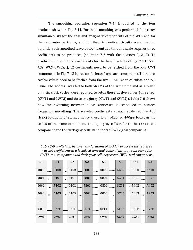
Chapter Seven
183
The smoothing operation (equation 7-3) is applied to the four
products shown in Fig. 7-14. For that, smoothing was performed four times
simultaneously for the real and imaginary components of the WCS and for
the two auto-spectrums, and for that, 4 identical circuits were used in
parallel. Each smoothed wavelet coefficient at a time and scale requires three
coefficients to be produced (equation 7-3 with the divisors 2, 2, 2). To
produce four smoothed coefficients for the four products of Fig. 7-14 (AS1,
AS2, WCSre, WCSim), 12 coefficients need to be fetched from the four CWT
components in Fig. 7-13 (three coefficients from each component). Therefore,
twelve values need to be fetched from the two SRAM ICs to calculate one WC
value. The address was fed to both SRAMs at the same time and as a result
only six clock cycles were required to fetch these twelve values (three real
(CWT1 and CWT2) and three imaginary (CWT1 and CWT2)). Table 7-8 shows
how the switching between SRAM addresses is scheduled to achieve
frequency smoothing. The wavelet coefficients at each scale require 400
(HEX) locations of storage hence there is an offset of 400HEX between the
scales of the same component. The light-gray cells refer to the CWT1-real
component and the dark-gray cells stand for the CWT2_real component.
Table 7-8: Switching between the locations of SRAM0 to access the required
wavelet coefficients at a localized time and scale; light-gray cells stand for
CWT1-real component and dark-gray cells represent CWT2-real component.
S1 S1 S2 S2 S3 S3 S21 S21
0000 5400 0400 5800 0800 5C00 … 5000 A400
0001 5401 0401 5801 0801 5C01 … 5001 A401
0002 5402 0402 5802 0802 5C02 … 5002 A402
0003 5403 0403 5803 0803 5C03 … 5003 A403
…… … …… … … … …… … …… … … … …. ….
03FF 57FF 07FF 5BFF 0BFF 5FFF … 53FF A7FF
Cwt1 Cwt2 Cwt1 Cwt2 Cwt1 Cwt2 Cwt1 Cwt2

Chapter Seven
184
In order to explain Table 7-8, Fig. 7-15 shows the location of the CWT1
(real) coefficients in the wavelet plane and how the smoothing of these
coefficients was applied.
In Fig. 7-15, each of the three smoothed coefficients are one-colour
circled to reflect the addressing schedule in Table 7-8. This table shows the
switching between the SRAM addresses, which is followed in both SRAM0
and SRAM1 at the same time. The first 6 fetched coefficients are at addresses
0000, 5400, 0400, 5800, 0800, 5C00; which are entered into the WC
processor. However, fetching CWT1-real from SRAM0 followed the address
sequence 0000, 0400, 0800, 0001, 0401, 0801 etc. and fetching CWT2-real
from SRAM0 followed the address sequence 5400, 5800, 5C00, 5401, 5801,
5C01 etc. The interleaving in the fetching procedure was necessary to
provide the coefficients simultaneously since they are needed at the same
time to calculate the WC coefficients. For that, to produce one smoothed
coefficient, the values at locations 0000, 0400 and 0800 are needed together
(see Fig. 7-15).
t1 t2 …. t1024
Scale 1 0000 0001 …. 03FF
Scale 2 0400 0401 ….. 07FF
Scale 3 0800 0801 ….. 0BFF
……. ….
Scale 21 5000 5001 ….. 53FF
Figure 7-15: The locations of CWT1 (real) in the wavelet plane indicating the
coefficients that smoothed together. The black, blue and yellow circles
represent the smoothed coefficients at time index t1, t2 and t1024 respectively.
Chapter Seven
185
Four smoothing operations are processed in parallel. At column bases
in Table 7-8, the first light-gray column is the CWT1-real coefficients at scale
1 and the second light-gray column is the CWT1-real coefficients at scale 2
and so on. Table 7-8 is continuous until the wavelet coefficient at the last
occupied location A7FF has been fetched. The same addressing schedule is
applied for SRAM1. See also Fig. 7-13 for further clarification.
The timing simulation for SRAM0 address switching to fetch the real
component of CWT1 can be seen in Fig. 7-16. In this timing figure, 21 internal
signals are allocated to generate the initial addresses for the smoothing
operation, although only eight are shown (start_addr1 to start_addr8).
Three of these addresses are always active at any time to generate the light-
gray sequence in Table 7-8. The generated address sequence can be followed
at the output green signal “address” in Fig. 7-16. The timing also shows how
smoothing is performed. An arithmetic shift right with one bit is performed
to the 16-bit input re_dat1. The first 16 bits “F210” are changed in the signal
coef1 to “F908“ as a result of the shift, which means dividing the value by two
followed by transferring coef1 to coef2 which in turn is transferred to coef3.
When the counter cntr counts three, the three red values (coef1, coef2 and
coef3) are added together to produce the first coefficient of smoothing in the
next clock cycle (2000h+1100h+F908h= 2A08h) which can be seen in the
output signal re_out and so on.
SRAM0 addressing is actually performed to fetch the real components
of CWT1 and CWT2 (Table 7-8), but the timing simulation in Fig. 7-16 shows
the addressing method for CWT1 (real) only for simplicity. The method used
for CWT2 (real) and for the imaginary terms is exactly the same method but
performed on different memory banks. The timing diagram verifies the
change in the values of the signals listed in the simulation according to the
clock pulses given. Hence, it reflects the operation of the WC design.
Fig. 7-17 shows the block diagram for the proposed smoothing circuit
in the FPGA. It is clear from Fig. 7-17 that the arithmetic shift right is
performed to divide each of the four outputs of Fig. 7-14 by two.

Chapter Seven
186
Fig
ure
7-1
6:
Th
e ti
min
g s
imu
lati
on
fo
r th
e a
dd
ress
sw
itch
ing
met
ho
d o
f S
RA
M0
to
im
ple
men
t th
e s
mo
oth
ing
fu
nct
ion

Chapter Seven
187
Serial in/parallel out
32 bit
32 bit 32 bit 32 bit
32-bit
input
32-bit Smoothed
output
Arithmetic Shift Right
32-bit
register
32-bit
register
32-bit
register
32-bit adder
32-bit
register
Clock
source
Enable
Figure 7-17: The proposed block diagram for the 32-bit smoothing circuit as
an implementation to the equation above the figure. The 32-bit smoothed
output is only produced when an enable pulse is given.
Read
number
Divide
by 2
32 bit
[#,G = d(�, 5)2 + d(�, 5 + 1)2 + d(�, 5 + 2)2

Chapter Seven
188
Three values (32-bits each) from the memory bank are entered
sequentially to the smoothing circuit in Fig. 7-17. Following the division
process, which is performed by the right shift of one bit, these values are
added together using a 32-bit adder and the final result is produced when the
enable pulse of the output register is given. The output represents the terms
of (7-3) added together using the divisor sequences 2, 2, 2. Four replicas of
this smoothing circuit are used to smooth each of the four outputs in Fig. 7-
14 simultaneously.
To calculate one value for the wavelet coherence at a time and scale,
three values are required from each of the four components of CWT1 (real
and imaginary) and CWT2 (real and imaginary). Therefore, twelve values are
fetched (six from each SRAM). The wavelet coherence coefficients are stored
in SRAM0 starting from the location “A800”, for the 16 lower order bits37.
The timing simulation for the fetch operation, the WCS calculation, the
four smoothing operations and auto-spectrums can be seen in Fig. 7-18. This
figure only shows the computations of the main mathematical operations to
produce the WCS and auto-spectrums required for the wavelet coherence. No
signals are presented. Following the rst (reset) and clk (clock) signals, the
green sections are the CWT1 and CWT2 components that are synchronized
by putting CWT1 (real and imaginary components) in a one clock register
delay since CWT1 components precede CWT2 components with one clock
cycle. The auto and cross spectrum waveforms are then produced. Each one
of the four smoothing operations smth1, smth2, smth3 and smth4 in Fig. 7-
18 has three sub-signals and a counter. The counter–after-initialization-
counts two, three and at four, the addition is performed. This allows three
values to be involved for smoothing then the counter starts counting from
two again. The last two signals (in red) are the WCS and the auto-spectrum
truncated to 32 bits. This timing simulation is used to verify the operation of
the WC algorithm for a small amount of data. It also shows the expected
latency to produce the WC coefficients.
37 No need for the higher 16 bits of the WC. Even for the lower 16 bits, only the four least bits
are needed to construct a WC based on 16 colours as proposed in section 7.1.2.3.

Chapter Seven
189
As the timing simulation is used for verifying operations for the design
tasks, not all the generated timing diagrams are presented.
Fig
ure
7-1
8:
Th
e ti
min
g s
imu
lati
on
fo
r th
e m
ain
fu
nct
ion
s to
pro
du
ce t
he
wa
vele
t co
he
ren
ce.

Chapter Seven
190
7.2.2 The wavelet Coherence Processor
The designed WC processor is shown in Fig. 7-19 with the name, type
and description of I/O ports given in Table 7-9. The VHDL code for the
wavelet coherence processor is provided in Appendix C of this thesis.
Table 7-9: Name, type and description for the ports of the WC processor
Port Name Type Description
clk Input Clock signal
im[15..0] Input The CWT imaginary components fetched from SRAM1
re[15..0] Input The CWT real components fetched from SRAM0
rst Input Reset signal
address[17..0] Output The SRAM0 and SRAM1 address bus
counter[19..0] Output Address counter
oe Output Read enable for the SRAM ICs
scl_gg[4..0] Output Wavelet scale counter
trig_SLR Output Status signal to the serial port for WC data transfer
wc[31..0] Output The produced wavelet coherence in 32 bits
we Output Write enable for the SRAM ICs
Figure 7-19: The VHDL-based wavelet coherence processor in the design sheet.
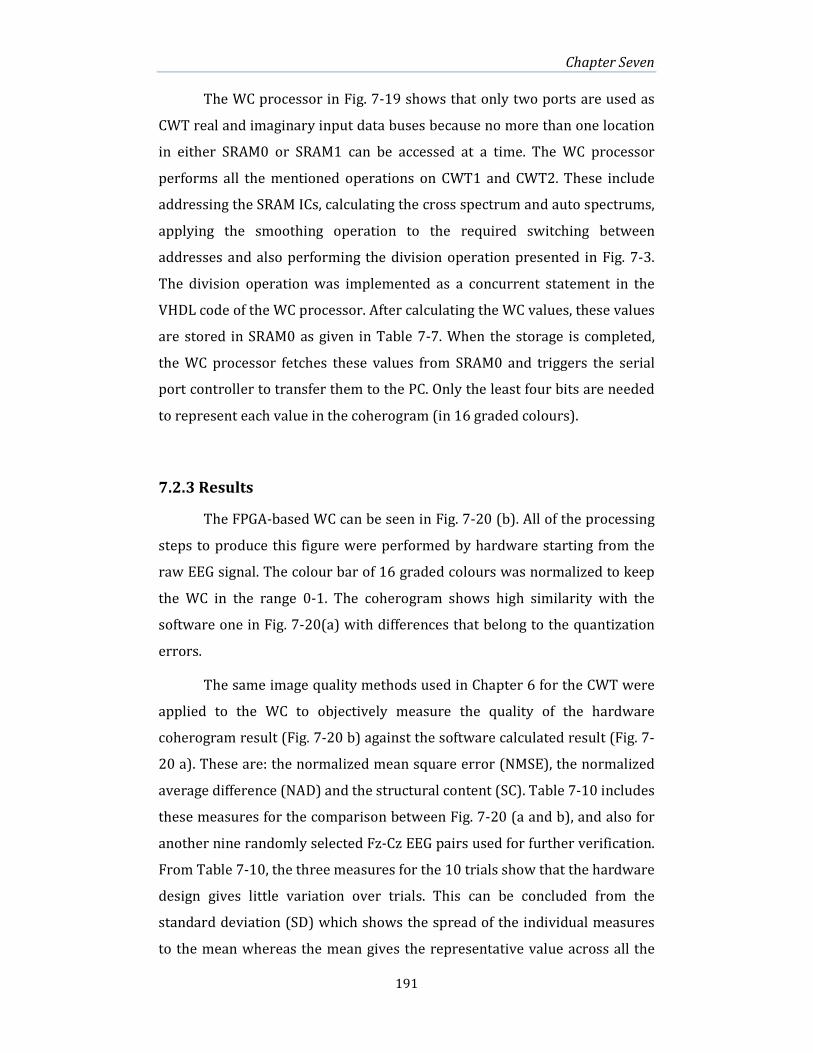
Chapter Seven
191
The WC processor in Fig. 7-19 shows that only two ports are used as
CWT real and imaginary input data buses because no more than one location
in either SRAM0 or SRAM1 can be accessed at a time. The WC processor
performs all the mentioned operations on CWT1 and CWT2. These include
addressing the SRAM ICs, calculating the cross spectrum and auto spectrums,
applying the smoothing operation to the required switching between
addresses and also performing the division operation presented in Fig. 7-3.
The division operation was implemented as a concurrent statement in the
VHDL code of the WC processor. After calculating the WC values, these values
are stored in SRAM0 as given in Table 7-7. When the storage is completed,
the WC processor fetches these values from SRAM0 and triggers the serial
port controller to transfer them to the PC. Only the least four bits are needed
to represent each value in the coherogram (in 16 graded colours).
7.2.3 Results
The FPGA-based WC can be seen in Fig. 7-20 (b). All of the processing
steps to produce this figure were performed by hardware starting from the
raw EEG signal. The colour bar of 16 graded colours was normalized to keep
the WC in the range 0-1. The coherogram shows high similarity with the
software one in Fig. 7-20(a) with differences that belong to the quantization
errors.
The same image quality methods used in Chapter 6 for the CWT were
applied to the WC to objectively measure the quality of the hardware
coherogram result (Fig. 7-20 b) against the software calculated result (Fig. 7-
20 a). These are: the normalized mean square error (NMSE), the normalized
average difference (NAD) and the structural content (SC). Table 7-10 includes
these measures for the comparison between Fig. 7-20 (a and b), and also for
another nine randomly selected Fz-Cz EEG pairs used for further verification.
From Table 7-10, the three measures for the 10 trials show that the hardware
design gives little variation over trials. This can be concluded from the
standard deviation (SD) which shows the spread of the individual measures
to the mean whereas the mean gives the representative value across all the

Chapter Seven
192
trials. It can be seen that the mean is close to zero for the NMSE and NAD
hence it can be concluded that the hardware method gives results very close
to the software. This verifies the operation of the WC design.
Table 7-10: Three image quality methods applied between 10 hardware based
WCs and their software counterparts. Optimums: NMSE=0, NAD=0, SC=1.The
mean and SD are shown for each method.
Trial # NMSE NAD SC
1 (Fig. 7-20 b) 0.0045 0.0485 0.9210
2 0.0055 0.0560 0.9244
3 0.0061 0.0571 0.9228
4 0.0060 0.0586 0.9216
5 0.0058 0.0547 0.9308
6 0.0060 0.0570 0.9293
7 0.0051 0.0526 0.9234
8 0.0055 0.0555 0.9330
9 0.0050 0.0540 0.9207
10 0.0037 0.0488 0.9198
Mean 0.0053 0.0543 0.9247
SD 0.00076 0.0034 0.0047

Chapter Seven
193
Time [ms]
Scales
100 200 300 400 500 600 700 800 900 1000
2
4
6
8
10
12
14
16
18
0.1
0.2
0.3
0.4
0.5
0.6
0.7
0.8
0.9
(b)
Figure 7-20: Wavelet coherence diagram (coherogram) between the EEGs in
Fig. 7-1 a. (a) Software based (b) FPGA based.
Time [ms]
Scales
100 200 300 400 500 600 700 800 900 1000
2
4
6
8
10
12
14
16
18
20
0.1
0.2
0.3
0.4
0.5
0.6
0.7
0.8
0.9
(a)

Chapter Seven
194
Other software and FPGA coherogram examples are shown in Fig. 7-
21 for the Fz-Cz pairs in two EEG trials. The closeness of the FPGA figures to
the software counterparts can be seen visually as well as objectively, as
verified in Table 7-10.
To calculate, produce and store in memory one WC coefficient at a
localized time and scale in the coherogram, 18 clock cycles were needed.
These required seven clock cycles for addressing the SRAM ICs (six read
cycles and one write cycle), 10 clocks for the calculations within the WC
processor and one clock cycle for sample separation. The peak operational
frequency for the WC design was 40 MHz as restricted by its critical path
since the critical path was increased in the WC design compared to the CWT
(b2) (b1)
(a2) (a1)
Time [ms]
(b1)
Scales
200 400 600 800 1000
2
4
6
8
10
12
14
16
18
Time [ms]
Scales
200 400 600 800 1000
2
4
6
8
10
12
14
16
18
0.1
0.2
0.3
0.4
0.5
0.6
0.7
0.8
0.9
(a2)
200 400 600 800 1000
2
4
6
8
10
12
14
16
18
0.1
0.2
0.3
0.4
0.5
0.6
0.7
0.8
0.9
(a1)
Scales
200 400 600 800 1000
2
4
6
8
10
12
14
16
18
Figure 7-21: WC, (a1&b1) hardware, (a2&b2) their corresponding Matlab plots.
FPGA Software

Chapter Seven
195
design as a result of higher design complexity. Therefore, the required total
time to compute the WC coefficients in Fig. 7-20 (b), starting by fetching
CWT1 and CWT2 from the SRAM ICs, was calculated as follows:
-#À#H� = 140�xÁ × 18�ab�,/`@a¥� × 19½(`@a¥�5) = 8.7Z5
The required time to calculate the dual CWT (sequentially) was 1.14 ms
(2×0.57 ms @133 MHz) (Chapter 6), therefore, the total time to calculate the
WC starting from two raw EEG signals is 1.14 ms + 8.7 ms = 9.84 ms. The
synthesis report for the WC design is shown in Table 7-11 where the
occupied FPGA resources are listed.
Table 7-11: The synthesis report for the wavelet coherence FPGA design
Each of the CWT design and the WC design represent a complete FPGA
project. By comparing the WC design with the CWT design in the sense of
FPGA resources (Table 7-11 and Table 6-10 - the two CWTs), most of these
resources were used in both designs such as the multipliers, FPGA slices and
the total 4-input LUTs. Combining the shared resources shows that the total
used slices exceed the available slices on the FPGA. Figure 7-22 gives a pie
chart comparison for the percentage usage of slices in both designs.
Therefore, combining both designs in one inclusive design cannot be
achieved because it overruns the available slices. As a result, the CWT design
was implemented first to compute the CWT and store the results in the
SRAMs. Thereafter, the CWT design was removed and the WC design was
reloaded which fetched the CWT coefficients from the SRAMs and performed
the mathematical functions of the WC. The data within the SRAMs were
retained through the swap-implementation of the two designs since these
RAMs are located outside the FPGA on the NanoBoard.
Device resources Usage summary % usage
I/O pins 90 17%
Multipliers 18x18 20 62%
Slices 7585 67%
Total 4-input LUTs 14032 62%
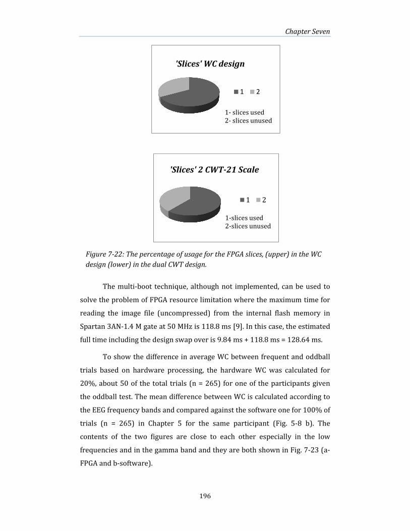
Chapter Seven
196
The multi-boot technique, although not implemented, can be used to
solve the problem of FPGA resource limitation where the maximum time for
reading the image file (uncompressed) from the internal flash memory in
Spartan 3AN-1.4 M gate at 50 MHz is 118.8 ms [9]. In this case, the estimated
full time including the design swap over is 9.84 ms + 118.8 ms = 128.64 ms.
To show the difference in average WC between frequent and oddball
trials based on hardware processing, the hardware WC was calculated for
20%, about 50 of the total trials (n = 265) for one of the participants given
the oddball test. The mean difference between WC is calculated according to
the EEG frequency bands and compared against the software one for 100% of
trials (n = 265) in Chapter 5 for the same participant (Fig. 5-8 b). The
contents of the two figures are close to each other especially in the low
frequencies and in the gamma band and they are both shown in Fig. 7-23 (a-
FPGA and b-software).
1 2
1- slices used
2- slices unused
'Slices' WC design
1 2
1-slices used
2-slices unused
'Slices' 2 CWT-21 Scale
Figure 7-22: The percentage of usage for the FPGA slices, (upper) in the WC
design (lower) in the dual CWT design.

Chapter Seven
197
7.3 FPGA Implementation of WC Based Biofeedback
As stated earlier in this thesis, biofeedback involves the participants’
observation of their electrophysiological state during a minimal delay to
permit for a monitoring and feedback response [10]. For that, real time signal
processing is essential to achieve the aimed application. This section shows
an FPGA implementation to the WC38 according to the EEG bands, which can
be possibly used for biofeedback application.
38 Typically existing measures use a single electrode site for biofeedback. However, using two
electrode sites allows a measure of the linkage (such as coherence) which taps into internal
communication or possibly information processing between cortical areas, reflecting more
1 2 3 4-0.05
-0.04
-0.03
-0.02
-0.01
0
0.01
0.02
Difference in average coherence
EEG frequency bands
frequent-oddball
Low
frequencies
(0.5-8 Hz)Alpha
(8-12 Hz)
Beta
(12-30 Hz)
Gamma
(30-53 Hz)
Figure 7-23: The mean difference between Frequent and Oddball average WC
according to the EEG frequency bands for one participant produced by (a)
FPGA-20% of trials (50 trials). (b) Software-100% of trials.
-0.05
-0.04
-0.03
-0.02
-0.01
0
0.01
0.02
Difference in average coherence
EEG frequency bands(b)
frequent-oddball
Beta
(12-30 Hz)Alpha
(8-12 Hz)
Low
Frequencies
(0.5-8 Hz)
Gamma
(30-120 Hz)
(a)
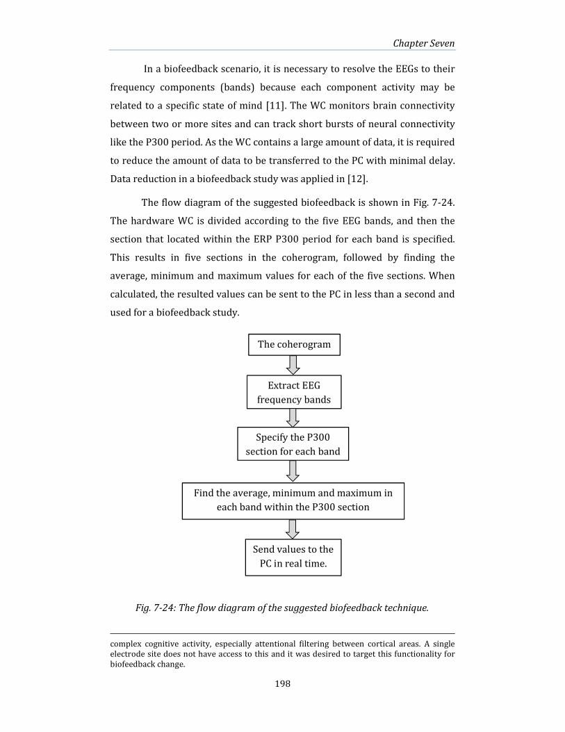
Chapter Seven
198
In a biofeedback scenario, it is necessary to resolve the EEGs to their
frequency components (bands) because each component activity may be
related to a specific state of mind [11]. The WC monitors brain connectivity
between two or more sites and can track short bursts of neural connectivity
like the P300 period. As the WC contains a large amount of data, it is required
to reduce the amount of data to be transferred to the PC with minimal delay.
Data reduction in a biofeedback study was applied in [12].
The flow diagram of the suggested biofeedback is shown in Fig. 7-24.
The hardware WC is divided according to the five EEG bands, and then the
section that located within the ERP P300 period for each band is specified.
This results in five sections in the coherogram, followed by finding the
average, minimum and maximum values for each of the five sections. When
calculated, the resulted values can be sent to the PC in less than a second and
used for a biofeedback study.
complex cognitive activity, especially attentional filtering between cortical areas. A single
electrode site does not have access to this and it was desired to target this functionality for
biofeedback change.
The coherogram
Extract EEG
frequency bands
Specify the P300
section for each band
Find the average, minimum and maximum in
each band within the P300 section
Send values to the
PC in real time.
Fig. 7-24: The flow diagram of the suggested biofeedback technique.
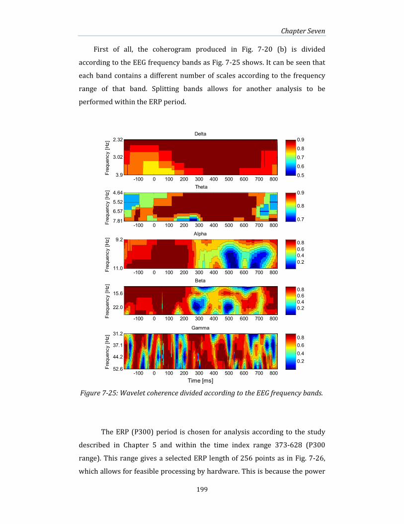
Chapter Seven
199
First of all, the coherogram produced in Fig. 7-20 (b) is divided
according to the EEG frequency bands as Fig. 7-25 shows. It can be seen that
each band contains a different number of scales according to the frequency
range of that band. Splitting bands allows for another analysis to be
performed within the ERP period.
The ERP (P300) period is chosen for analysis according to the study
described in Chapter 5 and within the time index range 373-628 (P300
range). This range gives a selected ERP length of 256 points as in Fig. 7-26,
which allows for feasible processing by hardware. This is because the power
Figure 7-25: Wavelet coherence divided according to the EEG frequency bands.
Time [ms]
Frequency [Hz]
Gamma
-100 0 100 200 300 400 500 600 700 80052.6
44.2
37.1
31.2
Frequency [Hz]
Beta
-100 0 100 200 300 400 500 600 700 800
22.0
15.6
Frequency [Hz]
Alpha
-100 0 100 200 300 400 500 600 700 80011.0
9.2
Frequency [Hz]
Theta
-100 0 100 200 300 400 500 600 700 8007.81
6.57
5.52
4.64
0.7
0.8
0.9
0.2
0.4
0.6
0.8
0.2
0.4
0.6
0.8
0.2
0.4
0.6
0.8
Frequency [Hz]
Delta
-100 0 100 200 300 400 500 600 700 8003.9
3.02
2.32
0.5
0.6
0.7
0.8
0.9

Chapter Seven
200
-200 -100 0 100 200 300 400 500 600 700 800-30
-20
-10
0
10
20
30
40
50
Time [ms]
Am
pli
tud
e [
uV
]
of two, provided in the 256 point length, facilitates the division operation and
it also covers the P300 duration. The proposed biofeedback is summarized by
calculating the average, minimum and maximum values for the WC in the
P300 period for each of the five EEG bands. The result of these calculations
can then be sent to the PC in real time and used for future biofeedback study.
The values of the FPGA based WC were stored in SRAM0 in the
address range A800-F3FF, 16-bit/value, however, only the least four bits
from each value are used to compose the WC as previously mentioned. Table
7-12 lists the WC locations in the SRAM including the ERP range where the
analysis was applied. The 256 (100hex) values in the ERP period (373-628
time index range) is the area of analysis for each EEG band as indicated
between the dashed lines in Fig. 7-26.
Figure 7-26: An EEG with the P300 component around the time index 373-628.
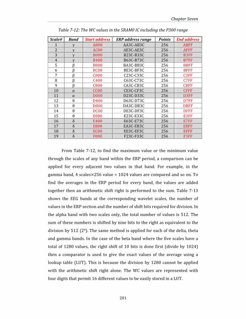
Chapter Seven
201
Table 7-12: The WC values in the SRAM0 IC including the P300 range
Scale# Band Start address ERP address range Points End address
1 γ A800 AA3C-AB3C 256 ABFF
2 γ AC00 AE3C-AE3C 256 AFFF
3 γ B000 B23C-B33C 256 B3FF
4 γ B400 B63C-B73C 256 B7FF
5 β B800 BA3C-BB3C 256 BBFF
6 β BC00 BE3C-BF3C 256 BFFF
7 β C000 C23C-C33C 256 C3FF
8 β C400 C63C-C73C 256 C7FF
9 β C800 CA3C-CB3C 256 CBFF
10 α CC00 CE3C-CF3C 256 CFFF
11 α D000 D23C-D33C 256 D3FF
12 θ D400 D63C-D73C 256 D7FF
13 θ D800 DA3C-DB3C 256 DBFF
14 θ DC00 DE3C-DF3C 256 DFFF
15 θ E000 E23C-E33C 256 E3FF
16 δ E400 E63C-E73C 256 E7FF
17 δ E800 EA3C-EB3C 256 EBFF
18 δ EC00 EE3C-EF3C 256 EFFF
19 δ F000 F23C-F33C 256 F3FF
From Table 7-12, to find the maximum value or the minimum value
through the scales of any band within the ERP period, a comparison can be
applied for every adjacent two values in that band. For example, in the
gamma band, 4 scales×256 value = 1024 values are compared and so on. To
find the averages in the ERP period for every band, the values are added
together then an arithmetic shift right is performed to the sum. Table 7-13
shows the EEG bands at the corresponding wavelet scales, the number of
values in the ERP section and the number of shift bits required for division. In
the alpha band with two scales only, the total number of values is 512. The
sum of these numbers is shifted by nine bits to the right as equivalent to the
division by 512 (29). The same method is applied for each of the delta, theta
and gamma bands. In the case of the beta band where the five scales have a
total of 1280 values, the right shift of 10 bits is done first (divide by 1024)
then a comparator is used to give the exact values of the average using a
lookup table (LUT). This is because the division by 1280 cannot be applied
with the arithmetic shift right alone. The WC values are represented with
four digits that permit 16 different values to be easily stored in a LUT.

Chapter Seven
202
Table 7-13: The EEG bands, the corresponding wavelet scales and the bit shift
required for division.
EEG bands # scales #values Shift bits Comparator
Delta 4 1024 10 -
Theta 4 1024 10 -
Alpha 2 256 9 -
Beta 5 1280 10 Yes
Gamma 4 1024 10 -
The biofeedback analysis added a few extra resources to the WC
analysis report where the number of total slices is increased from 67%
(Table 7-11) to 70% and the number of 4-input LUT from 62% to 65%. The
result of these operations on the ERP period is shown in Table 7-14. This
gives the average, maximum and minimum39 WC values between Fz-Cz for
the WC in Fig. 7-20 calculated by both FPGA and software.
Table 7-14: The average, maximum and minimum WC values in the ERP period
Table 7-14 shows high similarity between hardware (FPGA) and
software processing to the coherogram for the average, maximum and
minimum values in the ERP period for each EEG band. The total time to
calculate these values in FPGA was 0.12 ms starting from the WC values in
the SRAM or 9.84 ms (CWT and WC) + 118.8 ms (design swap) + 0.12 ms=
128.76 ms starting from the raw EEGs. These values were sent to the PC via
serial communication40 and visualized using Matlab in an average time of
39 The minimum of alpha, beta and gamma are zero due to the existence of the blue colour in
the ERP period (index 373-628), which reflects zero. See Fig. 7-25. 40 The transfer rate was 128000 bit/second.
Average WC in the
ERP period
Maximum WC in the
ERP period
Minimum WC in the
ERP period
EEG bands software FPGA software FPGA software FPGA
Delta 0.9340 0.9375 0.9375 0.9375 0.8750 0.8750
Theta 0.8817 0.875 0.9375 0.9375 0.6875 0.4375
Alpha 0.3937 0.375 0.8125 0.8125 0 0
Beta 0.5449 0.5 0.8750 0.8750 0 0
Gamma 0.7090 0.6875 0.9375 0.9375 0 0
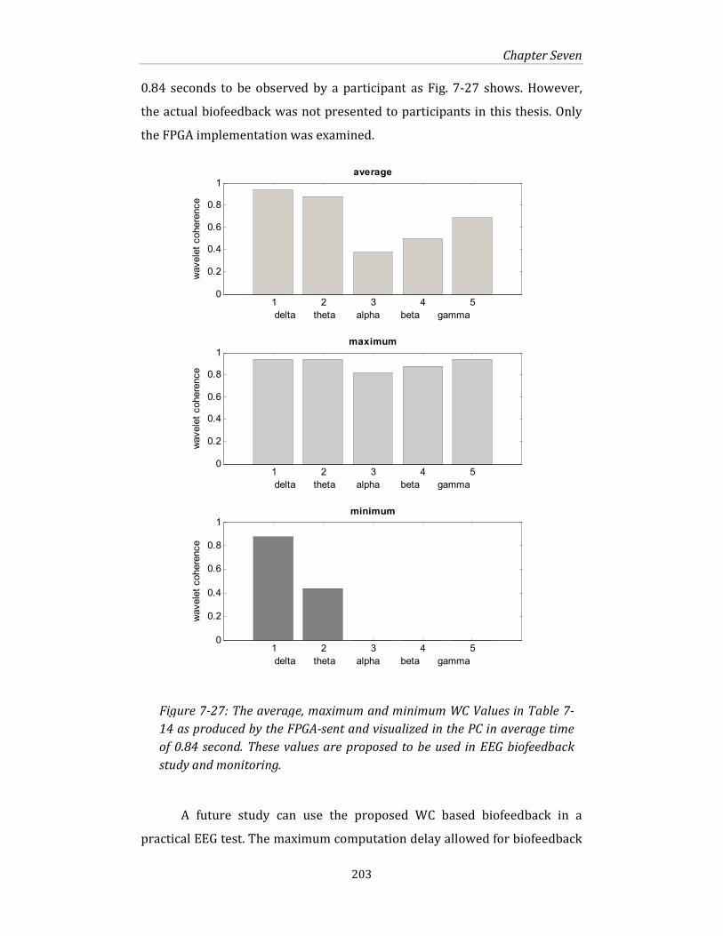
Chapter Seven
203
1 2 3 4 50
0.2
0.4
0.6
0.8
1average
delta theta alpha beta gamma
wavelet coherence
1 2 3 4 50
0.2
0.4
0.6
0.8
1maximum
delta theta alpha beta gamma
wavelet coherence
1 2 3 4 50
0.2
0.4
0.6
0.8
1minimum
delta theta alpha beta gamma
wavelet coherence
0.84 seconds to be observed by a participant as Fig. 7-27 shows. However,
the actual biofeedback was not presented to participants in this thesis. Only
the FPGA implementation was examined.
A future study can use the proposed WC based biofeedback in a
practical EEG test. The maximum computation delay allowed for biofeedback
Figure 7-27: The average, maximum and minimum WC Values in Table 7-
14 as produced by the FPGA-sent and visualized in the PC in average time
of 0.84 second. These values are proposed to be used in EEG biofeedback
study and monitoring.

Chapter Seven
204
in this context is 1 s [10]. Exceeding the maximum delay results in visualizing
the analysed EEG in a longer time frame thereby reducing the ability to act on
the applied biofeedback. The biofeedback application might be adapted for
improving cognition in patients with attention-deficit hyperactivity disorder
(ADHD) [13]. This can be achieved by measuring two EEG signals, calculating
their WC and the parameters outlined in this section for biofeedback then
visualizing these parameters to the participant in real time. The use of these
parameters in a biofeedback setting can potentially improve the user’s
attention capacity.
7.4 Summary and Discussion
This chapter has shown a novel FPGA based method to implement the
WC for a pair of EEG signals. The coefficients of two CWTs saved in the SRAM
ICs were fetched into the WC processor to calculate the wavelet coherence.
This processor was designed in VHDL and implemented on the Spartan 3AN
FPGA. The produced results show the degree of accuracy to the presented
coherogram using the moderate-specification FPGA device.
The design requires providing the basis components for the WC that
represents the WCS and the auto-spectrum of the two time series inputs.
Design requirements were researched thoroughly before the final FPGA
implementation. These were symbolized by simplifying the WC algorithm
(Fig. 7-3), finding the appropriate sample scaling factor to prevent a potential
overflow, and investigating the most suitable word length and smoothing
method.
By optimizing the WC algorithm, four operations were eliminated. The
software coherogram was computed and used as a reference to evaluate the
performance of the FPGA based one. The scalogram analysis helped in
detecting the overflow implied in the CWT through the intermediate steps
towards the WC and helped in choosing a suitable scaling factor (194) for the
samples of the EEGs and the Morlet function in hardware. In addition, it
helped in finding the best smoothing technique among several tested and
developed methods to be easily implemented in the FPGA. Image quality
methods were applied as an objective measure to select the best of these
Chapter Seven
205
developed schemes for smoothing. Furthermore, the scalogram analysis was
useful in selecting the most appropriate word length for the WC. The word
length of the 32-bit sample was a suitable option for the indices of speed-
resources in the design. The number of graded colours (16) was sufficient for
the details of the coherogram to appear. Timing simulation was performed to
verify the tasks of the design prior to the final implementation and to
compute the total clocks required for the WC in hardware.
The accuracy of the FPGA based WC plots was shown as compared
against that produced by the reference software plots using three image
quality methods. This was repeated for 10 Fz-Cz pairs of EEG trials. The
result of this comparison was represented by the indices of the image quality
where the mean of these trials was 0.0053, 0.0543 and 0.9247 for the NMSE,
NAD and the SC respectively. The mean values have indicated the accuracy
obtained by the FPGA design. The standard deviation (SD) was also
calculated and its small value showed the closeness of the image quality
measures for 10 WC trials to their mean (Table 7-10).
The FPGA was able to compute the WC in a total time of 8.7 ms at an
operational frequency of 40 MHz. Despite the fact that the CWT and the WC
designs were restricted to be merged in one large design, due to resource
limitations, the sequential implementation of these two designs was shown
to be a complete success from the produced results. Such implementation
was applicable due to the fact that the CWT results were kept in the SRAMs
during the swapping between the two implementations without loss of
information.
Finally, a system that can potentially be used for biofeedback was
presented which was based on the WC results. This was based on finding the
average, maximum and minimum values for the WC in the ERP-P300 period
and for each EEG frequency band within the FPGA. With a small amount of
data, it was possible to compute these values in 128.76 ms, send and display
them in the PC in an average time of 840 ms which is excellent for
biofeedback. Such biofeedback may be used to treat patients who suffer from
a deficit in their attention abilities.

Chapter Seven
206
7.5 References
1 A. Klein, T. Sauer, A. Jedynak and W. Skrandies, "Conventional and wavelet
coherence applied to sensory-evoked electrical brain activity,"
Biomedical Engineering, IEEE Transactions on, vol. 53, pp. 266-272, 2006.
2 V. Sakkalis, T. Oikonomou, E. Pachou, I. Tollis, S. Micheloyannis, and M.
Zervakis, "Time-significant wavelet coherence for the evaluation of
schizophrenic brain activity using a graph theory approach," in
Engineering in Medicine and Biology Society, 2006. EMBS'06. 28th Annual
International Conference of the IEEE, 2006, pp. 4265-4268.
3 L. J. Myers and C. D. MacKinnon, "The time course of functional coupling
between human cortical motor areas during internally driven vs.
externally cued movements," in Engineering in Medicine and Biology
Society, 2004. IEMBS '04. 26th Annual International Conference of the IEEE,
2004, pp. 4669-4672.
4 S. A. Markazi, S. A. Qazi, and L. K. Stergioulas, "Study of Change Blindness
EEG Synchronisation using Wavelet Coherence Analysis," in Engineering
in Medicine and Biology Society, 2005. IEEE-EMBS 2005. 27th Annual
International Conference of the, 2005, pp. 5995-5998.
5 A. Grinsted, J. C. Moore, and S. Jevrejeva, "Application of the cross wavelet
transform and wavelet coherence to geophysical time series," Nonlinear
processes in Geophysics, pp. 561-566, 2004.
6 R. Andraka, "A survey of CORDIC algorithms for FPGA based computers,"
in Proceedings of the 1998 ACM/SIGDA sixth international symposium on field
programmable gate arrays, 1998, pp. 191-200.
7 J.-P. Lachaux, A. Lutz, D. Rudrauf, D. Cosmelli, M. L. V. Quyen, J. Martinerie,
and F. Varela, "Estimating the time-course of coherence between single-
trial brain signals: an introduction to wavelet coherence," Neurophysiol
Clin, vol. 32, pp. 157-174, 2002.
8 C. Torrence and G. P. Compo, "A Practical Guide to Wavelet Analysis," Bulletin of the American Meteorological Society vol. 79, pp. 61-78, 1998.
9 Xilinx UG333 “Spartan-3AN FPGA In-System Flash User Guide”, [online],
Accessed Sept. 25, 2013: www.xilinx.com/support/documentation/user_guides/ug333.pdf
10 P. L. Purdon, H. Millan, P. L. Fuller, and G. Bonmassar, "An open-source
hardware and software system for acquisition and real-time processing
of electrophysiology during high field MRI," Journal of neuroscience
methods, vol. 175, pp. 165-186, 2008.

Chapter Seven
207
11 Q. Dong, Y. Li, B. Hu, Q. Liu, X. Li, and L. Liu, "A solution on ubiquitous EEG-based biofeedback music therapy," in Pervasive Computing and
Applications (ICPCA), 2010 5th International Conference on, 2010, pp. 32-37.
12 D. Varoqui, J. Froger, J. Y. Pélissier, and B. G. Bardy, "Effect of coordination
biofeedback on (re) learning preferred postural patterns in post-stroke
patients," Motor Control, vol. 15, pp. 187-205, 2011.
13 M. Ahmadlou, H. Adeli, and A. Adeli, "Graph theoretical analysis of
organization of functional brain networks in ADHD," Clinical EEG and
neuroscience, vol. 43, pp. 5-13, 2012.

Chapter Eight
208
Chapter 8 Conclusions and Summary
The focus of this thesis was the FPGA design and implementation of a
CWT and WC for EEG signals. The thesis was divided into three phases that
relate to the wavelet application in the EEG field. In the first phase, a novel
analysis was developed with the technique of CWT and WC. The analysis
involved the application of the WC to EEG signals to derive indices that track
the emergence of the well-known ERP-P300. This analytic approach was
performed between electrode sites that relate to the cognitive processes
engaged when an oddball event occurs amidst a series of visual stimuli.
The work in this thesis has concentrated on the FPGA implementation
of the CWT and WC for EEG and ERP signals. The FPGA based WC approach
was aimed at providing a practical means for neurofeedback training in
future work. As the biofeedback studies require real time (less than one
second latency) processing of acquired signals, the FPGA device can provide
the high speed processing required for the feedback. The CWT was
implemented and compared against other implementation methods in the
literature. The methods in the literature employed general purpose
processors or high end FPGA devices to implement the CWT. However, the
CWT method presented in Chapter 6 of this thesis has shown a higher level of
performance.

Chapter Eight
209
Chapter 7 has detailed a novel WC design and implementation based
on the outcome of the CWT design. The system was able to process EEG
signals with minimal delay and provides the means for biofeedback based on
the WC.
8.1 Wavelet Coherence Analysis for EEG Waveforms
The EEG is a weak brain activity with an amplitude of less than
100 µV and a frequency range of 0.5-100 Hz. This range was divided into five
basic bands: delta (0.5-4 Hz), theta (4-8 Hz), alpha (8-13 Hz), beta (13-30 Hz)
and gamma (>30 Hz). The appearance of these rhythms is dependent on
several factors including the mental state of the participant.
A pilot study of EEG recordings acquired during a visual oddball task
was analysed using the CWT and WC, as outlined in Chapter 5 of this thesis.
The task was to hit a key when an oddball letter appears and another key for
the frequent event. As a result, the ERP-P300 appears on the ongoing EEG
and it is more likely to appear in oddball trials. This was repeated for 12
participants with 265 trials presented to each participant. The EEG was
recorded during the task. The average WC between Fz-Cz electrodes was
determined which provided evidence for the brief activation of a fronto-
central circuit. In the average WC, a significant difference between frequent
and oddball trials was found in the low frequency band (delta and theta)
Zlow-freq= 4.6292 (P = 0.00006) and in the gamma band Zgamma= 3.273 (P
=0.00106), (see Fig. 5-8 c). These standardized normal form measures were
related to the cognitive process involved in oddball monitoring.
Comparisons of 20 different pairs in the cerebral frontal-central-
parietal sections (Fig. 5-13) showed that Fz-Cz had the best WC for the visual
oddball task. This provided a justification in using this pair as a source of data
to be analysed. It could also support future analysis in the WC for EEGs or
perhaps other electrode pairs may be more suitable depending on the nature
of the cognitive task.
In the gamma band analysis, the frequent trials produced higher
average WC values, which may reflect the continued expectation of the

Chapter Eight
210
oddball or maintenance of the memory trace that matches the frequent
stimulus event. The expectancy hypothesis was supported by the post-
oddball trial position of a series of frequent trials and showed a very high
correlation between the post-oddball position and gamma coherence
amplitude during the P300 period (350-600 ms) (Fig. 5-11 c). In conclusion,
these measurements may correspond to a form of expectancy switch, which
confirms the validity of utilizing P300 in cognition. The research presented in
Chapter 5 has resulted in the publication of a journal paper.
This work was expanded to estimate the WC of EEG signals in the
FPGA for real time applications and was investigated in Chapters 6 and 7 of
this thesis.
8.2 FPGA Based CWT for EEG Analysis
The design and implementation of the CWT in Chapter 6 of this thesis
was the preliminary step to provide the basis for producing an efficient WC
algorithm in hardware. The work presented in Chapter 6 has resulted in the
publication of three papers and one abstract presented at a conference. Two
of these papers were published in conference proceedings and one journal
paper is under review.
The CWT design was highly optimized in several schemes. These
optimizations were represented by:
(1) Performing the required processing in the frequency domain and
then mapping back to the time domain. This helped in reducing the
arithmetic operations compared against the time domain arithmetic.
(2) The storage method for the points of the Morlet wavelet function
where the wavelet function in the frequency domain contains a large number
of zeros especially at higher scales. These zeros were neglected and only non-
zeros were considered for storage.
(3) The required scales for analysis. Wavelet scales out of the EEG
frequency range were removed which resulted in saving further block RAM
and reducing calculations.

Chapter Eight
211
(4) Providing the means to operate the design with a maximal clock
frequency. A technique was made to use a block RAM to store the individual
scales of wavelet coefficients before transferring them to the external SRAM.
This helped in increasing the frequency rate of the design up to 133 MHz as it
was 125 MHz. The required time to calculate the CWT for the two EEGs was
1.14 ms only.
Three controllers were built in VHDL, in addition to the imported
Xilinx FFT core, as major operational units in the design to compute the CWT
coefficients. The involved FFT core was used to perform one FFT as well as
the IFFT for 21 times (for 21 wavelet scales). These operations were doubled
on the same core when another EEG was involved to provide the
requirements of the WC. The produced FPGA based CWT scalogram shows
the features of the EEG in the wavelet domain. Three image quality methods
were used to compare the FPGA-based scalogram plot against the theoretical
software one. These are: the normalized mean square error (NMSE) that
gives the square difference between the FPGA and the software scalogram
plot; the normalized average difference (NAD) that gives the absolute value
between corresponding hardware coefficients normalized by the software
scalogram coefficients; and the measure of structural content (SC) that
returns the structural similarity between two scalogram plots. The results
showed the validity of the hardware computation for the CWT when
compared to the theoretical result from Matlab. The NMSE = 0.0013, NAD =
0.0227 and SC = 0.9989. To conclude, these measures have indicated that the
produced FPGA scalogram is of a high quality. The wavelet coherence design
in Chapter 7 was based on the computation of the two scalogram plots of
CWT in Chapter 6.
In conclusion, the success of the mentioned optimizations was shown
by reducing the usage of the FPGA resources, reducing the number of
required operations (4096 clocks for multiplications reduced to 499 clocks
when the scales out of the EEG frequency range were omitted), saving a
considerable amount of memory (90% reduction in BRAM locations for
storing the Morlet wavelet without zeros) and increasing the maximum
Chapter Eight
212
frequency of operation. In addition, saving additional resources allows for
expanding the system to analyse two EEG signals for later WC analysis where
extra block RAM and slices were needed to store the second EEG and the
expanded CWT controller.
8.3 FPGA Based Wavelet Coherence and Biofeedback for EEG
Waveforms
A novel FPGA implementation for the WC was presented in Chapter 7 of
this thesis. A comprehensive scalogram analysis was performed to facilitate
the design procedure, including the smoothing operation and the selection of
the appropriate signal word length through the stages of the design. The
required smoothing method for the WCS and auto-spectrum was designed to
be applicable for hardware implementation. As an outcome of the scalogram
analysis, the selected word length of the 32-bit sample for the WC was a
suitable option for the indices of speed performance and resource usage in
the design. The system read the CWT coefficients in the two SRAMs and
produced the corresponding WC coefficients. VHDL code was developed to
manipulate the switching between SRAM addresses as a major part of the
smoothing technique to provide the desired coefficients.
The average of 10 image quality measures for the hardware
coherogram plots compared against the reference (software) plots was NMSE
= 0.0053, NAD = 0.0543 and the SC = 0.9247. In addition, the SD for these 10
hardware plots was calculated and showed that the individual measures
were very close to their mean.
The system was able to produce the coherogram plane of 1024 ms by
19 scales in 8.7 ms; by adding the 1.14 ms from calculating the two CWTs and
118.8 ms for design turnover, a total time of 128.64 ms was enough to
compute the hardware WC.
Such rapid WC computation supports real time applications of EEGs.
The biofeedback mechanism (based on two separate designs, the CWT and
the WC design) is one of the applications in which the participant’s EEG is
analysed and the outcome is fed back to the participant with minimal delay. A
Chapter Eight
213
latency delay of one second is an acceptable time to give biofeedback in an
EEG system. The participant observes the outcome and updates his mental
activity according to that. The biofeedback mechanism was proposed and
implemented in the FPGA in section 7.3 to reflect the ERP generated by the
brain channels Fz-Cz in the means of coherence. The calculated coherogram
was divided into partitions according to the EEG frequency bands. Each
partition was then transferred to the PC online after finding the maximum,
minimum and the average WC coefficients in the P300 period for each of the
five EEG bands. Only 0.12 ms was enough to calculate the biofeedback values.
The biofeedback design can be used as a portable system to perform the
application.
In conclusion, the WC was estimated in the FPGA with the accuracy
measures listed in Table 7-10 and within 128.64 ms, which allows it to be
used in real time EEG applications. For the biofeedback, 128.76 ms was the
total computation time required starting from the raw EEGs. The work
presented in Chapter 7 has resulted in a journal article.
8.4 Future Work
As a suggested extension to the research presented in this thesis, this
section outlines possible improvements in both the data analysis and FPGA
phases. In the data analysis phase, and specifically the gamma correlation,
long runs of frequent trials (12-15) following the oddball could be examined
in an extended version of the task to extend the expectation of the oddball
event. It could then be determined whether the correlation is maintained
beyond the relatively modest six trials in the presented experiment (Fig. 5-9
a). In addition, a higher density of electrodes, such as a 128-channel system,
can be applied to test the connectivity between neighbouring electrodes
represented by gamma WC. With this number of channels, the distance
between neighbouring electrodes is shorter than that in the 32-electrode cap
and allows for finer connectivity tests between them.
Future development in the hardware design could focus on employing
an FPGA device with more advanced features than the one involved in this
Chapter Eight
214
thesis. For example, the recent Virtex FPGA devices could be used with their
embedded DSP slices, larger memory, additional multipliers and their ability
to operate on higher clock rates. In such a case, both the CWT and the WC
design can be combined into a larger design, which allows for improving the
performance of the overall system. In this case, the SRAM ICs (located on the
NanoBoard) are no longer required to swap between the CWT design and the
WC design. This is because more advanced FPGA devices can operate on
higher clock rates. They are also provided with a larger size of block RAM
which eliminates the need for the SRAM ICs that restrict the maximum
operational frequency of the design.
The involvement of higher-resourced FPGAs allows further extension
in the word length used to represent the samples of the input signals and the
internal signals through the design without concern for the available
resources. This would result in a reduction in the quantization error in the
final scalogram/coherogram plots thereby improving the objective measures
of these plots when compared against their software counterparts. In the
case of using the same FPGA applied in this thesis, and to overcome slice
limitations, the multi-boot technique can be adapted (which allows for the
dynamic reconfiguration of the FPGA).
Another development in the FPGA design is to use the FFT core in
advanced configurations and parameter options. The FFT core can be
employed with the available pipelined architecture that is able to load,
calculate FFT and unload the output at the same time. As a result, the speed
of performance would be increased. This can be achieved with a more
advanced FPGA than the one used in this thesis.
The streaming analysis of data can also be considered in the future
instead of using one second epochs. In addition, moving the design off the
development FPGA board to a dedicated FPGA in a printed circuit board
(PCB) is another future option.
The proposed biofeedback system can be applied in a future study.
The study will entail measuring a pair of brain channels during an EEG test,
Chapter Eight
215
processing the measured ERPs with the WC according to the EEG bands and
then displaying the result to the participant, e.g. gamma coherence. This
approach may be used for improving cognition in patients with attention-
deficit hyperactivity disorder (ADHD) since the patient is able to monitor his
generated brain activities in real time.
8.5 Thesis Conclusion
In conclusion, this thesis has presented a novel method to examine the
FPGA design and implementation of the CWT and WC for EEG signals. The
development of a low cost FPGA system for WC at high performance speed
has been demonstrated. The FPGA system illustrated in this thesis can
identify localized time-frequency features in the EEG and ERP waveforms to
provide the means of biofeedback tools. The system was employed for real
EEG measures and the results underscore the validity of the technique.
Overall, this thesis demonstrated the design and implementation of
FPGA based CWT and WC for EEG and ERP signals, which resulted in a
system suitable for real time applications.
Top Related