


Languages
Pages
Legal

LIMM IST-2001-35503 Light Induced Molecular Movements. Photo-gated devices
Final Report Covering the period 1/7/2002- 30/6/2005
Contract start date 1/7/2002 Duration: 36 months Project coordinator: Universiteit van Amsterdam Partners: Universiteit van Amsterdam, Université de la Mediterranée (U-II-F), Universität Bonn, Centre National de la Recherche Scientifique - Delegation Ile-de-France Ouest et Nord, Università di Ferrara, University of California, Los Angeles
Project funded by the European Community under the “Information Society Technologies” Programme

Final Report IST-2001-35503 LIMM
2
Table of contents Summary 3 Overview of the results obtained during the project 4 Summary of the deliverables and milestones accomplished 5 WP1: Synthesis of functional azobenzene derivative 7 WP2: Photophysical characterization of functional azobenzene systems 24 WP3: Light-controlled movement in confined liquid phases and sol-gel films 39 WP4: Photo-controlled vectorial motion of azo-compounds for nano-scale 53 patterning of thin polymeric films WP5: Photocontrolled current between electrodes across molecular wires 86 WP6: Light controlled single molecule motion on surface 98 WP7: Light-induced positioning and self-assembly of molecules 109 between electrodes WP8-9-10: Project management/ Self assessment/Dissemination 110

Final Report IST-2001-35503 LIMM
3
Summary of the project The aim of our project is to develop a new technology of non-contact manipulation of (individual) molecules which should permit the displacement and positioning of (individual) functional species inside a matrix or in organized monolayers. The external input we wish to use is light and it will represent the fuel that the molecules (machines) will use for their movement. In this project we intend to achieve light controlled vectorial transport for information and electronic applications. The objectives of the project are: 1. Transport of ions or molecules in organized structures This part of the project deals with the possibility to transport in solution ions or molecules in a gated system that can be opened or closed upon light excitation. Light will be used to induce a chemical (e.g. hydrophobic vs. hydrophilic) or physical change (e.g. charged vs. neutral) in a functionalized photoactive matrix, sol-gel or lamellar film that will produce a “flow” of ions or neutral molecules in a desired direction. The (highly challenging) goals of this sub-project can ultimately lead to photo-gated devices of a completely novel type. The use of this approach for micropumping in e.g. lab-on-a-chip applications may, however, be closer to realization, and can become a useful spin-off of the present proposal. 2. Light control of individual molecule motion at the nanometric scale In this objective we intend to develop a method in which by controlling optically the motion and positioning of individual molecules with a nanometric precision we can pattern a surface (or a thin film) with a spatial resolution of a few nanometers. This non-contact optical patterning technology will be based on the combination of different scaning probe techniques with near-field optics. 3. Nanosized electronic device by light controlled positioning and self-assembly of molecules between electrodes. In this last and very challenging part of the program we intend to develop photoswitchable junctions in which photoactive groups are responsible for different electrical conduction upon light excitation; light active systems able to orient and self assemble in order to form a bridge between two metallic electrodes. We will operate in three different media: 1) solution, 2) polymer and sol-gel matrices and 3) surfaces, to build up knowledge, design and develop both i) proof-of-principle devices and ii) nanostructures of few nanometers dimensions based on self organizing molecular systems. This will eventually bring us to the realisation of a photogated electronic device.
Final Report IST-2001-35503 LIMM
4
Overview of the most important results obtained during the project The LIMM has been a very successful and enjoyable project at the interface between different disciplines and with a strong collaboration between the groups and important results which are summarized in this last report. The project resulted also in exchange of people and knowledge, in the development of new techniques and machines, and in the publication of 5 papers and more than 10 in preparation and amongst them in a paper to be submitted to Science. Most of the results have been already presented in international meeting and have received a lot of attention. Finally we believe that the combination of light and mechanical movements is unique and opens important and numerous applications from electronic devices to biomedicine. The results obtained in the LIMM project can be summarized according with the objectives and aims proposed in the working plan. In particular we have been able to address and successfully complete the following points.
1. We have designed and fully investigated new class of molecules containing azobenzene functionalities able to undergo to reversible photoisomerization (Z-E forms) upon light excitation.
2. The rates, yields and the mechanism of the photoinduced reactions have been determine and the processes investigated in solution, anchored to metal surfaces and silica, and also embedded in polymeric matrices.
3. The photoresponsive systems have been immobilized inside silica nanochannels, prepared using sol-gel techniques, and their behavior studied using emission spectroscopy. We have demonstrated that the photoisomerization process is not prevented in such a matrix.
4. For the first time light induced movement of a dye entrapped in the mesoporous upon photoisomerization of the azobenzene molecules have been demonstrated using different type of spectroscopy.
5. Large scale nanopatterning of surfaces have been obtained using azo-film and an interference technique developed by the consortium during the project. The pattern can be extremely regular and the spots obtained can be of the order of less than 180 nm.
6. Photoswitchable breakjunctions have been made and it has been demonstrated that the conductivity between two electrodes dramatically changes going from the E form to the Z isomer due to a different conformation of the molecule.
7. We were not able to observe single molecule movement on a surface but a random walk method has been developed to simulate such a behavior.

Final Report IST-2001-35503 LIMM
5
Summary of the deliverables and milestones accomplished during the project All the deliverables proposed have been achieved except for D17 (in red) and part of D18. Also all the milestones have been achieved except for the last two M5, M6 which because of time restriction have not been completed. A list of all the deliverables and milestones are reported below. Del no
Deliverable name WP no
Lead participant
Estimated person month
Del. type
Secu-rity
Delivery (proj. month)
D1 Report on progress on the synthesis.
1 P3 2 R Pu 12
D2 At least 3 new azo-benzene derivatives with different functional groups.
1 P3 56 P Rest 12
D3 First Annual Report 8 P1 1 P Rest 12 D4 Progress report about the
spectroscopy of all the compounds under investigation.
2 P1 18 R Pu 18
D5 Measurements of the rate of isomerization and therefore of the switching rate of the compounds.
2 P1 10 R Rest 24
D6 Report on synthesis of dendron substituted azobenzenes
1 P3 2 R Pu 24
D7 At least 2 novel compounds containg dendron substituted azobenzenes.
3 P3 8 P Rest 24
D8 Report on the construction of photoactive sol-gel films.
3 P6 23 R Rest 24
D9 At least 2 sol-gel films containing photoactive systems.
3 P6 15 P Rest 24
D10 Report on nano-scale optical patterning of thin azo-polymer films and sol gel
4 P4 28 R Pu 24
D11 At least one nano-patterned surface
4 P4 24 P Rest 24
D12 Report of the characterization of the mixed SAMs and on the electrical measurements using the Hg-based junction
5 P5 22 R Pu 24
D13 Second Annual Report 8 P1 2 R Rest 24 D14 At least 2 nanojunctions
containing different photoactive systems.
5 P5 40 D Pu 30

Final Report IST-2001-35503 LIMM
6
D15 Report on the observation of
light induced single molecule motion
6 P2 14 R Pu 30
D16 Prototype of a combined AFM/optical microscope
6 P2 36 D Rest 35
D17 Report on the optical control of the positioning of a single molecular complex onto a surface.
6 P4 4 R Pu 35
D18 Prototype of a photogated device.
7 P2 38 D Rest 36
D19 Third annual report 8 P1 2 R Pu 36 D20 Final Report 8,9 P1 0.5 R Pu 37 D21 Power Point presentation 10 P1 0.5 R Pu 3-6 Milestones M1. Synthesis and characterization of new photoactive systems. M2. A proof-of-principle device such a nanopump that can be controlled by light M3. Photo-controlled nano-scale patterning of thin films. M4. Prototype junction to proof that SAMs formed of photoactive units can gate current. M5. Photo-controlled self assembly of molecular wires between electrodes M6. Nanosized electronic device assembled by light controlled positioning of molecules

WP1. Synthesis of functional azobenzene derivative
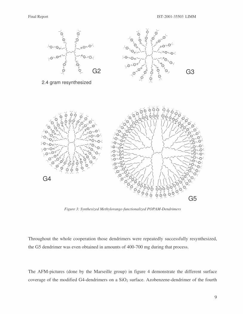
1. Azobenzene-functionalized POPAM-Dendrimers
The main aim of these syntheses is the controlled positioning and / or motion of single compound
molecules on different surfaces. This should enable the controlled formation of reversible surface-
structures with nanoscale-resolution.
For the specific AFM single-molecule experiments the periphery of the POPAM-dendrimers was
“decorated” with azobenzene. A range of POPAM-dendrimers from generation 2 up to generation
5 was synthesised in pure form, containing up to 64 azobenzene groups in the periphery of the
highest synthesized generation (fig. 1).
N N
N
N N
N
N
NHN C
N
HN C
N
NHC
N
NHC
N
NHC
N
HNC
N
HNC
N
HNC
NN
N
NN
N
N
N NH
C
N
NHC
N
HNC
N
NHC
N
HNC
N
NHC
N
NHC
N
NHC
NN
N
N
N
N
N
N
N
N
N
NN
N
N
N
O
O O
O
O
O
O
OO
O
O
O
O
O
O
O
N N
NN
N
N
N
NN
NN
N
N
N
NN
NN
N
N
N
N N
NN
N
N
N
N N
NN
HNO
NN
HNO
NN
HNON
N
HN
ONN
HN
O
NN
HN
O
NN
HN
O
NN
HN
O
NNHN
O
NN
NHO
NN
NHO
NN
NHO
NN
NHO
NN
NHO
NN
NHO
NN
NHO
NN
NHO
NN
NHO N
N
NH
ONN
NH
O
NN
NH
O
NN
NH
O
NN
NH
O
NNN
H
O
NN
NH
O
N N
HNO
N N
HNO
N N
HN O
N N
HN O
NN
HN O
NN
HN O
NN H
NO
N NH
HN
NNH
HN
N
NNH
NH
NHN
HN
N
N
C
N
O
N
C
N
O
N
C
NO
N
C
N
O
N
C
N
O
N
C
N
O
N
C
N
O
NCN
O
N N
N
NN
N
N
N
NN
N
NN
NN
NH
NN
NH
NN
NH
NN
NH
NN
NH
NN
NH
NN NN
NHNH
O
O
O
OO
OO
O
N
N
N
N NN
N
NN
NH
NN
NH
NN
NH
NN
NH
NN
NH
NN
NH NN
NN
NHNH
O O O OO
OO
O
N
N
N
N
N
N
N
NN
NH
NN
NH
NN
NH
NN
NH
NN
NH
NN
NH
NN
NN
NH
NH
O
O
O
O
O
O
O
O
N
N
N
N
N
N
N
N NHN
N NHN
NNH
N
NN
HN
NN
NH
NN
NH
N N
N N
HN
HN
O
O
O
O
O
O
O
O
N
N
N N
N
NN
N N
HN
N N
HN
N N
HN
N N
HN
N N
HN
N N
HN
N NN N
HNHN
O
O
O
OO
OO
O
N
N
N
NN
N
N
NN
HN
NN
HN
NN
HN
NN
HN
NN
HN
NN
HNNN
NN
HNHN
OOOOOO
OO
N
N
N
N
N
N
N
NN
HN
NN
HN
NN
HN
NN
HN
NN
HN
NN
HN
NN
NN
HN
HN
O
O
O
O
O
O
O
O
N
N
N
N
N
N
N
NN
NH
NNNH
NN
NH
NN N
H
NN
NH
NN
HN
NN
NN
NH
NH
O
O
O
O
O
O
O
O
G3
G5
G4
G2 N N
N
N N
N
N
NHN C
N
HN C
N
NHC
N
NHC
N
NHC
N
HNC
N
HNC
N
HNC
NN
N
NN
N
N
N NH
C
N
NHC
N
HNC
N
NHC
N
HNC
N
NHC
N
NHC
N
NHC
NN
N
N
N
N
N
N
N
N
N
NN
N
N
N
O
O O
O
O
O
O
OO
O
O
O
O
O
O
O
N N
NN
N
N
N
NN
NN
N
N
N
NN
NN
N
N
N
N N
NN
N
N
N
N N
NN
HNO
NN
HNO
NN
HNON
N
HN
ONN
HN
O
NN
HN
O
NN
HN
O
NN
HN
O
NNHN
O
NN
NHO
NN
NHO
NN
NHO
NN
NHO
NN
NHO
NN
NHO
NN
NHO
NN
NHO
NN
NHO N
N
NH
ONN
NH
O
NN
NH
O
NN
NH
O
NN
NH
O
NNN
H
O
NN
NH
O
N N
HNO
N N
HNO
N N
HN O
N N
HN O
NN
HN O
NN
HN O
NN H
NO
N NH
HN
NNH
HN
N
NNH
NH
NHN
HN
N
N
C
N
O
N
C
N
O
N
C
NO
N
C
N
O
N
C
N
O
N
C
N
O
N
C
N
O
NCN
O
N N
N
NN
N
N
N
NN
N
NN
NN
NH
NN
NH
NN
NH
NN
NH
NN
NH
NN
NH
NN NN
NHNH
O
O
O
OO
OO
O
N
N
N
N NN
N
NN
NH
NN
NH
NN
NH
NN
NH
NN
NH
NN
NH NN
NN
NHNH
O O O OO
OO
O
N
N
N
N
N
N
N
NN
NH
NN
NH
NN
NH
NN
NH
NN
NH
NN
NH
NN
NN
NH
NH
O
O
O
O
O
O
O
O
N
N
N
N
N
N
N
N NHN
N NHN
NNH
N
NN
HN
NN
NH
NN
NH
N N
N N
HN
HN
O
O
O
O
O
O
O
O
N
N
N N
N
NN
N N
HN
N N
HN
N N
HN
N N
HN
N N
HN
N N
HN
N NN N
HNHN
O
O
O
OO
OO
O
N
N
N
NN
N
N
NN
HN
NN
HN
NN
HN
NN
HN
NN
HN
NN
HNNN
NN
HNHN
OOOOOO
OO
N
N
N
N
N
N
N
NN
HN
NN
HN
NN
HN
NN
HN
NN
HN
NN
HN
NN
NN
HN
HN
O
O
O
O
O
O
O
O
N
N
N
N
N
N
N
NN
NH
NNNH
NN
NH
NN N
H
NN
NH
NN
HN
NN
NN
NH
NH
O
O
O
O
O
O
O
O
G3
G5
G4
G2
Figure 1: Azobenzene-functionalized POPAM-dendrimers

Final Report IST-2001-35503 LIMM
8
Figure 2 shows the subsequent steps of the POPAM-dendrimer synthesis here considering the
fourth generation (G4) dendrimer as an example.
NN
O
Cl
NEt3, CHCl3/CH2Cl2
CNH
NN
O
NH2
8,16,32,648,16,32,64
NN S
N O
OCl
CNH
NN
O
32
=
oder
NN
NN
N
N
N
NN
NN
N
N
N
NN
NN
N
N
N
NN
NN
N
N
N
N N
NN
HNO
NN
HN
ONN
HN
ONN
HN
O
NN
HN
O
NN
HN
O
NN
HN
O
NN
HN
O
NN
HN
O
NN
NHO
NN
NHO
NN
NHO
NN
NHO
NN
NHO
NN
NHO
NN
NHO
NN
NHO
NN
NH
O NN
NH
ONN
NH
O
NN
NH
O
NN
NH
O
NN
NH
O
NNN
H
O
NN
NH
O
N N
HNO
N N
HNO
N N
HN O
N N
HN O
NN
HN O
NN
HN O
NN H
N
O
G4
3-7 d, RT
Figure 2: Synthesis of the G4 POPAM-Dendrimer decorated by 32 azobenzene units
2. Methylorange-functionalized POPAM-Dendrimers
In order to obtain further suitable molecules for the AFM-measurements the POPAM-dendrimers
were also functionalized with methylorange-units, in the range of G2 to G5.
The G2-dendrimer was obtained on a gram-scale and could be used for the preparation of
photoactive films.
All of the POPAM-dendrimers synthesized by the Bonn group were photophysically characterized
by the group of De Cola et al.
or
Final Report IST-2001-35503 LIMM
9
NN
N
NN
N
N
NHN
OS
O
N
NH
OSO
N
NH OSO
HNOS
O
N
NH
OS O
N
HN
OS
O
N
HN
OSO
N
HN
OSO
NN
N
NN
N
N
N NHO
SO
NHNO
SO
N
HNOS
O
N
NHO SO
N
HN
O SO
N
NH
OS
O
N
NH
OS O
N
NH
OS O
NN
N
N
N
N
N
N
N
N
N
NN
N
N
N
N
N
N
N
N
N
N
N
N
N
N
N
NN
N
N
N
NN
NN
N
N
N
NHN
OS
O
N
NH
OS
O
N
HN
OS
O
N
NH
OS
O
N
HN
OSO
N
NH
OSO
N
OSO
HNNH
OSO
NN
NN
N
N
N
N NHO
SO
N
HN
OS
O
N
NH
O
SO
N
NH
OS
O
N
NH
OS O
N
HN
OS O
N
OS O
NH
N
HN
OS O
NN
NN
N
N
N
N
HN
OSO
N HN
OS
O
N
NH
OSO
N
HNOS
O
N
HNO S
O
N
NHO S
O
N
HNO SO
N
HN
O SO
NN
NN
N
N
N
NH
OS O
N
NH
OS
O
N
HN
OSO
N
NH OSO
N
NH OSO
N
HNOS
O
N
NHOS
O
N
HN
OSO
N N
NN N N
N
N
N
N
N
N
N
N
N
N
N
N
N
N
NN N
NN
N
N
N
N
N
N
N
N
N
N
N
N N N
N
N
N
N
N
N
N
N
N
N
N
N
N
N
N
N
N
N
N
N
N
N
N
N
NNN
N
N
N N
N
NN
N
N
N
NN
N
N
N
NN
SNH
NN
S NH
NN
S NH
NN
S NH
NN
S NH
NN
S N
H
NN
S
NN
S
NHNH
O
O
O
O
O
OO
O
N
N
N
NN
N
N
NN
S
NH
NN
S
NH
NN
SNH
NN
S
NH
NN
SNH
NN
SNH N
N
S
NN
SNH
NH
O O O OO
O
O
O
N
N
N
N
N
N
N
NN
S
NH
N
N
S
NH
NN
S
NH
NN
S
NH
N
N
S
NH
N
N
S
NH
NN
S
NN
S
NH
NH
O
O
O
O
O
O
O
O
N
N
N
N
N
N
N
NN
S
H
N
NN
S
H
N
NN
S
H
N
NN
S
H
N
NNS
H
N
NN
S
H
N
N N
S
N N
S
H
N
H
N
O
O
O
O
O
O
O
O
N
N
N N
N
N
N
N N
SHN
N N
SHN
N N
SHN
N N
SHN
N N
SHN
N N
S
H
N
N N
S
NN
S
HNHN
O
O
O
O
O
OO
O
N
N
N
NNN
N
NN
S
HN
NN
SHN
NN
S
HN
NN
S
HN
NN
SHN
NN
SHN
NN
S
NN
S HN
HN
OOO
OO
O
O
O
N
N
N
N
N
N
N
N
N
S
HN
N
N
S
HN
NN
S
HN
N
N
S
HN
NN
S
HN
N
N
S
HN
NN
S
NN
S
HN
HN
O
O
O
O
O
O
O
O
N
N
N
N
N
N
N
NN
SN
H
NN
SN
H
NN
SN
H
NN
SHN
NN S
HN
NN S
HN
NN
S
NN
S
N
H
N
H
O
O
O
O
O
O
O
O
O
O
O
O
O O O
OO
O
O
O
OO
O
O
O
O
O
O
O
O
O
O
O
O
O
O
O
O
O
O
O
O
O
O
O
O
O
O
OO O O O O
O
O
O
O
O
O
O
O
O
O
O
O
O
O
O
O
O
O
N
N
N
N
N
N
N
N
N
N
N
N
NN
N N NN N
N
N
N
N
N
N
N
N
N
N
N
N
N
N
N
N
N
N
N
N
N
N
N
N
N
NN
NNNNN
N
N
N
N
N
N
N
N
N
N
N
N
N
G2 G3
G4
G5
24 gram re-synthesized
N
NHN
OS
O
N
NH
OSO
NN H
NO
SO
N
NHO SO
N
N
N
HN
OS
O
N
NH
OS O
N
NH
N
NH
OSO
N
NHOS
O
N
N
N
N
NN
N
N
N
N
N
N N
N
N
N
Figure 3: Synthesized Methylorange-functionalized POPAM-Dendrimers
Throughout the whole cooperation those dendrimers were repeatedly successfully resynthesized,
the G5 dendrimer was even obtained in amounts of 400-700 mg during that process.
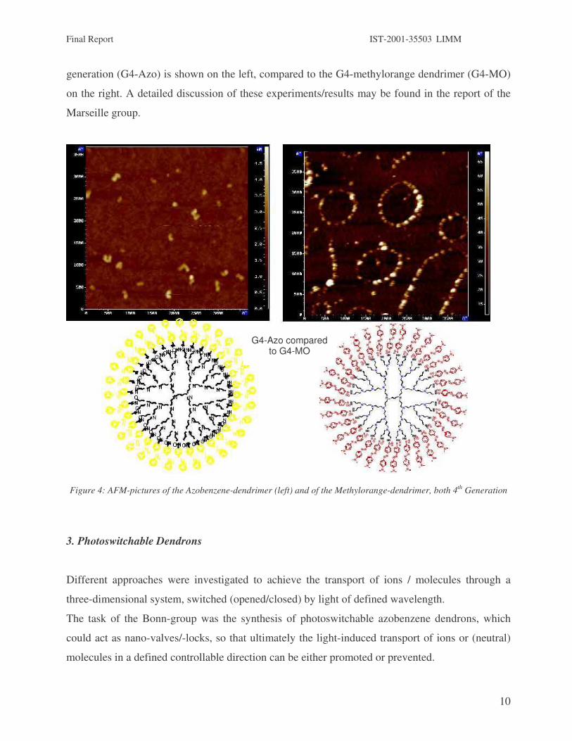
The AFM-pictures (done by the Marseille group) in figure 4 demonstrate the different surface
coverage of the modified G4-dendrimers on a SiO2 surface. Azobenzene-dendrimer of the fourth
2.4 gram resynthesized
Final Report IST-2001-35503 LIMM
10
generation (G4-Azo) is shown on the left, compared to the G4-methylorange dendrimer (G4-MO)
on the right. A detailed discussion of these experiments/results may be found in the report of the
Marseille group.
Figure 4: AFM-pictures of the Azobenzene-dendrimer (left) and of the Methylorange-dendrimer, both 4th Generation
3. Photoswitchable Dendrons
Different approaches were investigated to achieve the transport of ions / molecules through a
three-dimensional system, switched (opened/closed) by light of defined wavelength.
The task of the Bonn-group was the synthesis of photoswitchable azobenzene dendrons, which
could act as nano-valves/-locks, so that ultimately the light-induced transport of ions or (neutral)
molecules in a defined controllable direction can be either promoted or prevented.
G4-Azo compared to G4-MO
Final Report IST-2001-35503 LIMM
11
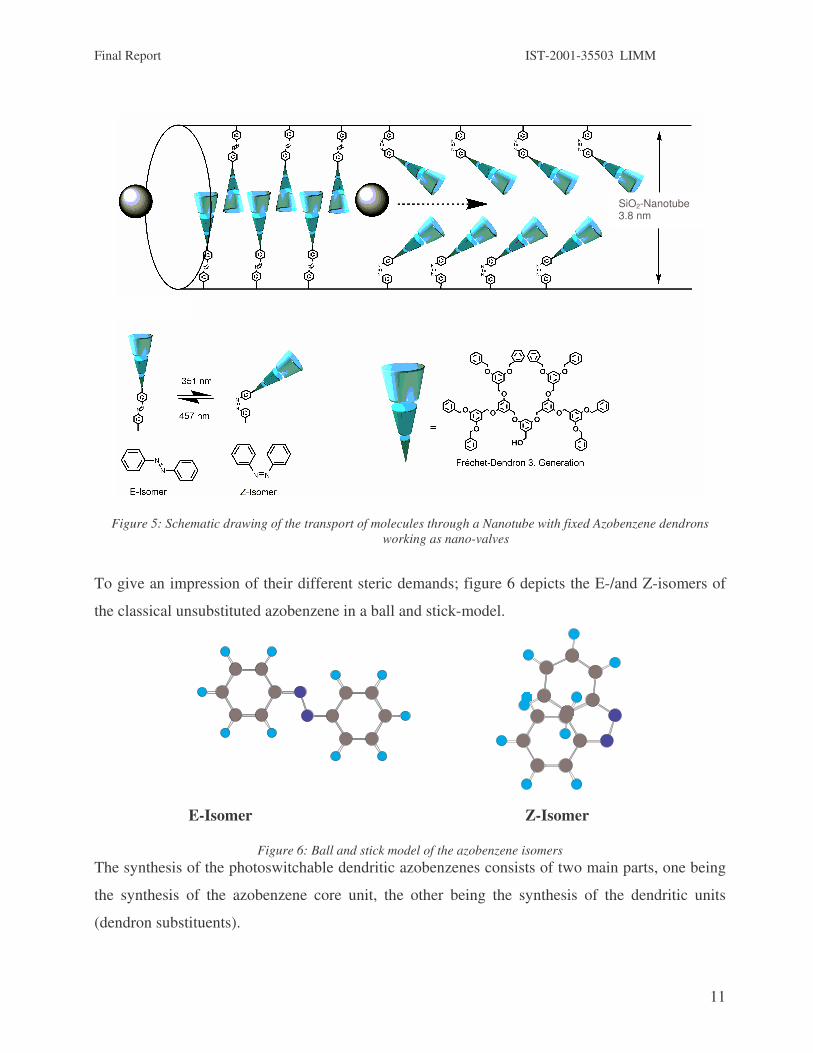
Figure 5: Schematic drawing of the transport of molecules through a Nanotube with fixed Azobenzene dendrons working as nano-valves
To give an impression of their different steric demands; figure 6 depicts the E-/and Z-isomers of
the classical unsubstituted azobenzene in a ball and stick-model.
E-Isomer Z-Isomer
Figure 6: Ball and stick model of the azobenzene isomers The synthesis of the photoswitchable dendritic azobenzenes consists of two main parts, one being
the synthesis of the azobenzene core unit, the other being the synthesis of the dendritic units
(dendron substituents).
SiO2-Nanotube 3.8 nm

Final Report IST-2001-35503 LIMM
12
The azobenzene core was obtained via classical diazotation: 4-Amionobenzylalcohol and sodium
nitrite are dissolved in ethanol/water under subsequent dropwise addition of hydrochloric acid.
This stirred mixture is added to a solution of phenol in sodiumhydroxide/water. After adjusting the
pH to 7-8 via addition of sodiumhydrogencarbonate, the product is obtained as a red precipitate,
which is recrystallized from methanol/water.
4-Aminobenzylalcohol was used as a precursor, because an elongated hydroxylic moiety inside
the molecule is needed to act as an anchor for the dendritic azobenzene inside the nanotube.
NH2 NaNO2 OH NN OH
1)H2O/Ethanol, HCl
2) H2O, NaOH
76%HO HO
Figure 7: Synthesis of the azobenzene core unit The dendritic subunits are obtained via a repetitive convergent synthesis, a method introduced by
Fréchet et al. The dendritic scaffold is built up step by step starting from the outside and
proceeding inwards.
The benzylic alcohol of the first generation is obtained after reaction of benzylbromide with
dihydroxybenzylalcohol adding potassiumcarbonate as base and [18]crown-6 as phase transfer
catalyst.
The subsequent bromination can be achieved via two synthetic routes. Route 1 involves the use of
phosphoroustribromide as the bromination reagent, which allows a smooth effective isolation of
the desired product. Route 2 which uses tetrabromomethane and triphenylphosphine as the
bromation agents, is a milder route because no free acid is generated during the reaction.

Final Report IST-2001-35503 LIMM
13
Figure 8: Convergent Synthesis of the Fréchet Dendrons of various generations
Depending on which specific dendrimer generation is attached to the azobenzene core unit, this
yields a “toolbox” of “prefabricated” building blocks for the cascade type synthesis of
photoswitchable azobenzenes.
In total six different dendritic azobenzenes were thus synthesized. The compounds were delivered
to the Zink group in Los Angeles for the insertion in the above already mentioned nanotubes, and
as well to the group of Luisa De Cola in Amsterdam (now Münster).
During the three years of our project the cooperation partners were supplied with a number of
different resynthesized azo-compounds in amounts (fig. 9) of 100-150mg for each compound.
Route 1
Route 2 Toluene
K2CO3, [18]crown6
Acetone

Final Report IST-2001-35503 LIMM
14
OO
O
OO
O
NN
HO
O
O
O
OO OO
O
O
NN
HO
O
OO
NN
HO
O
OO
O
OO
O
NN
HO
O
NN
HO
OH
NN
HO
OCH3
Figure 9: Synthesized Benzene-terminated Fréchet-Dendrons
In order to simulate different steric effects inside the nanotubes a number of naphthyl decorated
azobenzenes were synthesized. With the increase in generation the steric crowding of the
peripheral groups, because of the increasing number of naphthyl groups is growing. This results in
specific differences in the photophysical behaviour of those naphthyl decorated Fréchet-dendrons
compared to the benzene-terminated Fréchet-dendrons, like light-harvesting effects caused by the
chromophoric naphthalene units.
OO
OOO
O
HO
NN
O
NN
O
O O
HOHO
NN
O
Figure 10: Naphthyl-terminated Fréchet-Dendrons with azobenzene core
The synthetic route for the naphthyl-terminated Fréchet-dendrons was chosen analogous to the
preparation of the benzene terminated Fréchet-dendrons (fig.11).

Final Report IST-2001-35503 LIMM
15
Figure 11: Synthesis of the Naphthalen-decorated Fréchet-dendrons
4. Push-pull-azobenzene Dendrons
As already mentioned the results of the AFM experiments showed a different surface coverage for
the methylorange-dendrimers compared to the azobenzene-dendrimers. In order to enable the
Marseille and Amsterdam groups to investigate possible electronic effects, the concept for a new
photoswitchable dendron was developed: The projected nitro-azobenzene compounds include just
one single photochromic unit in contrast to the above mentioned POPAM dendrimers, therefore
making it possible to detect the light induced motion of a single molecule. A further advantage of
this concept is the possibility of adapting the (nano-)size of the compounds, depending on the
generation of dendrons used.
K2CO3
[18]crown-6 Acetone
K2CO3
[18]crown-6
Acetone
Final Report IST-2001-35503 LIMM
16
OO
O
OO
O
N N
O
O
O
OO OO
O
O
NO2
OO
O
OO
O
N N
O
NO2
N N
O
NO2
N N
OH
NO2
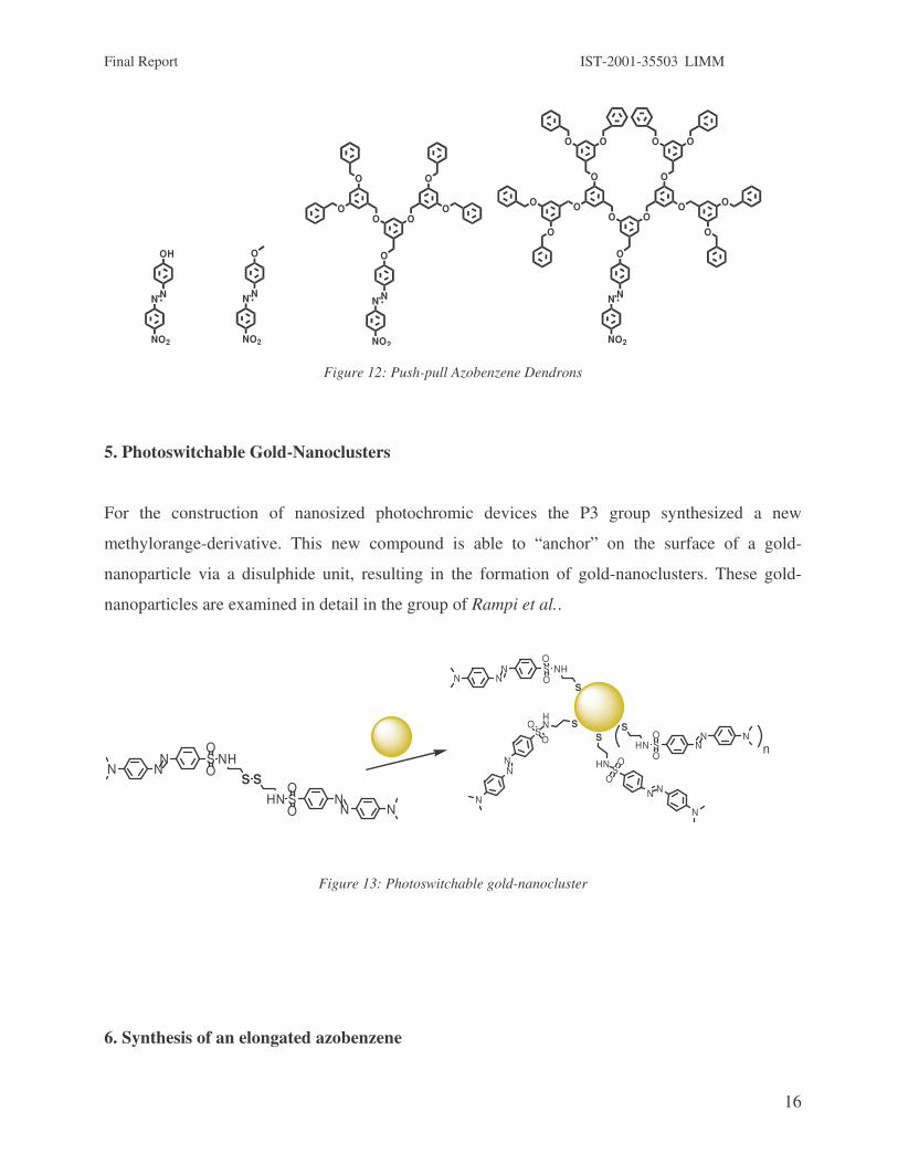
Figure 12: Push-pull Azobenzene Dendrons
5. Photoswitchable Gold-Nanoclusters
For the construction of nanosized photochromic devices the P3 group synthesized a new
methylorange-derivative. This new compound is able to “anchor” on the surface of a gold-
nanoparticle via a disulphide unit, resulting in the formation of gold-nanoclusters. These gold-
nanoparticles are examined in detail in the group of Rampi et al..
NNN S NH
O
OS
N NNSHN
O
O
S
NNN S NH
O
OS
N NNSHN
O
OS
N
N
N
S
HNO
O
S
N
N
N
SHN
O
O
Sn
Figure 13: Photoswitchable gold-nanocluster
6. Synthesis of an elongated azobenzene

Final Report IST-2001-35503 LIMM
17
For investigations described in WP5 concerning the light-driven positioning and self-organisation
between two electrodes the synthesis of a more spacering azobenzene analogous biphenyl
compound was necessary, which also included a thiol-functionality for attachment to the gold
surface. In order to obtain the desired compound, 4-tolyl-boronic acid and 1-bromo-4-
nitrobenzene were reacted under Suzuki-conditions, affording long colourless needles of the 4-
nitro-4’methylbiphenyl-compound in 70% yield.
THF, r.t., 2d
B(OH)2 Br+ Pd(PPh3)4 NO2
NN
NN
NN
Br
BrBr
LiAlH4
NO2
NBS
NN
NN
HS
HSSH
C
S
NH2H2N
Figure 14: First synthesis plan for elongated and bi-functionalised azobenzene (crossed out arrow mark non-successful steps)

Final Report IST-2001-35503 LIMM
18
Further treatment with lithiumaluminiumhydride in THF-solution, followed by stirring the
reaction mixture at room temperature for 48 hours, yielded the orange-gold coloured 4,4’-
dimethylazobiphenyl-compound.
The subsequent NBS-bromation though was not successful as indicated in the illustration above.
Table 1 informs about the synthetic attempts with their specific reaction conditions, times,
solvents stöchiometric amounts etc..
NBS Equivalent Solvent Reaction time (under reflux, two 500 W lamps
NBS-Addition
1 2 5 10
Tetrachlorkohlenstoff Chloroform Benzen Ameisensäureethylester
48 h All at once portions
Table 1: Different reaction conditions for the attempted NBS-bromination (fig. 14)
To conquer the synthetic difficulties, Prof. Vögtle suggested to introduce M. Mayor’s group to the
LIMM-team. Using its specific expertise, the Mayor group (Karlsruhe) developed a different
synthetic strategy, based upon the experiences of the Bonn group, the new strategy made use of an
aromatic thiol-function, which avoided the NBS-bromation in the benzylic position, and on the
other hand, included a different coupling method taking into account the obtained low yields of
the LiAlH4-reduction (fig.14).
7. Dye–functionalization studies
To study the motion of a single molecule in detail, we tried to label an azobenzene-unit with a
fluorescent dye. One of the required properties of a suitable dye compound is an absorption
maximum at a wavelength of approximate 550 nm. For preliminary experiments Roche Company
(Penzberg) kindly supplied 40 mg of an Oxazine-dye.

Final Report IST-2001-35503 LIMM
19
N O
N
O
HO
N
ClO4
Roche-Dye
Figure 15: Roche-Dye
We already successfully synthesized a new methylorange-derivative (fig. 16) with a silica-tripod-
anchor to enable the coupling reaction with the Roche-oxazine-dye.
Figure 16: Functionalized Methylorange compound of tripod type
The following activation of the Roche-dye (activated ester) and its reaction at the sulphonamide-
nitrogen of the new methylorange building block under C-N bond formation was not successful.
On the one side due to the high prize of the Roche-dye (100 mg cost 4500 €) we did not have
enough amount of the dye in order to gain further experiences, on the other side caused by the salt
character of the dye and its very low solubility in organic solvents this would have been necessary.
NN N
S
O
O
Cl
2 H5C2H5O
C2H5O 60%
+ NH2
Si
C2 H5 OC2 H5 O
C2 H5 OBenzene
DMPA, 3h,
r.t.
NN N
S
O
O
HN
Si
OC

Final Report IST-2001-35503 LIMM
20
Figure 17 shows a photo of a preparative TLC of the above mentioned reaction after heating for
days in pyridine. In the middle the reaction mixture is shown, on the left the spots of the pure
Roche-dye before the start of the reaction, and on the right the spots of the pure methylorange
compound before the reaction starts. (The TLC indicates in addition, that the dye delivered by
Roche was composed of several components, which certainly is a disadvantage for following
reactions.)
Figure 17: Preparative TLC of the reaction product (middle) with Methylorange precursor (right) and the Roche Dye itself (left side)
Alternative dyes were therefore chosen with similar properties regarding the absorption: Oxazin
170, Cresyl Violet, and Nile blue (fig. 18). These were reacted with the sulfonic acid chloride of
Methylorange (fig. 16, left upper formula) in order to close the SO2N-dye bond. Pyridine was used

Final Report IST-2001-35503 LIMM
21
for base and solvent here as well. Yet the solubility properties were similar unfavourable as the
Roche-dye.
O
N
NH
NH
ClO4
O
N
H2N NH2
CH3COO
O
N
H2N N
ClO4
Oxazin 170
Cresyl Violet
Nile Blue
O
N
H2N N
ClO4
Figure 18: Different oxazine dyes
Another reason for the reaction difficulties is that the direct functionalization is hampered by the
mesomerism effect of this cyanine type of dyes which decreases the nucleophilicity of the nitrogen
and consequently the possibility for a nucleophilic reaction with our new methylorange compound
(fig.16). Yet even if pyridine was used as solvent and base it failed. Even by use of different
spacers, e.g. elongated diamines, the reaction was not successful.
The supramolecular strategy to substitute the dye counter ion of Nile blue (perchlorate) directly by
a methylorange-anion (shown in fig. 19) failed, too.
Both ions, the positively charged dye and the negatively charged azobenzene should form a strong
salt bridge. The advantage of this chosen strategy would have been the possibility, that any
positive charged dye could be used in future.
no relevant reaction
“Electrophilic“ Amino-Group
through Cyanine-configuration
85% no relevant reaction (starting material) 15% brown “product” not soluble chromatography and analytics difficult

Final Report IST-2001-35503 LIMM
22
O
N
H2N N
ClO4
O
N
H2N N
ClO4
N
NN
SO
OO
O
N
H2N N O
N
H2N N
N
N N
SO
OO
Anion exchange by Methylorange sodium salt
- NaClO4
Figure 19: Ion exchange and (supramolecular) salt formation between Nile blue and Methylorange
8. Photoswitchable Cyclam derivative
Figure 20: Photochromic Cyclam
Cyclam has successfully been functionalized by us with Fréchet-Dendrons, but the attempted
functionalization with an azobenzene-moiety in our hands was not successful. It seems that the
sulfonamide bond (fig. 20) does not form easily possibly due to hydrogen bonding or steric
hindrance. For an alternative route we tried to use bromo-functionalized azobenzenes, but this step
was not successful until now.

Final Report IST-2001-35503 LIMM
23
9. Dendritic compounds with a rigid unit
For the Zink group we synthesized new acetylene substituted azobenzenes, because the LA group
needs a new system with a rigid spacer unit for further studies e.g. fixing it inside nanotubes and
on surfaces.
3,3’-Dibromoazobenzene was converted in a typical Sonogashira coupling procedure with
trimethylsilylacetylene to 3-trimethylsilylacetylene-3’-bromo-azobenzene. At the moment the
yield is 48% and we further develop the reaction conditions (solvent, temperature and reaction
time) to optimize the yield of the red solid.
Br
N
N
Br
N
N
Br
TMS
Pd(PPh3)2Cl2 PPh3, CuI
TMS
THF / NEt380°C, 12 h
Figure 21: Preparation of 3-bromo-3’-trimethylethinyl-azobenzene
Afterwards this azobenzene is converted to 3,3’-bis(trimethylsilylacetylene)-azobenzene, again via
Sonogashira coupling. Purification of the crude product is in progress.
N
N
Br
TMS
Pd(PPh3)2Cl2 PPh3, CuI
TMS
THF / NEt380°C, 12 h
N
N
TMS
TMS
Figure 22: Synthesis of the bis-ethinyl-substituted azobenzene

Final Report IST-2001-35503 LIMM
24
In both cases, mono- and bis-ethinyl-substituted azobenzene, cleavage of the trimethylsilyl-group
can be performed with tetrabutylammoniumfluoride in dichloromethane at room temperature; the
yields are approximately quantitative.
R2
N
N
R1
R2
N
N
R1
TBAF
CH2Cl2, r.t.
R1 = Br, TMS
R2 = TMS
R1 = Br,
R2 =
H
H
Figure 23: Selective Cleavage of the trimethylsilyl-group in the presence of an azo-group.
10. Conclusion
We synthesized a carefully selected number of functional azobenzene- and methylorange-
derivatives for light controlled movement in confined liquid phases and for light controlled motion
of single molecules on surfaces. All promising compounds have been delivered in sufficient
amounts to the cooperation partners. In many cases, the preparation had to be repeated in order to
be able to offer reasonable amounts for more than one spectroscopic method or for nanotube
preparations by the collaboration partners.
Following the advice of the European evaluators we concentrated our efforts on the synthesis of
strictly selected photoswitchable dendritic compounds.

Final Report IST-2001-35503 LIMM
25
O
O
O
O
O
O
OH
OH
O
O
WP2: Photophysical characterization of functional azobenzene systems
The photophysical properties of all the compounds prepared in WP1 and relevant for the LIMM
process have been investigated in solution and on solid substrate in order to determine the yields
of the trans-cis photoisomerization and their thermal back reactions. Here we discuss some of the
relevant results for the compounds reported in scheme 1 relevant for the other WPs.
AzoOH
AzoOCH3
AzoG0
AzoG1
G1
AzoG2
AzoG3
G2
Scheme 1. Chemical structures of some the studied azo compounds and dendrons and their
abbreviation.
I. Properties of azobenzene derivatized with bulky dendrimers
OH
N N
OH
OH
N N
O
O
N N
CH3
OH
O
N N
O
O
OH
O
O
O
O
O
O
O NN
OH
O NN
OHO
O
O
O
O
O
OOO
O
O
O

Final Report IST-2001-35503 LIMM
26
The absorption spectra of azo compounds are governed by two different electronic transitions,
a strong π-π* transition and a weak n-π* transition. The side groups of the azo compounds
determine the exact position of these bands. For regular trans-azobenzenes the absorption
maximum of the π-π* transition lies around 350 nm and the weak n-π* transition lies around 450
nm. If the azobenzene compound is extended with extra phenyl groups (AzoG1, AzoG2, and
AzoG3), the phenyl absorption band becomes visible around 280 nm. Functionalization of the
azobenzene on para position with an electron-accepting group leads to a charge transfer to the azo
group. Such a charge transfer can be supported by an additional electron-donating group on the
opposite phenyl ring. This is known as push-pull substitution. The effect of the charge transfer on
the absorption spectrum is that the π-π* absorption band shifts to lower energy. The n-π*
transition is practically not influenced by the substitution and therefore becomes overlapped by the
stronger π-π* band if the bathochromic shift is large enough. This push-pull substitution does not
only have an effect on the absorption spectrum, it also influences the rate of the thermal
isomerization reaction, which becomes increasingly fast and therefore shortens the cis isomer
lifetime.
Trans-azobenzene derivatives can photo-isomerize to cis compounds when they are excited at a
wavelength where the trans to cis isomerization reaction is dominant over the cis to trans
conversion. These conversion reactions are dependent on the absorption of the two isomers at the
excitation wavelength, but also on the quantum yield of the different isomerization reactions at
that wavelength. It appears that excitation in the π-π* transition leads to an overall trans to cis
isomerization while excitation in the n-π* transition leads to an overall cis to trans conversion.
The cis isomer can also thermally isomerize to the trans isomer. If a sample in the cis form is kept
in the dark it will eventually turn back into the trans form. The isomerization reaction is given by
1
2 ,
λ
λ ∆→←trans cis
II. Examination of properties in solution
A. Rate of thermal back reaction
The rates of the thermal cis to trans back reaction and quantum yields of the compounds in
scheme 1 were studied in dichloromethane solution and are summarized in Table 1.

Final Report IST-2001-35503 LIMM
27
The thermal cis to trans isomerization can be studied in the dark. An azo compound that has
been photo-isomerized with ultraviolet irradiation into the photostationary state will then only
show the thermal cis to trans reaction. The first-order rate constants can be calculated from the
change in absorbance at a certain wavelength with time using the expression
0ln ∞∆
∞
−=−t
A Ak t
A A (2)
where ∆k is the thermal rate constant in s-1, and t is time in s. 0A , ∞A , and tA are the observed
absorbances of the solution at zero time, at the end of the reaction, and at time t respectively. An
example of such an experiment is shown in Figure 1. The inset gives the ln plot of equation 2 with
a linear fit, where the slope gives the thermal rate constant.
300 400 500 600 7000.0
0.1
0.2
0.3
0.4
0.5
0 100000 2000000.0
0.2
0.4
0.6 Experimental data Linear Fit
Time / sAb
so
rba
nc
e
Wavelength / nm
ln((
A-A
)/(A
-A))
0t
∞∞
Figure 1. Absorbance evolution of AzoG1 in the dark as a function of time after irradiation
with 344 nm light to reach the photostationary state. The inset shows a linear fit of equation (2)
using the absorption data at 350 nm.
Most of the azo derivatives behave similarly, except for the rate constant of thermal AzoOH cis
to trans isomerization. The difference in rate constant can be ascribed to a deprotonation of the
hydroxy group. This hydroxy group seems to be more vulnerable to deprotonation than the
methoxy group on the other side. If the hydroxy group is replaced by a methyl ether like in

Final Report IST-2001-35503 LIMM
28
AzoOCH3, then deprotonation is prohibited and the rate constant is similar to the thermal rate
constants of the rest of the azo compounds.
A slightly higher rate constant for thermal isomerization, i.e. a faster isomerization reaction, is
found for the small AzoG0 molecule in comparison with the larger AzoG3 molecule.
Nevertheless, the differences in rate constants for the molecules are small, even though their
dimensions are very different. This can be understood by assuming that in solution only the
smaller methoxy group of the molecule, which is identical for all four cases, is actually moving
during the isomerization reaction.
Table 1. Photophysical properties of azobenzene derivatives in CH2Cl2 solutions at
room temperature.
Compound λmax
[nm]
ε(λmax)
[M-1cm-1]
ϕt→c344
ϕc→t344 ϕt→c
450 ϕc→t450 k∆
[s-1]
AzoOH 346 25800 0.20 - - - 5.84·10-4
AzoOCH3 350 29600 0.18 0.04 0.81 0.57 5.19·10-6
AzoG0 351 26600 0.33 0.03 0.40 0.61 3.32·10-6
AzoG1 351 28700 0.31 0.05 0.36 0.64 3.05·10-6
AzoG2 350 28900 0.25 0.15 0.23 0.49 3.06·10-6
AzoG3 349 41700 0.13 0.02 0.02 0.30 2.60·10-6
B. Isomerization Quantum Yields
The quantum yield for isomerization is given by:
00
1 11 10 εϕ −=
− clkI
(1)
where 0k is a zero-order rate constant for the decrease of the initial isomer concentration in
molL-1s-1, 0I is the intensity of incident irradiation light in einstein L-1s-1, ε is the extinction
coefficient at the irradiation wavelength of the solution with initial isomer in Lmol-1cm-1, c is the

Final Report IST-2001-35503 LIMM
29
concentration of this solution in molL-1, and l the path length of the light through the sample in
cm.
The extinction spectrum of the trans form is quite easily accessible. However, the extinction
spectrum of the cis isomer can also be determined if the ratio between trans and cis form, /t cr , is
known. This ratio can be obtained by comparing the 1H-NMR spectra of a non-irradiated sample
with that of an irradiated azo sample. The cis extinction spectrum is then obtained with:
/
/
11
ε ε� �� � +� �= − −� �� � � �+ � �
t cc t
t c
A c rc
l r c (3)
where A is the absorption of the irradiated sample, and /t cr is the ratio between trans and cis
isomer in the irradiated sample. Figure 2 shows the extinction spectra of both the trans and the cis
form of AzoG1 in CH2Cl2. If one compares the spectrum of the cis form with the absorption
spectrum in the photostationary state after irradiation at 344 nm, it appears that they are almost
similar. In fact it seems that in the photostationary state about 95% of the molecules is in the cis
form, while 5% of the molecules is in the trans form. For other the azo compounds these values
are similar
Once the extinction spectra of both the isomers are known, it is also possible to calculate the
quantum yields of the non-dominant isomerization reactions via the kinetic differential equation
(4), because all the other parameters can be obtained experimentally. This differential equation for
the rate processes assumes monochromatic light, complete stirring, Lambert-Beer’s law and that
the quantum yields in both directions are independent of 0I and concentrations.

Final Report IST-2001-35503 LIMM
30
300 400 500 600 7000
5000
10000
15000
20000
25000
30000
Wavelength / nm
AzoG1 trans
AzoG1 cis
Ext
inct
ion
coef
ficie
nt /
Mcm
-1-1
Figure 2. Extinction spectra of the trans and cis isomer of AzoG1.
( )'
0
1 10' ' ' ' '
'ε ϕ ε ϕ
−
→ → ∆−= − − = −
Ac t
t t c t c c t c c
dc dcI c c k c
dt A dt (4)
In this equation 0 'I , 'A , 'ε t , 'εc , 'ϕ →t c , and 'ϕ →c t are respectively the incident light intensity of
the irradiation light, the absorption of the solution at the irradiation wavelength, the molar
extinction coefficients of the trans and cis form at the irradiation wavelength, and the quantum
efficiencies of trans to cis photo-isomerization and cis to trans photo-isomerization at the
irradiation wavelength.
In such an experiment absorption spectra are taken as a function of time. The concentrations of
the different isomers can be calculated from these absorption spectra, as the extinction coefficients
of the trans and cis form of the compound are known. This gives a concentration evolution as
shown in Figure 2 for AzoOCH3. These curves can then be further analyzed by equation (4) to
result in the isomerization quantum yield data that are presented in Table 1. The results show
unusual wavelength dependence for the quantum yield of isomerization. This is a violation of
Kasha’s rule, and has been previously observed for other azobenzenes. Moreover, the
isomerization quantum yields seem to decrease with the size of the molecules, which is probably
due to a steric effect.

Final Report IST-2001-35503 LIMM
31
0 200 400 600 8000.0
1.0x10⁻⁵
2.0x10⁻⁵
3.0x10⁻⁵
4.0x10⁻⁵
Time / s
AzoG1 trans
AzoG1 cis
Con
cent
ratio
n / M
Figure 3. Concentration evolution of trans and cis Azo-OCH3. A solution brought in the
photostationary state by 344 nm light, is subsequently irradiated at 450 nm for 900 s.
Photochemical reaction on solid substrate The photochemical reaction of the above mentioned compounds covalently linked to silica and in
particular to MCM141 powder have been investigated in order to prove that the isomerization
process can occur even with bulk systems immobilized on the substrate. This knowledge strongly
contributed to the understanding of WP3 and was an essential step to assure the reversible
isomerization in the nanochannels (see WP3).
As can be observed in Figure 4 all the compounds analyzed undergo to photoreaction and the
changes observed in the absorption spectra are the same of those reported for the compounds in
solution. All the back thermal reactions have also been studied and the results summarized in
graphs and in the table reported in figure 5.

Final Report IST-2001-35503 LIMM
32
Fig. 4 Photo-isomerisation of azo derivatives in MCM-41
Fig. 5
Rate
constants for thermal isomerisation of azo derivatives in MCM-41
300 400 500 600 7000.00
0.05
0.10
0.15
0.20
0.25
Abs
orba
nce
Wavelength / nm
AzoG1-MCM41 trans AzoG1-MCM41 irradiated
300 400 500 600 7000.00
0.01
0.02
0.03
0.04
0.05
0.06
Abs
orba
nce
Wavelength / nm
AzoG0-MCM41 trans AzoG0-MCM41 irradiated
300 400 500 600 7000.00
0.01
0.02
0.03
0.04
Abs
orba
nce
Wavelength / nm
AzoG2-MCM41 trans AzoG2-MCM41 irradiated
300 400 500 600 7000.00
0.02
0.04
0.06
0.08
0.10
0.12
Abs
orba
nce
Wavelength / nm
AzoG3-MCM41 trans AzoG3-MCM41 irradiated
trans cis
0 10000 20000 30000 40000 50000 60000 700000.0
0.1
0.2
0.3
0.4
0.5
0.6
0.7
0.8
k∆t = 1.01961×10⁻⁵ s-1
AzoG0-MCM41
ln((
A0-A
∞)/
(At-A
∞))
Time / s
k∆t
Linear Fit
0 20000 40000 60000 800000.0
0.1
0.2
0.3
0.4
0.5
0.6
0.7
AzoG1-MCM41
k∆t = 8.06328×10⁻⁶ s-1
ln((
A 0)-A
∞)/
(At-A
∞))
Time / s
k∆t
Linear Fit
0 10000 20000 30000 40000 50000 600000.0
0.1
0.2
0.3
0.4
AzoG2-MCM41
k∆t = 6.91814×10⁻⁶ s-1
ln((
A0-
A∞)/(
At-A
∞))
Time / s
k∆t
Linear Fit
0 10000 20000 30000 40000 50000 60000 700000.0
0.1
0.2
0.3
0.4
AzoG3-MCM41
k∆ = 6.05563×10⁻⁶ s-1
ln((
A0-A
∞)/(
At-A
∞))
Time / s
k∆t
Linear Fit
6.06·10-6AzoG3
6.92·10-6AzoG2
8.06·10-6AzoG1
1.02·10-5AzoG0
k∆ [s-1]Compound
6.06·10-6AzoG3
6.92·10-6AzoG2
8.06·10-6AzoG1
1.02·10-5AzoG0
k∆ [s-1]Compound

Final Report IST-2001-35503 LIMM
33
Photochemistry od Disperse red
The photoisomerization of the push-pull substituted azo dye Disperse Red 1 (see figure 6)
Figure 6
was studied in order to fully understand the behavior of this photoactive system used in WP4. In
particular the processes were investigated using femtosecond time-resolved absorption
spectroscopy, and other spectroscopic and computational techniques.
In order to obtain information on the potential energy surfaces and the electronic structures
of ground and excited states ab initio calculations were carried out using the B3LYP/6-31G(d)
method. Excitation energies were calculated with the Time Dependent Density Functional Theory
method (TDDFT). Calculations were performed for AB and the push-pull derivative 4-nitro-4’-
(dimethylamino)azobenzene (DMANAB) both Z- and E-isomer in toluene and acetonitrile. This
push-pull AB derivative is a suitable a model compound for DR1, which simplifies calculations
markedly. Isovalue surfaces for HOMO-1, HOMO and LUMO for DMANAB obtained from the
calculations are presented in the figure below.
Due to the symmetry selection rules the n-π* transition is forbidden but it can be partly
allowed due to the intensity borrowing mechanism via coupling with suitable vibrations. The π-π*
transition is fully allowed.

Final Report IST-2001-35503 LIMM
34
Graphical representation of HOMO-1, HOMO and LUMO, transition energies and oscillator strengths for n-π* and π-π* transitions for a push-pull azobenzene derivative (DMANAB) calculated using B3LYP/6-31G(d) method.
In comparison with azobenzene, the ππ* state is more stabilized by the effects of push-pull
substitution than the nπ* state, but the latter is still the lowest in energy. This conclusion is based
on the kinetics, anisotropy of the excited state absorption spectrum, the spectra of the ground
states, and quantum chemical calculations.
The S1(nπ*) state is formed from the initially excited ππ* state in < 0.2 ps, and decays to
the ground state occurs with time constants of 0.9 ps in toluene, 0.5 ps in acetonitrile and 1.4 ps in
ethylene glycol. Thermal isomerization reforms the stable E isomer with time constants of 29
seconds (toluene), 28 ms (acetonitrile) and 2.7 ms (ethylene glycol).
The most likely pathway of photoisomerization is rotation about the N=N bond. For the
ground state isomerization, conclusive evidence is lacking, but inversion is more probable to be
the favored pathway in the push-pull substituted systems than in the parent azobenzene. This study
is now described in a full paper in press.
push-pull azobenzene
• LUMO π*
• HOMO n
• HOMO-1 π
n-π* 2.43 eV f=0.00
π-π* 2.79 eV f=0.91

Final Report IST-2001-35503 LIMM
35
Photoisomerization of rigid compounds in solution and on gold surfaces.
Fig 7. Chemical structure of AZO1 and AZO and organization on gold metal surfaces as derived
from XPS and NEXFAS spectroscopy.
To reach the goal described in WP5, it is fundamental to demonstrate that molecules containing
AZO moieties can undergo photoisomerization when they are organized on metal surfaces. It is
well know that AZO compounds undergo efficient photoinduced isomerization in solutions, but
that when they are organized on a metal surface in SAMs the molecular movement can be
hindered by adjacent molecules and for the photoisomerization to occur suitable spacer are
required. We have demonstrated that isomerization of AZO 1 and AZO2 compound prepared by
Dr. Marcel Mayor, when organized in the densely packed monolayer can occur.
1. Photoindiced isomerization of AZO compounds in solution and when organized in SAMs
The photoisomerization of these compounds has been studied by UV spectroscopy both in
solution and in SAMs anchored to different metal surfaces. Fig 8 reports the UV spectra changes
of AZO1 and AZO 2 in solution under irradiation and the related spectral differences.
AZO1 � 370 E-form = 33500 L mol-1 cm-1
E to Z photoisomerization Z to E photoisomerization Difference spectra
N N
S
2
AZO1 AZO2
metal
NN
S
E-form (stable)
20° NN
S
NN
S
NN
S
N N
SH
a) b)

Final Report IST-2001-35503 LIMM
36
250 300 350 400 450 500 5500,0
0,1
0,2
0,3
0,4
0,5
0,6
A
bsrb
ance
/a.u
.
Wavelength / nm
Black 1s λ=370nm 2s λ=370nm 3s λ=370nm 5s λ=370nm 10s λ=370nm 15s λ=370nm 20s λ=370nm 25s λ=370nm 60s λ=370nm 120s λ=370nm
250 300 350 400 450 500 5500,00,10,20,30,40,50,60,70,80,9
Abs
orba
nce
/ a.u
.
Wavelength / nm
120s λ=370nm 15s λ=450nm 30s λ=450nm 45s λ=450nm 60s λ=450nm 90s λ=450nm 120s λ=450nm 150s λ=450nm 180s λ=450nm 240s λ=450nm 360s λ=450nm 420s λ=450nm 600s λ=450nm 720s λ=450nm 840s λ=450nm
200 250 300 350 400 450 500-0,4-0,3-0,2-0,10,00,10,20,30,40,50,6
∆ A
bs
Wavelength / nm
120s @370nm spectra - black spectra 840s @450nm spectra - 120s @370nm spectra
AZO2 � 355 E-form = 82200 L mol-1 cm-1
E to Z photoisomerization
250 300 350 400 450 500 5500,00,10,20,30,40,50,60,70,80,91,0
Dark 1s λ=370nm 2s λ=370nm 3s λ=370nm 5s λ=370nm 10s λ=370nm 15s λ=370nm 20s λ=370nm 25s λ=370nm 30s λ=370nm 60s λ=370nm 120s λ=370nm
Abs
orba
nce
/ a.u
.
Wavelength / nm
Z to E photoisomerization
250 300 350 400 450 500 5500,00,10,20,30,40,50,60,70,80,91,0
Abs
orba
nce
/ a.u
.
Wavelength / nm
120s λ=360nm 15s λ=450 nm 30s λ=450 nm 45s λ=450 nm 60s λ=450 nm 90s λ=450 nm 120s λ=450 nm 150s λ=450 nm 180s λ=450 nm 240s λ=450 nm 360s λ=450 nm 420s λ=450 nm 480s λ=450 nm 600s λ=450 nm
Diffecence spectra
200 250 300 350 400 450 500-0,8-0,6-0,4-0,20,00,20,40,60,8
∆ A
bs
Wavelength / nm
120s @360nm spectra - black spectra 800s @450nm spectra - 120s @360nm spectra
Fig 8. Spectral difference for isomerizationof AZO1 and AZO2 in solution and relative spectra
differences.
From these data the rate constant for the thermal back reaction (Z to E) is calculated for the AZO1
and AZO2 as respectiovely K�= 8,56 x 10⁻⁴
K�= 1,19 x 10⁻⁴. The interesting conclusion is that the back reaction is slower for
AZO2compound.
Fig. 9 and 10 report the UV spectra of AZO1 and AZO 2 under irradiation when organized in
SAM at different metal surfaces and the related spectral differences.

Final Report IST-2001-35503 LIMM
37
AZO1
Fig 9. UV spectra of AZO1 under irradiation when organized in SAM at different metal surfaces
and the related spectral differences.
We have observed that the spectral difference between form Z and E obtained in solution and on
the AZO1 SAM are very similar. Significantly, these results indicate that AZO1 undergoes
reversible photoisomerization even when organized in one molecular component SAM.
200 300 400 500 600 700 800 900
-0,002
0,000
0,002
0,004
0,006
0,008
∆Abs
Wavelength / nm
370 nm irradiation 450 nm irradiation 370 nm irradiation 450 nm irradiation 370 nm irradiation
200 300 400 500 600 700 800 900-0,0015
-0,0010
-0,0005
0,0000
0,0005
0,0010
0,0015
∆ A
bs
Wavelength / nm
370 nm irradiation 450 nm irradiation 370 nm irradiation 450 nm irradiation 370 nm irradiation
Difference Absorption Spectra of 370 -450 nm irradiation cycles
200 300 400 500 600 700 800 900-0,4
-0,3
-0,2
-0,1
0,0
0,1
0,2
0,3
0,4
0,5
∆ A
bs
Wavelength / nm
120 s @370nm spectra - black spectra 840 s @450nm spectra - 120 s @370nm spectra
Difference Absorption Spectra of AZO in solution
200 300 400 500 600 700 800 900-0,0030
-0,0025
-0,0020
-0,0015
-0,0010
-0,0005
0,0000
0,0005
0,0010
∆ Α
βσ
Wavelength / nm
3 min of 370 nm irr 5 min of 370 nm irr 7 min of 370 nm irr 10 min of 370 nm irr 15 min of 370 nm irr 20 min of 370 nm irr

Final Report IST-2001-35503 LIMM
38
AZO2
Fig. 10 UV spectra of AZO 2 under irradiation when organized in SAM at different metal
surfaces and the related spectral differences.
We have observed that the spectral difference between form Z and E obtained in solution and on
the AZO2 SAM are very similar. These results indicate that AZO2 undergoes revesible
photoisomerization even when organized on one component SAM.
Thermal back reaction on SAMs
From UV spectra we have calculated the rate constant for the back reaction of AZO1 and AZO2
when organized in SAMs. Fig 11 report the decay of the maximum absorption band and the
related constant rate values for the thermal Z to E reaction for AZO1 and AZO2 .
200 300 400 500 600 700 800 900-0,0020
-0,0015
-0,0010
-0,0005
0,0000
0,0005
0,0010
0,0015
0,0020
∆ A
bs
Wavelength / nm
360 nm irradiation 450nm irradiation 360nm irradiation 450nm irradiation
200 300 400 500 600 700 800 900-0,8
-0,6
-0,4
-0,2
0,0
0,2
0,4
0,6
0,8
∆ A
bs
Wavelength / nm
120 s @360nm spectra - black spectra 800 s @450nm spectra - 120 s @360nm spectra
200 300 400 500 600 700 800 900
-0,0030-0,0025-0,0020-0,0015-0,0010-0,00050,00000,00050,00100,00150,0020
∆ A
bs
Wavelength / nm
360 nm irradiation 450 nm irradiation 360 nm irradiation 450 nm irradiation 360 nm irradiation 450 nm irradiation
Difference Absorption Spectra of AZO in solution
Difference Absorption Spectra of 370 -450 nm irradiation cycles
Final Report IST-2001-35503 LIMM
39
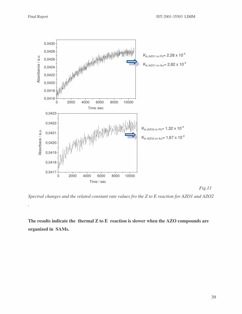
Fig.11
Spectral changes and the related constant rate values fro the Z to E reaction for AZO1 and AZO2
.
The results indicate the thermal Z to E reaction is slower when the AZO compounds are
organized in SAMs.
0 2000 4000 6000 8000 100000,0416
0,0418
0,0420
0,0422
0,0424
0,0426
0,0428
0,0430
A
bsor
banc
e / a
.u.
Time /sec
K� (AZO1 on Pt)= 2,28 x 10⁻⁴ K� (AZO1 on Au)= 2,82 x 10⁻⁴
0 2000 4000 6000 8000 100000,0417
0,0418
0,0419
0,0420
0,0421
0,0422
0,0423
Abs
orba
ce /
a.u.
Time / sec
K� (AZO2 on Pt)= 1,32 x 10⁻⁴ K� (AZO2 on Au)= 1,67 x 10⁻⁴

Final Report IST-2001-35503 LIMM
40
WP3 : Molecular movement in solution and sol-gel
Strategies For Placing Molecules in Specified Regions
P6 has developed three one-step methods to synthesize hybrid nanostructured silica thin films in
which a desired molecule is deliberately placed in a specified region of the nanostructure. These
strategies are succinctly termed "philicity" (or like dissolves like), “chemical bonding”, and
“bifunctionality”. The three strategies can be applied generally toward the incorporation of
organic, inorganic and biomolecules in selected regions of nanoostructured sol-gel thin films. The
synthesis conditions must be carefully developed in order to avoid disruption of the long range
order.
Philicity exploits the physical affinities of the active ingredients for a particular
environment (for example, that of a lipophilic dye for surfactant micelles) to place the molecule in
the desired region. Both lipophilic molecules (resulting in placement in the micelle) and
hydrophilic molecules (resulting in placement in the ionic region or pores in the framework) can
be used. The former is used with the azobenzene molecules. Bonding involves the use of
functional groups on the molecule that will chemically bond to the desired region. For example,
alkoxysilane groups that surround each molecule in three dimensions and will form the silicate
network during condensation. This strategy is not used with the azobenzene molecules directly,
but it will be used to place molecules such as photosensitizers spatially separated from but in
proximity to the azobenzenes. Bifunctionality requires that the molecule possess two different
groups that simultaneously interact with two different regions of the nanostructure. The most
important examples are azobenzene molecules that are derivatized with a condensable
alkoxysilane group on one end because these molecules can then chemically bond to the silicate
pore wall but position the active azobenzene group in the interior of the pore.
All of the nanostructured sol gel silica films used in the studies of light induced molecular
motion have a 2-d hexagonal structure that is templated by using 3.5 wt % CTAB in the final sol.
All of the films show x-ray diffraction patterns with peaks at 2θ values of 2.2 ± 0.1 and 4.4 ± 0.1
degrees, with a lattice spacing of approximately 3.9 nm.
Nanostructured Films Containing Derivatized Azobenzene Molecules

Final Report IST-2001-35503 LIMM
41
Specific Derivatized Azobenzenes The two azobenzene molecules that have been encapsulated in
nanostructured films are shown in figure 1. The
molecules are used without further derivatization when
the philicity strategy is employed. They are further
derivatized with a trialkoxysilane group as shown in
figure 2 when the bifunctionality strategy is employed.
Nanostructured Film Preparation The first step in the
preparation of the bifunctional film is to derivatize the
azobenzene with a triethoxysilane. 13. 4 ml of
isocyanatopropyltriethoxysilane is added to 28 mg of
the azobenzene that has been dissolved in dry
dichloromethane. The solution is refluxed for 3 hours.
Next 5 ml of stock solution (TEOS: EtOH: H2O: HCl (1:4:16:8 x 10⁻⁴) heated and stirred at 70°C
for and 1.5
Azobenzene Derivatives
N N OH
HO
MW: 228.25 g/mol
N N O
HO
O
OMW: 530.61 g/mol
FIGURE 4
Azobenzene Derivatives
N N OH
HO
MW: 228.25 g/mol
N N OH
HO
MW: 228.25 g/mol
N N O
HO
O
OMW: 530.61 g/mol
N N O
HO
O
OMW: 530.61 g/mol
FIGURE 4
Figure 1

Final Report IST-2001-35503 LIMM
42
hours), 0.2 ml of deionized water, 0.6 ml of HCl and 11. 6 ml of ethanol are stirred for 15 minutes.
The derivatized azobenzene solution is then added to the stock solution and stirred for another 15
minutes. 3.5 wt% CTAB is added and stirred until it is dissolved. Films are pulled from this final
solution. The 2D-hexagonal structure is confirmed by x-ray diffraction of the films.
The other films are prepared by stirring 5 ml of stock solution, 0.2 ml of deionized water,
0.6 ml of HCl and 10.6 ml ethanol, 28 mg of azobenzene and, 1ml of dichloromethane for 15
minutes. Amorphous films are then pulled from this solution. Then 3.5 wt% CTAB is added to
the solution with stirring until the surfactant is dissolved. Hexagonal structured films are then
pulled from this final sol. The 2D-hexagonal structured is confirmed by x-ray diffraction of these
films.
Spectroscopic Studies of Light Induced Molecular Motion in Nanostructured Films
Preparation of Films5 ml of stock solution
0.2 ml DI water0.6 ml .07 N HCl
11.6 ml EtOH
1.
2.
3.
13.4 µl of isocyanopropyltriethoxysilane +28 mg of azobenzene derivative
3hrsdry CH2Cl2
N
Me
Me
Me
Br-
3.5wt% CTAB
SOLN N O
O O
O
O
(CH2)3N(EtO)3Si
FIGURE 5
Preparation of Films5 ml of stock solution
0.2 ml DI water0.6 ml .07 N HCl
11.6 ml EtOH
1.
2.
3.
13.4 µl of isocyanopropyltriethoxysilane +28 mg of azobenzene derivative
3hrsdry CH2Cl2
N
Me
Me
Me
Br-
3.5wt% CTAB
SOLN N O
O O
O
O
(CH2)3N(EtO)3Si
FIGURE 5 Figure 2
Final Report IST-2001-35503 LIMM
43
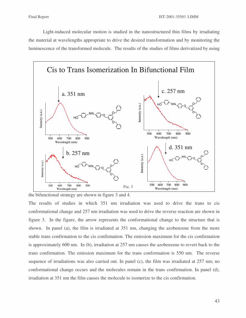
Light-induced molecular motion is studied in the nanostructured thin films by irradiating
the material at wavelengths appropriate to drive the desired transformation and by monitoring the
luminescence of the transformed molecule. The results of the studies of films derivatized by using
the bifunctional strategy are shown in figure 3 and 4.
The results of studies in which 351 nm irradiation was used to drive the trans to cis
conformational change and 257 nm irradiation was used to drive the reverse reaction are shown in
figure 3. In the figure, the arrow represents the conformational change to the structure that is
shown. In panel (a), the film is irradiated at 351 nm, changing the azobenzene from the more
stable trans confirmation to the cis confirmation. The emission maximum for the cis confirmation
is approximately 600 nm. In (b), irradiation at 257 nm causes the azobenzene to revert back to the
trans confirmation. The emission maximum for the trans conformation is 550 nm. The reverse
sequence of irradiations was also carried out. In panel (c), the film was irradiated at 257 nm; no
conformational change occurs and the molecules remain in the trans confirmation. In panel (d),
irradiation at 351 nm the film causes the molecule to isomerize to the cis confirmation.
Inte
nsity
(a.u
.)
900800700600500Wavelength (nm)
Inte
nsity
(a.u
.)
900800700600500Wavelength (nm)
Inte
nsity
(a.u
.)
900800700600500Wavelength (nm)
Inte
nsity
(a.u
.)
900800700600500Wavelength (nm)
c. 257 nm
d. 351 nm
a. 351 nm
b. 257 nm
N NO
O
O
HO
N NO
O
O
HO
NN OO
OHO
NN OO
OHO
Cis to Trans Isomerization In Bifunctional Film
FIGURE 6
Inte
nsity
(a.u
.)
900800700600500Wavelength (nm)
Inte
nsity
(a.u
.)
900800700600500Wavelength (nm)
Inte
nsity
(a.u
.)
900800700600500Wavelength (nm)
Inte
nsity
(a.u
.)
900800700600500Wavelength (nm)
c. 257 nm
d. 351 nm
a. 351 nm
b. 257 nm
N NO
O
O
HO
N NO
O
O
HO
NN OO
OHO
NN OO
OHO
Cis to Trans Isomerization In Bifunctional Film
FIGURE 6Fig. 3

Final Report IST-2001-35503 LIMM
44
The results of studies in which 351 nm irradiation was used to drive the trans to cis
conformational change and 457 nm irradiation was used to drive the reverse reaction are shown in
figure 4. In panel (a), the film is irradiated at 351 nm, changing the azobenzene to the cis
conformation. The emission maximum for the cis conformation is at approximately 600 nm. In
panel (b), irradiation at 457 nm causes the azobenzene to revert back to the trans conformation
with its emission maximum at 550 nm. The reverse sequence of irradiations was also carried out.
In panel (c), the film was irradiated at 457 nm, no change occurs, and the molecule remains in its
trans conformation. Finally, in panel (d), irradiation at 351 nm the film causes the molecule to
isomerize to the cis conformation.
Inte
nsity
(a.u
.)
800700600500Wavelength (nm)
Inte
nsity
(a.u
.)
800700600500Wavelength (nm)
Inte
nsity
(a.u
.)
800750700650600550500Wavelength (nm)
N NO
O
O
HO
N NO
O
O
HO
NN OO
OHO
NN OO
OHO
Cis to Trans Isomerization In Bifunctional Film
d. 351 nm
a. 351nm
b. 457 nm
c. 457 nm
Inte
nsity
(a.u
.)
800700600500Wavelength (nm)
FIGURE 7
Inte
nsity
(a.u
.)
800700600500Wavelength (nm)
Inte
nsity
(a.u
.)
800700600500Wavelength (nm)
Inte
nsity
(a.u
.)
800750700650600550500Wavelength (nm)
N NO
O
O
HO
N NO
O
O
HO
NN OO
OHO
NN OO
OHO
Cis to Trans Isomerization In Bifunctional Film
d. 351 nm
a. 351nm
b. 457 nm
c. 457 nm
Inte
nsity
(a.u
.)
800700600500Wavelength (nm)
FIGURE 7Fig. 4

Final Report IST-2001-35503 LIMM
45
Movement of molecules through evacuated pores
Experiments were carried out to determine if light-induced azobenzene isomerization could be
used to move molecules through the pores of 2-D hexagonal film as shown in the drawing below.
The strategy is schematically illustrated in the scheme below. First we fill the empty pores with a
luminescent probe, then we stimulate the azodendrimer with light and monitor the motion of the
probe by observing a decrease of luminescence intensity in irradiated regions
The experiment used our solvent extracted 2-D hexagonal films backfilled with a laser dye (LDS
821) as the movable molecule. This molecule was chosen because laser dyes are intensely
luminescent This molecule has a λmax around 650 nm and an emission maximum at approximately
730 nm. This emission is in the red and does not interfere with the aggregate emission from the
azodendrimer.
Using a diaphragm and focusing lens, we produced a laser spot about 250 microns in diameter.
Constants were laser power (kept at 10mW), slit width (200 micron), distance between focusing
lens and sample (at 37.5cm), integration time (1s), and temperature (40K). We then excited with
351 and 457 nm and collected spectra at various locations on film.
Figure 5. Normalized laser dye emission intensity as a function of irradiation time
1.0
0.8
0.6
0.4
0.2
0.0
inte
nsity
9000850080007500700065006000wavelength (A)
1.0
0.8
0.6
0.4
0.2
inte
nsity
9000850080007500700065006000wavelength (A)
----initial ----40 minutes ----60 minutes 351 nm excitation
----initial ----40 minutes ----60 minutes 457 nm excitation

Final Report IST-2001-35503 LIMM
46
Shown in figure 5, the laser dye emission intensity decreases over time. Each spectra took
approximately 20 minutes to collect so the total irradiation time was about 1 hour. With excitation
at 351 nm we observed a 70% decrease in laser dye intensity after irradiation for 40 minutes and a
90% decrease after 1 hour. Exciting at 457 nm, a 40% decrease was observed after 40 minutes of
irradiation and a 50% decrease after 1 hour.
As a control we irradiated an underivatized solvent-extracted film, which showed no loss
of laser dye intensity over the same period of time (see fig. 6). The film was prepared and
irradiated in the same manor as the derivatized film and eliminated thermal heating or
photobleaching of the laser dye as the cause of the decrease in luminescence.
As another control we irradiated an azodendrimer derivatized film with 647 nm light. This
wavelength excites the laser dye but is too low in energy to excite the cis/trans isomerization of
the azobenzene (see fig. 7a-b). A slight decrease in laser dye intensity was observed, but not of
the same magnitude with excitation at 351 or 457 nm. The laser dye intensity decreased by 13%
after 40 minutes of irradiation and to 30% after 1 hour.
-----initial -----40 minutes -----60 minutes
2.0
1.5
1.0
0.5
0.0
A.U
.
800700600500400300wavelength (nm)
a
Figure 6. Underivatized, solvent-extracted film irradiated at 457 nm. Approximate irradiation time is 1 hour.
15
10
5
0
x10
3
900085008000750070006500wavelength (A)
1.0
0.8
0.6
0.4
0.2
inte
nsity
90008500800075007000wavelength (A)
b -----initial -----40 minutes -----60 minutes

Final Report IST-2001-35503 LIMM
47
In addition, we have studied the mobility of R6G molecules inside G0, G1, G2 and G3
bifunctional films. In this way we determined whether the distribution of the dyes after photo-
isomerisation is static or dynamic and, in the latter case, how dynamic the system is. We have
investigated the influence of the amount of ethanol (solvent for R6G) on the mobility and
displacement of the dye.
Methods:
The mobility was studied by filling and leaching experiments using steady-state fluorescence. In
addition, fluorescence recovery after photobleaching (FRAP) was performed with our confocal
fluorescence lifetime microscope and argon ion laser (514 nm). In this method the fluorophores in
a small spot are photobleached for a short time using a high laser intensity. Subsequently,
fluorescence is recovered due to diffusion of the fluorophores, which is observed using the same
laser at a 103 �104 × lower intensity.
Results:
The results obtained by the filling and leaching experiments indicate high mobility within the
nanotubes. The filling experiments showed that the G0 film is filled to reach an equilibrium
concentration within ~ 10 min (see Fig. 8). However, due to the short rinsing steps applied after
each filling period – which were necessary in order to remove superficial dye – the scatter in the
filling data was high. It should also be noted that the filling of empty films is due to capillary
action for which the speed may be quite different than for diffusion.
Figure 7a: Absorption spectra of azodendrimer; 6b: emission spectra of azodendrimer derivatized film with excitation at 647 nm.
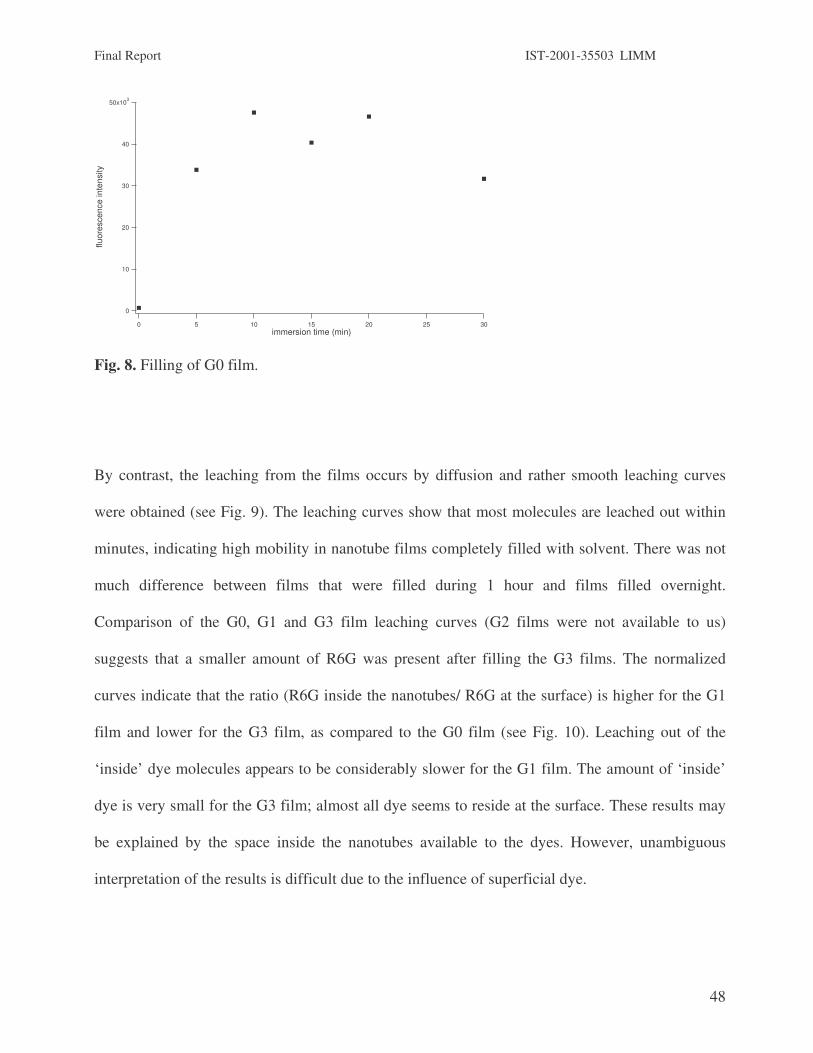
Final Report IST-2001-35503 LIMM
48
50x103
40
30
20
10
0
fluor
esce
nce
inte
nsity
302520151050immersion time (min)
Fig. 8. Filling of G0 film.
By contrast, the leaching from the films occurs by diffusion and rather smooth leaching curves
were obtained (see Fig. 9). The leaching curves show that most molecules are leached out within
minutes, indicating high mobility in nanotube films completely filled with solvent. There was not
much difference between films that were filled during 1 hour and films filled overnight.
Comparison of the G0, G1 and G3 film leaching curves (G2 films were not available to us)
suggests that a smaller amount of R6G was present after filling the G3 films. The normalized
curves indicate that the ratio (R6G inside the nanotubes/ R6G at the surface) is higher for the G1
film and lower for the G3 film, as compared to the G0 film (see Fig. 10). Leaching out of the
‘inside’ dye molecules appears to be considerably slower for the G1 film. The amount of ‘inside’
dye is very small for the G3 film; almost all dye seems to reside at the surface. These results may
be explained by the space inside the nanotubes available to the dyes. However, unambiguous
interpretation of the results is difficult due to the influence of superficial dye.

Final Report IST-2001-35503 LIMM
49
To study the mobility in more detail, FRAP was judged to be a suitable technique: it can be used
to obtain the diffusion coefficient, detect different locations (concerning diffusion) inside the film,
and show whether the films are continuous or not. In the last case, repeated FRAP will deplete the
available dye molecules in a closed volume, resulting in increasingly less recovery and loss of
fluorescence from the surroundings of the bleached spot.
We have obtained preliminary data suggesting fluorescence recovery within 15 min. and t1/2 values
(recovery half time) of a few minutes (see Fig. 11).
80x103
60
40
20
0
fluor
esce
nce
inte
nsity
150010005000rinse time (s)
Fig. 9. Leaching of R6G from overnight-filled G0 bifunctional film.

Final Report IST-2001-35503 LIMM
50
0
10
20
30
40
50
60
70
80
90
100
0 500 1000 1500 2000 2500
rinse time (s)
fluor
esce
nce
(cps
)
G0, overnight
G0, 65 min
G1, 65 min
G3, 65 min
4
3
2
1
0
Fluo
resc
ence
(cou
nts/
ms)
8006004002000time (s)
0.20.10.0
-0.1-0.2
low intensity bleaching corrected FRAP curve uncorrected FRAP curve
Fig. 10. Normalized leaching curves of G0, G1 and Fig. 11. Fluorescence recovery of R6G in G0 G3 films after 65 min. fill or overnight filling. bifunctional film.
Since photobleaching also occurs to some extent during measurement of the recovery, correction
of the FRAP curve with a low-intensity bleaching curve is required (Fig. 11). From the limited
amount of data available to us as yet we conclude that ethanol evaporates from the films
significantly within hours. This seems to reduce the mobility of R6G: slower fluorescence
recovery is observed. The reduced amount of ethanol may also reduce the mobile dye fraction.
This may – together with low-intensity bleaching – explain the observed incomplete fluorescence
recovery. In experiments addressing the continuity of the nanotube films these factors have to be
separated experimentally from the effect of depletion of available dye molecules.
Due to an instrumental problem with the laser FRAP experiments on G1 and G3 films had to be
postponed, but they will be carried out in the final weeks of the LIMM project.
Light Induced Molecular Movements
Confocal Scanning Laser Microscopy
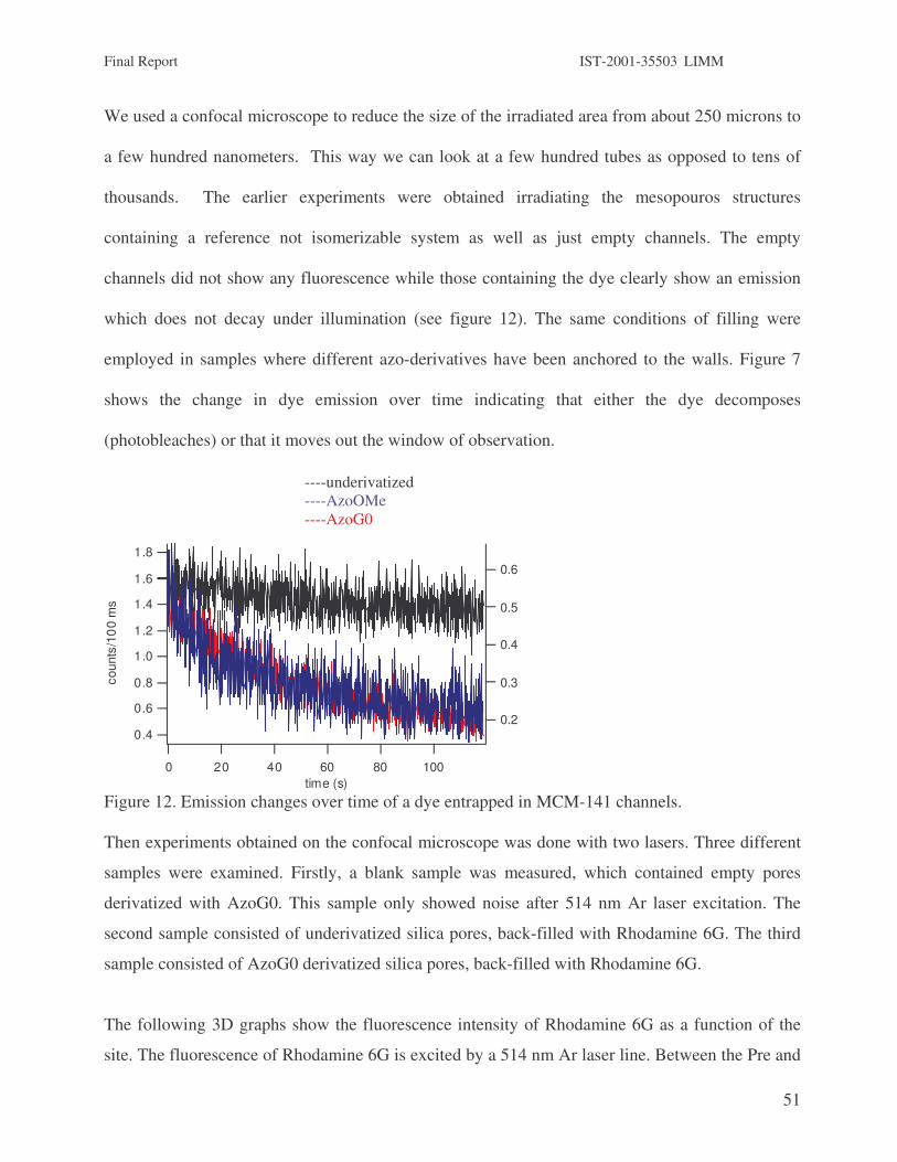
Final Report IST-2001-35503 LIMM
51
We used a confocal microscope to reduce the size of the irradiated area from about 250 microns to
a few hundred nanometers. This way we can look at a few hundred tubes as opposed to tens of
thousands. The earlier experiments were obtained irradiating the mesopouros structures
containing a reference not isomerizable system as well as just empty channels. The empty
channels did not show any fluorescence while those containing the dye clearly show an emission
which does not decay under illumination (see figure 12). The same conditions of filling were
employed in samples where different azo-derivatives have been anchored to the walls. Figure 7
shows the change in dye emission over time indicating that either the dye decomposes
(photobleaches) or that it moves out the window of observation.
Figure 12. Emission changes over time of a dye entrapped in MCM-141 channels. Then experiments obtained on the confocal microscope was done with two lasers. Three different
samples were examined. Firstly, a blank sample was measured, which contained empty pores
derivatized with AzoG0. This sample only showed noise after 514 nm Ar laser excitation. The
second sample consisted of underivatized silica pores, back-filled with Rhodamine 6G. The third
sample consisted of AzoG0 derivatized silica pores, back-filled with Rhodamine 6G.
The following 3D graphs show the fluorescence intensity of Rhodamine 6G as a function of the
site. The fluorescence of Rhodamine 6G is excited by a 514 nm Ar laser line. Between the Pre and
1.8
1.6
1.4
1.2
1.0
0.8
0.6
0.4
coun
ts/1
00
ms
100806040200time (s)
0.6
0.5
0.4
0.3
0.2
----underivatized ----AzoOMe ----AzoG0

Final Report IST-2001-35503 LIMM
52
Post measurements, a 438 nm diode laser line is focused on spot (X,Y) = (40,40) for 30 minutes.
Then again the 514 nm Ar laser line is used to excite the Rhodamine 6G and a specific surface is
analyzed. The figure of underivatized samples show that the 438 nm laser line at spot (40,40) does
not seem to influence the Rhodamine 6G fluorescence.
Underivatized R6G Pre Underivatized R6G Post
The next samples were derivatized with AzoG0 bound to the walls of the silica tubes. The same experiment is performed. That is first the fluorescence intensity of Rhodamine 6G as a function of site is recorded with a 514 nm Ar laser line excitation. Then, a 438 nm laser line is used to excite the AzoG0 at site (X,Y) = (40,40) for 30 minutes. Finally, again the Rhodamine fluorescence intensity as a function of site is analyzed using the 514 nm Ar laser line as excitation source.
AzoG0 R6G Pre AzoG0 R6G Post
The figure shows that in the case of AzoG0 derivatized silica nanotubes, the fluorescence intensity is much smaller than in the case of underivatized silica nanotubes. This can be explained by the much slower diffusion of R6G molecules into the channels caused by hindering AzoG0 molecules. Also we can see clearly the influence of the AzoG0 excitation. After the 438 nm excitation (where R6G does not absorb) at site (40,40) the R6G fluorescence intensity at this site is much lower than before the 438 nm excitation. There is even some increase in fluorescence intensity at certain areas around site (40,40). The change in fluorescence intensity is due to movement of the R6G molecules, which is induced by the AzoG0 photoisomerization. In summary, we believe we are seeing molecular motion in the pores of 2D hexagonal silica thin films due to the cis/trans isomerization of azodendrimers lining the pore wall.

Final Report IST-2001-35503 LIMM
53
WP4: Photo-controlled vectorial motion of azo-compounds for nano-scale patterning of thin polymeric films
I. Introduction and background.
One of the aim of the LIMM project was to demonstrate the possibility to control, with visible light, the motion of molecule in order to produce, on a surface or a thin film, artificial patterns with nanometric characteristic size. It is known since several years that polymeric films containing Dispersed-Red 1 (DR1) azobenzene derivatives exhibits spectacular photo-induced matter migration effects. When illuminating a thin film of such a material with a light of wavelength in the visible absorption band of the photochromic moieties, a topographic surface pattern is formed. This pattern shape is related to the light intensity and polarisation distribution. Fig.1 shows an example of a surface relief grating patterned on a 0.8�m-thick sol-gel film, containing DR1 units, under illumination with an interference pattern produced by two p-polarised laser beams of wavelength 532nm.
Fig.1 : Scanning electron microscopy image of a surface relief grating optically patterned on a 1�m-thick sol-gel film containing DR1 units by illumination with an interference pattern produced by two p-polarised laser beams of wavelength 532nm.
This phenomenon is directly related to the photoisomerisation of the photochromes. The azobenzene molecules may exist in two isomeric states, the trans and the cis states. The transition between these states can be induced by light absorption. Due to the electron donor and the electron acceptor terminating groups, the trans-state of the DR1 is stable and, when the molecule absorbs a photon and photo-isomerises into the cis-state, the thermal activation of the reverse transition is very efficient. This way, the photochromes undergoes a complete trans-cis-trans photoismerisation cycle (Fig.2).

Final Report IST-2001-35503 LIMM
54
Fig.2 : Scheme of the DR1 unit and of its trans-cis-trans photoisomerisation cycle.
The repetition of these photo-induced molecular conformation changes results in a motion of the photochromes. The direction of this motion appears to be defined by the light electric field and, when the light polarisation is perpendicular to the light intensity gradient (which is the case in the interferencs produced by p-polarised laser beams), the molecules move out from the bright regions and accumulate into the dark ones. The molecules being grafted to the matrix their motion induces a matter migration which results in the formation of a topographic pattern.
In the framework of the LIMM project, we have studied in details the properties and mechanisms responsible for photo-induced surface patterning in a hybrid material made of an inorganic silica matrix containing azobenzene units grafted to the polymeric backbone. We have developed a method, for optical nano-patterning of surface and thin films, which exploits the photo-controlled molecular motion of azobenzene moieties.
II. The material : thin sol-gel films containing azo-compounds The hybrid material under study is made of an inorganic silica gel containing the azobenzene unit grafted to the polymeric backbone. The sol-gel samples are prepared from functionalized alkoxysilane monomers bearing a spacer unit and an electron-donor/electron-acceptor substituted azobenzene. The role of the spacer is to prevent against photochromic molecule aggregation. For the purpose of our study, different spacers and azobenzene derivatives have been synthesised. The synthesis and characterisation of the materials obtained with these different species are described below. However, most of the optical patterning experiments have been performed on a "reference" material which turns out to exhibit optimised properties with respect to the concerned application. II.1. The photochromic material synthesis - The reference system : Si-DR1 / Si-K.
The reference material that we have synthesised and studied contains DR1 (Dispersed Red 1) as azobenzene unit and carbazole as spacer unit. The first step of the synthesis is the functionalisation of the DR1 and of the carbazole with tetraethoxysilane (Fig.3). This is necessary for grafting the molecules onto the silica matrix.

Final Report IST-2001-35503 LIMM
55
O
NH Si
OCH2CH3
OCH2CH3
OCH2CH3
ICPTEOSNN
NO2NOH
NN
NO2N
O
THF/Sn
N
O
NH
Si(OEt)3
N
O
cl
APTES
Pyridine
Fig.3 : Scheme of the synthesis of Si-DR1 and Si-K units of the reference system.
The sol-gel samples are then prepared from the functionalised alkoxysilane monomers Si-DR1 and Si-K. To obtain solid-state materials, the functionalised monomers are copolymerised (Fig.4) with a cross-linking agent, the tetraethoxysilane (TEOS). In a typical sol preparation, alkoxysilanes (2 Si-DR1 + 4 Si-K + 1 TEOS) are dissolved in tetrahydrofuran and hydrolyzed with acidic water ([H2O]/[Si] = 4). The mixture is stirred for several hours, then pyridine is added to neutralise the medium and enhance therefore the condensation reaction rate.
N
R
Si
OO
O
Si
HO
O
O
Si
O
O
R
Si
O
OR
Si
R
O
SiOH
R'O N
N
N
NO2
N
N
N
NO2
O
O
HN
Si
OEt
OEtOEt
OEt
SiEtO OEt
OEt
N
NH SiOEt
OEtOEt
O
Fig.4 : Scheme of the co-polymerisation reaction
Afterwards, the so-prepared hybrid sol is deposited by spin-coating on a glass substrate, leading to a hybrid film of thickness that can be varied from 20 nm to 800 nm by adjusting the sol concentration and the angular velocity of the spin coater (Fig.5). Samples are not heat treated in order to keep a low condensation degree (weakly cross-linked silica network).

Final Report IST-2001-35503 LIMM
56
Fig.5 : Pictures of photochromic sol-gel films of different thicknesses spin-coated on a glass substrate. The absorption spectrum exhibits a broad band in the visible range which is due to the DR1.
The absorption spectrum of a Si-DR1/Si-K/TEOS hybrid film exhibits a broad band in the wavelength range between 400 nm and 600 nm. This absorption band is due to the azobenzene moieties. Under illumination in this spectral range, the photo-isomerisation of the DR1 molecules from the trans configuration (stable state) to the cis state (metastable state) is excited. The reverse cis-to-trans transition is thermally activated.
II.2. Details of the organic synthesis of the precursors
II.2.1. General strategy
In order to obtain functionalized systems (azodyes covalently linked to the polymer backbone via a linker chain), we have prepared chromophores bearing free hydroxyl, vinylic or allylic endgroups. The silylated precursors are organic molecules that have been chemically modified to provide alkoxysilane functionality. This allows the silane modified molecules to participate in the hydrolysis and condensation reactions, similarly to other usual alkoxide precursors. To prepare these compounds, different molecular species (hereafter noted R) were modified using the initial sol-gel precursors shown in Fig.6.
2HN
Si(OEt)3
N
Si(OEt)3
COHSi
Cl
ClCl
HSi
Cl
ClMe
ICPTEOS APTES TCLS MDClS
Fig.6 : Precursors used for the sol-gel functionalization of the molecules.
Three types of reactions were used to functionalize these molecules (Fig.7) :

Final Report IST-2001-35503 LIMM
57
- hydrosilylation between an allyl or vinyl-terminated molecule R and the methyl-dichlorosilane (MDClS) or the trichlorosilane (TClS), which results in a C-Si bond ;
- addition of an hydroxyl-terminated molecule R on the 3-(isocyanatopropyl)triethoxysilane (ICPTEOS) which results in a carbamate link ;
- amidation of an acyl chloride-terminated molecule R using the 3-(aminopropyl)-triethoxysilane (APTES).
R
R Si(OEt )3
R
OH
R
O
O
NH
Si(OEt)3
R
O
R
O
NH
Si(OEt )3
Cl
2) NEt3/ETOH
ICPTEOS
Sn Catalyst
APTEOS
Benzene/pyridine
1
2
3
R Si(OEt )2
Me1) HSiMeCl2
1) HSiCl3
THFPt/C
Fig.7. Strategy for the sol-gel functionalisation of the molecule.
In the case where the R-group is the azo-dye chromophore, functionnalization was
achieved by reacting the chromophores bearing free hydroxyl groups with 3-isocyanatopropy triethoxysilane, or by coupling an aniline derivatives bearing one or two allylic groups with a diazonium salt, on which an alkoxysilane part is then added for coupling purposes. Many azobenzenes derivatives were synthesised and functionnalized in that way (Fig.8). The obtained molecules maybe differentiated by two characteristics : the number of grafting sites (3 or 6), and the length of the linker to the matrix (Si-C or carbamate linkage).

Final Report IST-2001-35503 LIMM
58
NH3C
NN
NO2
NHH3C
NH3C
BrK2CO3/DMF
O2N N2+ 1) HSiCL3
2) ETOHAcOH/AcOK
N
NN
NO2
N
NN
NO2
NHH3C
NK2CO3/DMF
O2N N2+ 1) HSiCL3
2) ETOHAcOH/AcOK
Br
Si(OEt)3Si(OEt)3
N
NN
NO2
H3C
Si(OEt)3
Fig.8 : Synthesis scheme for the units with three and six grafting sites through a Si-C linkage.
In the case where the R-group is the spacer used to prevent chromophore aggregation, the
functionalized alkoxysilane monomers bearing bulky molecules such as a carbazole were attached via a flexible linker chain by reacting carbazole-9-carbonyle chloride with amino-propyltriethoxysilane (APTES), yielding the molecular precursor Si-carbazole (Si-K). Different silylated precursors containing other bulky molecules such as anthracene or naphthalene, were also prepared (Fig.9) by reacting the corresponding free alcohols with the 3-isocyanato-propyltriethoxysilane. Bis trimethoxysilylbenzene precursor have been obtained by reacting 1,4-dibromobenzene with chlorotrimethoxysilane in the presence of magnesium and THF.

Final Report IST-2001-35503 LIMM
59
O
O
NH
Si(OEt)3
N
O
NH
Si(OEt)3
Si-Carbazole Si-Anthracene
O
O
NH
Si(OEt)3
Si(OEt)3(EtO)3Si
Si-Naphtalene Phenyl-ditriethoxysilane
Fig.9 : The four units with three grafting sites used as spacers in the photochromic materials.
II.2.2. Experimental details of the general synthesis process
Preparation of Aniline derivatives Under Nitrogen, N-Methylaniline or Aniline is dissolved in distilled DMF with 2
equivalents of potassium carbonate (K2CO3). Two equivalents of allylbromide are added dropwise while stirring at 50°C. After one night, excess K2CO3 is eliminated by filtration and DMF is evaporated in vacuum. The resulting products, N-allylmethylaniline or diallylaniline, is used in the next step without further purification.
Coupling with a diazonium salt P-Nitrophenydiazonium tetrafluoroborate salt is dissolved at 0°C in a mixture of distilled
water and acetic acid (50/50 (v/v)). One equivalent of N-allyl-Methyl aniline or diallyl aniline in an acetic acid solution is added dropwise at room temperature, with 2 equivalents of potassium acetate. A red precipitate appears, coming from the “azo” species. After 30mn, the solution is poured into water and the products are collected by filtration and can be recristallized in cyclohexane. The allyl-end diazo can be then hydrosilylated in another step.
Coupling by Hydrosilylation Into a stirred solution of the appropriate allylic compound (n mole) in dry THF, were
added 2n mole of MDClS or of TClS and 2% of dried platinum catalyst. The mixture was stirred for 12 hours at room temperature. Excess of chlorosilane was removed under vacuum, and the air sensitive solid obtained was stored under nitrogen. Then, it was used subsequently in the next step without further purification.
Then, dry THF was added to the chlorosilane derivative, and 5n mole of triethylamine was added dropwise. Once the addition was complete, the solution was cooled and 5n mole of ethanol was added. The reaction mixture was stirred for two hours at room temperature and the obtained solid is filtered. The solvent is removed at reduced pressure to leave diethoxy or triethoxysilane derivatives. The compounds were isolated by flash chromatography and /or recrystallisation.

Final Report IST-2001-35503 LIMM
60
Coupling with the 3-isocyanatopropyltriethoxysilane ( ICPTEOS). Into a stirred solution of the appropriate alcohol (n mole) in anhydrous tetrahydrofurane
and a few drops of dibutyltindilaurate catalyst,was added ICPTEOS (1,05n mole) under nitrogen atmosphere. The mixture was stirred for 4 to 6 hours and then the solvent was removed. Finally, the compounds were purified by flash chromatography using silicagel or by re-crystallisation.
Preparation of Si-carbazole Into a stirred solution of acyl carbazole ( 0.0035 mole) in 10 ml of anhydrous benzene and
2ml of pyridine was added APTES (0.0038 mole) in 10ml of benzene and stirring was maintained for 1 hour at room temperature. The mixture was filtered and the solvent was removed. The crude was purified by flash chromatography eluting with ethyl acetate and cyclohexane (20:80 v/v) and finally re-crystallised twice from cyclohexane yielding 81% of white needles.
II.3. Characterisation of the material
II.3.1. The interaction between photoactive molecules : the role of the spacer unit.
One of the crucial feature of the photochromic materials synthesis is the control of the interactions between the photoactive species. In particular, it is important to avoid molecule aggregation. As mentioned above, the approach that we have developed consists in introducing, in the host matrix, a spacer unit which does not exhibit any optical activity but screens the dipolar interactions between azobenzene molecules.
The synthesis that we have developed is based on the use of the carbazole Si-K moieties (reference material), with a molecular concentration ratio [Si-K]/[Si-DR1] = 2. In fact, the exact role of the Si-K unit is not completely identified, neither in the synthesis process, nor in the photo-induced matter migration effect. In order to start answering these questions and to optimise the material synthesis, we have explored the use of other possible spacer units of with chemical nature and different sterical size. Four types of molecules have been synthesized (see section 1.1.1.a) which can all be grafted to the silica network and which exhibit various number of phenyl-group : the Si-carbazole, the Si-anthracene (3 phenyl groups), the Si-naphtalene (2 phenyl groups) and the phenyl-ditriethoxysilane (1 phenyl group).
For each of the spacer units, we have elaborated sol-gel films containing DR1-photoactive molecule. As can be seen from the absorption spectra, all measured on films of 400 nm thickness and from the AFM images of the film surface (Fig.10), no dimerisation or aggregation of the Si-DR1 are observed when using Si-carbazole, Si-anthracene, Si-naphtalene as spacer unit, with the same concentration ratio [spacer]/[Si-DR1] = 2. Moreover, photo-induced matter migration has been observed with similar efficiency (see section 3 of the present report).

Final Report IST-2001-35503 LIMM
61
S i
S i
O E t O E t
O E t
O E tO E t
O E t
phenyl-ditriethoxysilane
300 350 400 450 500 550 600 650 7000,0
0,5
1,0Absorbance
wavelength (nm)
O
O
HN
Si
OEt O
Et
OEt
0,0
0,5
1,0
300 350 400 450 500 550 600 650 700
Absorbance
wavelength (nm)
Si-naphtalene
O
O
HN
SiO
Et OEt
OEt
0,0
0,5
1,0
300 350 400 450 500 550 600 650 700
Absorbance
wavelength (nm)
Si-anthracene
N
NH Si
OEt
OEt
OEt
O
0,0
0,5
1,0
300 350 400 450 500 550 600 650 700
Absorbance
wavelength (nm)
Si-carbazole
grey scale : 30nmscan size : 5µm
grey scale : 5nmscan size : 5µm
grey scale : 2nmscan size : 5µm
grey scale : 5nmscan size : 5µm
Fig.10 : Schemes of the four spacer units used for photochromic material synthesis together with the corresponding absorption spectra and AFM images measured on thin films.
On the contrary, when using the phenyl-ditriethoxysilane (Ph-diTEOS), the quality of the films with respect to the optical properties (absorption spectrum) and to the surface roughness is very poor. In particular, AFM images show holes and molecule aggregates. These features are observed even when using larger concentration ratio [Ph-diTEOS]/[Si-DR1] = 4 and the concentration of the Si-DR1 molecules can not be as high as in the films using the other spacer units. We conclude that the use of the single phenyl group as spacer does not allow reliable materials synthesis.
II.3.2. The degree of polymerisation of the host-matrix.

Final Report IST-2001-35503 LIMM
62
The degree of polymerisation of the sol-gel matrix mainly depends on three parameters :
- The material ageing,
- The thermal treatments performed on the deposited films,
- The concentration ratio between the cross-linking agent (TEOS) and the spacer unit.
Experiments performed on aged films show that, after several months at room temperature, films are stable and the light-induced matter migration still occurs with a similar efficiency.
When the materials are heat-treated at 110°C for several hours, just after deposition, the photoisomerisation still occurs, but the matter migration is significantly slown down.
Higher concentration ratio [TEOS]/[Si-K] increases the cross-linking of the polymeric silica network without changing the concentration of the film in Si-DR1 units. We have synthesised films with three different alkoxysilanes compositions:
- 1 Si-DR1 + 5 Si-K + 1 TEOS
- 1 Si-DR1 + 4 Si-K + 2 TEOS
- 1 Si-DR1 + 2 Si-K + 4 TEOS
The atomic force microscopy (AFM) images of corresponding films of 140nm thickness are shown in Fig.11, together with the absorption spectra. In the three cases, the quality of the films is very good : the roughness of the surface is of a few nanometer and no molecule aggregation is detected, neither from the AFM image nor from the absorption spectra.
400 500 600 7000,00,10,20,30,40,50,6 Absorbance
wavelength (nm)400 500 600 700
0,00,10,20,30,40,50,6
wavelength (nm)
Absorbance
400 500 600 7000,00,10,20,30,40,50,6
wavelength (nm)
Absorbance
1 Si-DR1 + 5 Si-K + 1 TEOS
grey scale : 2 nmscan size : 5 µm
1 Si-DR1 + 4 Si-K + 2 TEOSgrey scale : 2 nmscan size : 5 µm
1 Si-DR1 + 2 Si-K + 4 TEOSgrey scale : 2 nmscan size : 5 µm
Figure 11 : AFM images of 140nm-thick films and absorbance spectra of 400nm-thick films prepared with different alkoxysilanes concentrations.

Final Report IST-2001-35503 LIMM
63
A more detailed study of the degree of polymerisation of the matrix is of course of interest. But it is difficult to obtain quantitative data on the light-induced matter migration phenomena. However, this could be achieved by performing systematic patterning experiments with the interference techniques (see section IV). These measurements are now in progress.
II.2.3. The interaction between the photoactive molecules and the matrix : influence of the number of grafting sites.
The interactions between the photoactive units and the matrix mainly depend on :
a) the number of grafting sites,
b) the length of the linker chain.
We have synthesised sol-gel films with six azobenzene molecules (listed below) following the process described in section 1. In these synthesis, the alkoxysilane molar composition is 2 DR1 + 4 Si-K + 1 TEOS, which corresponds to a DR1 molar concentration of 28 %.
- DR1 with 0-grafting chain : DR1-0 (commercial DR1 dispersed in the matrix)
NNNO2N O H
- DR1 with 1-grafting long chain to the silica backbone : Si-DR1-1L (reference chromophore)
O
NH Si
OCH2CH3
OCH2CH3
OCH2CH3
NNNO2N
O
- DR1 with 1-grafting short chain to the silica backbone : Si-DR1-1S
NCH3
NNO2N
Si
OEt OEt
OEt
- DR1 with 2-grafting long chains on the same benzene ring : Si-DR1-2L
NNNO2N
OO
NH SiOEt
OEtOEt
OO
NH SiOEt
OEtOEt
- DR1 with 2-grafting short chains sites on the same benzene ring : Si-DR1-2S
NNNO2N
Si
Si
OEt
OEt
OEt
OEt
OEtOEt

Final Report IST-2001-35503 LIMM
64
a) The number of grafting sites.
When the molecules are not grafted onto the matrix (DR1-0), it is not possible to obtain homogeneous films since a strong molecule aggregation occurs and leads to the formation of DR1 crystallites. This is evidenced when comparing the AFM images of 140nm-thick films prepared with the DR1-0 units and with the DR1-1L units (Fig.12). Then, it appears that the elaboration of a material containing a high concentration of non-grafted azobenzene units which are free to diffuse inside the matrix is a difficult task.
NN
NO2N OH
20 µm 5 µm
NN
NO2NO
O
NH Si
OEt
OEt
OEt
Fig.12 : AFM images of 140nm-thick sol-gel films prepared with non-grafted (left image) and grafted (right image) azobenzene units.
We have also synthesised films with DR1 molecules grafted to the matrix through two linker chains. The multiple sites grafting of azo-units onto a silica sol-gel matrix is of great interest for light-controlled movement in confined liquid phases and sol-gel films (WP3). The quality of the films that we have obtained is satisfactory with respect to the optical properties (absorption, homogeneity) and to the surface roughness (less than 2nm). Nevertheless, defects are observed on the AFM image (left image of Fig.13) which are not seen on the reference material films prepared with Si-DR1-1L azobenzene units grafted with only one linker chain to the matrix (right image of Fig.13). These defects may occur during the deposition of the film. Experiments are in progress to identify the origin of these defects.

Final Report IST-2001-35503 LIMM
65
O
NH Si
OCH2CH3
OCH2CH3
OCH2CH3
NNNO2N
O
5 µm
NNNO2N
OO
NH SiOEt
OEtOEt
OO
NH SiOEt
OEtOEt
5 µm
Figure 13 : AFM images of 140nm-thick sol-gel films prepared with grafted Si-DR1 units through two linker chains (left image) and a single linker chain (right image).
b) The length of the linker chain.
We have prepared sol-gel films containing photoactive molecules with a short chain linkage between the optical group and the silicate matrix (Si-DR1-1S). The quality of the films was comparable with those containing Si-DR1-1L i.e. without any molecular aggregation as can be seen from the AFM image and the absorption spectrum of Fig.14. Optical measurements on these films are now in progess to quantify and to evidence the influence of the length of the linker chain on the molecule photoisomerisation and on the matter migration efficiency.
350 400 450 500 550 600 650 7000
0.2
0.4
0.6
0.8
1
1.2 Absorbance
wavelength (nm)
NCH3
NNO2N
Si
OEt OEt
OEt
Figure 14 : Absorption spectrum and AFM image of a sol-gel film prepared with Si-DR1 units grafted to the matrix through a short linker chain (Si-DR1-1S).
III. Photo-controlled nano-patterning of azo-hybrid films. III.1 The near-field experimental set-up for optical nanopatterning
The experiment that we have developed for the optical nanopatterning of photochromic sol-gel films is based on an aperture near-field optical microscope. This instrument has two main characteristics :
- the near-field light source of nanometric size, which is the aperture at the tip of a metallised tapered optical fiber ;
- the control of the tip-to-sample distance by shear-force techniques, which allows to measure, in-situ with the same tip, the topography of the surface with nanometric resolution.

Final Report IST-2001-35503 LIMM
66
III.1.1 The near-field nanosource. The nanometric light source is produced by an original procedure which combines laser-heated pulling, acid etching and metallisation of a single-mode fibre with core and cladding diameters of 3.7 µm and 125 µm respectively (Fig.15). The fibre pulling is carried out with a home-made apparatus which uses a CO2 laser as heating source. The laser is operated in a pulsed mode so that the fibre undergoes a sequence of heating-pulling-cooling cycles. After each cycle the diameter of the tip is reduced by a controlled quantity of the order of 1µm. The whole sequence ends up by a last laser shot which produces a conical tip, with a cone angle of about 50° and a flat aperture of diameter varying from 400 nm to 1000 nm. The second step consists of a short chemical etching of the pre-formed tip with 25% aqueous hydrofluoric acid at a temperature of 0°C. We made sure that the chemical etching is isotropic and maintains the taper angle while the diameter of the flat aperture is
reduced. Finally, the etched fibre is coated with a 10 nm-thick chromium layer and a 100 nm-thick aluminium layer, by evaporation in a vacuum chamber. The geometry of the rotating fibre holder device that we have conceived allows to keep open the tip aperture which size is defined by the preceding chemical etching. When light is injected into the fibre, the outcoming light is confined by the metal coating at the tip aperture (Fig.16). This process allows to produce routinely optical nanosources of 50 nm typical diameter, i.e. much smaller than the wavelength in the visible spectral range.
III.1.2. The shear-force microscopy technique.
Fig.15 : Scanning electron microscope images of an optical fibre tip after heat-pulling, acid etching, and metallisation. On the right-hand picture, the tip aperture in the metallic coating appears clearly.
Figure 16 : Image of a metallised tapered optical fibre showing the light scattered by the aperture (bright spot). It can be seen that the light is indeed confined at the tip.

Final Report IST-2001-35503 LIMM
67
The local probe technique that we have developed combines both near-field optical microscopy and shear-force microscopy (Fig.17).
The shear-force technique is used to control the tip-to-sample independently of the optical signal. The tip is attached to a dither piezoelectric tube which is excited at a resonant vibration frequency of the free part of the fibre. When the tip approaches the sample surface, the vibration of the fibre is damped due to the shear-force interaction with the sample surface. The change in the vibration amplitude of the tip is detected by measuring the variation of the electrical impedance of the dither piezo-tube through a Whetstone bridge and a lock-in amplifier. We feedback control the tip-to-sample separation using a signal derived from this impedance change. The characteristic distance of the shear-force interaction is a few nanometer and the typical vibration amplitude necessary to detect this interaction with a signal-to-noise ration of about 1000 in a bandwidth of 1 kHz is typically 10nm. This techniques allows then to control the tip-to-sample distance with a precision easily better than 0.1nm and to image in-situ the surface topography with a resolution of the order of 10nm, which are performances comparable with those of an atomic force microscope. III.2. Local control of azobenzene photo-isomerisation in sol-gel films.
The optical nanopatterning experiment are carried out by injected into the optical fibre a light of wavelength in the range of the visible absorption band of the DR1 molecules : the yellow or green lines of a Argon-Krypton laser, of respective wavelength λ = 568 nm or λ = 534 nm, or the beam of a diode-pumped doubled YAG laser are used. The power injected into the fibre is estimated at about 100 µW. For an aperture diameter of 100 nm, the outcoming power emitted (in far field) by the tip is usually 1 nW. The sample is locally irradiated for a time of the order of a few seconds controlled by a mechanical laser beam shutter. III.2.1. Near-field optical response of a thin sol-gel film containing grafted DR1 units.
The near-field optical experiment are performed on film of 20nm thickness deposited on a glass substrate. Such thin films are required since near-field resolution can not be obtained on thick samples. Indeed, the resolution depends on the overall distance between the tip and the sample which includes the film thickness. Therefore, if the film thickness is larger than λ/2π, the resolution is again limited by the
Ar-Kr Laser
Fiber
Scan piezo
Dither piezo
Sample
SNOM tip
out
in
Balanced oscillator
ref
Wheatstone-type bridge
Lock-in
Lens
XYZ ScanController
to image acquisition computer
Fig.17 : Scheme of the aperture near-field optical experiment developed for photo-controlled nano-patterning of azo-hybrid films.

Final Report IST-2001-35503 LIMM
68
propagating modes like in standard optics. The experiment consists in illuminating the sample in near-field through the aperture of the metallised fibre tip. During illumination, the tip is maintained at a fixed position with respect to the sample. The typical distance between the tip and the surface is of about 3nm. After a few seconds the irradiation is shut off and the shear-force image of the surface topography is recorded by scanning the tip over an area centred on the illuminated zone. Fig.18 shows the image obtained after 5s irradiation
with a tip of about 50nm aperture and a wavelength of 568nm. This image shows that a dot has been photo-induced under the tip. This dot is
10nm high which corresponds to 50% of the total film thickness. The dot width at half height is 60nm which is of the order of the tip aperture and one order of magnitude smaller than the wavelength, indicating that near-field super-resolution is achieved. III.2.2. The resolution of the optical nanopatterning process. Beyond the difference in shape, it is important to note the difference in size between the structure photo-induced in near-field and in far-field. The light confinement at the extremity of the tip in near field produces a structure one order of magnitude smaller than in far field. This size is directly related to the size of the tip aperture. Indeed, in Fig.19, the images of three dots obtained with three tips of different aperture size (100nm, 60nm and 35nm) show this direct relation. This demonstrate that the near-field optical patterning process has no theoretical limit in lateral resolution. The precision with which the patterning can be controlled is only limited by the technological problem of producing small near-field light source.
Figure 18 : Topographic image of a 20nm-thick azo-hybrid film after 5s local irradiation in near-field with a tip of 50nm-wide aperture.

Final Report IST-2001-35503 LIMM
69
Figure 19 : 2 µm x 2 µm images of a dot inscribed on a 20 nm-thick film with three tips of different aperture size : a) 100nm, b) 60nm, c) 35nm. Profile plots along a scanning line across each dot are also represented.
III.2.3. Artificial patterns of photo-induced nanostructures. The near-field technique, that we have developed to control optically the formation of nanostructures on thin polymeric films containing azobenzene units, can be used to elaborate artificial pattern of nanometric characteristic size on the film surface. The process consists in scanning the optical fiber tip over the surface and applying laser shots through the tip aperture on defined positions. Then, the patterning process is checked by imaging the surface topography of the illuminated area.
Fig.20 shows three patterns optically inscribed in near-field on a 20nm-thick film. The resolution is of the order of 60nm, i.e. λ/10. The dot array of the left image
is made of eighty nano-dots of 55 nm lateral size (half width at half height) inscribed in an area of about 1 µm x 1 µm. Each nano-dot is well separated from its closest neighbours. Furthermore, the writing process is non-destructive as one dot is not erased when the next ones are inscribed. We have deliberately omitted the central dot, to show that the writing process is perfectly controlled.
Many different artificial patterns can be produced by this method. For instance, the centre image of Fig.20 shows a more complicated pattern of nanodots. One can also move the tip during the illumination in order to design continuous structures. The right image of Fig.20 shows lines inscribed when scanning the tip subsequently along three different directions and maintaining a constant illumination during each scan. IV. Microscopic mechanism responsible for surface optical patterning.
Although we have demonstrated that it is possible to control the optical
Figure 20 : 2 µm x 2 µm image of patterns inscribed in near-field on a 20 nm-thick film. The characteristic lateral size (full width at half maximum) of each structure is 55 nm and their mean height is 5 nm.

Final Report IST-2001-35503 LIMM
70
patterning of azo-polymer films with a nanometric resolution, still the microscopic mechanism which governs the observed phenomena is not clear. Mainly three questions have to answered : - Is the formation of this nanometric structure of optical origin (or is there, for instance, any thermal contribution due to local heating of the film) ? - Is the microscopic mechanism related to the azobenzene photoisomerisation ? - What does define the shape of the photo-induced structure ? IV.1. The optical origin of the photo-induced nanostructure in near-field. The demonstration of the optical origin of the nanostructure formation can be obtained by varying the exposure time and measuring the shape of the photo-induced nanostructure. The results of this experiment is shown in Fig.21.
Seven dots have been produced on a azobenzene containing film. Each dots is separated from its neighbours by 100 nm, and, between the first and the last dot, the irradiation time increases from 5s to 35s by step of 5s. The height of the dots increases linearly with the exposure time over almost one order of magnitude and the structure width at half height does not change. This is the signature of a near-field optical effect and exclude any thermal contribution. Indeed, a thermal effect should vary faster than linearly with the exposure time since the temperature should increase with the absorbed energy and, because of lateral heat propagation in the film, the structure width should increase.
More over, we have performed a similar experiment with a the laser power reduced by a factor 5 and increasing the exposure times by the same factor. In these conditions, the obtained patterned was identical as the one of Fig.21, which definitely demonstrate the optical origin of the observed phenomenon. IV.2. The role of the azobenzene photoisomerisation in the microscopic mechanism.
In order to evidenced the role of the azobenzene-units photoisomerisation in the photo-induced patterning process, we have synthesized azobenzene derivatives with alkoxysilane groups on each benzene rings (in the following we name this compound Si-DR2), so that in sol-gel films both extremity of these azo-units are grafted to the matrix. Then, if the patterning process directly results from the molecule movement induced by the photoisomerisation, it should be then much less efficient, since the degrees of freedom of the molecule are strongly reduced.
�
��
��
��
��
scan width ��µm�
� � � � �
Dot
hei
ght (
nm)
Figure 21 : 2 µm x 2 µm image of the structures inscribed in near-field on a azo-hybrid sol-gel film for different exposure times (i.e. illumination doses). The plot represent the profile along a scanning line across the structures.
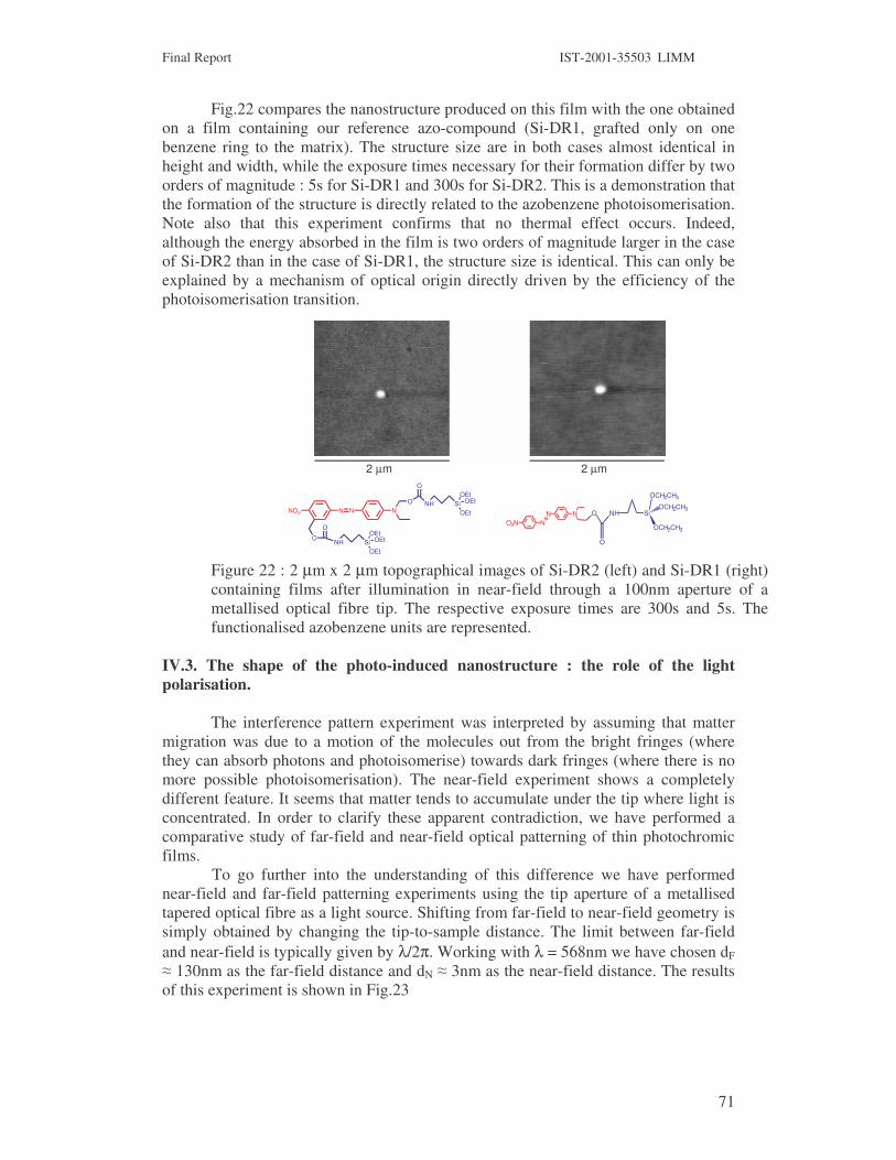
Final Report IST-2001-35503 LIMM
71
Fig.22 compares the nanostructure produced on this film with the one obtained on a film containing our reference azo-compound (Si-DR1, grafted only on one benzene ring to the matrix). The structure size are in both cases almost identical in height and width, while the exposure times necessary for their formation differ by two orders of magnitude : 5s for Si-DR1 and 300s for Si-DR2. This is a demonstration that the formation of the structure is directly related to the azobenzene photoisomerisation. Note also that this experiment confirms that no thermal effect occurs. Indeed, although the energy absorbed in the film is two orders of magnitude larger in the case of Si-DR2 than in the case of Si-DR1, the structure size is identical. This can only be explained by a mechanism of optical origin directly driven by the efficiency of the photoisomerisation transition.
2 µm
O
NH Si
OCH2CH3
OCH2CH3
OCH2CH3
NNNO2N
O
2 µm
NO2 N
O
N NO
O
NH SiOEt
OEt
OEt
NH SiOEt
OEt
OEt
O
Figure 22 : 2 µm x 2 µm topographical images of Si-DR2 (left) and Si-DR1 (right) containing films after illumination in near-field through a 100nm aperture of a metallised optical fibre tip. The respective exposure times are 300s and 5s. The functionalised azobenzene units are represented.
IV.3. The shape of the photo-induced nanostructure : the role of the light polarisation.
The interference pattern experiment was interpreted by assuming that matter migration was due to a motion of the molecules out from the bright fringes (where they can absorb photons and photoisomerise) towards dark fringes (where there is no more possible photoisomerisation). The near-field experiment shows a completely different feature. It seems that matter tends to accumulate under the tip where light is concentrated. In order to clarify these apparent contradiction, we have performed a comparative study of far-field and near-field optical patterning of thin photochromic films. To go further into the understanding of this difference we have performed near-field and far-field patterning experiments using the tip aperture of a metallised tapered optical fibre as a light source. Shifting from far-field to near-field geometry is simply obtained by changing the tip-to-sample distance. The limit between far-field and near-field is typically given by λ/2π. Working with λ = 568nm we have chosen dF � 130nm as the far-field distance and dN � 3nm as the near-field distance. The results of this experiment is shown in Fig.23

Final Report IST-2001-35503 LIMM
72
Figure 23 : 2 µm x 2 µm images of pattern inscribed on a 20 nm-thick film under far-field illumination conditions for two different direction of the injected light polarisation (indicated by red arrows), and under near-field illumination conditions.
The left image shows the topography of the surface after local illumination in far-field through the tip when the light injected into the fiber is linearly polarised. This irradiation produces a 500 nm diameter hollow surrounded by two diametrical protrusions. The material response is in fact similar to the one observed in the far-field experiments of surface relief grating printing mentioned above. The azobenzene molecules tend to move (pulling the matter) away from the illuminated area, which leaves a hollow. This migration takes place along the direction defined by the light polarisation and results in the formation of the two diametrical protrusions on both sides of the hollow corresponding to matter accumulation out of the bright spot. When the injected light polarisation is rotated by 45° (centre image), the whole pattern (the hollow surrounded by the two diametrical protrusions) is rotated by the same angle, confirming that the light polarisation defines the direction of the molecule motion. Thereafter, if the tip is brought in the near-field of the film surface, at the distance dN from the surface, the illumination produces a dot of 60nm diameter (right image). As already mentioned, in contrast with the far-field experiment performed with the same tip, photo-induced matter migration leads here to a film swelling in the area irradiated by the tip. It is still generated by the repeated trans-cis-trans isomerization cycles of the azobenzene moiety but according to an electromagnetic field distribution which must be very different. The determination of the electromagnetic near-field distribution close to a tip aperture is a difficult problem to which many theoretical works are dedicated. We have performed experiments in an other configuration which allows to evaluate qualitatively the near-field direction. This configuration is based on apertureless near-field microscopy techniques. The light nanosource is no more an optical fiber tip but a bulk metallic tip. Under external far-field illumination, light is concentrated at the tip apex which provides in near-field a local light source which spatial extension is given by the radius of curvature of the tip apex. The advantage of this configuration is that the polarisation and the angle of incidence of the exciting light with respect to the tip

Final Report IST-2001-35503 LIMM
73
axis can be chosen. Then, for a large angle of incidence (Fig.24), a p-polarised excitation induces a large field under the tip mainly oriented along the tip axis while a s-polarisation induces a weak field under the tip which is mostly parallel to the surface (i.e. perpendicular to the tip axis).
As shown from the images of Fig.24, with the apertureless technique, a nanostructure similar to the one obtained with a metallised tapered optical fibre is formed under the tip only with p-polarisation, i.e. only when the light electric field under the tip is oriented along the tip axis. This indicates that the shape of the nanodot formed in near-field is directly related to the "longitudinal" character of the field close
to the tip. This is clearly demonstrated with the apertureless techniques, but in fact, it is also the case in the aperture near-field configuration. Indeed, at the aperture of a metallised tapered optical fibre, the discontinuity between the metal coating and the glass induces a strong longitudinal field component which is by nature evanescent (i.e. which only exists very close to the tip). Because of the subwavelength size of the aperture, this component dominates the electric field distribution under the tip. One can then imagine that, under this excitation conditions, the molecules which tend to move along the field axis induces the growth of a structure under the tip perpendicularly to the film surface. IV.4. The kinetics of the photo-induced surface patterning process.
A considerable amount of work is dedicated to the study and the optimisation of the photo-induced patterning of azo-polymer films. However, as we already mentioned, the microscopic mechanism which is at the origin of the photo-induced patterning of the azo-polymer film is still not fully understood and the interpretation of many experimental data is even controversial. The most surprising is that the behaviour is completely different when illuminating the sample in far field or in near field. Indeed, most of the experiments performed in near-field show that a dot is growing under the nanometric light source. This apparent accumulation of matter in
p-polarisation s-polarisation
Figure 24 : 2 µm x 2µm images of the pattern formed on azo-hybrid film with apertureless near-field microscopy techniques under p-polarised and s-polarised excitation conditions.
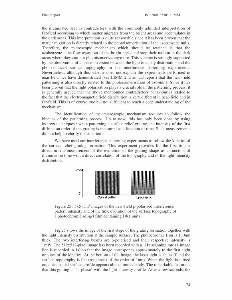
Final Report IST-2001-35503 LIMM
74
the illuminated area is contradictory with the commonly admitted interpretation of far-field according to which matter migrates from the bright areas and accumulates in the dark areas. This interpretation is quite reasonable since it has been proven that the matter migration is directly related to the photoisomerisation of the azobenzene units. Therefore, the microscopic mechanism which should be retained is that the azobenzene units flow away out of the bright areas and stop their motion in the dark areas where they can not photoisomerize anymore. This scheme is strongly supported by the observation of a phase inversion between the light intensity distribution and the photo-induced surface topography in the interference patterning experiments. Nevertheless, although this scheme does not explain the experiments performed in near-field, we have demonstrated (see LIMM 2nd annual report) that the near-field patterning is also directly related to the photoisomerisation of azo-units. Since it has been proven that the light polarisation plays a crucial role in the patterning process, it is generally argued that the above mentionned contradictory behaviour is related to the fact that the electromagnetic field distribution is very different in near-field and in far-field. This is of course true but not sufficient to reach a deep understanding of the mechanism.
The identification of the microscopic mechanism requires to follow the kinetics of the patterning process. Up to now, this has only been done by using indirect techniques : when patterning a surface relief grating, the intensity of the first diffraction order of the grating is measured as a function of time. Such measurements did not help to clarify the situation.
We have used our interference patterning experiments to follow the kinetics of the surface relief grating formation. This experiment provides for the first time a direct in-situ measurement of the evolution of the grating shape as a function of illumination time with a direct correlation of the topography and of the light intensity distribution.
Figure 25 : 5x5 �m2 images of the near-field p-polarised interference pattern intensity and of the time evolution of the surface topography of a photochromic sol-gel film containing DR1 units.
Fig.25 shows the image of the first stage of the grating formation together with the light intensity distribution at the sample surface. The photochromic film is 130nm thick. The two interfering beams are p-polarised and their respective intensity is 1mW. The 512x512-pixel image has been recorded with a 1Hz scanning rate (1 image line is recorded in 1s) so that the image corresponds approximately to the first eight minutes of the kinetics. At the bottom of the image, the laser light is shut-off and the surface topography is flat (roughness of the order of 1nm). When the light is turned on, a sinusoidal surface profile appears almost immediately. The remarkable feature is that this grating is "in-phase" with the light intensity profile. After a few seconds, the
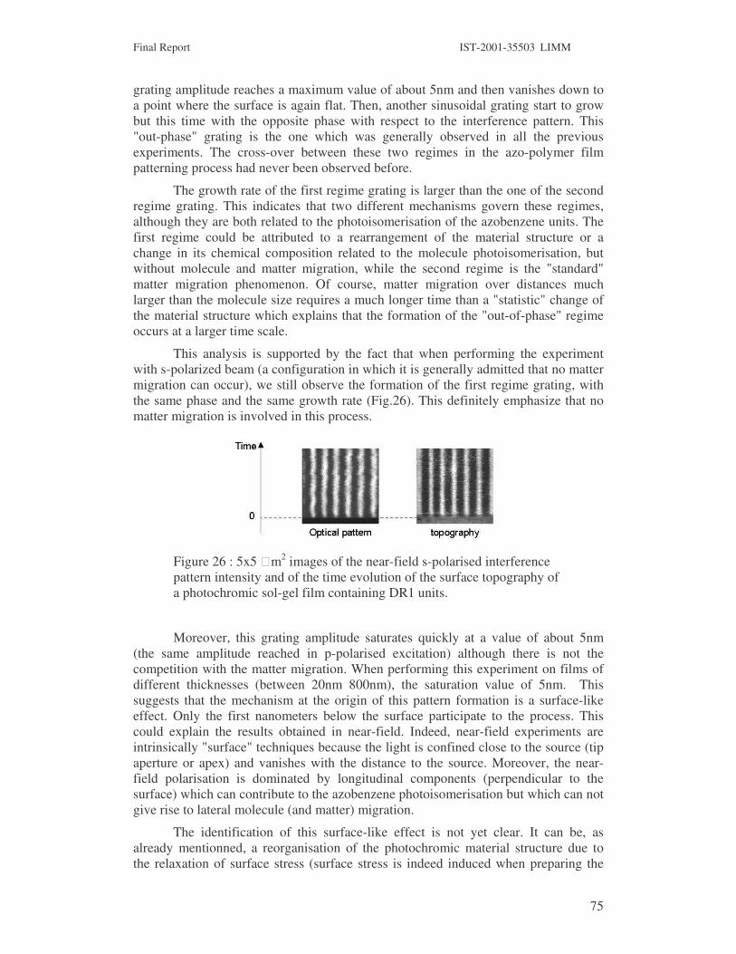
Final Report IST-2001-35503 LIMM
75
grating amplitude reaches a maximum value of about 5nm and then vanishes down to a point where the surface is again flat. Then, another sinusoidal grating start to grow but this time with the opposite phase with respect to the interference pattern. This "out-phase" grating is the one which was generally observed in all the previous experiments. The cross-over between these two regimes in the azo-polymer film patterning process had never been observed before.
The growth rate of the first regime grating is larger than the one of the second regime grating. This indicates that two different mechanisms govern these regimes, although they are both related to the photoisomerisation of the azobenzene units. The first regime could be attributed to a rearrangement of the material structure or a change in its chemical composition related to the molecule photoisomerisation, but without molecule and matter migration, while the second regime is the "standard" matter migration phenomenon. Of course, matter migration over distances much larger than the molecule size requires a much longer time than a "statistic" change of the material structure which explains that the formation of the "out-of-phase" regime occurs at a larger time scale.
This analysis is supported by the fact that when performing the experiment with s-polarized beam (a configuration in which it is generally admitted that no matter migration can occur), we still observe the formation of the first regime grating, with the same phase and the same growth rate (Fig.26). This definitely emphasize that no matter migration is involved in this process.
Figure 26 : 5x5 �m2 images of the near-field s-polarised interference pattern intensity and of the time evolution of the surface topography of a photochromic sol-gel film containing DR1 units.
Moreover, this grating amplitude saturates quickly at a value of about 5nm (the same amplitude reached in p-polarised excitation) although there is not the competition with the matter migration. When performing this experiment on films of different thicknesses (between 20nm 800nm), the saturation value of 5nm. This suggests that the mechanism at the origin of this pattern formation is a surface-like effect. Only the first nanometers below the surface participate to the process. This could explain the results obtained in near-field. Indeed, near-field experiments are intrinsically "surface" techniques because the light is confined close to the source (tip aperture or apex) and vanishes with the distance to the source. Moreover, the near-field polarisation is dominated by longitudinal components (perpendicular to the surface) which can contribute to the azobenzene photoisomerisation but which can not give rise to lateral molecule (and matter) migration.
The identification of this surface-like effect is not yet clear. It can be, as already mentionned, a reorganisation of the photochromic material structure due to the relaxation of surface stress (surface stress is indeed induced when preparing the

Final Report IST-2001-35503 LIMM
76
film by spin-coating). This stress relaxation is favoured in the illuminated area because of the mobility resulting from the photo-isomerisation. But we can not exclude that photo-chemical reactions occurring under light excitation in ambient air could induce the formation of a pattern in such a. The depth extension of such a reaction in the material could be limited by the diffusion of species (water…).
IV.5. The role of the photo-bleaching
The observation of two different pattern formation mechanisms in sol-gel films containing azobenzene units, one being mainly a surface effect in-phase with light excitation and the other being a volume effect with an opposite phase with respect to light excitaion, rules out the apparent contradiction between far-field and near-field experiments and clarify the interpretation of the patterning process. Experiments performed in controlled (oxygen free or dry) atmosphere could reinforce the interpretation that we propose for the fast-rate patterning mechanism at the origin of the pattern formation without matter migration observed in near-field experiments and in s-polarised far-field configurations.
It remains that the slow-rate out-phase matter migration phenomena is an efficient patterning process which allow to induce optically artificial structure over large area. However, in the interference patterning experiment, the amplitude of the photo-induced surface relief tends to saturate at a value of a few hundreds of nanometers even for a thick film (800nm). In fact, the patterning process is, at the end, limited by the photo-bleaching of the azobenzene units. Indeed, the light transmission T of a sol-gel film containing azobenzene molecules at a wavelength of 473nm (Fig.27) increases with exposure time and the laser spot leaves a permanently transparent area in the film. When plotting Log[Log(1/T)] as a function of time, one clearly observed two regimes : a short-time scale regime which corresponds to the settlement of the photo-stationary state between trans- and cis-isomers of the azobenzene units and a long time scale regime which is governed by the bleaching of the photochromic molecules.

Final Report IST-2001-35503 LIMM
77
Figure 27 : Variation, with exposure time, of the light transmitted T through a 50nm-thick sol-gel film, for a wavelength of 473nm. The plot of Log[Log(1/T)] clearly exhibits two regime characteristic of the shift of the photochemical equilibrium due to the molecule bleaching.
Nevertheless, the bleaching is somehow an advantage. Indeed, during their optical life time, the molecules can cross a significant distance (of the order of 1µm) driving the matter migration and then the pattern formed on the surface remains definitely stable since, when the molecules are bleached, no matter migration can occur anymore.
V. FUTURE APPLICATIONS OF PHOTO-INDUCED PATTERNING OF AZO-HYBRID FILMS.
V.1. PHOTO-CONTROLLED TRACTION OF A FLUORESCENT LABEL.
V.1.1. Strategy
One of the project objective was to use the azobenzene unit as a "truck" activated by light to control the motion and the positioning of another moiety of specific functionality which exhibits a functionality. We have decided to demonstrate this potential application by grafting to the azobenzene unit a fluorescent dye, the position and motion of which can be optically detected. Beside the potential applications, this experiment could provide quantitative information on the light-induced motion of isolated single molecules. The azobenzene derivative which seemed to be the best candidate for that purpose, with respect to organic synthesis,

Final Report IST-2001-35503 LIMM
78
was the methyl-orange (Fig.28). Unfortunately, we were not successful with this synthesis. Moreover, it was impossible to elaborate good quality (with respect to near-field techniques requirements) sol-gel films containing methyl-orange units (instead of DR1) grafted to the matrix and exhibiting photo-induced matter migration properties. We had to conclude that methyl-orange is probably not the right azobenzene derivative to use for dye-label experiment.
Figure 28 : Strategy for the synthesis of a molecular complex combining an azobenzene derivative (methyl-orange), a linker chain to silica and a fluorescent dye.
Therefore, in the last contract year, we have reoriented our strategy towards the use of Si-DR1 units, for which the sol-gel material synthesis and the conditions of controlled light-induced matter migration phenomena are well established. We have chosen as the dye an oxazine derivative which exhibits a light absorption band and a fluorescence band out of the absorption band of the DR1 azobenzene derivative (Fig.29).
Figure 29 : Oxazine dye chosen for fluorescence tracking of molecular motion. Absorption and fluorescence spectra of oxazine (red curves) with the absorption spectrum of the DR1 (blue curve).
Different processes were tried to synthesise a molecular complexe which couples this oxazine dye with Si-DR1 azo-compound (Fig.30) but, up to now, none was conclusive (see WP2).

Final Report IST-2001-35503 LIMM
79
NNNO2N
Si
O
OO
O
O C
O
matrix
hνννν
hνννν
fluorescentunit
Figure 30 : Possible scheme of a molecular complex coupling Si-DR1 with a fluorescent dye.
V.1.2. Near-field optical imaging of fluorescent thin films.
Although the synthesis of a molecular complex associating an azo-compound and a fluorescent dye failed, it is still possible in principle to follow the photo-induced mater migration in polymeric films by using a fluorescent dye dispersed in the photochromic film. Indeed, the photo-induced migration of the matter containing the dyes should result in an inhomogeneous fluorescence of the film related to the topographic surface pattern. Therefore, near-field imaging of the film fluorescence should provide the spatial distribution of the dye molecules.
However, it has not been possible to perform this measurement. Indeed, when organic molecules are not grafted to the matrix, the concentration of molecules in the film is very small : about three or four orders of magnitude less than 1 molecules per nm3, which is the concentration obtained with grafted molecules. Therefore, when using a light excitation power of a few mW (which is the typical power that can be used for such experiment without damage of the film or of the tip) and accounting for the absorption cross section and the fluorescence quantum efficiency of the dye, for the collection efficiency of the tip (less than 10-6) and for the efficiency of the optical detector, one can expect to count at best 0.1 fluorescence photon per second on a given position of the tip. In order to obtain a fluorescence image over an area 1 µm2 with a tip of 100nm-diameter aperture and a signal-to-noise ratio of about 10, one would need about three hours. These are obviously unrealistic conditions for performing reliable imaging experiment.
This task could only be reasonably achieved with functionalised dyes that could be grafted in high concentration to the polymeric matrix or with fluorescent nanoparticules having a much larger absorption cross section than molecules. The synthesis of such materials is under progress.
V.2. LARGE SCALE OPTICAL PATTERNING OF PHOTOCHROMIC FILMS.
V.2.1. Large scale optical patterning through a pre-patterned metallic mask.
In order to attain large scale patterning of photochromic films with nanometric resolution, one has to use a parallel single-shot patterning process instead of a

Final Report IST-2001-35503 LIMM
80
scanning technique. We intend to develop a process similar to those of lithography technology where the photochromic film is irradiated by light through a pre-patterned metallic mask (Fig.31). Each aperture in the metallic mask acts as a local light source. The photo-induced pattern on the film is the result of the electromagnetic field distribution that creates in near-field the ensemble of local sources.
Figure 31 : Principle of large scale optical patterning of a azo-film using a pre-patterned metallic mask in near-field configuration.
Two masks have been elaborated by Partner 2 : one is a 50nm-thick aluminium film and the other is a 50nm-thick chromium film. The metallic films have been deposited on a glass substrate by evaporation in vacuum and have been patterned by Focused Ion Beam technique. The typical pattern has a cross or star-fish shape of 10�m total size, with a pitch width of about 200nm.
We have characterised the properties of these patterns as multiple nanometric light sources for photochromic film patterning. This characterisation consists in measuring, by scanning near-field optical microscopy, the distribution of the light transmitted through the pattern. Fig.32 shows the topographic image (left image) of such a pattern obtained by shear-force microscopy and the light distribution (right image) detected simultaneously in near-field, under back illumination with a blue laser. The incident light is linearly polarised along the direction indicated by the arrow.
Figure 32 : 10x10 �m2 images of the topography (left image) and of the transmitted light distribution (right image) measured simultaneously by shear-force and near-field optical microscopy on a pre-patterned metallic mask.

Final Report IST-2001-35503 LIMM
81
It appears that the near-field light distribution significantly differs from the pattern shape itself, although one retrieves the main characteristics. This is what one expects since the metallic mask is indeed an ensemble of elementary light sources and the field in the vicinity of the surface results from the interference of the light diffracted by all these elementary sources. Therefore, it should be possible to obtain a complex photo-induced pattern on an azo-film by designing a quite simple mask Moreover, Fig.32 shows that the near-field light distribution strongly depends on the incident light polarisation. Indeed, the branches parallel to the light polarisation appears as much brighter than those perpendicular to the light polarisation. This polarisation dependence could be a powerful tool for tuning the matter migration process in azo-films.
We did not yet use these metallic masks for patterning photochromic films. For that purpose we need to develop a sample older which allows first to bring the whole mask in near-field of the photochromic film and second to position subsequently the shear-force microscope tip in coincidence with the patterned surface. This work is under progress.
V.2.2. Large scale optical patterning with interfering laser beams.
Another way to produce large scale patterning of azo-film is the interference technique. We have developed an interference patterning experiment shown in Fig.33. The beam of a diode-pumped solid state laser emitting at 473nm is separated into two beams of equal intensity. These two p-polarised beams intercept at the surface of the photochromic film, leading to the formation of interference fringes perpendicular to the plane of incidence (and perpendicular to the light polarisation). The sample is illuminated from the back side of the glass substrate so that the photochromic film faces onto the optical fiber tip of our near-field optical microscope coupled with the shear-force microscope. This geometry allows to measure in-situ, simultaneously, and with the same probe, both the light intensity distribution in near-field of the sample surface and the surface topography of the photochromic film, i.e. the photo-induced topographic pattern resulting from matter migration.
Figure 33 : Picture of the interference pattern experiment with in-situ near-field detection of the light intensity pattern and of the surface topography.
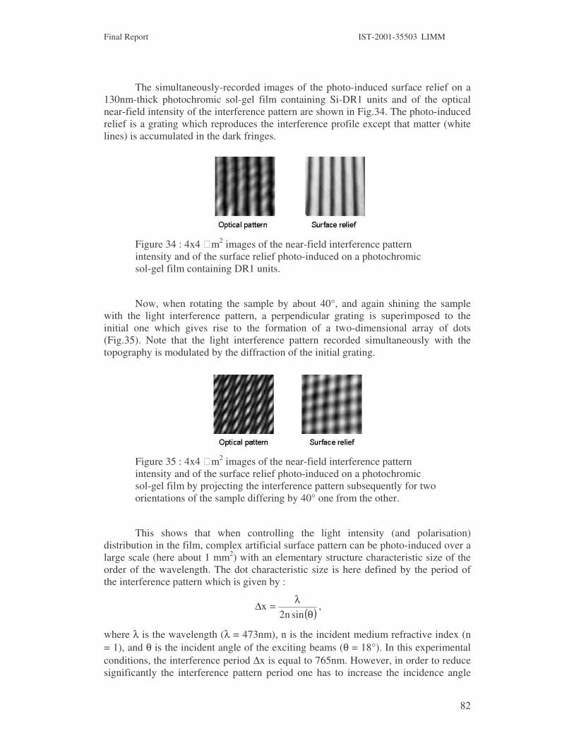
Final Report IST-2001-35503 LIMM
82
The simultaneously-recorded images of the photo-induced surface relief on a 130nm-thick photochromic sol-gel film containing Si-DR1 units and of the optical near-field intensity of the interference pattern are shown in Fig.34. The photo-induced relief is a grating which reproduces the interference profile except that matter (white lines) is accumulated in the dark fringes.
Figure 34 : 4x4 �m2 images of the near-field interference pattern intensity and of the surface relief photo-induced on a photochromic sol-gel film containing DR1 units.
Now, when rotating the sample by about 40°, and again shining the sample with the light interference pattern, a perpendicular grating is superimposed to the initial one which gives rise to the formation of a two-dimensional array of dots (Fig.35). Note that the light interference pattern recorded simultaneously with the topography is modulated by the diffraction of the initial grating.
Figure 35 : 4x4 �m2 images of the near-field interference pattern intensity and of the surface relief photo-induced on a photochromic sol-gel film by projecting the interference pattern subsequently for two orientations of the sample differing by 40° one from the other.
This shows that when controlling the light intensity (and polarisation) distribution in the film, complex artificial surface pattern can be photo-induced over a large scale (here about 1 mm2) with an elementary structure characteristic size of the order of the wavelength. The dot characteristic size is here defined by the period of the interference pattern which is given by :
( )θλ=∆
sinn2x ,
where λ is the wavelength (λ = 473nm), n is the incident medium refractive index (n = 1), and θ is the incident angle of the exciting beams (θ = 18°). In this experimental conditions, the interference period ∆x is equal to 765nm. However, in order to reduce significantly the interference pattern period one has to increase the incidence angle

Final Report IST-2001-35503 LIMM
83
and/or the refractive index of the incident medium. This is possible when performing the same experiment but in total reflection geometry (Fig.36).
Figure 36 : Principle of the optical interference patterning experiment in total reflexion geometry.
When using a total reflection glass prism of refractive index n = 1.51 (identical to the one of the sample glass substrate) and an angle of incidence in the prism of 45°, one obtain an interference pattern of period ∆x = 221nm. As shown in Fig.37, the photo-induced surface relief grating has a period 3.5 times smaller than the one obtain in the non-total reflection geometry.
Figure 37 : 4x4 �m2 topographical images of the surface relief gratings photo-induced on a photochromic sol-gel film containing DR1 units with n = 1 and � = 18° (left image) and with n = 1.51 and � = 45° (right image).
One can even expect to reach easily patterning periods smaller than 100nm, by using circularly polarised incident light and a higher incident angle.
V.3. EXTENSION OF THE PATTERNING METHOD TO OTHER MATERIALS : PHOTO-INDUCED MATTER MIGRATION IN AMORPHOUS AS2S3.
Photo-induced matter migration phenomena have been observed in amorphous As2S3. Fig.38 shows the result that we have obtained on a 100nm-thick As2S3 film deposited by spin-coating on a glass substrate. The topography of the film measured by shear-force microscopy after illumination through a non-metallised optical fiber tip exhibits a ring structure characteristic of the electromagnetic field diffracted by the non-metallised tip.

Final Report IST-2001-35503 LIMM
84
S
As
SS
As
SS
As
As
S
a
Figure 38 : a) Amorphous As2S3 network. b) As2S3 film deposited on a glass substrate. The yellow-green colour is characteristic of the amorphous As2S3 bandgap (of the order of 2.6 eV). c) Shear-force image of the As2S3 film surface after illumination in near-field through a non-metallised optical fiber tip.
The As2S3 system is very different from the photochromic materials containing azobenzene molecules since amorphous As2S3 is a homogeneous inorganic material. Nevertheless, in both systems, the origin of the photo-induced matter migration is very similar : it is due to a change in conformation of the absorbing units. In As2S3, the change in conformation corresponds to an inversion of the AsS3 tetrahedral structure (Fig.39). This phenomenon is known since many years to occur in such chalcogenide materials.
S
As
S S
S
As
S S
Figure 39 : Scheme of the configuration inversion of the As2S3 tetrahedral structure.
VI. CONCLUSION. All the tasks of WP4 have been fulfilled except the detection of the molecular motion with a fluorescent label.
We have synthesised sol-gel films containing photoactive azobenzene derivatives. These materials have been optimised for the application of surface and thin films optical patterning.
We have developed optical patterning techniques for the azo-polymeric materials based on the optical control of the azobenzene molecule motion. The available patterning scale ranges from a few �m2 to a few mm2, with a resolution between 35nm to 1µm. For high resolution patterning, near-field optical techniques are required. With far-field techniques, structures of larger characteristic size (of the order of several hundreds of nanometers) can be produced. We have studied in details the microscopic mechanisms responsible for the patterning process. These mechanisms are very different in far-field and in near-field, although they are both related to the azobenzene photoisomerisation. Indeed, in far-field, optical patterning results from the well-known photo-induced matter migration phenomenon, while, in near-field, the patterned is formed after a local change in the

Final Report IST-2001-35503 LIMM
85
material configuration close to the surface. This mechanism had never been evidenced before. This discovery is of primary importance for future developments of optical surface patterning. We have started to extend the optical patterning techniques to other materials like inorganic amorphous semiconductors which may opened new technological applications.

Final Report IST-2001-35503 LIMM
86
WP5: Photocontrolled current between electrodes across molecular wires
The aim of this WP was to assemble a molecular device that allows for controlling the
current flowing between two electrodes by an external signal as light. The device is
based on molecules incorporating AZO units, which, under light excitation, are
known to undergo isomerizations. Three fundamental requirements are need to be
fulfilled to assemble such a device. The first is that the molecules must switch when
they are organized in self assembled monolayers (SAM) anchored to a metal surface,
the second is that the molecules must switch when they are sandwiched between two
electrodes, and the third is that the two isomers must transport a different amount of
current between the electrodes.
We have used a versatile junction based on Hg for these measurements (Fig
1). The junction has been designed to allows for irradiation of the molecules when
incorporated at the interface of the junction (see below). We also assembled a second
type of junction based on conductive polymer electrodes that is suitable for
application in molecular electronics.
Fig 1. The Hg-based molecular junction and the schematized interface

Final Report IST-2001-35503 LIMM
87
We have prepared surfaces patterned with a SAM (SAM(1)) by micro-contact
printing. We have showed that (a) it is possible to assemble a different SAM made of
a different molecule (SAM(2)) on the free areas without replacing SAM(1); (b) these
surfaces have shown to be stable in our junction allowing to electrical measurements;
Fig. 2 shows an AFM image of an Au surface, where two different SAMs (COOH
and CH3 terminating) have been patterned by micro-contact printing. One can clearly
see the line pattern.
Fig. 2. AFM height profile of a surface pattern on Au (SAM(1): hexadecanethiol;
SAM(2): 15-Mercaptopentadecan carboxylic acid).
1. Surface patterned with alkanethiols of different lenght
Current measurements have been performed using the metal-SAM-Hg junction on
the surfaces patterned by alkanethiol of different length. Fig. 3 shows the I/V
characteristics of a junction based on such a patterned film. The quality of the data is
well comparable to those for conventional films, which proves that SAMs prepared by
microcontact printing are principally suitable for application in the electrical junction.
A major obstacle for the application of patterned films is the roughness of the metal
surfaces prepared by thermal evaporation. This roughness is in the size range of the
surface pattern thus hampering the concept to use the SAM with the longer molecules
as spacer between the two electrodes in the junction.
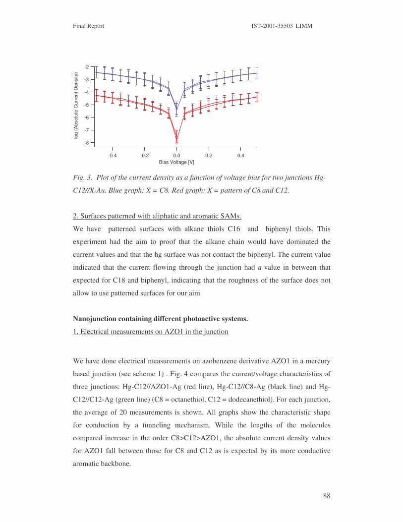
Final Report IST-2001-35503 LIMM
88
-8
-7
-6
-5
-4
-3
-2
log
(Abs
olut
e C
urre
nt D
ensi
ty)
-0.4 -0.2 0.0 0.2 0.4Bias Voltage [V]
Fig. 3. Plot of the current density as a function of voltage bias for two junctions Hg-
C12//X-Au. Blue graph: X = C8. Red graph: X = pattern of C8 and C12.
2. Surfaces patterned with aliphatic and aromatic SAMs.
We have patterned surfaces with alkane thiols C16 and biphenyl thiols. This
experiment had the aim to proof that the alkane chain would have dominated the
current values and that the hg surface was not contact the biphenyl. The current value
indicated that the current flowing through the junction had a value in between that
expected for C18 and biphenyl, indicating that the roughness of the surface does not
allow to use patterned surfaces for our aim
Nanojunction containing different photoactive systems.
1. Electrical measurements on AZO1 in the junction
We have done electrical measurements on azobenzene derivative AZO1 in a mercury
based junction (see scheme 1) . Fig. 4 compares the current/voltage characteristics of
three junctions: Hg-C12//AZO1-Ag (red line), Hg-C12//C8-Ag (black line) and Hg-
C12//C12-Ag (green line) (C8 = octanethiol, C12 = dodecanethiol). For each junction,
the average of 20 measurements is shown. All graphs show the characteristic shape
for conduction by a tunneling mechanism. While the lengths of the molecules
compared increase in the order C8>C12>AZO1, the absolute current density values
for AZO1 fall between those for C8 and C12 as is expected by its more conductive
aromatic backbone.

Final Report IST-2001-35503 LIMM
89
Scheme 1. Thiol derivatized rigid azo-systems for SAM formation and their assembly on Au surfaces.
-7
-6
-5
-4
-3
log
(Abs
olut
e C
urre
nt D
ensi
ty)
-0.4 -0.2 0.0 0.2 0.4Bias Voltage [V]
Fig. 4. Plot of the current density as a function of voltage bias for the junctions Hg-
C12//X-Ag. Black line: X = C8; green line: X = C12; red line: X = AZO1.
2. “Conductivity” of the E and Z AZO isomers.
One of the fundamental requirement to assembly a molecular device based on
AZO compounds is that the two E and Z isomers have different “conductivity”. We
measured current flowing between two electrodes through SAMs of the E and Z form
by using as test bed a Hg based junctions (Fig 1).
The first junction incorporated SAM formed by the E form of AZO1. The second
junction incorporate SAMs formed by the Z form of AZO1. Comparing the current
density at 0.5 volts, we found that the current flowing through the Z form is
N N
S
2
AZO1 AZO2
metal
NN
S
E-form (stable)
20° NN
S
NN
S
NN
S
N N
SH
a) b)

Final Report IST-2001-35503 LIMM
90
around 10-5 A/cm2) two order of magnitude higher than the current flowing
trough the E form (currents of about 10-3A/cm2).
2. The photoswitching junction
The second fundamental requirement to obtain a switching molecular device is
that the molecule must be able to switch when they are sandwiched between two
electrodes. For this purpose, we have assembled a new junction that allows for
irradiation of the AZO SAMs inside the assembled junction. If the
photoisomerization takes place, then on the basis of the different “conductivity”
reported for the E and Z forms, we expect the current to change under irradiation.
a. The design of the junction
To perform the electrical measurements under irradiation, we have used the junction
that has been assembled during the first year of the project (Fig. 5). The junction
allows for irradiation of the SAMs through an ultratin layer of gold that is transparent
to light. By flipping the mirror the contact area can be recorded on a video camera.
S A M
E le c tro m e te r
V id e o c a m e ra
M ic ro m a n ip u la to r
M ic ro m a n ip u la to r
G o ldS u p p o r t
H g E le c tro d e
C o u n te r e le c tro d e (g o ld tip )
S w itc h a b le m irro r
H g S y r in g e
L O T O rie lS p e c tra lu m in a to r
O p tic a l f ib e r

Final Report IST-2001-35503 LIMM
91
Contact area
MirrorObjective
Camera
Contact area
MirrorObjective
Camera
Optical fiber
Hg Syringe CounterElectrode
Fig 5. Schematic representation and picture of the junction. The junction allows for irradiation of photoactive SAMs when assembled on a metal surfaces and sandwiched between the two metal electrodes.
b. Assembling of the molecular junction
The junction is assembled according to the following steps:
i) Deposition of ultrathin metal surfaces on mica: films of different metas (Au, Ag,
Pt) hase been deposited , ii) Preparation of the SAMs of AZO1 and AZO2 according
the a adjusted precedure, iii) assembly of the junction bringing the Hg electrode in
contact with the SAMs in an insulating solution of hexadecane.
c. Electrical measurements
By applying a constant potential across the junction, we have recorded the current
flowing through the junction under irradiation of the SAM at opportune wavelength
(370 and 450 nm) (Lot Oriel Spectraluminator).
The results for the junction 1 (incorporating AZO1) are shown in Fig 6.

Final Report IST-2001-35503 LIMM
92
-0,4 -0,2 0,0 0,2 0,41E-7
1E-6
1E-5
1E-4
1E-3
0,01
Cur
rent
Den
sity
/ A
Voltage / V
AZO1 Z-form AZO1 E-form
Fig. 6 I-V curves obtained under irradiation of junction incorporating AZO1, at 370 and 450 nm.
The results show that the current increases and decreases of two orders of magnitude
and reversibly under irradiation. We attribute this change in current to the presence of
the different isomers E and Z in the SAM sandwiched between the two electrodes.
The results show that the current increases and decreases of two orders of
magnitude and reversibly under irradiation . We attribute this change in current
to the reversible photoconversion of the different isomers E and Z in the SAM
sandwiched between the two electrodes.
d. Testing artifacts
To demonstrate that a change in current taking place under irradiation are related to
the E-Z isomerization and not to artifacts, we have performed the following tests:
- To show that the 370 nm and of 450 nm light is not causing a change in the metal
film or damaging the SAMs, we have performed measurements of current density in
junction incorporating photo-inactive molecules as alkane thiols under irradiation
with the same wavelengths. No changes in current has been detected under irradiation.
- The junction cannot undergo shortages during the measurements and under
irradiation. The AZO1 and AZO2 SAMs must be well ordered and packed in order to
provide stability of the junction during the measurements. We have characterized the

Final Report IST-2001-35503 LIMM
93
packing of the SAMs bay electrochemical measurements using K3Fe(CN)6 as redox
active site to penetrate the SAMs defects.
The results of cyclovoltammetric measurements on SAM AZO2 are reported in Fig.
7. Measuremenst on AZO1 SAM are in progress. The results of Fig 7 show that the
AZO2 SAM is permeable to redox sites and is not well packed.
Au electrode Azo thiol 11-03-05
-0.200 0.050 0.300 0.550 0.800-5-0.800x10
-5-0.550x10
-5-0.300x10
-5-0.050x10
-50.200x10
-50.450x10
E / V
i / A
Fig. 7 CV voltammogram of K3Fe(CN)6 on bare gold (blue line) and on SAMAzo2 -coated electrode (red line) (KCl 1M, 50 mV/s)
At the present state, two main problems need to be faced:
- Reproducibility of the photogated device. Only 20 % of the devices have shown an
efficient switching in current. We believe that by reducing the roughness of the metal
surfaces, and increasing the quality of the SAMs by annealing procedure will increase
the reproducibility of the device.
- The mechanism of the change in current. While the increase of current for the Z
respect to the E form can be explained by a shorter tunneling patway: in this case the
AZO E form is expected to isomerizes to the extended E form by displacinh the Hg
liquid surface of 5 Å. This hypothesis need further confirmation since: it is surprising
that the Z form can extend to the E form under the Hg contact. It is possible that the
SAMs on the Hg surface create a space available for the formation of the E form.
Prototype of a photogated device.
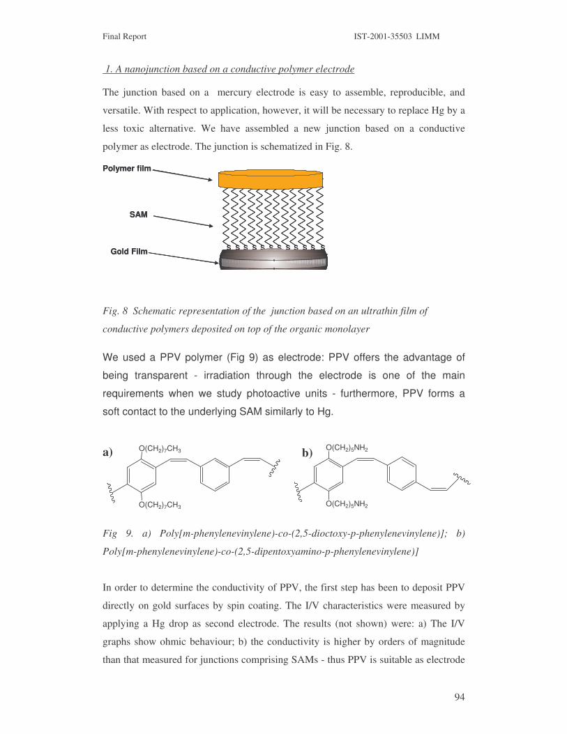
Final Report IST-2001-35503 LIMM
94
1. A nanojunction based on a conductive polymer electrode
The junction based on a mercury electrode is easy to assemble, reproducible, and
versatile. With respect to application, however, it will be necessary to replace Hg by a
less toxic alternative. We have assembled a new junction based on a conductive
polymer as electrode. The junction is schematized in Fig. 8.
s ss s s s s s s s s s
Polymer film
Gold Film
SAM
s ss s s s s s s s s s
Polymer film
Gold Film
SAM
Fig. 8 Schematic representation of the junction based on an ultrathin film of
conductive polymers deposited on top of the organic monolayer
We used a PPV polymer (Fig 9) as electrode: PPV offers the advantage of
being transparent - irradiation through the electrode is one of the main
requirements when we study photoactive units - furthermore, PPV forms a
soft contact to the underlying SAM similarly to Hg.
O(CH2)5NH2
O(CH2)5NH2
O(CH2)7CH3
O(CH2)7CH3a) b)
Fig 9. a) Poly[m-phenylenevinylene)-co-(2,5-dioctoxy-p-phenylenevinylene)]; b)
Poly[m-phenylenevinylene)-co-(2,5-dipentoxyamino-p-phenylenevinylene)]
In order to determine the conductivity of PPV, the first step has been to deposit PPV
directly on gold surfaces by spin coating. The I/V characteristics were measured by
applying a Hg drop as second electrode. The results (not shown) were: a) The I/V
graphs show ohmic behaviour; b) the conductivity is higher by orders of magnitude
than that measured for junctions comprising SAMs - thus PPV is suitable as electrode

Final Report IST-2001-35503 LIMM
95
material for our junctions; and c) the valued are scattered due to inhomogenity of the
PPV films due to poor adherence onto gold.
The prototype junction that we have fabricated using PPV is of the type Au-
SAM//PPV. The PPV is deposited on the SAM-covered gold surface by spin-coating.
For our test measurements, the polymer is contacted with the electric circuit by a drop
of Hg.
We have measured Au-SAM//PPV junctions with SAMs of C8, C10, C12, C14, and
C16 alkane thiols (Fig 10). The I-V curves exhibit i) an exponential behavior,
characteristic of a tunneling process, ii) a symmetric shape for positive and negative
bias, iii) dependence of the current intensity for a given voltage bias (for example at
0.5 V) that depends on the length of the alkyl chain forming the SAMs.
-8
-6
-4
-2
log
(Abs
olut
e C
urre
nt D
ensi
ty)
-0.4 -0.2 0.0 0.2 0.4Bias Voltage [V]
C10C12
C16C14
C8
Fi.g 10. I-V curves the junctions Hg-SAM//PPV for SAMs of different alkyl thiols CX.
The electron transfer rate is expected to follow the relationship I=Io e -βd, where d is
the length of the molecule and β is the “correlation factor”. Other authors and we have
demonstrated that such a factor β is equal to 1 for molecules formed by aliphatic
chains, while is equal to 0.5 for oligophenylene chains. On this basis we have used
aliphatic thiols of different length to form various SAMs on the Au surfaces.
From the relationship I=Io e -βd a � = 0,96 ± 0,07 A-1value is calculated. These data
are in excellent agreement with the values reported in literature and indicate that
sucha junction is reliable to be a prototype to study electron transfer processes
through molecules.
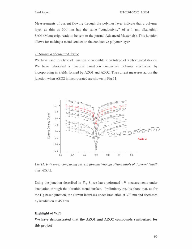
Final Report IST-2001-35503 LIMM
96
Measurements of current flowing through the polymer layer indicate that a polymer
layer as thin as 300 nm has the same “conductivity” of a 1 nm alkanethiol
SAM.(Manuscript ready to be sent to the journal Advanced Masterials). This junction
allows for making a metal contact on the conductive polymer layer.
2. Toward a photogated device
We have used this type of junction to assemble a prototype of a photogated device.
We have fabricated a junction based on conductive polymer electrodes, by
incorporating in SAMs formed by AZO1 and AZO2. The current measures across the
junction when AZO2 in incorporated are shown in Fig 11.
Fig 11. I-V curves comparing current flowing trhough alkane thiols of different length
and AZO 2.
Using the junction described in Fig 8, we have peformed i-V measurements under
irradiation through the ultrathin metal surface. Preliminary results show that, as for
the Hg based junction, the current increases under irradiation at 370 nm and decreases
by irradiation at 450 nm.
Highlight of WP5
We have demonstrated that the AZO1 and AZO2 compounds synthesized for
this project
-0,6 -0,4 -0,2 0,0 0,2 0,4 0,6
1E-9
1E-8
1E-7
1E-6
1E-5
1E-4
1E-3
0,01
Cur
rent
Den
sity
(A/c
m2 )
NN S
SN
N
AZO 2

Final Report IST-2001-35503 LIMM
97
1) exhibit reversible photoisomerization when organized on metal surfaces
and inside a metal-SAM-Hg junction and irradiated by 370 and 450 nm.
As a consequence of this conversion, the current flowing between the
electrodes through the E and Z forms change of two orders of magnitude
under irradiation. We show that the changes in current are reversible for
a number of irradiation cycles.
2) Preliminary results indicate that the same switching take place in a new
junction based on conductive polymers electrodes. This new junction
represent a prototype that can be use for future application in molecular
electronic devices.
3) Nanopatterning the metal surfaces with different SAMs does not supply a
valuable strategy to fabricate this type of devices.

Final Report IST-2001-35503 LIMM
98
WP 6 : Light-controlled single molecule motion on surface
We have achieved deposition of thin films and submonolayers of different substances
onto a wide range of substrates.
- Thin films were prepared for all azobenzene derivatives available in a sufficient
quantity.
- Submonolayers were prepared by different techniques (dipping, spin coating,...) on
different substrates (to tune the molecule/substrate interaction) and visualized by
AFM in air or in toluene (also the environment influences the molecule/substrate
interaction). The size of the Frechet type dendrimers NitroAzo2 and 3 was below the
resolution limit of our AFM. Very thin polymer (PMMA-DR1) films are dewetting.
Apart from these two extremes in size, all the other substances could be visualized by
AFM either as single molecules or small aggregates.
Samples exibiting isolated single azobenzene derivatives were obtained and could be
visualized by AFM (see fig. below)
Figure: AFM image of a sample prepared by dipping SiO2 in a solution of G4
(concentration 3mg/l in dichloromethane) for 10 sec. The bright spots represent G4
molecules.

Final Report IST-2001-35503 LIMM
99
Substances studied: GX, GX-MO (X=2,3,4, 5), NitroAzo2 and 3, gold nanoparticles
functionalized with methyl orange derivatives MO-S,
Substrates studied: Si-H, SiO2, glass, mica, mica-EDA (NH2 terminated), mica-DMP
(phenyl terminated), Au, Alkylthiol self-assembled on gold, MO-azo disulfide
derivatives self assembled on gold.
Nearly all possible combinations have been tested, and positive results have been
obtained :
-on glass (transparent and flat) for thin films
-on (functionalized) mica (less transparent but flatter than glass) for nanometer-sized
objects such as G4MO.
Light patterning of thin films and of submonolayers - Results
For thin films, Light Induced Mass Motion (LIMM) is always observed when
the samples are exposed to an interference pattern.
As an example, the figure below shows an AFM image of a thin layer of azobenzene
derived dendrimers after irradiation with a 473 nm light interference pattern
Legend: Thin film of G2-MO/glass light patterned and visualized with AFM.
From these experiments we can make three important observations:

Final Report IST-2001-35503 LIMM
100
-the amplitude of the surface modulation is never large enough to completely deplete
the layer down to the substrate. If we start with an initial thickness h0, after
irradiation, the surface profile will ondulate (at maximum) between h0-h0/2 and
h0+h0/2. This fact can be explained by our theoretical model (see below).
- patterning occurs for all types of molecules (polymer, spherical dendrimer,...). This
rules out an explanation for the surface ondulations by anisotropy of PMMA-DR1.
-Patterning also occurs for different densities of azo-functions. For instance when
comparing the NitroAzo2 with NitroAzo3 (see Annex), both contain one azobenzene-
function per molecule while, for the latter, the „cargo fret“ is roughly multiplied by a
factor of two.
For isolated molecules, however, despite our efforts, we never observed Light
Induced Single Molecule Movement.
Under all conditions which were applied, no lateral displacement of single molecules
could be observed with AFM.

Final Report IST-2001-35503 LIMM
101
Legend: Sequence (from left to right and from top to bottom) of AFM images (lateral
dimension1.75 micron) while the sample (G5MO/Mica) is irradiated (473nm
interference pattern) using the combined Optical/Atomic Force Microscope (see D16).
No modification of the position of the G5MO molecules (except the thermal drift) can
be observed during more than 1 hour.
Light patterning of thin films - Model
We have shown in the yearly reports that the amplitude of the surface modulation
grows with the irradiation dose and saturates to a value below the initial thickness of
the film (see figure below).

Final Report IST-2001-35503 LIMM
102
Legend: Left: AFM image of a thin film of light patterned PMMA-DR1.
Right: Growth of the amplitude of the surface modulation with time.
This behaviour can be explained by a model we have developed. Photons absorbed by
the azo-functions activate cis-trans isomerisation. This isomerisation leads to a lateral
movement through a friction mechanism. The molecule is thus laterally shifted by a
distance l. The movement is directed (only the molecules with the right orientation
can absorb polarized light), but not oriented. The molecular entity moves randomly
in 1 dimension. Thus, after N jumps the molecule has moved l x �N in one direction.
Patterning occurs because of the gradient of light intensity/polarisation.
0 200 400 600 800 1000 1200-2
0
2
4
6
8
10
12
14
16
18
20
deformation amplitude vs time
defo
rmat
ion
ampl
itude
(a.
u.)
time (a.u.)
azobenzenes are: - less likely to be activated
BUT - more numerous - bleached less quickly
azobenzenes are: - more likely to be activated
BUT - less numerous - bleached more quickly Equilibrium

Final Report IST-2001-35503 LIMM
103
We will now discuss the consequences that can be derived from this model for single
molecule motion.
In the framework of this quantitative model it is possible to derive the lateral stepsize
l. We obtain l ~ 1 nm (see 2nd year report).
This implies that an isolated molecule has to jump an average of N ~104 times to
perform a lateral movement of 100nm.
For the typical power density we use (1,5mW/mm2 ), this corresponds to 10000
seconds.
However, as shown above, no movement was observed within 1 hour even with
power densities up to 15mW/mm2 .
One possible explanation is that „our“ mechanism requires that a molecule „pushes“
against something. In thin films, azomolecules have neighbours whereas, isolated on a
surface, they can only push the surface... This mechanism, if possible, is expected to
be less efficient. But it seems difficult to prove this experimentally.
However, there is also another explanation supported by the experiments: The
experiments show that photobleaching must be taken into account.
To give an idea of the order of magnitude, for a 100 nm thick film, with a power
density of 1mW/mm2, the samples (initialy absorbing 50% of the light) become
transparent within one hour. This means that all the absorbing azobenzene molecules
have been bleached. Extrapolated to a single molecule at the surface, this molecule
will have performed an average of N ~2500 isomerisation cycles before being
bleached. In terms of lateral displacement, this corresponds to l x �N ~ 50 nm only,
which is in the range of the resolution of an AFM.
During the LIMM project several experimental setup have been developed in order to
visualize the movements of a single molecule. A short overview of the experimental
systems is given below.
Prototype(s) of combined Optical/Atomic Force Microscopes
We have developed a specific setup for the LIMM project, combining an inverted
optical microscope and an AFM. This setup allows for irradiation of the sample
through its transparent substrate, during AFM imaging of the sample. We have
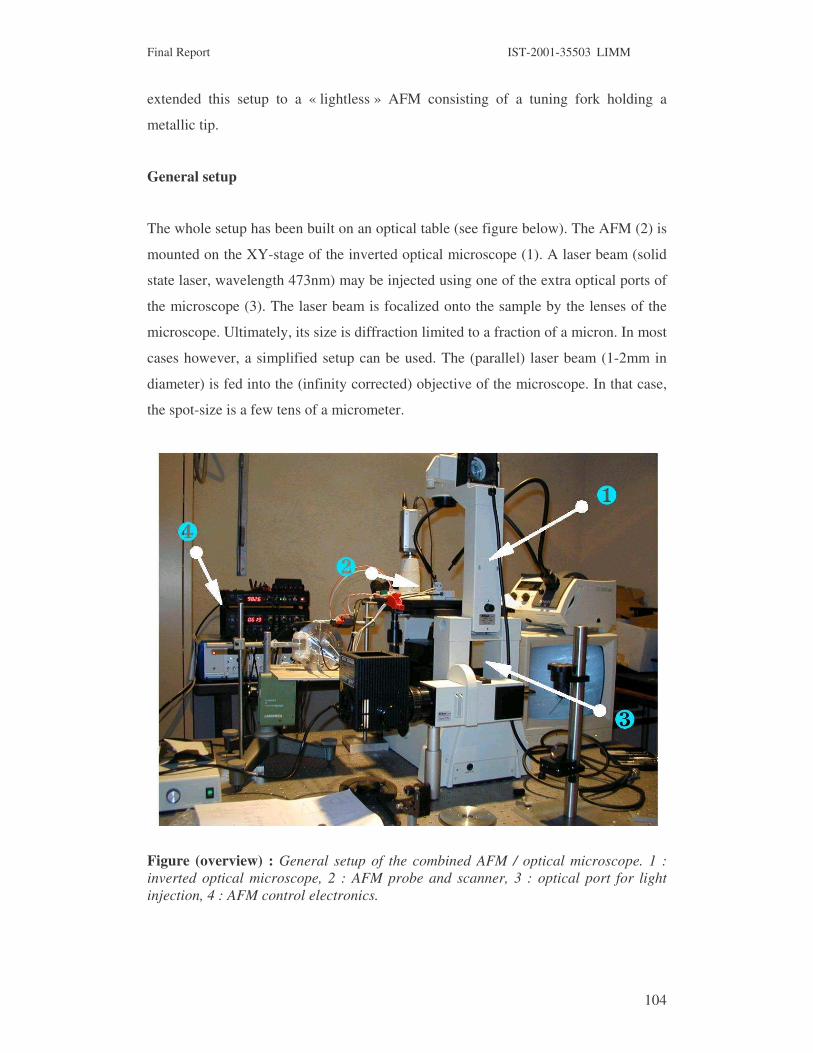
Final Report IST-2001-35503 LIMM
104
extended this setup to a « lightless » AFM consisting of a tuning fork holding a
metallic tip.
General setup
The whole setup has been built on an optical table (see figure below). The AFM (2) is
mounted on the XY-stage of the inverted optical microscope (1). A laser beam (solid
state laser, wavelength 473nm) may be injected using one of the extra optical ports of
the microscope (3). The laser beam is focalized onto the sample by the lenses of the
microscope. Ultimately, its size is diffraction limited to a fraction of a micron. In most
cases however, a simplified setup can be used. The (parallel) laser beam (1-2mm in
diameter) is fed into the (infinity corrected) objective of the microscope. In that case,
the spot-size is a few tens of a micrometer.
Figure (overview) : General setup of the combined AFM / optical microscope. 1 : inverted optical microscope, 2 : AFM probe and scanner, 3 : optical port for light injection, 4 : AFM control electronics.

Final Report IST-2001-35503 LIMM
105
Using a tilting mirror, we can move the laser spot in the whole field of view of the
optical microscope.
Combination with a classical stand-alone AFM
In this setup, a stand alone AFM is mounted on the xy-stage of the optical
microscope. The irradiation is performed through the back side of the transparent
sample.
Figure (stand-alone version) : The stand-alone AFM is mounted on the xy-stage of
the optical microscope (left). The sample, PMMA-DR1 spin coated onto glass,
appears orange while blue diffusion from the 473nm laser by theAFM tip is clearly
visible.
During AFM imaging, it is possible to monitor the relative positions of the light spot
and of the AFM probe. This is shown below, where we have performed a
displacement of an AFM probe with respect to the position of a light spot, and
controlled these positions with the optical microscope.

Final Report IST-2001-35503 LIMM
106
Figure (field of view) : B&W images of an AFM probe (the middle tip in this example) through the optical microscope while irradiating a sample with the 473nm. On the left picture, the AFM probe is at the same position than the light spot. On the right picture, the AFM probe has been moved 100 microns left. (the width of the AFM cantilever is 30 microns.) In this setup, the maximum AFM imaging area can be as large as 60x60
micron2. Compared to the damped stand-alone AFM, some additional noise (probably
due to mechanical vibrations of the xy-stage) has been observed. If necessary, this
could be improved by damping the whole system and by protecting it from acoustical
noise.
Combination with a prototype « lightless » AFM
In most AFM, the probe motion is measured with a (red) light beam deflexion
technique. For studying some photoactive systems, this could be a major drawback.
We have thus decided to develop a « lightless » AFM, where the movements of the
probes are measured electrically. One way to achieve such a goal is to use tuning
forks which oscillate around 32kHz.
The tip itself (a chemically etched metallic wire as for atomic resolution STM) is
glued at the extremity of one of the prongs of the fork (see figure below). The probe
(tip glued to the quartz tuning fork) is an electromechanical system. It can be excited
electrically (fr~32kHz) and the amplitude of the ac-current is related to the (tapping)
mechanical amplitude. Typical quality factors (Q) of our probes are in the range of
several thousands (Q ~ 6000 is typical). However the higher Q, the longer the time
response (here ~ 200ms). Although it is possible to operate our lightless microscope
in the usual mode (constant excitation frequency and amplitude), this results in
extremely low acquisition rates.
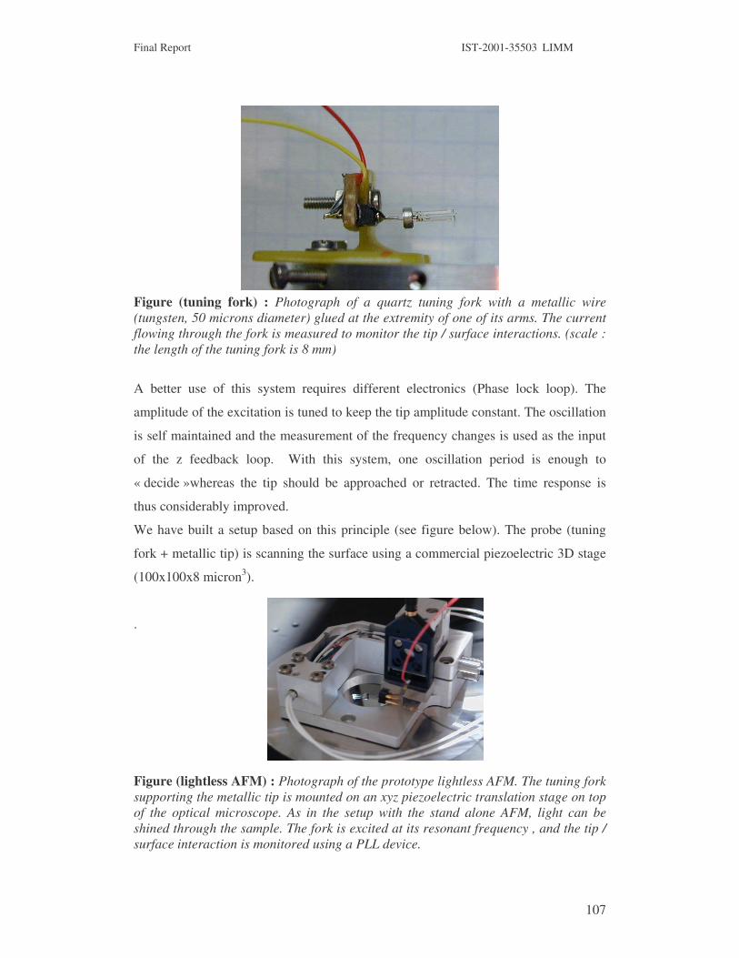
Final Report IST-2001-35503 LIMM
107
Figure (tuning fork) : Photograph of a quartz tuning fork with a metallic wire (tungsten, 50 microns diameter) glued at the extremity of one of its arms. The current flowing through the fork is measured to monitor the tip / surface interactions. (scale : the length of the tuning fork is 8 mm)
A better use of this system requires different electronics (Phase lock loop). The
amplitude of the excitation is tuned to keep the tip amplitude constant. The oscillation
is self maintained and the measurement of the frequency changes is used as the input
of the z feedback loop. With this system, one oscillation period is enough to
« decide »whereas the tip should be approached or retracted. The time response is
thus considerably improved.
We have built a setup based on this principle (see figure below). The probe (tuning
fork + metallic tip) is scanning the surface using a commercial piezoelectric 3D stage
(100x100x8 micron3).
.
Figure (lightless AFM) : Photograph of the prototype lightless AFM. The tuning fork supporting the metallic tip is mounted on an xyz piezoelectric translation stage on top of the optical microscope. As in the setup with the stand alone AFM, light can be shined through the sample. The fork is excited at its resonant frequency , and the tip / surface interaction is monitored using a PLL device.

Final Report IST-2001-35503 LIMM
108
Figure (calibration grating) : Imaging of a calibration grating with the lightless prototype AFM. Image size : 10x10 micron2, height of the grating : 10 nm.

Final Report IST-2001-35503 LIMM
109
WP 7 : Light-induced positioning and self-assembly of molecules between electrodes This WP unfortunately we were not able to achieve this WP within the length of the
project. As mentioned several times LIMM is a very risky and highly challenging
project which has brought high quality research and a full understanding of several
important processes. The difficulty encountered in the move of single molecules on
surfaces and the laborious synthesis which would eventually encountered are the main
reasons for the failing of this WP.

Final Report IST-2001-35503 LIMM
110
WP8-9-10 The LIMM project was a challenging and very ambitious proposal with a high factor of risk. We have enjoyed to work together very much and I believe that we have done a wonderful job also proving that scientist with different background and expertise can work together for a common goal. The great friendly and cooperative atmosphere of the consortium made the running of the project and the work of the coordinator very pleasant. We have surely contributed with our research and development of the LIMM to the knowledge related to the chemical and physical behavior of photoresponsive materials which can induce a molecular movement or switch a specific property. The dissemination of the results has already started with several communication at important international meetings as well as with high ranked publications in press or submitted (about 6). The consortium is still working together in order to finish the pending experiments and to complete the manuscripts (about 8). All the meetings have been held timely and the evaluations were very positive and we followed very carefully the suggestions of the evaluators each year. We finally wish to thank the EU for this great opportunity and for their support.

Final Report IST-2001-35503 LIMM
111
1st year 2nd year 1
2
3
4
5
6
Tot
WP1 : Synthesis of functional azobenzene derivatives
16 (4)
42 (13)
58
WP2 : Photophysical characterization of functional azobenzene
24 (8)
4 (1)
28
WP3 : Molecular movement in solution and sol-gel
14 (2) 8
(1) 24 (2) 46
WP4 : Photo-controlled vectorial movement for nano- scale patterning of thin films
4 (2) 48
(0) 52
WP 5 : Photocontrolled current between electrodes across molecular wires
2 (1)
60 (4)
62
WP 6 : Light-controlled single molecule motion on surface
40 (33)
14 (0) 54
WP 7 : Light-induced positioning and self-assembly of molecules between electrodes
38 (24)
38
WP 8 : Project management 6 (6)
6
WP9: Dissemination and use plan
2 (2) 2
WP10: Assessment and evaluation 0
TOTAL MAN MONTHS 62 84 50 62 64 24 346 meetings
The numbers in parenthesis indicates the man-months of permanent staff involved in the project
1st
����
���� ����
����
Top Related