


Languages
Pages
Legal


1
LTC1408
1408fa
6 Channel, 14-Bit, 600kspsSimultaneous Sampling ADC
with Shutdown
The LTC®1408 is a 14-bit, 600ksps ADC with six simulta-neously sampled differential inputs. The device drawsonly 5mA from a single 3V supply, and comes in a tiny 32pin (5mm × 5mm) QFN package. A SLEEP shutdownfeature lowers power consumption to 6µW. The combina-tion of low power and tiny package makes the LTC1408suitable for portable applications.
The LTC1408 contains six separate differential inputs thatare sampled simultaneously on the rising edge of theCONV signal. These six sampled inputs are thenconverted at a rate of 100ksps per channel.
The 90dB common mode rejection allows users toeliminate ground loops and common mode noise bymeasuring signals differentially from the source.
The device converts 0V to 2.5V unipolar inputs differen-tially, or ±1.25V bipolar inputs also differentially,depending on the state of the BIP pin. Any analog inputmay swing rail-to-rail as long as the differential inputrange is maintained.
The conversion sequence can be abbreviated to convertfewer than six channels, depending on the logic state ofthe SEL2, SEL1 and SEL0 inputs.
The serial interface sends out the six conversion results in96 clocks for compatibility with standard serial interfaces.
600ksps ADC with 6 Simultaneously SampledDifferential Inputs
100ksps Throughput per Channel 76dB SINAD Low Power Dissipation: 15mW 3V Single Supply Operation 2.5V Internal Bandgap Reference, Can be Overdriven
with External Reference 3-Wire Serial Interface Internal Conversion Triggered by CONV SLEEP (6µW) Shutdown Mode NAP (3.3mW) Shutdown Mode 0V to 2.5V Unipolar, or ±1.25V Bipolar Differential
Input Range 90dB Common Mode Rejection Tiny 32-Pin (5mm ××××× 5mm) QFN Package
Multiphase Power Measurement Multiphase Motor Control Data Acquisition Systems Uninterruptable Power Supplies
APPLICATIO SU
FEATURES DESCRIPTIO
U
BLOCK DIAGRA
W
, LT, LTC and LTM are registered trademarks of Linear Technology Corporation. All other trademarks are the property of their respective owners. Protected by U.S. Patents including 6084440, 6522187.
– +
45 2524
– +
7 691213
1619 8
CH0– CH0+CH1– CH1+
1011
– +
1415
CH2– CH2+CH3– CH3+
–
+
1718
– +
2021
S AND H S AND H S AND H S AND H S AND H
CH4– CH4+CH5– CH5+
MUX
VREF
10µF
BIP SEL2 SEL1 SEL0
GND
2.5VREFERENCE
600ksps14-BIT ADC
14-BIT LATCH 514-BIT LATCH 414-BIT LATCH 314-BIT LATCH 214-BIT LATCH 114-BIT LATCH 0
10µF 3V
VCC VDD
2629232233 27 28
2
1SD0
0.1µF
3OVDD3V
32 SCK
31 DGND
OGND
30 CONV
THREE-STATESERIALOUTPUT
PORT
TIMINGLOGIC
1408 TA01
– +
S AND H

2
LTC1408
1408fa
A
U
G
W
A
W
U
W
ARBSOLUTE XI TI S(Notes 1, 2)Supply Voltage (VDD, VCC, OVDD) .............................. 4VAnalog Input Voltage
(Note 3) ................................... – 0.3V to (VDD + 0.3V)Digital Input Voltage .................... – 0.3V to (VDD + 0.3V)Digital Output Voltage .................. – 0.3V to (VDD + 0.3V)Power Dissipation .............................................. 100mWOperation Temperature Range
LTC1408C ............................................... 0°C to 70°CLTC1408I ............................................ –40°C to 85°C
Storage Temperature Range ................. –65°C to 125°C
The denotes the specifications which apply over the full operatingtemperature range, otherwise specifications are at TA = 25°C. With internal reference, VDD = 3V, VDD = VCC = 3V.
PARAMETER CONDITIONS MIN TYP MAX UNITS
Resolution (No Missing Codes) 14 Bits
Integral Linearity Error (Note 5) –3 ±0.5 3 LSB
Offset Error (Note 4) –4.5 ±1 4.5 mV
Offset Match from CH0 to CH5 –3 ±0.5 3 mV
Range Error (Note 4) –12 ±2 12 mV
Range Match from CH0 to CH5 –5 ±1 5 mV
Range Tempco Internal Reference (Note 4) ±15 ppm/°CExternal Reference ±1 ppm/°C
The denotes the specifications which apply over the full operating temperature range,otherwise specifications are at TA = 25°C. With internal reference, VDD = 3V, VDD = VCC = 3V.
SYMBOL PARAMETER CONDITIONS MIN TYP MAX UNITS
VIN Analog Differential Input Range (Notes 3, 8, 9) 2.7V ≤ VDD ≤ 3.3V 0 to 2.5 V
VCM Analog Common Mode + Differential 0 to VDD VInput Range (Note 8)
IIN Analog Input Leakage Current 1 µA
CIN Analog Input Capacitance 13 pF
tACQ Sample-and-Hold Acquisition Time (Note 6) 39 ns
tAP Sample-and-Hold Aperture Delay Time 1 ns
tJITTER Sample-and-Hold Aperture Delay Time Jitter 0.3 ps
tSK Channel to Channel Aperture Skew 200 ps
CMRR Analog Input Common Mode Rejection Ratio fIN = 100kHz, VIN = 0V to 3V –83 dBfIN = 10MHz, VIN = 0V to 3V –67 dB
CO VERTER CHARACTERISTICS
U
A ALOG I PUT
U U
WU U
PACKAGE/ORDER I FOR ATIOORDER PART
NUMBER
QFN PART MARKING
TJMAX = 125°C, θJA = 34°C/ WEXPOSED PIN IS GND (PAD 33)MUST BE SOLDERED TO PCB
Consult LTC Marketing for parts specified with wider operating temperature ranges.
16 15 14 13 12 11 10 9
25 26 27 28
TOP VIEW
QFN PACKAGE32-PIN (5mm × 5mm) PLASTIC QFN
29 30 31 32
1
2
3
4
5
6
7
8
24
23
22
21
20
19
18
17CH4+
CH4–
GND
CH5+
CH5–
GND
VREF
VCC
CH1–
CH1+
GND
CH0–
CH0+
OVDD
OGND
SDO
GND
CH3–
CH3+
GND
GND
CH2–
CH2+
GND
V DD
SEL2
SEL1
SEL0 BIP
CONV
DGND SC
K
33
LTC1408CUHLTC1408IUH
1408
Order Options Tape and Reel: Add #TRLead Free: Add #PBF Lead Free Tape and Reel: Add #TRPBFLead Free Part Marking: http://www.linear.com/leadfree/

3
LTC1408
1408fa
I TER AL REFERE CE CHARACTERISTICSU U U
The denotes the specifications which apply over the full operating temperature range,otherwise specifications are at TA = 25°C. With internal reference, VDD = 3V, VDD = VCC = 3V.
SYMBOL PARAMETER CONDITIONS MIN TYP MAX UNITS
SINAD Signal-to-Noise Plus 100kHz Input Signal 73 76 dBDistortion Ratio 300kHz Input Signal 76 dB
100kHz Input Signal, External VREF = 3.3V, VDD ≥ 3.3V 79 dB300kHz Input Signal, External VREF = 3.3V, VDD ≥ 3.3V 79 dB
THD Total Harmonic 100kHz First 5 Harmonics –80 –90 dBDistortion 300kHz First 5 Harmonics –86 dB
SFDR Spurious Free 100kHz Input Signal 90 dBDynamic Range 300kHz Input Signal 86 dB
IMD Intermodulation 0.625VP-P, 833kHz into CH0+, 0.625VP-P, 841kHz into CH0–. –80 dBDistortion Bipolar Mode. Also Applicable to Other Channels
Code-to-Code VREF = 2.5V (Note 17) 0.7 LSBRMSTransition Noise
Full Power Bandwidth VIN = 2.5VP-P, SDO = 11585LSBP-P (–3dBFS) (Note 15) 50 MHz
Full Linear Bandwidth S/(N + D) ≥ 68dB, Bipolar Differential Input 5 MHz
TA = 25°C. VDD = VCC = 3V.
PARAMETER CONDITIONS MIN TYP MAX UNITS
VREF Output Voltage IOUT = 0 2.5 V
VREF Output Tempco 15 ppm/°C
VREF Line Regulation VDD = 2.7V to 3.6V, VREF = 2.5V 600 µV/V
VREF Output Resistance Load Current = 0.5mA 0.2 ΩVREF Settling Time 2 ms
The denotes the specifications which apply over thefull operating temperature range, otherwise specifications are at TA = 25°C. VDD = VCC = 3V.
SYMBOL PARAMETER CONDITIONS MIN TYP MAX UNITS
VIH High Level Input Voltage VDD = 3.3V 2.4 V
VIL Low Level Input Voltage VDD = 2.7V 0.6 V
IIN Digital Input Current VIN = 0V to VDD ±10 µA
CIN Digital Input Capacitance 5 pF
VOH High Level Output Voltage VDD = 3V, IOUT = –200µA 2.5 2.9 V
VOL Low Level Output Voltage VDD = 2.7V, IOUT = 160µA 0.05 VVDD = 2.7V, IOUT = 1.6mA 0.4 V
IOZ Hi-Z Output Leakage DOUT VOUT = 0V and VDD ±10 µA
COZ Hi-Z Output Capacitance DOUT 1 pF
ISOURCE Output Short-Circuit Source Current VOUT = 0V, VDD = 3V 20 mA
ISINK Output Short-Circuit Sink Current VOUT = VDD = 3V 15 mA
DY A IC ACCURACY
U W
DIGITAL I PUTS A D DIGITAL OUTPUTS
U U

4
LTC1408
1408fa
SYMBOL PARAMETER CONDITIONS MIN TYP MAX UNITS
fSAMPLE(MAX) Maximum Sampling Frequency per Channel 100 kHz(Conversion Rate)
tTHROUGHPUT Minimum Sampling Period (Conversion + Acquisiton Period) 667 ns
tSCK Clock Period (Note 16) 100 10000 ns
tCONV Conversion Time (Notes 6, 17) 96 SCLK cycles
t1 Minimum Positive or Negative SCLK Pulse Width (Note 6) 2 ns
t2 CONV to SCK Setup Time (Notes 6, 10) 3 10000 ns
t3 SCK Before CONV (Note 6) 0 ns
t4 Minimum Positive or Negative CONV Pulse Width (Note 6) 4 ns
t5 SCK to Sample Mode (Note 6) 4 ns
t6 CONV to Hold Mode (Notes 6, 11) 1.2 ns
t7 96th SCK↑ to CONV↑ Interval (Affects Acquisition Period) (Notes 6, 7, 13) 45 ns
t8 Minimum Delay from SCK to Valid Bits 0 Through 11 (Notes 6, 12) 8 ns
t9 SCK to Hi-Z at SDO (Notes 6, 12) 6 ns
t10 Previous SDO Bit Remains Valid After SCK (Notes 6, 12) 2 ns
t11 VREF Settling Time After Sleep-to-Wake Transition (Notes 6, 14) 2 ms
The denotes the specifications which apply over the full operating temperaturerange, otherwise specifications are at TA = 25°C. With internal reference, VDD = VCC= 3V.
SYMBOL PARAMETER CONDITIONS MIN TYP MAX UNITS
VDD, VCC Supply Voltage 2.7 3.6 V
IDD + ICC Supply Current Active Mode, fSAMPLE = 600ksps 5 7 mANap Mode 1.1 1.9 mASleep Mode 2.0 15 µA
PD Power Dissipation Active Mode with SCK, fSAMPLE = 600ksps 15 mW
POWER REQUIRE E TS
W U
The denotes the specifications which apply over the full operating temperaturerange, otherwise specifications are at TA = 25°C. VDD = 3V.TI I G CHARACTERISTICS
UW
Note 1: Stresses beyond those listed under Absolute Maximum Ratingsmay cause permanent damage to the device. Exposure to any AbsoluteMaximum Rating condition for extended periods may affect devicereliabilty and lifetime.Note 2: All voltage values are with respect to ground GND.Note 3: When these pins are taken below GND or above VDD, they will beclamped by internal diodes. This product can handle input currents greaterthan 100mA below GND or greater than VDD without latchup.Note 4: Offset and range specifications apply for a single-ended CH0+ –CH5+ input with CH0– – CH5– grounded and using the internal 2.5Vreference.Note 5: Integral linearity is tested with an external 2.55V reference and isdefined as the deviation of a code from the straight line passing throughthe actual endpoints of a transfer curve. The deviation is measured fromthe center of quantization band. Linearity is tested for CH0 only.Note 6: Guaranteed by design, not subject to test.Note 7: Recommended operating conditions.Note 8: The analog input range is defined for the voltage differencebetween CHx+ and CHx–, x = 0–5.
Note 9: The absolute voltage at CHx+ and CHx– must be within this range.Note 10: If less than 3ns is allowed, the output data will appear one clockcycle later. It is best for CONV to rise half a clock before SCK, whenrunning the clock at rated speed.Note 11: Not the same as aperture delay. Aperture delay (1ns) is thedifference between the 2.2ns delay through the sample-and-hold and the1.2ns CONV to Hold mode delay.Note 12: The rising edge of SCK is guaranteed to catch the data comingout into a storage latch.Note 13: The time period for acquiring the input signal is started by the96th rising clock and it is ended by the rising edge of CONV.Note 14: The internal reference settles in 2ms after it wakes up from Sleepmode with one or more cycles at SCK and a 10µF capacitive load.Note 15: The full power bandwidth is the frequency where the output codeswing drops by 3dB with a 2.5VP-P input sine wave.Note 16: Maximum clock period guarantees analog performance duringconversion. Output data can be read with an arbitrarily long clock period.Note 17: The conversion process takes 16 clocks for each channel that isenabled, up to 96 clocks for all 6 channels.

5
LTC1408
1408fa
SINAD, ENOBs vs Frequency
SFDR vs Input Frequency
VDD = 3V, TA = 25°C
THD, 2nd and 3rdvs Input Frequency
TYPICAL PERFOR A CE CHARACTERISTICS
UW
98kHz Unipolar Sine Wave 4096Point FFT Plot, 100 ksps
98kHz Bipolar Sine Wave 4096Point FFT Plot, 100 ksps
SNR vs Input Frequency
THD, 2nd and 3rdvs Input Frequency
FREQUENCY (MHz)
56
SINA
D (d
B)
ENOBS (bits)
59
62
65
68
71
74
77
1 10 100
1408 G01
53
9
9.5
10
10.5
11
11.5
12
12.5
8.50.1
UNIPOLAR SINGLEENDEDBIPOLARDIFFERENTIAL
FREQUENCY (MHz)
–98
THD
(dB)
–92
–74
–80
–86
–68
–62
–56
–50
–44
1 10 100
1408 G02
–1040.1
5 HARMONIC THD
UNIPOLAR SINGLE ENDED
2nd
3rd
FREQUENCY (MHz)
–98
THD
(dB)
–92
–74
–80
–86
–68
–62
–56
–50
–44
1 10 100
1408 G03
–1040.1
5 HARMONIC THD
BIPOLAR SINGLE ENDEDVCM = 1.5V
2nd
3rd
FREQUENCY (MHz)
50
SFDR
(dB)
56
74
68
62
80
86
92
98
104
1 10 100
1408 G04
440.1
UNIPOLAR SINGLE ENDED
BIPOLAR DIFFERENTIAL
FREQUENCY (MHz)
65
SNR
(dB)
66
69
68
67
70
71
72
75
74
73
76
1 10 100
1408 G05
640.1
UNIPOLARSINGLE ENDED
BIPOLARDIFFERENTIAL
FREQUENCY(kHz)0
–120
OUTP
UT M
AGNI
TUDE
(dB)
–80
–90
–100
–110
–40
–60
–70
–50
0
–10
–20
–30
10 3020
1408 G06
40 50
FREQUENCY(kHz)0
–120
OUTP
UT M
AGNI
TUDE
(dB)
–80
–90
–100
–110
–40
–60
–70
–50
0
–10
–20
–30
10 3020
1408 G07
40 50
591kHz Bipolar Differential SineWave 4096 Point FFT Plot,100 ksps
101kHz Unipolar Single EndedSine Wave 4096 Point FFT Plot,625 ksps
FREQUENCY(kHz)0
–120
OUTP
UT M
AGNI
TUDE
(dB)
–80
–90
–100
–110
–40
–60
–70
–50
0
–10
–20
–30
10 3020
1408 G08
40 50FREQUENCY(kHz)
0–120
OUTP
UT M
AGNI
TUDE
(dB)
–80
–90
–100
–110
–40
–60
–70
–50
0
–10
–20
–30
62.5 188125
1408 G09
250 313

6
LTC1408
1408fa
610kHz Unipolar Single EndedInput Sine Wave 4096 Point FFT,625ksps
833kHz into CH0 +, 841kHz intoCH0 –, 588ksps Bipolar Mode4096 Point FFT
Full Scale Signal Response
Integral LinearIty End Point Fit
Differential Linearity for CH0 withInternal 2.5V Reference,Unipolar Mode
Integral Linearity End Point Fit forCH0 with Internal 2.5VReference, Unipolar Mode
VDD = 3V, TA = 25°CTYPICAL PERFOR A CE CHARACTERISTICS
UW
FREQUENCY(kHz)0
–120
OUTP
UT M
AGNI
TUDE
(dB)
–80
–90
–100
–110
–40
–60
–70
–50
0
–10
–20
–30
62.5 188125
1408 G10
250 313
FREQUENCY(kHz)0
–120
MAG
NITU
DE (d
B)
–80
–90
–100
–110
–40
–60
–70
–50
0
–10
–20
–30
50 150100
1408 G11
200 250 300
1408 G12
OUTPUT CODE0
–1.0
DIFF
EREN
TIAL
LIN
EARI
TY (L
SB)
–0.8
–0.4
–0.2
0
1.0
0.4
4096 8192
–0.6
0.6
0.8
0.2
12288 16384
OUTPUT CODE0
–4.0
INTE
GRAL
LIN
EARI
TY (L
SB)
–3.2
–1.6
–0.8
0
4.0
1.6
4096 8192
1408 G13
–2.4
2.4
3.2
0.8
12288 16384OUTPUT CODE
0–1.0
DIFF
EREN
TIAL
LIN
EARI
TY (L
SB)
–0.8
–0.4
–0.2
0
1.0
0.4
4096 8192
1408 G14
–0.6
0.6
0.8
0.2
12288 16384
Differential Linearity for CH0 withInternal 2.5V Reference,Differential Input in Bipolar Mode
OUTPUT CODE0
–4.0
INTE
GRAL
LIN
EARI
TY (L
SB)
–3.2
–1.6
–0.8
0
4.0
1.6
4096 8192
1408 G15
–2.4
2.4
3.2
0.8
12288 16384
FREQUENCY (MHz)
–24
–27
MAG
NITU
DE (d
B)
–21
–12
–15
–18
–9
–6
–3
0
3
100 1000
1408 G16
–3010
1408 G20
FREQUENCY (Hz)
–100
CMRR
(dB)
–60
–20
–40
–80
0
10k 100k 1M 10M 100M 1G–120
100 1k
1408 G21
FREQUENCY (Hz)
–100
PSSR
(dB)
–60
–20
–40
–80
0
10k 100k 1M 10M 100M 1G–120
100 1k
CROSSTALK vs FrequencyCMRR vs Frequency

7
LTC1408
1408fa
UUU
PI FU CTIO SSDO (Pin 1): Three-State Serial Data Output. Each set ofsix output data words represent the six analog inputchannels at the start of the previous conversion. Data forCH0 comes out first and data for CH5 comes out last. Eachdata word comes out MSB first.
OGND (Pin 2): Ground Return for SDO Currents. This padmust always be within 300mV of the ground plane poten-tial.
OVDD (Pin 3): Power Supply for the SDO Pin. OVDD mustbe no more than 300mV higher than VDD and can bebrought to a lower voltage to interface to low voltage logicfamilies. The unloaded high state at SDO is at the potentialof OVDD.
CH0+ (Pin 4): Non-Inverting Channel 0. CH0+ operatesfully differentially with respect to CH0– with a 0V to 2.5V,or ±1.25V differential swing and a 0V to VDD absoluteinput range.
CH0– (Pin 5): Inverting Channel 0. CH0– operates fullydifferentially with respect to CH0+ with a –2.5V to 0V,or ±1.25V differential swing and a 0V to VDD absoluteinput range.
GND (Pins 6, 9, 12, 13, 16, 19): Analog Grounds. Theseground pins must be tied directly to the solid ground planeunder the part. Analog signal currents flow through theseconnections.
CH1+ (Pin 7): Non-Inverting Channel 1. CH1+ operatesfully differentially with respect to CH1– with a 0V to 2.5V,or ±1.25V differential swing and a 0V to VDD absoluteinput range.
CH1– (Pin 8): Inverting Channel 1. CH1– operates fullydifferentially with respect to CH1+ with a –2.5V to 0V,or ±1.25V differential swing and a 0V to VDD absoluteinput range.
CH2+ (Pin 10): Non-Inverting Channel 2. CH2+ operatesfully differentially with respect to CH2– with a 0V to 2.5V,or ±1.25V differential swing and a 0V to VDD absoluteinput range.
CH2– (Pin 11): Inverting Channel 2. CH2– operates fullydifferentially with respect to CH2+ with a –2.5V to 0V, or±1.25V differential swing and a 0V to VDD absoluteinput range.
VDD = 3V, TA = 25°CTYPICAL PERFOR A CE CHARACTERISTICS
UW
TIME (ns)–5
OUTP
UT C
ODE
6144
8192
10240
10 20
1408 G22
4096
2048
00 5 15
12288
14336
16384
25
CH0 THRU CH5RISING
CH0 THRU CH5FALLING
1408 G23
FREQUENCY (Hz)
–100
CMRR
(dB)
–60
–20
–40
–80
0
10k 100k 1M 10M 100M 1G–120
100 1k
Simultaneous Step at all 6 Channelsfrom 25Ω Source SamplingFrequency = 625kspsInput Frequency = 625.0381MHz PSRR vs Frequency

8
LTC1408
1408fa
CH3+ (Pin 14): Non-Inverting Channel 3. CH3+ operatesfully differentially with respect to CH3– with a 0V to 2.5V,or ±1.25V differential swing and a 0V to VDD absoluteinput range.
CH3– (Pin 15): Inverting Channel 3. CH3– operates fullydifferentially with respect to CH3+ with a –2.5V to 0V, or±1.25V differential swing and a 0V to VDD absoluteinput range.
CH4+ (Pin 17): Non-Inverting Channel 4. CH4+ operatesfully differentially with respect to CH4– with a 0V to 2.5V,or ±1.25V differential swing and a 0V to VDD absolute inputrange.
CH4– (Pin 18): Inverting Channel 4. CH4– operates fullydifferentially with respect to CH4+ with a –2.5V to 0V, or±1.25V differential swing and a 0V to VDD absolute inputrange.
CH5+ (Pin 20): Non-Inverting Channel 5. CH5+ operatesfully differentially with respect to CH5– with a 0V to 2.5V,or ±1.25V differential swing and a 0V to VDD absolute inputrange.
CH5– (Pin 21): Inverting Channel 5. CH5– operates fullydifferentially with respect to CH5+ with a –2.5V to 0V, or±1.25V differential swing and a 0V to VDD absolute inputrange.
GND (PIN 22): Analog Ground for Reference. Analogground must be tied directly to the solid ground planeunder the part. Analog signal currents flow through thisconnection. The 10µF reference bypass capacitor shouldbe returned to this pad.
VREF (Pin 23): 2.5V Internal Reference. Bypass to GNDand a solid analog ground plane with a 10µF ceramiccapacitor (or 10µF tantalum in parallel with 0.1µF ce-ramic). Can be overdriven by an external reference voltagebetween 2.55% and VDD, VCC.
VCC (Pin 24): 3V Positive Analog Supply. This pin supplies3V to the analog section. Bypass to the solid analogground plane with a 10µF ceramic capacitor (or 10µFtantalum) in parallel with 0.1µF ceramic. Care should betaken to place the 0.1µF bypass capacitor as close toPin 24 as possible. Pin 24 must be tied to Pin 25.
VDD (Pin 25): 3V Positive Digital Supply. This pin supplies3V to the logic section. Bypass to DGND pin and solidanalog ground plane with a 10µF ceramic capacitor (or10µF tantalum in parallel with 0.1µF ceramic). Keep inmind that internal digital output signal currents flowthrough this pin. Care should be taken to place the 0.1µFbypass capacitor as close to Pin 25 as possible. Pin 25must be tied to Pin 24.
SEL2 (Pin 26): Most significant bit controlling thenumber of channels being converted. In combination withSEL1 and SEL0, 000 selects just the first channel (CH0) forconversion. Incrementing SELx selects additionalchannels(CH0–CH5) for conversion. 101, 110 or 111select all 6 channels for conversion. Must be kept in a fixedstate during conversion and during the subsequent con-version to read data.
SEL1 (Pin 27): Middle significance bit controlling thenumber of channels being converted. In combination withSEL0 and SEL2, 000 selects just the first channel (CH0) forconversion. Incrementing SELx selects additionalchannels for conversion. 101, 110 or 111 select all 6channels (CH0–CH5) for conversion. Must be kept in afixed state during conversion and during the subsequentconversion to read data.
SEL0 (Pin 28): Least significant bit controlling thenumber of channels being converted. In combination withSEL1 and SEL2, 000 selects just the first channel (CH0) forconversion. Incrementing SELx selects additionalchannels for conversion. 101, 110 or 111 select all 6channels (CH0–CH5) for conversion. Must be kept in afixed state during conversion and during the subsequentconversion to read data.
BIP (Pin 29): Bipolar/Unipolar Mode. The input differen-tial range is 0V – 2.5V when BIP is LOW, and it is ±1.25when BIP is HIGH. Must be kept in fixed state duringconversion and during subsequent conversion to readdata. When changing BIP between conversions the fullacquisition time must be allowed before starting the nextconversion. The output data is in 2’s complementformat for bipolar mode and straight binary format forunipolar mode.
UUU
PI FU CTIO S

9
LTC1408
1408fa
BLOCK DIAGRA
W2
OGND1
SD03
OVDD3V
–
+4
5
24
23
S & H
–
+7
6
9
12 13
16
19
8
S & H
GND
EXPOSED PAD VREF
10µF
CH0–
CH0+
CH1–
CH1+
–
+10
11
S & H
–
+14
15
S & H
CH2–
CH2+
CH3–
CH3+
–
+17
18
S & H
–
+20
21
S & H
CH4–
CH4+
CH5–
CH5+
10µF
0.1µF
LTC1408
DGND
32 SCK
30 CONV
SEL2 SEL1 SEL0
THREE-STATESERIALOUTPUT
PORT
MUX
2.5VREFERENCE
TIMINGLOGIC
VCC25
3V
VDD
1408 BD
600ksps14-BIT ADC
14-BIT LATCH 514-BIT LATCH 414-BIT LATCH 314-BIT LATCH 214-BIT LATCH 114-BIT LATCH 0
26 27
BIP
29 28 312233
0.1µF
CONV (Pin 30): Convert Start. Holds the six analog inputsignals and starts the conversion on the rising edge. Twopulses with SCK in fixed high or fixed low state starts Napmode. Four or more pulses with SCK in fixed high or fixedlow state starts Sleep mode.
DGND (Pin 31): Digital Ground. This ground pin must betied directly to the solid ground plane. Digital input signalcurrents flow through this pin.
SCK (Pin 32): External Clock Input. Advances the conver-sion process and sequences the output data at SD0 (Pin1)on the rising edge. One or more pulses wake from sleepor nap power saving modes. 16 clock cycles are neededfor each of the channels that are activated by SELx (Pins26, 27, 28), up to a total of 96 clock cycles needed toconvert and read out all 6 channels.
EXPOSED PAD (Pin 33): GND. Must be tied directly to thesolid ground plane.
UUU
PI FU CTIO S

10
LTC1408
1408fa
LTC1
408
Tim
ing
Diag
ram
TI I G DIAGRA S
WU W

11
LTC1408
1408fa
Nap Mode and Sleep Mode Waveforms
SCK to SDO Delay
t8t10
SCK
SDO
1408 TD03
VIH
VOH
VOL
t9
SCK
SDO Hi-Z
VIH
SCK
CONV
NAP
SLEEP
VREF
t1
t11
t1
NOTE: NAP AND SLEEP ARE INTERNAL SIGNALS1408 TD02
TI I G DIAGRA S
WU W
12
LTC1408
1408fa
APPLICATIO S I FOR ATIO
WU UU
SELECT NUMBER OF CONVERTED CHANNELS(SEL2, SEL1, SEL0)
These three control pins select the number of channelsbeing converted. 000 selects only the first channel (CH0)for conversion. Incrementing SELx selects additional chan-nels for conversion, up to 6 channels. 101, 110 or 111select all 6 channels for conversion. These pins must bekept in a fixed state during conversion and during thesubsequent conversion to read data. When changingmodes between conversions, keep in mind that the outputdata of a particular channel will remain unchanged untilafter that channel is converted again. For example: converta sequence of 4 channels (CH0, CH1, CH2, CH3) withSELx = 011, then, after these channels are convertedchange SELx to 001 to convert just CH0 and CH1. SeeTable 1. During the conversion of the first set of twochannels you will be able to read the data from the sametwo channels converted as part of the previous group of4 channels. Later, you could convert 4 or more channelsto read back the unread CH2 and CH3 data that wasconverted in the first set of 4 channels. These pins areoften hardwired to enable the right number of channels fora particular application.
BIPOLAR/UNIPOLAR MODE
The input voltage range for each of the CHx input differen-tial pairs is UNIPOLAR 0V – 2.5V when BIP is LOW, andBIPOLAR ±1.25V when BIP is HIGH. This pin must be keptin fixed state during conversion and during subsequentconversion to read data. When changing BIP betweenconversions the full acquisition time must be allowed
before starting the next conversion. After changing modesfrom BIPOLAR to UNIPOLAR, or from UNIPOLAR toBIPOLAR, you can still read the first set of channels in thenew mode, by inverting the MSB to read these channels inthe mode that they were converted in.
DRIVING THE ANALOG INPUT
The differential analog inputs of the LTC1408 are easy todrive. The inputs may be driven differentially or as a single-ended input (i.e., the CH0– input is grounded). All twelveanalog inputs of all six differential analog input pairs, CH0+
with CH0–, CH1+ with CH1–, CH2+ with CH2–, CH3+ withCH3–, CH4+ with CH4– and CH5+ with CH5–, are sampledat the same instant. Any unwanted signal that is commonto both inputs of each input pair will be reduced by thecommon mode rejection of the sample-and-hold circuit.The inputs draw only one small current spike while charg-ing the sample-and-hold capacitors at the end of conver-sion. During conversion, the analog inputs draw only asmall leakage current. If the source impedance of thedriving circuit is low, then the LTC1408 inputs can bedriven directly. As source impedance increases, so willacquisition time. For minimum acquisition time with highsource impedance, a buffer amplifier must be used. Themain requirement is that the amplifier driving the analoginput(s) must settle after the small current spike before thenext conversion starts (the time allowed for settling mustbe at least 39ns for full throughput rate). Also keep inmind, while choosing an input amplifier, the amount ofnoise and harmonic distortion added by the amplifier.
Table 1. Conversion Sequence Control(“acquire” represents simultaneous sampling of all channels; CHx represents conversion of channels)
SEL2 SEL1 SEL0 CHANNEL ACQUISITION AND CONVERSION SEQUENCE0 0 0 acquire, CH0, acquire, CH0...0 0 1 acquire, CH0, CH1, acquire, CH0, CH1...0 1 0 acquire, CH0, CH1, CH2, acquire, CH0, CH1, CH2...0 1 1 acquire, CH0, CH1, CH2, CH3, acquire, CH0, CH1, CH2, CH3...1 0 0 acquire, CH0, CH1, CH2, CH3, CH4, acquire, CH0,CH1,CH2, CH3, CH4...1 0 1 acquire, CH0, CH1, CH2, CH3, CH4, CH5, acquire, CH0, CH1, CH2, CH3, CH4, CH5...1 1 0 acquire, CH0, CH1, CH2, CH3, CH4, CH5, acquire, CH0, CH1, CH2, CH3, CH4, CH5...1 1 1 acquire, CH0, CH1, CH2, CH3, CH4, CH5, acquire, CH0, CH1, CH2, CH3, CH4, CH5...

13
LTC1408
1408fa
LTC1566-1: Low Noise 2.3MHz Continuous TimeLowpass Filter.
LT®1630: Dual 30MHz Rail-to-Rail Voltage FB Amplifier.2.7V to ±15V supplies. Very high AVOL, 500µV offset and520ns settling to 0.5LSB for a 4V swing. THD and noiseare –93dB to 40kHz and below 1LSB to 320kHz (AV = 1,2VP-P into 1kΩ, VS = 5V), making the part excellent for ACapplications (to 1/3 Nyquist) where rail-to-rail perfor-mance is desired. Quad version is available as LT1631.
LT1632: Dual 45MHz Rail-to-Rail Voltage FB Amplifier.2.7V to ±15V supplies. Very high AVOL, 1.5mV offset and400ns settling to 0.5LSB for a 4V swing. It is suitable forapplications with a single 5V supply. THD and noise are–93dB to 40kHz and below 1LSB to 800kHz (AV = 1,2VP-P into 1kΩ, VS = 5V), making the part excellent for ACapplications where rail-to-rail performance is desired.Quad version is available as LT1633.
LT1801: 80MHz GBWP, –75dBc at 500kHz, 2mA/ampli-fier, 8.5nV/√Hz.
LT1806/LT1807: 325MHz GBWP, –80dBc distortion at5MHz, unity gain stable, rail-to-rail in and out,10mA/amplifier, 3.5nV/√Hz.
LT1810: 180MHz GBWP, –90dBc distortion at 5MHz,unity gain stable, rail-to-rail in and out, 15mA/amplifier,16nV/√Hz.
LT1818/LT1819: 400MHz, 2500V/µs, 9mA, Single/DualVoltage Mode Operational Amplifier.
LT6200: 165MHz GBWP, –85dBc distortion at 1MHz,unity gain stable, rail-to-rail in and out, 15mA/amplifier,0.95nV/√Hz.
LT6203: 100MHz GBWP, –80dBc distortion at 1MHz,unity gain stable, rail-to-rail in and out, 3mA/amplifier,1.9nV/√Hz.
LT6600: Amplifier/Filter Differential In/Out with 10MHzCutoff.
CHOOSING AN INPUT AMPLIFIER
Choosing an input amplifier is easy if a few requirementsare taken into consideration. First, to limit the magnitudeof the voltage spike seen by the amplifier from chargingthe sampling capacitor, choose an amplifier that has a lowoutput impedance (< 100Ω) at the closed-loop bandwidthfrequency. For example, if an amplifier is used in a gain of1 and has a unity-gain bandwidth of 50MHz, then theoutput impedance at 50MHz must be less than 100Ω. Thesecond requirement is that the closed-loop bandwidthmust be greater than 40MHz to ensure adequate small-signal settling for full throughput rate. If slower op ampsare used, more time for settling can be provided byincreasing the time between conversions. The best choicefor an op amp to drive the LTC1408 depends on theapplication. Generally, applications fall into two catego-ries: AC applications where dynamic specifications aremost critical and time domain applications where DCaccuracy and settling time are most critical. The followinglist is a summary of the op amps that are suitable fordriving the LTC1408. (More detailed information is avail-able in the Linear Technology Databooks and on thewebsite at www.linear.com.)
APPLICATIO S I FOR ATIO
WU UU
LinearView is a trademark of Linear Technology Corporation.

14
LTC1408
1408fa
APPLICATIO S I FOR ATIO
WU UU
INPUT FILTERING AND SOURCE IMPEDANCE
The noise and the distortion of the input amplifier andother circuitry must be considered since they will add tothe LTC1408 noise and distortion. The small-signal band-width of the sample-and-hold circuit is 50MHz. Any noiseor distortion products that are present at the analog inputswill be summed over this entire bandwidth. Noisy inputcircuitry should be filtered prior to the analog inputs tominimize noise. A simple 1-pole RC filter is sufficient formany applications. For example, Figure 1 shows a 47pFcapacitor from CHO+ to ground and a 51Ω source resistorto limit the net input bandwidth to 30MHz. The 47pF ca-pacitor also acts as a charge reservoir for the input sample-and-hold and isolates the ADC input from sampling-glitchsensitive circuitry. High quality capacitors and resistorsshould be used since these components can add distor-tion. NPO and silvermica type dielectric capacitors haveexcellent linearity. Carbon surface mount resistors cangenerate distortion from self heating and from damagethat may occur during soldering. Metal film surface mountresistors are much less susceptible to both problems.When high amplitude unwanted signals are close infrequency to the desired signal frequency a multiple polefilter is required.
High external source resistance, combined with 13pF ofinput capacitance, will reduce the rated 50MHz input band-width and increase acquisition time beyond 39ns.
INPUT RANGE
The analog inputs of the LTC1408 may be driven fullydifferentially with a single supply. Either input may swingup to VCC, provided the differential swing is no greater than2.5V with BIP (Pin 29) Low, or ±1.25V with (BIP Pin 29)High. The 0V to 2.5V range is also ideally suited for single-ended input use with single supply applications. Thecommon mode range of the inputs extend from ground tothe supply voltage VCC. If the difference between the CH+
and CH– at any input pair exceeds 2.5V (unipolar) or 1.25V(bipolar), the output code will stay fixed at positive full-scale, and if this difference goes below 0V (unipolar) or –1.25V (bipolar), the output code will stay fixed at negativefull-scale.
INTERNAL REFERENCE
The LTC1408 has an on-chip, temperature compensated,bandgap reference that is factory trimmed near 2.5V toobtain a precise 2.5V input span. The reference amplifieroutput VREF, (Pin 23) must be bypassed with a capacitorto ground. The reference amplifier is stable with capaci-tors of 1µF or greater. For the best noise performance, a10µF ceramic or a 10µF tantalum in parallel with a 0.1µFceramic is recommended. The VREF pin can be overdrivenwith an external reference as shown in Figure 2. The volt-age of the external reference must be higher than the 2.5Vof the open-drain P-channel output of the internal refer-ence. The recommended range for an external referenceis 2.55V to VDD. An external reference at 2.55V will see aDC quiescent load of 0.75mA and as much as 3mA
Figure 1. RC Input Filter
LTC1408
CH0+
CH0–
VREF
GND
1408 F01
1
2
11
3
10µF
47pF*
51Ω*
CH1+
CH1–
4
547pF*
*TIGHT TOLERANCE REQUIRED TO AVOID APERTURE SKEW DEGRADATION
51Ω*
ANALOGINPUT
ANALOGINPUT
Figure 2. External Reference
LTC1408
VREF
GND
1408 F02
23
2210µF
3V REF
15
LTC1408
1408fa
APPLICATIO S I FOR ATIO
WU UU
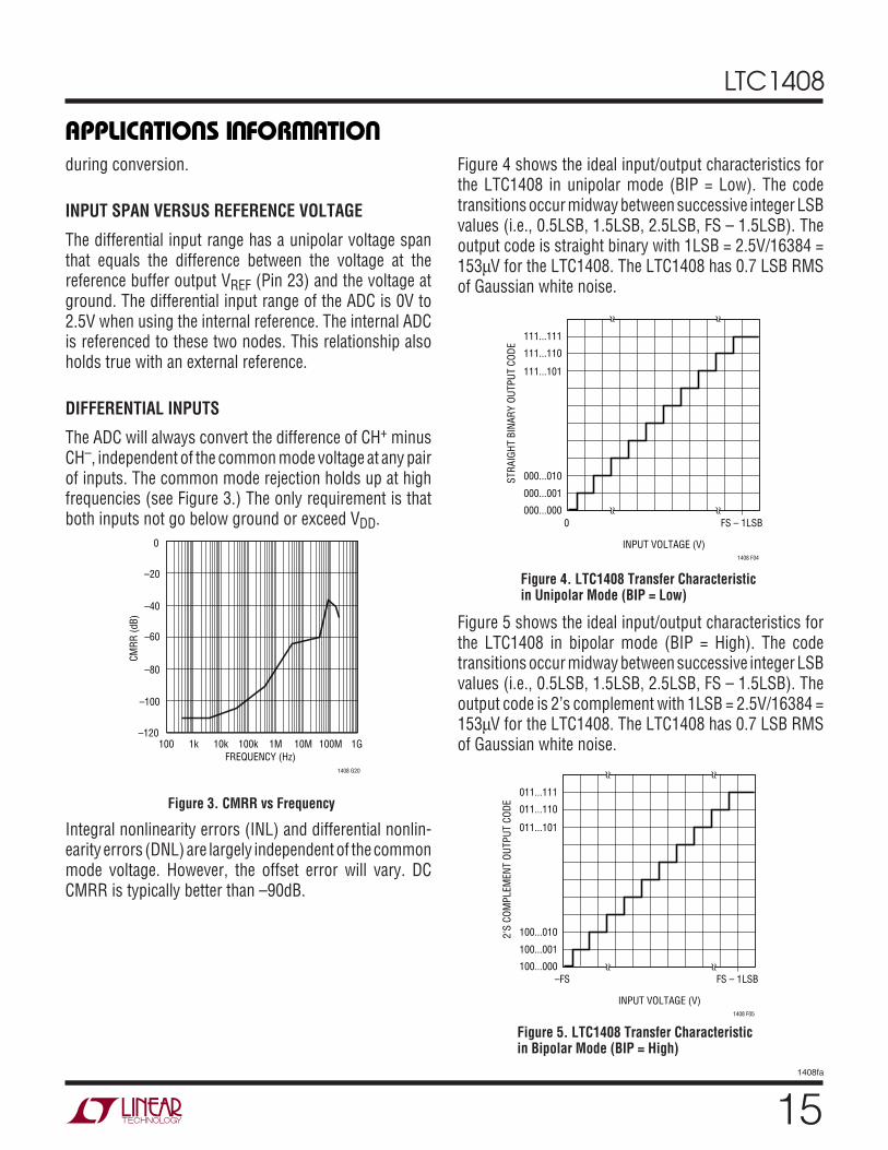
Figure 4 shows the ideal input/output characteristics forthe LTC1408 in unipolar mode (BIP = Low). The codetransitions occur midway between successive integer LSBvalues (i.e., 0.5LSB, 1.5LSB, 2.5LSB, FS – 1.5LSB). Theoutput code is straight binary with 1LSB = 2.5V/16384 =153µV for the LTC1408. The LTC1408 has 0.7 LSB RMSof Gaussian white noise.
during conversion.
INPUT SPAN VERSUS REFERENCE VOLTAGE
The differential input range has a unipolar voltage spanthat equals the difference between the voltage at thereference buffer output VREF (Pin 23) and the voltage atground. The differential input range of the ADC is 0V to2.5V when using the internal reference. The internal ADCis referenced to these two nodes. This relationship alsoholds true with an external reference.
DIFFERENTIAL INPUTS
The ADC will always convert the difference of CH+ minusCH–, independent of the common mode voltage at any pairof inputs. The common mode rejection holds up at highfrequencies (see Figure 3.) The only requirement is thatboth inputs not go below ground or exceed VDD.
Figure 3. CMRR vs Frequency
1408 G20
FREQUENCY (Hz)
–100
CMRR
(dB)
–60
–20
–40
–80
0
10k 100k 1M 10M 100M 1G–120
100 1k
Integral nonlinearity errors (INL) and differential nonlin-earity errors (DNL) are largely independent of the commonmode voltage. However, the offset error will vary. DCCMRR is typically better than –90dB.
Figure 5 shows the ideal input/output characteristics forthe LTC1408 in bipolar mode (BIP = High). The codetransitions occur midway between successive integer LSBvalues (i.e., 0.5LSB, 1.5LSB, 2.5LSB, FS – 1.5LSB). Theoutput code is 2’s complement with 1LSB = 2.5V/16384 =153µV for the LTC1408. The LTC1408 has 0.7 LSB RMSof Gaussian white noise.
Figure 5. LTC1408 Transfer Characteristicin Bipolar Mode (BIP = High)
INPUT VOLTAGE (V)
2'S
COM
PLEM
ENT
OUTP
UT C
ODE
1408 F05
011...111
011...110
011...101
100...000
100...001
100...010
FS – 1LSB–FS
Figure 4. LTC1408 Transfer Characteristicin Unipolar Mode (BIP = Low)
INPUT VOLTAGE (V)
STR
AIGH
T BI
NARY
OUT
PUT
CODE
1408 F04
111...111
111...110
111...101
000...000
000...001
000...010
FS – 1LSB0

16
LTC1408
1408fa
APPLICATIO S I FOR ATIO
WU UU
POWER-DOWN MODES
Upon power-up, the LTC1408 is initialized to the activestate and is ready for conversion. The Nap and Sleep modewaveforms show the power down modes for the LTC1408.The SCK and CONV inputs control the power down modes(see Timing Diagrams). Two rising edges at CONV, with-out any intervening rising edges at SCK, put the LTC1408in Nap mode and the power drain drops from 15mW to3.3mW. The internal reference remains powered in Napmode. One or more rising edges at SCK wake up theLTC1408 for service very quickly and CONV can start anaccurate conversion within a clock cycle. Four risingedges at CONV, without any intervening rising edges atSCK, put the LTC1408 in Sleep mode and the power draindrops from 15mW to 10µW. One or more rising edges atSCK wake up the LTC1408 for operation. The internalreference (VREF ) takes 2ms to slew and settle with a 10µFload. Using sleep mode more frequently compromises theaccuracy of the output data. Note that for slower conver-sion rates, the Nap and Sleep modes can be used forsubstantial reductions in power consumption.
DIGITAL INTERFACE
The LTC1408 has a 3-wire SPI (Serial Peripheral Interface)interface. The SCK and CONV inputs and SDO outputimplement this interface. The SCK and CONV inputsaccept swings from 3V logic and are TTL compatible, if thelogic swing does not exceed VDD. A detailed description ofthe three serial port signals follows:
Conversion Start Input (CONV)
The rising edge of CONV starts a conversion, but subse-quent rising edges at CONV are ignored by the LTC1408until the following 96 SCK rising edges have occurred. Theduty cycle of CONV can be arbitrarily chosen to be used asa frame sync signal for the processor serial port. A simpleapproach to generate CONV is to create a pulse that is oneSCK wide to drive the LTC1408 and then buffer this signalto drive the frame sync input of the processor serial port.It is good practice to drive the LTC1408 CONV input firstto avoid digital noise interference during the sample-to-hold transition triggered by CONV at the start of conver-sion. It is also good practice to keep the width of the lowportion of the CONV signal greater than 15ns to avoidintroducing glitches in the front end of the ADC just beforethe sample-and-hold goes into Hold mode at the risingedge of CONV.

17
LTC1408
1408fa
APPLICATIO S I FOR ATIO
WU UU
Minimizing Jitter on the CONV Input
In high speed applications where high amplitude sinewavesabove 100kHz are sampled, the CONV signal must have aslittle jitter as possible (10ps or less). The square waveoutput of a common crystal clock module usually meetsthis requirement easily. The challenge is to generate aCONV signal from this crystal clock without jitter corrup-tion from other digital circuits in the system. A clockdivider and any gates in the signal path from the crystalclock to the CONV input should not share the sameintegrated circuit with other parts of the system. The SCKand CONV inputs should be driven first, with digital buffersused to drive the serial port interface. Also note that themaster clock in the DSP may already be corrupted withjitter, even if it comes directly from the DSP crystal.Another problem with high speed processor clocks is thatthey often use a low cost, low speed crystal (i.e., 10MHz)to generate a fast, but jittery, phase-locked-loop systemclock (i.e., 40MHz). The jitter in these PLL-generated highspeed clocks can be several nanoseconds. Note that if youchoose to use the frame sync signal generated by the DSPport, this signal will have the same jitter of the DSP’smaster clock.
The Typical Application Figure on page 20 shows a circuitfor level-shifting and squaring the output from an RFsignal generator or other low-jitter source. A single D-typeflip flop is used to generate the CONV signal to theLTC1408. Re-timing the master clock signal eliminatesclock jitter introduced by the controlling device (DSP,FPGA, etc.) Both the inverter and flip flop must be treatedas analog components and should be powered from aclean analog supply.
Serial Clock Input (SCK)
The rising edge of SCK advances the conversion processand also udpates each bit in the SDO data stream. AfterCONV rises, the third rising edge of SCK sends out up tosix sets of 14 data bits, with the MSB sent first. A simpleapproach is to generate SCK to drive the LTC1408 first andthen buffer this signal with the appropriate number ofinverters to drive the serial clock input of the processorserial port. Use the falling edge of the clock to latch datafrom the Serial Data Output (SDO) into your processorserial port. The 14-bit Serial Data will be received rightjustified, in six 16-bit words with 96 or more clocks perframe sync. If fewer than 6 channels are selected bySEL0–SEL2 for conversion, then 16 clocks are needed perchannel to convert the analog inputs and read out theresulting data after the next convert pulse. It is goodpractice to drive the LTC1408 SCK input first to avoiddigital noise interference during the internal bit compari-son decision by the internal high speed comparator.Unlike the CONV input, the SCK input is not sensitive tojitter because the input signal is already sampled and heldconstant.
Serial Data Output (SDO)
Upon power-up, the SDO output is automatically resetto the high impedance state. The SDO output remainsin high impedance until a new conversion is started.SDO sends out up to six sets of 14 bits in the output datastream after the third rising edge of SCK after the startof conversion with the rising edge of CONV. The six orfewer 14-bit words are separated by two clock cycles inhigh impedance mode. Please note the delay specifica-tion from SCK to a valid SDO. SDO is always guaranteedto be valid by the next rising edge of SCK. The 16 – 96-bit output data stream is compatible with the 16-bit or32-bit serial port of most processors.

18
LTC1408
1408fa
APPLICATIO S I FOR ATIO
WU UU1408 F06
3
30
32
1
2
3-WIRE SERIALINTERFACE LINK
OVDD
CONV
SCK
LTC1408
SDO
VCC
BFSR
BCLKR
TMS320C54x
BDR
OGND
31DGND
CONV
0V TO 3V LOGIC SWING
CLK
5V3V
B13 B12
Figure 7. DSP Serial Interface to TMS320C54x
BOARD LAYOUT AND BYPASSING
Wire wrap boards are not recommended for high resolu-tion and/or high speed A/D converters. To obtain the bestperformance from the LTC1408, a printed circuit boardwith ground plane is required. Layout for the printed circuitboard should ensure that digital and analog signal lines areseparated as much as possible. In particular, care shouldbe taken not to run any digital track alongside an analogsignal track. If optimum phase match between the inputsis desired, the length of the twelve input wires of the sixinput channels should be kept matched. But each pair ofinput wires to the six input channels should be keptseparated by a ground trace to avoid high frequencycrosstalk between channels.
High quality tantalum and ceramic bypass capacitors shouldbe used at the VCC, VDD and VREF pins as shown in the BlockDiagram on the first page of this data sheet. For optimumperformance, a 10µF surface mount tantalum capacitorwith a 0.1µF ceramic is recommended for the VCC, VDD andVREF pins. Alternatively, 10µF ceramic chip capacitors suchas X5R or X7R may be used. The capacitors must be lo-cated as close to the pins as possible. The traces connect-ing the pins and the bypass capacitors must be kept shortand should be made as wide as possible. The VCC and VDDbypass capacitor returns to the ground plane and the VREFbypass capacitor returns to the Pin 22. Care should betaken to place the 0.1µF VCC and VDD bypass capacitor asclose to Pins 24 and 25 as possible.
Figure 6. Recommended Layout
Figure 6 shows the recommended system ground connec-tions. All analog circuitry grounds should be terminated atthe LTC1408 Exposed Pad. The ground return from theLTC1408 to the power supply should be low impedance fornoise-free operation. The Exposed Pad of the 32-pin QFNpackage is also internally tied to the ground pads. TheExposed Pad should be soldered on the PC board to reduceground connection inductance. All ground pins (GND,DGND, OGND) must be connected directly to the sameground plane under the LTC1408.
VDD BYPASS,0.1µF, 0402
OVDD BYPASS,0.1µF, 0402
VREF BYPASS,10µF, 0805
VCC BYPASS,0.1µF, 0402 AND10µF, 0805
HARDWARE INTERFACE TO TMS320C54x
The LTC1408 is a serial output ADC whose interface hasbeen designed for high speed buffered serial ports in fastdigital signal processors (DSPs). Figure 7 shows anexample of this interface using a TMS320C54X.
The buffered serial port in the TMS320C54x has directaccess to a 2kB segment of memory. The ADC’s serial datacan be collected in two alternating 1kB segments, in realtime, at the full 600ksps conversion rate of the LTC1408.The DSP assembly code sets frame sync mode at the BFSRpin to accept an external positive going pulse and the serialclock at the BCLKR pin to accept an external positive edgeclock. Buffers near the LTC1408 may be added to drivelong tracks to the DSP to prevent corruption of the signalto LTC1408. This configuration is adequate to traverse atypical system board, but source resistors at the bufferoutputs and termination resistors at the DSP, may beneeded to match the characteristic impedance of very longtransmission lines. If you need to terminate the SDOtransmission line, buffer it first with one or two 74ACxxgates. The TTL threshold inputs of the DSP port respondproperly to the 3V swing used with the LTC1408.

19
LTC1408
1408fa
U
PACKAGE DESCRIPTIO
Information furnished by Linear Technology Corporation is believed to be accurate and reliable.However, no responsibility is assumed for its use. Linear Technology Corporation makes no represen-tation that the interconnection of its circuits as described herein will not infringe on existing patent rights.
5.00 ± 0.10(4 SIDES)
NOTE:1. DRAWING PROPOSED TO BE A JEDEC PACKAGE OUTLINE M0-220 VARIATION WHHD-(X) (TO BE APPROVED)2. DRAWING NOT TO SCALE3. ALL DIMENSIONS ARE IN MILLIMETERS4. DIMENSIONS OF EXPOSED PAD ON BOTTOM OF PACKAGE DO NOT INCLUDE MOLD FLASH. MOLD FLASH, IF PRESENT, SHALL NOT EXCEED 0.20mm ON ANY SIDE5. EXPOSED PAD SHALL BE SOLDER PLATED6. SHADED AREA IS ONLY A REFERENCE FOR PIN 1 LOCATION ON THE TOP AND BOTTOM OF PACKAGE
PIN 1TOP MARK(NOTE 6)
0.40 ± 0.10
31
1
2
32
BOTTOM VIEW—EXPOSED PAD
3.45 ± 0.10(4-SIDES)
0.75 ± 0.05 R = 0.115TYP
0.25 ± 0.05(UH32) QFN 1004
0.50 BSC
0.200 REF
0.00 – 0.05
0.70 ±0.05
3.45 ±0.05(4 SIDES)
4.10 ±0.05
5.50 ±0.05
0.25 ± 0.05
PACKAGE OUTLINE
0.50 BSC
RECOMMENDED SOLDER PAD LAYOUT
PIN 1 NOTCH R = 0.30 TYPOR 0.35 × 45° CHAMFER
UH Package32-Lead Plastic QFN (5mm × 5mm)
(Reference LTC DWG # 05-08-1693)

20
LTC1408
1408fa
RELATED PARTS
© LINEAR TECHNOLOGY CORPORATION 2006
LT 0606 • PRINTED IN THE USALinear Technology Corporation1630 McCarthy Blvd., Milpitas, CA 95035-7417(408) 432-1900 FAX: (408) 434-0507 www.linear.com
PART NUMBER DESCRIPTION COMMENTS
ADCsLTC1402 12-Bit, 2.2Msps Serial ADC 5V or ±5V Supply, 4.096V or ±2.5V SpanLTC1403/LTC1403A 12-/14-Bit, 2.8Msps Serial ADC 3V, 15mW, Unipolar Inputs, MSOP PackageLTC1403-1/LTC1403A-1 12-/14-Bit, 2.8Msps Serial ADC 3V, 15mW, Bipolar Inputs, MSOP PackageLTC1405 12-Bit, 5Msps Parallel ADC 5V, Selectable Spans, 115mWLTC1407/LTC1407A 12-/14-Bit, 3Msps Simultaneous Sampling ADC 3V, 14mW, 2-Channel Unipolar Input RangeLTC1407-1/LTC1407A-1 12-/14-Bit, 3Msps Simultaneous Sampling ADC 3V, 14mW, 2-Channel Bipolar Input RangeLTC1411 14-Bit, 2.5Msps Parallel ADC 5V, Selectable Spans, 80dB SINADLTC1412 12-Bit, 3Msps Parallel ADC ±5V Supply, ±2.5V Span, 72dB SINADLTC1420 12-Bit, 10Msps Parallel ADC 5V, Selectable Spans, 72dB SINADLTC1608 16-Bit, 500ksps Parallel ADC ±5V Supply, ±2.5V Span, 90dB SINADLTC1609 16-Bit, 250ksps Serial ADC 5V Configurable Bipolar/Unipolar InputsLTC1864/LTC1865 16-Bit, 250ksps 1-/2-Channel Serial ADCs 5V or 3V (L-Version), Micropower, MSOP PackageLTC1864L/LTC1865LDACsLTC1592 16-Bit, Serial SoftSpanTM IOUT DAC ±1LSB INL/DNL, Software Selectable SpansLTC1666/LTC1667 12-/14-/16-Bit, 50Msps DAC 87dB SFDR, 20ns Settling TimeLTC1668ReferencesLT1460-2.5 Micropower Series Voltage Reference 0.10% Initial Accuracy, 10ppm DriftLT1461-2.5 Precision Voltage Reference 0.04% Initial Accuracy, 3ppm DriftLT1790-2.5 Micropower Series Reference in SOT-23 0.05% Initial Accuracy, 10ppm DriftSoftSpan is a trademark of Linear Technology Corporation.
U
TYPICAL APPLICATIO
PRE
VCC
1k
1k50Ω
VCC
NL17SZ74 CONVERT ENABLE
NC7SVU04P5X
MASTER CLOCK0.1µF
TO LTC1408CONV
CONTROLLOGIC
(FPGA, CPLD,DSP, ETC.)
D Q
Q
CLR
1408 TA02
Clock Squaring/Level Shifting Circuit Allows Testing with RF Sine Generator.Convert Re-Timing Flip-Flop Preserves Low-Jitter Clock Timing
Top Related