


Languages
Pages
Legal


AURORA'S ENGINEERING COLLEGE
Bhuvanagiri, Nalgonda Dist.-508116.
ENGINEERING PHYSICS
LAB MANUAL
B.Tech. 1st Year
(As per 2013 Academic Regulation)
Department of
HUMANITIES & SCIENCES
COMMON TO
CSE, ECE, EEE, IT, MECH & CIVIL
Physics Lab Manual Aurora’s Engineering College
1
CODE OF CONDUCT
1. Students should report to the concerned lab as per the time-table schedule.
2. Students who turn up late to the labs will in no case be permitted to
perform the experiment scheduled for the day. 3 After completion of the experiment, certification of the concerned staff in-
charge in the observation book is necessary. 4. Students should bring a note book of about 100 pages and should enter
the readings / observations into the note book while performing the experiment.
5. The record of observations along with the detailed experimental procedure
of the experiment performed in the immediate last session should be submitted and certified by the staff member in-charge.
6. The group-wise division made in the beginning should be adhered to, and
no mix up of students among different groups will be permitted later.
7. The components required pertaining to the experiment should be collected
from stores in-charge after duly filling in the requisition form.
8. When the experiment is completed, students should disconnect the setup
made by them, and should return all the components/instruments taken for the purpose.
9. Any damage to apparatus that occurs during the experimentation, should
be brought to the notice of lab in-charge, consequently, the cost of the repair or new apparatus should be brought by the students.
10. Students should be present in the labs for the total scheduled duration. 11. Students are required to prepare thoroughly to perform the experiment
before coming to Laboratory. 12. Procedure sheets/data sheets provided to the students’ groups should be
maintained neatly and to be returned after the experiment.

Physics Lab Manual Aurora’s Engineering College
2
CONTENTS
S.No Name of the Experiment Page No.
1. DISPERSIVE POWER OF THE MATERIAL OF A
PRISM – SPECTROMETER. 3
2. DETERMINATION OF WAVELENGTH OF A
SOURCE – DIFFRACTION GRATING. 9
3. NEWTON’S RINGS - RADIUS OF CURVATURE OF
PLANO CONVEX LENS. 14
4. MELDE’S EXPERIMENT – TRANSVERSE AND
LONGITUDINAL MODES. 20
5. TIME CONSTANT OF AN R-C CIRCUIT. 27
6. L-C-R CIRCUIT. 34
7.
MAGNETIC FIELD ALONG THE AXIS OF CURRENT CARRYING COIL – STEWART AND
GEES METHOD. 42
8. STUDY THE CHARACTERISTICS OF LED AND
LASER SOURCES. 48
9. STUDY THE CHARACTERISTICS OF P-I-N AND
AVALANCHE PHOTODIODE DETECTORS. 53
10. BENDING LOSSES OF FIBRES. 63
11. EVALUATION OF NUMERICAL APERTURE OF
GIVEN FIBRE. 69
12. ENERGY GAP OF A MATERIAL OF P-N
JUNCTION. 75
13. TORSIONAL PENDULUM. 81
14. SINGLE SLIT DIFFRACTION USING LASER. 88
15 CHARACTERISTICS OF A SOLAR CELL 95

Physics Lab Manual Aurora’s Engineering College
3
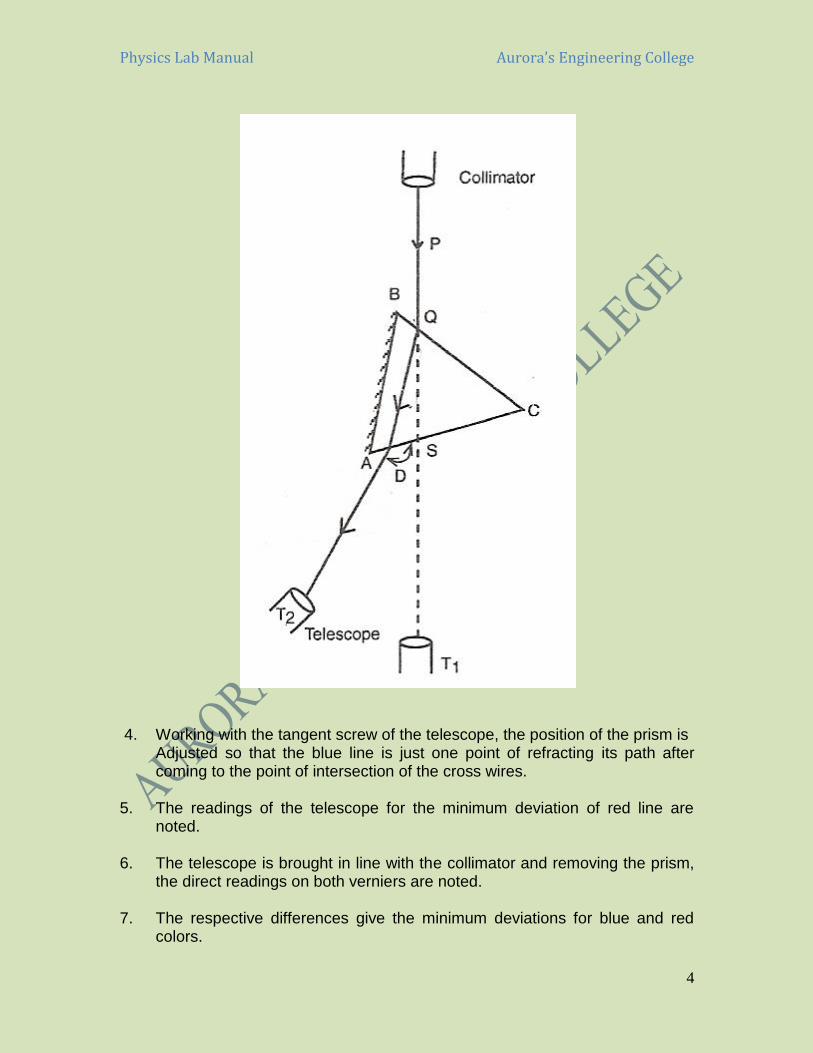
1. DISPERSIVE POWER OF THE MATERIAL OF A PRISM – SPECTROMETER.
AIM: - To determine the dispersive power of the material of a given prism by the spectrometer APPARATUS: - Spectrometer, Prism and Mercury Vapour Lamp PRINCIPLE: - The Dispersive power of the material of the given prism is expressed as
=(2−1)
(−1)
Where 1 and 2 are the refractive indices of two colors
=(
1+
2)
2
Usually the colors chosen are blue and red so that
=(
𝑏−
𝑟)
( − 1),
Where = (𝑏+ 𝑟)
2
PROCEDURE: - 1. The usual adjustments of the spectrometer are made .The refractive angle
of the Prism is found. 2. Then the prism is mounted on the prism table and the position of prism is
adjusted to observe the spectrum of the mercury vapor. 3. Observing the blue line in the spectrum through the telescope, the prism is
adjusted for minimum deviation position.
Physics Lab Manual Aurora’s Engineering College
4
4. Working with the tangent screw of the telescope, the position of the prism is Adjusted so that the blue line is just one point of refracting its path after
coming to the point of intersection of the cross wires. 5. The readings of the telescope for the minimum deviation of red line are
noted. 6. The telescope is brought in line with the collimator and removing the prism,
the direct readings on both verniers are noted. 7. The respective differences give the minimum deviations for blue and red
colors.

Physics Lab Manual Aurora’s Engineering College
5
Their refractive indices are found by
𝜇𝑏 = 𝑆𝑖𝑛(𝐴 + 𝐷𝑏)
2
𝑆𝑖𝑛 (𝐴/2) & 𝜇𝑟 =
𝑆𝑖𝑛(𝐴 + 𝐷𝑟)2
𝑆𝑖𝑛 (𝐴/2)
The Dispersive power of the material of the prism, for blue and red colors is found by the relation
=(
𝑏−
𝑟)
( − 1),
OBSERVATIONS: - The observations of the above experiment are as follows
V1 = MSR0+ (LC’) VC
Spectral Line
Direct
Reading
Minimum Deviation Position
Angle of Min. Deviation
𝜇
= 𝑆𝑖𝑛(𝐴 + 𝐷𝑚)
2
𝑆𝑖𝑛 (𝐴/2) LHS
V1
RHS V2
LHS V1’
RHS V2’
Dm(LHS) |𝑉1 − 𝑉′1|
Dm(RHS)
|𝑉2 − 𝑉′2|
AVG Dm
Blue Green Yellow Red
Dispersive power =(𝑏− 𝑟)
(−1)

Physics Lab Manual Aurora’s Engineering College
6
PRECAUTIONS: - 1. The prism should be adjusted for each colour separately. 2. Readings are noted without any parallax error. RESULT: - The Dispersive power of the material of the prism =----------------
REFERENCE BOOKS:-
1.”Fundamentals of physics” D.Halliday,R.Resnick and J.walker,John wiley and sons.New York 2001 2.PHYSICS”,M.Alonso and E.J.Finn,Addison Wesley, 1992 3.”LABORATORY MANUAL IN APPLIED PHYSICS” -Second edition-H.Sathyaseelam-New age International

Physics Lab Manual Aurora’s Engineering College
7

Physics Lab Manual Aurora’s Engineering College
8
Physics Lab Manual Aurora’s Engineering College
9
2. DETERMINATION OF WAVELENGTH OF A SOURCE – DIFFRACTION GRATING.
AIM: - To determine the wavelength of light using a plane diffraction grating by measuring the Angle of minimum deviation. APPARATUS: - Plane diffraction grating, spectrometer, reading lens, sodium vapor lamp. PRINCIPLE: - If a parallel beam of monochromatic light is incident on a grating, such that the angle of deviation is minimum, the relation gives the wavelength of the light.
𝜆 =2 sin(𝐷
2)
𝑁𝑛
Where D is the angle of minimum deviation
n is the order of the spectrometer and N is the number of lines per cm
PROCEDURE: - 1 The preliminary adjustments of the spectrometer are done. The slit is
illuminated with Sodium light. 2. The grating is clamped to the prism table. The plane of the grating is
adjusted to be Vertical and perpendicular to the axis of the collimator. 3. The direct image of the slit is observed through telescope and by fine
adjustment of the tangent Screw of the telescope, the point of intersection of the cross wire is set on the image of the slit. The readings of the two verniers are noted.
4. The telescope is moved to the left to observe the diffracted image of the first order.
5. The prism table is released and is rotated to the left. Then the first order image moves. To the right, reaches a limiting position, and then tries to retrace its path.
6. The telescope is fixed in this limiting position such that the point of intersection of the Cross wire is on the D1 line. The readings on both the verniers are noted.
7. The respective difference on the verniers gives the minimum deviation for the D1 line. Similarly the experiment is repeated on the right hand side for the first order D1 line. The experiment is repeated for D2 line.

Physics Lab Manual Aurora’s Engineering College
10
OBSERVATIONS: - The observations of the experiment are as follows
Least count of spectrometer = 1 𝑀𝑆𝐷
𝑁𝑜 𝑑𝑖𝑣 𝑖𝑛 𝑣𝑒𝑟𝑛𝑖𝑒𝑟 𝑠𝑐𝑎𝑙𝑒
No. Of lines per cm. on the grating (N) = Table
Spectral line
Direct reading
Minimum deviation position Angle of minimum deviation
Dm
Mean Dm=
Left side Right side
n R1 R2 R’1 R’2 R”1 R”2 |𝐴 − 𝐶| |𝐵 − 𝐷| |𝐴 − 𝐸| |𝐵 − 𝐹|
A B C D E F G H I J
1
2
Physics Lab Manual Aurora’s Engineering College
11
Calculations
𝜆 =2 sin(𝐷
2)
𝑁𝑛
Where D is the angle of minimum deviation
n is the order of the spectrometer and N is the number of lines per cm
PRECAUTIONS: - 1. The grating should be adjusted for each order separately. 2. Readings are noted without any parallax error. RESULT: -
Wave length of sodium is -----------------A0 (Ist order) Wave length of sodium is -----------------A0 (IInd order)
REFERENCE BOOKS:-
1.”THE FEYNMAN LECTURES IN PHYSICS”,R.P.Feynman,R.B. Leighton and M.Sands,Addison Wesley ,1963 2.”FUNDAMENTALS OF PHYSICS”,4th edition ,F.A.Jenkins and H.E.White, 1981 3.”OPTICS”,A.GHATAK, Tata McGraw Hill ,New delhi,1992 4.”LABORATORY MANUAL IN APPLIED PHYSICS” -Second edition-H.Sathyaseelam-New age International

Physics Lab Manual Aurora’s Engineering College
12

Physics Lab Manual Aurora’s Engineering College
13

Physics Lab Manual Aurora’s Engineering College
14
3. NEWTON’S RINGS - RADIUS OF CURVATURE OF PLANO CONVEX LENS.
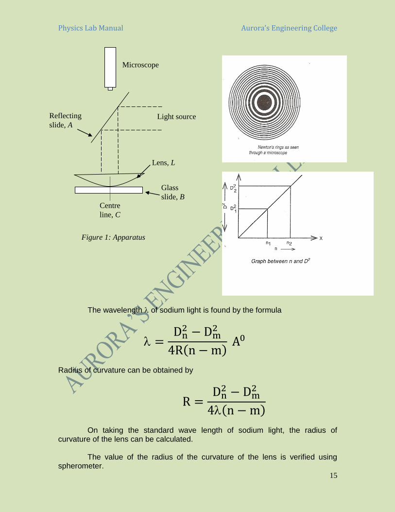
AIM: - To determine of Radius of curvature of a Plano convex lens by Newton’s rings method. APPARATUS: - A convex lens is focal length about 100 cm, two optically plane glass plates, and traveling micro scope, a condensing lens and sodium Vapor lamp. DESCRIPTION: - The convex lens is placed on the optically plane plate B as shown in the below fig .On the platform of the traveling microscope. A black paper is placed under the glass plate.
The condensing lens C is placed at a distance equal to the focal length of the lens from the sodium Vapor lamps. The emergent parallel beam of the light is directed towards the glass plate A kept directly above the center of the lens and inclined at 450 to the vertical. The beam of light is reflected on the lens L. As a result of interference between the light reflected from the lower surface of the lens and the top surface of the glass plate B. Newton’s rings with alternate bright and dark rings are formed having a black center. The microscope can focus these rings. (It may happen that the center of the ring system is bright. This is due to the presence of dust particles between the lens and the thick glass plate. In such a case the surface of the lens and the glass plate has to be cleaned.) PROCEDURE: - The microscope is focused at the center of the ring system. The microscope is moved so that the cross wires pass over 16 or 17 dark rings. Then the microscope is moved back until the vertical cross wire is set at the middle (or end) of the 15th dark ring. The reading of the main scale and the number of Vernier coincidences are noted from which the reading of the microscope can be determined. The microscope is moved so that the vertical cross wire is set at the middle of the 14th dark ring. The readings of the microscope are noted. Similarly the readings of the microscope with crosswire set Successively at the middle of 13th, 12th, 11th etc…………..5th dark ring. The microscope corresponding to 5th, 6th, 7th …. 15th dark ring on the other side of the center are noted. From these observations the diameters of the 5th, 6th, etc………15th dark rings can be found.
The convex lens L is removed and its radius of curvature R is determined either by a spherometer or by Boy’s method.
A graph is drawn with number of the dark ring on the x-axis and the square of the diameter (D2) on the y-axis. The graph is a straight line passing through origin. From the graph the values of Dm
2 and Dn2 corresponding to nth
and mth rings are found.
Physics Lab Manual Aurora’s Engineering College
15
The wavelength of sodium light is found by the formula
=Dn
2 − Dm2
4R(n − m) A0
Radius of curvature can be obtained by
R =Dn
2 − Dm2
4(n − m)
On taking the standard wave length of sodium light, the radius of
curvature of the lens can be calculated. The value of the radius of the curvature of the lens is verified using
spherometer.
Light source
Microscope
Reflecting
slide, A
Lens, L
Glass
slide, B Centre
line, C
Figure 1: Apparatus
Physics Lab Manual Aurora’s Engineering College
16
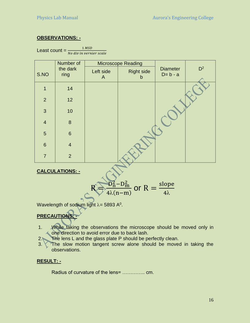
OBSERVATIONS: -
Least count = 1 𝑀𝑆𝐷
𝑁𝑜 𝑑𝑖𝑣 𝑖𝑛 𝑣𝑒𝑟𝑛𝑖𝑒𝑟 𝑠𝑐𝑎𝑙𝑒
S.NO
Number of the dark ring
Microscope Reading Diameter D= b - a
D2
Left side A
Right side b
1
2
3
4
5
6
7
14
12
10
8
6
4
2
CALCULATIONS: -
R =Dn
2 −Dm2
4(n−m) or R =
slope
4
Wavelength of sodium light = 5893 A0. PRECAUTIONS: - 1. While taking the observations the microscope should be moved only in
one direction to avoid error due to back lash. 2. The lens L and the glass plate P should be perfectly clean. 3. The slow motion tangent screw alone should be moved in taking the
observations. RESULT: - Radius of curvature of the lens= ………….. cm.

Physics Lab Manual Aurora’s Engineering College
17
REFERENCE BOOKS:-
1.”FUNDAMENTALS OF PHYSICS”,D.Halliday,R.Resnick and J.Walkar,John wiley and sons,New York,2001 2.”VIBRATIONS AND WAVES”,A.P.French,Arnold-Heinemann,New Delhi,1972 3.”BASIC ELECTRONIC INSTRUMENT” Hand Book ,C.F.Coombs,McGraw-Hill ,1972 4.”LABORATORY MANUAL IN APPLIED PHYSICS” -Second edition-H.Sathyaseelam-New age International

Physics Lab Manual Aurora’s Engineering College
18

Physics Lab Manual Aurora’s Engineering College
19
Physics Lab Manual Aurora’s Engineering College
20
4. MELDE’S EXPERIMENT – TRANSVERSE AND LONGITUDINAL MODES.
AIM: - To determine the frequency of an electrically driven tuning fork. APPARATUS: - An electrically maintained tuning fork ,a light smooth pulley fixed to a stand, a light scale pan, thread, a storage cell, rheostat, plug key and connecting wires. DESCRIPTION: - A fork can be maintained in the state of continuous vibration electrically. One terminal of the coil of an electromagnet is connected to the make and break arrangement and the other end of the coil to the cell, rheostat and plug key connected in series. In the normal position when the circuit is closed, the electromagnet attracts the prong of the fork towards it. This breaks electrical circuit and the prong moves back closing the circuit. The electromagnet again attracts the prong towards it. This is repeated again and again and the fork is maintained in a state of continuous vibration. One end of the thread of length about 3 meters is joined to a screw attached to one prong of the fork and the other end is passed over a small pulley and a light pan is fixed at the other end of the thread. When the fork is vibrated electrically, stationary waves of well-defined loops are formed. Melde’s apparatus can be arranged in two modes of vibration, TRANSVERSE MODE
When the direction of motion of the prong is at right angles to the length of the string, the vibrations of the thread represent the transverse mode of vibration. PROCEDURE: - 1) The apparatus is arranged in transverse mode of vibration of the thread as shown above. A suitable load is placed in the scale pan. The tuning fork is excited electrically. The length of the thread is adjusted by moving the pulley until well defined loops are formed in it. The distance between a definite numbers of well-defined loops is measured with a meter scale from which the average length
l of a single loop is determined. 2) The total load attached to the thread inclusive of the mass of the pan is noted. If it is M gm, the tension applied on the string is T= Mg = (M’+M”) g. Where g is acceleration due to gravity. M’ is the mass added in the pan and M” is the mass of pan. 3) The mass of the thread (about 5 mts in length) is determined correct to a milligram. The mass per unit length of the string (m) is then determined. The frequency of the tuning fork is found by the relation

Physics Lab Manual Aurora’s Engineering College
21
l
T
mm
T
lN
2
1
2
1
4) The experiment is repeated for various tensions and the observations are tabulated in table (i) and N is calculated

Physics Lab Manual Aurora’s Engineering College
22
OBSERVATIONS:
Average l
T = ……………
M’ = mass kept in the pan in grams M” = mass of the pan m = linear density
Formula for calculation 𝑁 = 1
2√𝑚(𝐴𝑣𝑒𝑟𝑎𝑔𝑒
√𝑇
𝑙)
Longitudinal Mode When the direction of motion of the prong is along the length of the thread, the vibrations of the thread represent longitudinal mode of vibration. PROCEDURE: - 1) The apparatus is arranged in longitudinal mode of vibration of the thread. The
experiment is done in similar manner as in 1. The average l of the loop, the
tension T applied to the thread and the mass per unit length of the thread (m) are found. The frequency of the tuning fork is found by the relation
l
T
mm
T
lN
11
S.No
M’ T=Mg
= (M’+M”)g No. of
loops P Total length L
Length of each loop
l = L/P l
T

Physics Lab Manual Aurora’s Engineering College
23
The experiment is repeated with different tension and the observations are tabulated in table (ii) and are calculated. OBSERVATIONS:
Average l
T = ……
Mass per unit length of the thread (m) = …………… gms. M’ = mass kept in the pan in grams M” = mass of the pan m = linear density
Formula for calculation 𝑁 = 1
√𝑚(𝐴𝑣𝑒𝑟𝑎𝑔𝑒
√𝑇
𝑙)
PRECAUTIONS: - 1) A thin long and inelastic thread should be used. 2) The loops should be well defined and confined to a single plane. RESULT: The frequency of the tuning fork in transverse mode = ………… Hz The frequency of the tuning fork in longitudinal mode = ………… Hz The mean of the two average frequencies in the transverse and longitudinal modes gives the correct frequency of the tuning fork.
S.No
M’ T=Mg
= (M’+M”)g No.of
loops P Total length L
Length of each loop
l = L/P l
T
Physics Lab Manual Aurora’s Engineering College
24
REFERENCE BOOKS:- 1.”LABORATORY EXPERIMENTS IN COLLEGE PHYSICS”,C.H.Bernard and C.D.Epp.John Wiley and Sons Inc.,New York 1995 2.”THE FEYNMAN LECTURES IN PHYSICS”,R.P.Feynman,R.B.Leighton and M.Sands,Addison Wesley,1963 3.”OPTICS”,A.Ghatak, Tata-McGraw Hill,New delhi,1992 4.”LABORATORY MANUAL IN APPLIED PHYSICS” -Second edition-H.Sathyaseelam-New age International
Physics Lab Manual Aurora’s Engineering College
25

Physics Lab Manual Aurora’s Engineering College
26
Physics Lab Manual Aurora’s Engineering College
27
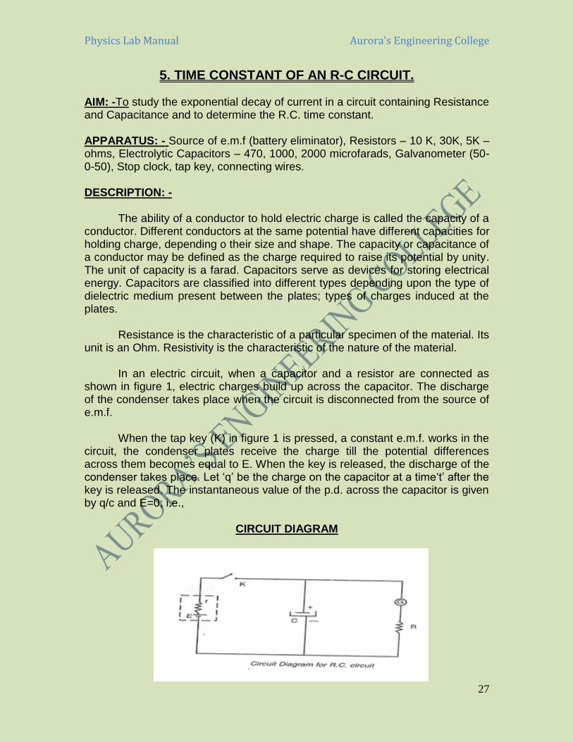
5. TIME CONSTANT OF AN R-C CIRCUIT. AIM: -To study the exponential decay of current in a circuit containing Resistance and Capacitance and to determine the R.C. time constant. APPARATUS: - Source of e.m.f (battery eliminator), Resistors – 10 K, 30K, 5K – ohms, Electrolytic Capacitors – 470, 1000, 2000 microfarads, Galvanometer (50-0-50), Stop clock, tap key, connecting wires. DESCRIPTION: - The ability of a conductor to hold electric charge is called the capacity of a conductor. Different conductors at the same potential have different capacities for holding charge, depending o their size and shape. The capacity or capacitance of a conductor may be defined as the charge required to raise its potential by unity. The unit of capacity is a farad. Capacitors serve as devices for storing electrical energy. Capacitors are classified into different types depending upon the type of dielectric medium present between the plates; types of charges induced at the plates.
Resistance is the characteristic of a particular specimen of the material. Its unit is an Ohm. Resistivity is the characteristic of the nature of the material. In an electric circuit, when a capacitor and a resistor are connected as shown in figure 1, electric charges build up across the capacitor. The discharge of the condenser takes place when the circuit is disconnected from the source of e.m.f. When the tap key (K) in figure 1 is pressed, a constant e.m.f. works in the circuit, the condenser plates receive the charge till the potential differences across them becomes equal to E. When the key is released, the discharge of the condenser takes place. Let ‘q’ be the charge on the capacitor at a time‘t’ after the key is released. The instantaneous value of the p.d. across the capacitor is given by q/c and E=0; i.e.,
CIRCUIT DIAGRAM
Physics Lab Manual Aurora’s Engineering College
28
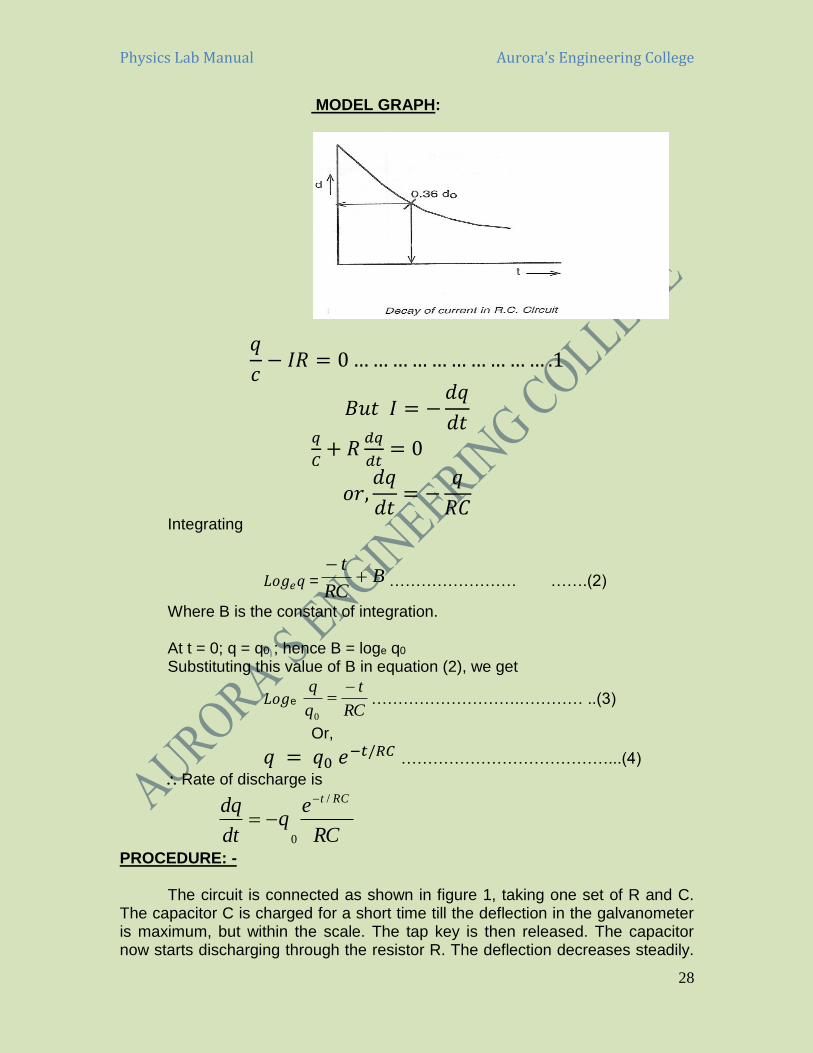
MODEL GRAPH:
𝑞
𝑐− 𝐼𝑅 = 0 … … … … … … … … … … .1
𝐵𝑢𝑡 𝐼 = −𝑑𝑞
𝑑𝑡
𝑞
𝐶+ 𝑅
𝑑𝑞
𝑑𝑡= 0
𝑜𝑟,𝑑𝑞
𝑑𝑡= −
𝑞
𝑅𝐶
Integrating
𝐿𝑜𝑔𝑒𝑞 = BRC
t
…………………… …….(2)
Where B is the constant of integration. At t = 0; q = q0 ; hence B = loge q0
Substituting this value of B in equation (2), we get
𝐿𝑜𝑔e RC
t
q
q
0
……………………….………… ..(3)
Or,
𝑞 = 𝑞0 𝑒−𝑡/𝑅𝐶 …………………………………...(4)
Rate of discharge is
RC
eq
dt
dq RCt /
0
PROCEDURE: - The circuit is connected as shown in figure 1, taking one set of R and C. The capacitor C is charged for a short time till the deflection in the galvanometer is maximum, but within the scale. The tap key is then released. The capacitor now starts discharging through the resistor R. The deflection decreases steadily.

Physics Lab Manual Aurora’s Engineering College
29
The stop clock is started at a suitable initial point (need not be maximum) and the deflection is noted at suitable intervals of time. It is continued till the deflection falls below 0.36 of starting value. The experiment is repeated for the other sets of R and C and the observations are tabulated in Table 1. The time constant is calculated theoretically from the values of R & C used, and also from the graphs; as shown in figure. 2. OBSERVATIONS:
Table.1
S.No.
Time Set 1
R1= ------Ω C1=------µf
Time Set 2
R2 = ------Ω C2 =------µf
Time Set 3 R3 = ------
Ω C3 =------µf
sec Voltage or current
Sec Voltage or current
sec Voltage or current

Physics Lab Manual Aurora’s Engineering College
30
𝐼 = 𝐼 0𝑒𝑥𝑝 (−1) 𝐼 = 0.36 𝐼0
Thus, it is to be observed. (i) Smaller is the time constant; more rapid is the discharge of the capacitor (ii) The current in a R.C. Circuit falls exponentially with time. PRECAUTIONS:- 1. The circuit connection should be done properly. 2. switching on the stop clock and discharging of the capacitor should be done simultaneously RESULT: -
RC time constant Ttheoretical= RXC Ppractical(from Graph)
R1= ------Ω C1=------µf
R2= ------Ω C2=------µf
R3= ------Ω C3=------µf

Physics Lab Manual Aurora’s Engineering College
31
REFERENCE BOOKS: 1. .”BASIC ELECTRONIC INSTRUMENT” Hand Book ,C.F.Coombs,McGraw-Hill ,1972 2.”PRACTICAL PHYSICS”,G.L.Squires,Cambridge University Press,1988 3.”FUNDAMENTALS OF PHYSICS”,4th edition ,F.A.Jenkins and H.E.White, 1981

Physics Lab Manual Aurora’s Engineering College
32

Physics Lab Manual Aurora’s Engineering College
33

Physics Lab Manual Aurora’s Engineering College
34
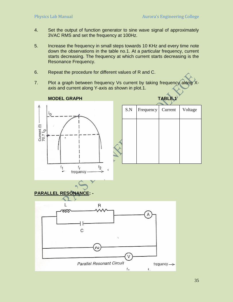
6. L-C-R CIRCUIT. AIM: - To design LCR resonant circuit and plot the resonance circuit of L, C and R components when connected in series and parallel. APPARATUS: Capacitor,resistor,voltmeter,ammeter,frequency,generator,inductor,connecting wires PRINCIPLE: - If the value of the frequency of applied signal is so adjusted that the impedance of the circuit becomes minimum. The current flowing through the circuit will be maximum. This particular frequency at which the impedance of the circuit becomes minimum and therefore the current becomes maximum is called the resonant frequency. SERIES RESONANCE: -
PROCEDURE: - 1. Connect the circuit as shown in figure. Connect resistance R, capacitor C
and inductor L in the circuit. 2. Connect function generator across input of the circuit as shown in figure. 3. Switch ON the function generator using ON/OFF switch provided on the
front panel.
Physics Lab Manual Aurora’s Engineering College
35
4. Set the output of function generator to sine wave signal of approximately 3VAC RMS and set the frequency at 100Hz.
5. Increase the frequency in small steps towards 10 KHz and every time note
down the observations in the table no.1. At a particular frequency, current starts decreasing. The frequency at which current starts decreasing is the Resonance Frequency.
6. Repeat the procedure for different values of R and C. 7. Plot a graph between frequency Vs current by taking frequency along X-
axis and current along Y-axis as shown in plot.1.
MODEL GRAPH TABLE.1
PARALLEL RESONANCE: -
S.N Frequency Current Voltage
Physics Lab Manual Aurora’s Engineering College
36
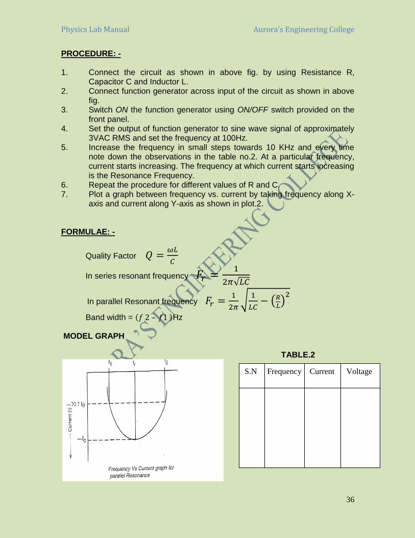
PROCEDURE: - 1. Connect the circuit as shown in above fig. by using Resistance R,
Capacitor C and Inductor L. 2. Connect function generator across input of the circuit as shown in above
fig. 3. Switch ON the function generator using ON/OFF switch provided on the
front panel. 4. Set the output of function generator to sine wave signal of approximately
3VAC RMS and set the frequency at 100Hz. 5. Increase the frequency in small steps towards 10 KHz and every time
note down the observations in the table no.2. At a particular frequency, current starts increasing. The frequency at which current starts increasing is the Resonance Frequency.
6. Repeat the procedure for different values of R and C. 7. Plot a graph between frequency vs. current by taking frequency along X-
axis and current along Y-axis as shown in plot.2. FORMULAE: -
Quality Factor 𝑄 =𝜔𝐿
𝐶
In series resonant frequency 𝐹𝑟 =1
2𝜋√𝐿𝐶
In parallel Resonant frequency 𝐹𝑟 =1
2𝜋√
1
𝐿𝐶− (𝑅
𝐿)
2
Band width = (𝑓 2 – 𝑓1 )Hz
MODEL GRAPH TABLE.2
S.N Frequency Current Voltage

Physics Lab Manual Aurora’s Engineering College
37
OBSERVATIONS: - Series resonant circuit
Capacitance (C) = ……. Resistance (R) =…….. Inductance (I) = …….
Frequency Current Frequency Current
Parallel resonant circuit
Capacitance (C) = …….

Physics Lab Manual Aurora’s Engineering College
38
Resistance (R) =…….. Inductance (I) = ……
Frequency Current Frequency Current
Physics Lab Manual Aurora’s Engineering College
39
CALCULATIONS:- 1. Calculation from the graph(series resonant circuit) a. Resonant frequency fr =
b. Band width ∆𝑓 = |𝑓1 − 𝑓2|
c. Quality factor 𝑄 = 𝑓𝑟
|𝑓1−𝑓2|
d. Resonant frequency 𝐹𝑟 =1
2𝜋√𝐿𝐶
2. Calculation from the graph (parallel resonant circuit) a. Resonant frequency fr =
b. Band width ∆𝑓 = |𝑓1 − 𝑓2|
c. Quality factor 𝑄 = 𝑓𝑟
|𝑓1−𝑓2|
d. Resonant frequency 𝐹𝑟 =1
2𝜋√
1
𝐿𝐶− (𝑅
𝐿)
2
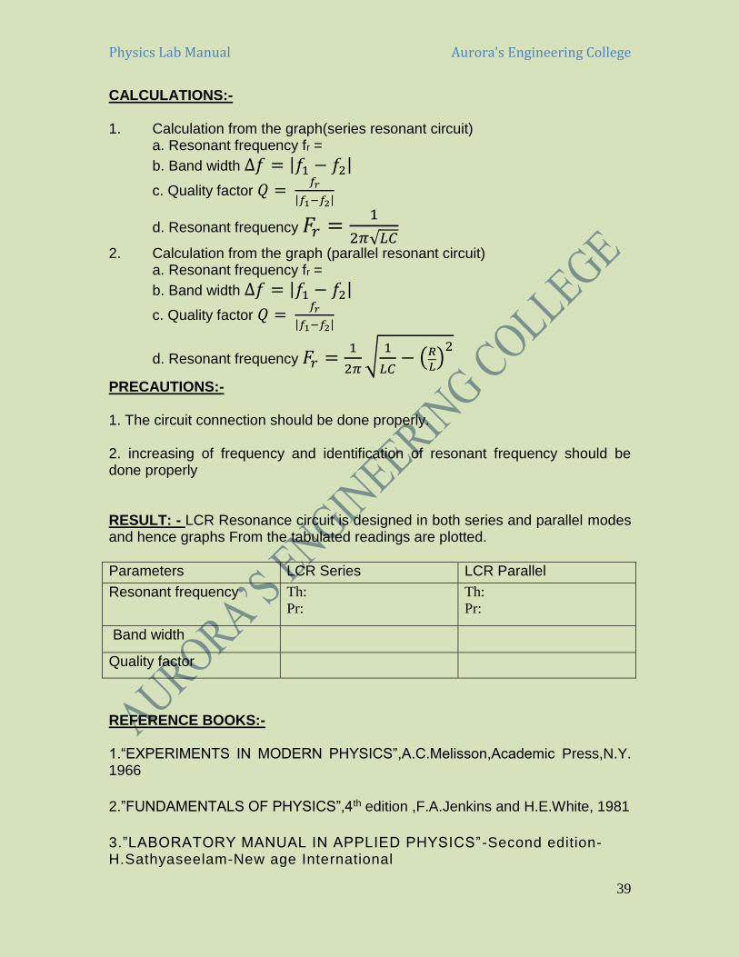
PRECAUTIONS:- 1. The circuit connection should be done properly. 2. increasing of frequency and identification of resonant frequency should be done properly RESULT: - LCR Resonance circuit is designed in both series and parallel modes and hence graphs From the tabulated readings are plotted.
Parameters LCR Series LCR Parallel
Resonant frequency
Th:
Pr:
Th:
Pr:
Band width
Quality factor
REFERENCE BOOKS:- 1.“EXPERIMENTS IN MODERN PHYSICS”,A.C.Melisson,Academic Press,N.Y. 1966
2.”FUNDAMENTALS OF PHYSICS”,4th edition ,F.A.Jenkins and H.E.White, 1981
3.”LABORATORY MANUAL IN APPLIED PHYSICS” -Second edition-H.Sathyaseelam-New age International

Physics Lab Manual Aurora’s Engineering College
40

Physics Lab Manual Aurora’s Engineering College
41

Physics Lab Manual Aurora’s Engineering College
42
7. MAGNETIC FIELD ALONG THE AXIS OF CURRENT CARRYING COIL – STEWART AND GEES METHOD.
AIM: - To study variation of magnetic field with distance on the axis of a circular coil carrying current APPARATUS: - Stewart Gee type galvanometer, battery plug key, commutator, rheostat and ammeter.
Physics Lab Manual Aurora’s Engineering College
43
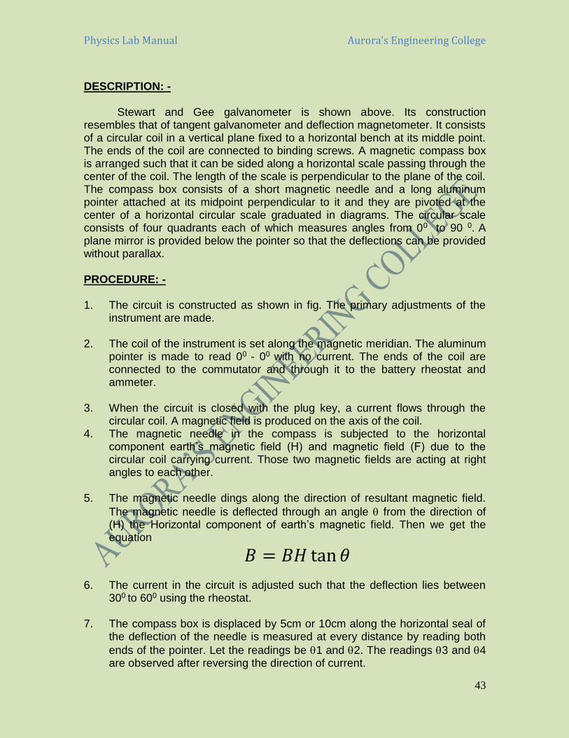
DESCRIPTION: - Stewart and Gee galvanometer is shown above. Its construction resembles that of tangent galvanometer and deflection magnetometer. It consists of a circular coil in a vertical plane fixed to a horizontal bench at its middle point. The ends of the coil are connected to binding screws. A magnetic compass box is arranged such that it can be sided along a horizontal scale passing through the center of the coil. The length of the scale is perpendicular to the plane of the coil. The compass box consists of a short magnetic needle and a long aluminum pointer attached at its midpoint perpendicular to it and they are pivoted at the center of a horizontal circular scale graduated in diagrams. The circular scale consists of four quadrants each of which measures angles from 00 to 90 0. A plane mirror is provided below the pointer so that the deflections can be provided without parallax. PROCEDURE: - 1. The circuit is constructed as shown in fig. The primary adjustments of the
instrument are made. 2. The coil of the instrument is set along the magnetic meridian. The aluminum
pointer is made to read 00 - 00 with no current. The ends of the coil are connected to the commutator and through it to the battery rheostat and ammeter.
3. When the circuit is closed with the plug key, a current flows through the
circular coil. A magnetic field is produced on the axis of the coil. 4. The magnetic needle in the compass is subjected to the horizontal
component earth’s magnetic field (H) and magnetic field (F) due to the circular coil carrying current. Those two magnetic fields are acting at right angles to each other.
5. The magnetic needle dings along the direction of resultant magnetic field.
The magnetic needle is deflected through an angle from the direction of (H) the Horizontal component of earth’s magnetic field. Then we get the equation
𝐵 = 𝐵𝐻 tan 𝜃 6. The current in the circuit is adjusted such that the deflection lies between
300 to 600 using the rheostat. 7. The compass box is displaced by 5cm or 10cm along the horizontal seal of
the deflection of the needle is measured at every distance by reading both
ends of the pointer. Let the readings be 1 and 2. The readings 3 and 4 are observed after reversing the direction of current.

Physics Lab Manual Aurora’s Engineering College
44
8. The experiment is repeated for points on the other side of the coil. If is the
average of the four deflection readings tan B.
9. A graph is drawn with tan along x-axis. This graph shows the variation of magnetic field on the axis of circular coil with distance. It is symmetrical about y-axis and the magnetic field is maximum at the center of the coil.
FORMULA: - The magnetic field B at a point on the axis of a circular coil of a turns and radius a is given by the equation
𝐵 =𝜇0𝑛𝑖𝑎2
2(𝑥2 + 𝑎2)3
2⁄
Where I = current passing through the coil
X = distance of the point from the center of the coil.
OBSERVATIONS: - BH = 0.38x10⁻⁴ Tesla µ0 = 4πX107
Current I = ------ amp. n = …..
S.N
Position magneto main
Distance x
Deflection Average
Tan
B = BH tan
B=
1 2 3 4
Left (-) West of the coil
Right (+) East of the coil
Physics Lab Manual Aurora’s Engineering College
45
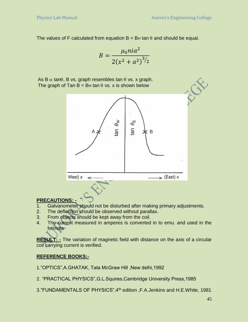
The values of F calculated from equation B = BH tan and should be equal.
𝐵 =𝜇0𝑛𝑖𝑎2
2(𝑥2 + 𝑎2)3
2⁄
As B tan, B vs. graph resembles tan vs. x graph.
The graph of Tan B = BH tan vs. x is shown below
PRECAUTIONS: - 1. Galvanometer should not be disturbed after making primary adjustments. 2. The deflection should be observed without parallax. 3. From objects should be kept away from the coil. 4. The current measured in amperes is converted in to emu. and used in the
formula RESULT: - The variation of magnetic field with distance on the axis of a circular coil carrying current is verified. REFERENCE BOOKS:- 1.”OPTICS”,A.GHATAK, Tata McGraw Hill ,New delhi,1992 2. “PRACTICAL PHYSICS”,G.L.Squires,Cambridge University Press,1985 3.”FUNDAMENTALS OF PHYSICS”,4th edition ,F.A.Jenkins and H.E.White, 1981

Physics Lab Manual Aurora’s Engineering College
46

Physics Lab Manual Aurora’s Engineering College
47
Physics Lab Manual Aurora’s Engineering College
48
8. STUDY THE CHARACTERISTICS OF LED AND LASER SOURCES.
AIM: - To study V-I characteristics of LED and laser diode APPARATUS: - LED and laser trainer kit, digital multimeter, power supply. PRINCIPLE: - The light emitting diode (LED) and Laser diode are popular electronic devices which work on the principle of electroluminescence. Characteristics of LED and LASER diodes: PROCEDURE:-
V-I characteristics of LED
1) Switch on the power supply. 2) Adjust the set P0 Knob to extreme anti clock position to give minimum
output power and observe the power in the power meter. 3) Slowly turn set Po knob clockwise a little and then note load voltage (VL)
across the LED, output terminal also note the readings in ammeter IL. 4) Repeat step 3 for noting various values of voltage and current 5) Plot graph of VL and IL.
Current-Power (I-P) Characteristics of LED and LASER diode The I-P characteristics of laser diode may be well utilized for the determination of quantum efficiency of the light emitting device the differential slope efficiency (dt/dl) is the slope of the L-I characteristics at a particular current. The light emitted by LED is coupled to the power meter through the optical fiber cable. The power received is measured by the digital millimeter. The driving current is supplied using a continuous variable linear regulated DC power supply of 0- 32 volts through a series resistance of 100Ω.
P-I characteristics of LED
1) Adjust the set Po knob to extreme anticlockwise position to give the minimum output in the power meter and observe the output power in the power meter.
2) Slowly turn the set Po knob clockwise a little and then note current (IL) through the LED terminals. Also note the reading in the power meter (Po).
3) Repeat step 2 for noting various values of IL and Po. 4) Plot a graph between IL and Po take closer reading to plot a fine graph.
Physics Lab Manual Aurora’s Engineering College
49
To study the I-P characteristics of LASER :- The above procedure can be followed with change to laser to study the I-P characteristics of laser. OBSERVATIONS:- V-I characteristics of LED
S.NO. Voltage (V) Current (I) mA
I-P characteristics of LED
S.NO. Current (I) mA Optical power (mW)
V-I characteristics of LASER
S.NO. Voltage (V) Current (I) mA
Physics Lab Manual Aurora’s Engineering College
50
I-P characteristics of LASER
S.NO. Current (I) mA Optical power mW
PRECAUTIONS:- 1. Adjusting of knob should be done properly. 2. Increasing of voltage to LED and laser diode should be done gradually. RESULT:- The laser and LED characteristics are observed with different current, voltage and power readings and the graphs are drawn. REFERENCE BOOKS:- 1.”BASIC ELECTRONIC INSTRUMENT” Hand Book ,C.F.Coombs,McGraw-Hill ,1972 2.EXPERIMENTS IN MODERN PHYSICS”,A.C.Melisson,Academic Press,N.Y. 1966 3.“RELIABLE KNOWELDGE”,J.Ziman, Cambridge university Press,Cambridge,1978 4.”LABORATORY MANUAL IN APPLIED PHYSICS” -Second edition-H.Sathyaseelam-New age International

Physics Lab Manual Aurora’s Engineering College
51

Physics Lab Manual Aurora’s Engineering College
52
Physics Lab Manual Aurora’s Engineering College
53
9. STUDY THE CHARACTERISTICS OF P-I-N AND AVALANCHE PHOTODIODE DETECTORS.
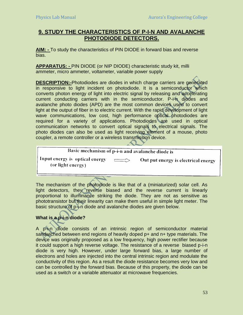
AIM: - To study the characteristics of PIN DIODE in forward bias and reverse bias. APPARATUS: - PIN DIODE (or NIP DIODE) characteristic study kit, milli ammeter, micro ammeter, voltameter, variable power supply DESCRIPTION:-Photodiodes are diodes in which charge carriers are generated in responsive to light incident on photodiode. It is a semiconductor which converts photon energy of light into electric signal by releasing and accelerating current conducting carriers with in the semiconductor. P-i-n diodes and avalanche photo diodes (APD) are the most common devices used to convert light at the output of fiber in to electric current. With the rapid development of light wave communications, low cost, high performance optical photodiodes are required for a variety of applications. Photodiodes are used in optical communication networks to convert optical signals to electrical signals. The photo diodes can also be used as light receiving element of a mouse, photo coupler, a remote controller or a wireless transmission device.
The mechanism of the photodiode is like that of a (miniaturized) solar cell. As light detectors, they reverse biased and the reverse current is linearly proportional to illuminance striking the diode. They are not as sensitive as phototransistor but their linearity can make them useful in simple light meter. The basic structure of p-i-n diode and avalanche diodes are given below. What is a p-i-n diode? A p-i-n diode consists of an intrinsic region of semiconductor material sandwiched between end regions of heavily doped p+ and n+ type materials. The device was originally proposed as a low frequency, high power rectifier because it could support a high reverse voltage. The resistance of a reverse biased p-i-n diode is very high. However, under large forward bias, a large number of electrons and holes are injected into the central intrinsic region and modulate the conductivity of this region. As a result the diode resistance becomes very low and can be controlled by the forward bias. Because of this property, the diode can be used as a switch or a variable attenuator at microwave frequencies.

Physics Lab Manual Aurora’s Engineering College
54
What is an avalanche diode? The avalanche photodiode has a number of different characteristics when compared to the normal p-n, p-i-n photo diodes, making them more suitable for use in some other applications. The main advantages of avalanche diode is greater level of sensitivity. The structure is more complicated than that of the p-i-n device. There are n+, p, un-doped and p+ regions. Light absorption takes place in un-doped region. The avalanche region occurs between the n+ and p-regions. Light enters the un-doped region of the avalanche photodiode and caused the generation of electron-hole pairs. Under the influence of the electric field the electron migrate towards the avalanche region. The electric field causes their velocity to increase to the extent that collisions with the crystal lattice create further electron-hole pairs. In turn these electrons may collide with the crystal lattice to create even more number of electron-hole pairs. In this way a single electron created by light in un-doped region is responsible for the creation of more number of electrons.

Physics Lab Manual Aurora’s Engineering College
55
What are the differences between p-i-n diode and avalanche diode? The avalanche photodiode has a number of differences with when compared to the p-i-n diode. The avalanche process means that a single electron produced by light in the un-doped region in multiplied several times by the avalanche process. As a result the avalanche diode far more sensitive when compared to p-i-n diode. In avalanche process the signal is more noisier compared to the p-i-n diode. N-type guard type ring is also required around the p-n junction to minimize the electric field around the edge of the junction. In avalanche diode the current gain is dependent not only on the bias applied, but also thermal fluctuations.
The Photo diode are characterized by quantum efficiency, responsivety, gain, dark current etc, they are briefly described below Quantum efficiency: - It is defined as the fraction on incident photons having sufficient energy to liberate electrons. It depends both on the wavelength of the incident light and the photo diode material. Responsivity: - It is a practical measure of output current for a given optical power input. It is defined as average output current divided by average incident optical power. Its units are A/W. Dark current: - In the absence of light a small dark current flows in a photo diode which is caused due to leakage in the reverse bias. It is very small and it can be ignored. Photo detectors are used in various different applications, such as radiation detection, smoke detection, and flame detection. They are also used in switching the street lights “on” or “off”, depending on the surrounding light.

Physics Lab Manual Aurora’s Engineering College
56
PROCEDURE: -
1. To study the forward biased characteristics of PIN DIODE:
i. Connect the circuit as shown in fig.1 ii. Using variable power supply set LED current (IL) to about 5mA iii. Using the variable power supply of pin diode, slowly increase the
forward. Voltage (VF) and note the forward current (IF) for various values of (VF) Note the readings in Table – 1.
iv. Repeat the above steps by increasing LED. Current in steps of 5mA.
v. Plot graph for VF Vs IF as shown in fig.
Physics Lab Manual Aurora’s Engineering College
57
2. To study the reverse biased characteristics of Pin diode:
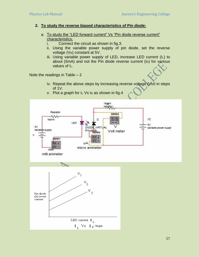
a. To study the “LED forward current” Vs “Pin diode reverse current” characteristics: i. Connect the circuit as shown in fig.3. ii. Using the variable power supply of pin diode, set the reverse
voltage (VR) constant at 5V. iii. Using variable power supply of LED, increase LED current (IL) to
about (5mA) and not the Pin diode reverse current (IR) for various values of IL.
Note the readings in Table – 2
iv. Repeat the above steps by increasing reverse voltage (VR0 in steps of 1V.
v. Plot a graph for IL Vs IR as shown in fig.4
Physics Lab Manual Aurora’s Engineering College
58
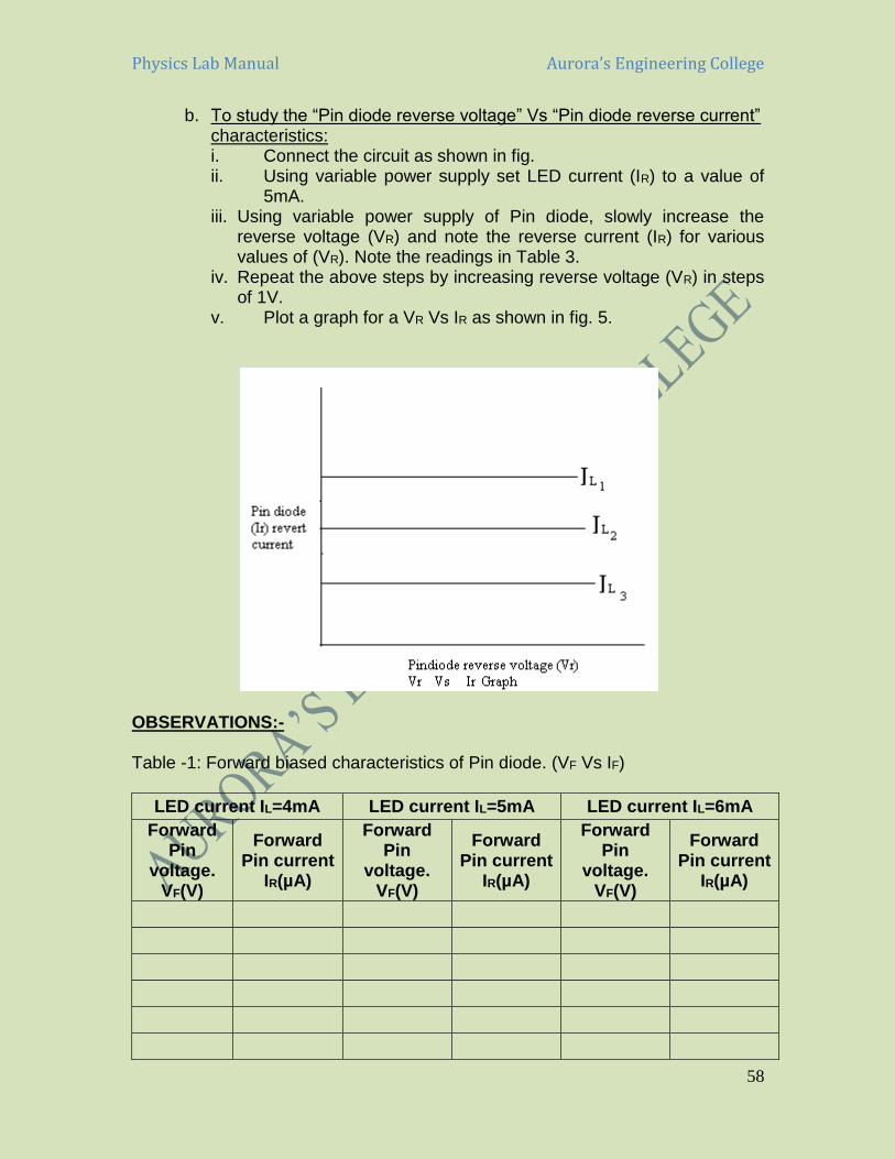
b. To study the “Pin diode reverse voltage” Vs “Pin diode reverse current” characteristics: i. Connect the circuit as shown in fig. ii. Using variable power supply set LED current (IR) to a value of
5mA. iii. Using variable power supply of Pin diode, slowly increase the
reverse voltage (VR) and note the reverse current (IR) for various values of (VR). Note the readings in Table 3.
iv. Repeat the above steps by increasing reverse voltage (VR) in steps of 1V.
v. Plot a graph for a VR Vs IR as shown in fig. 5.
OBSERVATIONS:- Table -1: Forward biased characteristics of Pin diode. (VF Vs IF)
LED current IL=4mA LED current IL=5mA LED current IL=6mA
Forward Pin
voltage. VF(V)
Forward Pin current
IR(µA)
Forward Pin
voltage. VF(V)
Forward Pin current
IR(µA)
Forward Pin
voltage. VF(V)
Forward Pin current
IR(µA)

Physics Lab Manual Aurora’s Engineering College
59
Table-2: Reverse biased characteristics of pin diode (VR Vs IR)
LED current IL=4mA LED current IL=5mA LED current IL=6mA
Reverse Pin
voltage. VR(V)
Reverse Pin current
IR≠µA
Reverse Pin current
VRIV)
Reverse Pin current
(IR(µA)
Reverse Pin
Voltage (VR(V)
Reverse Pin current
(IR≠µA)
Table – 3: Reverse biased pin diode characteristics. LED current Vs PIN reverse current (IL Vs IR)
Reverse Voltage VR = I V
Reverse voltage VR=2v
Reverse voltage VR 3V
PRECAUTIONS:- 1. Biasing should be done properly. 2. Connections should be made carefully. 3. No external light should be incident on photo diode.

Physics Lab Manual Aurora’s Engineering College
60
RESULT: -
Hence, by the above graphs the forward and reverse biased characteristics are verified.
REFERENCE BOOKS:-
1.”VIBRATIONS AND WAVES”,A.P.French,Arnold-Heinemann,New Delhi,1972 2.”BASIC ELECTRONIC INSTRUMENT” Hand Book ,C.F.Coombs,McGraw-Hill ,1972 3.”LABORATORY MANUAL IN APPLIED PHYSICS” -Second edition-H.Sathyaseelam-New age International

Physics Lab Manual Aurora’s Engineering College
61

Physics Lab Manual Aurora’s Engineering College
62
Physics Lab Manual Aurora’s Engineering College
63
10. BENDING LOSSES OF FIBRES.
AIM: - To determine the losses in optical fibers in dB due to macro bending of the fiber. APPARATUS: - Step index F.O. Cable of lengths (a) 1 m (b) 2 m (c) 3 m (d) 4 m (e) 5 m; digital multimeter, Adaptors, D.C. power supply, Fiber optic trainer module, mandrel etc. DESCRIPTION: -
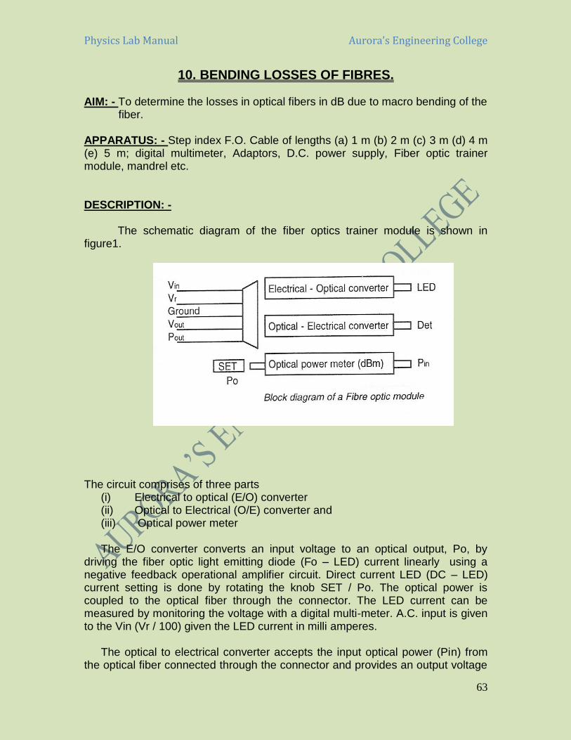
The schematic diagram of the fiber optics trainer module is shown in figure1.
The circuit comprises of three parts
(i) Electrical to optical (E/O) converter (ii) Optical to Electrical (O/E) converter and (iii) Optical power meter
The E/O converter converts an input voltage to an optical output, Po, by
driving the fiber optic light emitting diode (Fo – LED) current linearly using a negative feedback operational amplifier circuit. Direct current LED (DC – LED) current setting is done by rotating the knob SET / Po. The optical power is coupled to the optical fiber through the connector. The LED current can be measured by monitoring the voltage with a digital multi-meter. A.C. input is given to the Vin (Vr / 100) given the LED current in milli amperes.
The optical to electrical converter accepts the input optical power (Pin) from the optical fiber connected through the connector and provides an output voltage

Physics Lab Manual Aurora’s Engineering College
64
(Vo). For D.C. measurements, a multi-meter may be used. For A.C. measurements are made. The optical power meter converts the optical power coupled to it through an SMA terminated optical fiber and facilitates display of the optical power Po in Db. The optical power in dB, is given by the (multi-meter reading / 10) in dB referred to 1 mw.
As in the case of any transmission medium, an optical fiber also suffers from transmission loss as signal propagates through it. Losses in an optical fiber is a result of a number of effects, like fiber to fiber joints, splicing due to axial displacement of fibers, angular displacement of fibers, mismatch of core diameters of fibers, mismatch of N.A.s, improper cleaving and cleaning at the ends of the fibers, macro and micro bending losses, connector losses etc. However, in the present experiment, we confine to the study of the attention in a fiber due to macro bending of the fiber and the adaptors connecting the two fiber patch cords.
If ‘Po’ represents the power launched at the input of a fiber of length ‘L’,
then the power at the output end of the fiber is given by Bouger’s Law. PL = P0 e-αL .............................................................................................................. (1)
Where α is the attenuation coefficient in nepers pre unit length , in practice the attenuation is expressed in dB / km and is defined as
𝛼 = 10 𝑙𝑜𝑔 10 L
P
P
L
0
............................................................ (2)
𝑃𝐿 = 𝑃0 10𝑒
10
L ............................................................ (2)
The typical attenuation coefficient value for a step index fiber used in the experiments is 0.3 dB per meter for light at a wave length of 660 mm. Loss in fibers expressed in decibels is given by:
𝑳𝒐𝒔𝒔 = − 𝟏𝟎
𝑳 𝒍𝒐𝒈
FP
P0 ....................................................... (4)
Where ‘P0’ = Power launched ‘PF’ = Power at the far end of the fiber

Physics Lab Manual Aurora’s Engineering College
65
The loss at each connector junction may vary from 0.3 dB to 0.8 dB. The above two losses are to be determined in the present experiment. PROCEDURE: -
The schematic diagram of the optical fiber loss measurement is shown in figure 2.
One end of the one meter fiber optic cable is connected to the ‘P0’ and the other end is connected to the ‘Pin’ of the loss measurement module. The output power is calibrated in terms of the milli-volts. Hence, the two wires of the power output is connected to the digital multi-meter (DMM). The DMM is set into 2000 mv range. The input of the device is now connected to the A.C. mains. The SET P0 knob is set to a suitable value, say -15 dBm (the DMM is calibrated to read 150 mv). This value is noted as P01.
.
Figure 2: Experimental setup for loss measurement
To determine the bending losses 1) Connect one end of the 1m long optical cable to the output end of the LED
and other end to the Photo detector. 2) Turn the set Po knob clock wise a little. Insert the leads of the dB meter at
the output terminals of the optical power meter circuit and then note the output power (PF1) in the dB meter.
3) Without disturbing the set knob Po wind one turn of optical fiber cable on the mandrel and measure the output power (PF2) in the dB meter, as described above.
4) Repeat the steps 2 and 3 by increasing the set Po knob and measure the corresponding PF1 and PF2 values and note in table1 . the loss due to bending the OFC= PF1-PF2

Physics Lab Manual Aurora’s Engineering College
66
OBSERVATIONS:-
S.No. Output power without bending PF1 dB
Output power with bending PF2 dB
Loss= PF1- PF2
PRECAUTIONS:- 1. Optical fiber cables should be connected appropriately. 2. Power meter values should be increased gradually. RESULT: - The transmission loss in the given optical fiber cable is ………dB.
REFERENCE BOOKS:- 1”.PRACTICAL PHYSICS”,G.L.Squires,Cambridge University Press,1988 2.”FUNDAMENTALS OF PHYSICS”,4th edition ,F.A.Jenkins and H.E.White, 1981 3.”PHYSICS”,M.Alonso and E.J.Finn,Addison Wesley, 1992 4.”LABORATORY MANUAL IN APPLIED PHYSICS” -Second edition-H.Sathyaseelam-New age International

Physics Lab Manual Aurora’s Engineering College
67

Physics Lab Manual Aurora’s Engineering College
68

Physics Lab Manual Aurora’s Engineering College
69
11. Evaluation of numerical aperture of given fiber.
AIM: - To determine the numerical aperture of the given optical fiber. APPARATUS: - One or two meters of a step index optical fiber, digital multimeter, Adaptors, Connectors, D.C. Power supply, Fiber optic trainer module, N.A. measurement jig. DESCRIPTION: - The schematic diagram of the fiber optics trainer module is shown in figure1.
The circuit comprises of three parts (i) Electrical to optical (E/O) converter, (ii) Optical to Electrical (O/E) converter and, (iii) Optical power meter. The E/O converter converts an input voltage to an optical output, P0, by driving the fiber optic light emitting diode (Fo – LED) current linearly using a negative feedback operational amplifier circuit. Direct current LED (DC – LED) current setting is done by rotating the knob SET / PO The optical power is coupled to the optical fiber through the connector. The LED current can be measured by monitoring by voltage with a digital millimeter. A.C. input is given to the Vin (Vr / 100) given the LED current in milliamp. The optical to electrical converter accepts the input optical power (Pin) from the optical fiber connected through the connector and provides an output voltage (Vo). For D.C. measurements, a multi meter may be used. For A.C.

Physics Lab Manual Aurora’s Engineering College
70
measurements an oscilloscope may be used. In the experiment only D.C. measurements are made. The optical power meter converts the optical power coupled to it through an SMA terminated optical fiber and facilitates display of the optical power Po in dB. The optical power in dB, is given by the (multimeter reading/10) in dB referred to 1 mw. The numerical aperture of an optical system is a measure of the light collected by an optical system. It is the product of the refractive index of the incident
Numerical Aperture (𝑁, 𝐴) = 𝑛 𝑖𝑠𝑖𝑛 𝑚𝑎𝑥 For air = 𝑛𝑖 = 1 𝑁. 𝐴. = 𝑠𝑖𝑛 𝑚𝑎𝑥 ………………………………………. .(1) For a step index fiber, the N.A is given by :
𝑁. 𝐴. = 2/122 )( claddingcore nn …………………………………(2)
For small differences in refractive indices between the core and cladding, equation (2) reduces to:
N.A. = 2/1)2( coren …………………………………….….(3)
Where is the fractional differences in the refractive indices of the core and the cladding; i.e.,
core
cladcore
n
nn
Light from the fiber end A falls on the screen BD. Let the diameter of the light falling on the screen = BD = W. Let the distance between the fiber end and the screen = AO = L
Therefore from geometry, BD = W, AO = L , BO = OD = W/2

Physics Lab Manual Aurora’s Engineering College
71
𝐴𝐵 = ( 𝐿 2 + 𝑊2
4 )
12
= [ ( 4 L 2 + W2)1/2 ] / 2
Therefore 𝑁𝐴 =𝑊
√4𝐿2+𝑊2
Knowing the values of W & L the N.A. can be calculated. PROCEDURE: -
The twists or the micro bends on the fiber, if any are to be removed first. In order to remove the twists, the optical fiber is wound on a mandrel. An adhesive tape may be used to hold the windings on the mandrel in the proper position. The experimental set up for the N.A.measurement is shown in figure 2 .
One end of the optical fiber is connected to the N.A. jig through the connector, and the other end of the fiber is connected to the power out Po of the N.A.module . The A.C. mains is switched ON and the light passing through the cable at the other end (coming to the N.A.jig) of the fiber is observed to ensure proper coupling is made or not. The “Set Po” knob is turned in the clock wise direction to get maximum intensity of light through the fiber. The “Set Po” is to be left free at this stage. A screen with concentric circles of known diameter is kept vertically at a distance (L) from the fiber end and the red spot is seen on the screen. The diameter of the red spot can be varied by varying the distance (L)

Physics Lab Manual Aurora’s Engineering College
72
The experiment is repeated for the subsequent diameter of the circles by adjusting the length L. The diameter of the circle is determined using a travelling microscope. For each set of observations, the N.A. is calculated using the equation (4). Using the value of N.A. from (4) in equation (1), the acceptance angle is calculated. The results are tabulated in table1. OBSERVATIONS:-
S NO L (mm) W(mm) 𝑁𝐴 =𝑊
√4𝐿2+𝑊2 𝜽 = 𝐬𝐢𝐧−𝟏 𝑵. 𝑨.
PRECAUTIONS:-
1. Optical fiber cables should be connected appropriately. 2. Power meter values should be increased gradually.
RESULT: - Numerical Aperture of the given optical fiber is ……….
REFERENCE BOOKS:-
1. PRACTICAL PHYSICS”,G.L.Squires,Cambridge University Press,1988 2.”FUNDAMENTALS OF PHYSICS”,4th edition ,F.A.Jenkins and H.E.White, 1981 3.”PHYSICS”, M.Alonso and E.J.Finn, Addison Wesley, 1992 4.”LABORATORY MANUAL IN APPLIED PHYSICS”-Second edition-H.Sathyaseelam-New age International
Physics Lab Manual Aurora’s Engineering College
73

Physics Lab Manual Aurora’s Engineering College
74
Physics Lab Manual Aurora’s Engineering College
75
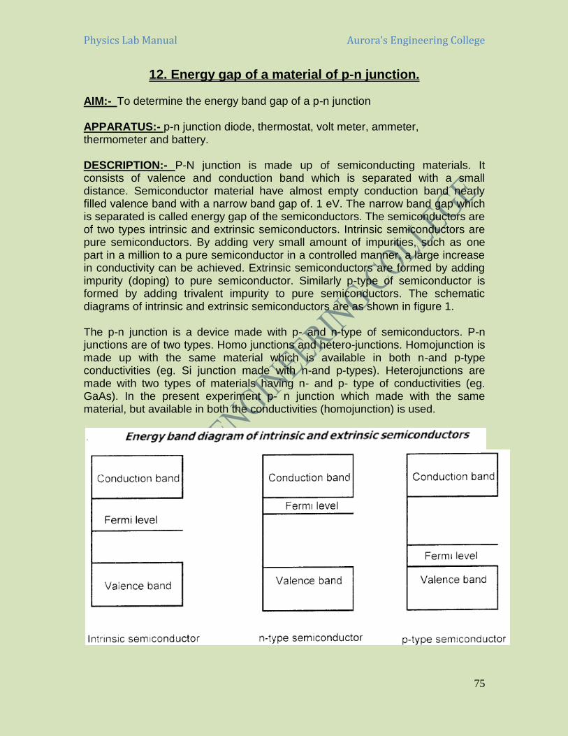
12. Energy gap of a material of p-n junction. AIM:- To determine the energy band gap of a p-n junction APPARATUS:- p-n junction diode, thermostat, volt meter, ammeter, thermometer and battery. DESCRIPTION:- P-N junction is made up of semiconducting materials. It consists of valence and conduction band which is separated with a small distance. Semiconductor material have almost empty conduction band nearly filled valence band with a narrow band gap of. 1 eV. The narrow band gap which is separated is called energy gap of the semiconductors. The semiconductors are of two types intrinsic and extrinsic semiconductors. Intrinsic semiconductors are pure semiconductors. By adding very small amount of impurities, such as one part in a million to a pure semiconductor in a controlled manner, a large increase in conductivity can be achieved. Extrinsic semiconductors are formed by adding impurity (doping) to pure semiconductor. Similarly p-type of semiconductor is formed by adding trivalent impurity to pure semiconductors. The schematic diagrams of intrinsic and extrinsic semiconductors are as shown in figure 1. The p-n junction is a device made with p- and n-type of semiconductors. P-n junctions are of two types. Homo junctions and hetero-junctions. Homojunction is made up with the same material which is available in both n-and p-type conductivities (eg. Si junction made with n-and p-types). Heterojunctions are made with two types of materials having n- and p- type of conductivities (eg. GaAs). In the present experiment p- n junction which made with the same material, but available in both the conductivities (homojunction) is used.

Physics Lab Manual Aurora’s Engineering College
76
The current I through a p-n junction for both signs of applied voltage V I = I0 = [(exp)eV) / (kT0-1] ……………………..(1) Where e = fundamental electronic charge,
K = Boltzmann’s constant, T = Absolute temperature.
For the silicon p-n junctions and positive values of V the exponential term becomes greater than 1. The current through the junction will increase exponentially with V. the dependence on energy gap occurs through the factor I0. I0 is due to the thermal excitation of electrons across the energy gap after which they flow freely across the junction. A complete treatment of the problems that I0 is proportional to the factor f which is given by
kTEgeTf /2/3
Eg = energy gap of the semiconducting material. The I0 can be determined by a simple measurement with a negative bias applied to the junction. However, I0 is so small and careful measurement is necessary. It is essential to generate curves representing equation (1) at several temperatures in order to obtain several values for I0,
PROCEDURE:-
The circuit diagram of the experimental setup for the measurement of energy gap in shown in figure.

Physics Lab Manual Aurora’s Engineering College
77
1. The point contact diode connected in a reverse bias as shown in the
diagram.
2. It is placed in an oil bath and heated uniformly.
3. Saturation current is noted for various temperatures.
4. The bias voltage is maintained at constant value.
5. The readings in the micro-ammeter is noted a function of temperature in
steps of 5 0C.
6. A graph is drawn between with log (1/T) in Kelvin on X-axis and log I0 is on
Y-axis
7. The slope of the graph is calculated and substituted in the formula.
FORMULA:-
Band gap energy eVx
slopekEg 19106.1
2
OBSERVATIONS:-
Temperature (oC)
T (K) 1/T (K-1) I (uA) Ln(I)

Physics Lab Manual Aurora’s Engineering College
78
PRECAUTIONS:-
1. The current flow should not be too high, if the current is high then the
internal heating of the device will occur. This will cause actual temperature
of the junction to be higher then the measured value. This will produce
non-linearity in the curve
2. There may be contact potentials, thermo emfs and meter dc offsets which
must be add and subtract from the readings.
3. Poor contacts result in huge variations in the results and must be carefully
soldered.
4. It is better to repeat a few measurements at end of each run to check the
source of error.
MODEL GRAPH:-
RESULT:-
The energy gap of the p-n junction material is calculated = eV REFERENCE BOOKS: 1.“PRACTICAL PHYSICS”,G.L.Squires,Cambridge University Press,1985 2.“ PHYSICS”,A.C.Melisson,Academic Press,N.Y. 1966 3.“RELIABLE KNOWELDGE”, BY J.Ziman,Cambridgeuniversity press,Cambridge,1978 4.”LABORATORY MANUAL IN APPLIED PHYSICS” -Second edition-H.Sathyaseelam-New age International

Physics Lab Manual Aurora’s Engineering College
79

Physics Lab Manual Aurora’s Engineering College
80
Physics Lab Manual Aurora’s Engineering College
81
13. Torsional pendulum.
AIM: - To determine the rigidity modulus of the material of the given wire by dynamical method using a Torsional pendulum.
APPARATUS: - Torsional Pendulum, Stop Watch, Vertical Pointer, Screw
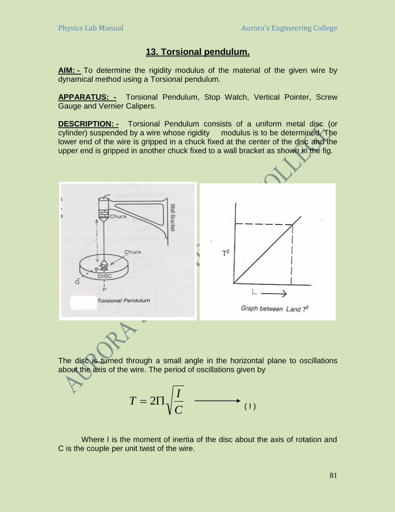
Gauge and Vernier Calipers. DESCRIPTION: - Torsional Pendulum consists of a uniform metal disc (or
cylinder) suspended by a wire whose rigidity modulus is to be determined. The lower end of the wire is gripped in a chuck fixed at the center of the disc and the upper end is gripped in another chuck fixed to a wall bracket as shown in the fig.
The disc is turned through a small angle in the horizontal plane to oscillations about the axis of the wire. The period of oscillations given by
C
IT 2
( I )
Where I is the moment of inertia of the disc about the axis of rotation and C is the couple per unit twist of the wire.

Physics Lab Manual Aurora’s Engineering College
82
But L
nC a
2
4
(II)
Where a is the radius of the wire L is its length and n is the rigidity modulus. From (I) and (II) we have
Ta
LIn
24
8 (III)
In the case of a circular disc (or cylinder) whose geometric axis coincides with axis of rotation of the moment of inertia I is given by
2
2MRI
Where M is the mass of the disc and R is the radius .On substituting the value of I in the Eqn. (III), we get
24
2
2
8
T
LMRn
a
(IV)
PROCEDURE: - A meter wire whose ‘n’ is to be determined is taken without any kinks. The disc is suspended from one end of the wire .The other end of the wire is passed through the chuck fixed to the wall bracket and is rigidly fixed .The length ‘L’ of the wire between the chucks is adjusted to a convenient value (say 50 cms). A pin is fixed vertically on the edge of the disc and a vertical pointer is placed in front of the disc against the pin to serve as a reference to count the oscillations.
The disc is turned in the horizontal plane through a small angle, so as to twist the wire and released. There should not be any up and down and lateral movements of the disc. When it is executing Torsional oscillations, time for 20 oscillations is noted twice and the mean is taken. The period (T) is then calculated 1/T2.
The experiment is repeated for different values of ‘L’ and in each case the period is determined. The value of L/T2 is calculated for each length. The observations are tabulated. From the observations mean the value of L/T 2 is calculated.
The mass ‘M’ of the disc is measured with a physical balance and its
radius ‘R’ is calculated with Vernier calipers. The radius of the wire ‘a’ is determined very accurately with screw gauge at three of four different places and means value is taken since it occurs in fourth power.
Physics Lab Manual Aurora’s Engineering College
83
Substituting these values in eqn (IV) ‘n’ is calculated. A graph is drawn
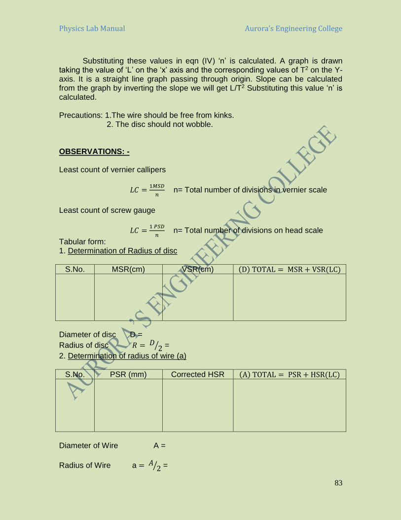
taking the value of ‘L’ on the ‘x’ axis and the corresponding values of T2 on the Y-axis. It is a straight line graph passing through origin. Slope can be calculated from the graph by inverting the slope we will get L/T2 Substituting this value ‘n’ is calculated. Precautions: 1.The wire should be free from kinks. 2. The disc should not wobble. OBSERVATIONS: - Least count of vernier callipers
𝐿𝐶 =1𝑀𝑆𝐷
𝑛 n= Total number of divisions in vernier scale
Least count of screw gauge
𝐿𝐶 =1 𝑃𝑆𝐷
𝑛 n= Total number of divisions on head scale
Tabular form: 1. Determination of Radius of disc
S.No. MSR(cm) VSR(cm) (D) TOTAL = MSR + VSR(LC)
Diameter of disc D =
Radius of disc 𝑅 = 𝐷2⁄ =
2. Determination of radius of wire (a)
S.No. PSR (mm) Corrected HSR (A) TOTAL = PSR + HSR(LC)
Diameter of Wire A =
Radius of Wire a = 𝐴2⁄ =

Physics Lab Manual Aurora’s Engineering College
84
Least count of Vernier callipers(L.C) = ------------------cms Least count of Screw gauge (L.C) = ------------------cms Average radius of the wire (a) = ------------------------cms Mass of the disc (M) = -----------------------------------gms Mean radius of the disc R = ------------------------------cms 3. Table to find time period
S.No Length
L
Time for 20 oscillations Time Period
T=Meantime/20 T2 L/T2
Trail I Trail II Mean time
Mean value of L/T2 = Calculations
𝒏 = (𝟖𝝅
𝟐) (
𝑴𝑹𝟐
𝒂𝟒 ) (𝑳
𝑻𝟐) By table
𝒏 = (𝟖𝝅
𝟐) (
𝑴𝑹𝟐
𝒂𝟒 ) (𝟏
𝑺𝒍𝒐𝒑𝒆) By Graph
PRECAUTIONS:- 1. The disc should be handled carefully. 2. The time for oscillations should be correctly noted. 3. Kinks should not be present along the length of the wire.
Physics Lab Manual Aurora’s Engineering College
85
RESULT: - Rigidity modulus (n) of the wire -----------------dynes/cm2(By table) Rigidity modulus (n) of the wire -----------------dynes/cm2(By graph) REFERENCE BOOKS: 1.”FUNDAMENTALS OF PHYSICS”,D.Halliday,R.Resnick and J.Walkar,John wiley and sons,New York,2001 2.”VIBRATIONS AND WAVES”,A.P.French,Arnold-Heinemann,New Delhi,1972 3.”LABORATORY MANUAL IN APPLIED PHYSICS” -Second edition-H.Sathyaseelam-New age International

Physics Lab Manual Aurora’s Engineering College
86

Physics Lab Manual Aurora’s Engineering College
87

Physics Lab Manual Aurora’s Engineering College
88
14. SINGLE SLIT DIFFRACTION USING LASER.
AIM: - To determine the wavelength of given laser source by plotting diffraction minima’s. APPARATUS:-Track and screen from the Basic Optics System, Laser source, Single Slit Disk, Screen white paper, Graduated Scale. DESCRIPTION:- Since the work of Thomas Young, about 1800, light has been thought of as a wave. One can, therefore, speak of the amplitude and phase of a light wave at any point in space. As like any other wave, two or more light waves may interfere at any point to give either an increase or decrease in wave amplitude at that point. When a light wave encounters an obstacle, the light interacts with the material of the obstacle. As a result, the amplitude and phase of the wave is partly changed. The modified part of the wave may then interfere with the rest of the wave, producing a pattern of light and dark. These effects are not usually noticeable because we deal with obstacles large compared to a wavelength, and we do not closely examine the shadows cast by such objects. In that case, a ray picture is quite adequate. If we use a very small obstacle, or look carefully at the shadow, we will see the effects of interference between various parts of the wave. In the laboratory, it is possible to make a small slit. When the obstacle is illuminated by a small light source a screen placed near the slit will show the expected shadow pattern of a bright line on a dark background. As the screen is moved away from the slit, the pattern becomes more complicated, due to the interference of the parts of the wave that interact with the slit edges. At very large distances, one sees an array of bright lines, spaced at regular intervals. Laser light is much more coherent than light from conventional sources. So that one may observe interference effects even when the path difference between the interfering rays is much greater than 109 wavelengths. Figure -1 is schematic of the apparatus used to observe this effect.
Fig. 1. Arrangement for observing diffraction with slit and point source An exact calculation of the diffraction pattern for the situation we have been considering more generally the angle to the maxima (bright fringes) in the interference pattern is given by
Physics Lab Manual Aurora’s Engineering College
89
,.....)3,2,1,0(sin mmd
𝜆 =𝑎 sin 𝜃
𝑚
Where d is the slit separation, λ is the wavelength of the light, and m is the order (0 for the central maximum, 1 for the first side maximum, 2 for the second side maximum,. . . counting from the center out?. Since the angles are usually small, it can be assumed that
tansin
Set Up:-
PROCEDURE:-
1. Set up the laser at one end of the optical bench and place the single slit
disk in its holder (about 3 cm) in front of the laser. Orient the optical bench
so the laser points toward the wall (see figure-3).

Physics Lab Manual Aurora’s Engineering College
90
2. Set up the white screen at the other end of the bench. Cover the screen
with a sheet of white paper.
3. Select the appropriate slit width (about 0.04mm) by rotating the slit disk
until the slit is centered in the slit holder.
4. Adjust the position of the laser beam from left-to-right and up-and-down
until the beam is centered on the slit.
5. To get perfect diffraction pattern adjust the length between source and slit
and to see the pattern clearly this should be performed in the dark room.
6. Determine the distance from the slit to the screen (D). Note that the slit is
not aligned with the center of the holder.
7. With the room lights off, mark of the positions of minima in the diffraction
pattern on the screen(graph sheet). Label the order of the minima m = 1,2,
etc. and also central maxima.
8. Sketch the diffraction pattern in the lab notebook.
9. Remove the single slit carefully and find its width of the slit using travelling
microscope without disturbing the slit width. Let it be ‘a’ cm.
10. Remove the graph paper, using this measure the distances between the
first minima’s and note the half of this values. Let it be ‘r1’ from first minima
where m=1.
11. Again measure the distance between the second minima‘s let it be ‘r2’
from second minima m=2
12. Repeat the procedure for different minima’s.
Physics Lab Manual Aurora’s Engineering College
91
OBSERVATIONS:-
Least count = 1 𝑀𝑆𝐷
𝑁𝑜 𝑑𝑖𝑣 𝑖𝑛 𝑣𝑒𝑟𝑛𝑖𝑒𝑟 𝑠𝑐𝑎𝑙𝑒
To find the slit width of the first slit.
S.NO. M.S.R. V.C. MSR+(LC) VC
S1 = ……………cm
To find the slit width of the second slit.
S.NO. M.S.R. V.C. MSR+(LC) VC
S2 = ………….cm. To determine the wavelength of laser source
Slit width ‘a’ cm
Order of diffraction
(m) ‘r’ cm ‘L’ CM
sin 𝜃
=𝑟
√𝑟2 + 𝑙2
𝜆 =𝑎 sin 𝜃
𝑚
S1
S2
PRECAUTIONS:-
1. Under any circumstance do not look directly into the laser beam.
2. Do not shine the laser toward anyone.

Physics Lab Manual Aurora’s Engineering College
92
3. Adjustment of slit, laser must be made properly so that fringes are bright
and distinct.
4. Since the linear shift d is proportional to D, it should be fairly large (around
1 meter)
5. Make sure that a strong monochromatic source of light is used.
RESULT:- The wavelength of given laser light is …………….. REFERENCE BOOKS:- 1.”THE FEYNMAN LECTURES IN PHYSICS”,R.P.Feynman,R.B. Leighton and M.Sands,Addison Wesley ,1963 2. EXPERIMENTS IN MODERN PHYSICS”,A.C.Melisson,Academic Press,N.Y. 1966 3.”OPTICS”, A.GHATAK, Tata McGraw Hill, New delhi,1992

Physics Lab Manual Aurora’s Engineering College
93
Physics Lab Manual Aurora’s Engineering College
94

Physics Lab Manual Aurora’s Engineering College
95
15. CHARACTERISTICS OF A SOLAR CELL AIM: - To find out the fill factor of given solar cell. APPRATUS: - Solar cell circuit, voltmeter, micro ammeter, digital multimeter. DESCRIPTION:- Fill Factor: Fill factor is the ratio of actual maximum obtainable power (Vm * Im) to the theoretical (not actually obtainable) power.
PROCEDURE:- 1) Connect the circuit as shown in diagram. 2) Switch on the lamp. 3) Use digital multimeter as voltmeter and micro ammeter for measuring current. 4) Measure short circuit current (ISC) for zero load (i.e. RL = 0) 5) Measure open circuit voltage (VOC) when RL is maximum. 6) Now make RL = 0, vary RL and note corresponding values of voltage and current. 7) Plot I-V curve. 8) Draw a line making an angle 450 with X-axis to meet the curve at a Point, find its co-ordinate Im and Vm gives maximum power dissipation. 9) Calculate fill factor ‘FF’.

Physics Lab Manual Aurora’s Engineering College
96
OBSERVATIONS:- Tabular column:
S.NO Voltage Current(µA)
______ISC
______Voc
Model Graph:-
OBSERVATIONS (FROM GRAPH):- 1) Short circuit current Isc = ---------- μA 2) Open circuit voltage Voc = ---------- V 3) Maximum current Im = ---------- μA 4) Maximum voltage Vm = ---------- V
Physics Lab Manual Aurora’s Engineering College
97
CALCULATIONS:-
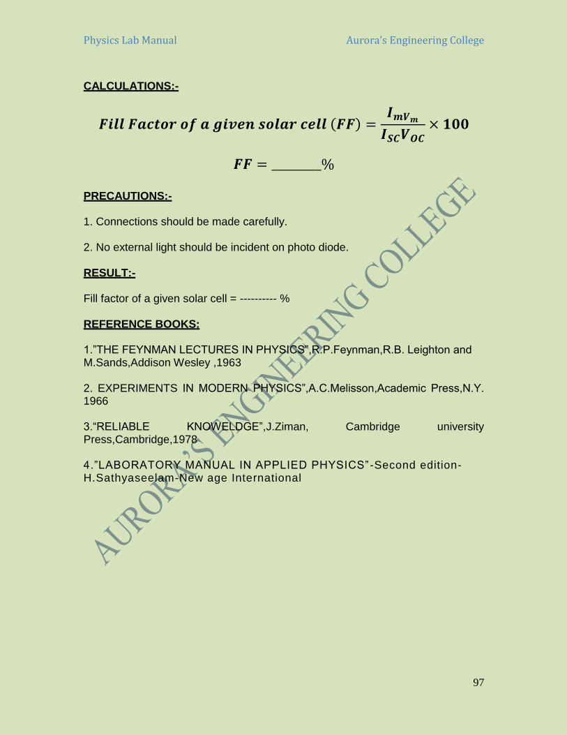
𝑭𝒊𝒍𝒍 𝑭𝒂𝒄𝒕𝒐𝒓 𝒐𝒇 𝒂 𝒈𝒊𝒗𝒆𝒏 𝒔𝒐𝒍𝒂𝒓 𝒄𝒆𝒍𝒍 (𝑭𝑭) =𝑰𝒎𝑽𝒎
𝑰𝑺𝑪𝑽𝑶𝑪× 𝟏𝟎𝟎
𝑭𝑭 = _________% PRECAUTIONS:- 1. Connections should be made carefully. 2. No external light should be incident on photo diode. RESULT:- Fill factor of a given solar cell = ---------- % REFERENCE BOOKS: 1.”THE FEYNMAN LECTURES IN PHYSICS”,R.P.Feynman,R.B. Leighton and M.Sands,Addison Wesley ,1963 2. EXPERIMENTS IN MODERN PHYSICS”,A.C.Melisson,Academic Press,N.Y. 1966 3.“RELIABLE KNOWELDGE”,J.Ziman, Cambridge university Press,Cambridge,1978 4.”LABORATORY MANUAL IN APPLIED PHYSICS” -Second edition-H.Sathyaseelam-New age International

Physics Lab Manual Aurora’s Engineering College
98

Physics Lab Manual Aurora’s Engineering College
99

Physics Lab Manual Aurora’s Engineering College
100