


Languages
Pages
Legal

© Lothar ThieleComputer Engineering and Networks Laboratory
Embedded Systems3. Hardware Software Interface

3 ‐ 2
Do you Remember ?
3 ‐ 3
3 ‐ 4
High‐Level Physical View
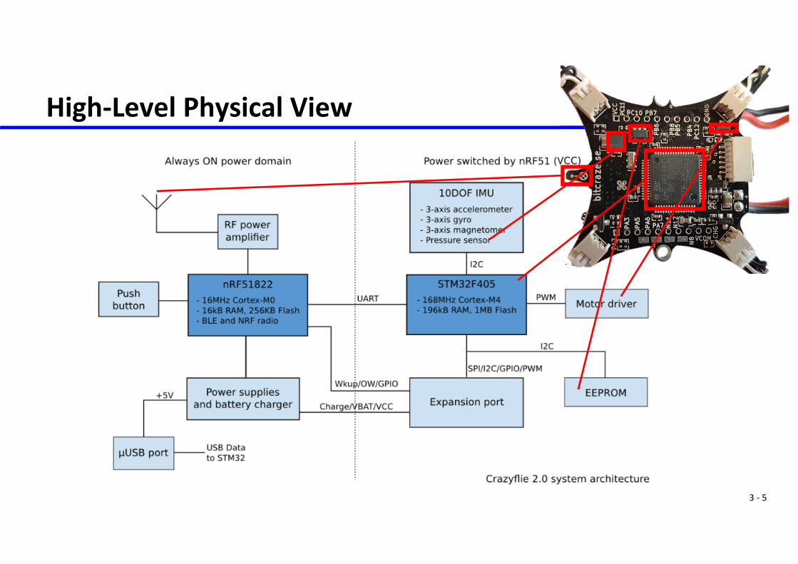
3 ‐ 5
High‐Level Physical View
3 ‐ 6
What you will learn …Hardware‐Software Interfaces in Embedded Systems
Storage SRAM / DRAM / Flash Memory Map
Input and Output UART Protocol Memory Mapped Device Access SPI Protocol
Interrupts Clocks and Timers
Clocks Watchdog Timer System Tick Timer and PWM

3 ‐ 7
Storage
3 ‐ 8
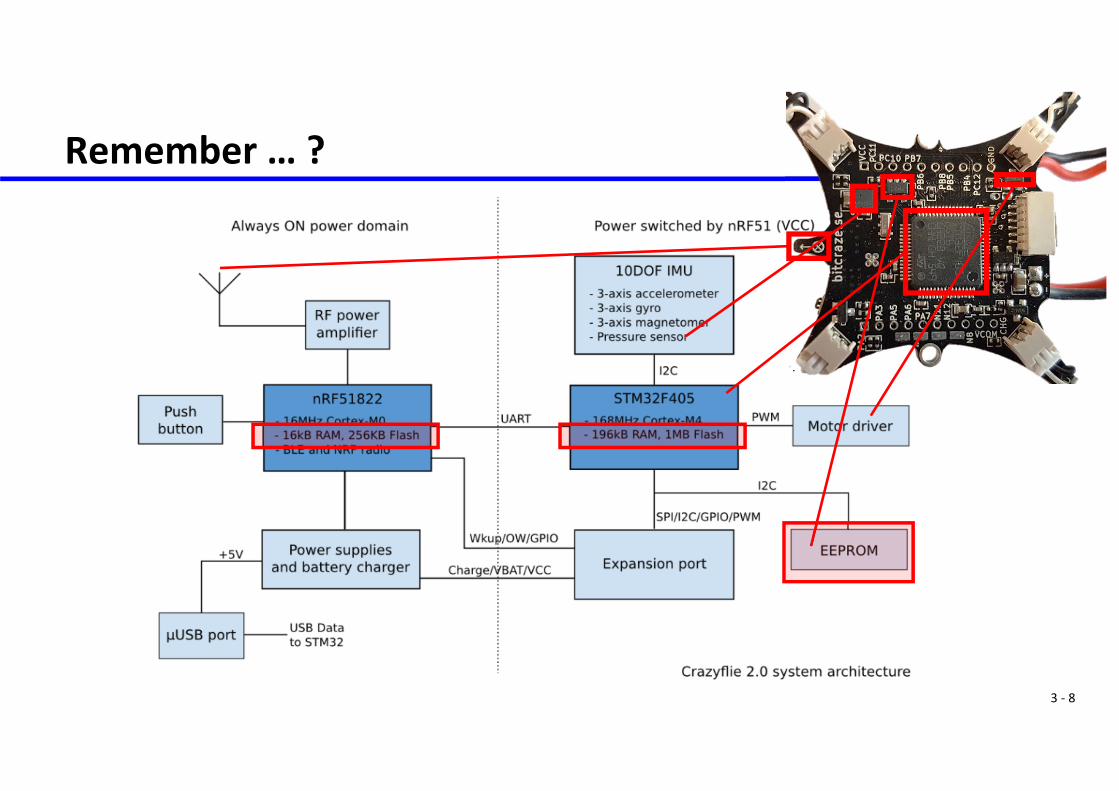
Remember … ?
3 ‐ 9
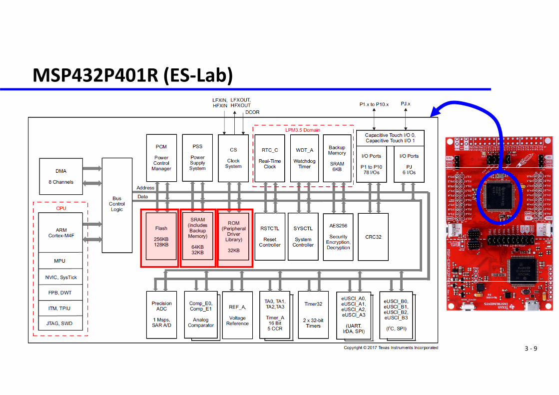
MSP432P401R (ES‐Lab)
3 ‐ 10
StorageSRAM / DRAM / Flash
3 ‐ 11
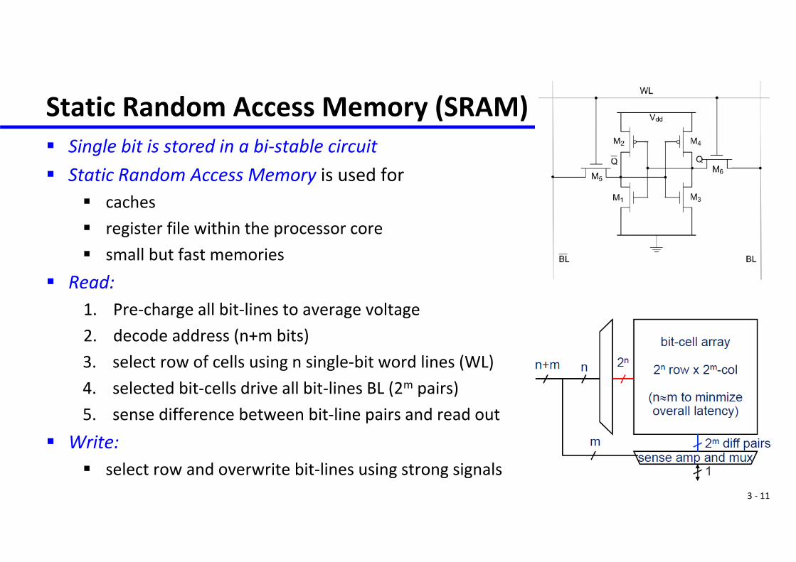
Static Random Access Memory (SRAM) Single bit is stored in a bi‐stable circuit Static Random Access Memory is used for
caches register file within the processor core small but fast memories
Read: 1. Pre‐charge all bit‐lines to average voltage2. decode address (n+m bits)3. select row of cells using n single‐bit word lines (WL) 4. selected bit‐cells drive all bit‐lines BL (2m pairs)5. sense difference between bit‐line pairs and read out
Write: select row and overwrite bit‐lines using strong signals
3 ‐ 12
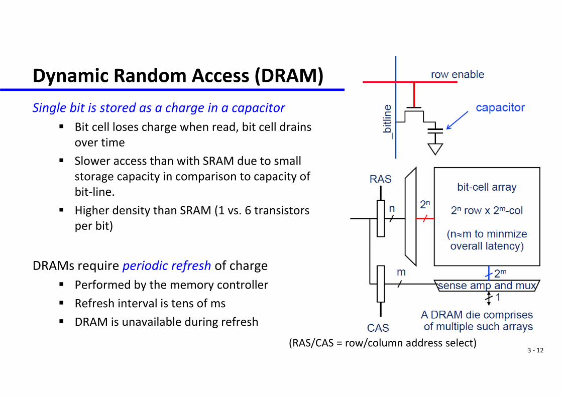
Dynamic Random Access (DRAM)Single bit is stored as a charge in a capacitor
Bit cell loses charge when read, bit cell drains over time
Slower access than with SRAM due to smallstorage capacity in comparison to capacity of bit‐line.
Higher density than SRAM (1 vs. 6 transistors per bit)
DRAMs require periodic refresh of charge Performed by the memory controller Refresh interval is tens of ms DRAM is unavailable during refresh
(RAS/CAS = row/column address select)
3 ‐ 13
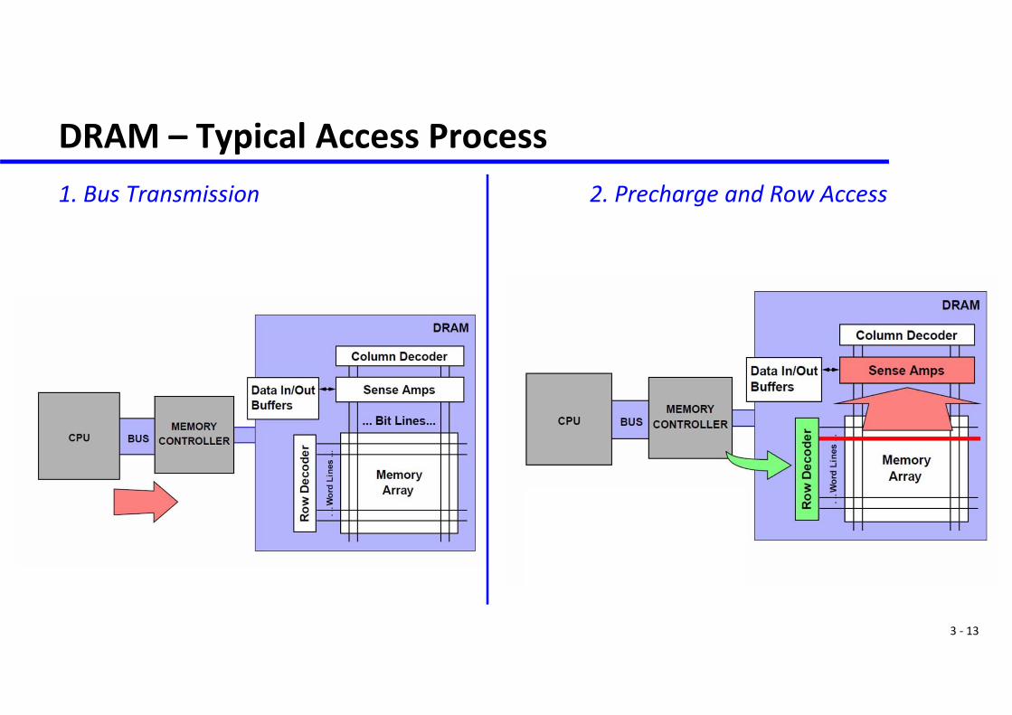
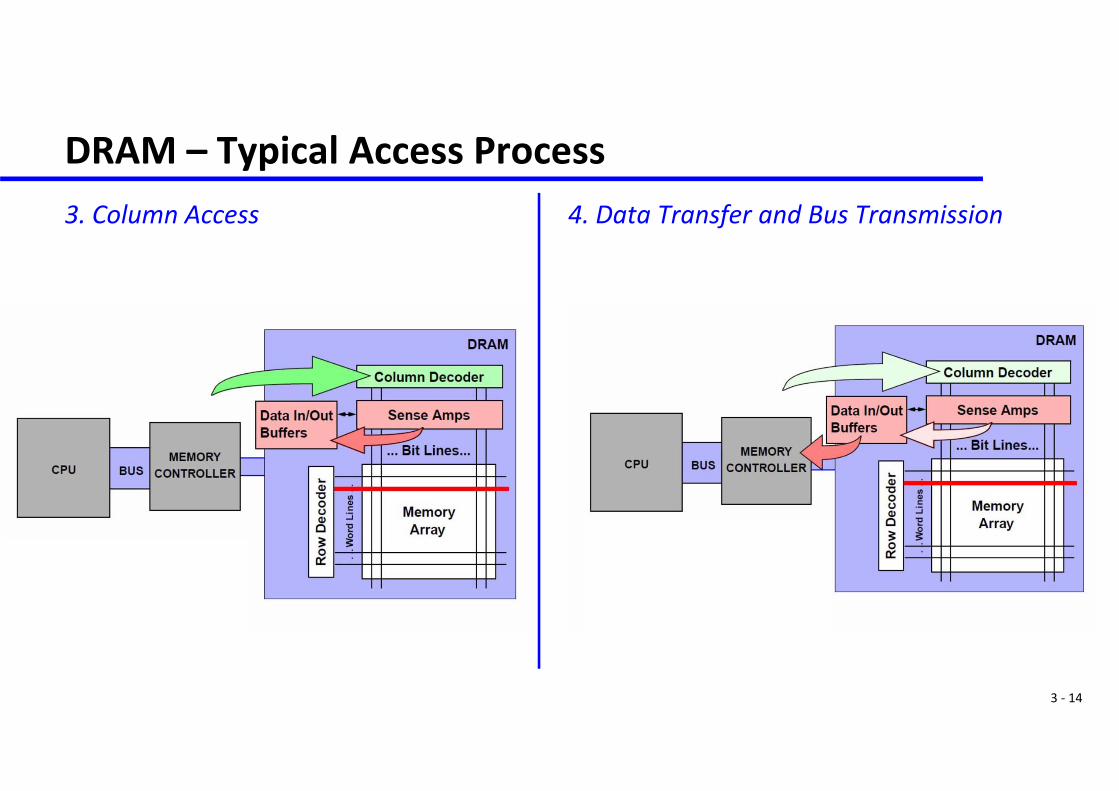
DRAM – Typical Access Process1. Bus Transmission 2. Precharge and Row Access
3 ‐ 14
DRAM – Typical Access Process3. Column Access 4. Data Transfer and Bus Transmission

3 ‐ 15
Flash MemoryElectrically modifiable, non‐volatile storagePrinciple of operation:
Transistor with a second “floating” gate Floating gate can trap electrons This results in a detectable change in
threshold voltage

3 ‐ 16
NAND and NOR Flash Memory
Fast random access
3 ‐ 17
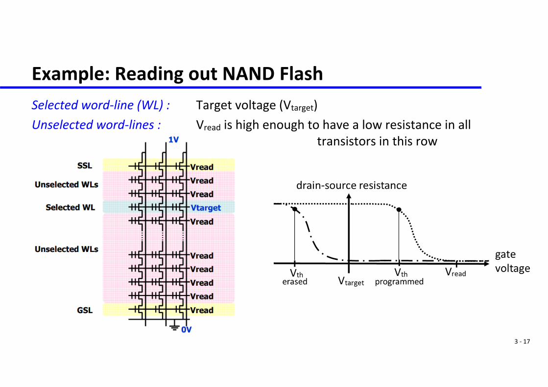
Example: Reading out NAND FlashSelected word‐line (WL) : Target voltage (Vtarget)Unselected word‐lines : Vread is high enough to have a low resistance in all
transistors in this row

3 ‐ 18
StorageMemory Map
3 ‐ 19
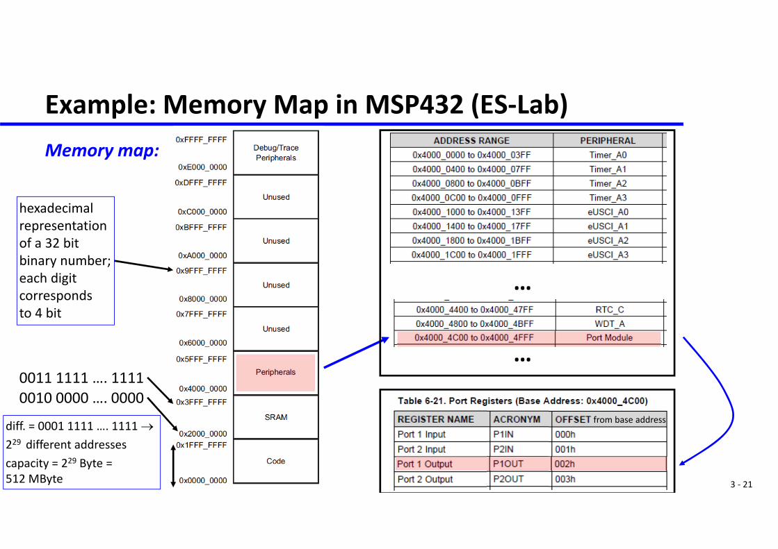
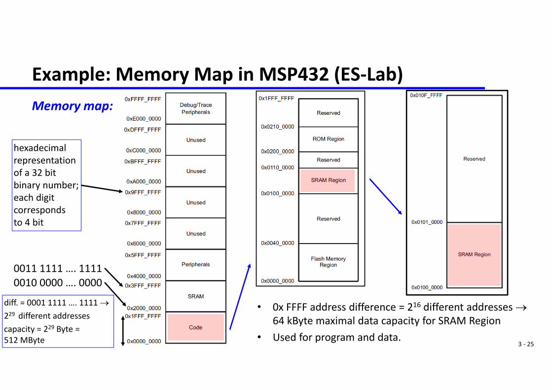
Example: Memory Map in MSP432 (ES‐Lab)Available memory:
The processor used in the lab (MSP432P401R) has built in 256kB flash memory, 64kB SRAM and 32kB ROM (Read Only Memory).
Address space: The processor uses 32 bit addresses. Therefore, the addressable memory space is
4 GByte (= 232 Byte) as each memory location corresponds to 1 Byte. The address space is used to address the memories (reading and writing), to
address the peripheral units, and to have access to debug and trace information (memory mapped microarchitecture).
The address space is partitioned into zones, each one with a dedicated use. The following is a simplified description to introduce the basic concepts.
3 ‐ 20
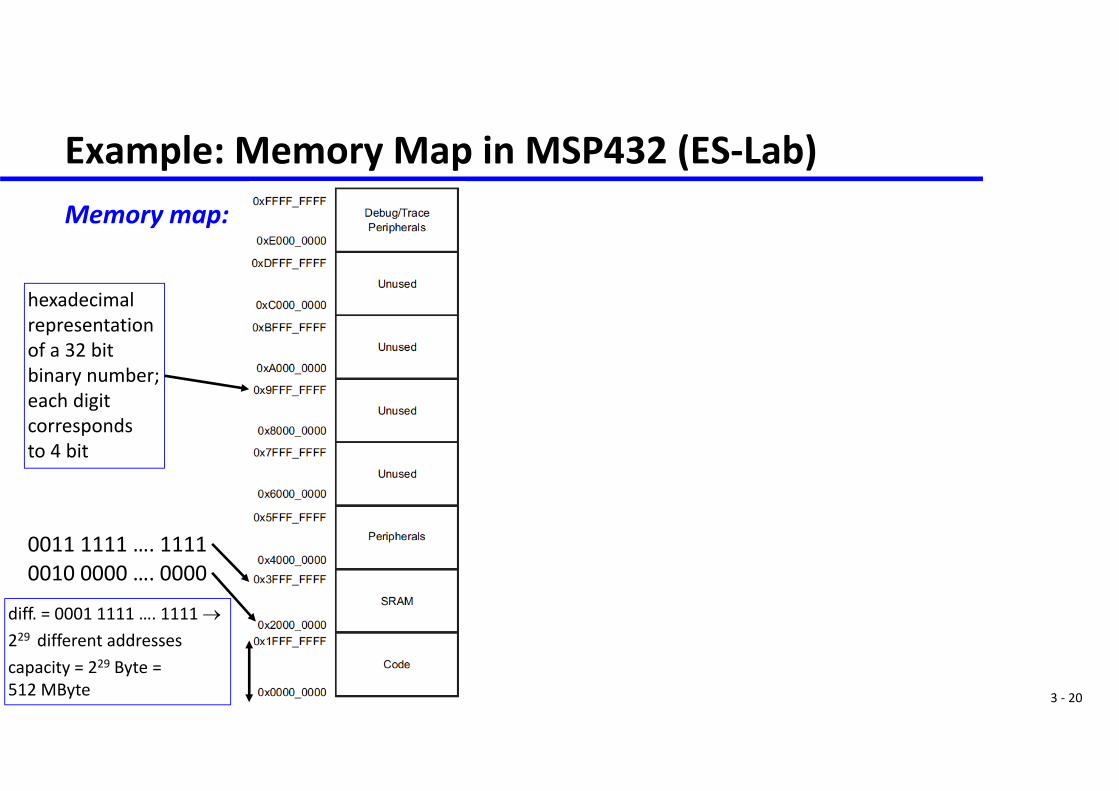
Example: Memory Map in MSP432 (ES‐Lab)Memory map:
hexadecimalrepresentationof a 32 bit binary number;each digit correspondsto 4 bit
0011 1111 …. 11110010 0000 …. 0000
diff. = 0001 1111 …. 1111 229 different addressescapacity = 229 Byte = 512 MByte
3 ‐ 21
Example: Memory Map in MSP432 (ES‐Lab)Memory map:
hexadecimalrepresentationof a 32 bit binary number;each digit correspondsto 4 bit
0011 1111 …. 11110010 0000 …. 0000
…
…
diff. = 0001 1111 …. 1111 229 different addressescapacity = 229 Byte = 512 MByte
from base address
3 ‐ 22
Example: Memory Map in MSP432 (ES‐Lab)Memory map:
hexadecimalrepresentationof a 32 bit binary number;each digit correspondsto 4 bit
0011 1111 …. 11110010 0000 …. 0000
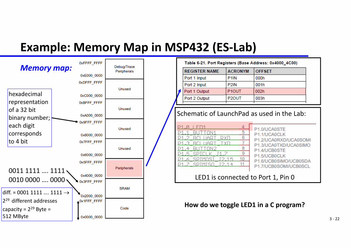
Schematic of LaunchPad as used in the Lab:
LED1 is connected to Port 1, Pin 0
How do we toggle LED1 in a C program?
diff. = 0001 1111 …. 1111 229 different addressescapacity = 229 Byte = 512 MByte
3 ‐ 23
Example: Memory Map in MSP432 (ES‐Lab)Memory map:
hexadecimalrepresentationof a 32 bit binary number;each digit correspondsto 4 bit
0011 1111 …. 11110010 0000 …. 0000
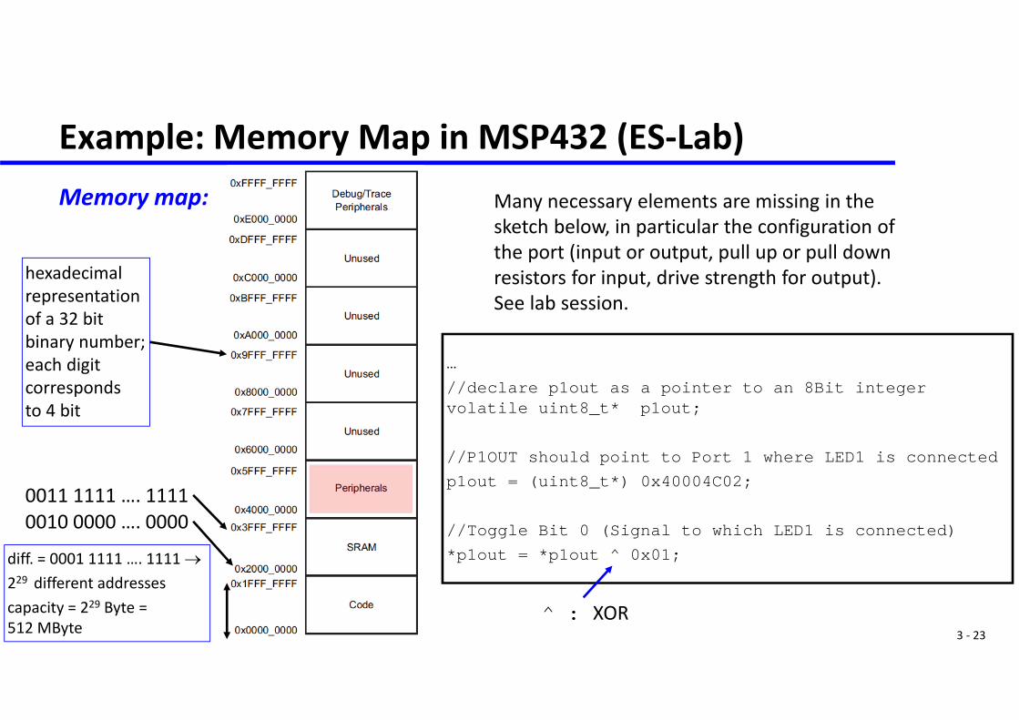
…//declare p1out as a pointer to an 8Bit integer volatile uint8_t* p1out;
//P1OUT should point to Port 1 where LED1 is connectedp1out = (uint8_t*) 0x40004C02;
//Toggle Bit 0 (Signal to which LED1 is connected)*p1out = *p1out ^ 0x01;
Many necessary elements are missing in thesketch below, in particular the configuration ofthe port (input or output, pull up or pull downresistors for input, drive strength for output).See lab session.
diff. = 0001 1111 …. 1111 229 different addressescapacity = 229 Byte = 512 MByte
^ : XOR
3 ‐ 24
Example: Memory Map in MSP432 (ES‐Lab)Memory map:
hexadecimalrepresentationof a 32 bit binary number;each digit correspondsto 4 bit
0011 1111 …. 11110010 0000 …. 0000
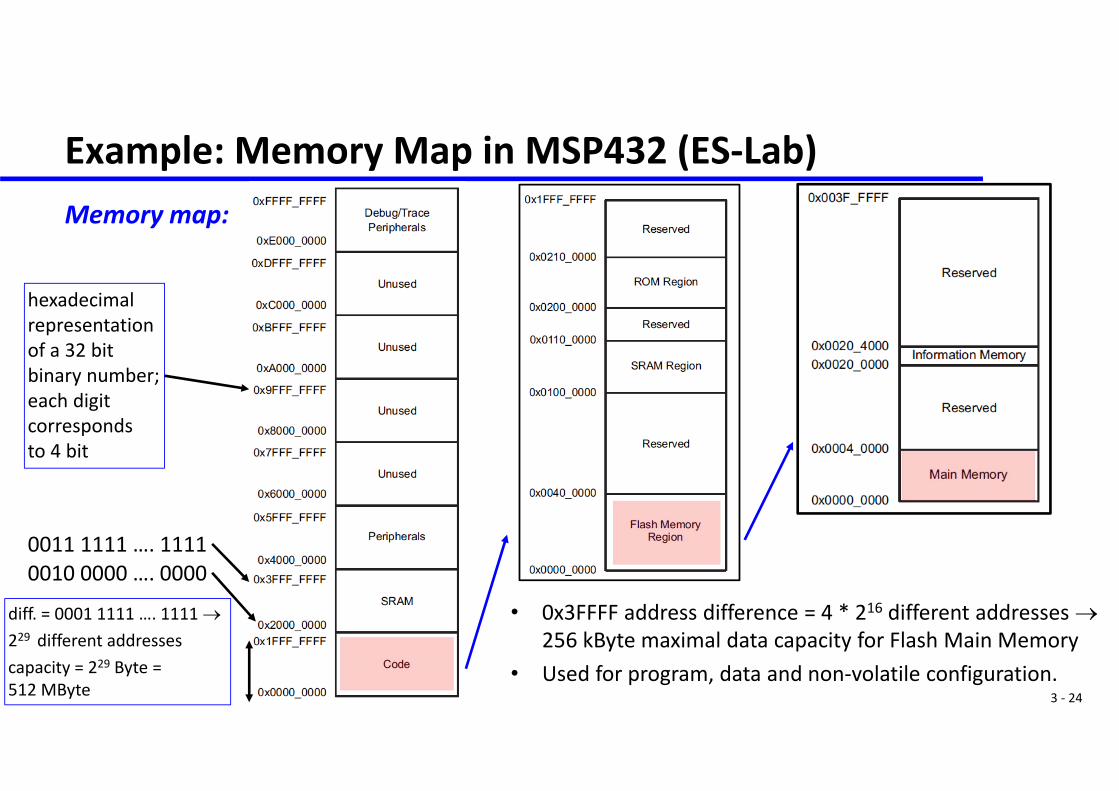
• 0x3FFFF address difference = 4 * 216 different addresses 256 kByte maximal data capacity for Flash Main Memory
• Used for program, data and non‐volatile configuration.
diff. = 0001 1111 …. 1111 229 different addressescapacity = 229 Byte = 512 MByte
3 ‐ 25
Example: Memory Map in MSP432 (ES‐Lab)Memory map:
hexadecimalrepresentationof a 32 bit binary number;each digit correspondsto 4 bit
0011 1111 …. 11110010 0000 …. 0000
• 0x FFFF address difference = 216 different addresses 64 kByte maximal data capacity for SRAM Region
• Used for program and data.
diff. = 0001 1111 …. 1111 229 different addressescapacity = 229 Byte = 512 MByte

3 ‐ 26
Input and Output

3 ‐ 27
Device CommunicationVery often, a processor needs to exchange information with other processors or devices. To satisfy various needs, there exists many different communication protocols, such as
UART (Universal Asynchronous Receiver‐Transmitter) SPI (Serial Peripheral Interface Bus) I2C (Inter‐Integrated Circuit) USB (Universal Serial Bus)
As the principles are similar, we will just explain a representative of an asynchronous protocol (UART, no shared clock signal between sender and receiver) and one of a synchronous protocol (SPI , shared clock signal).
3 ‐ 28
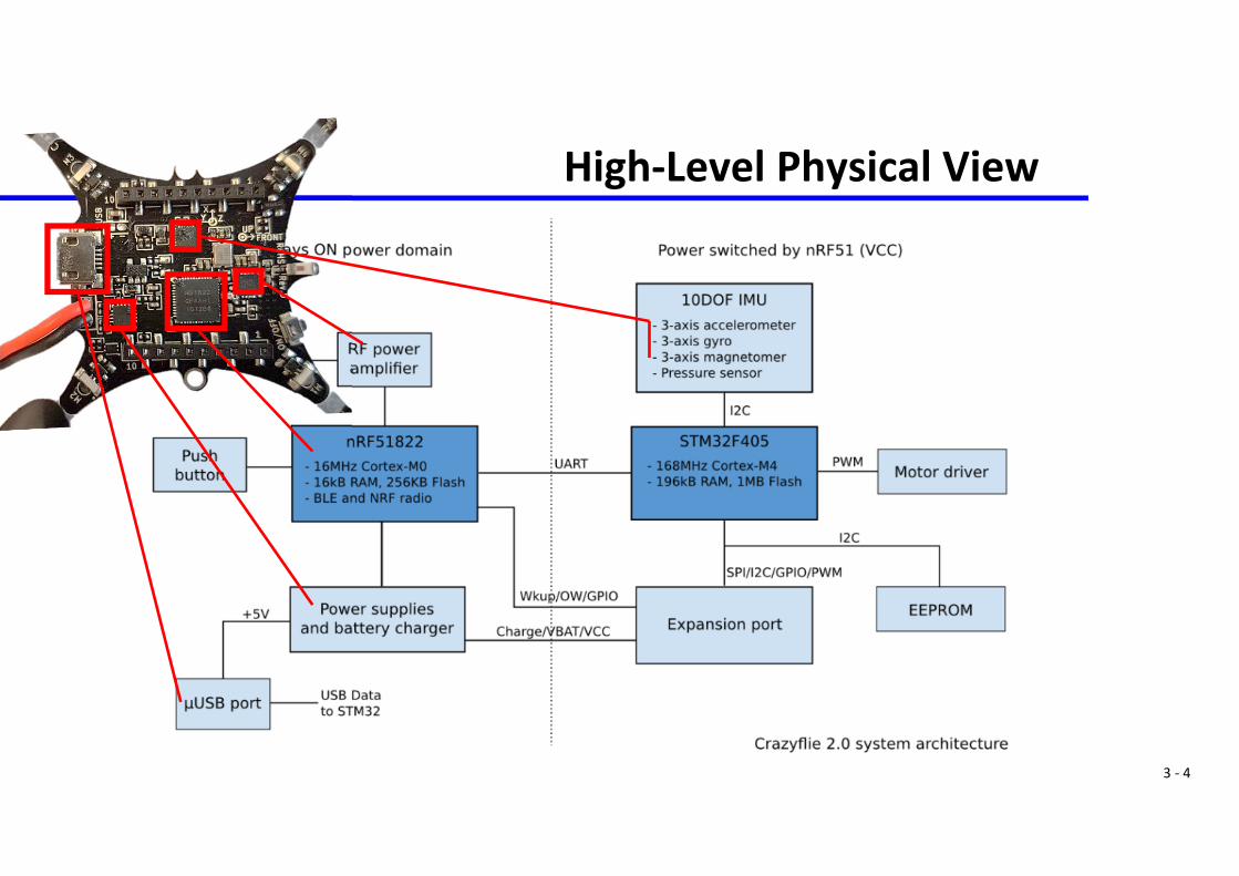
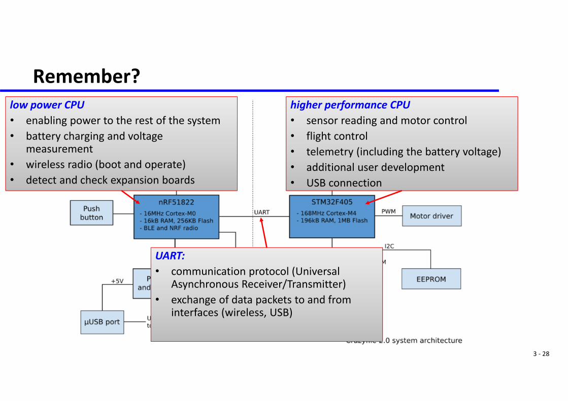
Remember?low power CPU• enabling power to the rest of the system• battery charging and voltage
measurement• wireless radio (boot and operate)• detect and check expansion boards
higher performance CPU• sensor reading and motor control• flight control• telemetry (including the battery voltage)• additional user development• USB connection
UART: • communication protocol (Universal
Asynchronous Receiver/Transmitter)• exchange of data packets to and from
interfaces (wireless, USB)

3 ‐ 29
Input and OutputUART Protocol
3 ‐ 30
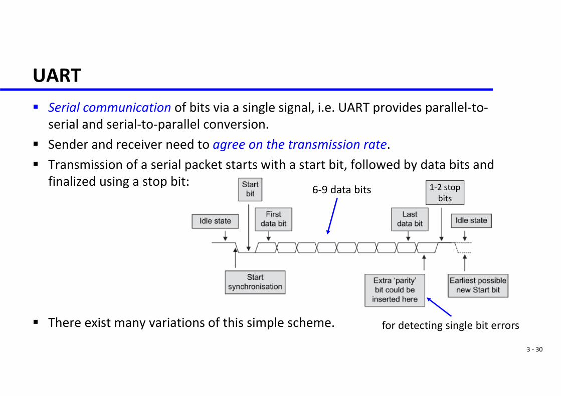
UART Serial communication of bits via a single signal, i.e. UART provides parallel‐to‐
serial and serial‐to‐parallel conversion. Sender and receiver need to agree on the transmission rate. Transmission of a serial packet starts with a start bit, followed by data bits and
finalized using a stop bit:
There exist many variations of this simple scheme. for detecting single bit errors
6‐9 data bits 1‐2 stopbits
3 ‐ 31
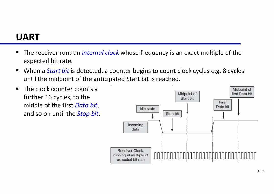
UART The receiver runs an internal clock whose frequency is an exact multiple of the
expected bit rate. When a Start bit is detected, a counter begins to count clock cycles e.g. 8 cycles
until the midpoint of the anticipated Start bit is reached. The clock counter counts a
further 16 cycles, to the middle of the first Data bit, and so on until the Stop bit.
3 ‐ 32
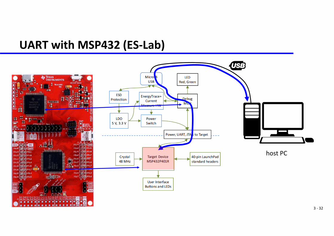
UART with MSP432 (ES‐Lab)
host PC
3 ‐ 33
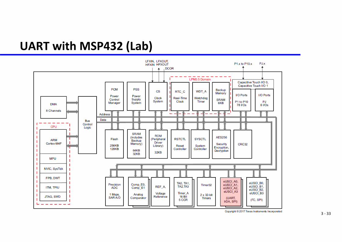
UART with MSP432 (Lab)
3 ‐ 34
Input and OutputMemory Mapped Device Access
3 ‐ 35
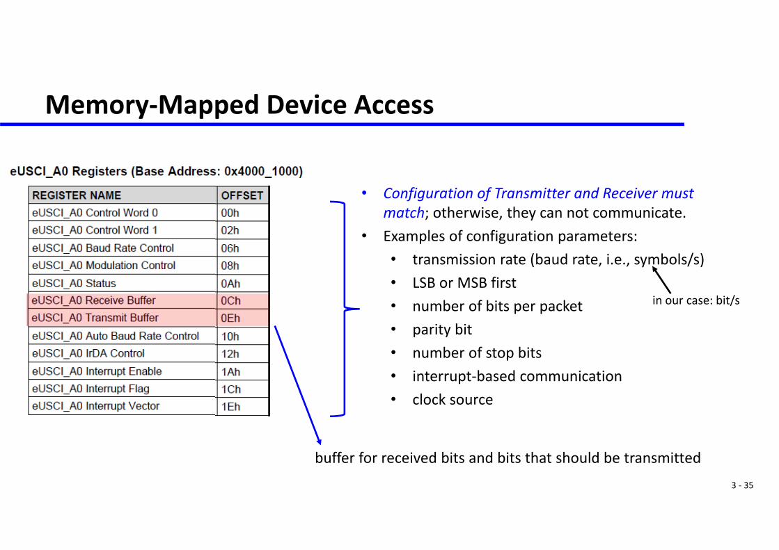
Memory‐Mapped Device Access
• Configuration of Transmitter and Receiver must match; otherwise, they can not communicate.
• Examples of configuration parameters:• transmission rate (baud rate, i.e., symbols/s)• LSB or MSB first• number of bits per packet• parity bit• number of stop bits• interrupt‐based communication• clock source
buffer for received bits and bits that should be transmitted
in our case: bit/s
3 ‐ 36
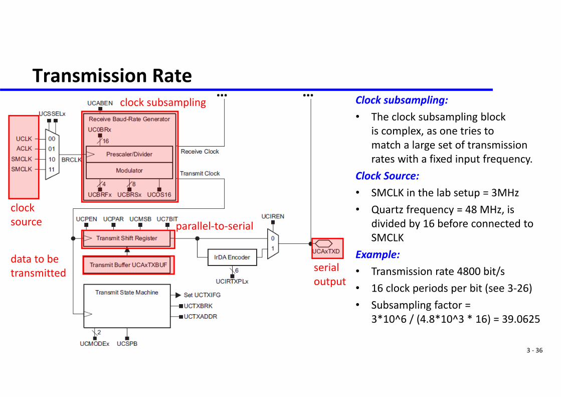
Transmission Rate
clocksource
clock subsampling……
serialoutput
parallel‐to‐serial
data to betransmitted
Clock subsampling:• The clock subsampling block
is complex, as one tries tomatch a large set of transmissionrates with a fixed input frequency.
Clock Source:• SMCLK in the lab setup = 3MHz• Quartz frequency = 48 MHz, is
divided by 16 before connected toSMCLK
Example: • Transmission rate 4800 bit/s• 16 clock periods per bit (see 3‐26)• Subsampling factor =
3*10^6 / (4.8*10^3 * 16) = 39.0625
3 ‐ 37
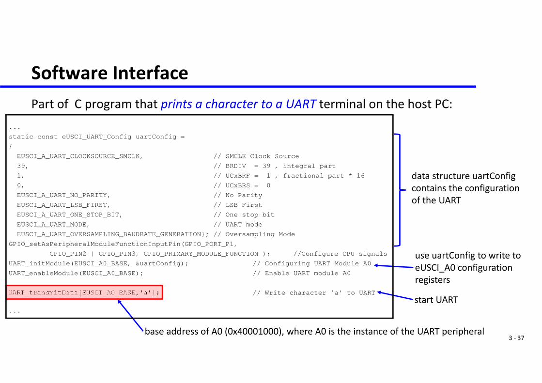
Software InterfacePart of C program that prints a character to a UART terminal on the host PC:
... static const eUSCI_UART_Config uartConfig =
{EUSCI_A_UART_CLOCKSOURCE_SMCLK, // SMCLK Clock Source
39, // BRDIV = 39 , integral part1, // UCxBRF = 1 , fractional part * 160, // UCxBRS = 0
EUSCI_A_UART_NO_PARITY, // No ParityEUSCI_A_UART_LSB_FIRST, // LSB First
EUSCI_A_UART_ONE_STOP_BIT, // One stop bitEUSCI_A_UART_MODE, // UART mode
EUSCI_A_UART_OVERSAMPLING_BAUDRATE_GENERATION}; // Oversampling ModeGPIO_setAsPeripheralModuleFunctionInputPin(GPIO_PORT_P1,
GPIO_PIN2 | GPIO_PIN3, GPIO_PRIMARY_MODULE_FUNCTION ); //Configure CPU signalsUART_initModule(EUSCI_A0_BASE, &uartConfig); // Configuring UART Module A0
UART_enableModule(EUSCI_A0_BASE); // Enable UART module A0
UART_transmitData(EUSCI_A0_BASE,'a'); // Write character ‘a’ to UART
...
data structure uartConfigcontains the configurationof the UART
use uartConfig to write toeUSCI_A0 configuration registers
start UART
base address of A0 (0x40001000), where A0 is the instance of the UART peripheral
3 ‐ 38
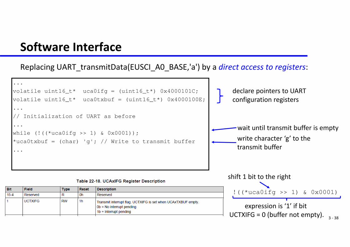
Software InterfaceReplacing UART_transmitData(EUSCI_A0_BASE,'a') by a direct access to registers:
... volatile uint16_t* uca0ifg = (uint16_t*) 0x4000101C;volatile uint16_t* uca0txbuf = (uint16_t*) 0x4000100E;... // Initialization of UART as before... while (!((*uca0ifg >> 1) & 0x0001));*uca0txbuf = (char) 'g'; // Write to transmit buffer...
declare pointers to UART configuration registers
wait until transmit buffer is emptywrite character ‘g’ to thetransmit buffer
!((*uca0ifg >> 1) & 0x0001)
shift 1 bit to the right
expression is ‘1’ if bit UCTXIFG = 0 (buffer not empty).

3 ‐ 39
Input and OutputSPI Protocol
3 ‐ 40
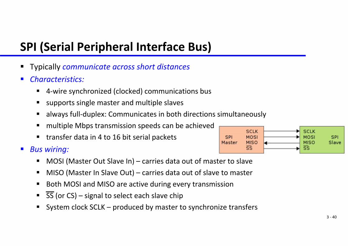
SPI (Serial Peripheral Interface Bus) Typically communicate across short distances Characteristics:
4‐wire synchronized (clocked) communications bus supports single master and multiple slaves always full‐duplex: Communicates in both directions simultaneously multiple Mbps transmission speeds can be achieved transfer data in 4 to 16 bit serial packets
Bus wiring: MOSI (Master Out Slave In) – carries data out of master to slave MISO (Master In Slave Out) – carries data out of slave to master Both MOSI and MISO are active during every transmission SS (or CS) – signal to select each slave chip System clock SCLK – produced by master to synchronize transfers

3 ‐ 41
SPI (Serial Peripheral Interface Bus)More detailed circuit diagram:
details vary betweendifferent vendors andimplementations
Timing diagram:
system clock SCLK
writing data output:
reading data inputin the middle of bit:
MOSI or MISO
3 ‐ 42
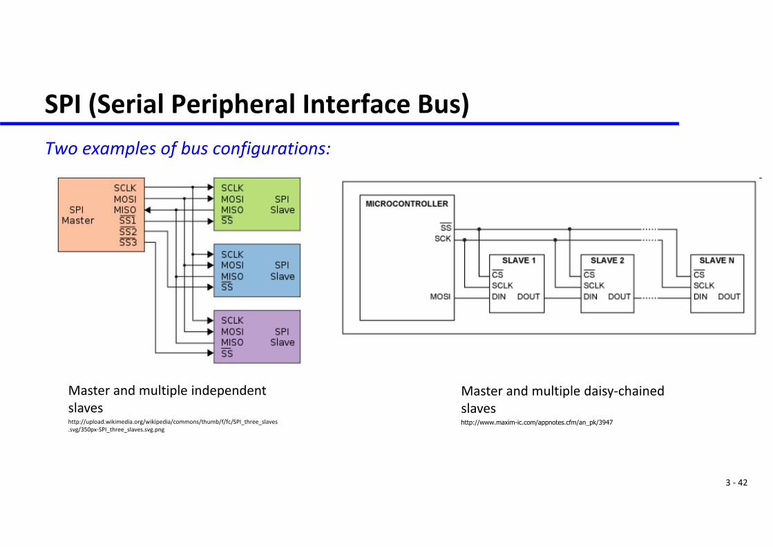
SPI (Serial Peripheral Interface Bus)Two examples of bus configurations:
Master and multiple independent slaveshttp://upload.wikimedia.org/wikipedia/commons/thumb/f/fc/SPI_three_slaves.svg/350px‐SPI_three_slaves.svg.png
Master and multiple daisy‐chained slaveshttp://www.maxim-ic.com/appnotes.cfm/an_pk/3947

3 ‐ 43
Interrupts

3 ‐ 44
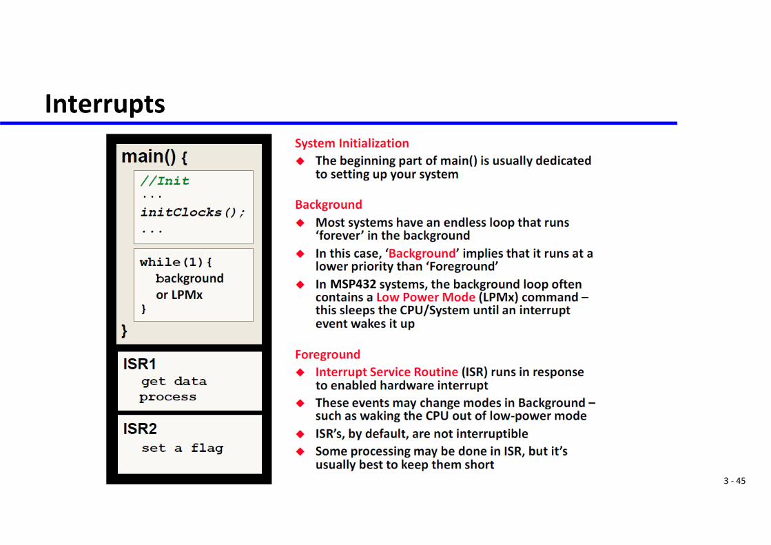
InterruptsA hardware interrupt is an electronic alerting signal sent to the CPU from another component, either from an internal peripheral or from an external device.
The Nested VectorInterrupt Controller(NVIC) handles theprocessing ofinterrupts
MSP 432 [ES‐Lab]
3 ‐ 45
Interrupts
. . .
MSP432

3 ‐ 46
Processing of an Interrupt (MSP432 ES‐Lab)
The vector interrupt controller (NVIC) enables and disables interrupts allows to individually and globally
mask interrupts (disable reaction to interrupt), and
registers interrupt service routines (ISR), sets the priority of interrupts.
Timer_A0
I/O Port P1
eUSCI_A0
peripheral unit
…
Nested VectorInterrupt Controller
(NVIC)CPU
interrupt handling
Interrupt priorities are relevant if several interrupts happen at the same time the programmer does not mask interrupts
in an interrupt service routine (ISR) and therefore, preemption of an ISR by another ISR may happen (interrupt nesting).
3 ‐ 47
Processing of an Interrupt
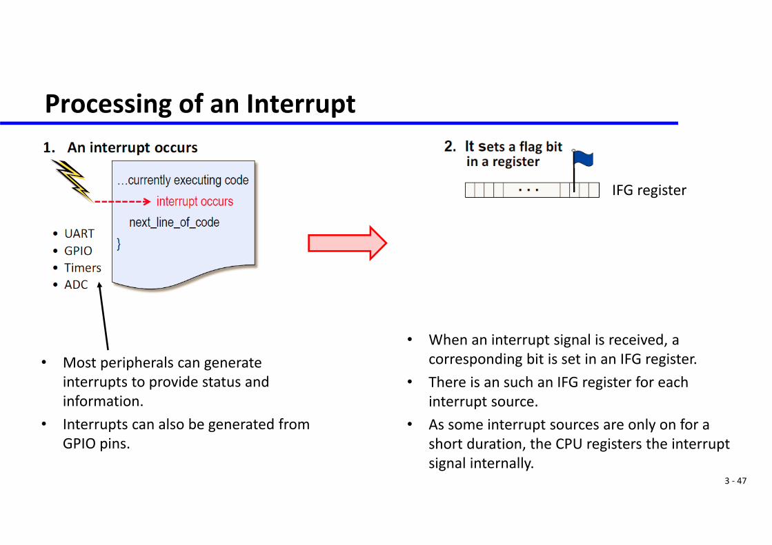
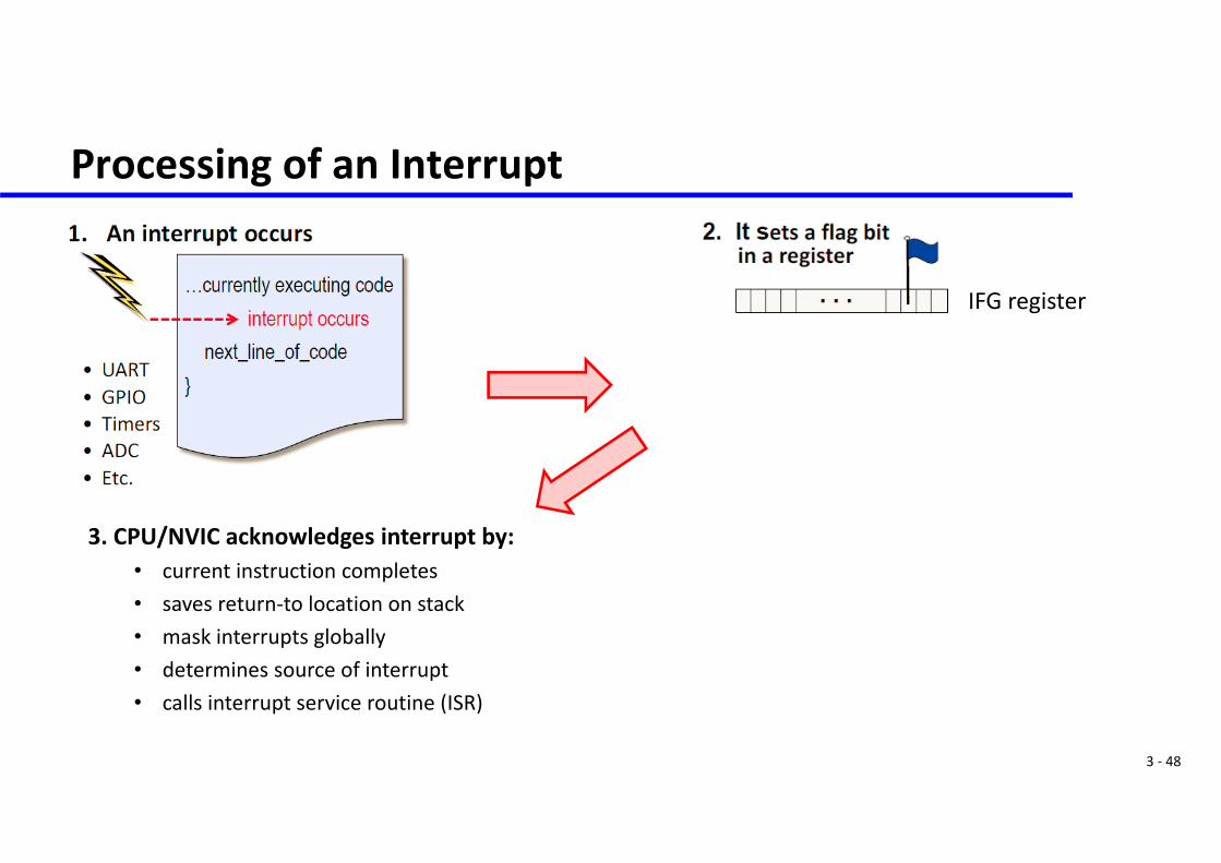
• Most peripherals can generate interrupts to provide status and information.
• Interrupts can also be generated from GPIO pins.
• When an interrupt signal is received, a corresponding bit is set in an IFG register.
• There is an such an IFG register for each interrupt source.
• As some interrupt sources are only on for a short duration, the CPU registers the interrupt signal internally.
IFG register
3 ‐ 48
Processing of an Interrupt
IFG register
3. CPU/NVIC acknowledges interrupt by:• current instruction completes• saves return‐to location on stack• mask interrupts globally• determines source of interrupt• calls interrupt service routine (ISR)
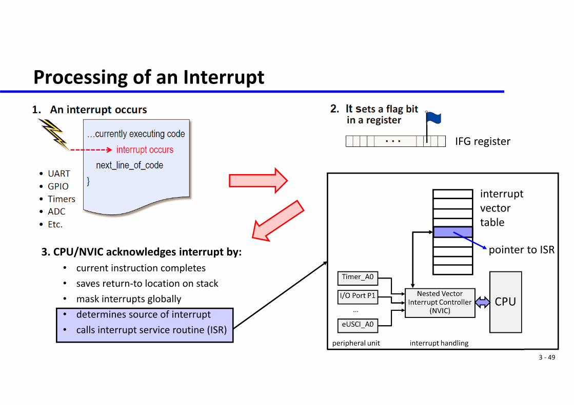
3 ‐ 49
Processing of an Interrupt
IFG register
3. CPU/NVIC acknowledges interrupt by:• current instruction completes• saves return‐to location on stack• mask interrupts globally• determines source of interrupt• calls interrupt service routine (ISR)
interruptvectortable
pointer to ISR
3 ‐ 50
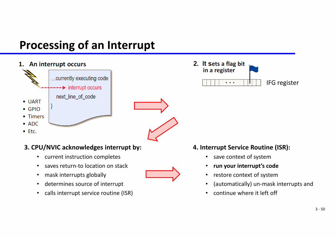
Processing of an Interrupt
IFG register
3. CPU/NVIC acknowledges interrupt by:• current instruction completes• saves return‐to location on stack• mask interrupts globally• determines source of interrupt• calls interrupt service routine (ISR)
4. Interrupt Service Routine (ISR):• save context of system• run your interrupt’s code• restore context of system• (automatically) un‐mask interrupts and• continue where it left off
3 ‐ 51
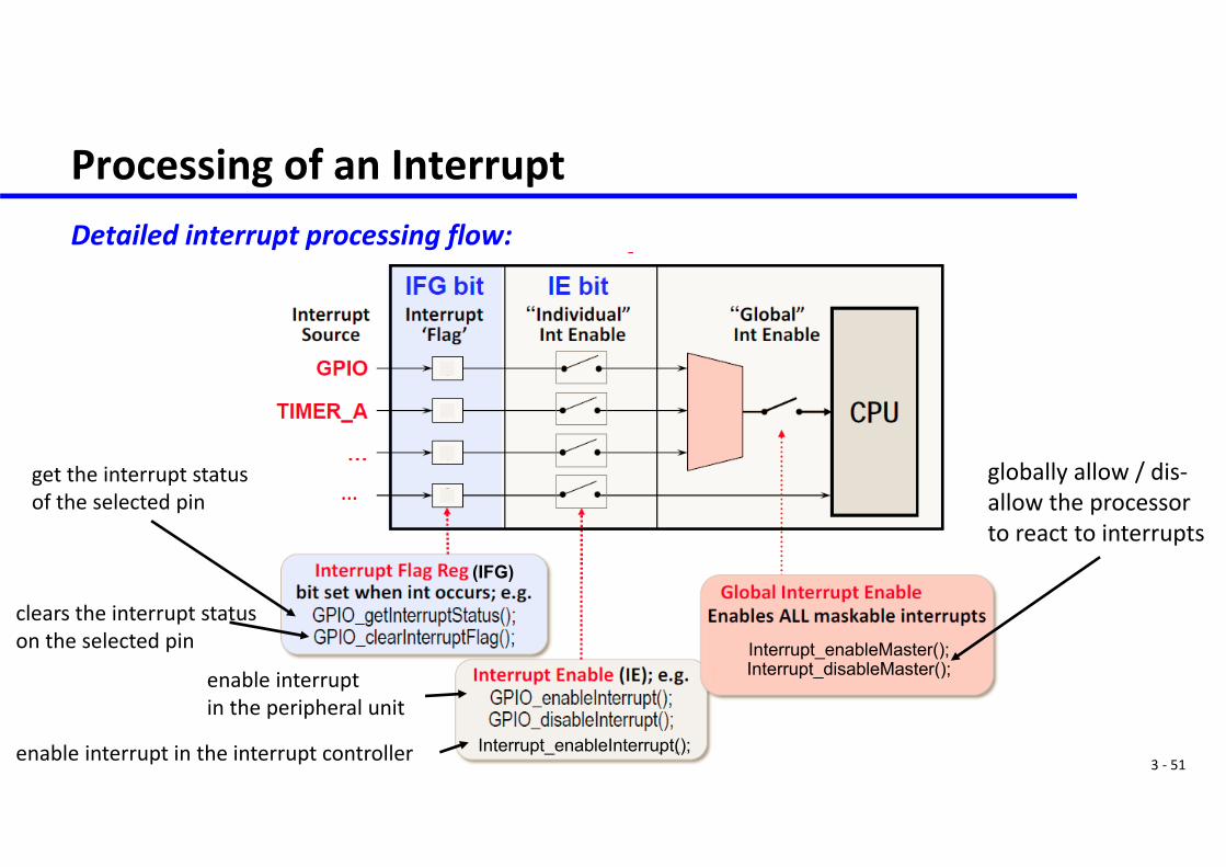
Processing of an InterruptDetailed interrupt processing flow:
(IFG)
Interrupt_enableInterrupt();
Interrupt_enableMaster();Interrupt_disableMaster();
globally allow / dis‐allow the processorto react to interrupts
enable interruptin the peripheral unit
enable interrupt in the interrupt controller
get the interrupt status of the selected pin
clears the interrupt status on the selected pin
…
3 ‐ 52
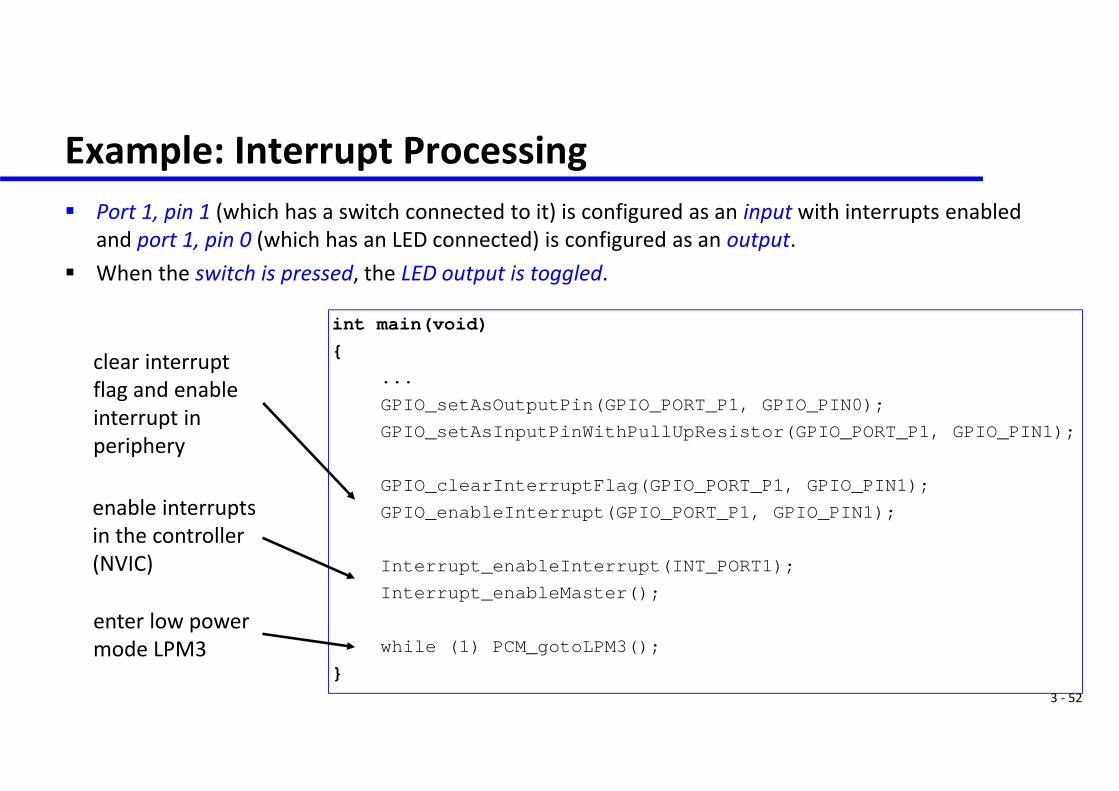
Example: Interrupt Processing Port 1, pin 1 (which has a switch connected to it) is configured as an input with interrupts enabled
and port 1, pin 0 (which has an LED connected) is configured as an output. When the switch is pressed, the LED output is toggled.
int main(void){
•...•GPIO_setAsOutputPin(GPIO_PORT_P1, GPIO_PIN0);•GPIO_setAsInputPinWithPullUpResistor(GPIO_PORT_P1, GPIO_PIN1);
•GPIO_clearInterruptFlag(GPIO_PORT_P1, GPIO_PIN1);•GPIO_enableInterrupt(GPIO_PORT_P1, GPIO_PIN1);
•Interrupt_enableInterrupt(INT_PORT1);•Interrupt_enableMaster();
•while (1) PCM_gotoLPM3();}
enter low powermode LPM3
enable interruptsin the controller(NVIC)
clear interruptflag and enableinterrupt in periphery
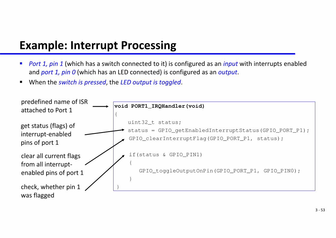
3 ‐ 53
Example: Interrupt Processing Port 1, pin 1 (which has a switch connected to it) is configured as an input with interrupts enabled
and port 1, pin 0 (which has an LED connected) is configured as an output. When the switch is pressed, the LED output is toggled.
check, whether pin 1was flagged
get status (flags) ofinterrupt‐enabledpins of port 1
predefined name of ISRattached to Port 1
void PORT1_IRQHandler(void){
uint32_t status;status = GPIO_getEnabledInterruptStatus(GPIO_PORT_P1);•GPIO_clearInterruptFlag(GPIO_PORT_P1, status);
•if(status & GPIO_PIN1)•{• GPIO_toggleOutputOnPin(GPIO_PORT_P1, GPIO_PIN0);•}
•}
clear all current flagsfrom all interrupt‐enabled pins of port 1
3 ‐ 54
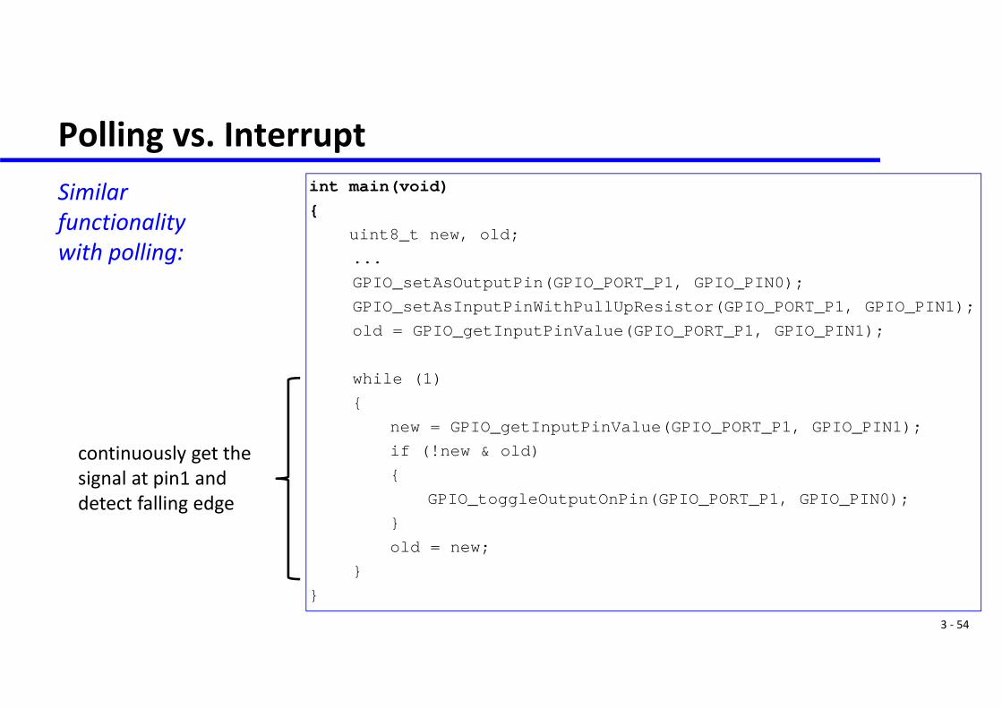
Polling vs. InterruptSimilar functionality with polling:
int main(void) {
uint8_t new, old;•...•GPIO_setAsOutputPin(GPIO_PORT_P1, GPIO_PIN0);•GPIO_setAsInputPinWithPullUpResistor(GPIO_PORT_P1, GPIO_PIN1);•old = GPIO_getInputPinValue(GPIO_PORT_P1, GPIO_PIN1);
•while (1) •{
•new = GPIO_getInputPinValue(GPIO_PORT_P1, GPIO_PIN1);•if (!new & old) •{
•GPIO_toggleOutputOnPin(GPIO_PORT_P1, GPIO_PIN0);•}•old = new;
•}}
continuously get thesignal at pin1 anddetect falling edge
3 ‐ 55
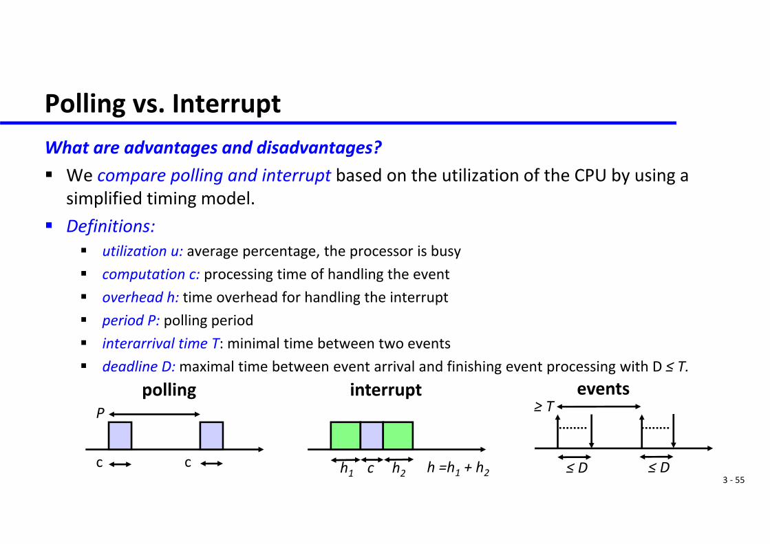
Polling vs. InterruptWhat are advantages and disadvantages? We compare polling and interrupt based on the utilization of the CPU by using a
simplified timing model. Definitions:
utilization u: average percentage, the processor is busy computation c: processing time of handling the event overhead h: time overhead for handling the interrupt period P: polling period interarrival time T: minimal time between two events deadline D: maximal time between event arrival and finishing event processing with D ≤ T.
polling
c c
Pinterrupt
c h2h1 h =h1 + h2
events≥ T
≤ D ≤ D
3 ‐ 56
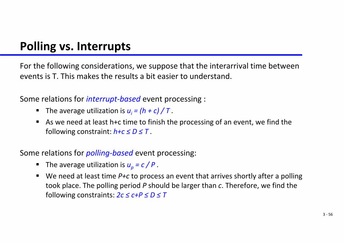
Polling vs. InterruptsFor the following considerations, we suppose that the interarrival time between events is T. This makes the results a bit easier to understand.
Some relations for interrupt‐based event processing : The average utilization is ui = (h + c) / T . As we need at least h+c time to finish the processing of an event, we find the
following constraint: h+c ≤ D ≤ T .
Some relations for polling‐based event processing: The average utilization is up = c / P . We need at least time P+c to process an event that arrives shortly after a polling
took place. The polling period P should be larger than c. Therefore, we find the following constraints: 2c ≤ c+P ≤ D ≤ T
3 ‐ 57
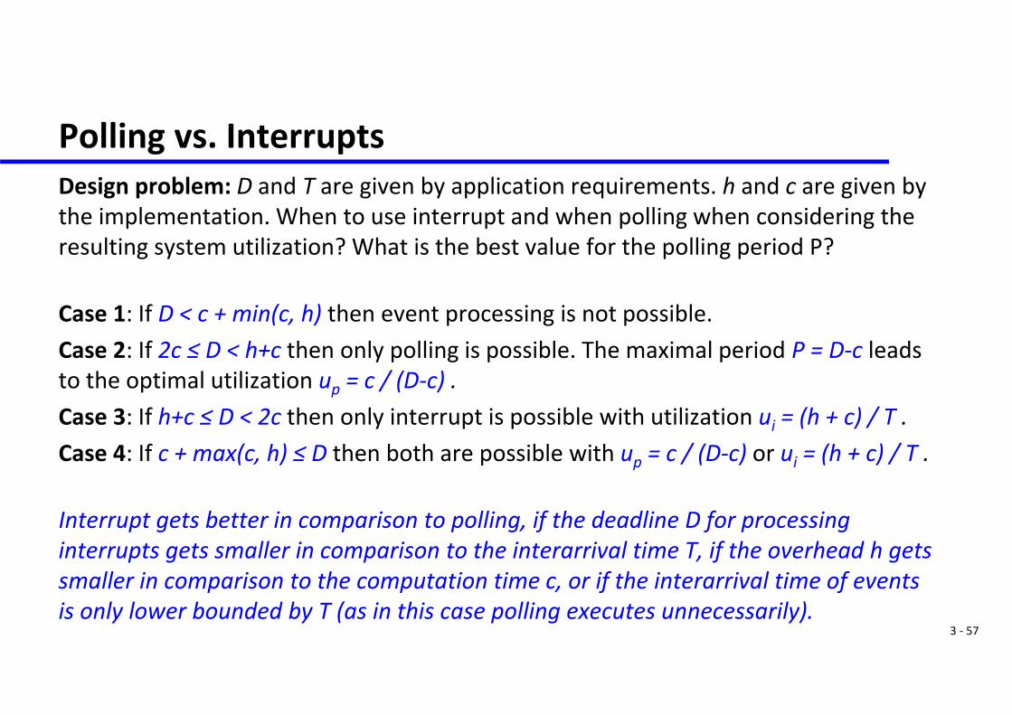
Polling vs. InterruptsDesign problem: D and T are given by application requirements. h and c are given by the implementation. When to use interrupt and when polling when considering the resulting system utilization? What is the best value for the polling period P?
Case 1: If D < c + min(c, h) then event processing is not possible.Case 2: If 2c ≤ D < h+c then only polling is possible. The maximal period P = D‐c leads to the optimal utilization up = c / (D‐c) . Case 3: If h+c ≤ D < 2c then only interrupt is possible with utilization ui = (h + c) / T .Case 4: If c + max(c, h) ≤ D then both are possible with up = c / (D‐c) or ui = (h + c) / T .
Interrupt gets better in comparison to polling, if the deadline D for processing interrupts gets smaller in comparison to the interarrival time T, if the overhead h gets smaller in comparison to the computation time c, or if the interarrival time of events is only lower bounded by T (as in this case polling executes unnecessarily).

3 ‐ 58
Clocks and Timers

3 ‐ 59
Clocks and TimersClocks
3 ‐ 60
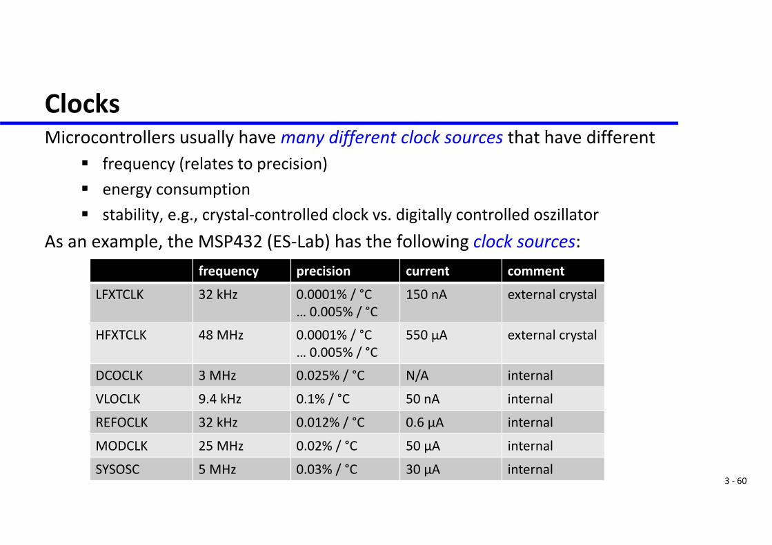
ClocksMicrocontrollers usually have many different clock sources that have different
frequency (relates to precision) energy consumption stability, e.g., crystal‐controlled clock vs. digitally controlled oszillator
As an example, the MSP432 (ES‐Lab) has the following clock sources:frequency precision current comment
LFXTCLK 32 kHz 0.0001% / °C… 0.005% / °C
150 nA external crystal
HFXTCLK 48 MHz 0.0001% / °C… 0.005% / °C
550 µA external crystal
DCOCLK 3 MHz 0.025% / °C N/A internal
VLOCLK 9.4 kHz 0.1% / °C 50 nA internal
REFOCLK 32 kHz 0.012% / °C 0.6 µA internal
MODCLK 25 MHz 0.02% / °C 50 µA internal
SYSOSC 5 MHz 0.03% / °C 30 µA internal
3 ‐ 61
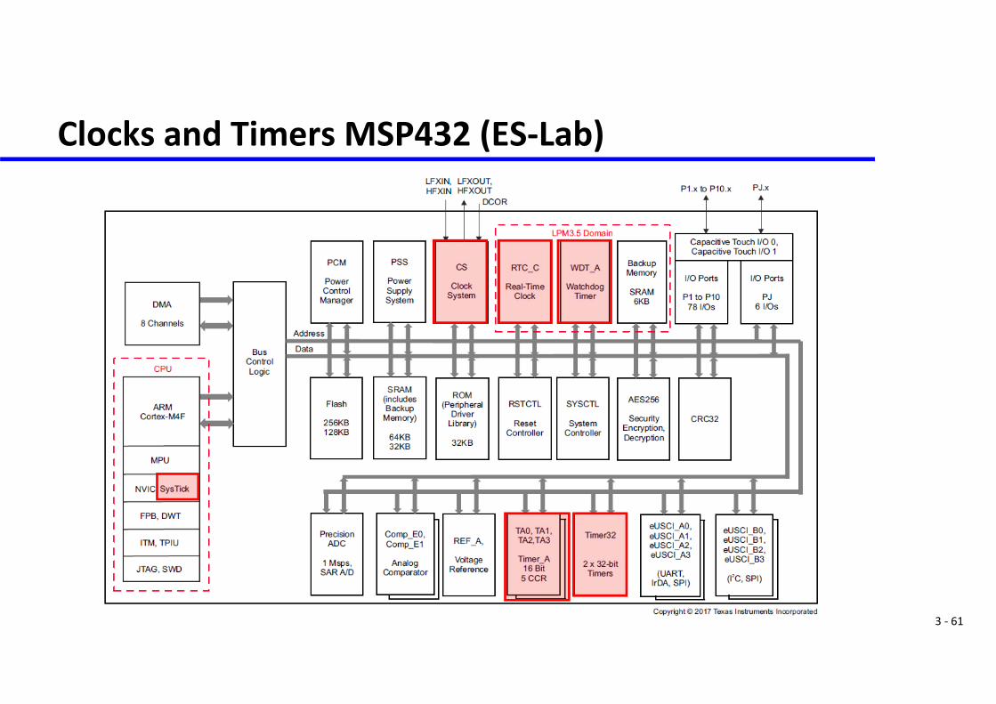
Clocks and Timers MSP432 (ES‐Lab)
3 ‐ 62
Clocks and Timers MSP432 (ES‐Lab)
3 ‐ 63
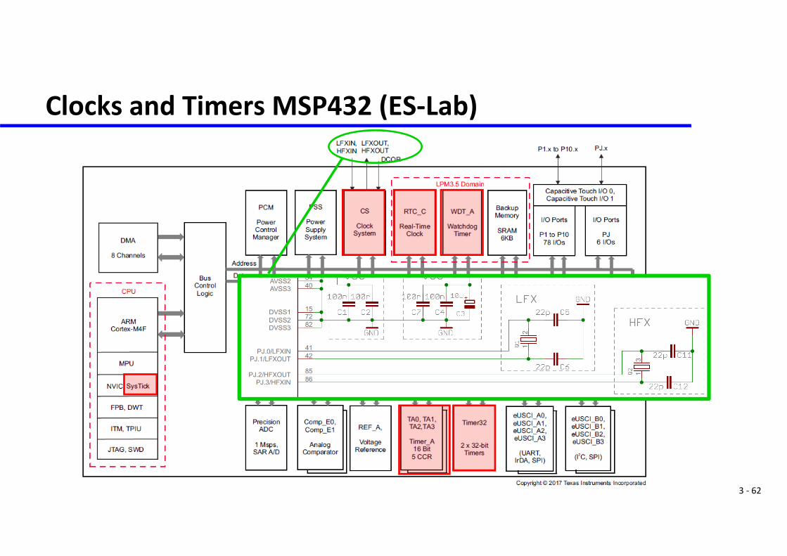
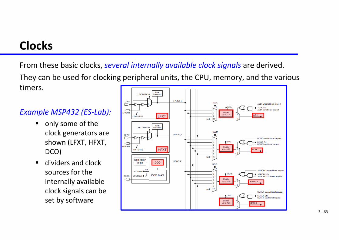
ClocksFrom these basic clocks, several internally available clock signals are derived. They can be used for clocking peripheral units, the CPU, memory, and the various timers.
Example MSP432 (ES‐Lab): only some of the
clock generators areshown (LFXT, HFXT,DCO)
dividers and clocksources for the internally availableclock signals can beset by software

3 ‐ 64
Clocks and TimersWatchdog Timer

3 ‐ 65
Watchdog TimerWatchdog Timers provide system fail‐safety:
If their counter ever rolls over (back to zero), they reset the processor. The goal here is to prevent your system from being inactive (deadlock) due to some unexpected fault.
To prevent your system from continuously resetting itself, the counter should be reset at appropriate intervals. CPU Watchdog Timer (WDT_A)
reset
reset counter to 0
clock input, e.g.,SMCLK, ACLK
If the count completes without a restart,the CPU is reset.
WDT_A_clearTimer();
up counter
•WDT_A_holdTimer(); pause counting up
overflow
3 ‐ 66
Clocks and TimersSystem Tick

3 ‐ 67
SysTick MSP432 (ES‐Lab) SysTick is a simple decrementing 24 bit counter that is part of the NVIC
controller (Nested Vector Interrupt Controller). Its clock source is MCLK and it reloads to period‐1 after reaching 0.
It’s a very simple timer, mainly used for periodic interrupts or measuring time.int main(void) {
...GPIO_setAsOutputPin(GPIO_PORT_P1, GPIO_PIN0);
SysTick_enableModule();SysTick_setPeriod(1500000);SysTick_enableInterrupt();Interrupt_enableMaster();
while (1) PCM_gotoLPM0();
void SysTick_Handler(void) {MAP_GPIO_toggleOutputOnPin(GPIO_PORT_P1, GPIO_PIN0); }
if MCLK has a frequency of 3 MHz,an interrupt is generated every 0.5 s.
go to low power mode LP0 after executing the ISR
3 ‐ 68
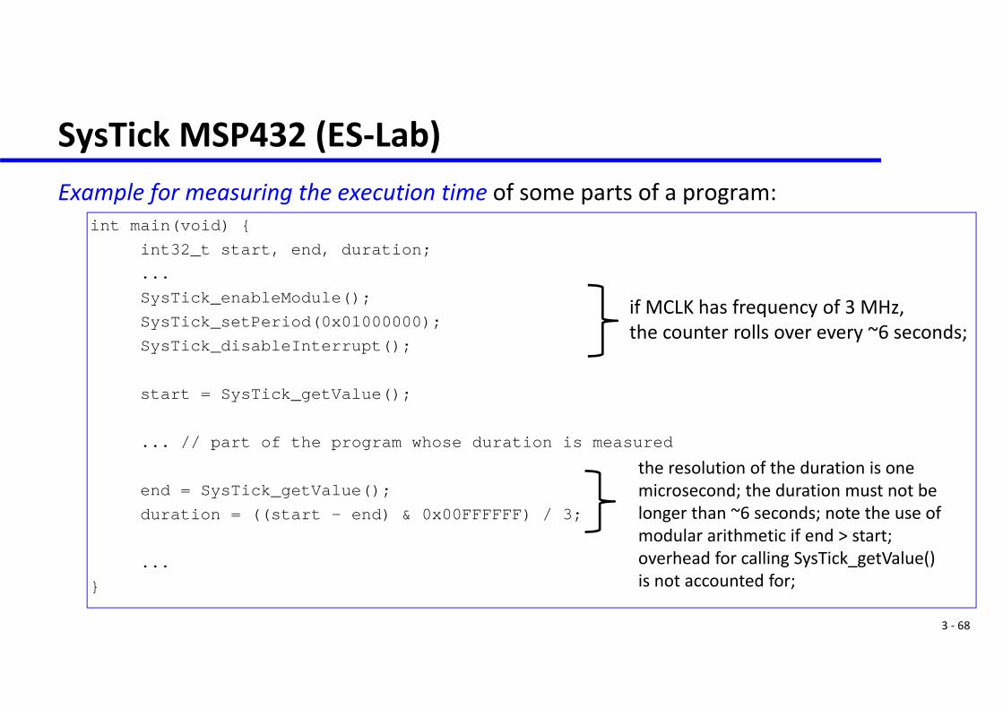
SysTick MSP432 (ES‐Lab)Example for measuring the execution time of some parts of a program:
int main(void) { int32_t start, end, duration;...SysTick_enableModule();SysTick_setPeriod(0x01000000);SysTick_disableInterrupt();
start = SysTick_getValue();
... // part of the program whose duration is measured
end = SysTick_getValue();duration = ((start - end) & 0x00FFFFFF) / 3;
... }
if MCLK has frequency of 3 MHz,the counter rolls over every ~6 seconds;
the resolution of the duration is one microsecond; the duration must not be longer than ~6 seconds; note the use of modular arithmetic if end > start;overhead for calling SysTick_getValue()is not accounted for;

3 ‐ 69
Clocks and TimersTimer and PWM
3 ‐ 70
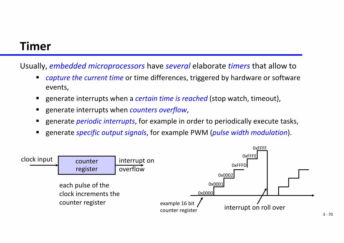
TimerUsually, embedded microprocessors have several elaborate timers that allow to
capture the current time or time differences, triggered by hardware or software events,
generate interrupts when a certain time is reached (stop watch, timeout), generate interrupts when counters overflow, generate periodic interrupts, for example in order to periodically execute tasks, generate specific output signals, for example PWM (pulse width modulation).
counterregister
clock input interrupt onoverflow
each pulse of the clock increments the counter register
0x0000
0x0001
0x0002
0xFFFD
0xFFFE
0xFFFF
interrupt on roll overexample 16 bitcounter register
3 ‐ 71
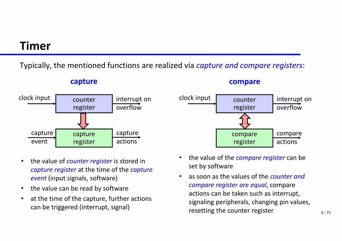
TimerTypically, the mentioned functions are realized via capture and compare registers:
counterregister
clock input interrupt onoverflow
counterregister
clock input interrupt onoverflow
captureregister
compareregister
capture event
captureactions
• the value of counter register is stored in capture register at the time of the capture event (input signals, software)
• the value can be read by software• at the time of the capture, further actions
can be triggered (interrupt, signal)
compareactions
• the value of the compare register can be set by software
• as soon as the values of the counter and compare register are equal, compare actions can be taken such as interrupt, signaling peripherals, changing pin values,resetting the counter register
capture compare

3 ‐ 72
Timer Pulse Width Modulation (PWM) can be used to change the average power of a
signal. The use case could be to change the speed of a motor or to modulate the light
intensity of an LED.counterregister
0x0000
0xFFFF one compare registeris used to define the period
another compare register is used to change the duty cycle of the signal
output signal
3 ‐ 73
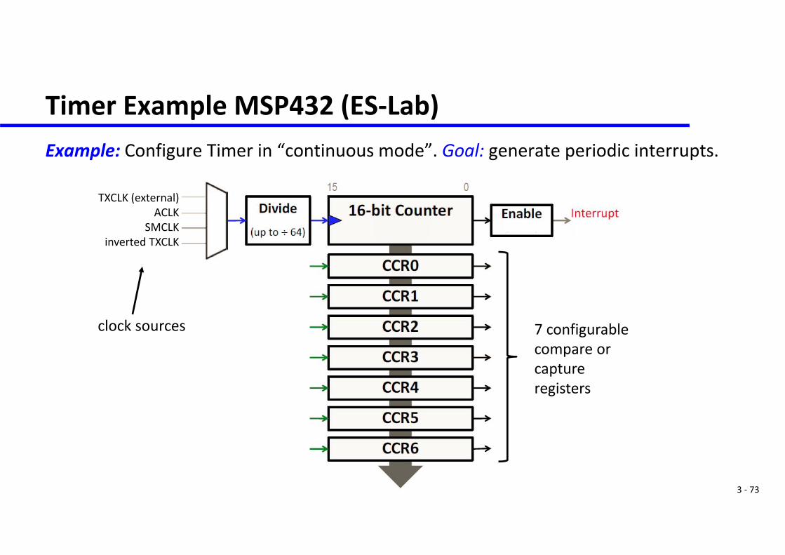
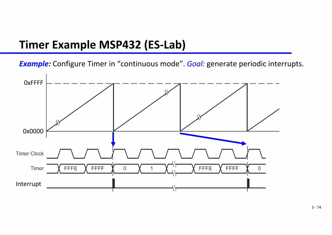
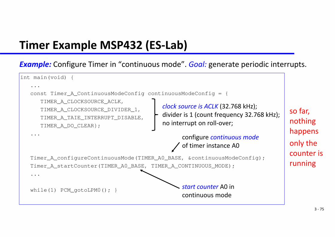
Timer Example MSP432 (ES‐Lab)Example: Configure Timer in “continuous mode”. Goal: generate periodic interrupts.
TXCLK (external)ACLK
SMCLKinverted TXCLK
clock sources 7 configurablecompare orcaptureregisters
3 ‐ 74
Timer Example MSP432 (ES‐Lab)Example: Configure Timer in “continuous mode”. Goal: generate periodic interrupts.
0x0000
0xFFFF
Interrupt
3 ‐ 75
Timer Example MSP432 (ES‐Lab)Example: Configure Timer in “continuous mode”. Goal: generate periodic interrupts.int main(void) {
...const Timer_A_ContinuousModeConfig continuousModeConfig = {
TIMER_A_CLOCKSOURCE_ACLK, TIMER_A_CLOCKSOURCE_DIVIDER_1,TIMER_A_TAIE_INTERRUPT_DISABLE,TIMER_A_DO_CLEAR};
...
Timer_A_configureContinuousMode(TIMER_A0_BASE, &continuousModeConfig);Timer_A_startCounter(TIMER_A0_BASE, TIMER_A_CONTINUOUS_MODE);...
while(1) PCM_gotoLPM0(); }
clock source is ACLK (32.768 kHz);divider is 1 (count frequency 32.768 kHz);no interrupt on roll‐over;
configure continuous mode of timer instance A0
start counter A0 in continuous mode
so far, nothing happensonly thecounter is running
3 ‐ 76
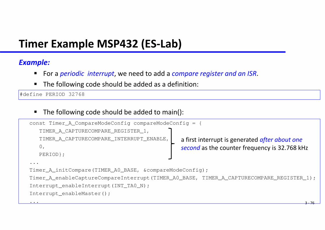
Timer Example MSP432 (ES‐Lab)Example:
For a periodic interrupt, we need to add a compare register and an ISR. The following code should be added as a definition:
The following code should be added to main():const Timer_A_CompareModeConfig compareModeConfig = {
TIMER_A_CAPTURECOMPARE_REGISTER_1,TIMER_A_CAPTURECOMPARE_INTERRUPT_ENABLE,0,PERIOD};
...Timer_A_initCompare(TIMER_A0_BASE, &compareModeConfig);Timer_A_enableCaptureCompareInterrupt(TIMER_A0_BASE, TIMER_A_CAPTURECOMPARE_REGISTER_1);Interrupt_enableInterrupt(INT_TA0_N);Interrupt_enableMaster();...
a first interrupt is generated after about one second as the counter frequency is 32.768 kHz
#define PERIOD 32768
3 ‐ 77
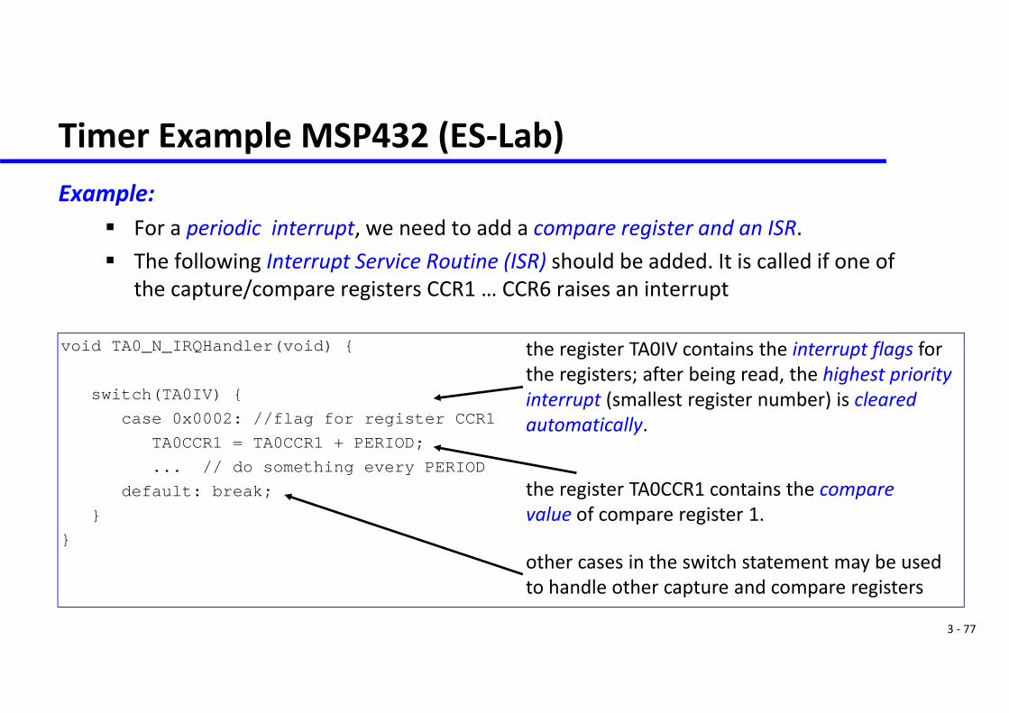
Timer Example MSP432 (ES‐Lab)Example:
For a periodic interrupt, we need to add a compare register and an ISR. The following Interrupt Service Routine (ISR) should be added. It is called if one of
the capture/compare registers CCR1 … CCR6 raises an interrupt
void TA0_N_IRQHandler(void) {
switch(TA0IV) {case 0x0002: //flag for register CCR1
TA0CCR1 = TA0CCR1 + PERIOD;... // do something every PERIOD
default: break; }
}
the register TA0IV contains the interrupt flags for the registers; after being read, the highest priority interrupt (smallest register number) is clearedautomatically.
other cases in the switch statement may be used to handle other capture and compare registers
the register TA0CCR1 contains the compare value of compare register 1.
3 ‐ 78
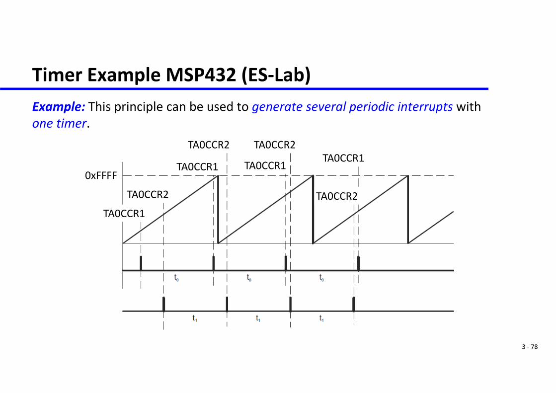
Timer Example MSP432 (ES‐Lab)Example: This principle can be used to generate several periodic interrupts with one timer.
0xFFFF
TA0CCR1
TA0CCR1 TA0CCR1TA0CCR1
TA0CCR2
TA0CCR2 TA0CCR2
TA0CCR2
Top Related