


Languages
Pages
Legal

ELECTROVALUE „„„„Electric and Electronic EcoElectric and Electronic EcoElectric and Electronic EcoElectric and Electronic Eco----assembly Alternatives for the assembly Alternatives for the assembly Alternatives for the assembly Alternatives for the
Valorisation of the EndValorisation of the EndValorisation of the EndValorisation of the End----ofofofof----life Products in the Recycling Marketlife Products in the Recycling Marketlife Products in the Recycling Marketlife Products in the Recycling Market‰‰‰‰
LIFE07 ENV/P/000639
Document Title: Training Courses
Version: 1 Deliverable no: D.8.1
Date: April 2011 Company: ISQ
Author(s):
ISQ
Level of Dissemination (PU/CO): PU
Distribution List: All partners and public in general
Abstract:
This document presents a literature review and analysis of the most suitable soldering techniques.
Documents included: -
Notes: 47 pages, including cover

i
Table of Contents List of Abbreviations........................................................................................................ ii
1. SOLDERING...............................................................................................................3
1.1. TECHNIQUES .....................................................................................................4
1.2. TIPS & TROUBLESHOOTING GUIDE......................................................................9
1.3. WORK PREPARATION.......................................................................................11
2. DESOLDERING COMPONENTS...................................................................................13
2.1. INTRODUCTION ................................................................................................13
2.2. TOOLS ............................................................................................................13
2.3. DESOLDERING PROCESS .................................................................................15
2.4. DESOLDERING T ECHNIQUES ............................................................................30
2.5. TIPS ...............................................................................................................32
3. COMPONENTS .........................................................................................................33
4. SAFETY ..................................................................................................................36
4.1. FIRST AID........................................................................................................36
4.2. SECURITY @ WORK.........................................................................................36
4.2.1. CONTAMINATION..........................................................................................37
4.2.2. HANDLING OF ELECTRONIC CIRCUITS............................................................37
4.2.3. GLOVES AND VINGERCOTS ...........................................................................37
5. GLOSSARY..............................................................................................................38
6. REFERENCES..............................................................................................................45

D.8.1 – Training Courses
ii
List of Abbreviations
DIP – Dual-inline Package
IC – Integrated Circuits
LED – Light emitting diode
PCB – Printed Circuit Board
PLCC – Plastic Leaded Chip Carrier
PTH – Plated Through-Hole
SMD – Surface-mount Device
SMT – Surface Mount

D.8.1 – Training Courses
3
1. SOLDERING
Soldering is accomplished by quickly heating the metal parts to be joined, and then
applying a flux and a solder to the mating surfaces. The finished solder joint
metallurgically bonds the parts - forming an excellent electrical connection between
wires and a strong mechanical joint between the metal parts. Heat is supplied with a
soldering iron or other means. The flux is a chemical cleaner which prepares the hot
surfaces for the molten solder. The solder is a low melting point alloy of non ferrous
metals.
The base material in a solder connection consists of the component and the plated
circuit traces on the printed circuit board (PCB). The mass, composition, and cleanliness
of the base material all determine the ability of the solder to flow and adhere properly
(wet) and provide a reliable connection.
If the base material has surface contamination, this action prevents the solder from
wetting along the surface of the board material. Component leads are usually protected
by a surface finish. The surface finishes can vary from plated tin to a solder - dipped
coating.
Figure 1: Proper welding technique (source: Circuit Technology Center)

D.8.1 – Training Courses
4
1.1. TECHNIQUES
A. Wetting Action
Wetting Action is the ability of a liquid to spread out and adhere to a solid
surface. It can be seen as a metal solvent action which takes place when
sufficient heat is applied to a connection allowing the solder to liquefy. When the
hot solder comes in contact with the surface, a metal solvent action takes place.
The solder dissolves and penetrates the surface. The molecules of solder and
copper blend to form a new alloy. This solvent action is called wetting and forms
the intermetallic bond between the parts. Wetting can only occur if the surface of
the copper is free of contamination and from the oxide film that forms when the
metal is exposed to air. Also, the solder and work surface need to have reached
the proper temperature. Although the surfaces to be soldered may look clean, there is
always a thin film of oxide covering it. For a good solder bond, surface oxides must be
removed during the soldering process using flux.
Figure 2: ’Wetting’ occurs when molten solder penetrates the surface, forming an
intermetallic bond.
B. Through Hole Mount
Through hole mounting refers to the mounting scheme used for electronic components
which involves the use of leads on the components that are inserted into holes drilled in
PCB and soldered to pads on the opposite side either by manual assembly, by hand
placement or by the use of automated insertion mount machines.

D.8.1 – Training Courses
5
Step 1: Use a small eraser to remove any oxidation from the solder pads.
Step 2: Apply a small amount Isopropyl alcohol to each pad that needs to be soldered.
Use the cotton swab to this.
Step 3: Select and install the appropriate soldering tip.
Step 4: Using the OKI soldering station turn the power on.
Step 5: Allow the soldering tip to warm up for 1 minute.
Step 6: Insert the through-hole component into the PCB.
Step 7: Flip the PCB over and ensure the component does not shift or slip. If the
component does shift, you can try bending the leads to keep the component installed.
Step 8: Put a small dot of flux on each pad to soldered (not always necessary).
Step 9: Tin the soldering tip by melting a small amount of solder to it.
Step 10: Clean the tip with wire pad.
Step 11: Touch the soldering tip to pad and heat the pad. After 3 seconds or so, feed
the solder into the joint as shown in figure 41.
Step 12: After all the soldering on the PCB is completed, clean the board with isopropyl
alcohol to remove any flux residue.
Step 13: With compressed air blow the board dry.
Step 14: Avoid rapid heating of ceramic chip capacitors during soldering operations.
C. Surface Mount (SMT)
Surface mounting refers to the method by which components are mounted directly on
the surface of PCB, allowing the use of both sides. Electronic components created in this
way are called surface-mount devices (SMD). In industry, has replaced the large-scale
assembly method PTH. An SMT component is usually smaller than its equivalent PTH,
because it has a shorter terminal or sometimes not even has them. The terminals also
vary in shape, may have flat contacts, arrays of solder balls (BGAs) or terminators in the
body of the component. In SMT, machines are typically used inserter components
throughout the production process, from application of solder paste even the assembly

D.8.1 – Training Courses
6
of components and the melting of solder paste, because the components are usually
very small, sensitive and need high-precision assembly, requiring a very strict control of
process parameters.
Figure 3: Example of SMT assembly
Figure 4: Examples of devices for SMT.

D.8.1 – Training Courses
7
Step 1: Appling solder paste by syringe to each
pad that requires soldering.
Step 2: Position the component on the pads.
Step 3: Place the PCB with the solder paste and
components in a soldering oven.
Step 4: After allowing the PCB’s to cool wash the
PCB.
Step 5: Inspect the boards for misaligned
components, solder bridge, or missing solder.
Step 6: Perform any necessary rework.

D.8.1 – Training Courses
8
Figure 5: Adding Solder to One SMT Pad
Figure 6: Fixing One Side of a Component
Figure 7: Fixing the Second Side of a
Component
Figure 8: The Soldered SMT Component.
The amount of solder paste used is important the following figure give a visual indication
of what too much and too little paste can look like:
Figure 9: SMT Examples with too much
solder used.
Figure 10: SMT Examples with the correct amount of solder used
Figure 11: SMT Examples with too little solder used

D.8.1 – Training Courses
9
1.2. TIPS & TROUBLESHOOTING GUIDE
General Soldering Advice
o Clean all parts to be soldered.
o The most important aspect to soldering is having a good tinned soldering tip. The
heat will tend to oxidize the tip. An oxidized tip will repel solder. To tin the tip,
wipe it on a wet sponge, and melt a glob of solder onto it, and then wipe it again.
o Keep the soldering tip at a lower temperature, around 700F so that pads don't get
lifted and so parts are not damaged.
o Regularly replace your tips. If you are constantly using it, then once a month is
not unreasonable.
o Always make sure that the tip is tinned when the iron is on (tinning protects the
tip and improves heat transfer). To tin the iron clean the tip and wipe it on a damp
sponge and then immediately melt some fresh solder onto the tip. The tip should
be shiny and coated with solder.
o The tips of the irons are nickel-plated, so do not file them or the protective plating
on the tips will be removed.
o A cold solder joint is a joint where an air bubble or other impurity has entered the
joint during cooling. Cold solder joints can be identified by their dull and mottled
finish. The solder does not flow and wrap around the terminal like it should. Cold
joints are brittle and make poor electrical connection.
o It is good practice to tin stranded wire before soldering to other components. To
tin the wire, first strip the insulation, and twist the strands. Apply heat with the
soldering iron and let the solder flow between the strands.
o After a component has been soldered, clip the components leads (wires coming
out of the component) away from the PCB. Leave about a (1/8)’’ of the lead
sticking out of the board. When clipping the leads, face the board and the lead
down into a garbage bag or into your hand.

D.8.1 – Training Courses
10
Typical troubleshooting
o Solder won't "take": grease or dirt present - desolder and clean up the parts. Or,
material may not be suitable for soldering with lead/tin solder (eg aluminium).
o Joint is crystalline or grainy-looking: has been moved before being allowed to
cool, or joint was not heated adequately - too small an iron/ too large a joint.
o Solder joint forms a "spike" - probably overheated, burning away the flux.
o Apply heat again, not as long as before, with clean iron.
o Add a small amount of solder very small.
If too much solder is applied, use a solder wick or solder sucker to remove the
solder. Note: Solder sucker removes most of the solder. You will have to re-solder
after this process. This may produce excessive heat on your part possibly damaging
it.
D.8.1 – Training Courses
11
1.3. WORK PREPARATION
A. Clean components:
o Although the surfaces to be soldered may look clean, there is always a thin film
of oxide covering it.
o Isopropyl alcohol is used to clean the rosin and dirt off of PCBs. Some uses 99%
pure Isopropyl alcohol, typically rubbing alcohol is 70% isopropyl and 30% a
mixture of oils and water. Using standard rubbing alcohol on a PCB is not so
effective for cleaning and tends to leave a small layer of oil residue on the circuit
board. A bath of 99% pure Isopropyl will help loosen and clean the circuit board.
o Alternatively a cotton swab soaked in alcohol can clean a particular area of the
PCB. Take care to ensure the Isopropyl supply does not get contaminated, do
not re-dip dirty swabs.
o Solder tend to bead up; Component leads bright, shiny; Solder pads bright
copper color.
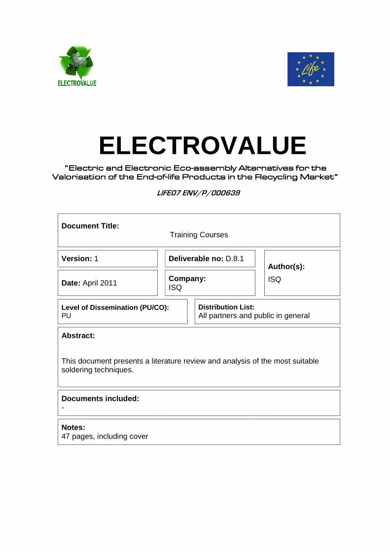
B. Prepare the soldering iron:
o Plug in iron to allow it to reach temperature.
o Dampen sponge
o Clean tip with sponge
Figure 12: Cleaning the tip of the soldering iron with a sponge (photo source: Clube do Hardware)
o Apply solder to iron tip (tinning)
o Wipe excess solder

D.8.1 – Training Courses
12
o Tip should be have silvery sheen
C. Execute (soldering)
D. Inspect solder joints:
o Inspection is undertaken to standard operating procedures.
o Inspection results are recorded /reported in accordance with work site
procedures:
i. Identification of both correct and incorrect soldering procedures and correct
and incorrect solder work.
ii. Understanding of codes, standards, manuals and manufacturers
specifications.
iii. Bond should be a cone and shiny.
iv. Profile of bond should be concave, not convex.
v. Bond surrounds part completely…. not 99%.
vi. Bond does not cover other connections.
o Repair bad joints.
o Remove solder bridges:
i. Excess solder connects two pads, leads.
ii. Unwanted electrical connection formed.
o Remove components.
o Both require old solder removal.

D.8.1 – Training Courses
13
2. DESOLDERING COMPONENTS
2.1. INTRODUCTION
Desolder components is not as easy as soldering them. Desoldering a component takes
about ten times more than soldering it. That’s why it should be done with careful and
takes one’s time when assembling boards. The main problem is that the PCB have
multiple layers. Only two layers (called "solder layer" and "component layer") are visible,
but there are other layers within the PCB, like a sandwich. The holes where the
components are welded metal and are used not only for the fit of components, but also
to provide electrical connection between the two visible layers and layers of the PCB,
which are not visible. If you make a wrong move while you are removing a component,
you can break the link between the hole and the inner layers of the board, destroying it.
2.2. TOOLS
To desolder components you will need the following tools:
• Soldering Iron It is advisable to use irons 25 W or 30 W, 40 W maximum if the solder is too old. Above
that can damage the circuit board components and even burn.
The soldering iron has a temperature control system, which automatically selects the
correct temperature solder based on the tip inserted into the soldering iron.
Figure 13: Soldering Iron
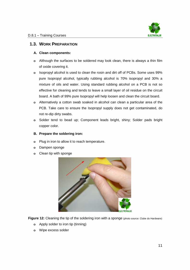
The most common soldering tip types are: a round conical fine point tip, and a flat edge
tip.
D.8.1 – Training Courses
14
Figure 14: Soldering tips types
• Desolder Wick
It is composed by braided copper strands which absorb the solder when heated. (You
should always remove excess solder.)
Figure 15: Desolder Wick
• Desolder pump
Used to heat and vacuum up old solder. The OKI unit has a built in vacuum pump and
filter cartridge. To clean the various desoldering tips an insertion tool can be used. When
the desoldering tool is hot insert the tool to clear any blocking solder balls.
Figure 16: Desoldering Pump
• Magnifier
The magnifier is an essential tool used for inspection and fine soldering work. As PCB
trouble shooting is about 70% visual inspection, the magnifier greatly assists this.
Alternatively a photo can be taken and amplified up on the computer to do visual
inspections.

D.8.1 – Training Courses
15
Figure 17: Magnifier
• Heat sink
The Heat sink is a clip between body and iron, which protects heat sensitive
components.
• Weld
• Cleaning Cloth
• Sponge
• Small screwdriver
• Isopropyl alcohol (Isopropanol)
• Brush
Figure 18: Necessary tools for desoldering (photo source: Clube do Hardware)
2.3. DESOLDERING PROCESS
Step 1: Preparation Work
Connect your soldering iron and wait until it heats up (three minutes on average). Wet
the sponge and wipe the tip of the soldering iron, making the movement shown in figure.

D.8.1 – Training Courses
16
Make sure to repeat the movement to the edge of the iron. It is normal that during the
process of cleaning out the smoke of iron, since the sponge is wet.
Figure 19: Cleaning the tip of the soldering iron with a sponge (photo source: Clube do Hardware)
During the desoldering process you need to clean the tip of the soldering iron again.
Whenever you notice that the tip of the soldering iron is dirty, repeat the cleaning
process shown above.
Step 2: Location of Component Terminals
The next step is to look carefully at the component you want to remove. As stated
above, the PCB has two visible sides, the side where the components are located, and
the solder side, where components are soldered. Therefore, it is necessary to locate the
component on the component side and seek their terminals in the solder side.
As an example we use an electrolytic capacitor of a board as shown in next figure.

D.8.1 – Training Courses
17
Figure 20: Location of electrolytic capacitor on components side (photo source: Clube do
Hardware)
Figure 21: Searching for component terminals (photo source: Clube do Hardware)

D.8.1 – Training Courses
18
Figure 22: Location of electrolytic capacitor terminals on solder side (photo source: Clube do
Hardware)
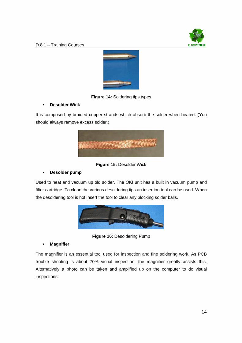
Step 3: Clean the component terminals
After locating the component terminals is necessary to clean them with isopropyl alcohol
(aka isopropanol) using a toothbrush. To do this, wet the toothbrush with isopropyl
alcohol and "brush" terminals. Do not use rubbing alcohol.
Figure 23: Wetting the toothbrush with isopropyl alcohol (photo source: Clube do Hardware)
D.8.1 – Training Courses
19
Figure 24: Cleaning the terminals of the component. (photo source: Clube do Hardware)
Figure 25: Terminals cleaned properly (photo source: Clube do Hardware)
Step 4: Preparing for Desolder
During this step the component to be removed will need to be weld again to allow the old
solder to be removed. The old solder is very difficult to be melted with the soldering iron
and sucked by the sucker, so it is necessary to mix fresh solder with solder old. This
mixture makes it easier to melt the solder and consequently to be removed.
There is an additional process to be carried out during this step. With the tip of the
soldering iron, push the terminal back and forth to make him fall off the edge of the hole.
In some situations the terminals are stuck on the edge which makes the removal
process very difficult. You should repeat this process at least twice in each direction.

D.8.1 – Training Courses
20
After this process the component terminal should be more or less in the middle of the
hole.
Figure 26: Soldering one terminal (photo source: Clube do Hardware)
Figure 27: Soldering another terminal (photo source: Clube do Hardware)

D.8.1 – Training Courses
21
Figure 28: Pushing forward the terminal with the soldering iron tip (photo source: Clube do
Hardware)
Figure 29: Pushing back the terminal with the soldering iron tip (photo source: Clube do
Hardware)
Step 5: Desolder the component
To desolder the component you will need a solder sucker. You should arm it, placing the
trigger down. To use it, you must press the button (trigger): it will drive back to the
original position sucking everything is located near its tip.
With one hand, you should melt the solder located in the terminal component and, with
the other, you should hold the solder sucker, positioning its tip in the molten solder and
press your button. The molten solder should be sucked.

D.8.1 – Training Courses
22
Tip: Never let your solder sucker armed after the work has been done. This will cause it
to lose its pressure.
Figure 30: Solder sucker. Trigger it with your thumb (photo source: Clube do Hardware)
Figure 31: Correct way to hold the solder sucker to use it (photo source: Clube do Hardware)
You should pay close attention to how the soldering iron must be handled, as shown in
next figure.

D.8.1 – Training Courses
23
Figure 32: Correct way to hold the soldering iron (photo source: Clube do Hardware)
Figure 33: Desoldering the component (photo source: Clube do Hardware)
Step 6: Repeating the process
It is very rare to remove all the solder on the first try. You need to repeat the process.
You may need to solder the component back to mixing the new with the old solder,
making it easier to melt the solder and suction. Another tip is to move the terminal to
back and front with the help of a small screwdriver to detach it from the hole.

D.8.1 – Training Courses
24
Figure 34: Terminals after the first desoldering (photo source: Clube do Hardware)
Figure 35: Pushing the terminal forward with a small screwdriver (photo source: Clube do
Hardware)
D.8.1 – Training Courses
25
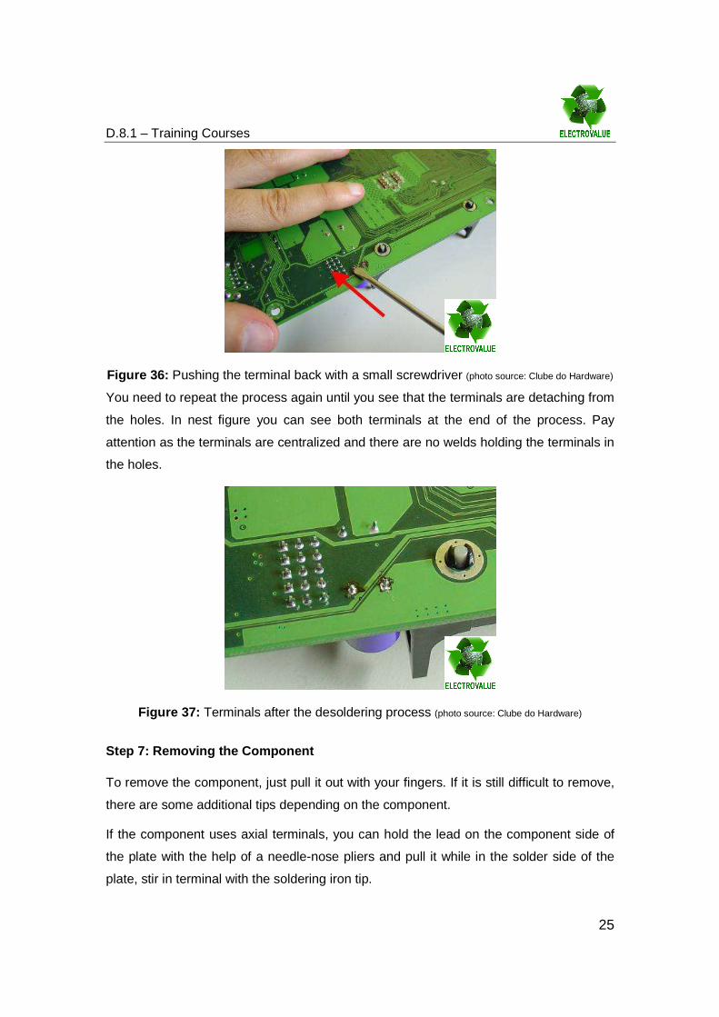
Figure 36: Pushing the terminal back with a small screwdriver (photo source: Clube do Hardware)
You need to repeat the process again until you see that the terminals are detaching from
the holes. In nest figure you can see both terminals at the end of the process. Pay
attention as the terminals are centralized and there are no welds holding the terminals in
the holes.
Figure 37: Terminals after the desoldering process (photo source: Clube do Hardware)
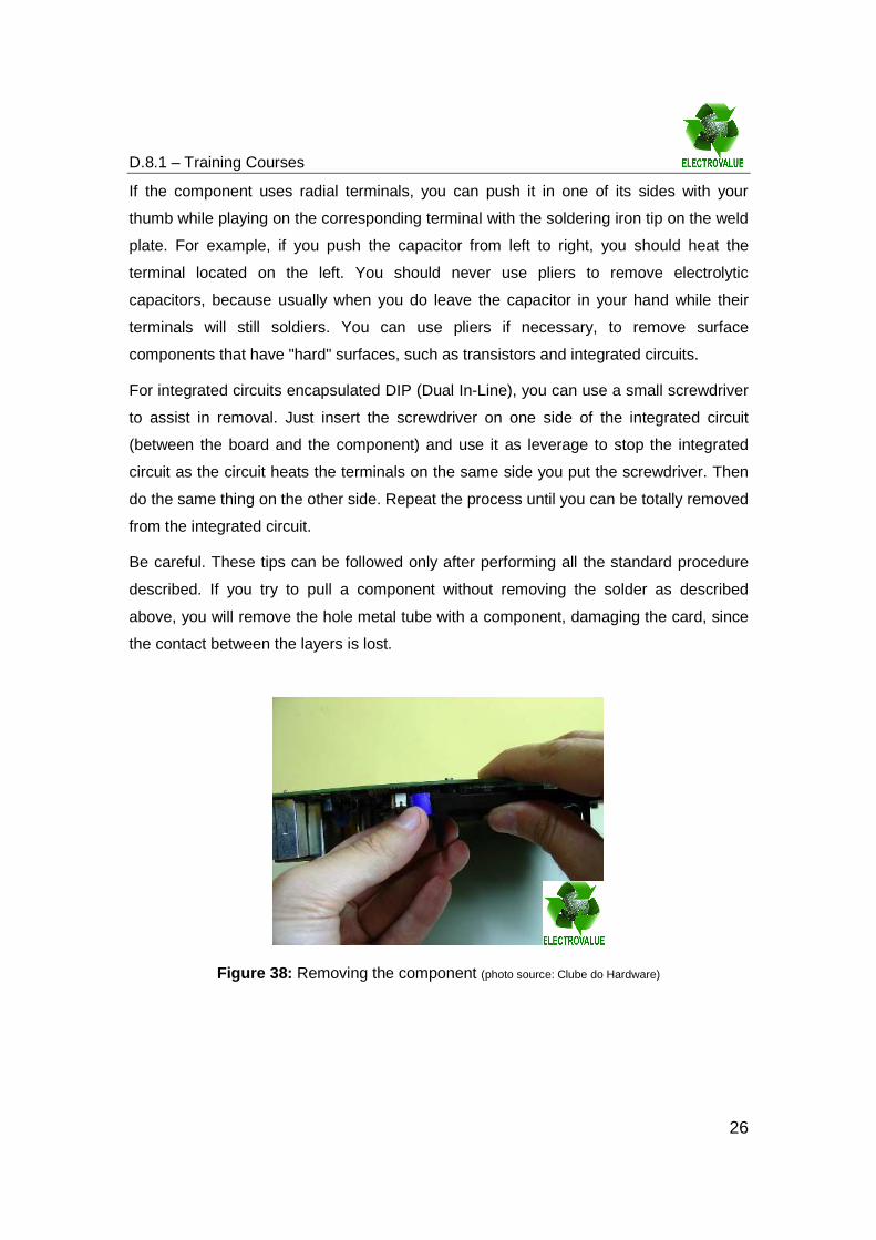
Step 7: Removing the Component
To remove the component, just pull it out with your fingers. If it is still difficult to remove,
there are some additional tips depending on the component.
If the component uses axial terminals, you can hold the lead on the component side of
the plate with the help of a needle-nose pliers and pull it while in the solder side of the
plate, stir in terminal with the soldering iron tip.
D.8.1 – Training Courses
26
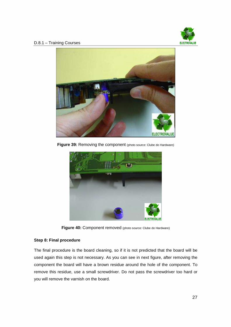
If the component uses radial terminals, you can push it in one of its sides with your
thumb while playing on the corresponding terminal with the soldering iron tip on the weld
plate. For example, if you push the capacitor from left to right, you should heat the
terminal located on the left. You should never use pliers to remove electrolytic
capacitors, because usually when you do leave the capacitor in your hand while their
terminals will still soldiers. You can use pliers if necessary, to remove surface
components that have "hard" surfaces, such as transistors and integrated circuits.
For integrated circuits encapsulated DIP (Dual In-Line), you can use a small screwdriver
to assist in removal. Just insert the screwdriver on one side of the integrated circuit
(between the board and the component) and use it as leverage to stop the integrated
circuit as the circuit heats the terminals on the same side you put the screwdriver. Then
do the same thing on the other side. Repeat the process until you can be totally removed
from the integrated circuit.
Be careful. These tips can be followed only after performing all the standard procedure
described. If you try to pull a component without removing the solder as described
above, you will remove the hole metal tube with a component, damaging the card, since
the contact between the layers is lost.
Figure 38: Removing the component (photo source: Clube do Hardware)
D.8.1 – Training Courses
27
Figure 39: Removing the component (photo source: Clube do Hardware)
Figure 40: Component removed (photo source: Clube do Hardware)
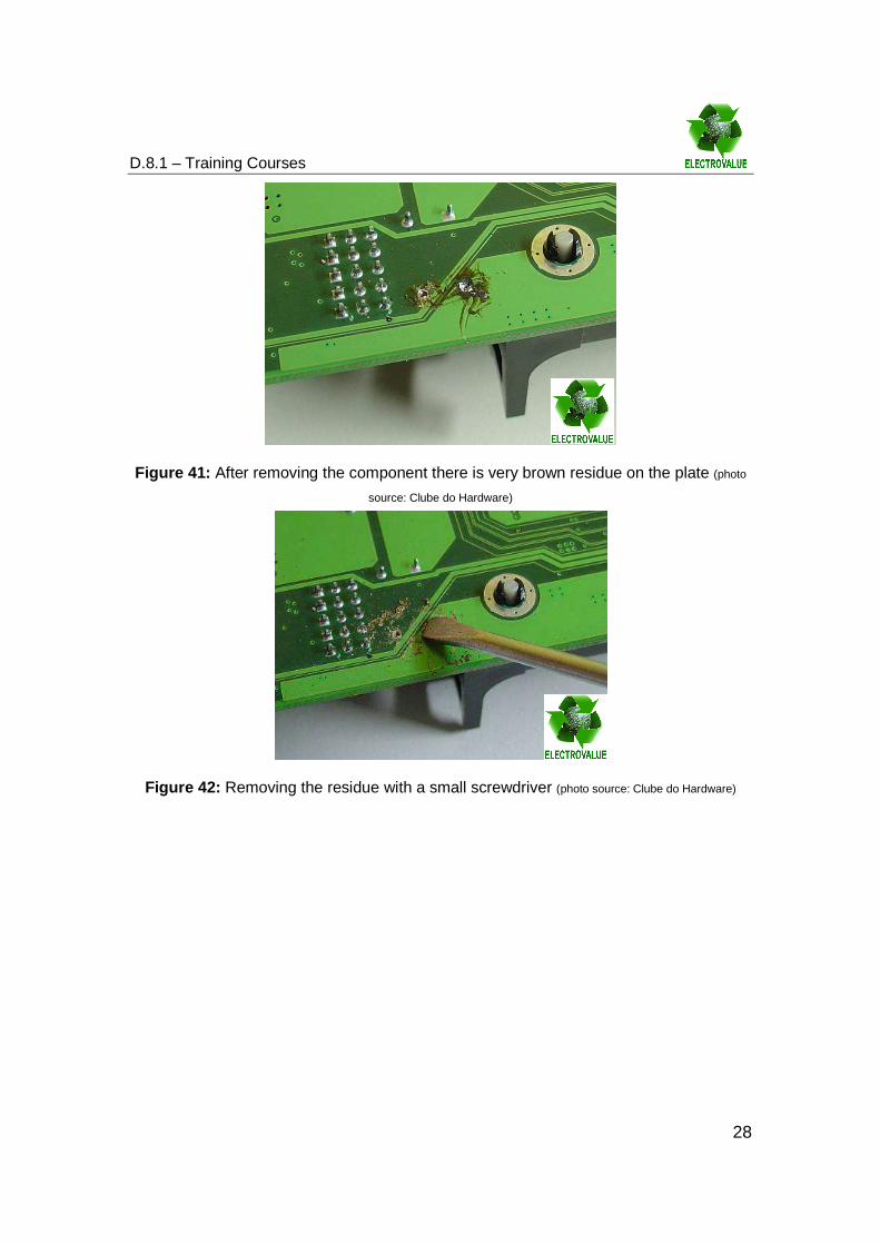
Step 8: Final procedure
The final procedure is the board cleaning, so if it is not predicted that the board will be
used again this step is not necessary. As you can see in next figure, after removing the
component the board will have a brown residue around the hole of the component. To
remove this residue, use a small screwdriver. Do not pass the screwdriver too hard or
you will remove the varnish on the board.
D.8.1 – Training Courses
28
Figure 41: After removing the component there is very brown residue on the plate (photo
source: Clube do Hardware)
Figure 42: Removing the residue with a small screwdriver (photo source: Clube do Hardware)
D.8.1 – Training Courses
29
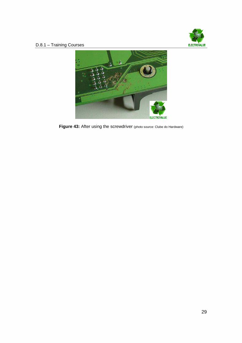
Figure 43: After using the screwdriver (photo source: Clube do Hardware)

D.8.1 – Training Courses
30
2.4. DESOLDERING T ECHNIQUES
A. Desoldering Pumps
1. To use a desoldering pump, first load the pump by depressing the plunger until
it latches.
Figure 44: Desoldering Pump
2. Grasp the pump in one hand and the soldering iron the other, and apply heat to
the bad joint. When the solder melts, quickly remove the soldering iron and
bring in the pump in one continuous motion.
3. Trigger the pump to suck up the solder while it is still molten.
Figura 45: Desoldering using a desoldering pump (photo source: Clube do Hardware)
B. Desoldering Wick
� Charge the “Solder Sucker”.
� Place the tip of the iron on the joint to be desoldered.
� Once the solder on the joint liquefies, insert the tip of the “Solder Sucker” into the
molten solder and trigger it.
� Use “Solder Wick” to remove the last residue of solder.
� Use a screw driver & long nose pliers to help remove the component.

D.8.1 – Training Courses
31
Figure 46: Desoldering using a desoldering wick
C. Heatgun Desoldering
Step 1: Remove the PCB from any other casings. You can use just a few screws to
remove.
Step 2: Heat up area using heat gun. Use something non flammable to put the item on
and place it at a comfortable angle to work with. Make sure there is nothing that could
melt or burn in the area around it. Heat the area around the yellow SMT parts in the top
left corner, after heating the area. Watch the solder to turn shiny to show that it’s flowing.
You can then remove the parts using tweezers or needle nose pliers. Then place in a
safe place to cool off.
Step 3: Be careful especially with the smaller parts or the parts that might be heat
sensitive. The air from the heat gun can blow small parts around. You also don't want to
burnout the parts you are trying to save.
D.8.1 – Training Courses
32
2.5. TIPS
General Desoldering Advice
o Adding additional solder to a troublesome joint can be helpful in removing the last
traces of solder. This works because the additional solder helps the heat to flow
fully into the joint. The additional solder should be applied and de-soldered as
quickly as possible. Don’t wait for the solder to cool off before attempting to suck
it away.
o Desoldering works effectively when the joint is hot, and there is ample solder to
be removed. Additional solder can be added to joints that are difficult to desolder.
The additional solder transfers heat to the existing solder, allowing it to be de-
soldered more easily.
o Use heatsinks. Heatsinks are a must for the leads of sensitive components such
as ICs and transistors. If you don't have a clip on heatsink, then a pair of pliers is
a good substitute.
o Keep the iron tip clean. A clean iron tip means better heat conduction. Use a wet
sponge to clean the tip between joints.
o Check the pads. Use a continuity tester to check to make sure you did not
damage the pad or trace when you removed the solder. If you did, then follow the
steps above to fix it.
o Use the proper iron. Remember that bigger joints will take longer to heat up with
a 30W iron than with a 150W iron. While 30W is good for PCB and the like,
higher wattages are great when desoldering heavy connections, such as those to
a chassis.
o Use both a solder sucker and solder wick. Use a solder sucker to remove the
majority of the solder and then follow up with the wick to finish things up.
o Whenever you see the tip of a soldering iron with black sections should clean it.

D.8.1 – Training Courses
33
3. COMPONENTS
A. Resistors
Resistors are small cylindrical devices with color-coded bands indicating their value.
B. Resistor Packs
Resistor packs are flat, rectangular packages with anywhere from six to ten leads. There
are two basic types of resistor pack:
- Isolated Element. Discrete resistors: usually three, four, or five per package.
- Common Terminal. Resistors with one pin tied together and the other pin free.
C. Diodes
Diodes have two leads, called the anode and cathode. A diode package usually provides
a marking that is closer to one lead than the other (a band around a cylindrical package,
for example). This marked lead is always the cathode.
Figure 47: Typical diode package
D. LEDs
LED is an acronym for “light emitting diode” so it should not come as a surprise that
LEDs are diodes too. An LED’s cathode is marked either by a small flat edge along the
circumference of the diode casing, or the shorter of two leads.
Figure 48: LED

D.8.1 – Training Courses
34
E. Integrated Circuits
Integrated circuits (ICs) come in a variety of package styles. Two common types are
called the DIP (for dual-inline package), and the PLCC (for plastic leaded chip carrier). In
both types a marking on the component package signifies “pin 1” of the component’s
circuit. This marking may be a small dot, notch, or ridge in the package. After pin 1 is
identified, pin numbering proceeds sequentially in a counter-clockwise fashion around
the chip package.
Figure 49: Top view of 14-pin DIP
F. Capacitors
Quite a few different kinds of capacitors are made each having different properties. As
indicated, some capacitors are non-polarized while other types are polarized. It’s
important to mount polarized capacitors correctly. All polarized capacitor placements are
marked with a plus symbol (+) and a minus symbol (-). The pads on the boards are also
marked differently. The negative lead (-) goes through a square hole and the positive
lead (+) goes through the round hole.
The capacitors themselves are sometimes obviously marked and sometimes are not.
One or both of the positive or negative leads may be marked, using (+) and (-) symbols.
In this case, install the lead marked (+) in the hole marked (+).
Some capacitors may not be marked with (+) and (-) symbols. In this case, one lead will
be marked with a dot or with a vertical bar. This lead will be the positive (+) lead.
G. Inductors
Some inductors are coated with epoxy and look quite like resistors. Others are big bulky
coils with iron cores. Inductors are not polarized.
H. Transistors
Transistors are polarized devices and for larger currents larger the transistor are used.
D.8.1 – Training Courses
35
I. Relays
A relay is an electrically operated switch. Many relays use an electromagnet to operate a
switching mechanism mechanically, but other operating principles are also used. Relays
are used where it is necessary to control a circuit by a low-power signal (with complete
electrical isolation between control and controlled circuits), or where several circuits
must be controlled by one signal.
J. Fuses
A fuse is a type of sacrificial overcurrent protection device. Its essential component is a
metal wire or strip that melts when too much current flows, which interrupts the circuit in
which it is connected. Short circuit, overload or device failure is often the reason for
excessive current.
A fuse interrupts excessive current (blows) so that further damage by overheating or fire
is prevented. Wiring regulations often define a maximum fuse current rating for particular
circuits. Overcurrent protection devices are essential in electrical systems to limit threats
to human life and property damage. Fuses are selected to allow passage of normal
current and of excessive current only for short periods.

D.8.1 – Training Courses
36
4. SAFETY
4.1. FIRST AID
If you are unlucky enough to receive burns which require treatment, here's what to do:
� Immediately cool the affected area with cold running water for several minutes.
� Remove any rings etc. before swelling starts.
� Apply a sterile dressing to protect against infection.
� Do not apply lotions, ointments etc., nor prick any blisters which form later.
� Seek professional medical advice where necessary.
4.2. SECURITY @ WORK
� Keep your workstation clean and organized. Food or drinks, or products for
personal use are not allowed.
� Handling of PCB should be kept to a minimum. The use of gloves is always
preferred and required in some circumstances.
� As a general rule, metallized surfaces which will be solder after or electrical
contacts of the product (eg carbon pads or gold plated) never in any
circumstance should be played with free hands (gloves are required).
� Never stack PCB, as this represents a huge risk of broken components. Always
use the appropriate magazines.
� Do not lick, bite or place hands in mouth.
� Do not hold solder for excessive periods of time.
� Avoid breathing fume, guaranteed it’s not nicotine!
� Wash your hands before leaving the lab each day.
� Always be careful, you are working with extreme heat.
� Soldering irons melt metal.
� They get very hot and can start fires.
� Never leave a soldering iron unattended.

D.8.1 – Training Courses
37
� Well lighted work area.
� Use safety glasses.
� Keep the soldering iron tips away from everything except the point to be
soldered. Keep the soldering iron in its holder when it is not being held.
� Do not hold the iron against the joint for an extended period of time (more than 6
seconds), since many electronic components or the PCB itself can be damaged
by prolonged, excessive heat.
4.2.1. CONTAMINATION
The handling of cards without gloves can cause future problems of welding. The fat
acids and elements of our sweat, are aggressive to make the plates and start the
oxidation processes that severely undermined the weldability of the panels.
4.2.2. HANDLING OF ELECTRONIC CIRCUITS
Avoid contaminating solderable surfaces prior to welding. Any material that is in contact
with these surfaces must be clean. The plates are quite sensitive to handling, particularly
mechanical impact. Be aware that you are handling a sensitive product.
4.2.3. GLOVES AND VINGERCOTS
The use of gloves and vingercots is required when handling a card that will still be
subject to a welding process. If you do not have gloves handle the card if you do so only
by the edges without touching the areas to be welded.
D.8.1 – Training Courses
38
5. GLOSSARY
Acid: A hydrogen-containing substance which breaks down upon solution in water to
produce hydrogen ions. Acid strength is determined by the quantity of hydrogen irons
which are released into the solution. The higher the concentration of hydrogen, the
stronger the acid.
Activated: The condition of a compound or mixture of compounds having higher
chemical activity than that normally found with the compound or mixture. An example is
the addition of an activator to rosin to increase fluxing activity.
Alloy: A combination of two or more metal elements. An example is 63% tin plus 37%
lead, a solder alloy.
Anti-static protection: If you're interested in soldering a lot of static-sensitive parts (e.g.
CMOS chips or MOSFET transistors), more advanced and expensive soldering iron
stations use static-dissipative materials in their construction to ensure that static does
not build up on the iron itself.
Auto Ignition Point: The temperature at which vapour from a material in air will
spontaneously burst into flame.
Bits: It's useful to have a small selection of manufacturer's bits (soldering iron tips)
available with different diameters or shapes, which can be changed depending on the
type of work in hand. Often, tips are iron-coated to preserve their life, or they may be
bright-plated instead.
Boiling Point: The temperature of a liquid at which its vapour pressure is equal to the
pressure of the atmosphere surrounding the fluid.
Bonding Pad: A metalized area at the end of a thin metal strip or on a semiconductor to
which the connection is made.
Brazing: A group of joining processes wherein the filler metal is a non ferrous metal or
alloy whose melting point is typical higher than 1000°F but lower than that of the metals
or alloys to be joined. At one extreme, brazing is similar to soldering and is sometimes
called hard soldering.
D.8.1 – Training Courses
39
Burnoff: Removal of electroless copper as a result of excessive current. Usually occurs
at edges of holes and causes plating failure in the hole.
Capillary Action: The interaction between a liquid and a small diameter channel or
opening in a solid. Because of the physics involved, if the liquid wets the sides of the
solid channel, surface tension will draw the liquid up into the capillary channel.
Cathode: The negative pole of a plating cell. It is the physical entity of the plating set-up
at which positively charged ions leave the plating solution. The cathode is normally the
object of the plating, i.e. a metal is deposited on the cathode.
Chemical Stability: That characteristic of a compound which describes its ability to
retain, without modification, its chemical properties over a long period of time.
Circuit: The interconnection of a number of devices in one or more closed paths to
perform a desired electrical or electronic function.
Cold Solder Joint: Incorrectly made solder joint caused either by a soldering iron with
too low a tip temperature or by heating of the solder rather than the metals to be joined.
Component: Any part placed on a printed circuit assembly i.e. resistor, capacitor, diode.
Compound: A homogenous pure substance composed of two or more essentially
different chemical elements, which are present in definite proportions.
Contaminant: An impurity or foreign substance present in a material or on a surface
which affects performance in the material or circuit.
Corrosion: The most common kind of corrosion is that of rusting. This is known as
atmospheric corrosion wherein the oxygen of the atmosphere reacts with the material in
question. Most metals with the exception of the noble metals such as gold, can be
oxidized by atmospheric oxygen.
Creep Strength: A characteristic of a material which describes its strength and
resistance to elongation i.e. stretching at low loads. This characteristic can be measured
either as the load to fracture the sample at a given temperature, or the load that will
produce a given percent of stretch, or elongation, at a given temperature.
Desoldering: Remove the solder from a connection without damaging the component or
the PCB (wire or the terminal).

D.8.1 – Training Courses
40
Dewetting: A condition which results when molten solder has coated a surface and then
receded, leaving irregularly shaped mounds of solder separated by areas covered with a
thin solder film, base metal is not exposed.
Dip Soldering: The process of soldering all components on a board at one time by
dipping the board in a solder pot. The board is not dipped deeply enough to immerse
components.
Dross: Metal oxides and other entrapped impurities which float in or on the surface of a
molten metal bath. In the case of solder, it would include the oxides of lead and tin, in
addition to non-metallic impurities such as flux residues that were dragged into the
solder bath, and oxides of any metal impurities found in the solder.
Element: A substance which cannot be decomposed or otherwise modified by ordinary
types of chemical processes. Neither can an element be made by chemical union.
Eutectic: When applied to an alloy, eutectic refers to the composition of an alloy which
has the lowest melting pint of a series. For example in the tin/lead system, Sn63/PB37 is
the eutectic. This is the alloy composition of all those in the Sn/Pb system which has the
lowest liquidus.
Evaporation: A physical process by which a liquid loses material to the atmosphere
surrounding it. Evaporation is caused by the motion of the molecules of the liquid.
Flash Point: Temperature at which a volatile liquid mixes with air in such proportions as
to produce flammable gaseous mixture. The mixture will flash when exposed to a flame
or spark but will not necessarily continue to support combustion.
Flux: As used in soldering, i.e. a material which cleans metal surfaces of absorbed
gases, oxide films and other tarnishes. The flux also reduces the surface tension of the
molten solder and the metal to be soldering, so that the solder may flow and wet the
metal surface.
Freezing Point: The temperature at which a previously molten material solidifies, or
becomes completely solid.
Hot Air Levelling: Process used in solder dipping of bare copper circuitry in which high
velocity air is used to blow solder clear from plated through holes and to minimize solder
thicknesses.

D.8.1 – Training Courses
41
Icicling: The formation of solder spikes resulting from poor drain off of liquid solder
following wave or dip soldering of printed circuit boards and assemblies. Poor
solderability of the surfaces to be soldered and contaminated solder is frequent causes
of icicling.
Inorganic: When applied to chemistry, refers to the chemistry of those compounds
found in nature or synthesized by man which do not depend essentially upon chemistry
of carbon for their properties.
Junction: A joining of two different semiconductors or of semiconductor and a metal.
Leakage: Loss of insulation between conductors on a board. May be due to improper
cleaning procedures that leave conductive residues.
Liquidus: The temperature at which an alloy is completely molten.
Metallurgy: The area concerned with the extraction of metals for their orders and the
refiring of these metals is known as the process of metallurgy.
Molecule: The smallest quantity of matter which can exist by itself and be recognizable
as a particle of the original material. A molecule retains all the properties of the bulk
substance from which it came.
Organic Halides: An organic compound containing halogens.
Pad: Area of copper surrounding a hole in a board to be used for lead of component, or
for insertion of interconnecting wire. Provides area for solder bonding.
PCB: A printed circuit board, at almost any stage in production from raw material to the
finished assembly complete with components.
Pick and Place Equipment: The automated pick up and placement of discrete active
and passive devices on ceramic substrates.
Plastic Range: Refers to a range of temperature in which metal or alloy can be
mechanically worked without danger or cracking of the material.
Polarity: It refers to the concept that many electronic components are not symmetric
electrically. A polarized device has a right way and a wrong way to be mounted.
Polarized components that are mounted backwards will not work, and in some cases will
be damaged or may damage other parts of the circuit.

D.8.1 – Training Courses
42
Reflow Soldering: A method in which a solder joint is made by melting the solder
coatings on them mating surfaces.
Resin: A solid or semi solid organic compound lacking a crystalline structure. Resins are
characterised by not having definite and sharp melting points, are not usually conductors
of electricity.
Rosin: A naturally occurring resin usually associated as a components of pine sap.
Rosin alone is a mild flux for soldering operations.
Shelf Life: Length of time under specified conditions that a stored material in original,
unopened containers retains usability.
Solder: A metal or metal alloy usually having a low melting point, used to join other
metals having higher melting points than the solder together.
Solder Paste: Homogenous combinations of solder and flux, solvent and gelling or
suspension agent for automated production of solder joints.
Solder Preforms: Manufactured solder configurations containing a predetermined
quantity of alloy, with or without a flux core or coating.
Solder Resists: Coatings which mask off a surface which insulate those areas of a
circuit where soldering is not desired.
Solidus: The temperature at which a metal alloy begins to melt
Spare parts: it's nice to know that spare parts may be available, so if the element blows,
you don't need to replace the entire iron. This is especially so with expensive irons.
Check through some of the larger mail-order catalogues.
Soldering: to join two metals together to form an electrically mechanically secure bond
using heat and a third metal alloy known as solder.
Solder: a metal alloy of tin and lead (60/40) with a low melting point of 187°C & rosin
core.
Specific Gravity: The ratio of the density of a material to the density of water.
Surface Mount Devices: Electronic components, either active or passive which do not
have separate leads. The terminal leads are part of the component body, allowing direct
mounting on the surface of the printed wiring boards

D.8.1 – Training Courses
43
Temperature Control: the simplest and cheapest types don't have any form of
temperature regulation. Simply plug them in and switch them on! Thermal regulation is
"designed in" (by physics, not electronics!): they may be described as "thermally
balanced" so that they have some degree of temperature "matching" but their output will
otherwise not be controlled. Unregulated irons form an ideal general purpose iron for
most users, and they generally cope well with PCB soldering and general interwiring.
Tensile Strength: The characteristic of a material which describes its resistance to
fracture when the material is being stretched. I.e. Under a tensile load.
Thixotropic: The characteristic of a liquid or gel that is viscous when static, yet fluid
when physically worked.
Tinning: Coating of a terminal, lead or conductive pattern with tin or solder alloy to
improve maintain solderability or to aid in the soldering operation.
Viscosity: The measure of resistance of a fluid to flow- though a specific orifice or in a
rotational viscometer.
Volatile: Used to describe materials which have a relatively high evaporation rate or a
tendency to evaporate
Voltage: most irons run from the mains at 240V. However, low voltage types (e.g. 12V
or 24V) generally form part of a "soldering station" and are designed to be used with a
special controller made by the same manufacturer.
Water Based: A description of a liquidus system where the primary solvent is water
Wattage: Typically, they may have a power rating of between 15-25 watts or so, which is
fine for most work. A higher wattage does not mean that the iron runs hotter - it simply
means that there is more power in reserve for coping with larger joints. This also
depends partly on the design of the "bit" (the tip of the iron). Consider a higher wattage
iron simply as being more "unstoppable" when it comes to heavier-duty work, because it
won't cool down so quickly.
Wave Soldering: The technique of soldering components to a board by passing the
board over a wave of solder in a soldering pot. The wave is maintained above the level
of the pot by solder being pumped through a manifold in the bottom of the pot.

D.8.1 – Training Courses
44
Wetting: A physical phenomenon of liquids usually in contact with solids, whereas the
surface tension of the liquid has been reduced so that the liquid flows and makes
intimate contact in a very thin layer over the entire substrate surface.

D.8.1 – Training Courses
45
6. REFERENCES
http://www.solderandsoldering.co.uk/pages/Glossary.html
Top Related