


Languages
Pages
Legal


EFM32 Jade Gecko FamilyEFM32JG1 Data Sheet
The EFM32 Jade Gecko MCUs are the world’s most energy-friendly microcontrollers.
EFM32JG1 features a powerful 32-bit ARM® Cortex®-M3 and a wide selection of periph-erals, including a unique cryptographic hardware engine supporting AES, ECC, andSHA. These features, combined with ultra-low current active mode and short wake-uptime from energy-saving modes, make EFM32JG1 microcontrollers well suited for anybattery-powered application, as well as other systems requiring high performance andlow-energy consumption.
Example applications:
ENERGY FRIENDLY FEATURES
• ARM Cortex-M3 at 40 MHz• Ultra low energy operation:
• 2.1 μA EM3 Stop current (CRYOTIMERrunning with state/RAM retention)
• 2.5 μA EM2 DeepSleep current (RTCCrunning with state and RAM retention)
• 63 μA/MHz in Energy Mode 0 (EM0)• Hardware cryptographic engine supports
AES, ECC, and SHA• Integrated dc-dc converter• CRYOTIMER operates down to EM4• 5 V tolerant I/O
• IoT devices and sensors• Health and fitness• Smart accessories
• Home automation and security• Industrial and factory automation
Peripheral Reflex System
32-bit bus
Core / Memory
Lowest power mode with peripheral operational:
EM2 – Deep SleepEM1 - Sleep EM4 - Hibernate EM4 - ShutoffEM0 - Active EM3 - Stop
Serial Interfaces
USART
Low Energy UARTTM
I2C
I/O Ports Timers and Triggers
CRYOTIMER
Real Time Counter and Calendar
Other
CRYPTO
CRC
Analog Interfaces
ADC
IDAC
Analog Comparator
Timer/Counter Low Energy Timer
Pulse Counter
Watchdog Timer
External Interrupts
General Purpose I/O
Pin Reset
Pin Wakeup
Flash Program Memory RAM Memory
ARM CortexTM M3 processor
Debug Interface DMA Controller
Energy Management
Brown-Out Detector
DC-DC Converter
Voltage Regulator Voltage Monitor
Power-On Reset
Clock Management
Low Frequency Crystal
Oscillator
High FrequencyRC Oscillator
Ultra Low Frequency RC
Oscillator
Auxiliary High Frequency RC
Oscillator
Memory Protection Unit
High Frequency Crystal
Oscillator
Low FrequencyRC Oscillator
silabs.com | Smart. Connected. Energy-friendly. Rev. 1.1

1. Feature List
The EFM32JG1 highlighted features are listed below.• ARM Cortex-M3 CPU platform
• High Performance 32-bit processor @ up to 40 MHz• Memory Protection Unit• Wake-up Interrupt Controller
• Flexible Energy Management System• 63 μA/MHz in Energy Mode 0 (EM0)• 2.5 μA EM2 DeepSleep current (RTCC running with state
and RAM retention)• 0.58 μA EM4H Hibernate Mode (128 byte RAM retention)
• Up to 256 kB flash program memory• 32 kB RAM data memory• Up to 32 General Purpose I/O Pins
• Configurable push-pull, open-drain, pull-up/down, input fil-ter, drive strength
• Configurable peripheral I/O locations• Asynchronous external interrupts• Output state retention and wake-up from Shutoff Mode
• Hardware Cryptography• AES 128/256-bit keys• ECC B/K163, B/K233, P192, P224, P256• SHA-1 and SHA-2 (SHA-224 and SHA-256)
• Timers/Counters• 2× 16-bit Timer/Counter
• 3 + 4 Compare/Capture/PWM channels• 1× 32-bit Real Time Counter and Calendar• 1× 32-bit Ultra Low Energy CRYOTIMER for periodic wake-
up from any Energy Mode• 16-bit Low Energy Timer for waveform generation• 16-bit Pulse Counter with asynchronous operation• Watchdog Timer with dedicated RC oscillator
• 8 Channel DMA Controller• 12 Channel Peripheral Reflex System (PRS) for autono-
mous inter-peripheral signaling• Communication Interfaces
• 2× Universal Synchronous/Asynchronous Receiver/ Trans-mitter• UART/SPI/SmartCard (ISO 7816)/IrDA/I2S/LIN• Triple buffered full/half-duplex operation with flow control
• Low Energy UART• Autonomous operation with DMA in Deep Sleep Mode
• I2C Interface with SMBus support• Address recognition in EM3 Stop Mode
• Ultra Low-Power Precision Analog Peripherals• 12-bit 1 Msamples/s Analog to Digital Converter• 2× Analog Comparator• Digital to Analog Current Converter• Up to 32 pins connected to analog channels (APORT)
shared between Analog Comparators, ADC, and IDAC• Ultra efficient Power-on Reset and Brown-Out Detector• Debug Interface
• 2-pin Serial Wire Debug interface• 1-pin Serial Wire Viewer• JTAG (programming only)
• Wide Operating Range• 1.85 V to 3.8 V single power supply• Integrated dc-dc, down to 1.8 V output with up to 200 mA
load current for system• Standard (-40 °C to 85 °C TAMB) and Extended (-40 °C to
125 °C TJ) temperature grades available• Packages
• 7 mm × 7 mm QFN48• 5 mm × 5 mm QFN32
• Pre-Programmed UART Bootloader• Full Software Support
• CMSIS register definitions• Low-power Hardware Abstraction Layer (HAL)• Portable software components• Third-party middleware• Free and available example code
EFM32JG1 Data SheetFeature List
silabs.com | Smart. Connected. Energy-friendly. Rev. 1.1 | 1
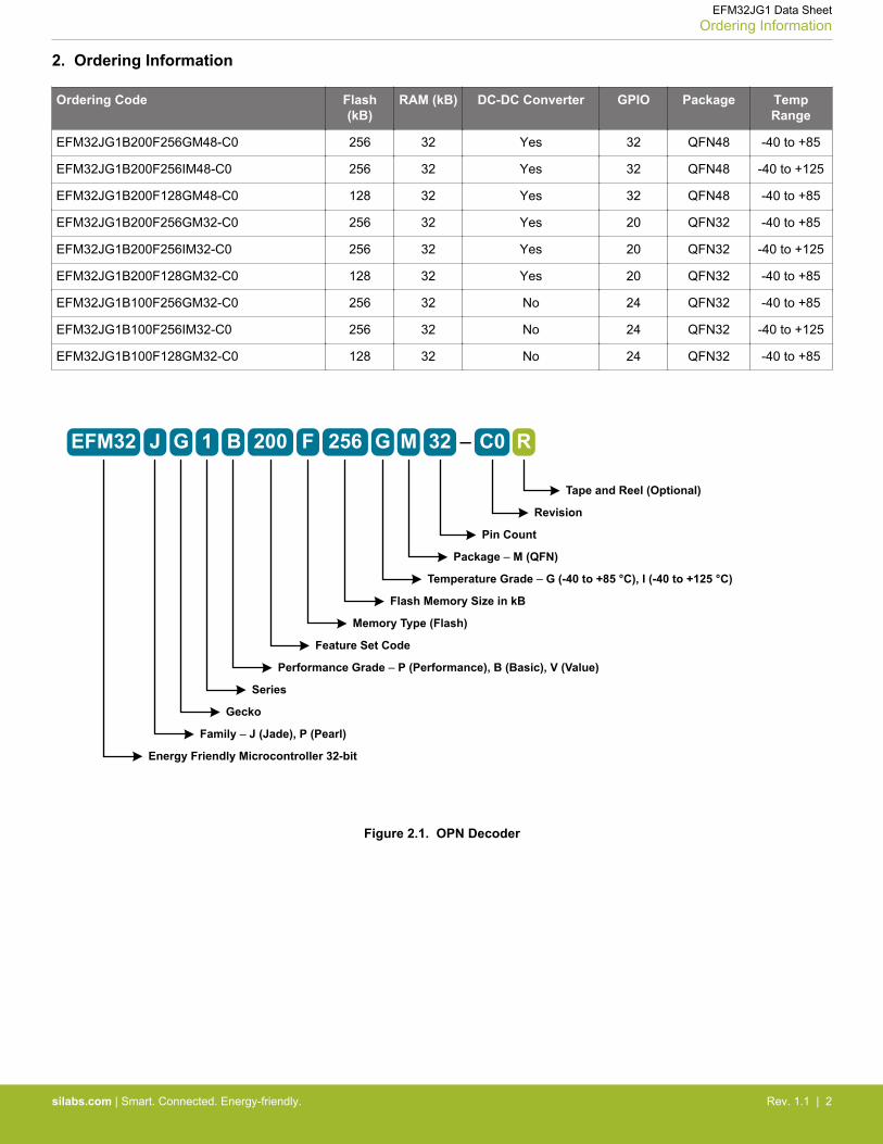
2. Ordering Information
Ordering Code Flash(kB)
RAM (kB) DC-DC Converter GPIO Package TempRange
EFM32JG1B200F256GM48-C0 256 32 Yes 32 QFN48 -40 to +85
EFM32JG1B200F256IM48-C0 256 32 Yes 32 QFN48 -40 to +125
EFM32JG1B200F128GM48-C0 128 32 Yes 32 QFN48 -40 to +85
EFM32JG1B200F256GM32-C0 256 32 Yes 20 QFN32 -40 to +85
EFM32JG1B200F256IM32-C0 256 32 Yes 20 QFN32 -40 to +125
EFM32JG1B200F128GM32-C0 128 32 Yes 20 QFN32 -40 to +85
EFM32JG1B100F256GM32-C0 256 32 No 24 QFN32 -40 to +85
EFM32JG1B100F256IM32-C0 256 32 No 24 QFN32 -40 to +125
EFM32JG1B100F128GM32-C0 128 32 No 24 QFN32 -40 to +85
EFM32 –1 B F G C0 R
Tape and Reel (Optional)
Revision
Pin Count
Package – M (QFN)
Flash Memory Size in kB
Memory Type (Flash)
Feature Set Code
GJ 200 256 M 32
Temperature Grade – G (-40 to +85 °C), I (-40 to +125 °C)
Performance Grade – P (Performance), B (Basic), V (Value)
Family – J (Jade), P (Pearl)
Series
Energy Friendly Microcontroller 32-bit
Gecko
Figure 2.1. OPN Decoder
EFM32JG1 Data SheetOrdering Information
silabs.com | Smart. Connected. Energy-friendly. Rev. 1.1 | 2
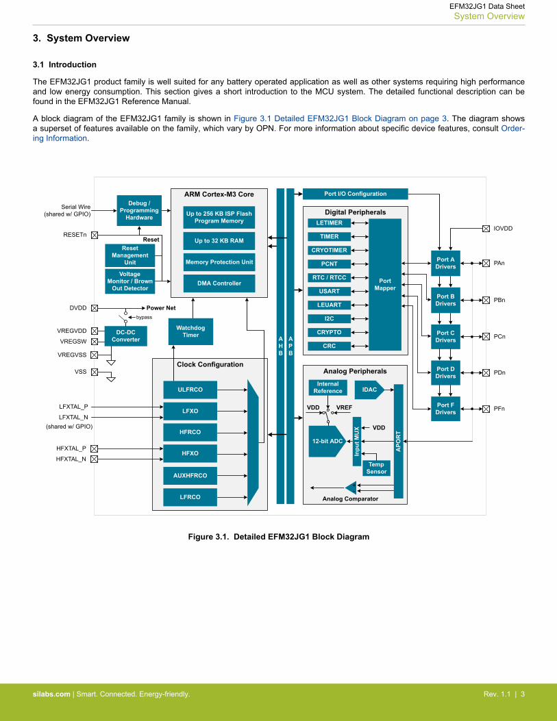
3. System Overview
3.1 Introduction
The EFM32JG1 product family is well suited for any battery operated application as well as other systems requiring high performanceand low energy consumption. This section gives a short introduction to the MCU system. The detailed functional description can befound in the EFM32JG1 Reference Manual.
A block diagram of the EFM32JG1 family is shown in Figure 3.1 Detailed EFM32JG1 Block Diagram on page 3. The diagram showsa superset of features available on the family, which vary by OPN. For more information about specific device features, consult Order-ing Information.
Analog PeripheralsClock Configuration
IDAC
ARM Cortex-M3 Core
Up to 256 KB ISP FlashProgram Memory
Up to 32 KB RAM
AHB
Watchdog Timer
Power Net
DC-DC Converter
DVDD
VREGVDD
VSS
Reset Management
Unit
Voltage Monitor / Brown
Out Detector
RESETnReset
Debug / Programming
HardwareDigital Peripherals
Inpu
t MU
X
Port Mapper
Port I/O Configuration
I2C
Analog Comparator
12-bit ADC
Temp Sensor
VREFVDD
VDD
Internal Reference
TIMER
CRYOTIMER
PCNT
USART
Port ADrivers
Port B Drivers
PAn
Port C Drivers PCn
PBn
Port D Drivers PDn
LETIMER
RTC / RTCC
IOVDD
AUXHFRCO
ULFRCO
VREGVSS
VREGSW
Port F Drivers PFn
Serial Wire(shared w/ GPIO)
Memory Protection Unit
LFRCO
APB
LEUART
CRYPTO
CRC
DMA Controller
+-
APO
RT
bypass
LFXTAL_P
LFXTAL_NLFXO
HFRCO
HFXOHFXTAL_P
HFXTAL_N
(shared w/ GPIO)
Figure 3.1. Detailed EFM32JG1 Block Diagram
EFM32JG1 Data SheetSystem Overview
silabs.com | Smart. Connected. Energy-friendly. Rev. 1.1 | 3

3.2 Power
The EFM32JG1 has an Energy Management Unit (EMU) and efficient integrated regulators to generate internal supply voltages. Only asingle external supply voltage is required, from which all internal voltages are created. An optional integrated dc-dc buck regulator canbe utilized to further reduce the current consumption. The dc-dc regulator requires one external inductor and one external capacitor.
AVDD and VREGVDD need to be 1.85 V or higher for the MCU to operate across all conditions; however the rest of the system willoperate down to 1.62 V, including the digital supply and I/O. This means that the device is fully compatible with 1.8 V components.Running from a sufficiently high supply, the device can use the dc-dc to regulate voltage not only for itself, but also for other PCB com-ponents, supplying up to a total of 200 mA.
3.2.1 Energy Management Unit (EMU)
The Energy Management Unit manages transitions of energy modes in the device. Each energy mode defines which peripherals andfeatures are available and the amount of current the device consumes. The EMU can also be used to turn off the power to unused RAMblocks, and it contains control registers for the DC-DC regulator and the Voltage Monitor (VMON). The VMON is used to monitor multi-ple supply voltages. It has multiple channels which can be programmed individually by the user to determine if a sensed supply hasfallen below a chosen threshold.
3.2.2 DC-DC Converter
The DC-DC buck converter covers a wide range of load currents and provides up to 90% efficiency in energy modes EM0, EM1, EM2and EM3, and can supply up to 200 mA to the device and surrounding PCB components. Protection features include programmablecurrent limiting, short-circuit protection, and dead-time protection. The DC-DC converter may also enter bypass mode when the inputvoltage is too low for efficient operation. In bypass mode, the DC-DC input supply is internally connected directly to its output through alow resistance switch. Bypass mode also supports in-rush current limiting to prevent input supply voltage droops due to excessive out-put current transients.
3.3 General Purpose Input/Output (GPIO)
EFM32JG1 has up to 32 General Purpose Input/Output pins. Each GPIO pin can be individually configured as either an output or input.More advanced configurations including open-drain, open-source, and glitch-filtering can be configured for each individual GPIO pin.The GPIO pins can be overridden by peripheral connections, like SPI communication. Each peripheral connection can be routed to sev-eral GPIO pins on the device. The input value of a GPIO pin can be routed through the Peripheral Reflex System to other peripherals.The GPIO subsystem supports asynchronous external pin interrupts.
3.4 Clocking
3.4.1 Clock Management Unit (CMU)
The Clock Management Unit controls oscillators and clocks in the EFM32JG1. Individual enabling and disabling of clocks to all periph-eral modules is performed by the CMU. The CMU also controls enabling and configuration of the oscillators. A high degree of flexibilityallows software to optimize energy consumption in any specific application by minimizing power dissipation in unused peripherals andoscillators.
3.4.2 Internal and External Oscillators
The EFM32JG1 supports two crystal oscillators and fully integrates four RC oscillators, listed below.• A high frequency crystal oscillator (HFXO) with integrated load capacitors, tunable in small steps, provides a precise timing refer-
ence for the MCU. Crystal frequencies in the range from 38 to 40 MHz are supported. An external clock source such as a TCXO canalso be applied to the HFXO input for improved accuracy over temperature.
• A 32.768 kHz crystal oscillator (LFXO) provides an accurate timing reference for low energy modes.• An integrated high frequency RC oscillator (HFRCO) is available for the MCU system, when crystal accuracy is not required. The
HFRCO employs fast startup at minimal energy consumption combined with a wide frequency range.• An integrated auxilliary high frequency RC oscillator (AUXHFRCO) is available for timing the general-purpose ADC and the Serial
Wire debug port with a wide frequency range.• An integrated low frequency 32.768 kHz RC oscillator (LFRCO) can be used as a timing reference in low energy modes, when crys-
tal accuracy is not required.• An integrated ultra-low frequency 1 kHz RC oscillator (ULFRCO) is available to provide a timing reference at the lowest energy con-
sumption in low energy modes.
EFM32JG1 Data SheetSystem Overview
silabs.com | Smart. Connected. Energy-friendly. Rev. 1.1 | 4
3.5 Counters/Timers and PWM
3.5.1 Timer/Counter (TIMER)
TIMER peripherals keep track of timing, count events, generate PWM outputs and trigger timed actions in other peripherals through thePRS system. The core of each TIMER is a 16-bit counter with up to 4 compare/capture channels. Each channel is configurable in oneof three modes. In capture mode, the counter state is stored in a buffer at a selected input event. In compare mode, the channel outputreflects the comparison of the counter to a programmed threshold value. In PWM mode, the TIMER supports generation of pulse-widthmodulation (PWM) outputs of arbitrary waveforms defined by the sequence of values written to the compare registers, with optionaldead-time insertion available in timer unit TIMER_0 only.
3.5.2 Real Time Counter and Calendar (RTCC)
The Real Time Counter and Calendar (RTCC) is a 32-bit counter providing timekeeping in all energy modes. The RTCC includes aBinary Coded Decimal (BCD) calendar mode for easy time and date keeping. The RTCC can be clocked by any of the on-board oscilla-tors with the exception of the AUXHFRCO, and it is capable of providing system wake-up at user defined instances. The RTCC in-cludes 128 bytes of general purpose data retention, allowing easy and convenient data storage in all energy modes.
3.5.3 Low Energy Timer (LETIMER)
The unique LETIMER is a 16-bit timer that is available in energy mode EM2 Deep Sleep in addition to EM1 Sleep and EM0 Active. Thisallows it to be used for timing and output generation when most of the device is powered down, allowing simple tasks to be performedwhile the power consumption of the system is kept at an absolute minimum. The LETIMER can be used to output a variety of wave-forms with minimal software intervention. The LETIMER is connected to the Real Time Counter and Calendar (RTCC), and can be con-figured to start counting on compare matches from the RTCC.
3.5.4 Ultra Low Power Wake-up Timer (CRYOTIMER)
The CRYOTIMER is a 32-bit counter that is capable of running in all energy modes. It can be clocked by either the 32.768 kHz crystaloscillator (LFXO), the 32.768 kHz RC oscillator (LFRCO), or the 1 kHz RC oscillator (ULFRCO). It can provide periodic Wakeup eventsand PRS signals which can be used to wake up peripherals from any energy mode. The CRYOTIMER provides a wide range of inter-rupt periods, facilitating flexible ultra-low energy operation.
3.5.5 Pulse Counter (PCNT)
The Pulse Counter (PCNT) peripheral can be used for counting pulses on a single input or to decode quadrature encoded inputs. Theclock for PCNT is selectable from either an external source on pin PCTNn_S0IN or from an internal timing reference, selectable fromamong any of the internal oscillators, except the AUXHFRCO. The module may operate in energy mode EM0 Active, EM1 Sleep, EM2Deep Sleep, and EM3 Stop.
3.5.6 Watchdog Timer (WDOG)
The watchdog timer can act both as an independent watchdog or as a watchdog synchronous with the CPU clock. It has windowedmonitoring capabilities, and can generate a reset or different interrupts depending on the failure mode of the system. The watchdog canalso monitor autonomous systems driven by PRS.
3.6 Communications and Other Digital Peripherals
3.6.1 Universal Synchronous/Asynchronous Receiver/Transmitter (USART)
The Universal Synchronous/Asynchronous Receiver/Transmitter is a flexible serial I/O module. It supports full duplex asynchronousUART communication with hardware flow control as well as RS-485, SPI, MicroWire and 3-wire. It can also interface with devices sup-porting:• ISO7816 SmartCards• IrDA• I2S
EFM32JG1 Data SheetSystem Overview
silabs.com | Smart. Connected. Energy-friendly. Rev. 1.1 | 5
3.6.2 Low Energy Universal Asynchronous Receiver/Transmitter (LEUART)
The unique LEUARTTM provides two-way UART communication on a strict power budget. Only a 32.768 kHz clock is needed to allowUART communication up to 9600 baud. The LEUART includes all necessary hardware to make asynchronous serial communicationpossible with a minimum of software intervention and energy consumption.
3.6.3 Inter-Integrated Circuit Interface (I2C)
The I2C module provides an interface between the MCU and a serial I2C bus. It is capable of acting as both a master and a slave andsupports multi-master buses. Standard-mode, fast-mode and fast-mode plus speeds are supported, allowing transmission rates from 10kbit/s up to 1 Mbit/s. Slave arbitration and timeouts are also available, allowing implementation of an SMBus-compliant system. Theinterface provided to software by the I2C module allows precise timing control of the transmission process and highly automated trans-fers. Automatic recognition of slave addresses is provided in active and low energy modes.
3.6.4 Peripheral Reflex System (PRS)
The Peripheral Reflex System provides a communication network between different peripheral modules without software involvement.Peripheral modules producing Reflex signals are called producers. The PRS routes Reflex signals from producers to consumer periph-erals which in turn perform actions in response. Edge triggers and other functionality can be applied by the PRS. The PRS allows pe-ripheral to act autonomously without waking the MCU core, saving power.
3.7 Security Features
3.7.1 GPCRC (General Purpose Cyclic Redundancy Check)
The GPCRC module implements a Cyclic Redundancy Check (CRC) function. It supports both 32-bit and 16-bit polynomials. The sup-ported 32-bit polynomial is 0x04C11DB7 (IEEE 802.3), while the 16-bit polynomial can be programmed to any value, depending on theneeds of the application.
3.7.2 Crypto Accelerator (CRYPTO)
The Crypto Accelerator is a fast and energy-efficient autonomous hardware encryption and decryption accelerator. EFM32JG1 devicessupport AES encryption and decryption with 128- or 256-bit keys, ECC over both GF(P) and GF(2m), and SHA-1 and SHA-2 (SHA-224and SHA-256).
Supported block cipher modes of operation for AES include: ECB, CTR, CBC, PCBC, CFB, OFB, GCM, CBC-MAC, GMAC and CCM.
Supported ECC NIST recommended curves include P-192, P-224, P-256, K-163, K-233, B-163 and B-233.
The CRYPTO module allows fast processing of GCM (AES), ECC and SHA with little CPU intervention. CRYPTO also provides triggersignals for DMA read and write operations.
3.8 Analog
3.8.1 Analog Port (APORT)
The Analog Port (APORT) is an analog interconnect matrix allowing access to many analog modules on a flexible selection of pins.Each APORT bus consists of analog switches connected to a common wire. Since many clients can operate differentially, buses aregrouped by X/Y pairs.
3.8.2 Analog Comparator (ACMP)
The Analog Comparator is used to compare the voltage of two analog inputs, with a digital output indicating which input voltage is high-er. Inputs are selected from among internal references and external pins. The tradeoff between response time and current consumptionis configurable by software. Two 6-bit reference dividers allow for a wide range of internally-programmable reference sources. TheACMP can also be used to monitor the supply voltage. An interrupt can be generated when the supply falls below or rises above theprogrammable threshold.
EFM32JG1 Data SheetSystem Overview
silabs.com | Smart. Connected. Energy-friendly. Rev. 1.1 | 6

3.8.3 Analog to Digital Converter (ADC)
The ADC is a Successive Approximation Register (SAR) architecture, with a resolution of up to 12 bits at up to 1 Msps. The outputsample resolution is configurable and additional resolution is possible using integrated hardware for averaging over multiple samples.The ADC includes integrated voltage references and an integrated temperature sensor. Inputs are selectable from a wide range ofsources, including pins configurable as either single-ended or differential.
3.8.4 Digital to Analog Current Converter (IDAC)
The Digital to Analog Current Converter can source or sink a configurable constant current. This current can be driven on an output pinor routed to the selected ADC input pin for capacitive sensing. The full-scale current is programmable between 0.05 µA and 64 µA withseveral ranges consisting of various step sizes.
3.9 Reset Management Unit (RMU)
The RMU is responsible for handling reset of the EFM32JG1. A wide range of reset sources are available, including several powersupply monitors, pin reset, software controlled reset, core lockup reset, and watchdog reset.
3.10 Core and Memory
3.10.1 Processor Core
The ARM Cortex-M processor includes a 32-bit RISC processor integrating the following features and tasks in the system:• ARM Cortex-M3 RISC processor achieving 1.25 Dhrystone MIPS/MHz• Memory Protection Unit (MPU) supporting up to 8 memory segments• Up to 256 kB flash program memory• Up to 32 kB RAM data memory• Configuration and event handling of all modules• 2-pin Serial-Wire debug interface
3.10.2 Memory System Controller (MSC)
The Memory System Controller (MSC) is the program memory unit of the microcontroller. The flash memory is readable and writablefrom both the Cortex-M and DMA. The flash memory is divided into two blocks; the main block and the information block. Program codeis normally written to the main block, whereas the information block is available for special user data and flash lock bits. There is also aread-only page in the information block containing system and device calibration data. Read and write operations are supported in en-ergy modes EM0 Active and EM1 Sleep.
3.10.3 Linked Direct Memory Access Controller (LDMA)
The Linked Direct Memory Access (LDMA) controller features 8 channels capable of performing memory operations independently ofsoftware. This reduces both energy consumption and software workload. The LDMA allows operations to be linked together and stag-ed, enabling sophisticated operations to be implemented.
EFM32JG1 Data SheetSystem Overview
silabs.com | Smart. Connected. Energy-friendly. Rev. 1.1 | 7
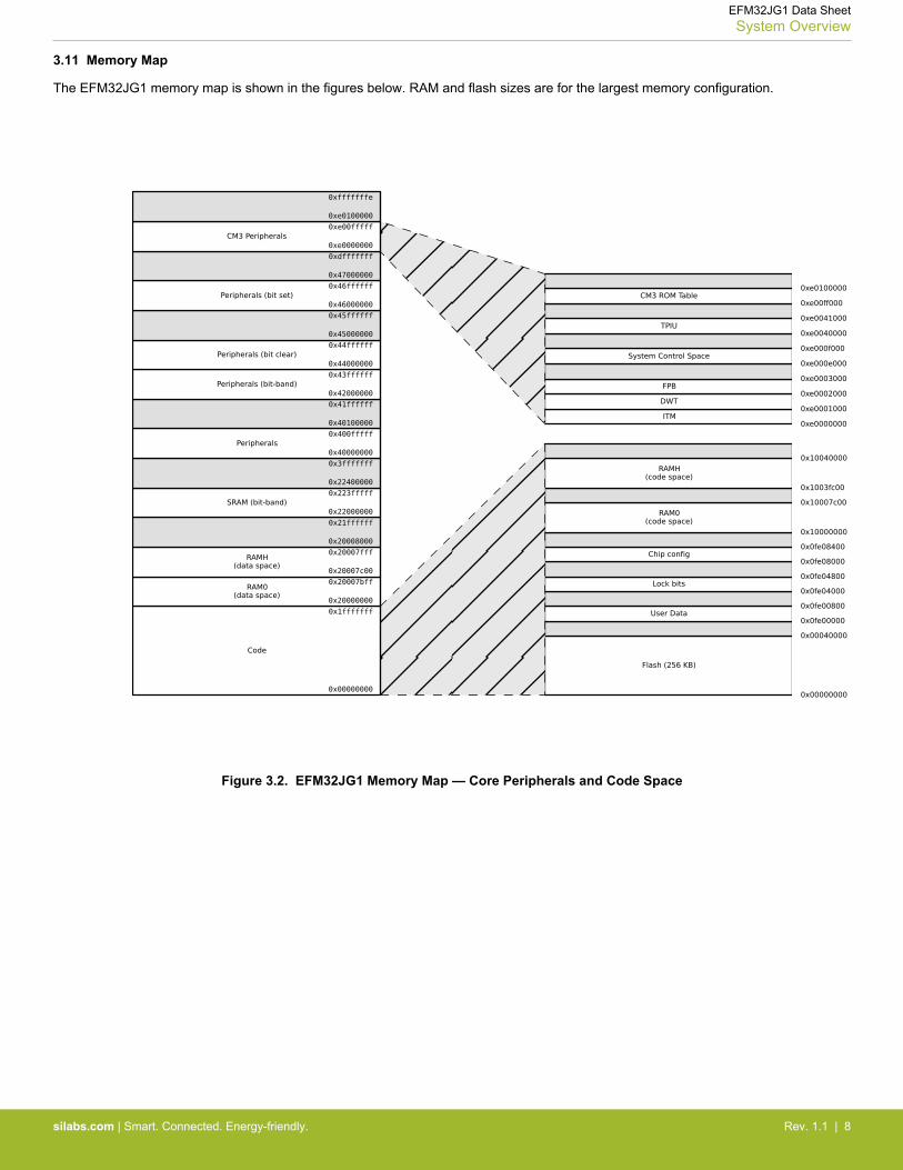
3.11 Memory Map
The EFM32JG1 memory map is shown in the figures below. RAM and flash sizes are for the largest memory configuration.
Figure 3.2. EFM32JG1 Memory Map — Core Peripherals and Code Space
EFM32JG1 Data SheetSystem Overview
silabs.com | Smart. Connected. Energy-friendly. Rev. 1.1 | 8
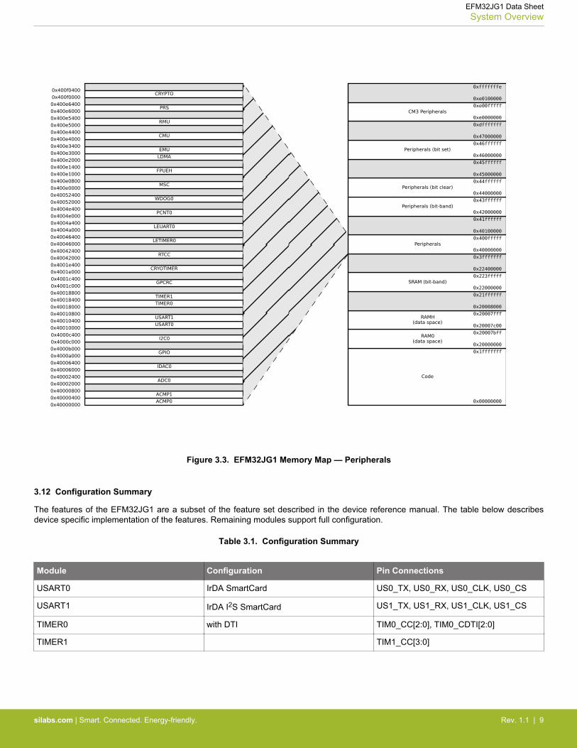
Figure 3.3. EFM32JG1 Memory Map — Peripherals
3.12 Configuration Summary
The features of the EFM32JG1 are a subset of the feature set described in the device reference manual. The table below describesdevice specific implementation of the features. Remaining modules support full configuration.
Table 3.1. Configuration Summary
Module Configuration Pin Connections
USART0 IrDA SmartCard US0_TX, US0_RX, US0_CLK, US0_CS
USART1 IrDA I2S SmartCard US1_TX, US1_RX, US1_CLK, US1_CS
TIMER0 with DTI TIM0_CC[2:0], TIM0_CDTI[2:0]
TIMER1 TIM1_CC[3:0]
EFM32JG1 Data SheetSystem Overview
silabs.com | Smart. Connected. Energy-friendly. Rev. 1.1 | 9

4. Electrical Specifications
4.1 Electrical Characteristics
All electrical parameters in all tables are specified under the following conditions, unless stated otherwise:• Typical values are based on TAMB=25 °C and VDD= 3.3 V, by production test and/or technology characterization.• Minimum and maximum values represent the worst conditions across supply voltage, process variation, and operating temperature,
unless stated otherwise.
Refer to Table 4.2 General Operating Conditions on page 11 for more details about operational supply and temperature limits.
4.1.1 Absolute Maximum Ratings
Stresses above those listed below may cause permanent damage to the device. This is a stress rating only and functional operation ofthe devices at those or any other conditions above those indicated in the operation listings of this specification is not implied. Exposureto maximum rating conditions for extended periods may affect device reliability. For more information on the available quality and relia-bility data, see the Quality and Reliability Monitor Report at http://www.silabs.com/support/quality/pages/default.aspx.
Table 4.1. Absolute Maximum Ratings
Parameter Symbol Test Condition Min Typ Max Unit
Storage temperature range TSTG -50 — 150 °C
External main supply voltage VDDMAX 0 — 3.8 V
External main supply voltageramp rate
VDDRAMPMAX — — 1 V / μs
Voltage on any 5V tolerantGPIO pin1
VDIGPIN -0.3 — Min of 5.25and IOVDD
+2
V
Voltage on non-5V tolerantGPIO pins
-0.3 — IOVDD+0.3 V
Voltage on HFXO pins VHFXOPIN -0.3 — 1.4 V
Total current into VDD powerlines (source)
IVDDMAX — — 200 mA
Total current into VSSground lines (sink)
IVSSMAX — — 200 mA
Current per I/O pin (sink) IIOMAX — — 50 mA
Current per I/O pin (source) — — 50 mA
Current for all I/O pins (sink) IIOALLMAX — — 200 mA
Current for all I/O pins(source)
— — 200 mA
Voltage difference betweenAVDD and VREGVDD
ΔVDD — — 0.3 V
Junction Temperature for -Ggrade devices
TJ -40 — 105 °C
Junction Temperature for -Igrade devices
-40 — 125 °C
Note:1. When a GPIO pin is routed to the analog module through the APORT, the maximum voltage = IOVDD.
EFM32JG1 Data SheetElectrical Specifications
silabs.com | Smart. Connected. Energy-friendly. Rev. 1.1 | 10

4.1.2 Operating Conditions
When assigning supply sources, the following requirements must be observed:• VREGVDD must be the highest voltage in the system• VREGVDD = AVDD• DVDD ≤ AVDD• IOVDD ≤ AVDD
4.1.2.1 General Operating Conditions
Table 4.2. General Operating Conditions
Parameter Symbol Test Condition Min Typ Max Unit
Operating temperature range TOP -G temperature grade, AmbientTemperature
-40 25 85 °C
-I temperature grade, JunctionTemperature
-40 25 125 °C
AVDD Supply voltage1 VAVDD 1.85 3.3 3.8 V
VREGVDD Operating supplyvoltage1 2
VVREGVDD DCDC in regulation 2.4 3.3 3.8 V
DCDC in bypass, 50mA load 1.85 3.3 3.8 V
DCDC not in use. DVDD external-ly shorted to VREGVDD
1.85 3.3 3.8 V
VREGVDD Current IVREGVDD DCDC in bypass, Tamb ≤ 85 °C — — 200 mA
DCDC in bypass, Tamb > 85 °C — — 100 mA
DVDD Operating supply volt-age
VDVDD 1.62 — VVREGVDD V
IOVDD Operating supplyvoltage
VIOVDD 1.62 — VVREGVDD V
Difference between AVDDand VREGVDD, ABS(AVDD-VREGVDD)
dVDD — — 0.1 V
HFCLK frequency fCORE 0 wait-states (MODE = WS0) 3 — — 26 MHz
1 wait-states (MODE = WS1) 3 — — 40 MHz
Note:1. VREGVDD must be tied to AVDD. Both VREGVDD and AVDD minimum voltages must be satisfied for the part to operate.2. The minimum voltage required in bypass mode is calculated using RBYP from the DCDC specification table. Requirements for
other loads can be calculated as VDVDD_min+ILOAD * RBYP_max
3. In MSC_READCTRL register
EFM32JG1 Data SheetElectrical Specifications
silabs.com | Smart. Connected. Energy-friendly. Rev. 1.1 | 11
4.1.3 Thermal Characteristics
Table 4.3. Thermal Characteristics
Parameter Symbol Test Condition Min Typ Max Unit
Thermal Resistance THETAJA QFN32 Package, 2-Layer PCB,Air velocity = 0 m/s
— 79 — °C/W
QFN32 Package, 2-Layer PCB,Air velocity = 1 m/s
— 62.2 — °C/W
QFN32 Package, 2-Layer PCB,Air velocity = 2 m/s
— 54.1 — °C/W
QFN32 Package, 4-Layer PCB,Air velocity = 0 m/s
— 32 — °C/W
QFN32 Package, 4-Layer PCB,Air velocity = 1 m/s
— 28.1 — °C/W
QFN32 Package, 4-Layer PCB,Air velocity = 2 m/s
— 26.9 — °C/W
QFN48 Package, 2-Layer PCB,Air velocity = 0 m/s
— 64.5 — °C/W
QFN48 Package, 2-Layer PCB,Air velocity = 1 m/s
— 51.6 — °C/W
QFN48 Package, 2-Layer PCB,Air velocity = 2 m/s
— 47.7 — °C/W
QFN48 Package, 4-Layer PCB,Air velocity = 0 m/s
— 26.2 — °C/W
QFN48 Package, 4-Layer PCB,Air velocity = 1 m/s
— 23.1 — °C/W
QFN48 Package, 4-Layer PCB,Air velocity = 2 m/s
— 22.1 — °C/W
EFM32JG1 Data SheetElectrical Specifications
silabs.com | Smart. Connected. Energy-friendly. Rev. 1.1 | 12
4.1.4 DC-DC Converter
Test conditions: LDCDC=4.7 µH (Murata LQH3NPN4R7MM0L), CDCDC=1.0 µF (Murata GRM188R71A105KA61D), VDCDC_I=3.3 V,VDCDC_O=1.8 V, IDCDC_LOAD=50 mA, Heavy Drive configuration, FDCDC_LN=7 MHz, unless otherwise indicated.
Table 4.4. DC-DC Converter
Parameter Symbol Test Condition Min Typ Max Unit
Input voltage range VDCDC_I Bypass mode, IDCDC_LOAD = 50mA
1.85 — VVREGVDD_
MAX
V
Low noise (LN) mode, 1.8 V out-put, IDCDC_LOAD = 100 mA, orLow power (LP) mode, 1.8 V out-put, IDCDC_LOAD = 10 mA
2.4 — VVREGVDD_
MAX
V
Low noise (LN) mode, 1.8 V out-put, IDCDC_LOAD = 200 mA
2.6 — VVREGVDD_
MAX
V
Output voltage programma-ble range1
VDCDC_O 1.8 — VVREGVDD V
Regulation DC Accuracy ACCDC Low noise (LN) mode, 1.8 V targetoutput
1.7 — 1.9 V
Regulation Window2 WINREG Low power (LP) mode,LPCMPBIAS3 = 0, 1.8 V targetoutput, IDCDC_LOAD ≤ 75 μA
1.63 — 2.2 V
Low power (LP) mode,LPCMPBIAS3 = 3, 1.8 V targetoutput, IDCDC_LOAD ≤ 10 mA
1.63 — 2.1 V
Steady-state output ripple VR — 3 — mVpp
Output voltage under/over-shoot
VOV CCM Mode (LNFORCECCM3 =1), Load changes between 0 mAand 100 mA
— — 150 mV
DCM Mode (LNFORCECCM3 =0), Load changes between 0 mAand 10 mA
— — 150 mV
Overshoot during LP to LNCCM/DCM mode transitions com-pared to DC level in LN mode
— 200 — mV
Undershoot during BYP/LP to LNCCM (LNFORCECCM3 = 1) modetransitions compared to DC levelin LN mode
— 50 — mV
Undershoot during BYP/LP to LNDCM (LNFORCECCM3 = 0) modetransitions compared to DC levelin LN mode
— 125 — mV
DC line regulation VREG Input changes betweenVVREGVDD_MAX and 2.4 V
— 0.1 — %
DC load regulation IREG Load changes between 0 mA and100 mA in CCM mode
— 0.1 — %
EFM32JG1 Data SheetElectrical Specifications
silabs.com | Smart. Connected. Energy-friendly. Rev. 1.1 | 13

Parameter Symbol Test Condition Min Typ Max Unit
Max load current ILOAD_MAX Low noise (LN) mode, HeavyDrive4, Tamb ≤ 85 °C
— — 200 mA
Low noise (LN) mode, HeavyDrive4, Tamb > 85 °C
— — 100 mA
Low noise (LN) mode, MediumDrive4
— — 100 mA
Low noise (LN) mode, LightDrive4
— — 50 mA
Low power (LP) mode,LPCMPBIAS3 = 0
— — 75 μA
Low power (LP) mode,LPCMPBIAS3 = 3
— — 10 mA
DCDC nominal output ca-pacitor
CDCDC 25% tolerance 1 1 1 μF
DCDC nominal output induc-tor
LDCDC 20% tolerance 4.7 4.7 4.7 μH
Resistance in Bypass mode RBYP — 1.2 2.5 Ω
Note:1. Due to internal dropout, the DC-DC output will never be able to reach its input voltage, VVREGVDD
2. LP mode controller is a hysteretic controller that maintains the output voltage within the specified limits3. In EMU_DCDCMISCCTRL register4. Drive levels are defined by configuration of the PFETCNT and NFETCNT registers. Light Drive: PFETCNT=NFETCNT=3; Medi-
um Drive: PFETCNT=NFETCNT=7; Heavy Drive: PFETCNT=NFETCNT=15.
EFM32JG1 Data SheetElectrical Specifications
silabs.com | Smart. Connected. Energy-friendly. Rev. 1.1 | 14
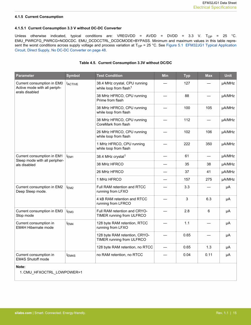
4.1.5 Current Consumption
4.1.5.1 Current Consumption 3.3 V without DC-DC Converter
Unless otherwise indicated, typical conditions are: VREGVDD = AVDD = DVDD = 3.3 V. TOP = 25 °C.EMU_PWRCFG_PWRCG=NODCDC. EMU_DCDCCTRL_DCDCMODE=BYPASS. Minimum and maximum values in this table repre-sent the worst conditions across supply voltage and process variation at TOP = 25 °C. See Figure 5.1 EFM32JG1 Typical ApplicationCircuit, Direct Supply, No DC-DC Converter on page 48.
Table 4.5. Current Consumption 3.3V without DC/DC
Parameter Symbol Test Condition Min Typ Max Unit
Current consumption in EM0Active mode with all periph-erals disabled
IACTIVE 38.4 MHz crystal, CPU runningwhile loop from flash1
— 127 — μA/MHz
38 MHz HFRCO, CPU runningPrime from flash
— 88 — μA/MHz
38 MHz HFRCO, CPU runningwhile loop from flash
— 100 105 μA/MHz
38 MHz HFRCO, CPU runningCoreMark from flash
— 112 — μA/MHz
26 MHz HFRCO, CPU runningwhile loop from flash
— 102 106 μA/MHz
1 MHz HFRCO, CPU runningwhile loop from flash
— 222 350 μA/MHz
Current consumption in EM1Sleep mode with all peripher-als disabled
IEM1 38.4 MHz crystal1 — 61 — μA/MHz
38 MHz HFRCO — 35 38 μA/MHz
26 MHz HFRCO — 37 41 μA/MHz
1 MHz HFRCO — 157 275 μA/MHz
Current consumption in EM2Deep Sleep mode.
IEM2 Full RAM retention and RTCCrunning from LFXO
— 3.3 — μA
4 kB RAM retention and RTCCrunning from LFRCO
— 3 6.3 μA
Current consumption in EM3Stop mode
IEM3 Full RAM retention and CRYO-TIMER running from ULFRCO
— 2.8 6 μA
Current consumption inEM4H Hibernate mode
IEM4 128 byte RAM retention, RTCCrunning from LFXO
— 1.1 — μA
128 byte RAM retention, CRYO-TIMER running from ULFRCO
— 0.65 — μA
128 byte RAM retention, no RTCC — 0.65 1.3 μA
Current consumption inEM4S Shutoff mode
IEM4S no RAM retention, no RTCC — 0.04 0.11 μA
Note:1. CMU_HFXOCTRL_LOWPOWER=1
EFM32JG1 Data SheetElectrical Specifications
silabs.com | Smart. Connected. Energy-friendly. Rev. 1.1 | 15

4.1.5.2 Current Consumption 3.3 V using DC-DC Converter
Unless otherwise indicated, typical conditions are: VREGVDD = AVDD = IOVDD = 3.3 V, DVDD = 1.8 V DC-DC output. TOP = 25 °C.Minimum and maximum values in this table represent the worst conditions across supply voltage and process variation at TOP = 25 °C.See Figure 5.2 EFM32JG1 Typical Application Circuit Using the DC-DC Converter on page 48.
Table 4.6. Current Consumption 3.3V with DC-DC
Parameter Symbol Test Condition Min Typ Max Unit
Current consumption in EM0Active mode with all periph-erals disabled, DCDC in LowNoise DCM mode1.
IACTIVE 38.4 MHz crystal, CPU runningwhile loop from flash2
— 86 — μA/MHz
38 MHz HFRCO, CPU runningPrime from flash
— 63 — μA/MHz
38 MHz HFRCO, CPU runningwhile loop from flash
— 71 — μA/MHz
38 MHz HFRCO, CPU runningCoreMark from flash
— 78 — μA/MHz
26 MHz HFRCO, CPU runningwhile loop from flash
— 76 — μA/MHz
Current consumption in EM0Active mode with all periph-erals disabled, DCDC in LowNoise CCM mode3.
38.4 MHz crystal, CPU runningwhile loop from flash2
— 96 — μA/MHz
38 MHz HFRCO, CPU runningPrime from flash
— 75 — μA/MHz
38 MHz HFRCO, CPU runningwhile loop from flash
— 81 — μA/MHz
38 MHz HFRCO, CPU runningCoreMark from flash
— 88 — μA/MHz
26 MHz HFRCO, CPU runningwhile loop from flash
— 94 — μA/MHz
Current consumption in EM1Sleep mode with all peripher-als disabled, DCDC in LowNoise DCM mode1.
IEM1 38.4 MHz crystal2 — 47 — μA/MHz
38 MHz HFRCO — 32 — μA/MHz
26 MHz HFRCO — 38 — μA/MHz
Current consumption in EM1Sleep mode with all peripher-als disabled, DCDC in LowNoise CCM mode3.
38.4 MHz crystal2 — 59 — μA/MHz
38 MHz HFRCO — 45 — μA/MHz
26 MHz HFRCO — 58 — μA/MHz
Current consumption in EM2Deep Sleep mode. DCDC inLow Power mode4.
IEM2 Full RAM retention and RTCCrunning from LFXO
— 2.5 — μA
4 kB RAM retention and RTCCrunning from LFRCO
— 2.2 — μA
Current consumption in EM3Stop mode
IEM3 Full RAM retention and CRYO-TIMER running from ULFRCO
— 2.1 — μA
Current consumption inEM4H Hibernate mode
IEM4 128 byte RAM retention, RTCCrunning from LFXO
— 0.86 — μA
128 byte RAM retention, CRYO-TIMER running from ULFRCO
— 0.58 — μA
128 byte RAM retention, no RTCC — 0.58 — μA
EFM32JG1 Data SheetElectrical Specifications
silabs.com | Smart. Connected. Energy-friendly. Rev. 1.1 | 16
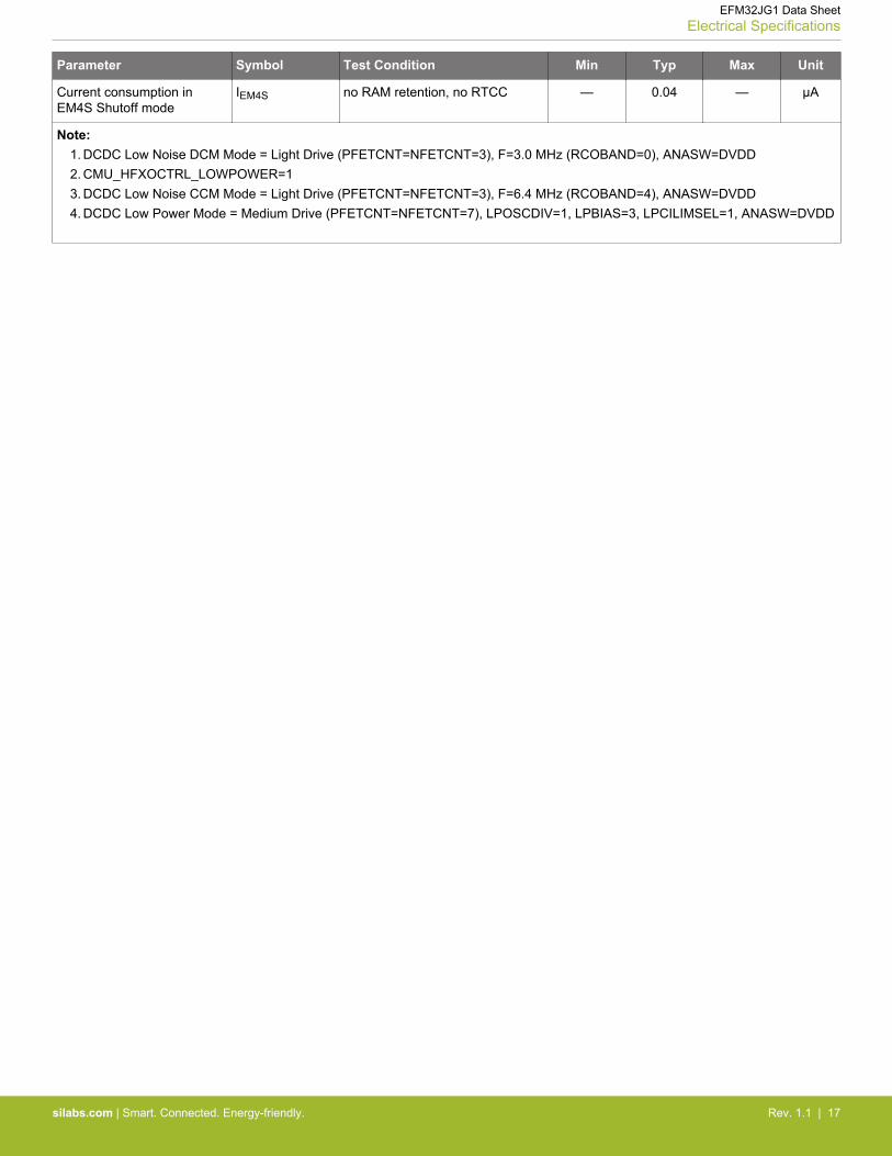
Parameter Symbol Test Condition Min Typ Max Unit
Current consumption inEM4S Shutoff mode
IEM4S no RAM retention, no RTCC — 0.04 — μA
Note:1. DCDC Low Noise DCM Mode = Light Drive (PFETCNT=NFETCNT=3), F=3.0 MHz (RCOBAND=0), ANASW=DVDD2. CMU_HFXOCTRL_LOWPOWER=13. DCDC Low Noise CCM Mode = Light Drive (PFETCNT=NFETCNT=3), F=6.4 MHz (RCOBAND=4), ANASW=DVDD4. DCDC Low Power Mode = Medium Drive (PFETCNT=NFETCNT=7), LPOSCDIV=1, LPBIAS=3, LPCILIMSEL=1, ANASW=DVDD
EFM32JG1 Data SheetElectrical Specifications
silabs.com | Smart. Connected. Energy-friendly. Rev. 1.1 | 17
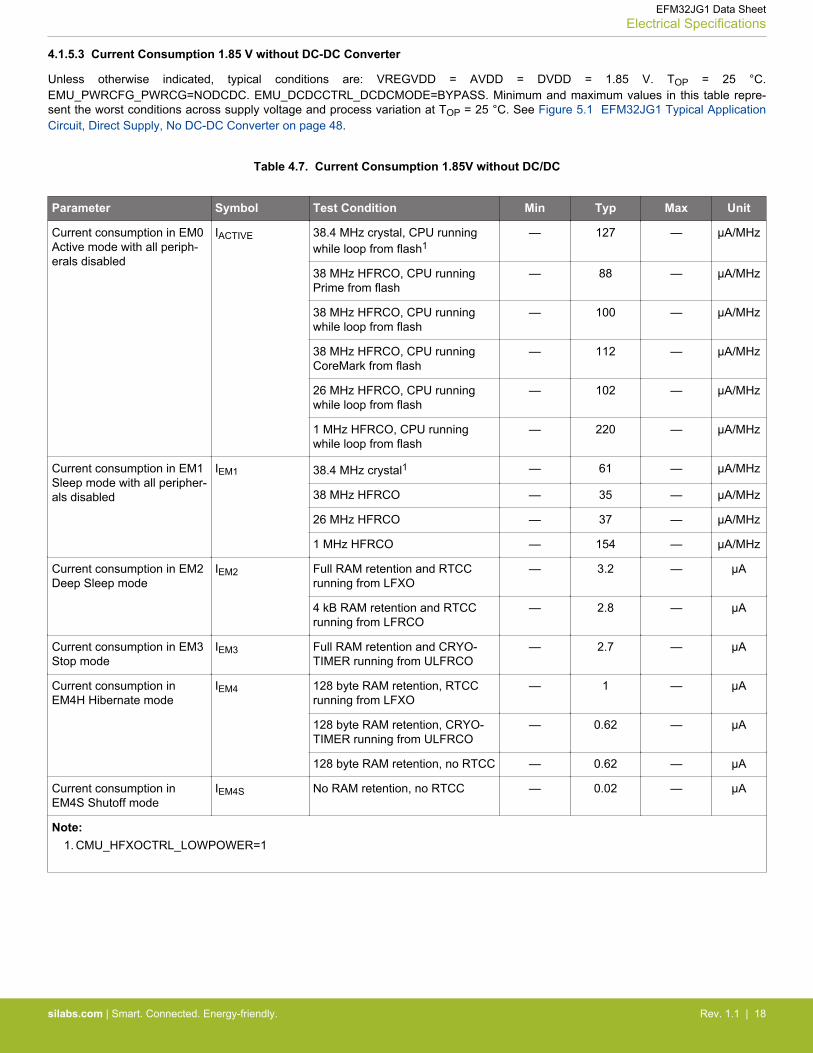
4.1.5.3 Current Consumption 1.85 V without DC-DC Converter
Unless otherwise indicated, typical conditions are: VREGVDD = AVDD = DVDD = 1.85 V. TOP = 25 °C.EMU_PWRCFG_PWRCG=NODCDC. EMU_DCDCCTRL_DCDCMODE=BYPASS. Minimum and maximum values in this table repre-sent the worst conditions across supply voltage and process variation at TOP = 25 °C. See Figure 5.1 EFM32JG1 Typical ApplicationCircuit, Direct Supply, No DC-DC Converter on page 48.
Table 4.7. Current Consumption 1.85V without DC/DC
Parameter Symbol Test Condition Min Typ Max Unit
Current consumption in EM0Active mode with all periph-erals disabled
IACTIVE 38.4 MHz crystal, CPU runningwhile loop from flash1
— 127 — μA/MHz
38 MHz HFRCO, CPU runningPrime from flash
— 88 — μA/MHz
38 MHz HFRCO, CPU runningwhile loop from flash
— 100 — μA/MHz
38 MHz HFRCO, CPU runningCoreMark from flash
— 112 — μA/MHz
26 MHz HFRCO, CPU runningwhile loop from flash
— 102 — μA/MHz
1 MHz HFRCO, CPU runningwhile loop from flash
— 220 — μA/MHz
Current consumption in EM1Sleep mode with all peripher-als disabled
IEM1 38.4 MHz crystal1 — 61 — μA/MHz
38 MHz HFRCO — 35 — μA/MHz
26 MHz HFRCO — 37 — μA/MHz
1 MHz HFRCO — 154 — μA/MHz
Current consumption in EM2Deep Sleep mode
IEM2 Full RAM retention and RTCCrunning from LFXO
— 3.2 — μA
4 kB RAM retention and RTCCrunning from LFRCO
— 2.8 — μA
Current consumption in EM3Stop mode
IEM3 Full RAM retention and CRYO-TIMER running from ULFRCO
— 2.7 — μA
Current consumption inEM4H Hibernate mode
IEM4 128 byte RAM retention, RTCCrunning from LFXO
— 1 — μA
128 byte RAM retention, CRYO-TIMER running from ULFRCO
— 0.62 — μA
128 byte RAM retention, no RTCC — 0.62 — μA
Current consumption inEM4S Shutoff mode
IEM4S No RAM retention, no RTCC — 0.02 — μA
Note:1. CMU_HFXOCTRL_LOWPOWER=1
EFM32JG1 Data SheetElectrical Specifications
silabs.com | Smart. Connected. Energy-friendly. Rev. 1.1 | 18
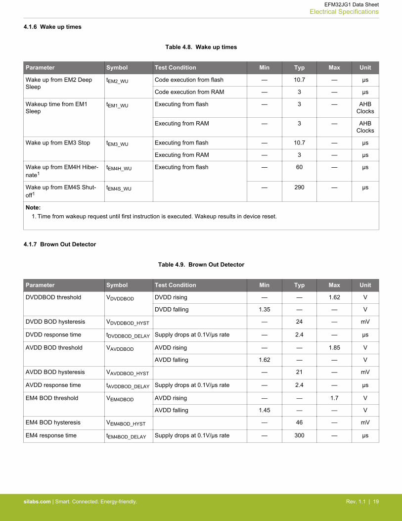
4.1.6 Wake up times
Table 4.8. Wake up times
Parameter Symbol Test Condition Min Typ Max Unit
Wake up from EM2 DeepSleep
tEM2_WU Code execution from flash — 10.7 — μs
Code execution from RAM — 3 — μs
Wakeup time from EM1Sleep
tEM1_WU Executing from flash — 3 — AHBClocks
Executing from RAM — 3 — AHBClocks
Wake up from EM3 Stop tEM3_WU Executing from flash — 10.7 — μs
Executing from RAM — 3 — μs
Wake up from EM4H Hiber-nate1
tEM4H_WU Executing from flash — 60 — μs
Wake up from EM4S Shut-off1
tEM4S_WU — 290 — μs
Note:1. Time from wakeup request until first instruction is executed. Wakeup results in device reset.
4.1.7 Brown Out Detector
Table 4.9. Brown Out Detector
Parameter Symbol Test Condition Min Typ Max Unit
DVDDBOD threshold VDVDDBOD DVDD rising — — 1.62 V
DVDD falling 1.35 — — V
DVDD BOD hysteresis VDVDDBOD_HYST — 24 — mV
DVDD response time tDVDDBOD_DELAY Supply drops at 0.1V/μs rate — 2.4 — μs
AVDD BOD threshold VAVDDBOD AVDD rising — — 1.85 V
AVDD falling 1.62 — — V
AVDD BOD hysteresis VAVDDBOD_HYST — 21 — mV
AVDD response time tAVDDBOD_DELAY Supply drops at 0.1V/μs rate — 2.4 — μs
EM4 BOD threshold VEM4DBOD AVDD rising — — 1.7 V
AVDD falling 1.45 — — V
EM4 BOD hysteresis VEM4BOD_HYST — 46 — mV
EM4 response time tEM4BOD_DELAY Supply drops at 0.1V/μs rate — 300 — μs
EFM32JG1 Data SheetElectrical Specifications
silabs.com | Smart. Connected. Energy-friendly. Rev. 1.1 | 19
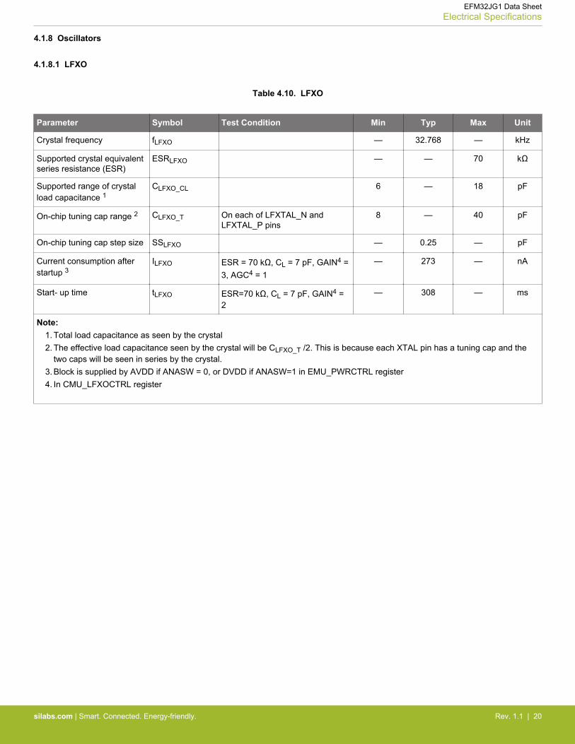
4.1.8 Oscillators
4.1.8.1 LFXO
Table 4.10. LFXO
Parameter Symbol Test Condition Min Typ Max Unit
Crystal frequency fLFXO — 32.768 — kHz
Supported crystal equivalentseries resistance (ESR)
ESRLFXO — — 70 kΩ
Supported range of crystalload capacitance 1
CLFXO_CL 6 — 18 pF
On-chip tuning cap range 2 CLFXO_T On each of LFXTAL_N andLFXTAL_P pins
8 — 40 pF
On-chip tuning cap step size SSLFXO — 0.25 — pF
Current consumption afterstartup 3
ILFXO ESR = 70 kΩ, CL = 7 pF, GAIN4 =3, AGC4 = 1
— 273 — nA
Start- up time tLFXO ESR=70 kΩ, CL = 7 pF, GAIN4 =2
— 308 — ms
Note:1. Total load capacitance as seen by the crystal2. The effective load capacitance seen by the crystal will be CLFXO_T /2. This is because each XTAL pin has a tuning cap and the
two caps will be seen in series by the crystal.3. Block is supplied by AVDD if ANASW = 0, or DVDD if ANASW=1 in EMU_PWRCTRL register4. In CMU_LFXOCTRL register
EFM32JG1 Data SheetElectrical Specifications
silabs.com | Smart. Connected. Energy-friendly. Rev. 1.1 | 20
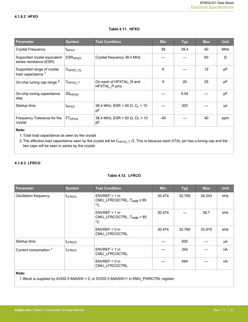
4.1.8.2 HFXO
Table 4.11. HFXO
Parameter Symbol Test Condition Min Typ Max Unit
Crystal Frequency fHFXO 38 38.4 40 MHz
Supported crystal equivalentseries resistance (ESR)
ESRHFXO Crystal frequency 38.4 MHz — — 60 Ω
Supported range of crystalload capacitance 1
CHFXO_CL 6 — 12 pF
On-chip tuning cap range 2 CHFXO_T On each of HFXTAL_N andHFXTAL_P pins
9 20 25 pF
On-chip tuning capacitancestep
SSHFXO — 0.04 — pF
Startup time tHFXO 38.4 MHz, ESR = 50 Ω, CL = 10pF
— 300 — μs
Frequency Tolerance for thecrystal
FTHFXO 38.4 MHz, ESR = 50 Ω, CL = 10pF
-40 — 40 ppm
Note:1. Total load capacitance as seen by the crystal2. The effective load capacitance seen by the crystal will be CHFXO_T /2. This is because each XTAL pin has a tuning cap and the
two caps will be seen in series by the crystal.
4.1.8.3 LFRCO
Table 4.12. LFRCO
Parameter Symbol Test Condition Min Typ Max Unit
Oscillation frequency fLFRCO ENVREF = 1 inCMU_LFRCOCTRL, TAMB ≤ 85°C
30.474 32.768 34.243 kHz
ENVREF = 1 inCMU_LFRCOCTRL, TAMB > 85°C
30.474 — 39.7 kHz
ENVREF = 0 inCMU_LFRCOCTRL
30.474 32.768 33.915 kHz
Startup time tLFRCO — 500 — μs
Current consumption 1 ILFRCO ENVREF = 1 inCMU_LFRCOCTRL
— 342 — nA
ENVREF = 0 inCMU_LFRCOCTRL
— 494 — nA
Note:1. Block is supplied by AVDD if ANASW = 0, or DVDD if ANASW=1 in EMU_PWRCTRL register
EFM32JG1 Data SheetElectrical Specifications
silabs.com | Smart. Connected. Energy-friendly. Rev. 1.1 | 21
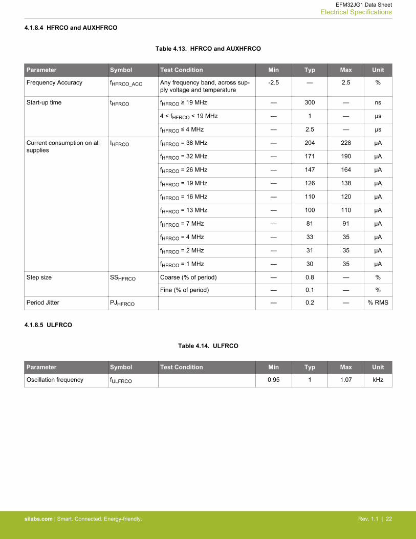
4.1.8.4 HFRCO and AUXHFRCO
Table 4.13. HFRCO and AUXHFRCO
Parameter Symbol Test Condition Min Typ Max Unit
Frequency Accuracy fHFRCO_ACC Any frequency band, across sup-ply voltage and temperature
-2.5 — 2.5 %
Start-up time tHFRCO fHFRCO ≥ 19 MHz — 300 — ns
4 < fHFRCO < 19 MHz — 1 — μs
fHFRCO ≤ 4 MHz — 2.5 — μs
Current consumption on allsupplies
IHFRCO fHFRCO = 38 MHz — 204 228 μA
fHFRCO = 32 MHz — 171 190 μA
fHFRCO = 26 MHz — 147 164 μA
fHFRCO = 19 MHz — 126 138 μA
fHFRCO = 16 MHz — 110 120 μA
fHFRCO = 13 MHz — 100 110 μA
fHFRCO = 7 MHz — 81 91 μA
fHFRCO = 4 MHz — 33 35 μA
fHFRCO = 2 MHz — 31 35 μA
fHFRCO = 1 MHz — 30 35 μA
Step size SSHFRCO Coarse (% of period) — 0.8 — %
Fine (% of period) — 0.1 — %
Period Jitter PJHFRCO — 0.2 — % RMS
4.1.8.5 ULFRCO
Table 4.14. ULFRCO
Parameter Symbol Test Condition Min Typ Max Unit
Oscillation frequency fULFRCO 0.95 1 1.07 kHz
EFM32JG1 Data SheetElectrical Specifications
silabs.com | Smart. Connected. Energy-friendly. Rev. 1.1 | 22

4.1.9 Flash Memory Characteristics
Table 4.15. Flash Memory Characteristics1
Parameter Symbol Test Condition Min Typ Max Unit
Flash erase cycles beforefailure
ECFLASH 10000 — — cycles
Flash data retention RETFLASH TAMB ≤ 85 °C 10 — — years
TAMB ≤ 125 °C 10 — — years
Word (32-bit) programmingtime
tW_PROG 20 26 40 μs
Page erase time tPERASE 20 27 40 ms
Mass erase time tMERASE 20 27 40 ms
Device erase time2 tDERASE TAMB ≤ 85 °C — 60 74 ms
TAMB ≤ 125 °C — 60 78 ms
Page erase current3 IERASE — — 3 mA
Mass or Device erase cur-rent3
— — 5 mA
Write current3 IWRITE — — 3 mA
Note:1. Flash data retention information is published in the Quarterly Quality and Reliability Report.2. Device erase is issued over the AAP interface and erases all flash, SRAM, the Lock Bit (LB) page, and the User data page Lock
Word (ULW)3. Measured at 25°C
EFM32JG1 Data SheetElectrical Specifications
silabs.com | Smart. Connected. Energy-friendly. Rev. 1.1 | 23

4.1.10 GPIO
Table 4.16. GPIO
Parameter Symbol Test Condition Min Typ Max Unit
Input low voltage VIOIL — — IOVDD*0.3 V
Input high voltage VIOIH IOVDD*0.7 — — V
Output high voltage relativeto IOVDD
VIOOH Sourcing 3 mA, IOVDD ≥ 3 V,
DRIVESTRENGTH1 = WEAK
IOVDD*0.8 — — V
Sourcing 1.2 mA, IOVDD ≥ 1.62V,
DRIVESTRENGTH1 = WEAK
IOVDD*0.6 — — V
Sourcing 20 mA, IOVDD ≥ 3 V,
DRIVESTRENGTH1 = STRONG
IOVDD*0.8 — — V
Sourcing 8 mA, IOVDD ≥ 1.62 V,
DRIVESTRENGTH1 = STRONG
IOVDD*0.6 — — V
Output low voltage relative toIOVDD
VIOOL Sinking 3 mA, IOVDD ≥ 3 V,
DRIVESTRENGTH1 = WEAK
— — IOVDD*0.2 V
Sinking 1.2 mA, IOVDD ≥ 1.62 V,
DRIVESTRENGTH1 = WEAK
— — IOVDD*0.4 V
Sinking 20 mA, IOVDD ≥ 3 V,
DRIVESTRENGTH1 = STRONG
— — IOVDD*0.2 V
Sinking 8 mA, IOVDD ≥ 1.62 V,
DRIVESTRENGTH1 = STRONG
— — IOVDD*0.4 V
Input leakage current IIOLEAK All GPIO except LFXO pins, GPIO≤ IOVDD, Tamb ≤ 85 °C
— 0.1 30 nA
LFXO Pins, GPIO ≤ IOVDD, Tamb≤ 85 °C
— 0.1 50 nA
All GPIO except LFXO pins, GPIO≤ IOVDD, TAMB > 85 °C
— — 110 nA
LFXO Pins, GPIO ≤ IOVDD, TAMB> 85 °C
— — 250 nA
Input leakage current on5VTOL pads above IOVDD
I5VTOLLEAK IOVDD < GPIO ≤ IOVDD + 2 V — 3.3 15 μA
I/O pin pull-up resistor RPU 30 43 65 kΩ
I/O pin pull-down resistor RPD 30 43 65 kΩ
Pulse width of pulses re-moved by the glitch suppres-sion filter
tIOGLITCH 20 25 35 ns
EFM32JG1 Data SheetElectrical Specifications
silabs.com | Smart. Connected. Energy-friendly. Rev. 1.1 | 24

Parameter Symbol Test Condition Min Typ Max Unit
Output fall time, From 70%to 30% of VIO
tIOOF CL = 50 pF,
DRIVESTRENGTH1 = STRONG,
SLEWRATE1 = 0x6
— 1.8 — ns
CL = 50 pF,
DRIVESTRENGTH1 = WEAK,
SLEWRATE1 = 0x6
— 4.5 — ns
Output rise time, From 30%to 70% of VIO
tIOOR CL = 50 pF,
DRIVESTRENGTH1 = STRONG,
SLEWRATE = 0x61
— 2.2 — ns
CL = 50 pF,
DRIVESTRENGTH1 = WEAK,
SLEWRATE1 = 0x6
— 7.4 — ns
Note:1. In GPIO_Pn_CTRL register
4.1.11 VMON
Table 4.17. VMON
Parameter Symbol Test Condition Min Typ Max Unit
VMON Supply Current IVMON In EM0 or EM1, 1 supply moni-tored
— 5.8 8.26 μA
In EM0 or EM1, 4 supplies moni-tored
— 11.8 16.8 μA
In EM2, EM3 or EM4, 1 supplymonitored
— 62 — nA
In EM2, EM3 or EM4, 4 suppliesmonitored
— 99 — nA
VMON Loading of MonitoredSupply
ISENSE In EM0 or EM1 — 2 — μA
In EM2, EM3 or EM4 — 2 — nA
Threshold range VVMON_RANGE 1.62 — 3.4 V
Threshold step size NVMON_STESP Coarse — 200 — mV
Fine — 20 — mV
Response time tVMON_RES Supply drops at 1V/μs rate — 460 — ns
Hysteresis VVMON_HYST — 26 — mV
EFM32JG1 Data SheetElectrical Specifications
silabs.com | Smart. Connected. Energy-friendly. Rev. 1.1 | 25

4.1.12 ADC
Table 4.18. ADC
Parameter Symbol Test Condition Min Typ Max Unit
Resolution VRESOLUTION 6 — 12 Bits
Input voltage range VADCIN Single ended 0 — 2*VREF V
Differential -VREF — VREF V
Input range of external refer-ence voltage, single endedand differential
VADCREFIN_P 1 — VAVDD V
Power supply rejection1 PSRRADC At DC — 80 — dB
Analog input common moderejection ratio
CMRRADC At DC — 80 — dB
Current from all supplies, us-ing internal reference buffer.Continous operation. WAR-MUPMODE2 = KEEPADC-WARM
IADC_CONTI-
NOUS_LP
1 Msps / 16 MHz ADCCLK,
BIASPROG = 0, GPBIASACC = 13
— 301 350 μA
250 ksps / 4 MHz ADCCLK, BIA-SPROG = 6, GPBIASACC = 1 3
— 149 — μA
62.5 ksps / 1 MHz ADCCLK,
BIASPROG = 15, GPBIASACC =1 3
— 91 — μA
Current from all supplies, us-ing internal reference buffer.Duty-cycled operation. WAR-MUPMODE2 = NORMAL
IADC_NORMAL_LP 35 ksps / 16 MHz ADCCLK,
BIASPROG = 0, GPBIASACC = 13
— 51 — μA
5 ksps / 16 MHz ADCCLK
BIASPROG = 0, GPBIASACC = 13
— 9 — μA
Current from all supplies, us-ing internal reference buffer.Duty-cycled operation.AWARMUPMODE2 = KEEP-INSTANDBY or KEEPIN-SLOWACC
IADC_STAND-
BY_LP
125 ksps / 16 MHz ADCCLK,
BIASPROG = 0, GPBIASACC = 13
— 117 — μA
35 ksps / 16 MHz ADCCLK,
BIASPROG = 0, GPBIASACC = 13
— 79 — μA
Current from all supplies, us-ing internal reference buffer.Continous operation. WAR-MUPMODE2 = KEEPADC-WARM
IADC_CONTI-
NOUS_HP
1 Msps / 16 MHz ADCCLK,
BIASPROG = 0, GPBIASACC = 03
— 345 — μA
250 ksps / 4 MHz ADCCLK, BIA-SPROG = 6, GPBIASACC = 0 3
— 191 — μA
62.5 ksps / 1 MHz ADCCLK,
BIASPROG = 15, GPBIASACC =0 3
— 132 — μA
EFM32JG1 Data SheetElectrical Specifications
silabs.com | Smart. Connected. Energy-friendly. Rev. 1.1 | 26
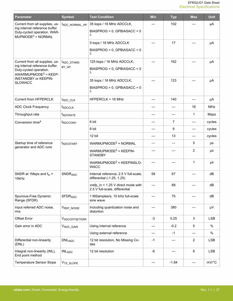
Parameter Symbol Test Condition Min Typ Max Unit
Current from all supplies, us-ing internal reference buffer.Duty-cycled operation. WAR-MUPMODE2 = NORMAL
IADC_NORMAL_HP 35 ksps / 16 MHz ADCCLK,
BIASPROG = 0, GPBIASACC = 03
— 102 — μA
5 ksps / 16 MHz ADCCLK
BIASPROG = 0, GPBIASACC = 03
— 17 — μA
Current from all supplies, us-ing internal reference buffer.Duty-cycled operation.AWARMUPMODE2 = KEEP-INSTANDBY or KEEPIN-SLOWACC
IADC_STAND-
BY_HP
125 ksps / 16 MHz ADCCLK,
BIASPROG = 0, GPBIASACC = 03
— 162 — μA
35 ksps / 16 MHz ADCCLK,
BIASPROG = 0, GPBIASACC = 03
— 123 — μA
Current from HFPERCLK IADC_CLK HFPERCLK = 16 MHz — 140 — μA
ADC Clock Frequency fADCCLK — — 16 MHz
Throughput rate fADCRATE — — 1 Msps
Conversion time4 tADCCONV 6 bit — 7 — cycles
8 bit — 9 — cycles
12 bit — 13 — cycles
Startup time of referencegenerator and ADC core
tADCSTART WARMUPMODE2 = NORMAL — — 5 μs
WARMUPMODE2 = KEEPIN-STANDBY
— — 2 μs
WARMUPMODE2 = KEEPINSLO-WACC
— — 1 μs
SNDR at 1Msps and fin =10kHz
SNDRADC Internal reference, 2.5 V full-scale,differential (-1.25, 1.25)
58 67 — dB
vrefp_in = 1.25 V direct mode with2.5 V full-scale, differential
— 68 — dB
Spurious-Free DynamicRange (SFDR)
SFDRADC 1 MSamples/s, 10 kHz full-scalesine wave
— 75 — dB
Input referred ADC noise,rms
VREF_NOISE Including quantization noise anddistortion
— 380 — μV
Offset Error VADCOFFSETERR -3 0.25 3 LSB
Gain error in ADC VADC_GAIN Using internal reference — -0.2 5 %
Using external reference — -1 — %
Differential non-linearity(DNL)
DNLADC 12 bit resolution, No Missing Co-des
-1 — 2 LSB
Integral non-linearity (INL),End point method
INLADC 12 bit resolution -6 — 6 LSB
Temperature Sensor Slope VTS_SLOPE — -1.84 — mV/°C
EFM32JG1 Data SheetElectrical Specifications
silabs.com | Smart. Connected. Energy-friendly. Rev. 1.1 | 27

Parameter Symbol Test Condition Min Typ Max Unit
Note:1. PSRR is referenced to AVDD when ANASW=0 and to DVDD when ANASW=1 in EMU_PWRCTRL2. In ADCn_CNTL register3. In ADCn_BIASPROG register4. Derived from ADCCLK
EFM32JG1 Data SheetElectrical Specifications
silabs.com | Smart. Connected. Energy-friendly. Rev. 1.1 | 28

4.1.13 IDAC
Table 4.19. IDAC
Parameter Symbol Test Condition Min Typ Max Unit
Number of Ranges NIDAC_RANGES — 4 — -
Output Current IIDAC_OUT RANGSEL1 = RANGE0 0.05 — 1.6 μA
RANGSEL1 = RANGE1 1.6 — 4.7 μA
RANGSEL1 = RANGE2 0.5 — 16 μA
RANGSEL1 = RANGE3 2 — 64 μA
Linear steps within eachrange
NIDAC_STEPS — 32 —
Step size SSIDAC RANGSEL1 = RANGE0 — 50 — nA
RANGSEL1 = RANGE1 — 100 — nA
RANGSEL1 = RANGE2 — 500 — nA
RANGSEL1 = RANGE3 — 2 — μA
Total Accuracy, STEPSEL1 =0x10
ACCIDAC EM0 or EM1, AVDD=3.3 V, T = 25°C
-2 — 2 %
EM0 or EM1 -18 — 22 %
EM2 or EM3, Source mode,RANGSEL1 = RANGE0,AVDD=3.3 V, T = 25 °C
— -2 — %
EM2 or EM3, Source mode,RANGSEL1 = RANGE1,AVDD=3.3 V, T = 25 °C
— -1.7 — %
EM2 or EM3, Source mode,RANGSEL1 = RANGE2,AVDD=3.3 V, T = 25 °C
— -0.8 — %
EM2 or EM3, Source mode,RANGSEL1 = RANGE3,AVDD=3.3 V, T = 25 °C
— -0.5 — %
EM2 or EM3, Sink mode, RANG-SEL1 = RANGE0, AVDD=3.3 V, T= 25 °C
— -0.7 — %
EM2 or EM3, Sink mode, RANG-SEL1 = RANGE1, AVDD=3.3 V, T= 25 °C
— -0.6 — %
EM2 or EM3, Sink mode, RANG-SEL1 = RANGE2, AVDD=3.3 V, T= 25 °C
— -0.5 — %
EM2 or EM3, Sink mode, RANG-SEL1 = RANGE3, AVDD=3.3 V, T= 25 °C
— -0.5 — %
Start up time tIDAC_SU Output within 1% of steady statevalue
— 5 — μs
EFM32JG1 Data SheetElectrical Specifications
silabs.com | Smart. Connected. Energy-friendly. Rev. 1.1 | 29
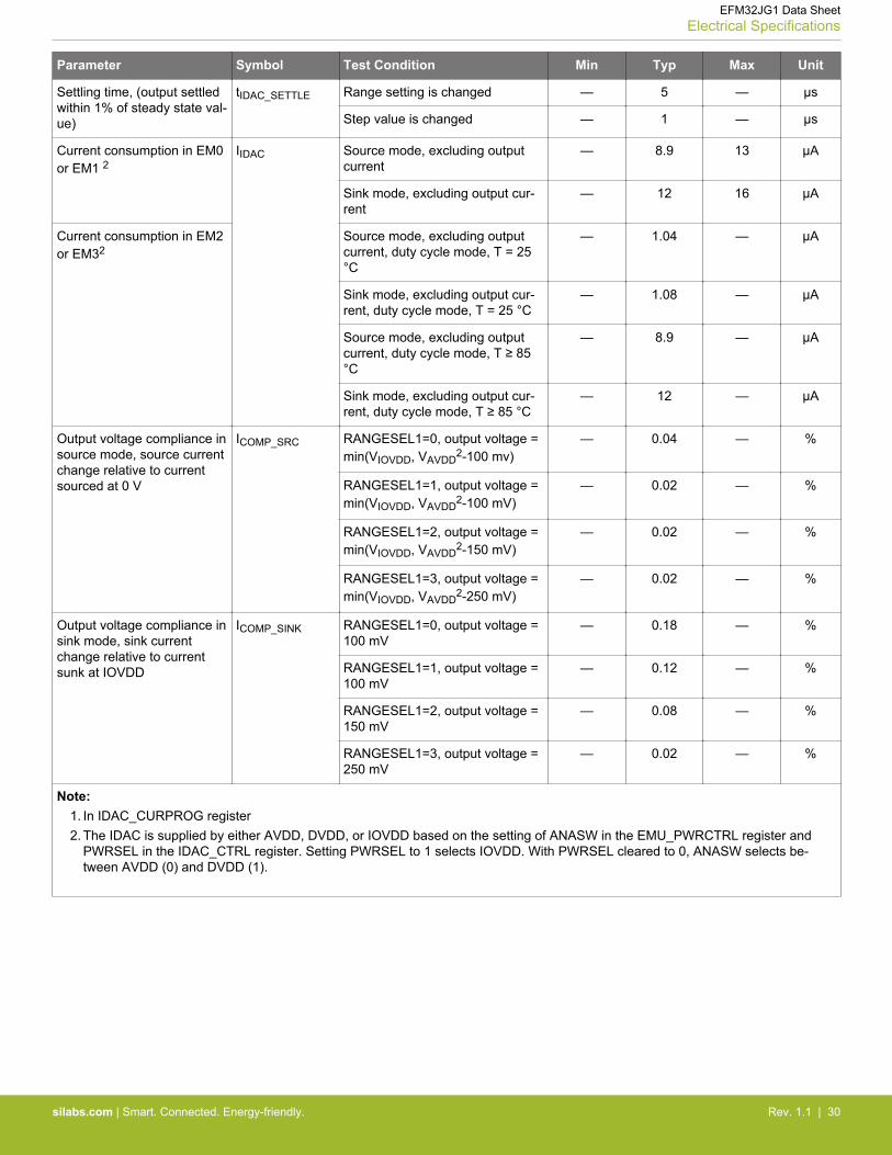
Parameter Symbol Test Condition Min Typ Max Unit
Settling time, (output settledwithin 1% of steady state val-ue)
tIDAC_SETTLE Range setting is changed — 5 — μs
Step value is changed — 1 — μs
Current consumption in EM0or EM1 2
IIDAC Source mode, excluding outputcurrent
— 8.9 13 μA
Sink mode, excluding output cur-rent
— 12 16 μA
Current consumption in EM2or EM32
Source mode, excluding outputcurrent, duty cycle mode, T = 25°C
— 1.04 — μA
Sink mode, excluding output cur-rent, duty cycle mode, T = 25 °C
— 1.08 — μA
Source mode, excluding outputcurrent, duty cycle mode, T ≥ 85°C
— 8.9 — μA
Sink mode, excluding output cur-rent, duty cycle mode, T ≥ 85 °C
— 12 — μA
Output voltage compliance insource mode, source currentchange relative to currentsourced at 0 V
ICOMP_SRC RANGESEL1=0, output voltage =min(VIOVDD, VAVDD
2-100 mv)— 0.04 — %
RANGESEL1=1, output voltage =min(VIOVDD, VAVDD
2-100 mV)— 0.02 — %
RANGESEL1=2, output voltage =min(VIOVDD, VAVDD
2-150 mV)— 0.02 — %
RANGESEL1=3, output voltage =min(VIOVDD, VAVDD
2-250 mV)— 0.02 — %
Output voltage compliance insink mode, sink currentchange relative to currentsunk at IOVDD
ICOMP_SINK RANGESEL1=0, output voltage =100 mV
— 0.18 — %
RANGESEL1=1, output voltage =100 mV
— 0.12 — %
RANGESEL1=2, output voltage =150 mV
— 0.08 — %
RANGESEL1=3, output voltage =250 mV
— 0.02 — %
Note:1. In IDAC_CURPROG register2. The IDAC is supplied by either AVDD, DVDD, or IOVDD based on the setting of ANASW in the EMU_PWRCTRL register and
PWRSEL in the IDAC_CTRL register. Setting PWRSEL to 1 selects IOVDD. With PWRSEL cleared to 0, ANASW selects be-tween AVDD (0) and DVDD (1).
EFM32JG1 Data SheetElectrical Specifications
silabs.com | Smart. Connected. Energy-friendly. Rev. 1.1 | 30
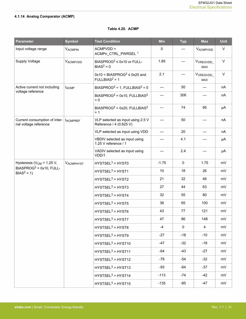
4.1.14 Analog Comparator (ACMP)
Table 4.20. ACMP
Parameter Symbol Test Condition Min Typ Max Unit
Input voltage range VACMPIN ACMPVDD =ACMPn_CTRL_PWRSEL 1
0 — VACMPVDD V
Supply Voltage VACMPVDD BIASPROG2 ≤ 0x10 or FULL-BIAS2 = 0
1.85 — VVREGVDD_
MAX
V
0x10 < BIASPROG2 ≤ 0x20 andFULLBIAS2 = 1
2.1 — VVREGVDD_
MAX
V
Active current not includingvoltage reference
IACMP BIASPROG2 = 1, FULLBIAS2 = 0 — 50 — nA
BIASPROG2 = 0x10, FULLBIAS2
= 0— 306 — nA
BIASPROG2 = 0x20, FULLBIAS2
= 1— 74 95 μA
Current consumption of inter-nal voltage reference
IACMPREF VLP selected as input using 2.5 VReference / 4 (0.625 V)
— 50 — nA
VLP selected as input using VDD — 20 — nA
VBDIV selected as input using1.25 V reference / 1
— 4.1 — μA
VADIV selected as input usingVDD/1
— 2.4 — μA
Hysteresis (VCM = 1.25 V,BIASPROG2 = 0x10, FULL-BIAS2 = 1)
VACMPHYST HYSTSEL3 = HYST0 -1.75 0 1.75 mV
HYSTSEL3 = HYST1 10 18 26 mV
HYSTSEL3 = HYST2 21 32 46 mV
HYSTSEL3 = HYST3 27 44 63 mV
HYSTSEL3 = HYST4 32 55 80 mV
HYSTSEL3 = HYST5 38 65 100 mV
HYSTSEL3 = HYST6 43 77 121 mV
HYSTSEL3 = HYST7 47 86 148 mV
HYSTSEL3 = HYST8 -4 0 4 mV
HYSTSEL3 = HYST9 -27 -18 -10 mV
HYSTSEL3 = HYST10 -47 -32 -18 mV
HYSTSEL3 = HYST11 -64 -43 -27 mV
HYSTSEL3 = HYST12 -78 -54 -32 mV
HYSTSEL3 = HYST13 -93 -64 -37 mV
HYSTSEL3 = HYST14 -113 -74 -42 mV
HYSTSEL3 = HYST15 -135 -85 -47 mV
EFM32JG1 Data SheetElectrical Specifications
silabs.com | Smart. Connected. Energy-friendly. Rev. 1.1 | 31

Parameter Symbol Test Condition Min Typ Max Unit
Comparator delay4 tACMPDELAY BIASPROG2 = 1, FULLBIAS2 = 0 — 30 — μs
BIASPROG2 = 0x10, FULLBIAS2
= 0— 3.7 — μs
BIASPROG2 = 0x20, FULLBIAS2
= 1— 35 — ns
Offset voltage VACMPOFFSET BIASPROG2 =0x10, FULLBIAS2
= 1-35 — 35 mV
Reference Voltage VACMPREF Internal 1.25 V reference 1 1.25 1.47 V
Internal 2.5 V reference 2 2.5 2.8 V
Capacitive Sense InternalResistance
RCSRES CSRESSEL5 = 0 — inf — kΩ
CSRESSEL5 = 1 — 15 — kΩ
CSRESSEL5 = 2 — 27 — kΩ
CSRESSEL5 = 3 — 39 — kΩ
CSRESSEL5 = 4 — 51 — kΩ
CSRESSEL5 = 5 — 102 — kΩ
CSRESSEL5 = 6 — 164 — kΩ
CSRESSEL5 = 7 — 239 — kΩ
Note:1. ACMPVDD is a supply chosen by the setting in ACMPn_CTRL_PWRSEL and may be IOVDD, AVDD or DVDD2. In ACMPn_CTRL register3. In ACMPn_HYSTERESIS register4. ±100 mV differential drive5. In ACMPn_INPUTSEL register
The total ACMP current is the sum of the contributions from the ACMP and its internal voltage reference as given as:
IACMPTOTAL = IACMP + IACMPREF
IACMPREF is zero if an external voltage reference is used.
EFM32JG1 Data SheetElectrical Specifications
silabs.com | Smart. Connected. Energy-friendly. Rev. 1.1 | 32

4.1.15 I2C
I2C Standard-mode (Sm)
Table 4.21. I2C Standard-mode (Sm)1
Parameter Symbol Test Condition Min Typ Max Unit
SCL clock frequency2 fSCL 0 — 100 kHz
SCL clock low time tLOW 4.7 — — μs
SCL clock high time tHIGH 4 — — μs
SDA set-up time tSU,DAT 250 — — ns
SDA hold time3 tHD,DAT 100 — 3450 ns
Repeated START conditionset-up time
tSU,STA 4.7 — — μs
(Repeated) START conditionhold time
tHD,STA 4 — — μs
STOP condition set-up time tSU,STO 4 — — μs
Bus free time between aSTOP and START condition
tBUF 4.7 — — μs
Note:1. For CLHR set to 0 in the I2Cn_CTRL register2. For the minimum HFPERCLK frequency required in Standard-mode, refer to the I2C chapter in the reference manual3. The maximum SDA hold time (tHD,DAT) needs to be met only when the device does not stretch the low time of SCL (tLOW)
EFM32JG1 Data SheetElectrical Specifications
silabs.com | Smart. Connected. Energy-friendly. Rev. 1.1 | 33
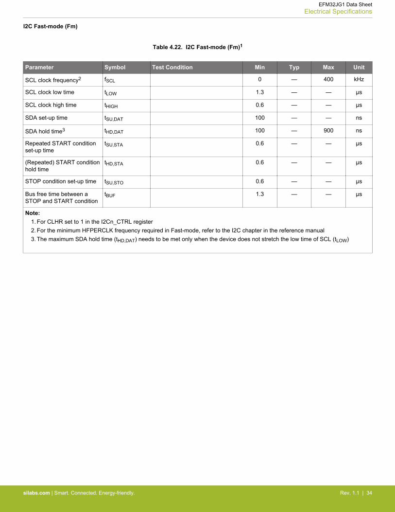
I2C Fast-mode (Fm)
Table 4.22. I2C Fast-mode (Fm)1
Parameter Symbol Test Condition Min Typ Max Unit
SCL clock frequency2 fSCL 0 — 400 kHz
SCL clock low time tLOW 1.3 — — μs
SCL clock high time tHIGH 0.6 — — μs
SDA set-up time tSU,DAT 100 — — ns
SDA hold time3 tHD,DAT 100 — 900 ns
Repeated START conditionset-up time
tSU,STA 0.6 — — μs
(Repeated) START conditionhold time
tHD,STA 0.6 — — μs
STOP condition set-up time tSU,STO 0.6 — — μs
Bus free time between aSTOP and START condition
tBUF 1.3 — — μs
Note:1. For CLHR set to 1 in the I2Cn_CTRL register2. For the minimum HFPERCLK frequency required in Fast-mode, refer to the I2C chapter in the reference manual3. The maximum SDA hold time (tHD,DAT) needs to be met only when the device does not stretch the low time of SCL (tLOW)
EFM32JG1 Data SheetElectrical Specifications
silabs.com | Smart. Connected. Energy-friendly. Rev. 1.1 | 34

I2C Fast-mode Plus (Fm+)
Table 4.23. I2C Fast-mode Plus (Fm+)1
Parameter Symbol Test Condition Min Typ Max Unit
SCL clock frequency2 fSCL 0 — 1000 kHz
SCL clock low time tLOW 0.5 — — μs
SCL clock high time tHIGH 0.26 — — μs
SDA set-up time tSU,DAT 50 — — ns
SDA hold time tHD,DAT 100 — — ns
Repeated START conditionset-up time
tSU,STA 0.26 — — μs
(Repeated) START conditionhold time
tHD,STA 0.26 — — μs
STOP condition set-up time tSU,STO 0.26 — — μs
Bus free time between aSTOP and START condition
tBUF 0.5 — — μs
Note:1. For CLHR set to 0 or 1 in the I2Cn_CTRL register2. For the minimum HFPERCLK frequency required in Fast-mode Plus, refer to the I2C chapter in the reference manual
EFM32JG1 Data SheetElectrical Specifications
silabs.com | Smart. Connected. Energy-friendly. Rev. 1.1 | 35
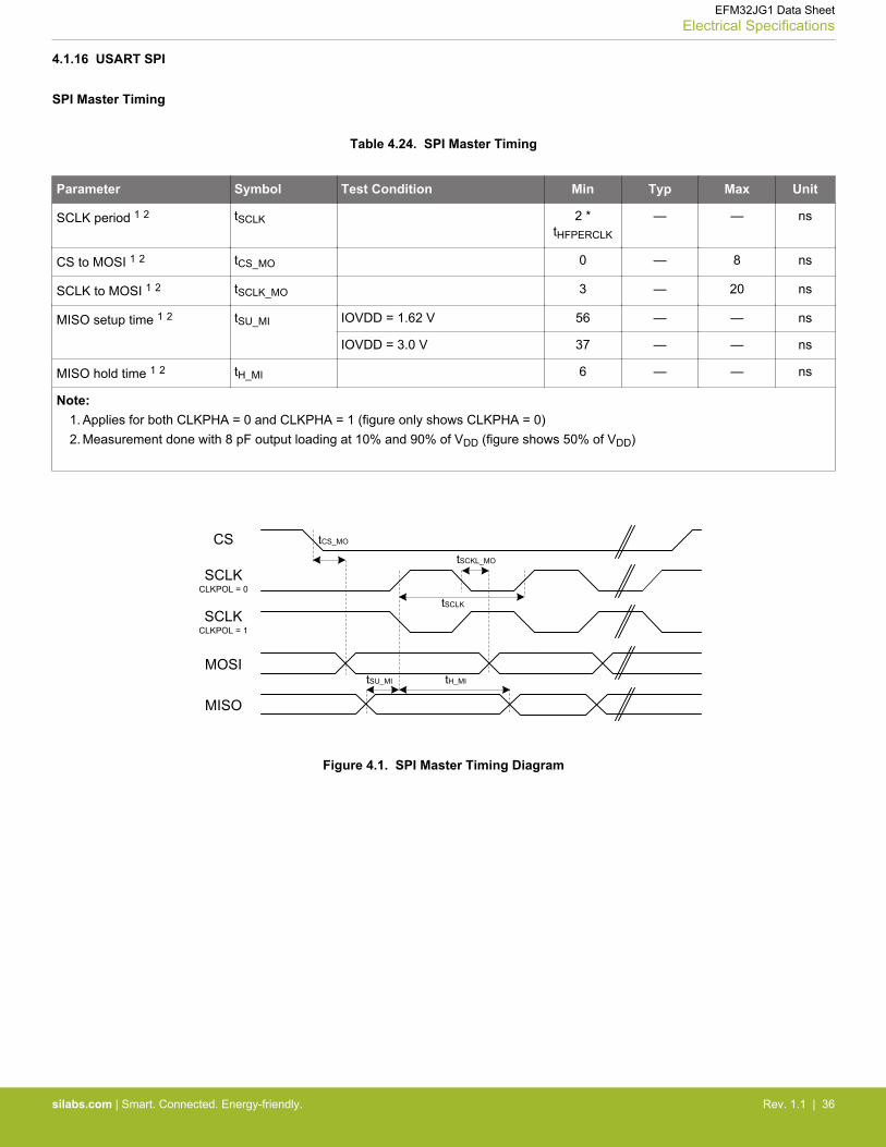
4.1.16 USART SPI
SPI Master Timing
Table 4.24. SPI Master Timing
Parameter Symbol Test Condition Min Typ Max Unit
SCLK period 1 2 tSCLK 2 *tHFPERCLK
— — ns
CS to MOSI 1 2 tCS_MO 0 — 8 ns
SCLK to MOSI 1 2 tSCLK_MO 3 — 20 ns
MISO setup time 1 2 tSU_MI IOVDD = 1.62 V 56 — — ns
IOVDD = 3.0 V 37 — — ns
MISO hold time 1 2 tH_MI 6 — — ns
Note:1. Applies for both CLKPHA = 0 and CLKPHA = 1 (figure only shows CLKPHA = 0)2. Measurement done with 8 pF output loading at 10% and 90% of VDD (figure shows 50% of VDD)
CS
SCLKCLKPOL = 0
MOSI
MISO
tCS_MO
tH_MItSU_MI
tSCKL_MO
tSCLK
SCLKCLKPOL = 1
Figure 4.1. SPI Master Timing Diagram
EFM32JG1 Data SheetElectrical Specifications
silabs.com | Smart. Connected. Energy-friendly. Rev. 1.1 | 36
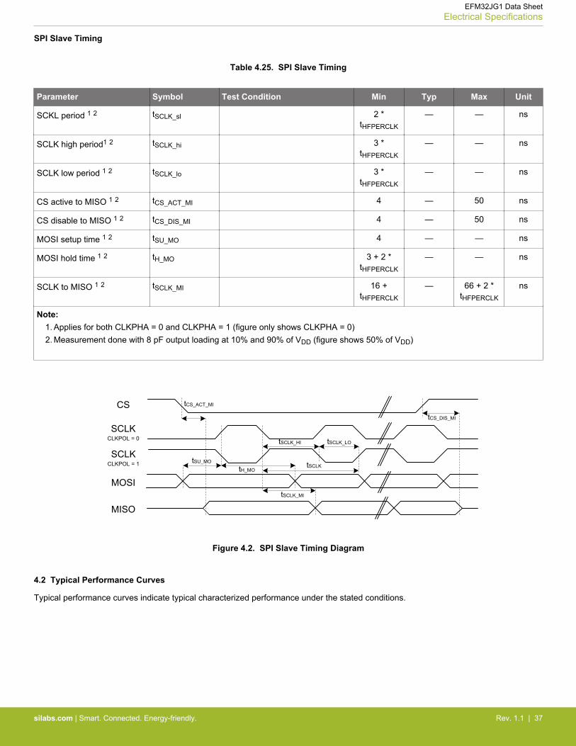
SPI Slave Timing
Table 4.25. SPI Slave Timing
Parameter Symbol Test Condition Min Typ Max Unit
SCKL period 1 2 tSCLK_sl 2 *tHFPERCLK
— — ns
SCLK high period1 2 tSCLK_hi 3 *tHFPERCLK
— — ns
SCLK low period 1 2 tSCLK_lo 3 *tHFPERCLK
— — ns
CS active to MISO 1 2 tCS_ACT_MI 4 — 50 ns
CS disable to MISO 1 2 tCS_DIS_MI 4 — 50 ns
MOSI setup time 1 2 tSU_MO 4 — — ns
MOSI hold time 1 2 tH_MO 3 + 2 *tHFPERCLK
— — ns
SCLK to MISO 1 2 tSCLK_MI 16 +tHFPERCLK
— 66 + 2 *tHFPERCLK
ns
Note:1. Applies for both CLKPHA = 0 and CLKPHA = 1 (figure only shows CLKPHA = 0)2. Measurement done with 8 pF output loading at 10% and 90% of VDD (figure shows 50% of VDD)
CS
SCLKCLKPOL = 0
MOSI
MISO
tCS_ACT_MI
tSCLK_HI
tSCLKtSU_MO
tH_MO
tSCLK_MI
tCS_DIS_MI
tSCLK_LO
SCLKCLKPOL = 1
Figure 4.2. SPI Slave Timing Diagram
4.2 Typical Performance Curves
Typical performance curves indicate typical characterized performance under the stated conditions.
EFM32JG1 Data SheetElectrical Specifications
silabs.com | Smart. Connected. Energy-friendly. Rev. 1.1 | 37

4.2.1 Supply Current
Figure 4.3. EM0 Active Mode Typical Supply Current
Figure 4.4. EM1 Sleep Mode Typical Supply Current
Typical supply current for EM2, EM3 and EM4H using standard software libraries from Silicon Laboratories.
EFM32JG1 Data SheetElectrical Specifications
silabs.com | Smart. Connected. Energy-friendly. Rev. 1.1 | 38
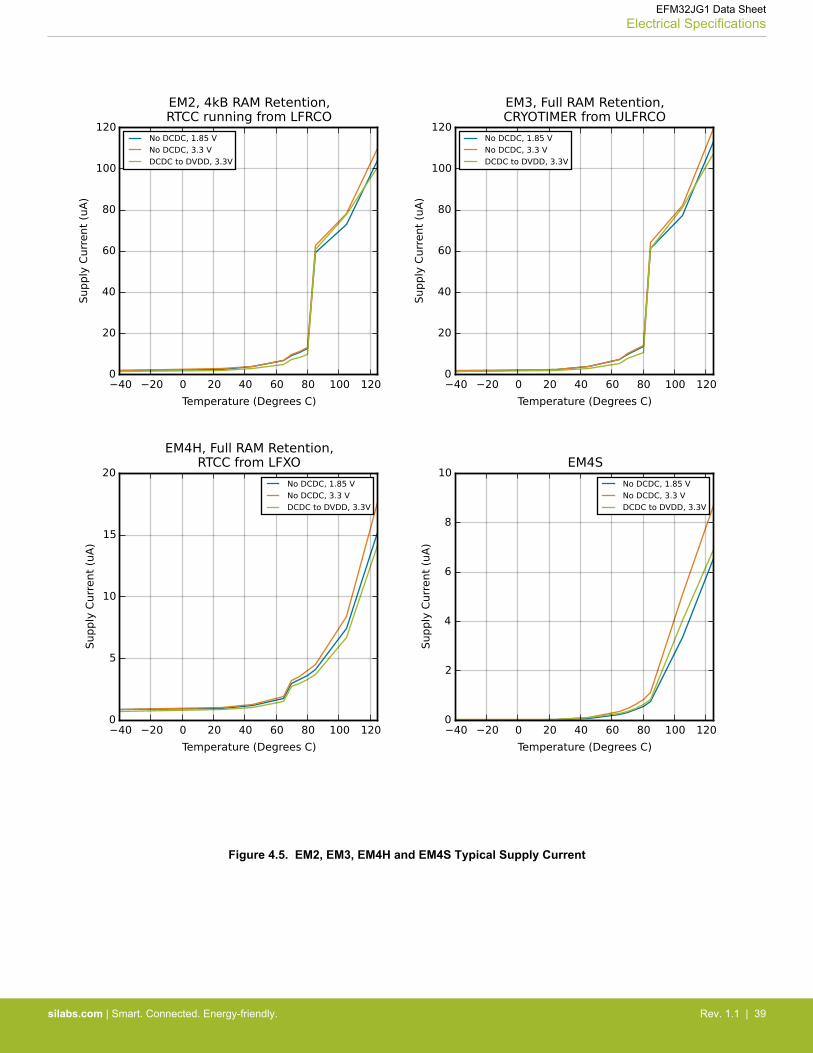
Figure 4.5. EM2, EM3, EM4H and EM4S Typical Supply Current
EFM32JG1 Data SheetElectrical Specifications
silabs.com | Smart. Connected. Energy-friendly. Rev. 1.1 | 39
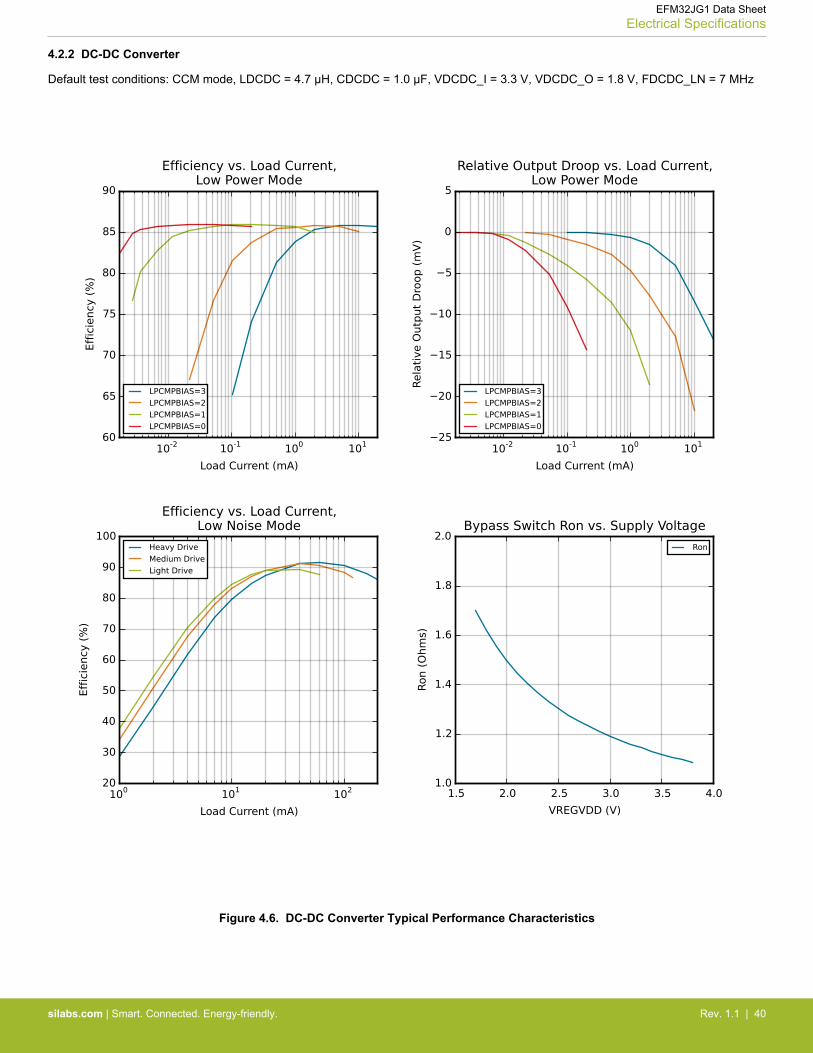
4.2.2 DC-DC Converter
Default test conditions: CCM mode, LDCDC = 4.7 μH, CDCDC = 1.0 μF, VDCDC_I = 3.3 V, VDCDC_O = 1.8 V, FDCDC_LN = 7 MHz
Figure 4.6. DC-DC Converter Typical Performance Characteristics
EFM32JG1 Data SheetElectrical Specifications
silabs.com | Smart. Connected. Energy-friendly. Rev. 1.1 | 40

100μs/div 10μs/div
2V/div offset:1.8V
50mV/div offset:1.8V
100mA
1mAILOAD
60mV/div offset:1.8V
VSW
DVDDDVDD
Load Step Response in LN (CCM) mode(Heavy Drive)LN (CCM) and LP mode transition (load: 5mA)
Figure 4.7. DC-DC Converter Transition Waveforms
EFM32JG1 Data SheetElectrical Specifications
silabs.com | Smart. Connected. Energy-friendly. Rev. 1.1 | 41
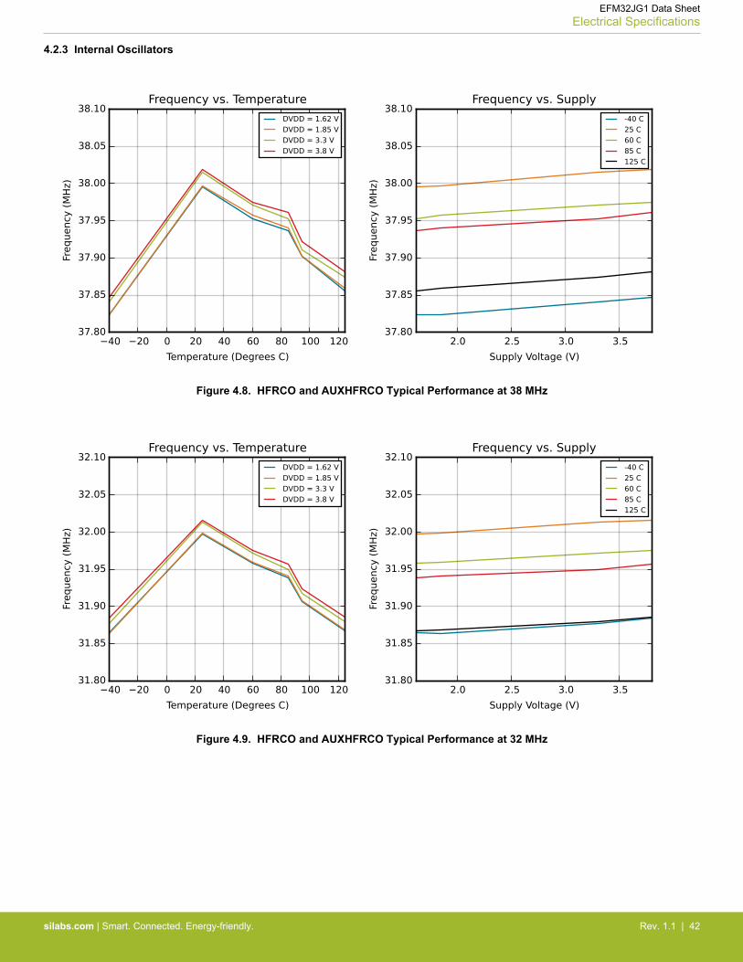
4.2.3 Internal Oscillators
Figure 4.8. HFRCO and AUXHFRCO Typical Performance at 38 MHz
Figure 4.9. HFRCO and AUXHFRCO Typical Performance at 32 MHz
EFM32JG1 Data SheetElectrical Specifications
silabs.com | Smart. Connected. Energy-friendly. Rev. 1.1 | 42

Figure 4.10. HFRCO and AUXHFRCO Typical Performance at 26 MHz
Figure 4.11. HFRCO and AUXHFRCO Typical Performance at 19 MHz
EFM32JG1 Data SheetElectrical Specifications
silabs.com | Smart. Connected. Energy-friendly. Rev. 1.1 | 43

Figure 4.12. HFRCO and AUXHFRCO Typical Performance at 16 MHz
Figure 4.13. HFRCO and AUXHFRCO Typical Performance at 13 MHz
EFM32JG1 Data SheetElectrical Specifications
silabs.com | Smart. Connected. Energy-friendly. Rev. 1.1 | 44

Figure 4.14. HFRCO and AUXHFRCO Typical Performance at 7 MHz
Figure 4.15. HFRCO and AUXHFRCO Typical Performance at 4 MHz
EFM32JG1 Data SheetElectrical Specifications
silabs.com | Smart. Connected. Energy-friendly. Rev. 1.1 | 45
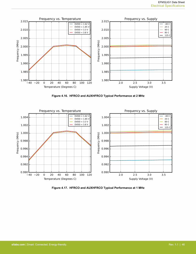
Figure 4.16. HFRCO and AUXHFRCO Typical Performance at 2 MHz
Figure 4.17. HFRCO and AUXHFRCO Typical Performance at 1 MHz
EFM32JG1 Data SheetElectrical Specifications
silabs.com | Smart. Connected. Energy-friendly. Rev. 1.1 | 46
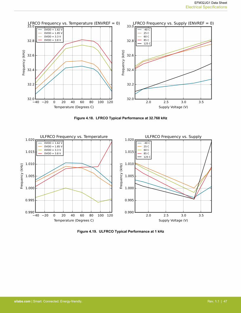
Figure 4.18. LFRCO Typical Performance at 32.768 kHz
Figure 4.19. ULFRCO Typical Performance at 1 kHz
EFM32JG1 Data SheetElectrical Specifications
silabs.com | Smart. Connected. Energy-friendly. Rev. 1.1 | 47
5. Typical Connection Diagrams
5.1 Power
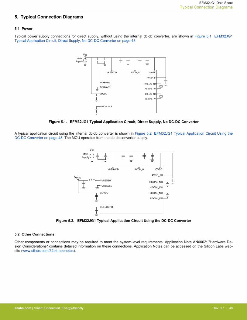
Typical power supply connections for direct supply, without using the internal dc-dc converter, are shown in Figure 5.1 EFM32JG1Typical Application Circuit, Direct Supply, No DC-DC Converter on page 48.
MainSupply
VDD
VREGVDD AVDD_0 IOVDD
VREGSW
VREGVSS
DVDD
DECOUPLE
HFXTAL_N
HFXTAL_P
LFXTAL_N
LFXTAL_P
+–
AVDD_1
Figure 5.1. EFM32JG1 Typical Application Circuit, Direct Supply, No DC-DC Converter
A typical application circuit using the internal dc-dc converter is shown in Figure 5.2 EFM32JG1 Typical Application Circuit Using theDC-DC Converter on page 48. The MCU operates from the dc-dc converter supply.
MainSupply
VDCDC
VDD
VREGVDD AVDD_0 IOVDD
VREGSW
VREGVSS
DVDD
DECOUPLE
HFXTAL_N
HFXTAL_P
LFXTAL_N
LFXTAL_P
+–
AVDD_1
Figure 5.2. EFM32JG1 Typical Application Circuit Using the DC-DC Converter
5.2 Other Connections
Other components or connections may be required to meet the system-level requirements. Application Note AN0002: "Hardware De-sign Considerations" contains detailed information on these connections. Application Notes can be accessed on the Silicon Labs web-site (www.silabs.com/32bit-appnotes).
EFM32JG1 Data SheetTypical Connection Diagrams
silabs.com | Smart. Connected. Energy-friendly. Rev. 1.1 | 48
6. Pin Definitions
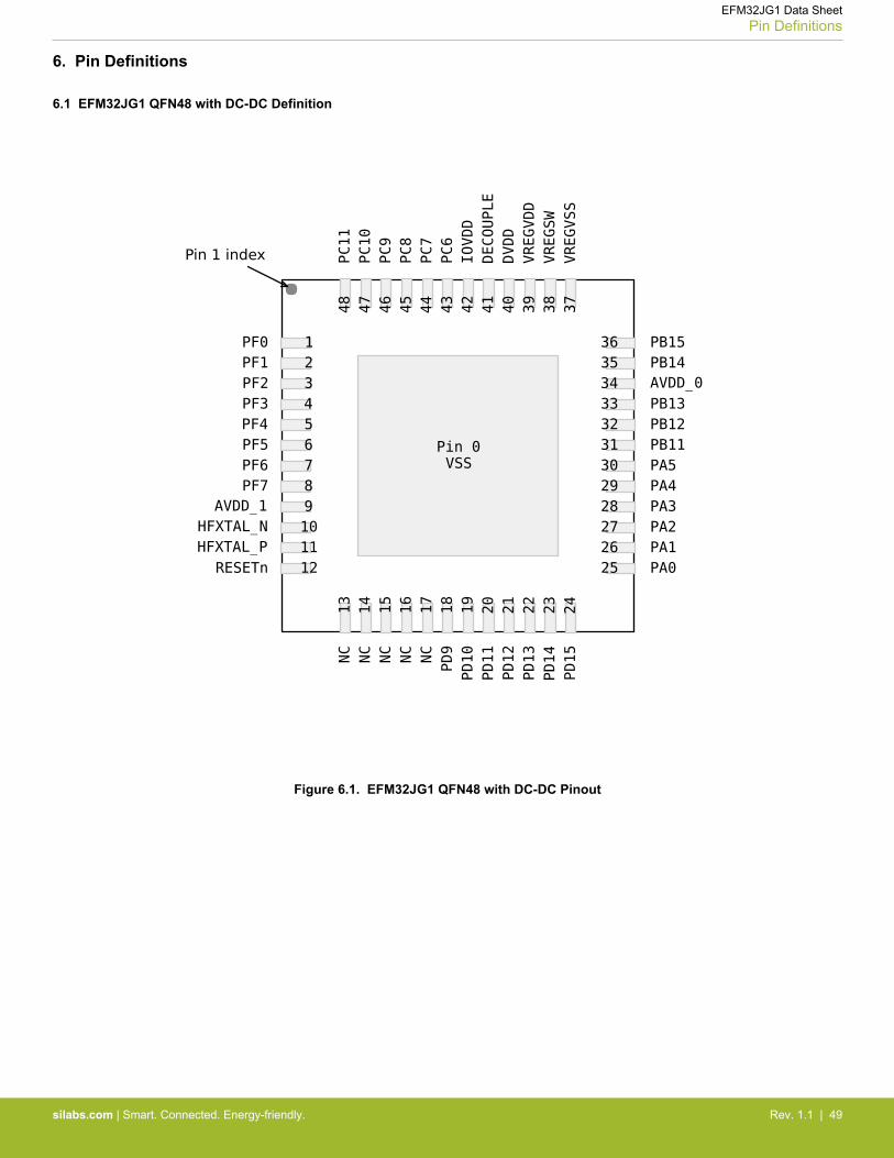
6.1 EFM32JG1 QFN48 with DC-DC Definition
Figure 6.1. EFM32JG1 QFN48 with DC-DC Pinout
EFM32JG1 Data SheetPin Definitions
silabs.com | Smart. Connected. Energy-friendly. Rev. 1.1 | 49
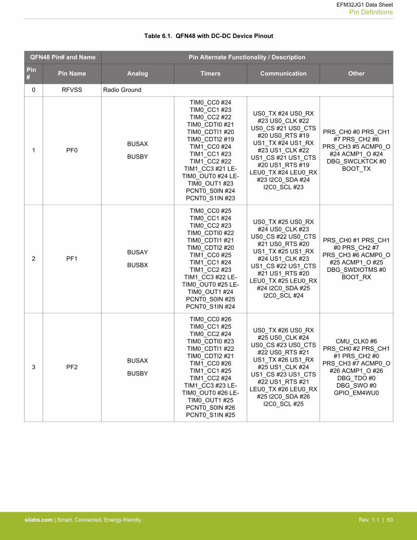
Table 6.1. QFN48 with DC-DC Device Pinout
QFN48 Pin# and Name Pin Alternate Functionality / Description
Pin# Pin Name Analog Timers Communication Other
0 RFVSS Radio Ground
1 PF0BUSAX
BUSBY
TIM0_CC0 #24TIM0_CC1 #23TIM0_CC2 #22
TIM0_CDTI0 #21TIM0_CDTI1 #20TIM0_CDTI2 #19TIM1_CC0 #24TIM1_CC1 #23TIM1_CC2 #22
TIM1_CC3 #21 LE-TIM0_OUT0 #24 LE-
TIM0_OUT1 #23PCNT0_S0IN #24PCNT0_S1IN #23
US0_TX #24 US0_RX#23 US0_CLK #22
US0_CS #21 US0_CTS#20 US0_RTS #19
US1_TX #24 US1_RX#23 US1_CLK #22
US1_CS #21 US1_CTS#20 US1_RTS #19
LEU0_TX #24 LEU0_RX#23 I2C0_SDA #24
I2C0_SCL #23
PRS_CH0 #0 PRS_CH1#7 PRS_CH2 #6
PRS_CH3 #5 ACMP0_O#24 ACMP1_O #24
DBG_SWCLKTCK #0BOOT_TX
2 PF1BUSAY
BUSBX
TIM0_CC0 #25TIM0_CC1 #24TIM0_CC2 #23
TIM0_CDTI0 #22TIM0_CDTI1 #21TIM0_CDTI2 #20TIM1_CC0 #25TIM1_CC1 #24TIM1_CC2 #23
TIM1_CC3 #22 LE-TIM0_OUT0 #25 LE-
TIM0_OUT1 #24PCNT0_S0IN #25PCNT0_S1IN #24
US0_TX #25 US0_RX#24 US0_CLK #23
US0_CS #22 US0_CTS#21 US0_RTS #20
US1_TX #25 US1_RX#24 US1_CLK #23
US1_CS #22 US1_CTS#21 US1_RTS #20
LEU0_TX #25 LEU0_RX#24 I2C0_SDA #25
I2C0_SCL #24
PRS_CH0 #1 PRS_CH1#0 PRS_CH2 #7
PRS_CH3 #6 ACMP0_O#25 ACMP1_O #25
DBG_SWDIOTMS #0BOOT_RX
3 PF2BUSAX
BUSBY
TIM0_CC0 #26TIM0_CC1 #25TIM0_CC2 #24
TIM0_CDTI0 #23TIM0_CDTI1 #22TIM0_CDTI2 #21TIM1_CC0 #26TIM1_CC1 #25TIM1_CC2 #24
TIM1_CC3 #23 LE-TIM0_OUT0 #26 LE-
TIM0_OUT1 #25PCNT0_S0IN #26PCNT0_S1IN #25
US0_TX #26 US0_RX#25 US0_CLK #24
US0_CS #23 US0_CTS#22 US0_RTS #21
US1_TX #26 US1_RX#25 US1_CLK #24
US1_CS #23 US1_CTS#22 US1_RTS #21
LEU0_TX #26 LEU0_RX#25 I2C0_SDA #26
I2C0_SCL #25
CMU_CLK0 #6PRS_CH0 #2 PRS_CH1
#1 PRS_CH2 #0PRS_CH3 #7 ACMP0_O
#26 ACMP1_O #26DBG_TDO #0DBG_SWO #0
GPIO_EM4WU0
EFM32JG1 Data SheetPin Definitions
silabs.com | Smart. Connected. Energy-friendly. Rev. 1.1 | 50

QFN48 Pin# and Name Pin Alternate Functionality / Description
Pin# Pin Name Analog Timers Communication Other
4 PF3BUSAY
BUSBX
TIM0_CC0 #27TIM0_CC1 #26TIM0_CC2 #25
TIM0_CDTI0 #24TIM0_CDTI1 #23TIM0_CDTI2 #22TIM1_CC0 #27TIM1_CC1 #26TIM1_CC2 #25
TIM1_CC3 #24 LE-TIM0_OUT0 #27 LE-
TIM0_OUT1 #26PCNT0_S0IN #27PCNT0_S1IN #26
US0_TX #27 US0_RX#26 US0_CLK #25
US0_CS #24 US0_CTS#23 US0_RTS #22
US1_TX #27 US1_RX#26 US1_CLK #25
US1_CS #24 US1_CTS#23 US1_RTS #22
LEU0_TX #27 LEU0_RX#26 I2C0_SDA #27
I2C0_SCL #26
CMU_CLK1 #6PRS_CH0 #3 PRS_CH1
#2 PRS_CH2 #1PRS_CH3 #0 ACMP0_O
#27 ACMP1_O #27DBG_TDI #0
5 PF4BUSAX
BUSBY
TIM0_CC0 #28TIM0_CC1 #27TIM0_CC2 #26
TIM0_CDTI0 #25TIM0_CDTI1 #24TIM0_CDTI2 #23TIM1_CC0 #28TIM1_CC1 #27TIM1_CC2 #26
TIM1_CC3 #25 LE-TIM0_OUT0 #28 LE-
TIM0_OUT1 #27PCNT0_S0IN #28PCNT0_S1IN #27
US0_TX #28 US0_RX#27 US0_CLK #26
US0_CS #25 US0_CTS#24 US0_RTS #23
US1_TX #28 US1_RX#27 US1_CLK #26
US1_CS #25 US1_CTS#24 US1_RTS #23
LEU0_TX #28 LEU0_RX#27 I2C0_SDA #28
I2C0_SCL #27
PRS_CH0 #4 PRS_CH1#3 PRS_CH2 #2
PRS_CH3 #1 ACMP0_O#28 ACMP1_O #28
6 PF5BUSAY
BUSBX
TIM0_CC0 #29TIM0_CC1 #28TIM0_CC2 #27
TIM0_CDTI0 #26TIM0_CDTI1 #25TIM0_CDTI2 #24TIM1_CC0 #29TIM1_CC1 #28TIM1_CC2 #27
TIM1_CC3 #26 LE-TIM0_OUT0 #29 LE-
TIM0_OUT1 #28PCNT0_S0IN #29PCNT0_S1IN #28
US0_TX #29 US0_RX#28 US0_CLK #27
US0_CS #26 US0_CTS#25 US0_RTS #24
US1_TX #29 US1_RX#28 US1_CLK #27
US1_CS #26 US1_CTS#25 US1_RTS #24
LEU0_TX #29 LEU0_RX#28 I2C0_SDA #29
I2C0_SCL #28
PRS_CH0 #5 PRS_CH1#4 PRS_CH2 #3
PRS_CH3 #2 ACMP0_O#29 ACMP1_O #29
7 PF6BUSAX
BUSBY
TIM0_CC0 #30TIM0_CC1 #29TIM0_CC2 #28
TIM0_CDTI0 #27TIM0_CDTI1 #26TIM0_CDTI2 #25TIM1_CC0 #30TIM1_CC1 #29TIM1_CC2 #28
TIM1_CC3 #27 LE-TIM0_OUT0 #30 LE-
TIM0_OUT1 #29PCNT0_S0IN #30PCNT0_S1IN #29
US0_TX #30 US0_RX#29 US0_CLK #28
US0_CS #27 US0_CTS#26 US0_RTS #25
US1_TX #30 US1_RX#29 US1_CLK #28
US1_CS #27 US1_CTS#26 US1_RTS #25
LEU0_TX #30 LEU0_RX#29 I2C0_SDA #30
I2C0_SCL #29
CMU_CLK1 #7PRS_CH0 #6 PRS_CH1
#5 PRS_CH2 #4PRS_CH3 #3 ACMP0_O
#30 ACMP1_O #30
EFM32JG1 Data SheetPin Definitions
silabs.com | Smart. Connected. Energy-friendly. Rev. 1.1 | 51

QFN48 Pin# and Name Pin Alternate Functionality / Description
Pin# Pin Name Analog Timers Communication Other
8 PF7BUSAY
BUSBX
TIM0_CC0 #31TIM0_CC1 #30TIM0_CC2 #29
TIM0_CDTI0 #28TIM0_CDTI1 #27TIM0_CDTI2 #26TIM1_CC0 #31TIM1_CC1 #30TIM1_CC2 #29
TIM1_CC3 #28 LE-TIM0_OUT0 #31 LE-
TIM0_OUT1 #30PCNT0_S0IN #31PCNT0_S1IN #30
US0_TX #31 US0_RX#30 US0_CLK #29
US0_CS #28 US0_CTS#27 US0_RTS #26
US1_TX #31 US1_RX#30 US1_CLK #29
US1_CS #28 US1_CTS#27 US1_RTS #26
LEU0_TX #31 LEU0_RX#30 I2C0_SDA #31
I2C0_SCL #30
CMU_CLK0 #7PRS_CH0 #7 PRS_CH1
#6 PRS_CH2 #5PRS_CH3 #4 ACMP0_O
#31 ACMP1_O #31GPIO_EM4WU1
9 AVDD Analog power supply .
10 HFXTAL_N High Frequency Crystal input pin.
11 HFXTAL_P High Frequency Crystal output pin.
12 RESETn Reset input, active low.To apply an external reset source to this pin, it is required to only drive this pin lowduring reset, and let the internal pull-up ensure that reset is released.
13 NC No Connect.
14 NC No Connect.
15 NC No Connect.
16 NC No Connect.
17 NC No Connect.
18 PD9BUSCY
BUSDX
TIM0_CC0 #17TIM0_CC1 #16TIM0_CC2 #15
TIM0_CDTI0 #14TIM0_CDTI1 #13TIM0_CDTI2 #12TIM1_CC0 #17TIM1_CC1 #16TIM1_CC2 #15
TIM1_CC3 #14 LE-TIM0_OUT0 #17 LE-
TIM0_OUT1 #16PCNT0_S0IN #17PCNT0_S1IN #16
US0_TX #17 US0_RX#16 US0_CLK #15
US0_CS #14 US0_CTS#13 US0_RTS #12
US1_TX #17 US1_RX#16 US1_CLK #15
US1_CS #14 US1_CTS#13 US1_RTS #12
LEU0_TX #17 LEU0_RX#16 I2C0_SDA #17
I2C0_SCL #16
CMU_CLK0 #4PRS_CH3 #8 PRS_CH4
#0 PRS_CH5 #6PRS_CH6 #11ACMP0_O #17ACMP1_O #17
19 PD10BUSCX
BUSDY
TIM0_CC0 #18TIM0_CC1 #17TIM0_CC2 #16
TIM0_CDTI0 #15TIM0_CDTI1 #14TIM0_CDTI2 #13TIM1_CC0 #18TIM1_CC1 #17TIM1_CC2 #16
TIM1_CC3 #15 LE-TIM0_OUT0 #18 LE-
TIM0_OUT1 #17PCNT0_S0IN #18PCNT0_S1IN #17
US0_TX #18 US0_RX#17 US0_CLK #16
US0_CS #15 US0_CTS#14 US0_RTS #13
US1_TX #18 US1_RX#17 US1_CLK #16
US1_CS #15 US1_CTS#14 US1_RTS #13
LEU0_TX #18 LEU0_RX#17 I2C0_SDA #18
I2C0_SCL #17
CMU_CLK1 #4PRS_CH3 #9 PRS_CH4
#1 PRS_CH5 #0PRS_CH6 #12ACMP0_O #18ACMP1_O #18
EFM32JG1 Data SheetPin Definitions
silabs.com | Smart. Connected. Energy-friendly. Rev. 1.1 | 52
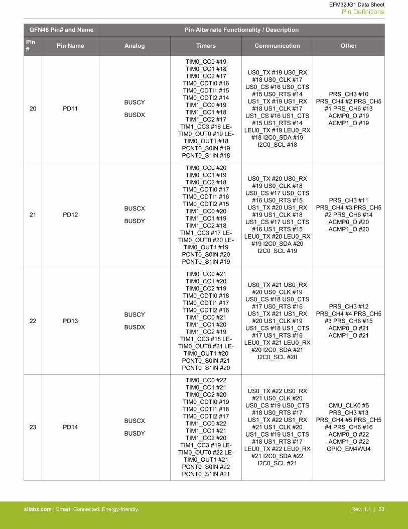
QFN48 Pin# and Name Pin Alternate Functionality / Description
Pin# Pin Name Analog Timers Communication Other
20 PD11BUSCY
BUSDX
TIM0_CC0 #19TIM0_CC1 #18TIM0_CC2 #17
TIM0_CDTI0 #16TIM0_CDTI1 #15TIM0_CDTI2 #14TIM1_CC0 #19TIM1_CC1 #18TIM1_CC2 #17
TIM1_CC3 #16 LE-TIM0_OUT0 #19 LE-
TIM0_OUT1 #18PCNT0_S0IN #19PCNT0_S1IN #18
US0_TX #19 US0_RX#18 US0_CLK #17
US0_CS #16 US0_CTS#15 US0_RTS #14
US1_TX #19 US1_RX#18 US1_CLK #17
US1_CS #16 US1_CTS#15 US1_RTS #14
LEU0_TX #19 LEU0_RX#18 I2C0_SDA #19
I2C0_SCL #18
PRS_CH3 #10PRS_CH4 #2 PRS_CH5
#1 PRS_CH6 #13ACMP0_O #19ACMP1_O #19
21 PD12BUSCX
BUSDY
TIM0_CC0 #20TIM0_CC1 #19TIM0_CC2 #18
TIM0_CDTI0 #17TIM0_CDTI1 #16TIM0_CDTI2 #15TIM1_CC0 #20TIM1_CC1 #19TIM1_CC2 #18
TIM1_CC3 #17 LE-TIM0_OUT0 #20 LE-
TIM0_OUT1 #19PCNT0_S0IN #20PCNT0_S1IN #19
US0_TX #20 US0_RX#19 US0_CLK #18
US0_CS #17 US0_CTS#16 US0_RTS #15
US1_TX #20 US1_RX#19 US1_CLK #18
US1_CS #17 US1_CTS#16 US1_RTS #15
LEU0_TX #20 LEU0_RX#19 I2C0_SDA #20
I2C0_SCL #19
PRS_CH3 #11PRS_CH4 #3 PRS_CH5
#2 PRS_CH6 #14ACMP0_O #20ACMP1_O #20
22 PD13BUSCY
BUSDX
TIM0_CC0 #21TIM0_CC1 #20TIM0_CC2 #19
TIM0_CDTI0 #18TIM0_CDTI1 #17TIM0_CDTI2 #16TIM1_CC0 #21TIM1_CC1 #20TIM1_CC2 #19
TIM1_CC3 #18 LE-TIM0_OUT0 #21 LE-
TIM0_OUT1 #20PCNT0_S0IN #21PCNT0_S1IN #20
US0_TX #21 US0_RX#20 US0_CLK #19
US0_CS #18 US0_CTS#17 US0_RTS #16
US1_TX #21 US1_RX#20 US1_CLK #19
US1_CS #18 US1_CTS#17 US1_RTS #16
LEU0_TX #21 LEU0_RX#20 I2C0_SDA #21
I2C0_SCL #20
PRS_CH3 #12PRS_CH4 #4 PRS_CH5
#3 PRS_CH6 #15ACMP0_O #21ACMP1_O #21
23 PD14BUSCX
BUSDY
TIM0_CC0 #22TIM0_CC1 #21TIM0_CC2 #20
TIM0_CDTI0 #19TIM0_CDTI1 #18TIM0_CDTI2 #17TIM1_CC0 #22TIM1_CC1 #21TIM1_CC2 #20
TIM1_CC3 #19 LE-TIM0_OUT0 #22 LE-
TIM0_OUT1 #21PCNT0_S0IN #22PCNT0_S1IN #21
US0_TX #22 US0_RX#21 US0_CLK #20
US0_CS #19 US0_CTS#18 US0_RTS #17
US1_TX #22 US1_RX#21 US1_CLK #20
US1_CS #19 US1_CTS#18 US1_RTS #17
LEU0_TX #22 LEU0_RX#21 I2C0_SDA #22
I2C0_SCL #21
CMU_CLK0 #5PRS_CH3 #13
PRS_CH4 #5 PRS_CH5#4 PRS_CH6 #16
ACMP0_O #22ACMP1_O #22
GPIO_EM4WU4
EFM32JG1 Data SheetPin Definitions
silabs.com | Smart. Connected. Energy-friendly. Rev. 1.1 | 53
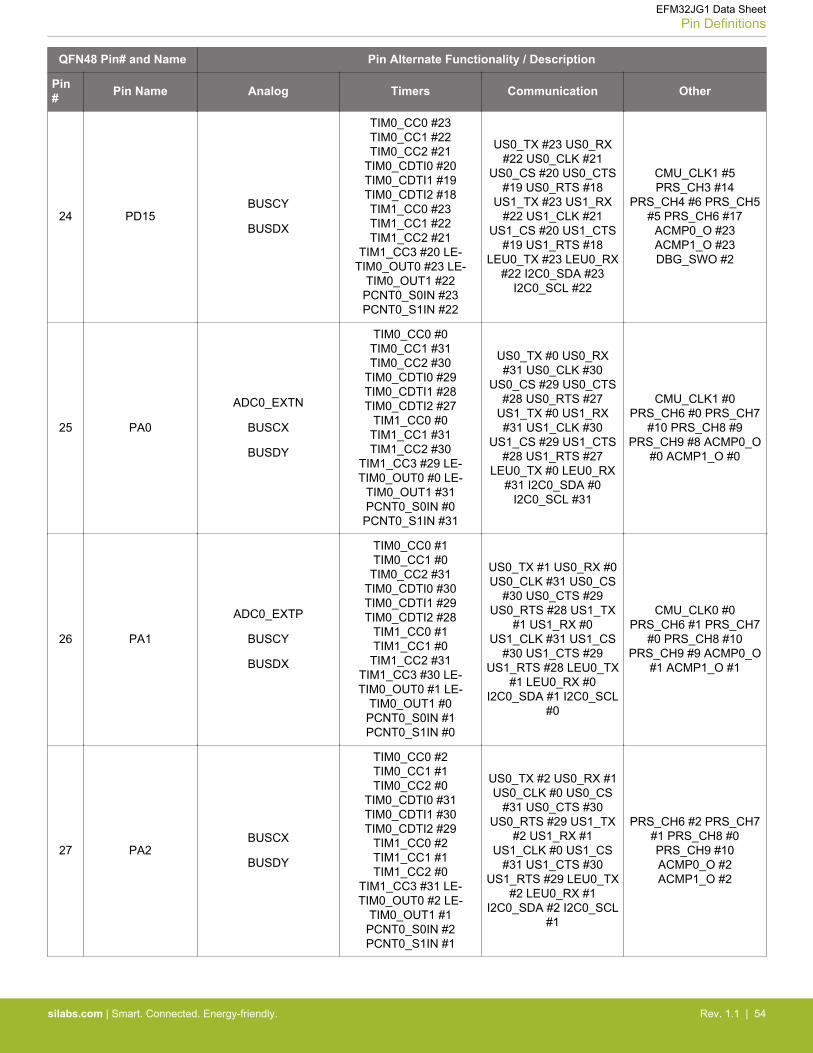
QFN48 Pin# and Name Pin Alternate Functionality / Description
Pin# Pin Name Analog Timers Communication Other
24 PD15BUSCY
BUSDX
TIM0_CC0 #23TIM0_CC1 #22TIM0_CC2 #21
TIM0_CDTI0 #20TIM0_CDTI1 #19TIM0_CDTI2 #18TIM1_CC0 #23TIM1_CC1 #22TIM1_CC2 #21
TIM1_CC3 #20 LE-TIM0_OUT0 #23 LE-
TIM0_OUT1 #22PCNT0_S0IN #23PCNT0_S1IN #22
US0_TX #23 US0_RX#22 US0_CLK #21
US0_CS #20 US0_CTS#19 US0_RTS #18
US1_TX #23 US1_RX#22 US1_CLK #21
US1_CS #20 US1_CTS#19 US1_RTS #18
LEU0_TX #23 LEU0_RX#22 I2C0_SDA #23
I2C0_SCL #22
CMU_CLK1 #5PRS_CH3 #14
PRS_CH4 #6 PRS_CH5#5 PRS_CH6 #17
ACMP0_O #23ACMP1_O #23DBG_SWO #2
25 PA0
ADC0_EXTN
BUSCX
BUSDY
TIM0_CC0 #0TIM0_CC1 #31TIM0_CC2 #30
TIM0_CDTI0 #29TIM0_CDTI1 #28TIM0_CDTI2 #27
TIM1_CC0 #0TIM1_CC1 #31TIM1_CC2 #30
TIM1_CC3 #29 LE-TIM0_OUT0 #0 LE-
TIM0_OUT1 #31PCNT0_S0IN #0
PCNT0_S1IN #31
US0_TX #0 US0_RX#31 US0_CLK #30
US0_CS #29 US0_CTS#28 US0_RTS #27
US1_TX #0 US1_RX#31 US1_CLK #30
US1_CS #29 US1_CTS#28 US1_RTS #27
LEU0_TX #0 LEU0_RX#31 I2C0_SDA #0
I2C0_SCL #31
CMU_CLK1 #0PRS_CH6 #0 PRS_CH7
#10 PRS_CH8 #9PRS_CH9 #8 ACMP0_O
#0 ACMP1_O #0
26 PA1
ADC0_EXTP
BUSCY
BUSDX
TIM0_CC0 #1TIM0_CC1 #0
TIM0_CC2 #31TIM0_CDTI0 #30TIM0_CDTI1 #29TIM0_CDTI2 #28
TIM1_CC0 #1TIM1_CC1 #0
TIM1_CC2 #31TIM1_CC3 #30 LE-TIM0_OUT0 #1 LE-
TIM0_OUT1 #0PCNT0_S0IN #1PCNT0_S1IN #0
US0_TX #1 US0_RX #0US0_CLK #31 US0_CS
#30 US0_CTS #29US0_RTS #28 US1_TX
#1 US1_RX #0US1_CLK #31 US1_CS
#30 US1_CTS #29US1_RTS #28 LEU0_TX
#1 LEU0_RX #0I2C0_SDA #1 I2C0_SCL
#0
CMU_CLK0 #0PRS_CH6 #1 PRS_CH7
#0 PRS_CH8 #10PRS_CH9 #9 ACMP0_O
#1 ACMP1_O #1
27 PA2BUSCX
BUSDY
TIM0_CC0 #2TIM0_CC1 #1TIM0_CC2 #0
TIM0_CDTI0 #31TIM0_CDTI1 #30TIM0_CDTI2 #29
TIM1_CC0 #2TIM1_CC1 #1TIM1_CC2 #0
TIM1_CC3 #31 LE-TIM0_OUT0 #2 LE-
TIM0_OUT1 #1PCNT0_S0IN #2PCNT0_S1IN #1
US0_TX #2 US0_RX #1US0_CLK #0 US0_CS
#31 US0_CTS #30US0_RTS #29 US1_TX
#2 US1_RX #1US1_CLK #0 US1_CS
#31 US1_CTS #30US1_RTS #29 LEU0_TX
#2 LEU0_RX #1I2C0_SDA #2 I2C0_SCL
#1
PRS_CH6 #2 PRS_CH7#1 PRS_CH8 #0PRS_CH9 #10ACMP0_O #2ACMP1_O #2
EFM32JG1 Data SheetPin Definitions
silabs.com | Smart. Connected. Energy-friendly. Rev. 1.1 | 54

QFN48 Pin# and Name Pin Alternate Functionality / Description
Pin# Pin Name Analog Timers Communication Other
28 PA3BUSCY
BUSDX
TIM0_CC0 #3TIM0_CC1 #2TIM0_CC2 #1
TIM0_CDTI0 #0TIM0_CDTI1 #31TIM0_CDTI2 #30
TIM1_CC0 #3TIM1_CC1 #2TIM1_CC2 #1
TIM1_CC3 #0 LE-TIM0_OUT0 #3 LE-
TIM0_OUT1 #2PCNT0_S0IN #3PCNT0_S1IN #2
US0_TX #3 US0_RX #2US0_CLK #1 US0_CS
#0 US0_CTS #31US0_RTS #30 US1_TX
#3 US1_RX #2US1_CLK #1 US1_CS
#0 US1_CTS #31US1_RTS #30 LEU0_TX
#3 LEU0_RX #2I2C0_SDA #3 I2C0_SCL
#2
PRS_CH6 #3 PRS_CH7#2 PRS_CH8 #1
PRS_CH9 #0 ACMP0_O#3 ACMP1_O #3GPIO_EM4WU8
29 PA4BUSCX
BUSDY
TIM0_CC0 #4TIM0_CC1 #3TIM0_CC2 #2
TIM0_CDTI0 #1TIM0_CDTI1 #0
TIM0_CDTI2 #31TIM1_CC0 #4TIM1_CC1 #3TIM1_CC2 #2
TIM1_CC3 #1 LE-TIM0_OUT0 #4 LE-
TIM0_OUT1 #3PCNT0_S0IN #4PCNT0_S1IN #3
US0_TX #4 US0_RX #3US0_CLK #2 US0_CS
#1 US0_CTS #0US0_RTS #31 US1_TX
#4 US1_RX #3US1_CLK #2 US1_CS
#1 US1_CTS #0US1_RTS #31 LEU0_TX
#4 LEU0_RX #3I2C0_SDA #4 I2C0_SCL
#3
PRS_CH6 #4 PRS_CH7#3 PRS_CH8 #2
PRS_CH9 #1 ACMP0_O#4 ACMP1_O #4
30 PA5BUSCY
BUSDX
TIM0_CC0 #5TIM0_CC1 #4TIM0_CC2 #3
TIM0_CDTI0 #2TIM0_CDTI1 #1TIM0_CDTI2 #0TIM1_CC0 #5TIM1_CC1 #4TIM1_CC2 #3
TIM1_CC3 #2 LE-TIM0_OUT0 #5 LE-
TIM0_OUT1 #4PCNT0_S0IN #5PCNT0_S1IN #4
US0_TX #5 US0_RX #4US0_CLK #3 US0_CS
#2 US0_CTS #1US0_RTS #0 US1_TX
#5 US1_RX #4US1_CLK #3 US1_CS
#2 US1_CTS #1US1_RTS #0 LEU0_TX
#5 LEU0_RX #4I2C0_SDA #5 I2C0_SCL
#4
PRS_CH6 #5 PRS_CH7#4 PRS_CH8 #3
PRS_CH9 #2 ACMP0_O#5 ACMP1_O #5
31 PB11BUSCY
BUSDX
TIM0_CC0 #6TIM0_CC1 #5TIM0_CC2 #4
TIM0_CDTI0 #3TIM0_CDTI1 #2TIM0_CDTI2 #1TIM1_CC0 #6TIM1_CC1 #5TIM1_CC2 #4
TIM1_CC3 #3 LE-TIM0_OUT0 #6 LE-
TIM0_OUT1 #5PCNT0_S0IN #6PCNT0_S1IN #5
US0_TX #6 US0_RX #5US0_CLK #4 US0_CS
#3 US0_CTS #2US0_RTS #1 US1_TX
#6 US1_RX #5US1_CLK #4 US1_CS
#3 US1_CTS #2US1_RTS #1 LEU0_TX
#6 LEU0_RX #5I2C0_SDA #6 I2C0_SCL
#5
PRS_CH6 #6 PRS_CH7#5 PRS_CH8 #4
PRS_CH9 #3 ACMP0_O#6 ACMP1_O #6
EFM32JG1 Data SheetPin Definitions
silabs.com | Smart. Connected. Energy-friendly. Rev. 1.1 | 55

QFN48 Pin# and Name Pin Alternate Functionality / Description
Pin# Pin Name Analog Timers Communication Other
32 PB12BUSCX
BUSDY
TIM0_CC0 #7TIM0_CC1 #6TIM0_CC2 #5
TIM0_CDTI0 #4TIM0_CDTI1 #3TIM0_CDTI2 #2TIM1_CC0 #7TIM1_CC1 #6TIM1_CC2 #5
TIM1_CC3 #4 LE-TIM0_OUT0 #7 LE-
TIM0_OUT1 #6PCNT0_S0IN #7PCNT0_S1IN #6
US0_TX #7 US0_RX #6US0_CLK #5 US0_CS
#4 US0_CTS #3US0_RTS #2 US1_TX
#7 US1_RX #6US1_CLK #5 US1_CS
#4 US1_CTS #3US1_RTS #2 LEU0_TX
#7 LEU0_RX #6I2C0_SDA #7 I2C0_SCL
#6
PRS_CH6 #7 PRS_CH7#6 PRS_CH8 #5
PRS_CH9 #4 ACMP0_O#7 ACMP1_O #7
33 PB13BUSCY
BUSDX
TIM0_CC0 #8TIM0_CC1 #7TIM0_CC2 #6
TIM0_CDTI0 #5TIM0_CDTI1 #4TIM0_CDTI2 #3TIM1_CC0 #8TIM1_CC1 #7TIM1_CC2 #6
TIM1_CC3 #5 LE-TIM0_OUT0 #8 LE-
TIM0_OUT1 #7PCNT0_S0IN #8PCNT0_S1IN #7
US0_TX #8 US0_RX #7US0_CLK #6 US0_CS
#5 US0_CTS #4US0_RTS #3 US1_TX
#8 US1_RX #7US1_CLK #6 US1_CS
#5 US1_CTS #4US1_RTS #3 LEU0_TX
#8 LEU0_RX #7I2C0_SDA #8 I2C0_SCL
#7
PRS_CH6 #8 PRS_CH7#7 PRS_CH8 #6
PRS_CH9 #5 ACMP0_O#8 ACMP1_O #8DBG_SWO #1
GPIO_EM4WU9
34 AVDD Analog power supply .
35 PB14
LFXTAL_N
BUSCX
BUSDY
TIM0_CC0 #9TIM0_CC1 #8TIM0_CC2 #7
TIM0_CDTI0 #6TIM0_CDTI1 #5TIM0_CDTI2 #4TIM1_CC0 #9TIM1_CC1 #8TIM1_CC2 #7
TIM1_CC3 #6 LE-TIM0_OUT0 #9 LE-
TIM0_OUT1 #8PCNT0_S0IN #9PCNT0_S1IN #8
US0_TX #9 US0_RX #8US0_CLK #7 US0_CS
#6 US0_CTS #5US0_RTS #4 US1_TX
#9 US1_RX #8US1_CLK #7 US1_CS
#6 US1_CTS #5US1_RTS #4 LEU0_TX
#9 LEU0_RX #8I2C0_SDA #9 I2C0_SCL
#8
CMU_CLK1 #1PRS_CH6 #9 PRS_CH7
#8 PRS_CH8 #7PRS_CH9 #6 ACMP0_O
#9 ACMP1_O #9
36 PB15
LFXTAL_P
BUSCY
BUSDX
TIM0_CC0 #10TIM0_CC1 #9TIM0_CC2 #8
TIM0_CDTI0 #7TIM0_CDTI1 #6TIM0_CDTI2 #5TIM1_CC0 #10TIM1_CC1 #9TIM1_CC2 #8
TIM1_CC3 #7 LE-TIM0_OUT0 #10 LE-
TIM0_OUT1 #9PCNT0_S0IN #10PCNT0_S1IN #9
US0_TX #10 US0_RX#9 US0_CLK #8
US0_CS #7 US0_CTS#6 US0_RTS #5
US1_TX #10 US1_RX#9 US1_CLK #8
US1_CS #7 US1_CTS#6 US1_RTS #5
LEU0_TX #10 LEU0_RX#9 I2C0_SDA #10
I2C0_SCL #9
CMU_CLK0 #1PRS_CH6 #10
PRS_CH7 #9 PRS_CH8#8 PRS_CH9 #7ACMP0_O #10ACMP1_O #10
EFM32JG1 Data SheetPin Definitions
silabs.com | Smart. Connected. Energy-friendly. Rev. 1.1 | 56
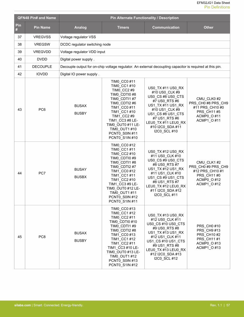
QFN48 Pin# and Name Pin Alternate Functionality / Description
Pin# Pin Name Analog Timers Communication Other
37 VREGVSS Voltage regulator VSS
38 VREGSW DCDC regulator switching node
39 VREGVDD Voltage regulator VDD input
40 DVDD Digital power supply .
41 DECOUPLE Decouple output for on-chip voltage regulator. An external decoupling capacitor is required at this pin.
42 IOVDD Digital IO power supply .
43 PC6BUSAX
BUSBY
TIM0_CC0 #11TIM0_CC1 #10TIM0_CC2 #9
TIM0_CDTI0 #8TIM0_CDTI1 #7TIM0_CDTI2 #6TIM1_CC0 #11TIM1_CC1 #10TIM1_CC2 #9
TIM1_CC3 #8 LE-TIM0_OUT0 #11 LE-
TIM0_OUT1 #10PCNT0_S0IN #11PCNT0_S1IN #10
US0_TX #11 US0_RX#10 US0_CLK #9
US0_CS #8 US0_CTS#7 US0_RTS #6
US1_TX #11 US1_RX#10 US1_CLK #9
US1_CS #8 US1_CTS#7 US1_RTS #6
LEU0_TX #11 LEU0_RX#10 I2C0_SDA #11
I2C0_SCL #10
CMU_CLK0 #2PRS_CH0 #8 PRS_CH9
#11 PRS_CH10 #0PRS_CH11 #5ACMP0_O #11ACMP1_O #11
44 PC7BUSAY
BUSBX
TIM0_CC0 #12TIM0_CC1 #11TIM0_CC2 #10TIM0_CDTI0 #9TIM0_CDTI1 #8TIM0_CDTI2 #7TIM1_CC0 #12TIM1_CC1 #11TIM1_CC2 #10
TIM1_CC3 #9 LE-TIM0_OUT0 #12 LE-
TIM0_OUT1 #11PCNT0_S0IN #12PCNT0_S1IN #11
US0_TX #12 US0_RX#11 US0_CLK #10
US0_CS #9 US0_CTS#8 US0_RTS #7
US1_TX #12 US1_RX#11 US1_CLK #10
US1_CS #9 US1_CTS#8 US1_RTS #7
LEU0_TX #12 LEU0_RX#11 I2C0_SDA #12
I2C0_SCL #11
CMU_CLK1 #2PRS_CH0 #9 PRS_CH9
#12 PRS_CH10 #1PRS_CH11 #0ACMP0_O #12ACMP1_O #12
45 PC8BUSAX
BUSBY
TIM0_CC0 #13TIM0_CC1 #12TIM0_CC2 #11
TIM0_CDTI0 #10TIM0_CDTI1 #9TIM0_CDTI2 #8TIM1_CC0 #13TIM1_CC1 #12TIM1_CC2 #11
TIM1_CC3 #10 LE-TIM0_OUT0 #13 LE-
TIM0_OUT1 #12PCNT0_S0IN #13PCNT0_S1IN #12
US0_TX #13 US0_RX#12 US0_CLK #11
US0_CS #10 US0_CTS#9 US0_RTS #8
US1_TX #13 US1_RX#12 US1_CLK #11
US1_CS #10 US1_CTS#9 US1_RTS #8
LEU0_TX #13 LEU0_RX#12 I2C0_SDA #13
I2C0_SCL #12
PRS_CH0 #10PRS_CH9 #13PRS_CH10 #2PRS_CH11 #1ACMP0_O #13ACMP1_O #13
EFM32JG1 Data SheetPin Definitions
silabs.com | Smart. Connected. Energy-friendly. Rev. 1.1 | 57
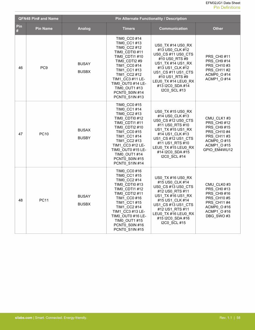
QFN48 Pin# and Name Pin Alternate Functionality / Description
Pin# Pin Name Analog Timers Communication Other
46 PC9BUSAY
BUSBX
TIM0_CC0 #14TIM0_CC1 #13TIM0_CC2 #12
TIM0_CDTI0 #11TIM0_CDTI1 #10TIM0_CDTI2 #9TIM1_CC0 #14TIM1_CC1 #13TIM1_CC2 #12
TIM1_CC3 #11 LE-TIM0_OUT0 #14 LE-
TIM0_OUT1 #13PCNT0_S0IN #14PCNT0_S1IN #13
US0_TX #14 US0_RX#13 US0_CLK #12
US0_CS #11 US0_CTS#10 US0_RTS #9
US1_TX #14 US1_RX#13 US1_CLK #12
US1_CS #11 US1_CTS#10 US1_RTS #9
LEU0_TX #14 LEU0_RX#13 I2C0_SDA #14
I2C0_SCL #13
PRS_CH0 #11PRS_CH9 #14PRS_CH10 #3PRS_CH11 #2ACMP0_O #14ACMP1_O #14
47 PC10BUSAX
BUSBY
TIM0_CC0 #15TIM0_CC1 #14TIM0_CC2 #13
TIM0_CDTI0 #12TIM0_CDTI1 #11TIM0_CDTI2 #10TIM1_CC0 #15TIM1_CC1 #14TIM1_CC2 #13
TIM1_CC3 #12 LE-TIM0_OUT0 #15 LE-
TIM0_OUT1 #14PCNT0_S0IN #15PCNT0_S1IN #14
US0_TX #15 US0_RX#14 US0_CLK #13
US0_CS #12 US0_CTS#11 US0_RTS #10
US1_TX #15 US1_RX#14 US1_CLK #13
US1_CS #12 US1_CTS#11 US1_RTS #10
LEU0_TX #15 LEU0_RX#14 I2C0_SDA #15
I2C0_SCL #14
CMU_CLK1 #3PRS_CH0 #12PRS_CH9 #15PRS_CH10 #4PRS_CH11 #3ACMP0_O #15ACMP1_O #15
GPIO_EM4WU12
48 PC11BUSAY
BUSBX
TIM0_CC0 #16TIM0_CC1 #15TIM0_CC2 #14
TIM0_CDTI0 #13TIM0_CDTI1 #12TIM0_CDTI2 #11TIM1_CC0 #16TIM1_CC1 #15TIM1_CC2 #14
TIM1_CC3 #13 LE-TIM0_OUT0 #16 LE-
TIM0_OUT1 #15PCNT0_S0IN #16PCNT0_S1IN #15
US0_TX #16 US0_RX#15 US0_CLK #14
US0_CS #13 US0_CTS#12 US0_RTS #11
US1_TX #16 US1_RX#15 US1_CLK #14
US1_CS #13 US1_CTS#12 US1_RTS #11
LEU0_TX #16 LEU0_RX#15 I2C0_SDA #16
I2C0_SCL #15
CMU_CLK0 #3PRS_CH0 #13PRS_CH9 #16PRS_CH10 #5PRS_CH11 #4ACMP0_O #16ACMP1_O #16DBG_SWO #3
EFM32JG1 Data SheetPin Definitions
silabs.com | Smart. Connected. Energy-friendly. Rev. 1.1 | 58

6.1.1 EFM32JG1 QFN48 with DC-DC GPIO Overview
The GPIO pins are organized as 16-bit ports indicated by letters (A, B, C...), and the individual pins on each port are indicated by anumber from 15 down to 0.
Table 6.2. QFN48 with DC-DC GPIO Pinout
Port Pin15
Pin14
Pin13
Pin12
Pin11
Pin10
Pin 9 Pin 8 Pin 7 Pin 6 Pin 5 Pin 4 Pin 3 Pin 2 Pin 1 Pin 0
Port A - - - - - - - - - - PA5(5V)
PA4(5V)
PA3(5V)
PA2(5V) PA1 PA0
Port B PB15 PB14 PB13(5V)
PB12(5V)
PB11(5V) - - - - - - - - - - -
Port C - - - - PC11(5V)
PC10(5V)
PC9(5V)
PC8(5V)
PC7(5V)
PC6(5V) - - - - - -
Port D PD15(5V)
PD14(5V)
PD13(5V)
PD12(5V)
PD11(5V)
PD10(5V)
PD9(5V) - - - - - - - - -
Port F - - - - - - - - PF7(5V)
PF6(5V)
PF5(5V)
PF4(5V)
PF3(5V)
PF2(5V)
PF1(5V)
PF0(5V)
Note:1. GPIO with 5V tolerance are indicated by (5V).2. The pins PA4, PA3, PA2, PB13, PB12, PB11, PD15, PD14, and PD13 will not be 5V tolerant on all future devices. In order to
preserve upgrade options with full hardware compatibility, do not use these pins with 5V domains.
EFM32JG1 Data SheetPin Definitions
silabs.com | Smart. Connected. Energy-friendly. Rev. 1.1 | 59
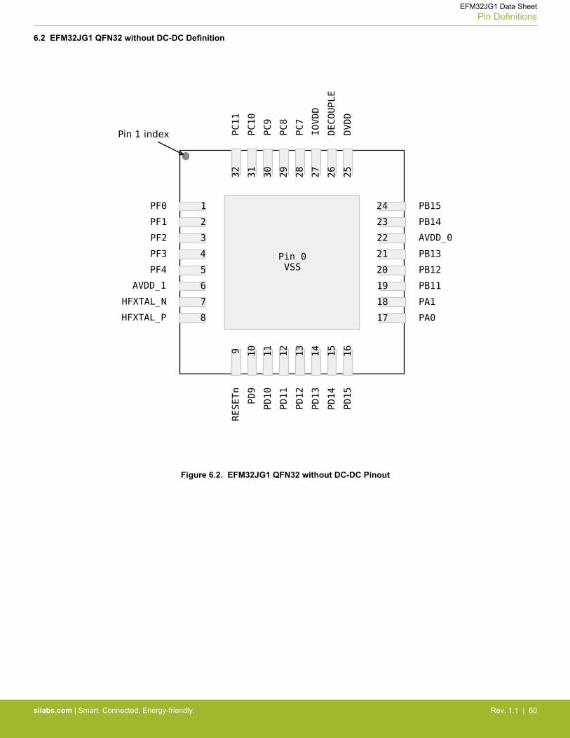
6.2 EFM32JG1 QFN32 without DC-DC Definition
Figure 6.2. EFM32JG1 QFN32 without DC-DC Pinout
EFM32JG1 Data SheetPin Definitions
silabs.com | Smart. Connected. Energy-friendly. Rev. 1.1 | 60

Table 6.3. QFN32 without DC-DC Device Pinout
QFN32 Pin# and Name Pin Alternate Functionality / Description
Pin# Pin Name Analog Timers Communication Other
0 VREGVSS Voltage regulator VSS
1 PF0BUSAX
BUSBY
TIM0_CC0 #24TIM0_CC1 #23TIM0_CC2 #22
TIM0_CDTI0 #21TIM0_CDTI1 #20TIM0_CDTI2 #19TIM1_CC0 #24TIM1_CC1 #23TIM1_CC2 #22
TIM1_CC3 #21 LE-TIM0_OUT0 #24 LE-
TIM0_OUT1 #23PCNT0_S0IN #24PCNT0_S1IN #23
US0_TX #24 US0_RX#23 US0_CLK #22
US0_CS #21 US0_CTS#20 US0_RTS #19
US1_TX #24 US1_RX#23 US1_CLK #22
US1_CS #21 US1_CTS#20 US1_RTS #19
LEU0_TX #24 LEU0_RX#23 I2C0_SDA #24
I2C0_SCL #23
PRS_CH0 #0 PRS_CH1#7 PRS_CH2 #6
PRS_CH3 #5 ACMP0_O#24 ACMP1_O #24
DBG_SWCLKTCK #0BOOT_TX
2 PF1BUSAY
BUSBX
TIM0_CC0 #25TIM0_CC1 #24TIM0_CC2 #23
TIM0_CDTI0 #22TIM0_CDTI1 #21TIM0_CDTI2 #20TIM1_CC0 #25TIM1_CC1 #24TIM1_CC2 #23
TIM1_CC3 #22 LE-TIM0_OUT0 #25 LE-
TIM0_OUT1 #24PCNT0_S0IN #25PCNT0_S1IN #24
US0_TX #25 US0_RX#24 US0_CLK #23
US0_CS #22 US0_CTS#21 US0_RTS #20
US1_TX #25 US1_RX#24 US1_CLK #23
US1_CS #22 US1_CTS#21 US1_RTS #20
LEU0_TX #25 LEU0_RX#24 I2C0_SDA #25
I2C0_SCL #24
PRS_CH0 #1 PRS_CH1#0 PRS_CH2 #7
PRS_CH3 #6 ACMP0_O#25 ACMP1_O #25
DBG_SWDIOTMS #0BOOT_RX
3 PF2BUSAX
BUSBY
TIM0_CC0 #26TIM0_CC1 #25TIM0_CC2 #24
TIM0_CDTI0 #23TIM0_CDTI1 #22TIM0_CDTI2 #21TIM1_CC0 #26TIM1_CC1 #25TIM1_CC2 #24
TIM1_CC3 #23 LE-TIM0_OUT0 #26 LE-
TIM0_OUT1 #25PCNT0_S0IN #26PCNT0_S1IN #25
US0_TX #26 US0_RX#25 US0_CLK #24
US0_CS #23 US0_CTS#22 US0_RTS #21
US1_TX #26 US1_RX#25 US1_CLK #24
US1_CS #23 US1_CTS#22 US1_RTS #21
LEU0_TX #26 LEU0_RX#25 I2C0_SDA #26
I2C0_SCL #25
CMU_CLK0 #6PRS_CH0 #2 PRS_CH1
#1 PRS_CH2 #0PRS_CH3 #7 ACMP0_O
#26 ACMP1_O #26DBG_TDO #0DBG_SWO #0
GPIO_EM4WU0
EFM32JG1 Data SheetPin Definitions
silabs.com | Smart. Connected. Energy-friendly. Rev. 1.1 | 61
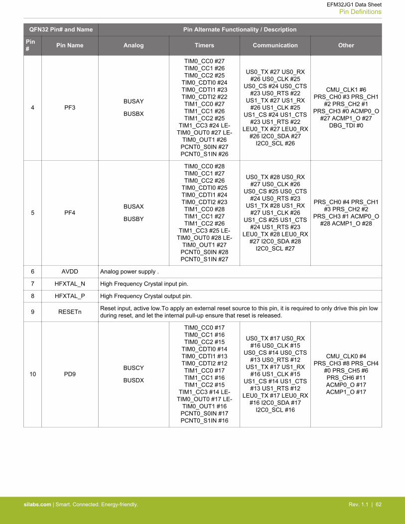
QFN32 Pin# and Name Pin Alternate Functionality / Description
Pin# Pin Name Analog Timers Communication Other
4 PF3BUSAY
BUSBX
TIM0_CC0 #27TIM0_CC1 #26TIM0_CC2 #25
TIM0_CDTI0 #24TIM0_CDTI1 #23TIM0_CDTI2 #22TIM1_CC0 #27TIM1_CC1 #26TIM1_CC2 #25
TIM1_CC3 #24 LE-TIM0_OUT0 #27 LE-
TIM0_OUT1 #26PCNT0_S0IN #27PCNT0_S1IN #26
US0_TX #27 US0_RX#26 US0_CLK #25
US0_CS #24 US0_CTS#23 US0_RTS #22
US1_TX #27 US1_RX#26 US1_CLK #25
US1_CS #24 US1_CTS#23 US1_RTS #22
LEU0_TX #27 LEU0_RX#26 I2C0_SDA #27
I2C0_SCL #26
CMU_CLK1 #6PRS_CH0 #3 PRS_CH1
#2 PRS_CH2 #1PRS_CH3 #0 ACMP0_O
#27 ACMP1_O #27DBG_TDI #0
5 PF4BUSAX
BUSBY
TIM0_CC0 #28TIM0_CC1 #27TIM0_CC2 #26
TIM0_CDTI0 #25TIM0_CDTI1 #24TIM0_CDTI2 #23TIM1_CC0 #28TIM1_CC1 #27TIM1_CC2 #26
TIM1_CC3 #25 LE-TIM0_OUT0 #28 LE-
TIM0_OUT1 #27PCNT0_S0IN #28PCNT0_S1IN #27
US0_TX #28 US0_RX#27 US0_CLK #26
US0_CS #25 US0_CTS#24 US0_RTS #23
US1_TX #28 US1_RX#27 US1_CLK #26
US1_CS #25 US1_CTS#24 US1_RTS #23
LEU0_TX #28 LEU0_RX#27 I2C0_SDA #28
I2C0_SCL #27
PRS_CH0 #4 PRS_CH1#3 PRS_CH2 #2
PRS_CH3 #1 ACMP0_O#28 ACMP1_O #28
6 AVDD Analog power supply .
7 HFXTAL_N High Frequency Crystal input pin.
8 HFXTAL_P High Frequency Crystal output pin.
9 RESETn Reset input, active low.To apply an external reset source to this pin, it is required to only drive this pin lowduring reset, and let the internal pull-up ensure that reset is released.
10 PD9BUSCY
BUSDX
TIM0_CC0 #17TIM0_CC1 #16TIM0_CC2 #15
TIM0_CDTI0 #14TIM0_CDTI1 #13TIM0_CDTI2 #12TIM1_CC0 #17TIM1_CC1 #16TIM1_CC2 #15
TIM1_CC3 #14 LE-TIM0_OUT0 #17 LE-
TIM0_OUT1 #16PCNT0_S0IN #17PCNT0_S1IN #16
US0_TX #17 US0_RX#16 US0_CLK #15
US0_CS #14 US0_CTS#13 US0_RTS #12
US1_TX #17 US1_RX#16 US1_CLK #15
US1_CS #14 US1_CTS#13 US1_RTS #12
LEU0_TX #17 LEU0_RX#16 I2C0_SDA #17
I2C0_SCL #16
CMU_CLK0 #4PRS_CH3 #8 PRS_CH4
#0 PRS_CH5 #6PRS_CH6 #11ACMP0_O #17ACMP1_O #17
EFM32JG1 Data SheetPin Definitions
silabs.com | Smart. Connected. Energy-friendly. Rev. 1.1 | 62

QFN32 Pin# and Name Pin Alternate Functionality / Description
Pin# Pin Name Analog Timers Communication Other
11 PD10BUSCX
BUSDY
TIM0_CC0 #18TIM0_CC1 #17TIM0_CC2 #16
TIM0_CDTI0 #15TIM0_CDTI1 #14TIM0_CDTI2 #13TIM1_CC0 #18TIM1_CC1 #17TIM1_CC2 #16
TIM1_CC3 #15 LE-TIM0_OUT0 #18 LE-
TIM0_OUT1 #17PCNT0_S0IN #18PCNT0_S1IN #17
US0_TX #18 US0_RX#17 US0_CLK #16
US0_CS #15 US0_CTS#14 US0_RTS #13
US1_TX #18 US1_RX#17 US1_CLK #16
US1_CS #15 US1_CTS#14 US1_RTS #13
LEU0_TX #18 LEU0_RX#17 I2C0_SDA #18
I2C0_SCL #17
CMU_CLK1 #4PRS_CH3 #9 PRS_CH4
#1 PRS_CH5 #0PRS_CH6 #12ACMP0_O #18ACMP1_O #18
12 PD11BUSCY
BUSDX
TIM0_CC0 #19TIM0_CC1 #18TIM0_CC2 #17
TIM0_CDTI0 #16TIM0_CDTI1 #15TIM0_CDTI2 #14TIM1_CC0 #19TIM1_CC1 #18TIM1_CC2 #17
TIM1_CC3 #16 LE-TIM0_OUT0 #19 LE-
TIM0_OUT1 #18PCNT0_S0IN #19PCNT0_S1IN #18
US0_TX #19 US0_RX#18 US0_CLK #17
US0_CS #16 US0_CTS#15 US0_RTS #14
US1_TX #19 US1_RX#18 US1_CLK #17
US1_CS #16 US1_CTS#15 US1_RTS #14
LEU0_TX #19 LEU0_RX#18 I2C0_SDA #19
I2C0_SCL #18
PRS_CH3 #10PRS_CH4 #2 PRS_CH5
#1 PRS_CH6 #13ACMP0_O #19ACMP1_O #19
13 PD12BUSCX
BUSDY
TIM0_CC0 #20TIM0_CC1 #19TIM0_CC2 #18
TIM0_CDTI0 #17TIM0_CDTI1 #16TIM0_CDTI2 #15TIM1_CC0 #20TIM1_CC1 #19TIM1_CC2 #18
TIM1_CC3 #17 LE-TIM0_OUT0 #20 LE-
TIM0_OUT1 #19PCNT0_S0IN #20PCNT0_S1IN #19
US0_TX #20 US0_RX#19 US0_CLK #18
US0_CS #17 US0_CTS#16 US0_RTS #15
US1_TX #20 US1_RX#19 US1_CLK #18
US1_CS #17 US1_CTS#16 US1_RTS #15
LEU0_TX #20 LEU0_RX#19 I2C0_SDA #20
I2C0_SCL #19
PRS_CH3 #11PRS_CH4 #3 PRS_CH5
#2 PRS_CH6 #14ACMP0_O #20ACMP1_O #20
14 PD13BUSCY
BUSDX
TIM0_CC0 #21TIM0_CC1 #20TIM0_CC2 #19
TIM0_CDTI0 #18TIM0_CDTI1 #17TIM0_CDTI2 #16TIM1_CC0 #21TIM1_CC1 #20TIM1_CC2 #19
TIM1_CC3 #18 LE-TIM0_OUT0 #21 LE-
TIM0_OUT1 #20PCNT0_S0IN #21PCNT0_S1IN #20
US0_TX #21 US0_RX#20 US0_CLK #19
US0_CS #18 US0_CTS#17 US0_RTS #16
US1_TX #21 US1_RX#20 US1_CLK #19
US1_CS #18 US1_CTS#17 US1_RTS #16
LEU0_TX #21 LEU0_RX#20 I2C0_SDA #21
I2C0_SCL #20
PRS_CH3 #12PRS_CH4 #4 PRS_CH5
#3 PRS_CH6 #15ACMP0_O #21ACMP1_O #21
EFM32JG1 Data SheetPin Definitions
silabs.com | Smart. Connected. Energy-friendly. Rev. 1.1 | 63
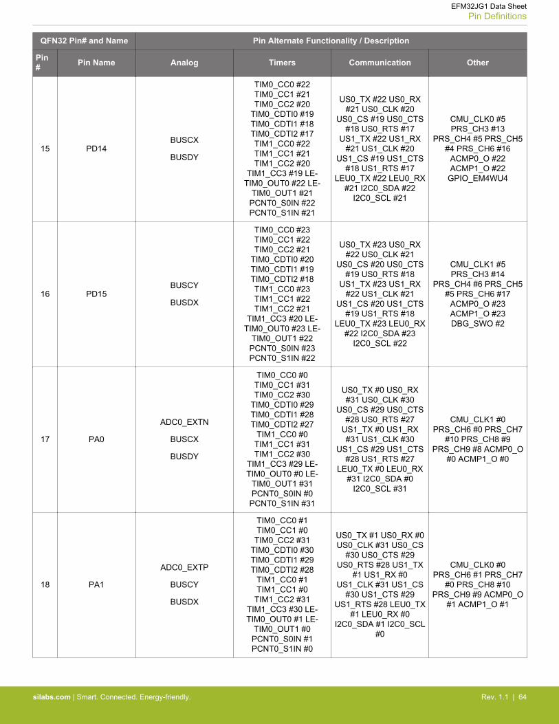
QFN32 Pin# and Name Pin Alternate Functionality / Description
Pin# Pin Name Analog Timers Communication Other
15 PD14BUSCX
BUSDY
TIM0_CC0 #22TIM0_CC1 #21TIM0_CC2 #20
TIM0_CDTI0 #19TIM0_CDTI1 #18TIM0_CDTI2 #17TIM1_CC0 #22TIM1_CC1 #21TIM1_CC2 #20
TIM1_CC3 #19 LE-TIM0_OUT0 #22 LE-
TIM0_OUT1 #21PCNT0_S0IN #22PCNT0_S1IN #21
US0_TX #22 US0_RX#21 US0_CLK #20
US0_CS #19 US0_CTS#18 US0_RTS #17
US1_TX #22 US1_RX#21 US1_CLK #20
US1_CS #19 US1_CTS#18 US1_RTS #17
LEU0_TX #22 LEU0_RX#21 I2C0_SDA #22
I2C0_SCL #21
CMU_CLK0 #5PRS_CH3 #13
PRS_CH4 #5 PRS_CH5#4 PRS_CH6 #16
ACMP0_O #22ACMP1_O #22
GPIO_EM4WU4
16 PD15BUSCY
BUSDX
TIM0_CC0 #23TIM0_CC1 #22TIM0_CC2 #21
TIM0_CDTI0 #20TIM0_CDTI1 #19TIM0_CDTI2 #18TIM1_CC0 #23TIM1_CC1 #22TIM1_CC2 #21
TIM1_CC3 #20 LE-TIM0_OUT0 #23 LE-
TIM0_OUT1 #22PCNT0_S0IN #23PCNT0_S1IN #22
US0_TX #23 US0_RX#22 US0_CLK #21
US0_CS #20 US0_CTS#19 US0_RTS #18
US1_TX #23 US1_RX#22 US1_CLK #21
US1_CS #20 US1_CTS#19 US1_RTS #18
LEU0_TX #23 LEU0_RX#22 I2C0_SDA #23
I2C0_SCL #22
CMU_CLK1 #5PRS_CH3 #14
PRS_CH4 #6 PRS_CH5#5 PRS_CH6 #17
ACMP0_O #23ACMP1_O #23DBG_SWO #2
17 PA0
ADC0_EXTN
BUSCX
BUSDY
TIM0_CC0 #0TIM0_CC1 #31TIM0_CC2 #30
TIM0_CDTI0 #29TIM0_CDTI1 #28TIM0_CDTI2 #27
TIM1_CC0 #0TIM1_CC1 #31TIM1_CC2 #30
TIM1_CC3 #29 LE-TIM0_OUT0 #0 LE-
TIM0_OUT1 #31PCNT0_S0IN #0
PCNT0_S1IN #31
US0_TX #0 US0_RX#31 US0_CLK #30
US0_CS #29 US0_CTS#28 US0_RTS #27
US1_TX #0 US1_RX#31 US1_CLK #30
US1_CS #29 US1_CTS#28 US1_RTS #27
LEU0_TX #0 LEU0_RX#31 I2C0_SDA #0
I2C0_SCL #31
CMU_CLK1 #0PRS_CH6 #0 PRS_CH7
#10 PRS_CH8 #9PRS_CH9 #8 ACMP0_O
#0 ACMP1_O #0
18 PA1
ADC0_EXTP
BUSCY
BUSDX
TIM0_CC0 #1TIM0_CC1 #0
TIM0_CC2 #31TIM0_CDTI0 #30TIM0_CDTI1 #29TIM0_CDTI2 #28
TIM1_CC0 #1TIM1_CC1 #0
TIM1_CC2 #31TIM1_CC3 #30 LE-TIM0_OUT0 #1 LE-
TIM0_OUT1 #0PCNT0_S0IN #1PCNT0_S1IN #0
US0_TX #1 US0_RX #0US0_CLK #31 US0_CS
#30 US0_CTS #29US0_RTS #28 US1_TX
#1 US1_RX #0US1_CLK #31 US1_CS
#30 US1_CTS #29US1_RTS #28 LEU0_TX
#1 LEU0_RX #0I2C0_SDA #1 I2C0_SCL
#0
CMU_CLK0 #0PRS_CH6 #1 PRS_CH7
#0 PRS_CH8 #10PRS_CH9 #9 ACMP0_O
#1 ACMP1_O #1
EFM32JG1 Data SheetPin Definitions
silabs.com | Smart. Connected. Energy-friendly. Rev. 1.1 | 64
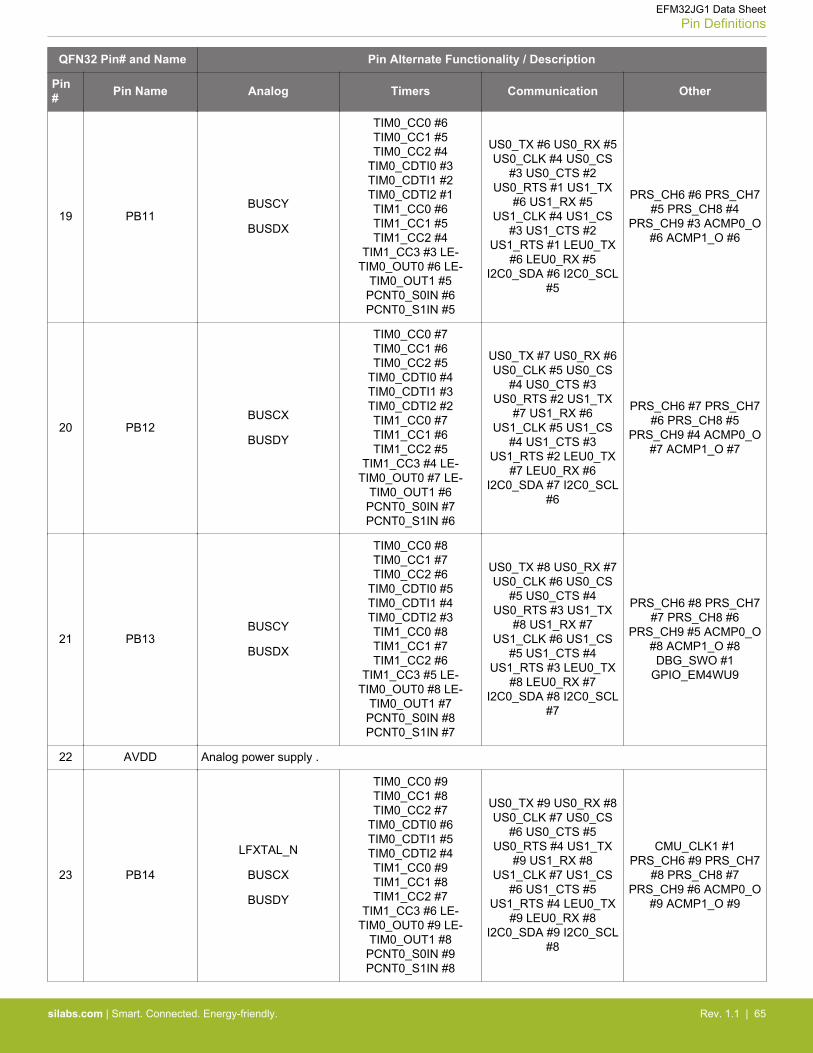
QFN32 Pin# and Name Pin Alternate Functionality / Description
Pin# Pin Name Analog Timers Communication Other
19 PB11BUSCY
BUSDX
TIM0_CC0 #6TIM0_CC1 #5TIM0_CC2 #4
TIM0_CDTI0 #3TIM0_CDTI1 #2TIM0_CDTI2 #1TIM1_CC0 #6TIM1_CC1 #5TIM1_CC2 #4
TIM1_CC3 #3 LE-TIM0_OUT0 #6 LE-
TIM0_OUT1 #5PCNT0_S0IN #6PCNT0_S1IN #5
US0_TX #6 US0_RX #5US0_CLK #4 US0_CS
#3 US0_CTS #2US0_RTS #1 US1_TX
#6 US1_RX #5US1_CLK #4 US1_CS
#3 US1_CTS #2US1_RTS #1 LEU0_TX
#6 LEU0_RX #5I2C0_SDA #6 I2C0_SCL
#5
PRS_CH6 #6 PRS_CH7#5 PRS_CH8 #4
PRS_CH9 #3 ACMP0_O#6 ACMP1_O #6
20 PB12BUSCX
BUSDY
TIM0_CC0 #7TIM0_CC1 #6TIM0_CC2 #5
TIM0_CDTI0 #4TIM0_CDTI1 #3TIM0_CDTI2 #2TIM1_CC0 #7TIM1_CC1 #6TIM1_CC2 #5
TIM1_CC3 #4 LE-TIM0_OUT0 #7 LE-
TIM0_OUT1 #6PCNT0_S0IN #7PCNT0_S1IN #6
US0_TX #7 US0_RX #6US0_CLK #5 US0_CS
#4 US0_CTS #3US0_RTS #2 US1_TX
#7 US1_RX #6US1_CLK #5 US1_CS
#4 US1_CTS #3US1_RTS #2 LEU0_TX
#7 LEU0_RX #6I2C0_SDA #7 I2C0_SCL
#6
PRS_CH6 #7 PRS_CH7#6 PRS_CH8 #5
PRS_CH9 #4 ACMP0_O#7 ACMP1_O #7
21 PB13BUSCY
BUSDX
TIM0_CC0 #8TIM0_CC1 #7TIM0_CC2 #6
TIM0_CDTI0 #5TIM0_CDTI1 #4TIM0_CDTI2 #3TIM1_CC0 #8TIM1_CC1 #7TIM1_CC2 #6
TIM1_CC3 #5 LE-TIM0_OUT0 #8 LE-
TIM0_OUT1 #7PCNT0_S0IN #8PCNT0_S1IN #7
US0_TX #8 US0_RX #7US0_CLK #6 US0_CS
#5 US0_CTS #4US0_RTS #3 US1_TX
#8 US1_RX #7US1_CLK #6 US1_CS
#5 US1_CTS #4US1_RTS #3 LEU0_TX
#8 LEU0_RX #7I2C0_SDA #8 I2C0_SCL
#7
PRS_CH6 #8 PRS_CH7#7 PRS_CH8 #6
PRS_CH9 #5 ACMP0_O#8 ACMP1_O #8DBG_SWO #1
GPIO_EM4WU9
22 AVDD Analog power supply .
23 PB14
LFXTAL_N
BUSCX
BUSDY
TIM0_CC0 #9TIM0_CC1 #8TIM0_CC2 #7
TIM0_CDTI0 #6TIM0_CDTI1 #5TIM0_CDTI2 #4TIM1_CC0 #9TIM1_CC1 #8TIM1_CC2 #7
TIM1_CC3 #6 LE-TIM0_OUT0 #9 LE-
TIM0_OUT1 #8PCNT0_S0IN #9PCNT0_S1IN #8
US0_TX #9 US0_RX #8US0_CLK #7 US0_CS
#6 US0_CTS #5US0_RTS #4 US1_TX
#9 US1_RX #8US1_CLK #7 US1_CS
#6 US1_CTS #5US1_RTS #4 LEU0_TX
#9 LEU0_RX #8I2C0_SDA #9 I2C0_SCL
#8
CMU_CLK1 #1PRS_CH6 #9 PRS_CH7
#8 PRS_CH8 #7PRS_CH9 #6 ACMP0_O
#9 ACMP1_O #9
EFM32JG1 Data SheetPin Definitions
silabs.com | Smart. Connected. Energy-friendly. Rev. 1.1 | 65
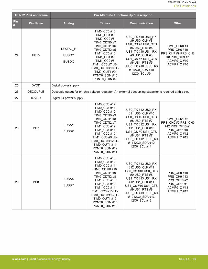
QFN32 Pin# and Name Pin Alternate Functionality / Description
Pin# Pin Name Analog Timers Communication Other
24 PB15
LFXTAL_P
BUSCY
BUSDX
TIM0_CC0 #10TIM0_CC1 #9TIM0_CC2 #8
TIM0_CDTI0 #7TIM0_CDTI1 #6TIM0_CDTI2 #5TIM1_CC0 #10TIM1_CC1 #9TIM1_CC2 #8
TIM1_CC3 #7 LE-TIM0_OUT0 #10 LE-
TIM0_OUT1 #9PCNT0_S0IN #10PCNT0_S1IN #9
US0_TX #10 US0_RX#9 US0_CLK #8
US0_CS #7 US0_CTS#6 US0_RTS #5
US1_TX #10 US1_RX#9 US1_CLK #8
US1_CS #7 US1_CTS#6 US1_RTS #5
LEU0_TX #10 LEU0_RX#9 I2C0_SDA #10
I2C0_SCL #9
CMU_CLK0 #1PRS_CH6 #10
PRS_CH7 #9 PRS_CH8#8 PRS_CH9 #7ACMP0_O #10ACMP1_O #10
25 DVDD Digital power supply .
26 DECOUPLE Decouple output for on-chip voltage regulator. An external decoupling capacitor is required at this pin.
27 IOVDD Digital IO power supply .
28 PC7BUSAY
BUSBX
TIM0_CC0 #12TIM0_CC1 #11TIM0_CC2 #10TIM0_CDTI0 #9TIM0_CDTI1 #8TIM0_CDTI2 #7TIM1_CC0 #12TIM1_CC1 #11TIM1_CC2 #10
TIM1_CC3 #9 LE-TIM0_OUT0 #12 LE-
TIM0_OUT1 #11PCNT0_S0IN #12PCNT0_S1IN #11
US0_TX #12 US0_RX#11 US0_CLK #10
US0_CS #9 US0_CTS#8 US0_RTS #7
US1_TX #12 US1_RX#11 US1_CLK #10
US1_CS #9 US1_CTS#8 US1_RTS #7
LEU0_TX #12 LEU0_RX#11 I2C0_SDA #12
I2C0_SCL #11
CMU_CLK1 #2PRS_CH0 #9 PRS_CH9
#12 PRS_CH10 #1PRS_CH11 #0ACMP0_O #12ACMP1_O #12
29 PC8BUSAX
BUSBY
TIM0_CC0 #13TIM0_CC1 #12TIM0_CC2 #11
TIM0_CDTI0 #10TIM0_CDTI1 #9TIM0_CDTI2 #8TIM1_CC0 #13TIM1_CC1 #12TIM1_CC2 #11
TIM1_CC3 #10 LE-TIM0_OUT0 #13 LE-
TIM0_OUT1 #12PCNT0_S0IN #13PCNT0_S1IN #12
US0_TX #13 US0_RX#12 US0_CLK #11
US0_CS #10 US0_CTS#9 US0_RTS #8
US1_TX #13 US1_RX#12 US1_CLK #11
US1_CS #10 US1_CTS#9 US1_RTS #8
LEU0_TX #13 LEU0_RX#12 I2C0_SDA #13
I2C0_SCL #12
PRS_CH0 #10PRS_CH9 #13PRS_CH10 #2PRS_CH11 #1ACMP0_O #13ACMP1_O #13
EFM32JG1 Data SheetPin Definitions
silabs.com | Smart. Connected. Energy-friendly. Rev. 1.1 | 66

QFN32 Pin# and Name Pin Alternate Functionality / Description
Pin# Pin Name Analog Timers Communication Other
30 PC9BUSAY
BUSBX
TIM0_CC0 #14TIM0_CC1 #13TIM0_CC2 #12
TIM0_CDTI0 #11TIM0_CDTI1 #10TIM0_CDTI2 #9TIM1_CC0 #14TIM1_CC1 #13TIM1_CC2 #12
TIM1_CC3 #11 LE-TIM0_OUT0 #14 LE-
TIM0_OUT1 #13PCNT0_S0IN #14PCNT0_S1IN #13
US0_TX #14 US0_RX#13 US0_CLK #12
US0_CS #11 US0_CTS#10 US0_RTS #9
US1_TX #14 US1_RX#13 US1_CLK #12
US1_CS #11 US1_CTS#10 US1_RTS #9
LEU0_TX #14 LEU0_RX#13 I2C0_SDA #14
I2C0_SCL #13
PRS_CH0 #11PRS_CH9 #14PRS_CH10 #3PRS_CH11 #2ACMP0_O #14ACMP1_O #14
31 PC10BUSAX
BUSBY
TIM0_CC0 #15TIM0_CC1 #14TIM0_CC2 #13
TIM0_CDTI0 #12TIM0_CDTI1 #11TIM0_CDTI2 #10TIM1_CC0 #15TIM1_CC1 #14TIM1_CC2 #13
TIM1_CC3 #12 LE-TIM0_OUT0 #15 LE-
TIM0_OUT1 #14PCNT0_S0IN #15PCNT0_S1IN #14
US0_TX #15 US0_RX#14 US0_CLK #13
US0_CS #12 US0_CTS#11 US0_RTS #10
US1_TX #15 US1_RX#14 US1_CLK #13
US1_CS #12 US1_CTS#11 US1_RTS #10
LEU0_TX #15 LEU0_RX#14 I2C0_SDA #15
I2C0_SCL #14
CMU_CLK1 #3PRS_CH0 #12PRS_CH9 #15PRS_CH10 #4PRS_CH11 #3ACMP0_O #15ACMP1_O #15
GPIO_EM4WU12
32 PC11BUSAY
BUSBX
TIM0_CC0 #16TIM0_CC1 #15TIM0_CC2 #14
TIM0_CDTI0 #13TIM0_CDTI1 #12TIM0_CDTI2 #11TIM1_CC0 #16TIM1_CC1 #15TIM1_CC2 #14
TIM1_CC3 #13 LE-TIM0_OUT0 #16 LE-
TIM0_OUT1 #15PCNT0_S0IN #16PCNT0_S1IN #15
US0_TX #16 US0_RX#15 US0_CLK #14
US0_CS #13 US0_CTS#12 US0_RTS #11
US1_TX #16 US1_RX#15 US1_CLK #14
US1_CS #13 US1_CTS#12 US1_RTS #11
LEU0_TX #16 LEU0_RX#15 I2C0_SDA #16
I2C0_SCL #15
CMU_CLK0 #3PRS_CH0 #13PRS_CH9 #16PRS_CH10 #5PRS_CH11 #4ACMP0_O #16ACMP1_O #16DBG_SWO #3
EFM32JG1 Data SheetPin Definitions
silabs.com | Smart. Connected. Energy-friendly. Rev. 1.1 | 67
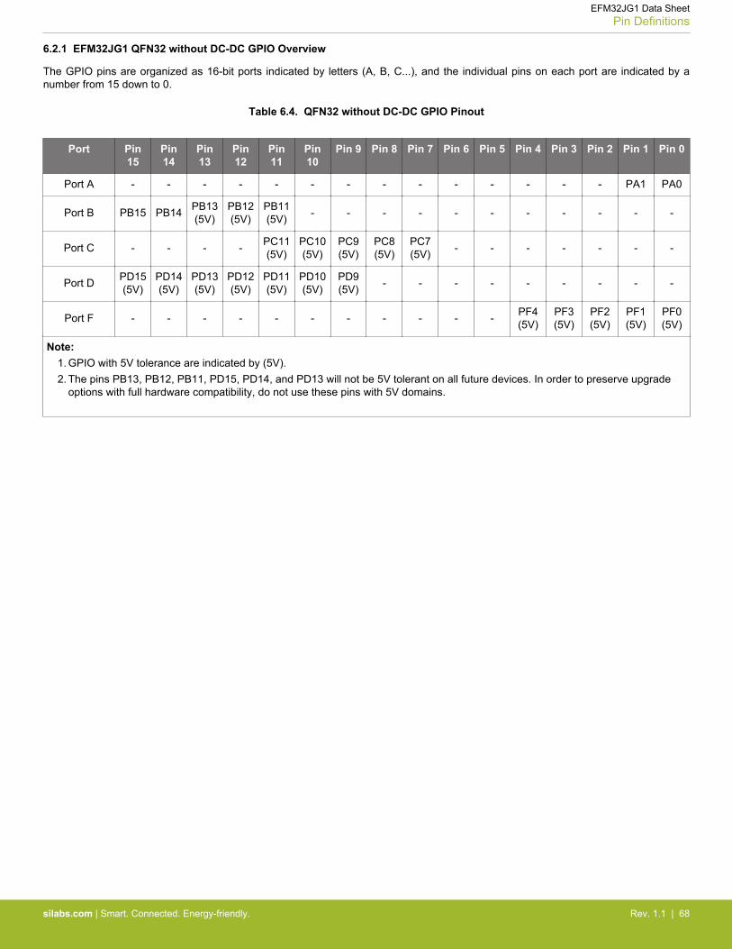
6.2.1 EFM32JG1 QFN32 without DC-DC GPIO Overview
The GPIO pins are organized as 16-bit ports indicated by letters (A, B, C...), and the individual pins on each port are indicated by anumber from 15 down to 0.
Table 6.4. QFN32 without DC-DC GPIO Pinout
Port Pin15
Pin14
Pin13
Pin12
Pin11
Pin10
Pin 9 Pin 8 Pin 7 Pin 6 Pin 5 Pin 4 Pin 3 Pin 2 Pin 1 Pin 0
Port A - - - - - - - - - - - - - - PA1 PA0
Port B PB15 PB14 PB13(5V)
PB12(5V)
PB11(5V) - - - - - - - - - - -
Port C - - - - PC11(5V)
PC10(5V)
PC9(5V)
PC8(5V)
PC7(5V) - - - - - - -
Port D PD15(5V)
PD14(5V)
PD13(5V)
PD12(5V)
PD11(5V)
PD10(5V)
PD9(5V) - - - - - - - - -
Port F - - - - - - - - - - - PF4(5V)
PF3(5V)
PF2(5V)
PF1(5V)
PF0(5V)
Note:1. GPIO with 5V tolerance are indicated by (5V).2. The pins PB13, PB12, PB11, PD15, PD14, and PD13 will not be 5V tolerant on all future devices. In order to preserve upgrade
options with full hardware compatibility, do not use these pins with 5V domains.
EFM32JG1 Data SheetPin Definitions
silabs.com | Smart. Connected. Energy-friendly. Rev. 1.1 | 68
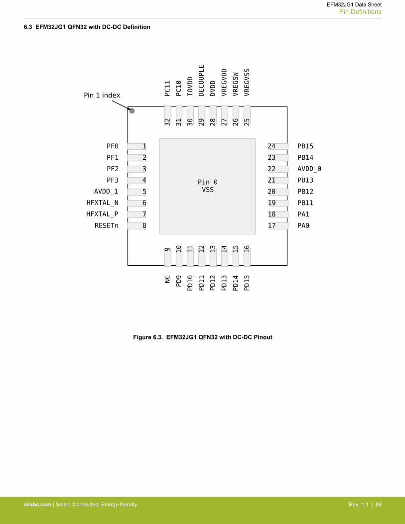
6.3 EFM32JG1 QFN32 with DC-DC Definition
Figure 6.3. EFM32JG1 QFN32 with DC-DC Pinout
EFM32JG1 Data SheetPin Definitions
silabs.com | Smart. Connected. Energy-friendly. Rev. 1.1 | 69
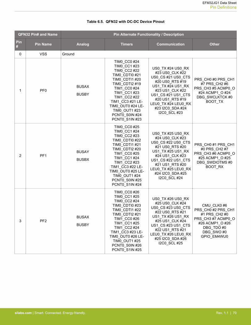
Table 6.5. QFN32 with DC-DC Device Pinout
QFN32 Pin# and Name Pin Alternate Functionality / Description
Pin# Pin Name Analog Timers Communication Other
0 VSS Ground
1 PF0BUSAX
BUSBY
TIM0_CC0 #24TIM0_CC1 #23TIM0_CC2 #22
TIM0_CDTI0 #21TIM0_CDTI1 #20TIM0_CDTI2 #19TIM1_CC0 #24TIM1_CC1 #23TIM1_CC2 #22
TIM1_CC3 #21 LE-TIM0_OUT0 #24 LE-
TIM0_OUT1 #23PCNT0_S0IN #24PCNT0_S1IN #23
US0_TX #24 US0_RX#23 US0_CLK #22
US0_CS #21 US0_CTS#20 US0_RTS #19
US1_TX #24 US1_RX#23 US1_CLK #22
US1_CS #21 US1_CTS#20 US1_RTS #19
LEU0_TX #24 LEU0_RX#23 I2C0_SDA #24
I2C0_SCL #23
PRS_CH0 #0 PRS_CH1#7 PRS_CH2 #6
PRS_CH3 #5 ACMP0_O#24 ACMP1_O #24
DBG_SWCLKTCK #0BOOT_TX
2 PF1BUSAY
BUSBX
TIM0_CC0 #25TIM0_CC1 #24TIM0_CC2 #23
TIM0_CDTI0 #22TIM0_CDTI1 #21TIM0_CDTI2 #20TIM1_CC0 #25TIM1_CC1 #24TIM1_CC2 #23
TIM1_CC3 #22 LE-TIM0_OUT0 #25 LE-
TIM0_OUT1 #24PCNT0_S0IN #25PCNT0_S1IN #24
US0_TX #25 US0_RX#24 US0_CLK #23
US0_CS #22 US0_CTS#21 US0_RTS #20
US1_TX #25 US1_RX#24 US1_CLK #23
US1_CS #22 US1_CTS#21 US1_RTS #20
LEU0_TX #25 LEU0_RX#24 I2C0_SDA #25
I2C0_SCL #24
PRS_CH0 #1 PRS_CH1#0 PRS_CH2 #7
PRS_CH3 #6 ACMP0_O#25 ACMP1_O #25
DBG_SWDIOTMS #0BOOT_RX
3 PF2BUSAX
BUSBY
TIM0_CC0 #26TIM0_CC1 #25TIM0_CC2 #24
TIM0_CDTI0 #23TIM0_CDTI1 #22TIM0_CDTI2 #21TIM1_CC0 #26TIM1_CC1 #25TIM1_CC2 #24
TIM1_CC3 #23 LE-TIM0_OUT0 #26 LE-
TIM0_OUT1 #25PCNT0_S0IN #26PCNT0_S1IN #25
US0_TX #26 US0_RX#25 US0_CLK #24
US0_CS #23 US0_CTS#22 US0_RTS #21
US1_TX #26 US1_RX#25 US1_CLK #24
US1_CS #23 US1_CTS#22 US1_RTS #21
LEU0_TX #26 LEU0_RX#25 I2C0_SDA #26
I2C0_SCL #25
CMU_CLK0 #6PRS_CH0 #2 PRS_CH1
#1 PRS_CH2 #0PRS_CH3 #7 ACMP0_O
#26 ACMP1_O #26DBG_TDO #0DBG_SWO #0
GPIO_EM4WU0
EFM32JG1 Data SheetPin Definitions
silabs.com | Smart. Connected. Energy-friendly. Rev. 1.1 | 70

QFN32 Pin# and Name Pin Alternate Functionality / Description
Pin# Pin Name Analog Timers Communication Other
4 PF3BUSAY
BUSBX
TIM0_CC0 #27TIM0_CC1 #26TIM0_CC2 #25
TIM0_CDTI0 #24TIM0_CDTI1 #23TIM0_CDTI2 #22TIM1_CC0 #27TIM1_CC1 #26TIM1_CC2 #25
TIM1_CC3 #24 LE-TIM0_OUT0 #27 LE-
TIM0_OUT1 #26PCNT0_S0IN #27PCNT0_S1IN #26
US0_TX #27 US0_RX#26 US0_CLK #25
US0_CS #24 US0_CTS#23 US0_RTS #22
US1_TX #27 US1_RX#26 US1_CLK #25
US1_CS #24 US1_CTS#23 US1_RTS #22
LEU0_TX #27 LEU0_RX#26 I2C0_SDA #27
I2C0_SCL #26
CMU_CLK1 #6PRS_CH0 #3 PRS_CH1
#2 PRS_CH2 #1PRS_CH3 #0 ACMP0_O
#27 ACMP1_O #27DBG_TDI #0
5 AVDD Analog power supply .
6 HFXTAL_N High Frequency Crystal input pin.
7 HFXTAL_P High Frequency Crystal output pin.
8 RESETn Reset input, active low.To apply an external reset source to this pin, it is required to only drive this pin lowduring reset, and let the internal pull-up ensure that reset is released.
9 NC No Connect.
10 PD9BUSCY
BUSDX
TIM0_CC0 #17TIM0_CC1 #16TIM0_CC2 #15
TIM0_CDTI0 #14TIM0_CDTI1 #13TIM0_CDTI2 #12TIM1_CC0 #17TIM1_CC1 #16TIM1_CC2 #15
TIM1_CC3 #14 LE-TIM0_OUT0 #17 LE-
TIM0_OUT1 #16PCNT0_S0IN #17PCNT0_S1IN #16
US0_TX #17 US0_RX#16 US0_CLK #15
US0_CS #14 US0_CTS#13 US0_RTS #12
US1_TX #17 US1_RX#16 US1_CLK #15
US1_CS #14 US1_CTS#13 US1_RTS #12
LEU0_TX #17 LEU0_RX#16 I2C0_SDA #17
I2C0_SCL #16
CMU_CLK0 #4PRS_CH3 #8 PRS_CH4
#0 PRS_CH5 #6PRS_CH6 #11ACMP0_O #17ACMP1_O #17
11 PD10BUSCX
BUSDY
TIM0_CC0 #18TIM0_CC1 #17TIM0_CC2 #16
TIM0_CDTI0 #15TIM0_CDTI1 #14TIM0_CDTI2 #13TIM1_CC0 #18TIM1_CC1 #17TIM1_CC2 #16
TIM1_CC3 #15 LE-TIM0_OUT0 #18 LE-
TIM0_OUT1 #17PCNT0_S0IN #18PCNT0_S1IN #17
US0_TX #18 US0_RX#17 US0_CLK #16
US0_CS #15 US0_CTS#14 US0_RTS #13
US1_TX #18 US1_RX#17 US1_CLK #16
US1_CS #15 US1_CTS#14 US1_RTS #13
LEU0_TX #18 LEU0_RX#17 I2C0_SDA #18
I2C0_SCL #17
CMU_CLK1 #4PRS_CH3 #9 PRS_CH4
#1 PRS_CH5 #0PRS_CH6 #12ACMP0_O #18ACMP1_O #18
EFM32JG1 Data SheetPin Definitions
silabs.com | Smart. Connected. Energy-friendly. Rev. 1.1 | 71

QFN32 Pin# and Name Pin Alternate Functionality / Description
Pin# Pin Name Analog Timers Communication Other
12 PD11BUSCY
BUSDX
TIM0_CC0 #19TIM0_CC1 #18TIM0_CC2 #17
TIM0_CDTI0 #16TIM0_CDTI1 #15TIM0_CDTI2 #14TIM1_CC0 #19TIM1_CC1 #18TIM1_CC2 #17
TIM1_CC3 #16 LE-TIM0_OUT0 #19 LE-
TIM0_OUT1 #18PCNT0_S0IN #19PCNT0_S1IN #18
US0_TX #19 US0_RX#18 US0_CLK #17
US0_CS #16 US0_CTS#15 US0_RTS #14
US1_TX #19 US1_RX#18 US1_CLK #17
US1_CS #16 US1_CTS#15 US1_RTS #14
LEU0_TX #19 LEU0_RX#18 I2C0_SDA #19
I2C0_SCL #18
PRS_CH3 #10PRS_CH4 #2 PRS_CH5
#1 PRS_CH6 #13ACMP0_O #19ACMP1_O #19
13 PD12BUSCX
BUSDY
TIM0_CC0 #20TIM0_CC1 #19TIM0_CC2 #18
TIM0_CDTI0 #17TIM0_CDTI1 #16TIM0_CDTI2 #15TIM1_CC0 #20TIM1_CC1 #19TIM1_CC2 #18
TIM1_CC3 #17 LE-TIM0_OUT0 #20 LE-
TIM0_OUT1 #19PCNT0_S0IN #20PCNT0_S1IN #19
US0_TX #20 US0_RX#19 US0_CLK #18
US0_CS #17 US0_CTS#16 US0_RTS #15
US1_TX #20 US1_RX#19 US1_CLK #18
US1_CS #17 US1_CTS#16 US1_RTS #15
LEU0_TX #20 LEU0_RX#19 I2C0_SDA #20
I2C0_SCL #19
PRS_CH3 #11PRS_CH4 #3 PRS_CH5
#2 PRS_CH6 #14ACMP0_O #20ACMP1_O #20
14 PD13BUSCY
BUSDX
TIM0_CC0 #21TIM0_CC1 #20TIM0_CC2 #19
TIM0_CDTI0 #18TIM0_CDTI1 #17TIM0_CDTI2 #16TIM1_CC0 #21TIM1_CC1 #20TIM1_CC2 #19
TIM1_CC3 #18 LE-TIM0_OUT0 #21 LE-
TIM0_OUT1 #20PCNT0_S0IN #21PCNT0_S1IN #20
US0_TX #21 US0_RX#20 US0_CLK #19
US0_CS #18 US0_CTS#17 US0_RTS #16
US1_TX #21 US1_RX#20 US1_CLK #19
US1_CS #18 US1_CTS#17 US1_RTS #16
LEU0_TX #21 LEU0_RX#20 I2C0_SDA #21
I2C0_SCL #20
PRS_CH3 #12PRS_CH4 #4 PRS_CH5
#3 PRS_CH6 #15ACMP0_O #21ACMP1_O #21
15 PD14BUSCX
BUSDY
TIM0_CC0 #22TIM0_CC1 #21TIM0_CC2 #20
TIM0_CDTI0 #19TIM0_CDTI1 #18TIM0_CDTI2 #17TIM1_CC0 #22TIM1_CC1 #21TIM1_CC2 #20
TIM1_CC3 #19 LE-TIM0_OUT0 #22 LE-
TIM0_OUT1 #21PCNT0_S0IN #22PCNT0_S1IN #21
US0_TX #22 US0_RX#21 US0_CLK #20
US0_CS #19 US0_CTS#18 US0_RTS #17
US1_TX #22 US1_RX#21 US1_CLK #20
US1_CS #19 US1_CTS#18 US1_RTS #17
LEU0_TX #22 LEU0_RX#21 I2C0_SDA #22
I2C0_SCL #21
CMU_CLK0 #5PRS_CH3 #13
PRS_CH4 #5 PRS_CH5#4 PRS_CH6 #16
ACMP0_O #22ACMP1_O #22
GPIO_EM4WU4
EFM32JG1 Data SheetPin Definitions
silabs.com | Smart. Connected. Energy-friendly. Rev. 1.1 | 72

QFN32 Pin# and Name Pin Alternate Functionality / Description
Pin# Pin Name Analog Timers Communication Other
16 PD15BUSCY
BUSDX
TIM0_CC0 #23TIM0_CC1 #22TIM0_CC2 #21
TIM0_CDTI0 #20TIM0_CDTI1 #19TIM0_CDTI2 #18TIM1_CC0 #23TIM1_CC1 #22TIM1_CC2 #21
TIM1_CC3 #20 LE-TIM0_OUT0 #23 LE-
TIM0_OUT1 #22PCNT0_S0IN #23PCNT0_S1IN #22
US0_TX #23 US0_RX#22 US0_CLK #21
US0_CS #20 US0_CTS#19 US0_RTS #18
US1_TX #23 US1_RX#22 US1_CLK #21
US1_CS #20 US1_CTS#19 US1_RTS #18
LEU0_TX #23 LEU0_RX#22 I2C0_SDA #23
I2C0_SCL #22
CMU_CLK1 #5PRS_CH3 #14
PRS_CH4 #6 PRS_CH5#5 PRS_CH6 #17
ACMP0_O #23ACMP1_O #23DBG_SWO #2
17 PA0
ADC0_EXTN
BUSCX
BUSDY
TIM0_CC0 #0TIM0_CC1 #31TIM0_CC2 #30
TIM0_CDTI0 #29TIM0_CDTI1 #28TIM0_CDTI2 #27
TIM1_CC0 #0TIM1_CC1 #31TIM1_CC2 #30
TIM1_CC3 #29 LE-TIM0_OUT0 #0 LE-
TIM0_OUT1 #31PCNT0_S0IN #0
PCNT0_S1IN #31
US0_TX #0 US0_RX#31 US0_CLK #30
US0_CS #29 US0_CTS#28 US0_RTS #27
US1_TX #0 US1_RX#31 US1_CLK #30
US1_CS #29 US1_CTS#28 US1_RTS #27
LEU0_TX #0 LEU0_RX#31 I2C0_SDA #0
I2C0_SCL #31
CMU_CLK1 #0PRS_CH6 #0 PRS_CH7
#10 PRS_CH8 #9PRS_CH9 #8 ACMP0_O
#0 ACMP1_O #0
18 PA1
ADC0_EXTP
BUSCY
BUSDX
TIM0_CC0 #1TIM0_CC1 #0
TIM0_CC2 #31TIM0_CDTI0 #30TIM0_CDTI1 #29TIM0_CDTI2 #28
TIM1_CC0 #1TIM1_CC1 #0
TIM1_CC2 #31TIM1_CC3 #30 LE-TIM0_OUT0 #1 LE-
TIM0_OUT1 #0PCNT0_S0IN #1PCNT0_S1IN #0
US0_TX #1 US0_RX #0US0_CLK #31 US0_CS
#30 US0_CTS #29US0_RTS #28 US1_TX
#1 US1_RX #0US1_CLK #31 US1_CS
#30 US1_CTS #29US1_RTS #28 LEU0_TX
#1 LEU0_RX #0I2C0_SDA #1 I2C0_SCL
#0
CMU_CLK0 #0PRS_CH6 #1 PRS_CH7
#0 PRS_CH8 #10PRS_CH9 #9 ACMP0_O
#1 ACMP1_O #1
19 PB11BUSCY
BUSDX
TIM0_CC0 #6TIM0_CC1 #5TIM0_CC2 #4
TIM0_CDTI0 #3TIM0_CDTI1 #2TIM0_CDTI2 #1TIM1_CC0 #6TIM1_CC1 #5TIM1_CC2 #4
TIM1_CC3 #3 LE-TIM0_OUT0 #6 LE-
TIM0_OUT1 #5PCNT0_S0IN #6PCNT0_S1IN #5
US0_TX #6 US0_RX #5US0_CLK #4 US0_CS
#3 US0_CTS #2US0_RTS #1 US1_TX
#6 US1_RX #5US1_CLK #4 US1_CS
#3 US1_CTS #2US1_RTS #1 LEU0_TX
#6 LEU0_RX #5I2C0_SDA #6 I2C0_SCL
#5
PRS_CH6 #6 PRS_CH7#5 PRS_CH8 #4
PRS_CH9 #3 ACMP0_O#6 ACMP1_O #6
EFM32JG1 Data SheetPin Definitions
silabs.com | Smart. Connected. Energy-friendly. Rev. 1.1 | 73
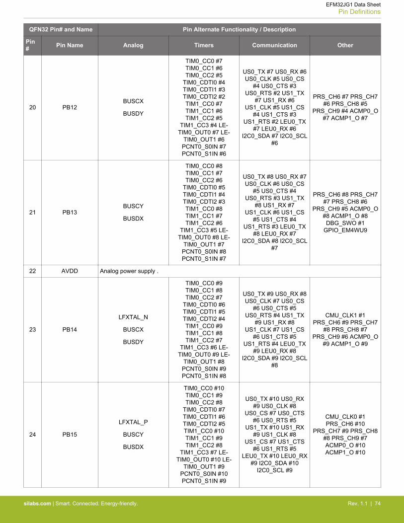
QFN32 Pin# and Name Pin Alternate Functionality / Description
Pin# Pin Name Analog Timers Communication Other
20 PB12BUSCX
BUSDY
TIM0_CC0 #7TIM0_CC1 #6TIM0_CC2 #5
TIM0_CDTI0 #4TIM0_CDTI1 #3TIM0_CDTI2 #2TIM1_CC0 #7TIM1_CC1 #6TIM1_CC2 #5
TIM1_CC3 #4 LE-TIM0_OUT0 #7 LE-
TIM0_OUT1 #6PCNT0_S0IN #7PCNT0_S1IN #6
US0_TX #7 US0_RX #6US0_CLK #5 US0_CS
#4 US0_CTS #3US0_RTS #2 US1_TX
#7 US1_RX #6US1_CLK #5 US1_CS
#4 US1_CTS #3US1_RTS #2 LEU0_TX
#7 LEU0_RX #6I2C0_SDA #7 I2C0_SCL
#6
PRS_CH6 #7 PRS_CH7#6 PRS_CH8 #5
PRS_CH9 #4 ACMP0_O#7 ACMP1_O #7
21 PB13BUSCY
BUSDX
TIM0_CC0 #8TIM0_CC1 #7TIM0_CC2 #6
TIM0_CDTI0 #5TIM0_CDTI1 #4TIM0_CDTI2 #3TIM1_CC0 #8TIM1_CC1 #7TIM1_CC2 #6
TIM1_CC3 #5 LE-TIM0_OUT0 #8 LE-
TIM0_OUT1 #7PCNT0_S0IN #8PCNT0_S1IN #7
US0_TX #8 US0_RX #7US0_CLK #6 US0_CS
#5 US0_CTS #4US0_RTS #3 US1_TX
#8 US1_RX #7US1_CLK #6 US1_CS
#5 US1_CTS #4US1_RTS #3 LEU0_TX
#8 LEU0_RX #7I2C0_SDA #8 I2C0_SCL
#7
PRS_CH6 #8 PRS_CH7#7 PRS_CH8 #6
PRS_CH9 #5 ACMP0_O#8 ACMP1_O #8DBG_SWO #1
GPIO_EM4WU9
22 AVDD Analog power supply .
23 PB14
LFXTAL_N
BUSCX
BUSDY
TIM0_CC0 #9TIM0_CC1 #8TIM0_CC2 #7
TIM0_CDTI0 #6TIM0_CDTI1 #5TIM0_CDTI2 #4TIM1_CC0 #9TIM1_CC1 #8TIM1_CC2 #7
TIM1_CC3 #6 LE-TIM0_OUT0 #9 LE-
TIM0_OUT1 #8PCNT0_S0IN #9PCNT0_S1IN #8
US0_TX #9 US0_RX #8US0_CLK #7 US0_CS
#6 US0_CTS #5US0_RTS #4 US1_TX
#9 US1_RX #8US1_CLK #7 US1_CS
#6 US1_CTS #5US1_RTS #4 LEU0_TX
#9 LEU0_RX #8I2C0_SDA #9 I2C0_SCL
#8
CMU_CLK1 #1PRS_CH6 #9 PRS_CH7
#8 PRS_CH8 #7PRS_CH9 #6 ACMP0_O
#9 ACMP1_O #9
24 PB15
LFXTAL_P
BUSCY
BUSDX
TIM0_CC0 #10TIM0_CC1 #9TIM0_CC2 #8
TIM0_CDTI0 #7TIM0_CDTI1 #6TIM0_CDTI2 #5TIM1_CC0 #10TIM1_CC1 #9TIM1_CC2 #8
TIM1_CC3 #7 LE-TIM0_OUT0 #10 LE-
TIM0_OUT1 #9PCNT0_S0IN #10PCNT0_S1IN #9
US0_TX #10 US0_RX#9 US0_CLK #8
US0_CS #7 US0_CTS#6 US0_RTS #5
US1_TX #10 US1_RX#9 US1_CLK #8
US1_CS #7 US1_CTS#6 US1_RTS #5
LEU0_TX #10 LEU0_RX#9 I2C0_SDA #10
I2C0_SCL #9
CMU_CLK0 #1PRS_CH6 #10
PRS_CH7 #9 PRS_CH8#8 PRS_CH9 #7ACMP0_O #10ACMP1_O #10
EFM32JG1 Data SheetPin Definitions
silabs.com | Smart. Connected. Energy-friendly. Rev. 1.1 | 74

QFN32 Pin# and Name Pin Alternate Functionality / Description
Pin# Pin Name Analog Timers Communication Other
25 VREGVSS Voltage regulator VSS
26 VREGSW DCDC regulator switching node
27 VREGVDD Voltage regulator VDD input
28 DVDD Digital power supply .
29 DECOUPLE Decouple output for on-chip voltage regulator. An external decoupling capacitor is required at this pin.
30 IOVDD Digital IO power supply .
31 PC10BUSAX
BUSBY
TIM0_CC0 #15TIM0_CC1 #14TIM0_CC2 #13
TIM0_CDTI0 #12TIM0_CDTI1 #11TIM0_CDTI2 #10TIM1_CC0 #15TIM1_CC1 #14TIM1_CC2 #13
TIM1_CC3 #12 LE-TIM0_OUT0 #15 LE-
TIM0_OUT1 #14PCNT0_S0IN #15PCNT0_S1IN #14
US0_TX #15 US0_RX#14 US0_CLK #13
US0_CS #12 US0_CTS#11 US0_RTS #10
US1_TX #15 US1_RX#14 US1_CLK #13
US1_CS #12 US1_CTS#11 US1_RTS #10
LEU0_TX #15 LEU0_RX#14 I2C0_SDA #15
I2C0_SCL #14
CMU_CLK1 #3PRS_CH0 #12PRS_CH9 #15PRS_CH10 #4PRS_CH11 #3ACMP0_O #15ACMP1_O #15
GPIO_EM4WU12
32 PC11BUSAY
BUSBX
TIM0_CC0 #16TIM0_CC1 #15TIM0_CC2 #14
TIM0_CDTI0 #13TIM0_CDTI1 #12TIM0_CDTI2 #11TIM1_CC0 #16TIM1_CC1 #15TIM1_CC2 #14
TIM1_CC3 #13 LE-TIM0_OUT0 #16 LE-
TIM0_OUT1 #15PCNT0_S0IN #16PCNT0_S1IN #15
US0_TX #16 US0_RX#15 US0_CLK #14
US0_CS #13 US0_CTS#12 US0_RTS #11
US1_TX #16 US1_RX#15 US1_CLK #14
US1_CS #13 US1_CTS#12 US1_RTS #11
LEU0_TX #16 LEU0_RX#15 I2C0_SDA #16
I2C0_SCL #15
CMU_CLK0 #3PRS_CH0 #13PRS_CH9 #16PRS_CH10 #5PRS_CH11 #4ACMP0_O #16ACMP1_O #16DBG_SWO #3
EFM32JG1 Data SheetPin Definitions
silabs.com | Smart. Connected. Energy-friendly. Rev. 1.1 | 75
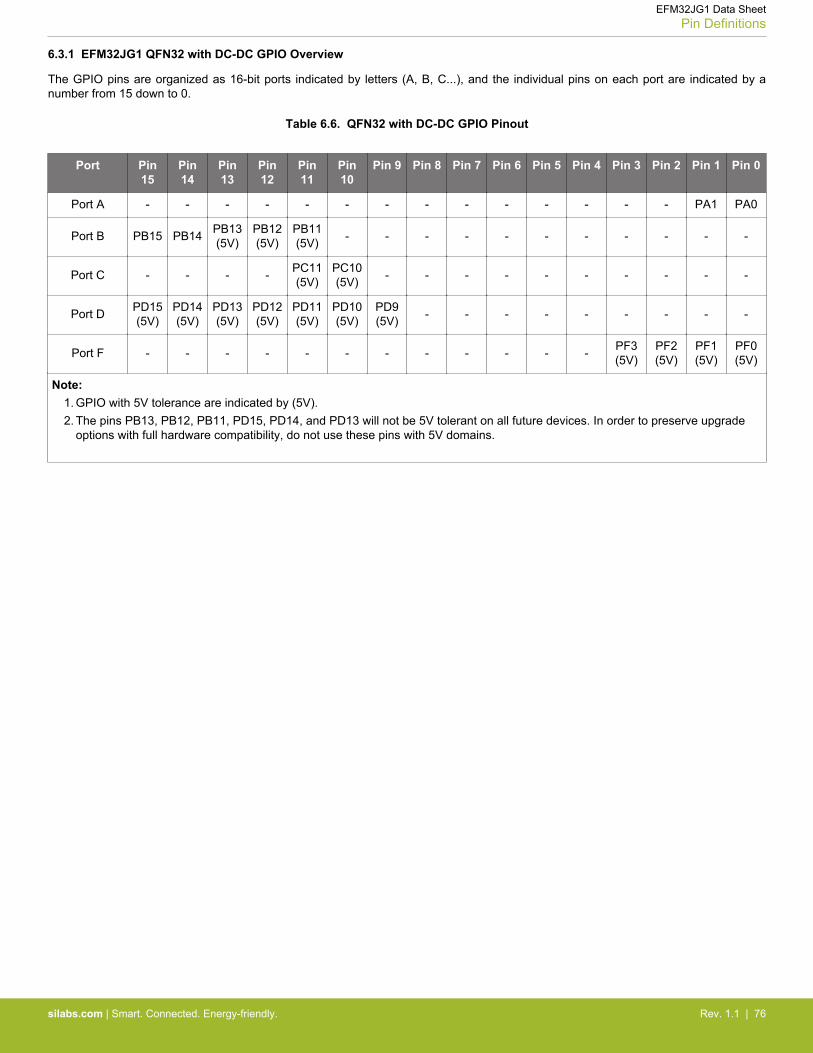
6.3.1 EFM32JG1 QFN32 with DC-DC GPIO Overview
The GPIO pins are organized as 16-bit ports indicated by letters (A, B, C...), and the individual pins on each port are indicated by anumber from 15 down to 0.
Table 6.6. QFN32 with DC-DC GPIO Pinout
Port Pin15
Pin14
Pin13
Pin12
Pin11
Pin10
Pin 9 Pin 8 Pin 7 Pin 6 Pin 5 Pin 4 Pin 3 Pin 2 Pin 1 Pin 0
Port A - - - - - - - - - - - - - - PA1 PA0
Port B PB15 PB14 PB13(5V)
PB12(5V)
PB11(5V) - - - - - - - - - - -
Port C - - - - PC11(5V)
PC10(5V) - - - - - - - - - -
Port D PD15(5V)
PD14(5V)
PD13(5V)
PD12(5V)
PD11(5V)
PD10(5V)
PD9(5V) - - - - - - - - -
Port F - - - - - - - - - - - - PF3(5V)
PF2(5V)
PF1(5V)
PF0(5V)
Note:1. GPIO with 5V tolerance are indicated by (5V).2. The pins PB13, PB12, PB11, PD15, PD14, and PD13 will not be 5V tolerant on all future devices. In order to preserve upgrade
options with full hardware compatibility, do not use these pins with 5V domains.
EFM32JG1 Data SheetPin Definitions
silabs.com | Smart. Connected. Energy-friendly. Rev. 1.1 | 76
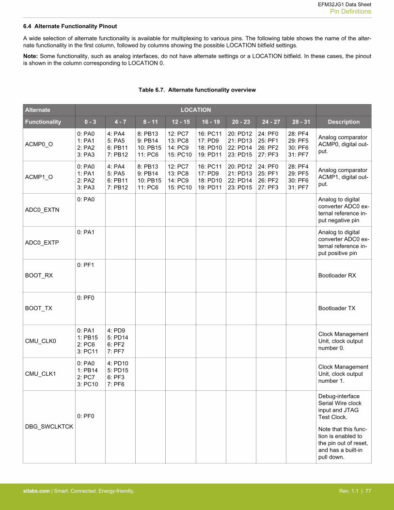
6.4 Alternate Functionality Pinout
A wide selection of alternate functionality is available for multiplexing to various pins. The following table shows the name of the alter-nate functionality in the first column, followed by columns showing the possible LOCATION bitfield settings.
Note: Some functionality, such as analog interfaces, do not have alternate settings or a LOCATION bitfield. In these cases, the pinoutis shown in the column corresponding to LOCATION 0.
Table 6.7. Alternate functionality overview
Alternate LOCATION
Functionality 0 - 3 4 - 7 8 - 11 12 - 15 16 - 19 20 - 23 24 - 27 28 - 31 Description
ACMP0_O
0: PA01: PA12: PA23: PA3
4: PA45: PA56: PB117: PB12
8: PB139: PB1410: PB1511: PC6
12: PC713: PC814: PC915: PC10
16: PC1117: PD918: PD1019: PD11
20: PD1221: PD1322: PD1423: PD15
24: PF025: PF126: PF227: PF3
28: PF429: PF530: PF631: PF7
Analog comparatorACMP0, digital out-put.
ACMP1_O
0: PA01: PA12: PA23: PA3
4: PA45: PA56: PB117: PB12
8: PB139: PB1410: PB1511: PC6
12: PC713: PC814: PC915: PC10
16: PC1117: PD918: PD1019: PD11
20: PD1221: PD1322: PD1423: PD15
24: PF025: PF126: PF227: PF3
28: PF429: PF530: PF631: PF7
Analog comparatorACMP1, digital out-put.
ADC0_EXTN
0: PA0 Analog to digitalconverter ADC0 ex-ternal reference in-put negative pin
ADC0_EXTP
0: PA1 Analog to digitalconverter ADC0 ex-ternal reference in-put positive pin
BOOT_RX
0: PF1
Bootloader RX
BOOT_TX
0: PF0
Bootloader TX
CMU_CLK0
0: PA11: PB152: PC63: PC11
4: PD95: PD146: PF27: PF7
Clock ManagementUnit, clock outputnumber 0.
CMU_CLK1
0: PA01: PB142: PC73: PC10
4: PD105: PD156: PF37: PF6
Clock ManagementUnit, clock outputnumber 1.
DBG_SWCLKTCK
0: PF0
Debug-interfaceSerial Wire clockinput and JTAGTest Clock.
Note that this func-tion is enabled tothe pin out of reset,and has a built-inpull down.
EFM32JG1 Data SheetPin Definitions
silabs.com | Smart. Connected. Energy-friendly. Rev. 1.1 | 77

Alternate LOCATION
Functionality 0 - 3 4 - 7 8 - 11 12 - 15 16 - 19 20 - 23 24 - 27 28 - 31 Description
DBG_SWDIOTMS
0: PF1
Debug-interfaceSerial Wire data in-put / output andJTAG Test ModeSelect.
Note that this func-tion is enabled tothe pin out of reset,and has a built-inpull up.
DBG_SWO
0: PF21: PB132: PD153: PC11
Debug-interfaceSerial Wire viewerOutput.
Note that this func-tion is not enabledafter reset, andmust be enabled bysoftware to beused.
DBG_TDI
0: PF3
Debug-interfaceJTAG Test Data In.
Note that this func-tion is enabled topin out of reset,and has a built-inpull up.
DBG_TDO
0: PF2Debug-interfaceJTAG Test DataOut.
Note that this func-tion is enabled topin out of reset.
GPIO_EM4WU0
0: PF2 Pin can be used towake the systemup from EM4
GPIO_EM4WU1
0: PF7 Pin can be used towake the systemup from EM4
GPIO_EM4WU4
0: PD14 Pin can be used towake the systemup from EM4
GPIO_EM4WU8
0: PA3 Pin can be used towake the systemup from EM4
GPIO_EM4WU9
0: PB13 Pin can be used towake the systemup from EM4
EFM32JG1 Data SheetPin Definitions
silabs.com | Smart. Connected. Energy-friendly. Rev. 1.1 | 78

Alternate LOCATION
Functionality 0 - 3 4 - 7 8 - 11 12 - 15 16 - 19 20 - 23 24 - 27 28 - 31 Description
GPIO_EM4WU12
0: PC10 Pin can be used towake the systemup from EM4
I2C0_SCL
0: PA11: PA22: PA33: PA4
4: PA55: PB116: PB127: PB13
8: PB149: PB1510: PC611: PC7
12: PC813: PC914: PC1015: PC11
16: PD917: PD1018: PD1119: PD12
20: PD1321: PD1422: PD1523: PF0
24: PF125: PF226: PF327: PF4
28: PF529: PF630: PF731: PA0
I2C0 Serial ClockLine input / output.
I2C0_SDA
0: PA01: PA12: PA23: PA3
4: PA45: PA56: PB117: PB12
8: PB139: PB1410: PB1511: PC6
12: PC713: PC814: PC915: PC10
16: PC1117: PD918: PD1019: PD11
20: PD1221: PD1322: PD1423: PD15
24: PF025: PF126: PF227: PF3
28: PF429: PF530: PF631: PF7
I2C0 Serial Data in-put / output.
LETIM0_OUT0
0: PA01: PA12: PA23: PA3
4: PA45: PA56: PB117: PB12
8: PB139: PB1410: PB1511: PC6
12: PC713: PC814: PC915: PC10
16: PC1117: PD918: PD1019: PD11
20: PD1221: PD1322: PD1423: PD15
24: PF025: PF126: PF227: PF3
28: PF429: PF530: PF631: PF7
Low Energy TimerLETIM0, outputchannel 0.
LETIM0_OUT1
0: PA11: PA22: PA33: PA4
4: PA55: PB116: PB127: PB13
8: PB149: PB1510: PC611: PC7
12: PC813: PC914: PC1015: PC11
16: PD917: PD1018: PD1119: PD12
20: PD1321: PD1422: PD1523: PF0
24: PF125: PF226: PF327: PF4
28: PF529: PF630: PF731: PA0
Low Energy TimerLETIM0, outputchannel 1.
LEU0_RX
0: PA11: PA22: PA33: PA4
4: PA55: PB116: PB127: PB13
8: PB149: PB1510: PC611: PC7
12: PC813: PC914: PC1015: PC11
16: PD917: PD1018: PD1119: PD12
20: PD1321: PD1422: PD1523: PF0
24: PF125: PF226: PF327: PF4
28: PF529: PF630: PF731: PA0
LEUART0 Receiveinput.
LEU0_TX
0: PA01: PA12: PA23: PA3
4: PA45: PA56: PB117: PB12
8: PB139: PB1410: PB1511: PC6
12: PC713: PC814: PC915: PC10
16: PC1117: PD918: PD1019: PD11
20: PD1221: PD1322: PD1423: PD15
24: PF025: PF126: PF227: PF3
28: PF429: PF530: PF631: PF7
LEUART0 Transmitoutput. Also usedas receive input inhalf duplex commu-nication.
LFXTAL_N
0: PB14
Low FrequencyCrystal (typically32.768 kHz) nega-tive pin. Also usedas an optional ex-ternal clock inputpin.
LFXTAL_P
0: PB15 Low FrequencyCrystal (typically32.768 kHz) posi-tive pin.
PCNT0_S0IN
0: PA01: PA12: PA23: PA3
4: PA45: PA56: PB117: PB12
8: PB139: PB1410: PB1511: PC6
12: PC713: PC814: PC915: PC10
16: PC1117: PD918: PD1019: PD11
20: PD1221: PD1322: PD1423: PD15
24: PF025: PF126: PF227: PF3
28: PF429: PF530: PF631: PF7
Pulse CounterPCNT0 input num-ber 0.
PCNT0_S1IN
0: PA11: PA22: PA33: PA4
4: PA55: PB116: PB127: PB13
8: PB149: PB1510: PC611: PC7
12: PC813: PC914: PC1015: PC11
16: PD917: PD1018: PD1119: PD12
20: PD1321: PD1422: PD1523: PF0
24: PF125: PF226: PF327: PF4
28: PF529: PF630: PF731: PA0
Pulse CounterPCNT0 input num-ber 1.
PRS_CH0
0: PF01: PF12: PF23: PF3
4: PF45: PF56: PF67: PF7
8: PC69: PC710: PC811: PC9
12: PC1013: PC11 Peripheral Reflex
System PRS, chan-nel 0.
EFM32JG1 Data SheetPin Definitions
silabs.com | Smart. Connected. Energy-friendly. Rev. 1.1 | 79
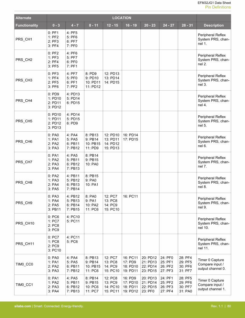
Alternate LOCATION
Functionality 0 - 3 4 - 7 8 - 11 12 - 15 16 - 19 20 - 23 24 - 27 28 - 31 Description
PRS_CH1
0: PF11: PF22: PF33: PF4
4: PF55: PF66: PF77: PF0
Peripheral ReflexSystem PRS, chan-nel 1.
PRS_CH2
0: PF21: PF32: PF43: PF5
4: PF65: PF76: PF07: PF1
Peripheral ReflexSystem PRS, chan-nel 2.
PRS_CH3
0: PF31: PF42: PF53: PF6
4: PF75: PF06: PF17: PF2
8: PD99: PD1010: PD1111: PD12
12: PD1313: PD1414: PD15
Peripheral ReflexSystem PRS, chan-nel 3.
PRS_CH4
0: PD91: PD102: PD113: PD12
4: PD135: PD146: PD15
Peripheral ReflexSystem PRS, chan-nel 4.
PRS_CH5
0: PD101: PD112: PD123: PD13
4: PD145: PD156: PD9
Peripheral ReflexSystem PRS, chan-nel 5.
PRS_CH6
0: PA01: PA12: PA23: PA3
4: PA45: PA56: PB117: PB12
8: PB139: PB1410: PB1511: PD9
12: PD1013: PD1114: PD1215: PD13
16: PD1417: PD15 Peripheral Reflex
System PRS, chan-nel 6.
PRS_CH7
0: PA11: PA22: PA33: PA4
4: PA55: PB116: PB127: PB13
8: PB149: PB1510: PA0
Peripheral ReflexSystem PRS, chan-nel 7.
PRS_CH8
0: PA21: PA32: PA43: PA5
4: PB115: PB126: PB137: PB14
8: PB159: PA010: PA1
Peripheral ReflexSystem PRS, chan-nel 8.
PRS_CH9
0: PA31: PA42: PA53: PB11
4: PB125: PB136: PB147: PB15
8: PA09: PA110: PA211: PC6
12: PC713: PC814: PC915: PC10
16: PC11 Peripheral ReflexSystem PRS, chan-nel 9.
PRS_CH10
0: PC61: PC72: PC83: PC9
4: PC105: PC11 Peripheral Reflex
System PRS, chan-nel 10.
PRS_CH11
0: PC71: PC82: PC93: PC10
4: PC115: PC6 Peripheral Reflex
System PRS, chan-nel 11.
TIM0_CC0
0: PA01: PA12: PA23: PA3
4: PA45: PA56: PB117: PB12
8: PB139: PB1410: PB1511: PC6
12: PC713: PC814: PC915: PC10
16: PC1117: PD918: PD1019: PD11
20: PD1221: PD1322: PD1423: PD15
24: PF025: PF126: PF227: PF3
28: PF429: PF530: PF631: PF7
Timer 0 CaptureCompare input /output channel 0.
TIM0_CC1
0: PA11: PA22: PA33: PA4
4: PA55: PB116: PB127: PB13
8: PB149: PB1510: PC611: PC7
12: PC813: PC914: PC1015: PC11
16: PD917: PD1018: PD1119: PD12
20: PD1321: PD1422: PD1523: PF0
24: PF125: PF226: PF327: PF4
28: PF529: PF630: PF731: PA0
Timer 0 CaptureCompare input /output channel 1.
EFM32JG1 Data SheetPin Definitions
silabs.com | Smart. Connected. Energy-friendly. Rev. 1.1 | 80

Alternate LOCATION
Functionality 0 - 3 4 - 7 8 - 11 12 - 15 16 - 19 20 - 23 24 - 27 28 - 31 Description
TIM0_CC2
0: PA21: PA32: PA43: PA5
4: PB115: PB126: PB137: PB14
8: PB159: PC610: PC711: PC8
12: PC913: PC1014: PC1115: PD9
16: PD1017: PD1118: PD1219: PD13
20: PD1421: PD1522: PF023: PF1
24: PF225: PF326: PF427: PF5
28: PF629: PF730: PA031: PA1
Timer 0 CaptureCompare input /output channel 2.
TIM0_CDTI0
0: PA31: PA42: PA53: PB11
4: PB125: PB136: PB147: PB15
8: PC69: PC710: PC811: PC9
12: PC1013: PC1114: PD915: PD10
16: PD1117: PD1218: PD1319: PD14
20: PD1521: PF022: PF123: PF2
24: PF325: PF426: PF527: PF6
28: PF729: PA030: PA131: PA2
Timer 0 Compli-mentary Dead TimeInsertion channel 0.
TIM0_CDTI1
0: PA41: PA52: PB113: PB12
4: PB135: PB146: PB157: PC6
8: PC79: PC810: PC911: PC10
12: PC1113: PD914: PD1015: PD11
16: PD1217: PD1318: PD1419: PD15
20: PF021: PF122: PF223: PF3
24: PF425: PF526: PF627: PF7
28: PA029: PA130: PA231: PA3
Timer 0 Compli-mentary Dead TimeInsertion channel 1.
TIM0_CDTI2
0: PA51: PB112: PB123: PB13
4: PB145: PB156: PC67: PC7
8: PC89: PC910: PC1011: PC11
12: PD913: PD1014: PD1115: PD12
16: PD1317: PD1418: PD1519: PF0
20: PF121: PF222: PF323: PF4
24: PF525: PF626: PF727: PA0
28: PA129: PA230: PA331: PA4
Timer 0 Compli-mentary Dead TimeInsertion channel 2.
TIM1_CC0
0: PA01: PA12: PA23: PA3
4: PA45: PA56: PB117: PB12
8: PB139: PB1410: PB1511: PC6
12: PC713: PC814: PC915: PC10
16: PC1117: PD918: PD1019: PD11
20: PD1221: PD1322: PD1423: PD15
24: PF025: PF126: PF227: PF3
28: PF429: PF530: PF631: PF7
Timer 1 CaptureCompare input /output channel 0.
TIM1_CC1
0: PA11: PA22: PA33: PA4
4: PA55: PB116: PB127: PB13
8: PB149: PB1510: PC611: PC7
12: PC813: PC914: PC1015: PC11
16: PD917: PD1018: PD1119: PD12
20: PD1321: PD1422: PD1523: PF0
24: PF125: PF226: PF327: PF4
28: PF529: PF630: PF731: PA0
Timer 1 CaptureCompare input /output channel 1.
TIM1_CC2
0: PA21: PA32: PA43: PA5
4: PB115: PB126: PB137: PB14
8: PB159: PC610: PC711: PC8
12: PC913: PC1014: PC1115: PD9
16: PD1017: PD1118: PD1219: PD13
20: PD1421: PD1522: PF023: PF1
24: PF225: PF326: PF427: PF5
28: PF629: PF730: PA031: PA1
Timer 1 CaptureCompare input /output channel 2.
TIM1_CC3
0: PA31: PA42: PA53: PB11
4: PB125: PB136: PB147: PB15
8: PC69: PC710: PC811: PC9
12: PC1013: PC1114: PD915: PD10
16: PD1117: PD1218: PD1319: PD14
20: PD1521: PF022: PF123: PF2
24: PF325: PF426: PF527: PF6
28: PF729: PA030: PA131: PA2
Timer 1 CaptureCompare input /output channel 3.
US0_CLK
0: PA21: PA32: PA43: PA5
4: PB115: PB126: PB137: PB14
8: PB159: PC610: PC711: PC8
12: PC913: PC1014: PC1115: PD9
16: PD1017: PD1118: PD1219: PD13
20: PD1421: PD1522: PF023: PF1
24: PF225: PF326: PF427: PF5
28: PF629: PF730: PA031: PA1
USART0 clock in-put / output.
US0_CS
0: PA31: PA42: PA53: PB11
4: PB125: PB136: PB147: PB15
8: PC69: PC710: PC811: PC9
12: PC1013: PC1114: PD915: PD10
16: PD1117: PD1218: PD1319: PD14
20: PD1521: PF022: PF123: PF2
24: PF325: PF426: PF527: PF6
28: PF729: PA030: PA131: PA2
USART0 chip se-lect input / output.
US0_CTS
0: PA41: PA52: PB113: PB12
4: PB135: PB146: PB157: PC6
8: PC79: PC810: PC911: PC10
12: PC1113: PD914: PD1015: PD11
16: PD1217: PD1318: PD1419: PD15
20: PF021: PF122: PF223: PF3
24: PF425: PF526: PF627: PF7
28: PA029: PA130: PA231: PA3
USART0 Clear ToSend hardwareflow control input.
US0_RTS
0: PA51: PB112: PB123: PB13
4: PB145: PB156: PC67: PC7
8: PC89: PC910: PC1011: PC11
12: PD913: PD1014: PD1115: PD12
16: PD1317: PD1418: PD1519: PF0
20: PF121: PF222: PF323: PF4
24: PF525: PF626: PF727: PA0
28: PA129: PA230: PA331: PA4
USART0 RequestTo Send hardwareflow control output.
EFM32JG1 Data SheetPin Definitions
silabs.com | Smart. Connected. Energy-friendly. Rev. 1.1 | 81
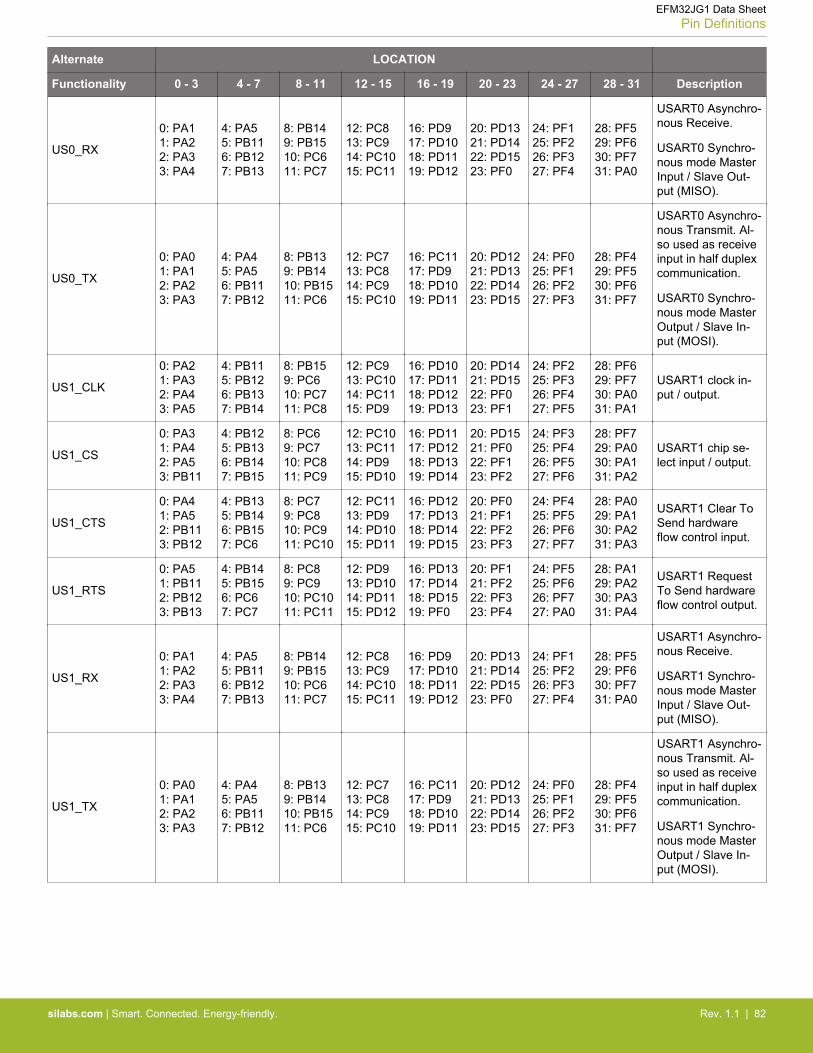
Alternate LOCATION
Functionality 0 - 3 4 - 7 8 - 11 12 - 15 16 - 19 20 - 23 24 - 27 28 - 31 Description
US0_RX
0: PA11: PA22: PA33: PA4
4: PA55: PB116: PB127: PB13
8: PB149: PB1510: PC611: PC7
12: PC813: PC914: PC1015: PC11
16: PD917: PD1018: PD1119: PD12
20: PD1321: PD1422: PD1523: PF0
24: PF125: PF226: PF327: PF4
28: PF529: PF630: PF731: PA0
USART0 Asynchro-nous Receive.
USART0 Synchro-nous mode MasterInput / Slave Out-put (MISO).
US0_TX
0: PA01: PA12: PA23: PA3
4: PA45: PA56: PB117: PB12
8: PB139: PB1410: PB1511: PC6
12: PC713: PC814: PC915: PC10
16: PC1117: PD918: PD1019: PD11
20: PD1221: PD1322: PD1423: PD15
24: PF025: PF126: PF227: PF3
28: PF429: PF530: PF631: PF7
USART0 Asynchro-nous Transmit. Al-so used as receiveinput in half duplexcommunication.
USART0 Synchro-nous mode MasterOutput / Slave In-put (MOSI).
US1_CLK
0: PA21: PA32: PA43: PA5
4: PB115: PB126: PB137: PB14
8: PB159: PC610: PC711: PC8
12: PC913: PC1014: PC1115: PD9
16: PD1017: PD1118: PD1219: PD13
20: PD1421: PD1522: PF023: PF1
24: PF225: PF326: PF427: PF5
28: PF629: PF730: PA031: PA1
USART1 clock in-put / output.
US1_CS
0: PA31: PA42: PA53: PB11
4: PB125: PB136: PB147: PB15
8: PC69: PC710: PC811: PC9
12: PC1013: PC1114: PD915: PD10
16: PD1117: PD1218: PD1319: PD14
20: PD1521: PF022: PF123: PF2
24: PF325: PF426: PF527: PF6
28: PF729: PA030: PA131: PA2
USART1 chip se-lect input / output.
US1_CTS
0: PA41: PA52: PB113: PB12
4: PB135: PB146: PB157: PC6
8: PC79: PC810: PC911: PC10
12: PC1113: PD914: PD1015: PD11
16: PD1217: PD1318: PD1419: PD15
20: PF021: PF122: PF223: PF3
24: PF425: PF526: PF627: PF7
28: PA029: PA130: PA231: PA3
USART1 Clear ToSend hardwareflow control input.
US1_RTS
0: PA51: PB112: PB123: PB13
4: PB145: PB156: PC67: PC7
8: PC89: PC910: PC1011: PC11
12: PD913: PD1014: PD1115: PD12
16: PD1317: PD1418: PD1519: PF0
20: PF121: PF222: PF323: PF4
24: PF525: PF626: PF727: PA0
28: PA129: PA230: PA331: PA4
USART1 RequestTo Send hardwareflow control output.
US1_RX
0: PA11: PA22: PA33: PA4
4: PA55: PB116: PB127: PB13
8: PB149: PB1510: PC611: PC7
12: PC813: PC914: PC1015: PC11
16: PD917: PD1018: PD1119: PD12
20: PD1321: PD1422: PD1523: PF0
24: PF125: PF226: PF327: PF4
28: PF529: PF630: PF731: PA0
USART1 Asynchro-nous Receive.
USART1 Synchro-nous mode MasterInput / Slave Out-put (MISO).
US1_TX
0: PA01: PA12: PA23: PA3
4: PA45: PA56: PB117: PB12
8: PB139: PB1410: PB1511: PC6
12: PC713: PC814: PC915: PC10
16: PC1117: PD918: PD1019: PD11
20: PD1221: PD1322: PD1423: PD15
24: PF025: PF126: PF227: PF3
28: PF429: PF530: PF631: PF7
USART1 Asynchro-nous Transmit. Al-so used as receiveinput in half duplexcommunication.
USART1 Synchro-nous mode MasterOutput / Slave In-put (MOSI).
EFM32JG1 Data SheetPin Definitions
silabs.com | Smart. Connected. Energy-friendly. Rev. 1.1 | 82
6.5 Analog Port (APORT) Client Maps
The Analog Port (APORT) is an infrastructure used to connect chip pins with on-chip analog clients such as analog comparators, ADCs,DACs, etc. The APORT consists of a set of shared buses, switches, and control logic needed to configurably implement the signal rout-ing. A complete description of APORT functionality can be found in the Reference Manual.
Client maps for each analog circuit using the APORT are shown in the following tables. The maps are organized by bus, and show theperipheral's port connection, the shared bus, and the connection from specific bus channel numbers to GPIO pins.
In general, enumerations for the pin selection field in an analog peripheral's register can be determined by finding the desired pin con-nection in the table and then combining the value in the Port column (APORT__), and the channel identifier (CH__). For example, if pinPF7 is available on port APORT2X as CH23, the register field enumeration to connect to PF7 would be APORT2XCH23. The sharedbus used by this connection is indicated in the Bus column.
Table 6.8. ACMP0 Bus and Pin Mapping
Port
Bus
CH
31
CH
30
CH
29
CH
28
CH
27
CH
26
CH
25
CH
24
CH
23
CH
22
CH
21
CH
20
CH
19
CH
18
CH
17
CH
16
CH
15
CH
14
CH
13
CH
12
CH
11
CH
10
CH
9
CH
8
CH
7
CH
6
CH
5
CH
4
CH
3
CH
2
CH
1
CH
0
AP
OR
T1X
BU
SA
X
PF6
PF4
PF2
PF0
PC
10
PC
8
PC
6
AP
OR
T1Y
BU
SA
Y
PF7
PF5
PF3
PF1
PC
11
PC
9
PC
7
AP
OR
T2X
BU
SB
X
PF7
PF5
PF3
PF1
PC
11
PC
9
PC
7
AP
OR
T2Y
BU
SB
Y
PF6
PF4
PF2
PF0
PC
10
PC
8
PC
6
AP
OR
T3X
BU
SC
X
PB
14
PB
12
PA
4
PA
2
PA
0
PD
14
PD
12
PD
10
AP
OR
T3Y
BU
SC
Y
PB
15
PB
13
PB
11
PA
5
PA
3
PA
1
PD
15
PD
13
PD
11
PD
9
AP
OR
T4X
BU
SD
X
PB
15
PB
13
PB
11
PA
5
PA
3
PA
1
PD
15
PD
13
PD
11
PD
9
AP
OR
T4Y
BU
SD
Y
PB
14
PB
12
PA
4
PA
2
PA
0
PD
14
PD
12
PD
10
EFM32JG1 Data SheetPin Definitions
silabs.com | Smart. Connected. Energy-friendly. Rev. 1.1 | 83

Table 6.9. ACMP1 Bus and Pin MappingPo
rt
Bus
CH
31
CH
30
CH
29
CH
28
CH
27
CH
26
CH
25
CH
24
CH
23
CH
22
CH
21
CH
20
CH
19
CH
18
CH
17
CH
16
CH
15
CH
14
CH
13
CH
12
CH
11
CH
10
CH
9
CH
8
CH
7
CH
6
CH
5
CH
4
CH
3
CH
2
CH
1
CH
0
AP
OR
T1X
BU
SA
X
PF6
PF4
PF2
PF0
PC
10
PC
8
PC
6
AP
OR
T1Y
BU
SA
Y
PF7
PF5
PF3
PF1
PC
11
PC
9
PC
7
AP
OR
T2X
BU
SB
X
PF7
PF5
PF3
PF1
PC
11
PC
9
PC
7
AP
OR
T2Y
BU
SB
Y
PF6
PF4
PF2
PF0
PC
10
PC
8
PC
6
AP
OR
T3X
BU
SC
X
PB
14
PB
12
PA
4
PA
2
PA
0
PD
14
PD
12
PD
10
AP
OR
T3Y
BU
SC
Y
PB
15
PB
13
PB
11
PA
5
PA
3
PA
1
PD
15
PD
13
PD
11
PD
9
AP
OR
T4X
BU
SD
X
PB
15
PB
13
PB
11
PA
5
PA
3
PA
1
PD
15
PD
13
PD
11
PD
9
AP
OR
T4Y
BU
SD
Y
PB
14
PB
12
PA
4
PA
2
PA
0
PD
14
PD
12
PD
10
EFM32JG1 Data SheetPin Definitions
silabs.com | Smart. Connected. Energy-friendly. Rev. 1.1 | 84
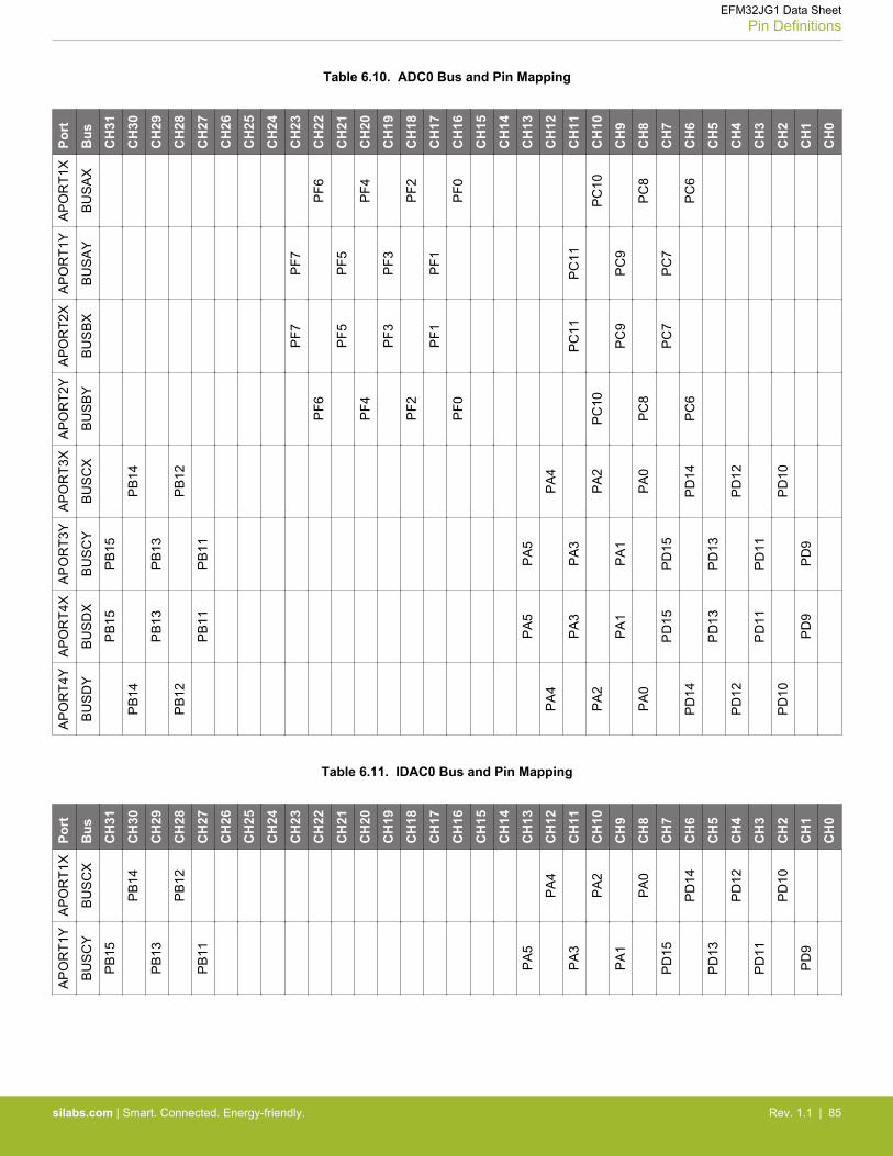
Table 6.10. ADC0 Bus and Pin MappingPo
rt
Bus
CH
31
CH
30
CH
29
CH
28
CH
27
CH
26
CH
25
CH
24
CH
23
CH
22
CH
21
CH
20
CH
19
CH
18
CH
17
CH
16
CH
15
CH
14
CH
13
CH
12
CH
11
CH
10
CH
9
CH
8
CH
7
CH
6
CH
5
CH
4
CH
3
CH
2
CH
1
CH
0
AP
OR
T1X
BU
SA
X
PF6
PF4
PF2
PF0
PC
10
PC
8
PC
6
AP
OR
T1Y
BU
SA
Y
PF7
PF5
PF3
PF1
PC
11
PC
9
PC
7
AP
OR
T2X
BU
SB
X
PF7
PF5
PF3
PF1
PC
11
PC
9
PC
7
AP
OR
T2Y
BU
SB
Y
PF6
PF4
PF2
PF0
PC
10
PC
8
PC
6
AP
OR
T3X
BU
SC
X
PB
14
PB
12
PA
4
PA
2
PA
0
PD
14
PD
12
PD
10
AP
OR
T3Y
BU
SC
Y
PB
15
PB
13
PB
11
PA
5
PA
3
PA
1
PD
15
PD
13
PD
11
PD
9
AP
OR
T4X
BU
SD
X
PB
15
PB
13
PB
11
PA
5
PA
3
PA
1
PD
15
PD
13
PD
11
PD
9
AP
OR
T4Y
BU
SD
Y
PB
14
PB
12
PA
4
PA
2
PA
0
PD
14
PD
12
PD
10Table 6.11. IDAC0 Bus and Pin Mapping
Port
Bus
CH
31
CH
30
CH
29
CH
28
CH
27
CH
26
CH
25
CH
24
CH
23
CH
22
CH
21
CH
20
CH
19
CH
18
CH
17
CH
16
CH
15
CH
14
CH
13
CH
12
CH
11
CH
10
CH
9
CH
8
CH
7
CH
6
CH
5
CH
4
CH
3
CH
2
CH
1
CH
0
AP
OR
T1X
BU
SC
X
PB
14
PB
12
PA
4
PA
2
PA
0
PD
14
PD
12
PD
10
AP
OR
T1Y
BU
SC
Y
PB
15
PB
13
PB
11
PA
5
PA
3
PA
1
PD
15
PD
13
PD
11
PD
9
EFM32JG1 Data SheetPin Definitions
silabs.com | Smart. Connected. Energy-friendly. Rev. 1.1 | 85

7. QFN48 Package Specifications
7.1 QFN48 Package Dimensions
Figure 7.1. QFN48 Package Drawing
EFM32JG1 Data SheetQFN48 Package Specifications
silabs.com | Smart. Connected. Energy-friendly. Rev. 1.1 | 86

Table 7.1. QFN48 Package Dimensions
Dimension Min Typ Max
A 0.80 0.85 0.90
A1 0.00 0.02 0.05
A3 0.20 REF
b 0.18 0.25 0.30
D 6.90 7.00 7.10
E 6.90 7.00 7.10
D2 4.60 4.70 4.80
E2 4.60 4.70 4.80
e 0.50 BSC
L 0.30 0.40 0.50
K 0.20 — —
R 0.09 — 0.14
aaa 0.15
bbb 0.10
ccc 0.10
ddd 0.05
eee 0.08
fff 0.10
Note:1. All dimensions shown are in millimeters (mm) unless otherwise noted.2. Dimensioning and Tolerancing per ANSI Y14.5M-1994.3. This drawing conforms to the JEDEC Solid State Outline MO-220, Variation VKKD-4.4. Recommended card reflow profile is per the JEDEC/IPC J-STD-020 specification for Small Body Components.
EFM32JG1 Data SheetQFN48 Package Specifications
silabs.com | Smart. Connected. Energy-friendly. Rev. 1.1 | 87
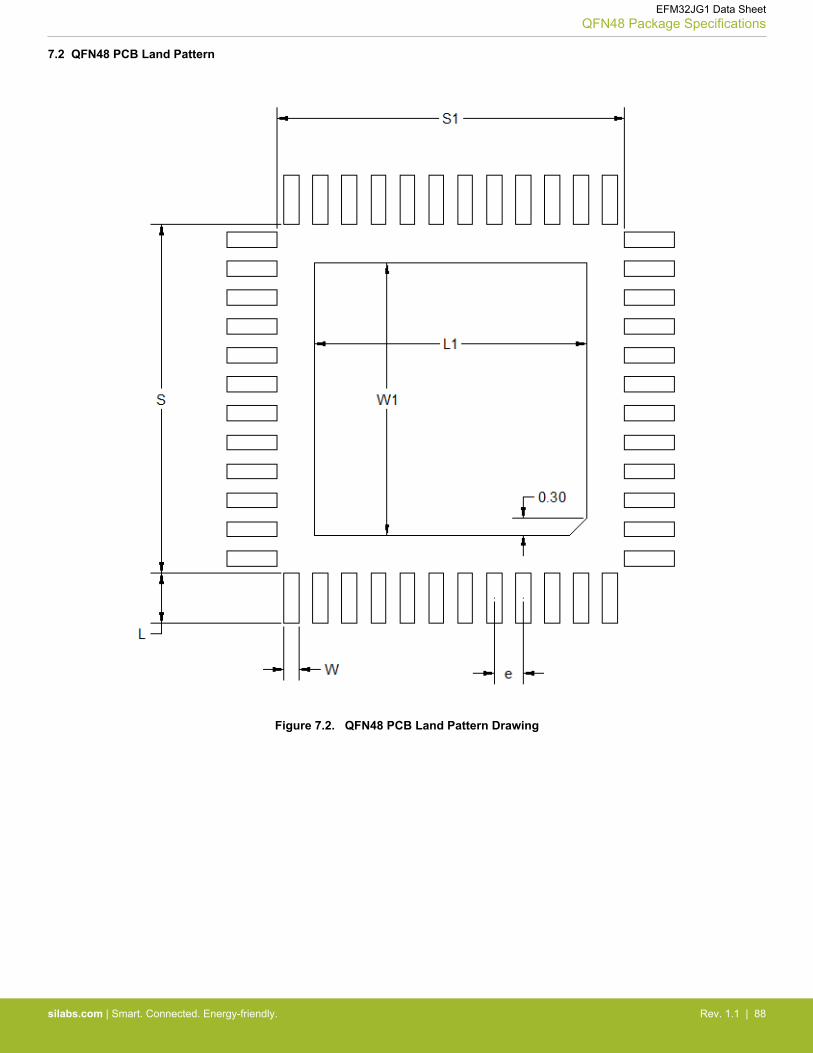
7.2 QFN48 PCB Land Pattern
Figure 7.2. QFN48 PCB Land Pattern Drawing
EFM32JG1 Data SheetQFN48 Package Specifications
silabs.com | Smart. Connected. Energy-friendly. Rev. 1.1 | 88

Table 7.2. QFN48 PCB Land Pattern Dimensions
Dimension Typ
S1 6.01
S 6.01
L1 4.70
W1 4.70
e 0.50
W 0.26
L 0.86
Note:1. All dimensions shown are in millimeters (mm) unless otherwise noted.2. This Land Pattern Design is based on the IPC-7351 guidelines.3. All metal pads are to be non-solder mask defined (NSMD). Clearance between the solder mask and the metal pad is to be 60 µm
minimum, all the way around the pad.4. A stainless steel, laser-cut and electro-polished stencil with trapezoidal walls should be used to assure good solder paste release.5. The stencil thickness should be 0.125 mm (5 mils).6. The ratio of stencil aperture to land pad size can be 1:1 for all perimeter pads.7. A 4x4 array of 0.75 mm square openings on a 1.00 mm pitch can be used for the center ground pad.8. A No-Clean, Type-3 solder paste is recommended.9. The recommended card reflow profile is per the JEDEC/IPC J-STD-020 specification for Small Body Components.
EFM32JG1 Data SheetQFN48 Package Specifications
silabs.com | Smart. Connected. Energy-friendly. Rev. 1.1 | 89

7.3 QFN48 Package Marking
PPPPPPPPPTTTTTTYYWW #
EFM32
Figure 7.3. QFN48 Package Marking
The package marking consists of:• PPPPPPPPP – The part number designation.• TTTTTT – A trace or manufacturing code. The first letter is the device revision.• YY – The last 2 digits of the assembly year.• WW – The 2-digit workweek when the device was assembled.• # – Reserved for future use. Current value is 0.
EFM32JG1 Data SheetQFN48 Package Specifications
silabs.com | Smart. Connected. Energy-friendly. Rev. 1.1 | 90

8. QFN32 Package Specifications
8.1 QFN32 Package Dimensions
Figure 8.1. QFN32 Package Drawing
EFM32JG1 Data SheetQFN32 Package Specifications
silabs.com | Smart. Connected. Energy-friendly. Rev. 1.1 | 91
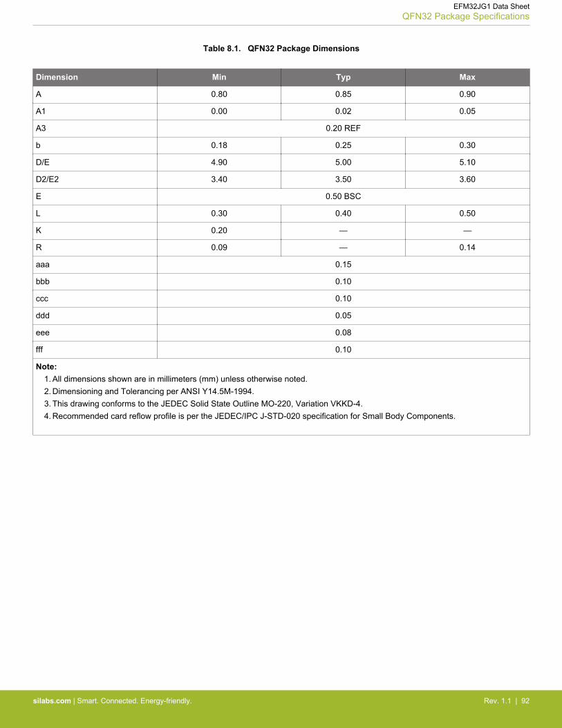
Table 8.1. QFN32 Package Dimensions
Dimension Min Typ Max
A 0.80 0.85 0.90
A1 0.00 0.02 0.05
A3 0.20 REF
b 0.18 0.25 0.30
D/E 4.90 5.00 5.10
D2/E2 3.40 3.50 3.60
E 0.50 BSC
L 0.30 0.40 0.50
K 0.20 — —
R 0.09 — 0.14
aaa 0.15
bbb 0.10
ccc 0.10
ddd 0.05
eee 0.08
fff 0.10
Note:1. All dimensions shown are in millimeters (mm) unless otherwise noted.2. Dimensioning and Tolerancing per ANSI Y14.5M-1994.3. This drawing conforms to the JEDEC Solid State Outline MO-220, Variation VKKD-4.4. Recommended card reflow profile is per the JEDEC/IPC J-STD-020 specification for Small Body Components.
EFM32JG1 Data SheetQFN32 Package Specifications
silabs.com | Smart. Connected. Energy-friendly. Rev. 1.1 | 92

8.2 QFN32 PCB Land Pattern
Figure 8.2. QFN32 PCB Land Pattern Drawing
EFM32JG1 Data SheetQFN32 Package Specifications
silabs.com | Smart. Connected. Energy-friendly. Rev. 1.1 | 93
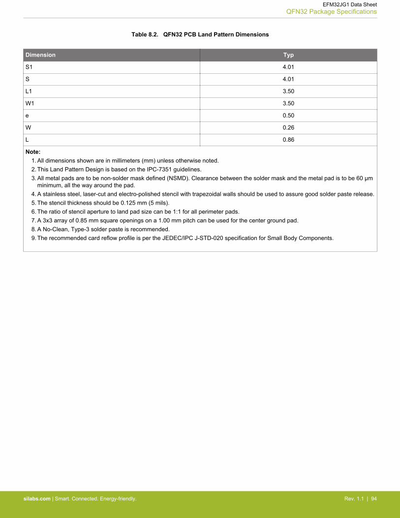
Table 8.2. QFN32 PCB Land Pattern Dimensions
Dimension Typ
S1 4.01
S 4.01
L1 3.50
W1 3.50
e 0.50
W 0.26
L 0.86
Note:1. All dimensions shown are in millimeters (mm) unless otherwise noted.2. This Land Pattern Design is based on the IPC-7351 guidelines.3. All metal pads are to be non-solder mask defined (NSMD). Clearance between the solder mask and the metal pad is to be 60 µm
minimum, all the way around the pad.4. A stainless steel, laser-cut and electro-polished stencil with trapezoidal walls should be used to assure good solder paste release.5. The stencil thickness should be 0.125 mm (5 mils).6. The ratio of stencil aperture to land pad size can be 1:1 for all perimeter pads.7. A 3x3 array of 0.85 mm square openings on a 1.00 mm pitch can be used for the center ground pad.8. A No-Clean, Type-3 solder paste is recommended.9. The recommended card reflow profile is per the JEDEC/IPC J-STD-020 specification for Small Body Components.
EFM32JG1 Data SheetQFN32 Package Specifications
silabs.com | Smart. Connected. Energy-friendly. Rev. 1.1 | 94
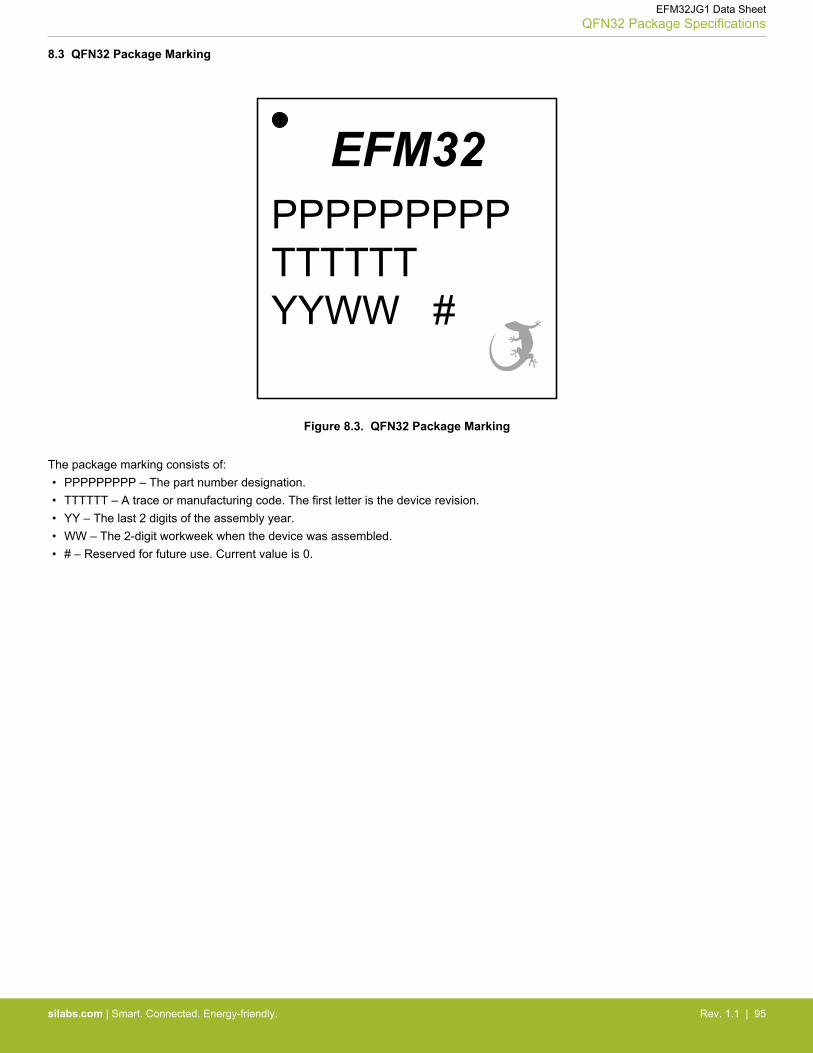
8.3 QFN32 Package Marking
PPPPPPPPPTTTTTTYYWW #
EFM32
Figure 8.3. QFN32 Package Marking
The package marking consists of:• PPPPPPPPP – The part number designation.• TTTTTT – A trace or manufacturing code. The first letter is the device revision.• YY – The last 2 digits of the assembly year.• WW – The 2-digit workweek when the device was assembled.• # – Reserved for future use. Current value is 0.
EFM32JG1 Data SheetQFN32 Package Specifications
silabs.com | Smart. Connected. Energy-friendly. Rev. 1.1 | 95
9. Revision History
9.1 Revision 1.1
2016-Oct-26
• System Overview Sections: Minor wording and typographical error fixes.• Electrical Characteristics: Minor wording and typographical error fixes.• "HFRCO and AUXHFRCO" table in Electrical Characteristics: f_HFRCO symbol changed to f_HFRCO_ACC.• Pinout tables: APORT channel details removed from "Analog" column. This information is now found in the APORT client map sec-
tions.• Updated APORT client map sections.
9.2 Revision 1.0
2016-Jul-22
• Electrical Characteristics: Minimum and maximum value statement changed to cover full operating temperature range.• Finalized Specification Tables. Tables with condition/min/typ/max or footnote changes include:
• Absolute Maximum Ratings• General Operating Conditions• DC-DC Converter• LFRCO• HFRCO and AUXHFRCO• ADC• IDAC
• Updated Typical Performance Graphs.• Added note for 5V tolerance to pinout GPIO Overview sections.• Updated OPN decoder with latest revision.• Updated Package Marking text with latest descriptions.
9.3 Revision 0.95
2016-04-11
• All OPNs changed to rev C0.• Electrical specification tables updated with latest characterization data and production test limits.
9.4 Revision 0.31
• Engineering samples note added to ordering information table.
9.5 Revision 0.3
• Re-formatted ordering information table and OPN decoder.• Removed extraneous sections from dc-dc from system overview.• Updated table formatting for electrical specifications.• Updated electrical specifications with latest available data.• Added I2C and USART SPI timing tables.• Moved dc-dc graph to typical performance curves.• Updated APORT tables and APORT references to correct nomenclature.• Updated top marking description.
9.6 Revision 0.2
Updated ordering table.
Changed "1.62 V to 3.8 V Single Power Supply" to "1.62 V to 3.8 V Power Supply" in the Feature List.
EFM32JG1 Data SheetRevision History
silabs.com | Smart. Connected. Energy-friendly. Rev. 1.1 | 96
9.7 Revision 0.1
Initial release.
EFM32JG1 Data SheetRevision History
silabs.com | Smart. Connected. Energy-friendly. Rev. 1.1 | 97
Table of Contents1. Feature List . . . . . . . . . . . . . . . . . . . . . . . . . . . . . . . . 1
2. Ordering Information . . . . . . . . . . . . . . . . . . . . . . . . . . . . 2
3. System Overview . . . . . . . . . . . . . . . . . . . . . . . . . . . . . . 33.1 Introduction. . . . . . . . . . . . . . . . . . . . . . . . . . . . . . . 3
3.2 Power . . . . . . . . . . . . . . . . . . . . . . . . . . . . . . . . 43.2.1 Energy Management Unit (EMU) . . . . . . . . . . . . . . . . . . . . . . . 43.2.2 DC-DC Converter . . . . . . . . . . . . . . . . . . . . . . . . . . . . 4
3.3 General Purpose Input/Output (GPIO). . . . . . . . . . . . . . . . . . . . . . 4
3.4 Clocking . . . . . . . . . . . . . . . . . . . . . . . . . . . . . . . . 43.4.1 Clock Management Unit (CMU) . . . . . . . . . . . . . . . . . . . . . . . 43.4.2 Internal and External Oscillators . . . . . . . . . . . . . . . . . . . . . . . 4
3.5 Counters/Timers and PWM . . . . . . . . . . . . . . . . . . . . . . . . . 53.5.1 Timer/Counter (TIMER) . . . . . . . . . . . . . . . . . . . . . . . . . . 53.5.2 Real Time Counter and Calendar (RTCC) . . . . . . . . . . . . . . . . . . . . 53.5.3 Low Energy Timer (LETIMER). . . . . . . . . . . . . . . . . . . . . . . . 53.5.4 Ultra Low Power Wake-up Timer (CRYOTIMER) . . . . . . . . . . . . . . . . . 53.5.5 Pulse Counter (PCNT) . . . . . . . . . . . . . . . . . . . . . . . . . . 53.5.6 Watchdog Timer (WDOG) . . . . . . . . . . . . . . . . . . . . . . . . . 5
3.6 Communications and Other Digital Peripherals . . . . . . . . . . . . . . . . . . . 53.6.1 Universal Synchronous/Asynchronous Receiver/Transmitter (USART) . . . . . . . . . . 53.6.2 Low Energy Universal Asynchronous Receiver/Transmitter (LEUART) . . . . . . . . . . 63.6.3 Inter-Integrated Circuit Interface (I2C) . . . . . . . . . . . . . . . . . . . . . 63.6.4 Peripheral Reflex System (PRS) . . . . . . . . . . . . . . . . . . . . . . . 6
3.7 Security Features. . . . . . . . . . . . . . . . . . . . . . . . . . . . . 63.7.1 GPCRC (General Purpose Cyclic Redundancy Check) . . . . . . . . . . . . . . . 63.7.2 Crypto Accelerator (CRYPTO). . . . . . . . . . . . . . . . . . . . . . . . 6
3.8 Analog . . . . . . . . . . . . . . . . . . . . . . . . . . . . . . . . 63.8.1 Analog Port (APORT) . . . . . . . . . . . . . . . . . . . . . . . . . . 63.8.2 Analog Comparator (ACMP) . . . . . . . . . . . . . . . . . . . . . . . . 63.8.3 Analog to Digital Converter (ADC) . . . . . . . . . . . . . . . . . . . . . . 73.8.4 Digital to Analog Current Converter (IDAC) . . . . . . . . . . . . . . . . . . . 7
3.9 Reset Management Unit (RMU) . . . . . . . . . . . . . . . . . . . . . . . . 7
3.10 Core and Memory . . . . . . . . . . . . . . . . . . . . . . . . . . . . 73.10.1 Processor Core . . . . . . . . . . . . . . . . . . . . . . . . . . . . 73.10.2 Memory System Controller (MSC) . . . . . . . . . . . . . . . . . . . . . . 73.10.3 Linked Direct Memory Access Controller (LDMA) . . . . . . . . . . . . . . . . . 7
3.11 Memory Map . . . . . . . . . . . . . . . . . . . . . . . . . . . . . . 8
3.12 Configuration Summary . . . . . . . . . . . . . . . . . . . . . . . . . . 9
4. Electrical Specifications . . . . . . . . . . . . . . . . . . . . . . . . . . 104.1 Electrical Characteristics . . . . . . . . . . . . . . . . . . . . . . . . . .104.1.1 Absolute Maximum Ratings . . . . . . . . . . . . . . . . . . . . . . . .10
Table of Contents 98

4.1.2 Operating Conditions . . . . . . . . . . . . . . . . . . . . . . . . . . .114.1.2.1 General Operating Conditions . . . . . . . . . . . . . . . . . . . . . . .114.1.3 Thermal Characteristics . . . . . . . . . . . . . . . . . . . . . . . . . .124.1.4 DC-DC Converter . . . . . . . . . . . . . . . . . . . . . . . . . . . .134.1.5 Current Consumption. . . . . . . . . . . . . . . . . . . . . . . . . . .154.1.5.1 Current Consumption 3.3 V without DC-DC Converter . . . . . . . . . . . . . . .154.1.5.2 Current Consumption 3.3 V using DC-DC Converter . . . . . . . . . . . . . . .164.1.5.3 Current Consumption 1.85 V without DC-DC Converter . . . . . . . . . . . . . .184.1.6 Wake up times . . . . . . . . . . . . . . . . . . . . . . . . . . . . .194.1.7 Brown Out Detector . . . . . . . . . . . . . . . . . . . . . . . . . . .194.1.8 Oscillators . . . . . . . . . . . . . . . . . . . . . . . . . . . . . .204.1.8.1 LFXO . . . . . . . . . . . . . . . . . . . . . . . . . . . . . . .204.1.8.2 HFXO . . . . . . . . . . . . . . . . . . . . . . . . . . . . . . .214.1.8.3 LFRCO . . . . . . . . . . . . . . . . . . . . . . . . . . . . . . .214.1.8.4 HFRCO and AUXHFRCO . . . . . . . . . . . . . . . . . . . . . . . .224.1.8.5 ULFRCO . . . . . . . . . . . . . . . . . . . . . . . . . . . . . .224.1.9 Flash Memory Characteristics . . . . . . . . . . . . . . . . . . . . . . . .234.1.10 GPIO. . . . . . . . . . . . . . . . . . . . . . . . . . . . . . . .244.1.11 VMON . . . . . . . . . . . . . . . . . . . . . . . . . . . . . . .254.1.12 ADC . . . . . . . . . . . . . . . . . . . . . . . . . . . . . . . .264.1.13 IDAC . . . . . . . . . . . . . . . . . . . . . . . . . . . . . . . .294.1.14 Analog Comparator (ACMP) . . . . . . . . . . . . . . . . . . . . . . . .314.1.15 I2C . . . . . . . . . . . . . . . . . . . . . . . . . . . . . . . .334.1.16 USART SPI . . . . . . . . . . . . . . . . . . . . . . . . . . . . .36
4.2 Typical Performance Curves . . . . . . . . . . . . . . . . . . . . . . . . .374.2.1 Supply Current . . . . . . . . . . . . . . . . . . . . . . . . . . . . .384.2.2 DC-DC Converter . . . . . . . . . . . . . . . . . . . . . . . . . . . .404.2.3 Internal Oscillators. . . . . . . . . . . . . . . . . . . . . . . . . . . .42
5. Typical Connection Diagrams . . . . . . . . . . . . . . . . . . . . . . . . 485.1 Power . . . . . . . . . . . . . . . . . . . . . . . . . . . . . . . .48
5.2 Other Connections . . . . . . . . . . . . . . . . . . . . . . . . . . . .48
6. Pin Definitions . . . . . . . . . . . . . . . . . . . . . . . . . . . . . . 496.1 EFM32JG1 QFN48 with DC-DC Definition . . . . . . . . . . . . . . . . . . . .496.1.1 EFM32JG1 QFN48 with DC-DC GPIO Overview . . . . . . . . . . . . . . . . .59
6.2 EFM32JG1 QFN32 without DC-DC Definition . . . . . . . . . . . . . . . . . . .606.2.1 EFM32JG1 QFN32 without DC-DC GPIO Overview . . . . . . . . . . . . . . . .68
6.3 EFM32JG1 QFN32 with DC-DC Definition . . . . . . . . . . . . . . . . . . . .696.3.1 EFM32JG1 QFN32 with DC-DC GPIO Overview . . . . . . . . . . . . . . . . .76
6.4 Alternate Functionality Pinout . . . . . . . . . . . . . . . . . . . . . . . .77
6.5 Analog Port (APORT) Client Maps . . . . . . . . . . . . . . . . . . . . . . .83
7. QFN48 Package Specifications. . . . . . . . . . . . . . . . . . . . . . . . 867.1 QFN48 Package Dimensions. . . . . . . . . . . . . . . . . . . . . . . . .86
7.2 QFN48 PCB Land Pattern . . . . . . . . . . . . . . . . . . . . . . . . . .88
7.3 QFN48 Package Marking . . . . . . . . . . . . . . . . . . . . . . . . . .90
Table of Contents 99
8. QFN32 Package Specifications. . . . . . . . . . . . . . . . . . . . . . . . 918.1 QFN32 Package Dimensions. . . . . . . . . . . . . . . . . . . . . . . . .91
8.2 QFN32 PCB Land Pattern . . . . . . . . . . . . . . . . . . . . . . . . . .93
8.3 QFN32 Package Marking . . . . . . . . . . . . . . . . . . . . . . . . . .95
9. Revision History . . . . . . . . . . . . . . . . . . . . . . . . . . . . . 969.1 Revision 1.1 . . . . . . . . . . . . . . . . . . . . . . . . . . . . . .96
9.2 Revision 1.0 . . . . . . . . . . . . . . . . . . . . . . . . . . . . . .96
9.3 Revision 0.95 . . . . . . . . . . . . . . . . . . . . . . . . . . . . . .96
9.4 Revision 0.31 . . . . . . . . . . . . . . . . . . . . . . . . . . . . . .96
9.5 Revision 0.3 . . . . . . . . . . . . . . . . . . . . . . . . . . . . . .96
9.6 Revision 0.2 . . . . . . . . . . . . . . . . . . . . . . . . . . . . . .96
9.7 Revision 0.1 . . . . . . . . . . . . . . . . . . . . . . . . . . . . . .97
Table of Contents . . . . . . . . . . . . . . . . . . . . . . . . . . . . . . 98
Table of Contents 100

http://www.silabs.com
Silicon Laboratories Inc.400 West Cesar ChavezAustin, TX 78701USA
Simplicity StudioOne-click access to MCU and wireless tools, documentation, software, source code libraries & more. Available for Windows, Mac and Linux!
IoT Portfoliowww.silabs.com/IoT
SW/HWwww.silabs.com/simplicity
Qualitywww.silabs.com/quality
Support and Communitycommunity.silabs.com
DisclaimerSilicon Labs intends to provide customers with the latest, accurate, and in-depth documentation of all peripherals and modules available for system and software implementers using or intending to use the Silicon Labs products. Characterization data, available modules and peripherals, memory sizes and memory addresses refer to each specific device, and "Typical" parameters provided can and do vary in different applications. Application examples described herein are for illustrative purposes only. Silicon Labs reserves the right to make changes without further notice and limitation to product information, specifications, and descriptions herein, and does not give warranties as to the accuracy or completeness of the included information. Silicon Labs shall have no liability for the consequences of use of the information supplied herein. This document does not imply or express copyright licenses granted hereunder to design or fabricate any integrated circuits. The products are not designed or authorized to be used within any Life Support System without the specific written consent of Silicon Labs. A "Life Support System" is any product or system intended to support or sustain life and/or health, which, if it fails, can be reasonably expected to result in significant personal injury or death. Silicon Labs products are not designed or authorized for military applications. Silicon Labs products shall under no circumstances be used in weapons of mass destruction including (but not limited to) nuclear, biological or chemical weapons, or missiles capable of delivering such weapons.
Trademark InformationSilicon Laboratories Inc.® , Silicon Laboratories®, Silicon Labs®, SiLabs® and the Silicon Labs logo®, Bluegiga®, Bluegiga Logo®, Clockbuilder®, CMEMS®, DSPLL®, EFM®, EFM32®, EFR, Ember®, Energy Micro, Energy Micro logo and combinations thereof, "the world’s most energy friendly microcontrollers", Ember®, EZLink®, EZRadio®, EZRadioPRO®, Gecko®, ISOmodem®, Precision32®, ProSLIC®, Simplicity Studio®, SiPHY®, Telegesis, the Telegesis Logo®, USBXpress® and others are trademarks or registered trademarks of Silicon Labs. ARM, CORTEX, Cortex-M3 and THUMB are trademarks or registered trademarks of ARM Holdings. Keil is a registered trademark of ARM Limited. All other products or brand names mentioned herein are trademarks of their respective holders.
Top Related