


Languages
Pages
Legal

Effect of Particle Size on the Adsorption and
Desorption Properties of Oxide Nanoparticles
Task 425.023
SRC/SEMATECH Engineering Research Center for Environmentally Benign Semiconductor Manufacturing
PIs:
Farhang Shadman
Dept. Chemical & Environmental Engineering, University of Arizona.
Reyes Sierra
Dept. Chemical & Environmental Engineering, University of Arizona.
Buddy Ratner
University of Washington Engineered Biomaterials (UWEB) Center, University of Washington
Hao Wang
Chemical and Environmental Engineering
University of Arizona
April 19th, 2012
SRC/SEMATECH Engineering Research Center for Environmentally Benign Semiconductor Manufacturing 2
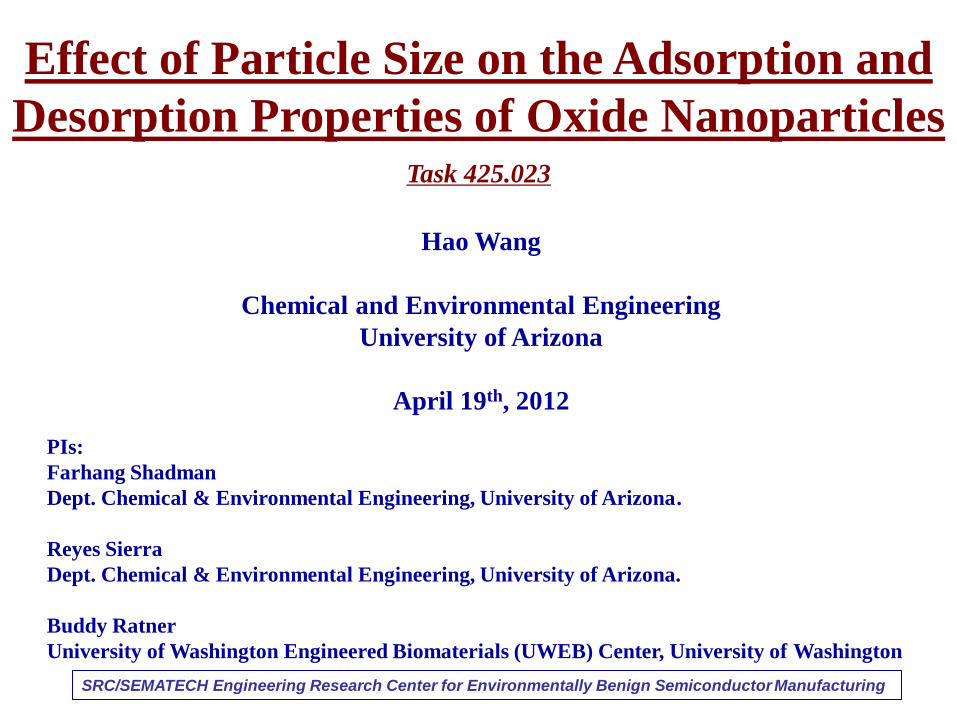
ESH Testing and Evaluation of NPs
Handy, R.D., Shaw, B.J., 2007. Toxic effects of nanoparticles and nanomaterials: Implications for public health, risk
assessment and the public perception of nanotechnology. Health Risk Society 9, 125-144.
Surface Properties: capacity, affinity, and activation energy
0
10
20
30
40
50
60
70
80
90
100
0 50 100 150 200
Mois
ture
Rete
nti
on
(%
)
Time, t (min)
CeO2, 20nm
HfO2, 20nm SiO2, 20nm
0
10
20
30
40
50
60
70
80
90
100
0 50 100 150 200
Mois
ture
Rete
nti
on
(%
)
Time, t (min)
HfO2, 20nm
HfO2, 100nm
SRC/SEMATECH Engineering Research Center for Environmentally Benign Semiconductor Manufacturing 3
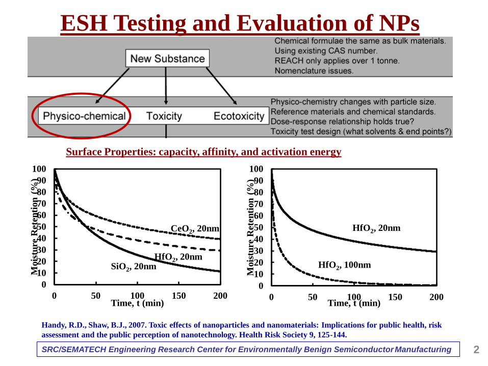
Objectives and Method Approach
Objective: Characterization of the surface sites on nanoparticles that
contribute to concentration, retention, and enhanced transport of toxic
chemicals.
Method approach: Surface hydroxylation (adsorption and desorption
of contaminants).
Results: Capacity and
energetics of capture and
retention of contaminants
on active sites.
Materials: SiO2, HfO2, and
CeO2.
Parameters: Oxide type,
particle size, temperature.
SRC/SEMATECH Engineering Research Center for Environmentally Benign Semiconductor Manufacturing 4
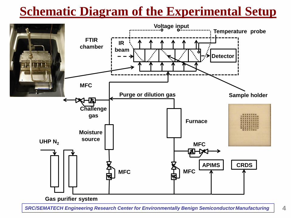
Schematic Diagram of the Experimental Setup
APIMS CRDS
MFC
Gas purifier system
UHP N2 MFC
MFC
MFC
Moisture
source
Furnace
FTIR
chamber
IR
beam
Detector
Sample holder
Challenge
gas
Purge or dilution gas
Voltage input Temperature probe
SRC/SEMATECH Engineering Research Center for Environmentally Benign Semiconductor Manufacturing
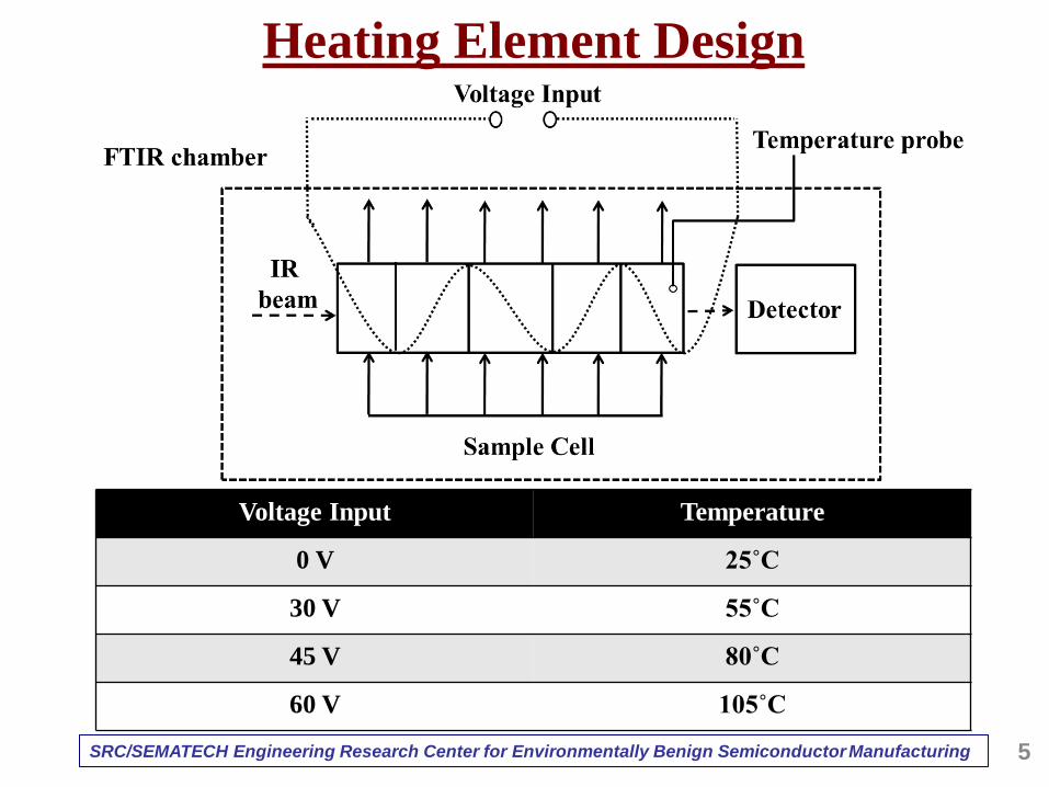
Heating Element Design
Voltage Input Temperature
0 V 25˚C
30 V 55˚C
45 V 80˚C
60 V 105˚C
5
SRC/SEMATECH Engineering Research Center for Environmentally Benign Semiconductor Manufacturing
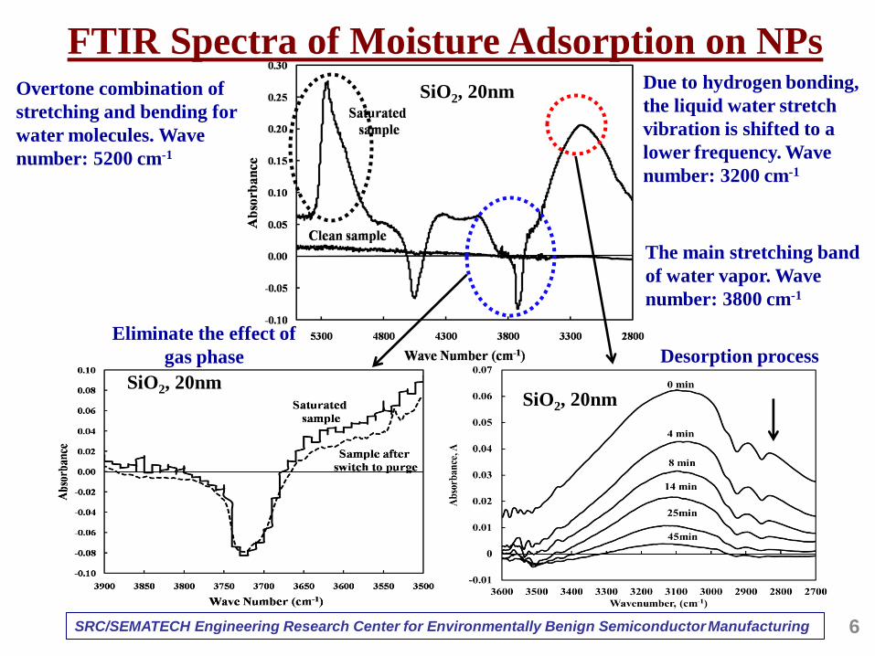
FTIR Spectra of Moisture Adsorption on NPs Due to hydrogen bonding,
the liquid water stretch
vibration is shifted to a
lower frequency. Wave
number: 3200 cm-1
Overtone combination of
stretching and bending for
water molecules. Wave
number: 5200 cm-1
Desorption process
Eliminate the effect of
gas phase
SiO2, 20nm
SiO2, 20nm
SiO2, 20nm
6
The main stretching band
of water vapor. Wave
number: 3800 cm-1
SRC/SEMATECH Engineering Research Center for Environmentally Benign Semiconductor Manufacturing
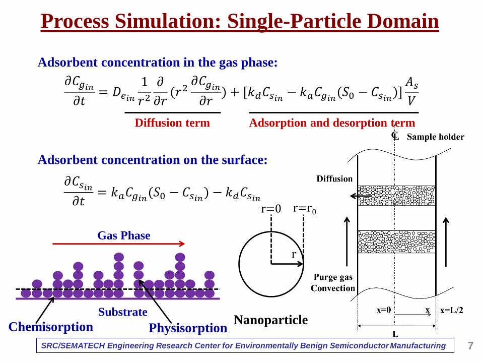
Process Simulation: Single-Particle Domain
Adsorbent concentration in the gas phase:
Adsorbent concentration on the surface:
r=0 r=r0
Nanoparticle
r
Diffusion term Adsorption and desorption term
7
Substrate
Gas Phase
𝜕𝐶𝑔𝑖𝑛𝜕𝑡
= 𝐷𝑒𝑖𝑛1
𝑟2𝜕
𝜕𝑟(𝑟2𝜕𝐶𝑔𝑖𝑛𝜕𝑟
) + [𝑘𝑑𝐶𝑠𝑖𝑛 − 𝑘𝑎𝐶𝑔𝑖𝑛(𝑆0 − 𝐶𝑠𝑖𝑛)]𝐴𝑠𝑉
𝜕𝐶𝑠𝑖𝑛𝜕𝑡
= 𝑘𝑎𝐶𝑔𝑖𝑛(𝑆0 − 𝐶𝑠𝑖𝑛) − 𝑘𝑑𝐶𝑠𝑖𝑛
Chemisorption Physisorption
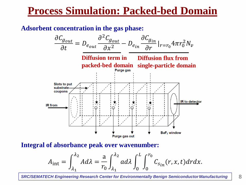
SRC/SEMATECH Engineering Research Center for Environmentally Benign Semiconductor Manufacturing 8
Adsorbent concentration in the gas phase:
Process Simulation: Packed-bed Domain
Diffusion term in
packed-bed domain
Diffusion flux from
single-particle domain
𝜕𝐶𝑔𝑜𝑢𝑡𝜕𝑡
= 𝐷𝑒𝑜𝑢𝑡𝜕2𝐶𝑔𝑜𝑢𝑡𝜕𝑥2
− 𝐷𝑒𝑖𝑛𝜕𝐶𝑔𝑖𝑛𝜕𝑟
|𝑟=𝑟04𝜋𝑟02𝑁𝑣
𝐴int = 𝜆2
𝜆1
𝐴𝑑𝜆 =a
𝑟0 𝜆2
𝜆1
𝑎𝑑𝜆 𝐿
0
𝑟0
0
𝐶𝑠𝑖𝑛(𝑟, 𝑥, 𝑡)𝑑𝑟𝑑𝑥.
Integral of absorbance peak over wavenumber:
SRC/SEMATECH Engineering Research Center for Environmentally Benign Semiconductor Manufacturing
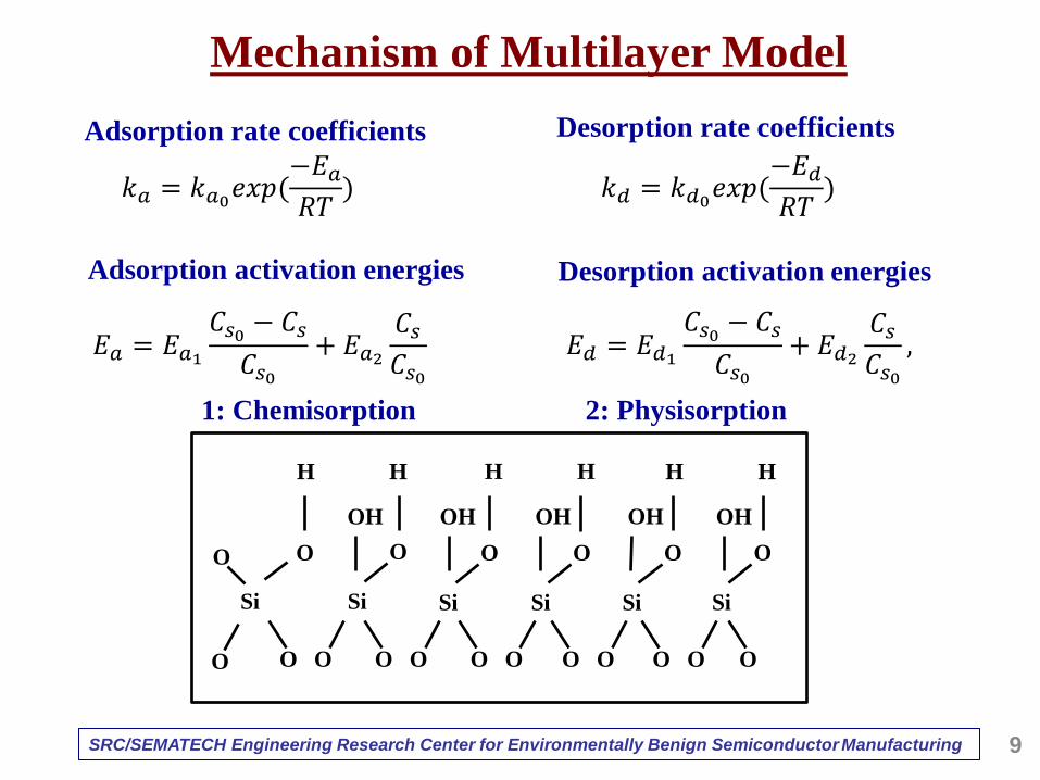
Si
O
Si
O
Si
O
Si
O
Si
O
Si
O
H H H H H H
OH OH OH OH OH
O O O O O O O O O O O O
O
𝑘𝑎 = 𝑘𝑎0𝑒𝑥𝑝(−𝐸𝑎𝑅𝑇) 𝑘𝑑 = 𝑘𝑑0𝑒𝑥𝑝(
−𝐸𝑑𝑅𝑇)
𝐸𝑎 = 𝐸𝑎1𝐶𝑠0 − 𝐶𝑠
𝐶𝑠0+ 𝐸𝑎2
𝐶𝑠𝐶𝑠0
𝐸𝑑 = 𝐸𝑑1𝐶𝑠0 − 𝐶𝑠
𝐶𝑠0+ 𝐸𝑑2
𝐶𝑠𝐶𝑠0,
Adsorption rate coefficients Desorption rate coefficients
Desorption activation energies Adsorption activation energies
Mechanism of Multilayer Model
1: Chemisorption 2: Physisorption
9
SRC/SEMATECH Engineering Research Center for Environmentally Benign Semiconductor Manufacturing
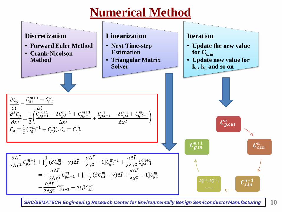
Numerical Method
𝑪𝒈,𝒐𝒖𝒕𝒏
𝑪𝒔,𝒊𝒏𝒏
𝑪𝒔,𝒊𝒏𝒏+𝟏 𝒌𝒂
𝒏+𝟏, 𝒌𝒅𝒏+𝟏,
……
𝑪𝒈,𝒊𝒏𝒏+𝟏
𝜕𝐶𝑔
𝜕𝑡=𝐶𝑔,𝑖𝑚+1 − 𝐶𝑔,𝑖
𝑚
𝛥𝑡
𝜕2𝐶𝑔
𝜕𝑥2=1
2
𝐶𝑔,𝑖+1𝑚+1 − 2𝐶𝑔,𝑖
𝑚+1 + 𝐶𝑔,𝑖−1𝑚+1
Δ𝑥2+𝐶𝑔,𝑖+1𝑚 − 2𝐶𝑔,𝑖
𝑚 + 𝐶𝑔,𝑖−1𝑚
Δ𝑥2
𝐶𝑔 =1
2(𝐶𝑔,𝑖𝑚+1 + 𝐶𝑔,𝑖
𝑚), 𝐶𝑠 = 𝐶𝑠,𝑖𝑚.
𝛼Δ𝑡
2Δ𝑥 2𝐶 𝑔,𝑖+1𝑚+1 + [
1
2(𝛿𝐶 𝑠,𝑖
𝑚 − 𝛾)Δ𝑡 −𝛼Δ𝑡
Δ𝑥 2− 1]𝐶 𝑔,𝑖
𝑚+1 +𝛼Δ𝑡
2Δ𝑥 2𝐶 𝑔,𝑖−1𝑚+1
= −𝛼Δ𝑡
2Δ𝑥 2𝐶 𝑔,𝑖+1𝑚 + [−
1
2(𝛿𝐶 𝑠,𝑖
𝑚 − 𝛾)Δ𝑡 +𝛼Δ𝑡
Δ𝑥 2− 1]𝐶 𝑔,𝑖
𝑚
−𝛼Δ𝑡
2Δ𝑥 2𝐶 𝑔,𝑖−1𝑚 − Δ𝑡 𝛽𝐶 𝑠,𝑖
𝑚
Discretization
• Forward Euler Method
• Crank-Nicolson Method
Linearization
• Next Time-step Estimation
• Triangular Matrix Solver
Iteration
• Update the new value for Cs, in
• Update new value for ka, kd and so on
10
SRC/SEMATECH Engineering Research Center for Environmentally Benign Semiconductor Manufacturing
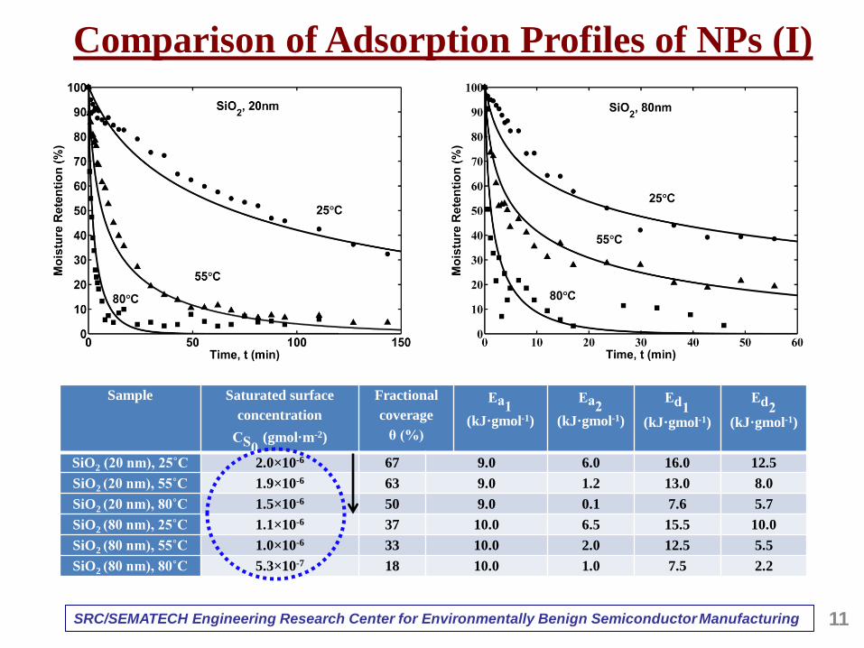
Comparison of Adsorption Profiles of NPs (I)
11
Sample
Saturated surface
concentration
CS0 (gmol·m-2)
Fractional
coverage
θ (%)
Ea1
(kJ·gmol-1)
Ea2
(kJ·gmol-1)
Ed1
(kJ·gmol-1)
Ed2
(kJ·gmol-1)
SiO2 (20 nm), 25˚C 2.0×10⁻⁶ 67 9.0 6.0 16.0 12.5
SiO2 (20 nm), 55˚C 1.9×10⁻⁶ 63 9.0 1.2 13.0 8.0
SiO2 (20 nm), 80˚C 1.5×10⁻⁶ 50 9.0 0.1 7.6 5.7
SiO2 (80 nm), 25˚C 1.1×10⁻⁶ 37 10.0 6.5 15.5 10.0
SiO2 (80 nm), 55˚C 1.0×10⁻⁶ 33 10.0 2.0 12.5 5.5
SiO2 (80 nm), 80˚C 5.3×10⁻⁷ 18 10.0 1.0 7.5 2.2
SRC/SEMATECH Engineering Research Center for Environmentally Benign Semiconductor Manufacturing 12
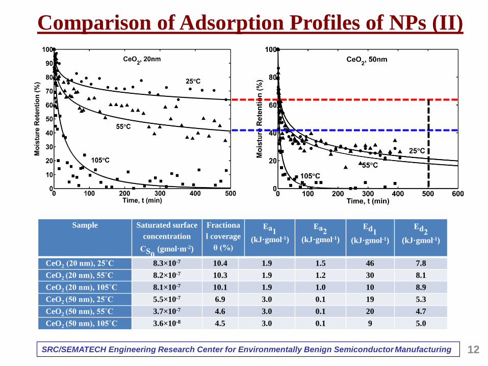
Comparison of Adsorption Profiles of NPs (II)
Sample
Saturated surface
concentration
CS0 (gmol·m-2)
Fractiona
l coverage
θ (%)
Ea1
(kJ·gmol-1)
Ea2
(kJ·gmol-1)
Ed1
(kJ·gmol-1)
Ed2
(kJ·gmol-1)
CeO2 (20 nm), 25˚C 8.3×10⁻⁷ 10.4 1.9 1.5 46 7.8
CeO2 (20 nm), 55˚C 8.2×10⁻⁷ 10.3 1.9 1.2 30 8.1
CeO2 (20 nm), 105˚C 8.1×10⁻⁷ 10.1 1.9 1.0 10 8.9
CeO2 (50 nm), 25˚C 5.5×10⁻⁷ 6.9 3.0 0.1 19 5.3
CeO2 (50 nm), 55˚C 3.7×10⁻⁷ 4.6 3.0 0.1 20 4.7
CeO2 (50 nm), 105˚C 3.6×10⁻⁸ 4.5 3.0 0.1 9 5.0

SRC/SEMATECH Engineering Research Center for Environmentally Benign Semiconductor Manufacturing
Comparison of Adsorption Profiles of NPs (III)
13
Sample
Saturated surface
concentration
CS0 (gmol·m-2)
Fractional
coverage
θ (%)
Ea1
(kJ·gmol-1)
Ea2
(kJ·gmol-1)
Ed1
(kJ·gmol-1)
Ed2
(kJ·gmol-1)
HfO2 (20 nm), 25˚C 2.2×10⁻⁶ 55 5.0 0.5 17.0 0.4
HfO2 (20 nm), 55˚C 1.5×10⁻⁶ 38 5.0 2.8 23.5 0.7
HfO2 (20 nm), 80˚C 8.1×10⁻⁷ 20 5.0 4.8 22.0 0.016
HfO2 (100 nm), 25˚C 4.4×10⁻⁷ 11 12.5 10.5 16.5 4.6
HfO2 (100 nm), 55˚C 3.3×10⁻⁷ 8.3 12.5 11.0 16.0 3.7
HfO2 (100 nm), 80˚C 3.1×10⁻⁷ 7.8 12.5 12.0 11.0 2.6
SRC/SEMATECH Engineering Research Center for Environmentally Benign Semiconductor Manufacturing
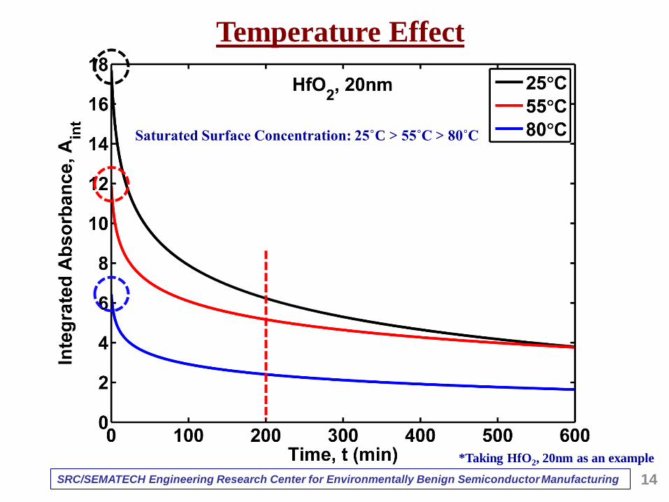
Temperature Effect
*Taking HfO2, 20nm as an example
14
Saturated Surface Concentration: 25˚C > 55˚C > 80˚C
SRC/SEMATECH Engineering Research Center for Environmentally Benign Semiconductor Manufacturing 15
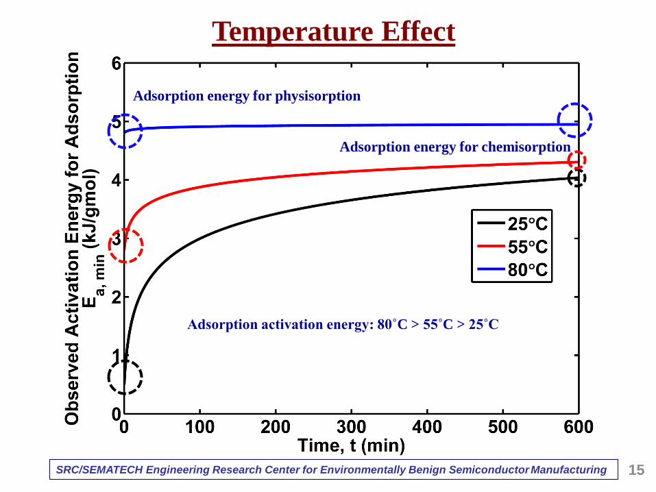
Adsorption activation energy: 80˚C > 55˚C > 25˚C
Temperature Effect
Adsorption energy for physisorption
Adsorption energy for chemisorption
SRC/SEMATECH Engineering Research Center for Environmentally Benign Semiconductor Manufacturing 16
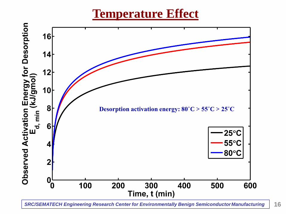
Desorption activation energy: 80˚C > 55˚C > 25˚C
Temperature Effect
SRC/SEMATECH Engineering Research Center for Environmentally Benign Semiconductor Manufacturing
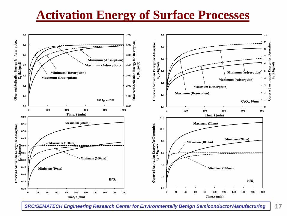
Activation Energy of Surface Processes
17
SRC/SEMATECH Engineering Research Center for Environmentally Benign Semiconductor Manufacturing
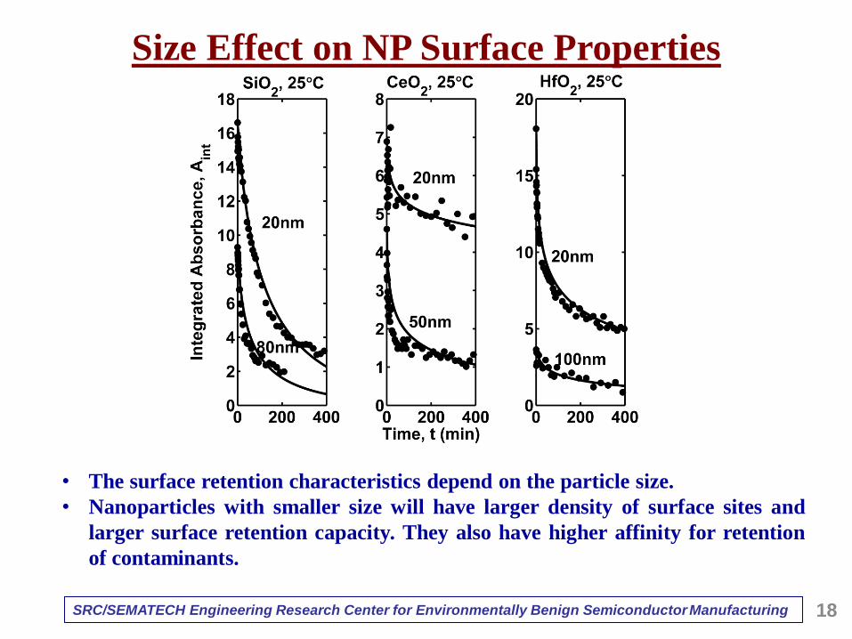
Size Effect on NP Surface Properties
• The surface retention characteristics depend on the particle size.
• Nanoparticles with smaller size will have larger density of surface sites and
larger surface retention capacity. They also have higher affinity for retention
of contaminants.
18
SRC/SEMATECH Engineering Research Center for Environmentally Benign Semiconductor Manufacturing
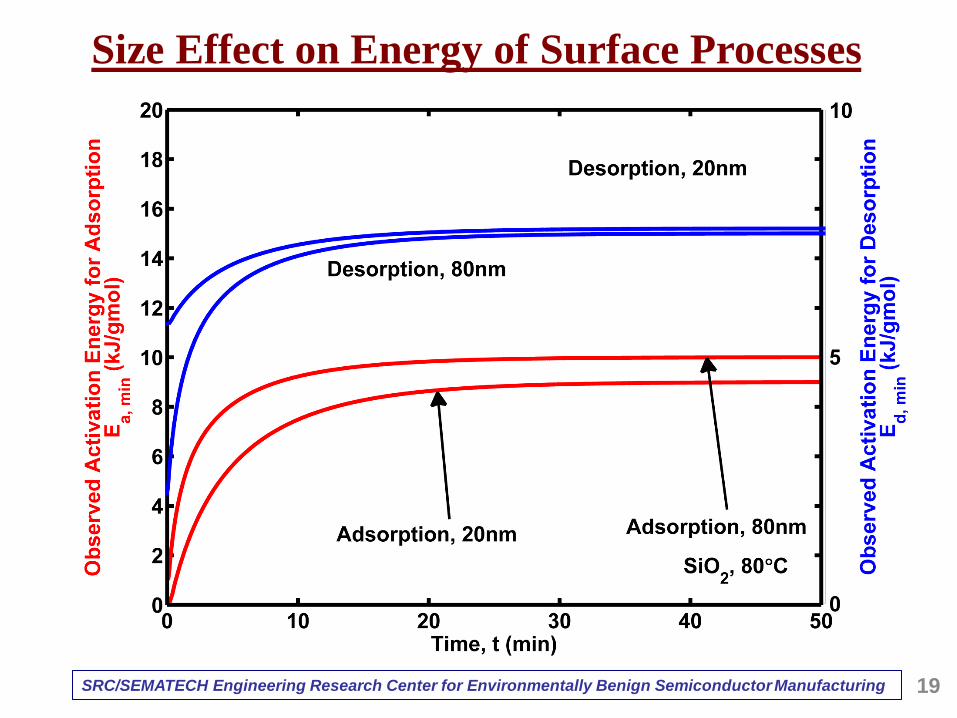
Size Effect on Energy of Surface Processes
19
SRC/SEMATECH Engineering Research Center for Environmentally Benign Semiconductor Manufacturing 20
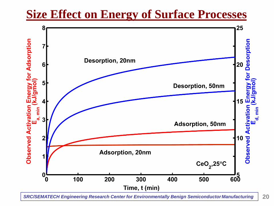
Size Effect on Energy of Surface Processes
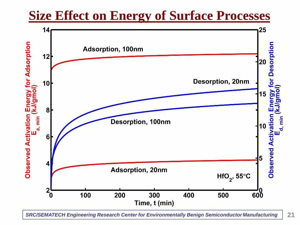
SRC/SEMATECH Engineering Research Center for Environmentally Benign Semiconductor Manufacturing 21
Size Effect on Energy of Surface Processes
SRC/SEMATECH Engineering Research Center for Environmentally Benign Semiconductor Manufacturing 22
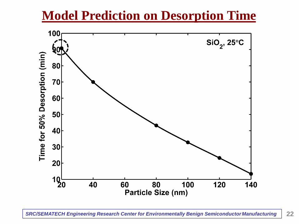
Model Prediction on Desorption Time

SRC/SEMATECH Engineering Research Center for Environmentally Benign Semiconductor Manufacturing 23
Model Prediction on Desorption Time
SRC/SEMATECH Engineering Research Center for Environmentally Benign Semiconductor Manufacturing 24
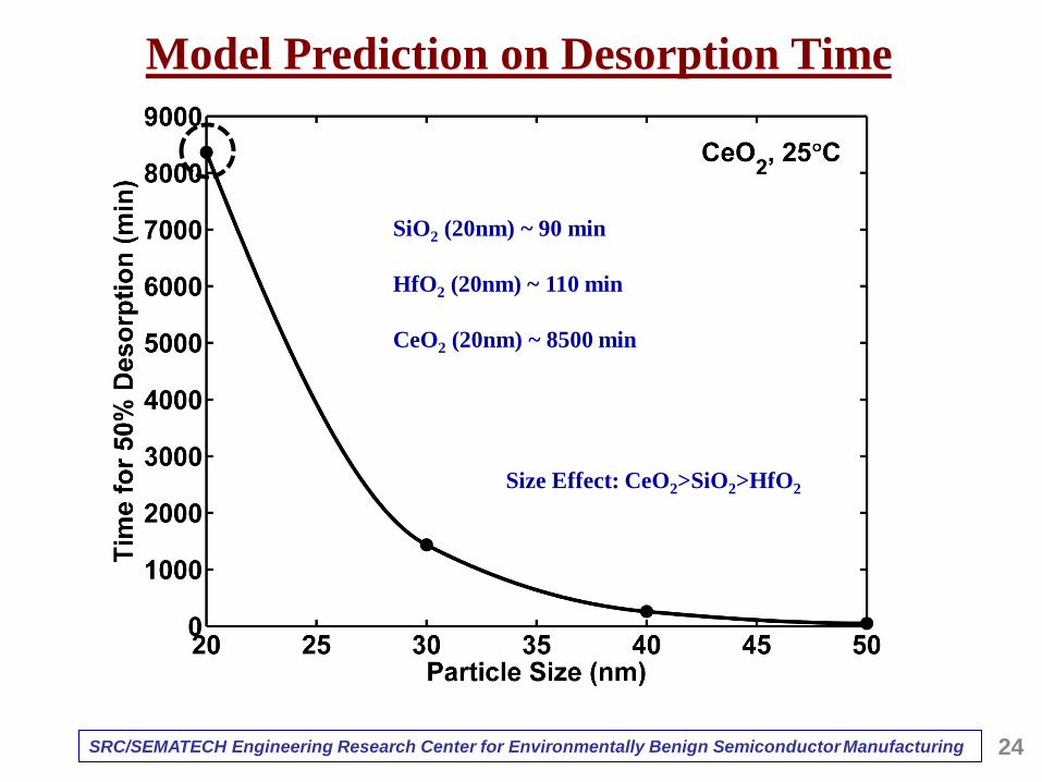
Model Prediction on Desorption Time
SiO2 (20nm) ~ 90 min
HfO2 (20nm) ~ 110 min
CeO2 (20nm) ~ 8500 min
Size Effect: CeO2>SiO2>HfO2
SRC/SEMATECH Engineering Research Center for Environmentally Benign Semiconductor Manufacturing 25
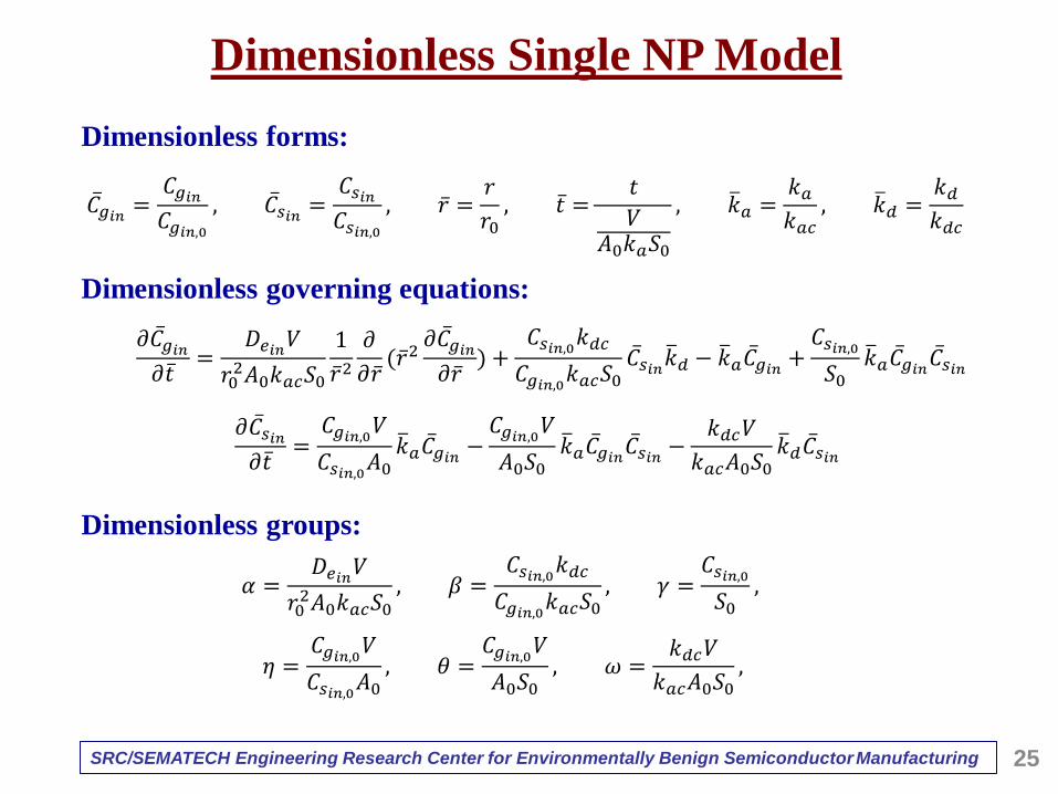
Dimensionless Single NP Model
𝐶 𝑔𝑖𝑛 =𝐶𝑔𝑖𝑛𝐶𝑔𝑖𝑛,0
, 𝐶 𝑠𝑖𝑛 =𝐶𝑠𝑖𝑛𝐶𝑠𝑖𝑛,0
, 𝑟 =𝑟
𝑟0, 𝑡 =
𝑡
𝑉𝐴0𝑘𝑎𝑆0
, 𝑘 𝑎 =𝑘𝑎𝑘𝑎𝑐, 𝑘 𝑑 =
𝑘𝑑𝑘𝑑𝑐
Dimensionless forms:
𝜕𝐶 𝑔𝑖𝑛𝜕𝑡
=𝐷𝑒𝑖𝑛𝑉
𝑟02𝐴0𝑘𝑎𝑐𝑆0
1
𝑟 2𝜕
𝜕𝑟 (𝑟 2𝜕𝐶 𝑔𝑖𝑛𝜕𝑟
) +𝐶𝑠𝑖𝑛,0𝑘𝑑𝑐
𝐶𝑔𝑖𝑛,0𝑘𝑎𝑐𝑆0𝐶 𝑠𝑖𝑛𝑘
𝑑 − 𝑘 𝑎𝐶 𝑔𝑖𝑛 +
𝐶𝑠𝑖𝑛,0𝑆0
𝑘 𝑎𝐶 𝑔𝑖𝑛𝐶 𝑠𝑖𝑛
𝜕𝐶 𝑠𝑖𝑛𝜕𝑡
=𝐶𝑔𝑖𝑛,0𝑉
𝐶𝑠𝑖𝑛,0𝐴0𝑘 𝑎𝐶 𝑔𝑖𝑛 −
𝐶𝑔𝑖𝑛,0𝑉
𝐴0𝑆0𝑘 𝑎𝐶 𝑔𝑖𝑛𝐶
𝑠𝑖𝑛 −
𝑘𝑑𝑐𝑉
𝑘𝑎𝑐𝐴0𝑆0𝑘 𝑑𝐶 𝑠𝑖𝑛
𝛼 =𝐷𝑒𝑖𝑛𝑉
𝑟02𝐴0𝑘𝑎𝑐𝑆0
, 𝛽 =𝐶𝑠𝑖𝑛,0𝑘𝑑𝑐
𝐶𝑔𝑖𝑛,0𝑘𝑎𝑐𝑆0, 𝛾 =
𝐶𝑠𝑖𝑛,0𝑆0
,
𝜂 =𝐶𝑔𝑖𝑛,0𝑉
𝐶𝑠𝑖𝑛,0𝐴0, 𝜃 =
𝐶𝑔𝑖𝑛,0𝑉
𝐴0𝑆0, 𝜔 =
𝑘𝑑𝑐𝑉
𝑘𝑎𝑐𝐴0𝑆0,
Dimensionless governing equations:
Dimensionless groups:
SRC/SEMATECH Engineering Research Center for Environmentally Benign Semiconductor Manufacturing 26
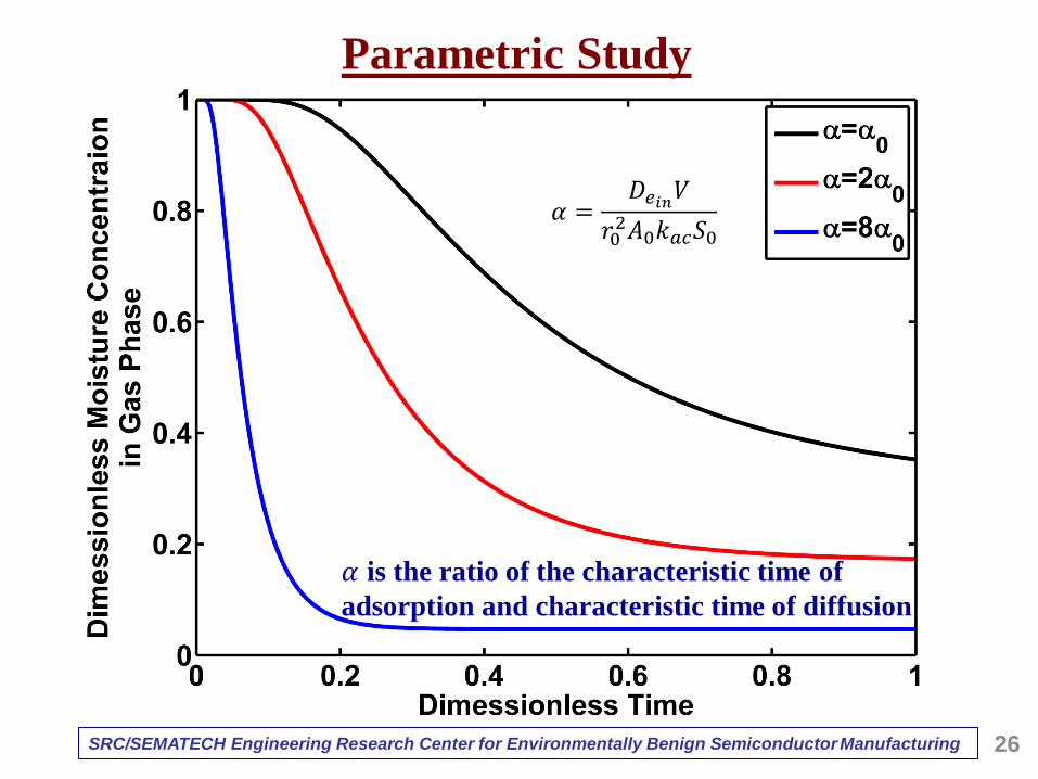
Parametric Study
𝛼 =𝐷𝑒𝑖𝑛𝑉
𝑟02𝐴0𝑘𝑎𝑐𝑆0
𝛼 is the ratio of the characteristic time of
adsorption and characteristic time of diffusion
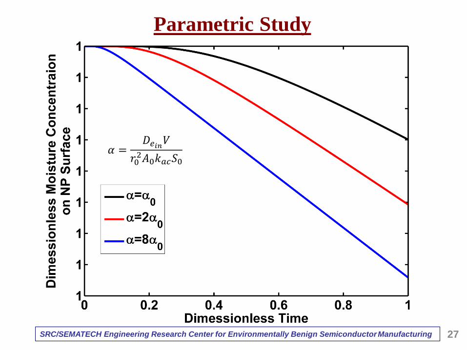
SRC/SEMATECH Engineering Research Center for Environmentally Benign Semiconductor Manufacturing 27
Parametric Study
𝛼 =𝐷𝑒𝑖𝑛𝑉
𝑟02𝐴0𝑘𝑎𝑐𝑆0
SRC/SEMATECH Engineering Research Center for Environmentally Benign Semiconductor Manufacturing
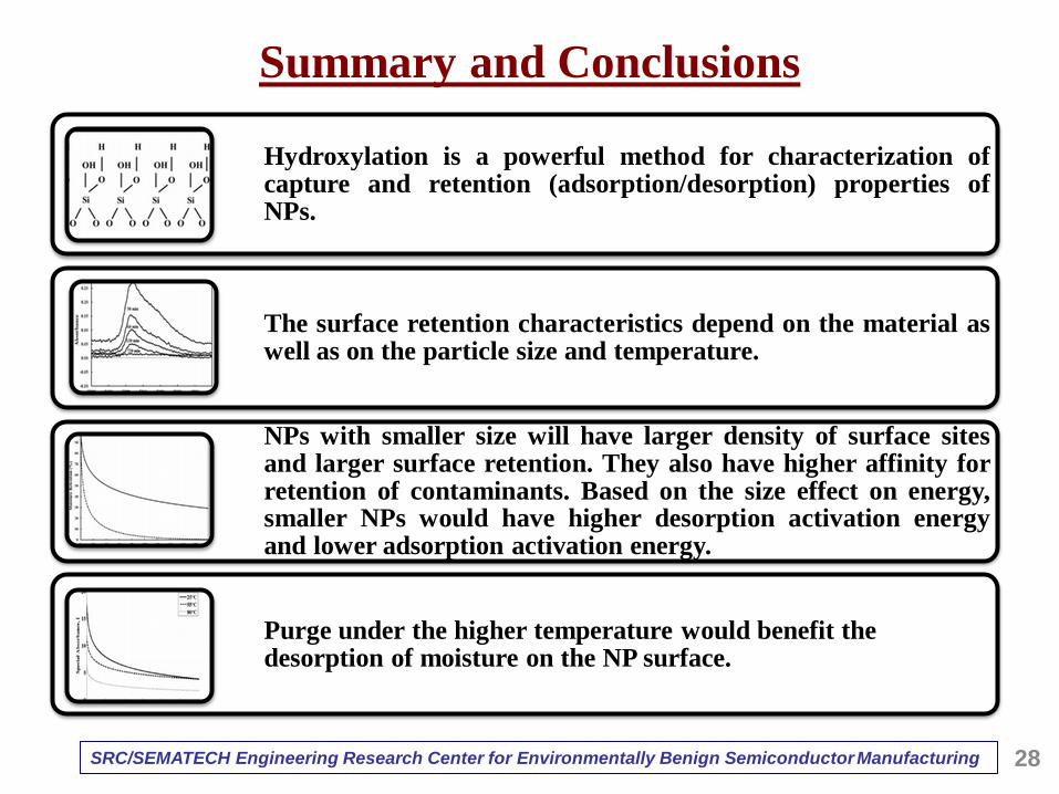
Summary and Conclusions
Hydroxylation is a powerful method for characterization of capture and retention (adsorption/desorption) properties of NPs.
The surface retention characteristics depend on the material as well as on the particle size and temperature.
NPs with smaller size will have larger density of surface sites and larger surface retention. They also have higher affinity for retention of contaminants. Based on the size effect on energy, smaller NPs would have higher desorption activation energy and lower adsorption activation energy.
Purge under the higher temperature would benefit the desorption of moisture on the NP surface.
28
SRC/SEMATECH Engineering Research Center for Environmentally Benign Semiconductor Manufacturing
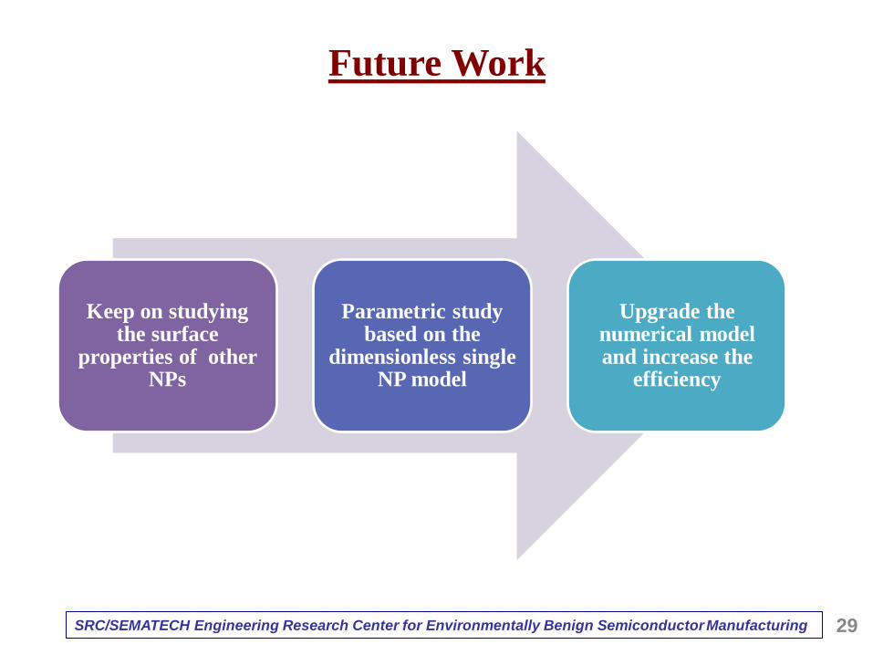
Future Work
Keep on studying the surface
properties of other NPs
Parametric study based on the
dimensionless single NP model
Upgrade the numerical model and increase the
efficiency
29
Publications and Presentations • Hao Wang, F. Shadman, Effect of Particle Size on the Adsorption and Desorption
Properties of Oxide Nanoparticles, Submitted to AIChE, April, 2012
• Hao Wang, J. Yao, F. Shadman, Characterization of the Surface Properties of
Nanoparticles Using Moisture Adsorption Dynamic Profiling, Chemical
Engineering Science, June 2011
• Hao Wang, Characterization of the Surface Properties of Nanoparticles Using
Moisture Adsorption Dynamic Profiling, SRC/SEMATECH Teleconference, July
2011 [PRESENTATION]
• Hao Wang, Physicochemical and Surface Characteristics Study of Nanoparticles
related to ESH Impact of Emerging Nanoparticles and Byproduct in Semiconductor
Manufacturing, SRC/SEMATECH Teleconference, November 2010
[PRESENTATION]
SRC/SEMATECH Engineering Research Center for Environmentally Benign Semiconductor Manufacturing 30
Acknowledgment
• SRC/SEMATECH Engineering Research Center
• Farhang Shadman, Professor of Chemical and Environmental Engineering, UA.
• Reyes Sierra, Professor of Chemical &Environmental Engineering, UA.
• Buddy Ratner, Professor of Bioengineering, UW.
• Junpin Yao, Matheson Tri-Gas Inc.
30
Top Related