


Languages
Pages
Legal


1
EE241 - Spring 2013Advanced Digital Integrated Circuits
Lecture 20: Power gating and body bias
2
Announcements
Homework 4 due next week
Quiz #4 next Monday

2
3
Outline
Last lectureDVS
Clock gating
Managing leakage
This lecturePower gating
Body bias
5. Low Power DesignJ. Power Gating

3
5
Power /Energy Optimization SpaceConstant Throughput/Latency Variable Throughput/Latency
Energy Design Time Sleep Mode Run Time
Active
Logic design
Scaled VDD
Trans. sizing
Multi-VDD
Clock gatingDFS, DVS
Leakage
Stack effects
Trans sizing
Scaling VDD
+ Multi-VTh
Sleep T’s
Multi-VDD
Variable VTh
+ Input control
+ Variable VTh
6
Dynamic Sleep Transistor
ON: gateoverdrive
...
VCC
Virtual VCC
VSS
Virtual VSS
ON: gateoverdrive
Active mode
Noise on virtual supply
PMOS forward body bias
Dual-VT
core
Courtesy of J. Tschanz, Intel (ISSCC’03)

4
7
Dynamic Sleep Transistor
...
VCC
Virtual VCC
VSS
Virtual VSS
OFF: gateunderdrive
OFF: gateunderdrive
Virtual supply collapse
PMOS reverse body biasIdle mode
Courtesy of J. Tschanz, Intel (ISSCC’03)
8
How to Size the Sleep Transistor?
Don’t need both header and footerCircuits in active mode see the sleep transistor as extra power line resistance
The wider the sleep transistor, the better
Wide sleep transistors cost areaMinimize the size of the sleep transistor for given ripple (e.g. 5%)
Need to find the worst case vectorSleep transistor is not for free – it will degrade the performance in active modeCharging and discharging the virtual rails costs energyNeed to sequentially wake up

5
9
Sleep Transistor
High-VTH transistor has to be very large for low resistancein linear region. Low-VTH transistor needs much less areafor the same resistance.
Courtesy: R. Krishnamurthy, Intel
10
Sleep Transistor Layout
Sleep transistor
cells
ALU
Area overhead
PMOS 6%
NMOS 3%
Tschanz, ISSCC’03

6
11
Sleep in Standard Cells
Uvieghara, ISSCC’04
12
Sleep Transistor Grid
Virtual VCC Virtual VSS
VCC
VSS
M4
M4
VCC
VSS
M4
M4
M3 M3 M3 M3
No sleep transistor PMOS & NMOSsleep transistors
Tschanz, ISSCC’03

7
13
Preserving State
Virtual supply collapse in sleep mode will cause the loss of state in registers
Putting the registers at nominal VDD would preserve the state
These registers leak
The second supply needs to be routed as well
Can lower VDD in sleepSome impact on robustness, noise and SEU immunity
State preservation and recovery
14
SLEEP High VT
SLEEP High VT
CLK
SLEEP High VT
SLEEP High VT
[Mutoh95]
Register Design

8
5. Low Power DesignK. Voltage Scaling in Sleep
16
Power /Energy Optimization SpaceConstant Throughput/Latency Variable Throughput/Latency
Energy Design Time Sleep Mode Run Time
Active
Logic design
Scaled VDD
Trans. sizing
Multi-VDD
Clock gatingDFS, DVS
Leakage
Stack effects
Trans sizing
Scaling VDD
+ Multi-VTh
Sleep T’s
Multi-VDDVariable VTh
+ Input control
+ Variable VTh

9
17
Leakage vs. Supply
0
0.1
0.2
0.3
0.4
0.5
0.6
0.7
0.8
0.9
1
0.2 0.3 0.4 0.5 0.6 0.7 0.8 0.9 1
V DD [V]
Del
ay
(nor
mal
ized
)
0
10
20
30
40
50
60
En
erg
y (n
orm
aliz
ed)
Switching power
Leakage power
Delay
3-10x
5. Low Power DesignL. Multiple Thresholds

10
19
Power /Energy Optimization SpaceConstant Throughput/Latency Variable Throughput/Latency
Energy Design Time Sleep Mode Run Time
Active
Logic design
Scaled VDD
Trans. sizing
Multi-VDD
Clock gatingDFS, DVS
Leakage
Stack effects
Trans sizing
Scaling VDD
+ Multi-VTh
Sleep T’s
Multi-VDD
Variable VTh
+ Input control
+ Variable VTh
20
Technology Options
180 130 90 65 45
Technology [nm]
Ion, HS, LP
Ioff,HP
Ioff,LP
Ig,LP
Ig,HP
HP
LP (LOP)

11
21
Using Multiple Thresholds
Yano, SSTCW’00
5. Low Power DesignL. Transistor Sizing

12
23
Power /Energy Optimization SpaceConstant Throughput/Latency Variable Throughput/Latency
Energy Design Time Sleep Mode Run Time
Active
Logic design
Scaled VDD
Trans. sizing
Multi-VDD
Clock gatingDFS, DVS
Leakage
Stack effects
Trans sizing
Scaling VDD
+ Multi-VTh
Sleep T’s
Multi-VDD
Variable VTh
+ Input control
+ Variable VTh
24
Longer Channels
0
1
2
3
4
5
6
7
8
0.1 0.15 0.2 0.25 0.3
Gate Length [um]
Lea
kag
e C
urr
ent
[nA
]
Switching energy
Leakage Current35%
10%
Lnom
•10% longer gates reduce leakage by 35%• Increases switching energy by 21% with W/L = const.
•Attractive when don’t have to increase W (memory)•Doubling L reduces leakage by 3x (in 0.13um)•Much stronger effect in 28nm!•Effect improves with more aggressive devices
W/L = const.

13
5. Low Power DesignM. Multiple Supplies
26
Power /Energy Optimization SpaceConstant Throughput/Latency Variable Throughput/Latency
Energy Design Time Sleep Mode Run Time
Active
Logic design
Scaled VDD
Trans. sizing
Multi-VDD
Clock gatingDFS, DVS
Leakage
Stack effects
Trans sizing
Scaling VDD
+ Multi-VTh
Sleep T’s
Multi-VDDVariable VTh
+ Input control
+ Variable VTh
14
27
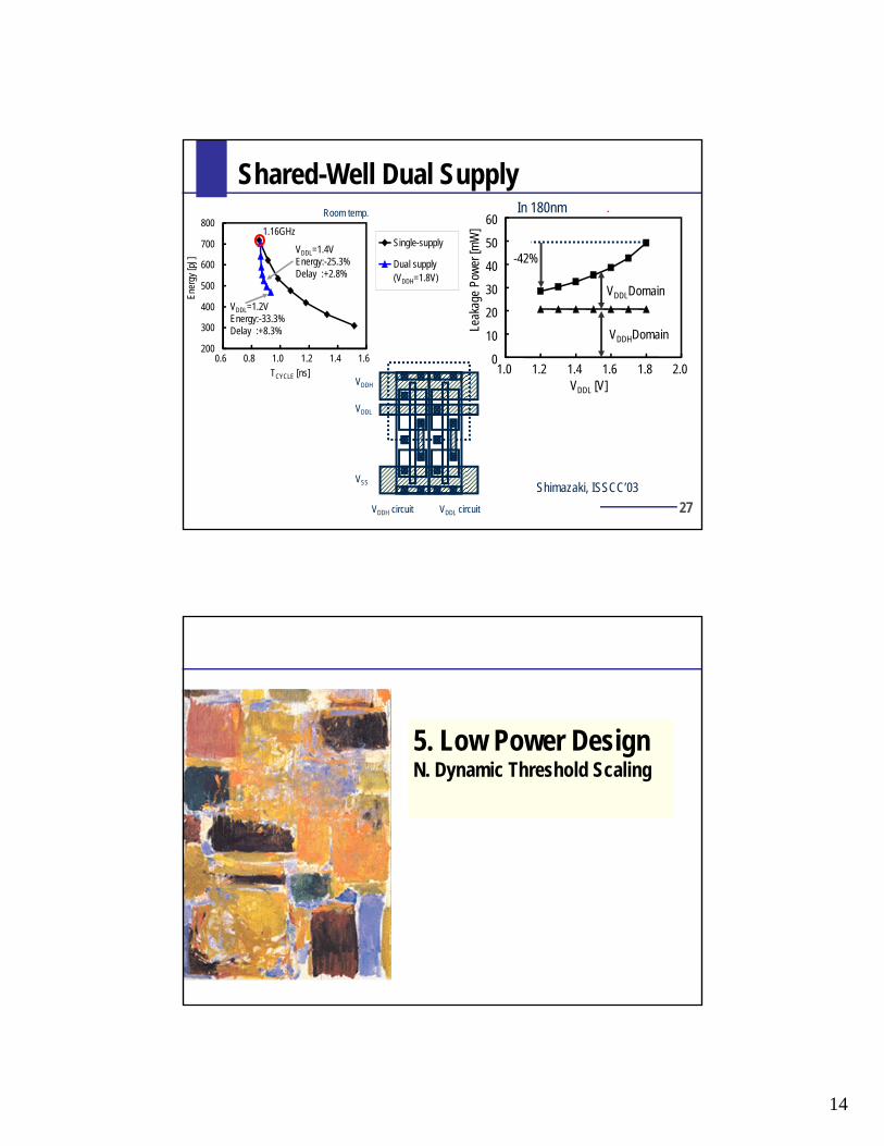
Shared-Well Dual Supply
VDDL [V]
Leak
age
Pow
er [m
W]
0
10
20
30
40
50
60
1.0 1.2 1.4 1.6 1.8 2.0
VDDHDomain
VDDLDomain
-42%
VDDH circuit
VDDH
VDDL
VSS
VDDL circuit
Ener
gy [p
J]
TCYCLE [ns]
Room temp.
200
300
400
500
600
700
800
0.6 0.8 1.0 1.2 1.4 1.6
Single-supply
Dual supply(VDDH=1.8V)
1.16GHz
VDDL=1.4VEnergy:-25.3% Delay :+2.8%
VDDL=1.2VEnergy:-33.3% Delay :+8.3%
Shimazaki, ISSCC’03
In 180nm
5. Low Power DesignN. Dynamic Threshold Scaling

15
29
Power /Energy Optimization SpaceConstant Throughput/Latency Variable Throughput/Latency
Energy Design Time Sleep Mode Run Time
Active
Logic design
Scaled VDD
Trans. sizing
Multi-VDD
Clock gatingDFS, DVS
Leakage
Stack effects
Trans sizing
Scaling VDD
+ Multi-VTh
Sleep T’s
Multi-VDD
Variable VTh
+ Input control
+ Variable VTh
30
Dynamic Body Bias
Similar concept to dynamic voltage scalingControl loop adjusts the substrate bias to meet the timing
Can be used just as runtime/sleep
Limited range of threshold adjustments (<100mV)Limited leakage reduction (<10x)No delay penalty
Can increase speed by forward bias
Energy cost of charging/discharging the substrate capacitance(but doesn’t need a regulator)

16
31
Dynamic Body Bias
32
Dynamic Body Bias
... ...
450mVFBB
450mVFBB
VCC
VSS
PMOSbody
NMOSbody
PMOSbias
NMOSbias
PMOSbias
... ...NMOS
bias
500mVRBB
500mVRBB
VCC
VSS
PMOSbody
NMOSbody
VHIGH
VLOW
Forward body bias (FBB)
Local VCC tracking
Active mode
Reverse body bias (RBB)
Triple well needed
Idle mode
Dual-VT
core
Tschanz, ISSCC’03
17
33
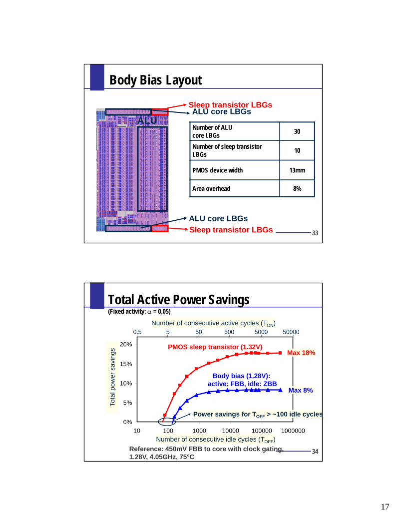
Body Bias Layout
Sleep transistor LBGs
Number of ALU core LBGs
30
Number of sleep transistor LBGs
10
PMOS device width 13mm
Area overhead 8%
ALU core LBGs
Sleep transistor LBGs
ALU core LBGs
ALU
34
0%
5%
10%
15%
20%
10 100 1000 10000 100000 1000000Number of idle cycles
To
tal p
ow
er
savi
ng
s
Total Active Power Savings(Fixed activity: = 0.05)
Body bias (1.28V): active: FBB, idle: ZBB
Reference: 450mV FBB to core with clock gating, 1.28V, 4.05GHz, 75°C
0.5 5 50 500 5000 50000
Number of consecutive idle cycles (TOFF)
Number of consecutive active cycles (TON)
Power savings for TOFF > ~100 idle cycles
PMOS sleep transistor (1.32V)
Tota
l pow
er s
avin
gs Max 18%
Max 8%

18
35
Body Biasing and Variations
Body biasing with a local control loop can be used to lower the impact of process variations
Used to limit die-to-die and within-die variations
36
Normalized Delay vs VDD & VTH
Sakurai, Kuroda
VTH (V)
0 0.2 0.4 0.7 1
1.5 V
3.0 V
5.0 V
0.6
1.0
1.4
1.8
No
rmal
ized
Del
ay ±0.15V
VDD =1.0 V
±0.05V
ΔVTH =
0.5
19
37
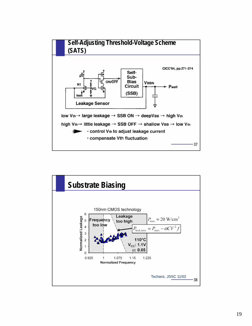
Self-Adjusting Threshold-Voltage Scheme (SATS)
38
Substrate Biasing
Tschanz, JSSC 11/02

20
39
Effectiveness of Substrate Bias
Die-to-die variations
40
Effectiveness of Substrate Bias
Within-die variations

21
41
Techniques Summary
0
20
40
60
80
100
0 0.2 0.4 0.6 0.8 1
Il ea
k(n
orm
aliz
ed
)
VDD [V]
Sleep transistor - up to~25x leakage reduction
Standby supply reduction~3-4x leakage reduction
Reverse bias~3x leakage
reduction
Standby supply + reverse bias~10x leakage reduction
Reduced VDD
Off-transistorload line
42
Next Lecture
Optimal supplies
Top Related