


Languages
Pages
Legal


ECE 442 – Jose Schutt‐Aine 1
ECE 442Solid‐State Devices & Circuits
16. Feedback
Jose E. Schutt-AineElectrical & Computer Engineering
University of [email protected]

ECE 442 – Jose Schutt‐Aine 2
• Why Use Feedback?
1. To desensitize the gain
2. To reduce nonlinear distortion
3. To reduce the effect of noise
4. To control terminal impedances
5. To increase the bandwidth
Feedback

ECE 442 – Jose Schutt‐Aine 3
Feedback – Basic Concepts

ECE 442 – Jose Schutt‐Aine 4
out
ia
vAv
=
out
in
vGv
=
out out
in ia
v vG Av v
= = =
0ia in inv v v= − =
The ideal amplifier gain is defined by
The overall gain of the feedback circuit is defined by
If input 2 is grounded
We then get
This is the open-loop gain
Feedback – Analysis

ECE 442 – Jose Schutt‐Aine 5
( )out in out inv A v v Gvβ= − =
1 β= =
+out
in
v AGv A
ia in outv v vβ= −
When the switch is closed, then
Feedback – Analysis
so that
from which we get
The closed-loop gain is always less than the open-loop gain for negative feedback
which is the closed-loop gain

ECE 442 – Jose Schutt‐Aine 6
( )1 /ω
=+
M
H
AA ss
The high-frequency response of an amplifier (single-pole) is given by:
Feedback – Bandwidth Extension
AM is the midband gain and ωH is the upper 3-dB frequency. With negative feedback, we get
( )( )1 ( )β
=+fA sA s
A s
/(1 )( )1 / (1 )
βω β
+=
+ +M M
fH M
A AA ss A
After substitution,

ECE 442 – Jose Schutt‐Aine 7
The feedback amplifier will have a midband gain of
Feedback – Bandwidth Extension
and an upper 3-dB frequency of
(1 )β+M
M
AA
(1 )ω β+H MA
Bandwidth is increased by factor equal to amount of feedback. It can also be shown that the lower 3dB frequency is
(1 )ω
β+L
MAThe gain-bandwidth product is constant

ECE 442 – Jose Schutt‐Aine 8
Series-Shunt Feedback
Voltage mixing-voltage sampling feedback

ECE 442 – Jose Schutt‐Aine 9
Shunt- Series Feedback
Current mixing-current sampling feedback

ECE 442 – Jose Schutt‐Aine 10
Series-Series Feedback
Voltage mixing-current sampling feedback

ECE 442 – Jose Schutt‐Aine 11
Shunt-Shunt Feedback
Current mixing-voltage sampling feedback

ECE 442 – Jose Schutt‐Aine 12
Transfer Function Representation
Use a two-terminal representation of system for input and output

ECE 442 – Jose Schutt‐Aine 13
Y-parameter Representation
1 11 1 12 2
2 21 1 22 2
I y V y VI y V y V
= += +

ECE 442 – Jose Schutt‐Aine 14
Y Parameter Calculations
2 2
1 211 21
1 10 0V V
I Iy yV V
= =
= =
To make V2= 0, place a short at port 2

ECE 442 – Jose Schutt‐Aine 15
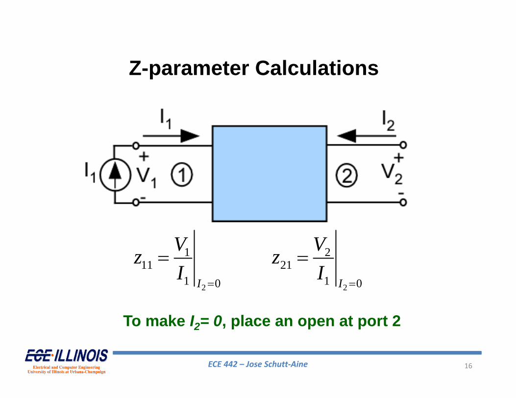
Z Parameters
1 11 1 12 2
2 21 1 22 2
V z I z IV z I z I
= += +
ECE 442 – Jose Schutt‐Aine 16
Z-parameter Calculations
2 2
1 211 21
1 10 0I I
V Vz zI I
= =
= =
To make I2= 0, place an open at port 2

ECE 442 – Jose Schutt‐Aine 17
H Parameters
1 11 1 12 2
2 21 1 22 2
V h I h VI h I h V
= += +

ECE 442 – Jose Schutt‐Aine 18
H Parameter Calculations
To make V2= 0, place a short at port 2
2 2
1 211 21
1 10 0V V
V Ih hI I
= =
= =

ECE 442 – Jose Schutt‐Aine 19
G Parameters
1 11 1 12 2
2 21 1 22 2
I g V g IV g V g I
= += +

ECE 442 – Jose Schutt‐Aine 20
G-Parameter Calculations
2 2
1 211 21
1 10 0I I
I Vg gV V
= =
= =
To make I2= 0, place an open at port 2

ECE 442 – Jose Schutt‐Aine 21
Series-Shunt Feedback - Ideal
1o
fs
V AAV Aβ
≡ =+
Negative feedback decreases the gain
o
i
VAV
≡

ECE 442 – Jose Schutt‐Aine 22
Series-Shunt Feedback – Equivalent Circuit
( )1if iR R Aβ= +
Negative feedback increases the input resistance and decreases the output resistance by a factor equal to the feedback
( )/ 1of oR R Aβ= +

ECE 442 – Jose Schutt‐Aine 23
Series-Shunt Feedback - Actual

ECE 442 – Jose Schutt‐Aine 24
Series-Shunt Feedback : h-Parameters
Account for all 4 h parameters

ECE 442 – Jose Schutt‐Aine 25
Series-Shunt Feedback : h-Parameters
12 12basic feedbackamplifier network
h h 21 21feedback basicnetwork amplifier
h h

ECE 442 – Jose Schutt‐Aine 26
Series-Series Feedback - Ideal
1o
fs
I AAV Aβ
≡ =+
Negative feedback decreases the gain
o
i
IAV
≡

ECE 442 – Jose Schutt‐Aine 27
Series-Series Feedback – Equivalent Circuit
( )1if iR R Aβ= + ( )1of oR R Aβ= +
Negative feedback increases the input resistance and increases the output resistance by a factor equal to the feedback

ECE 442 – Jose Schutt‐Aine 28
Series-Series Feedback - Actual

ECE 442 – Jose Schutt‐Aine 29
Series-Series Feedback: Z Parameters
Account for all 4 z parameters

ECE 442 – Jose Schutt‐Aine 30
12 12basic feedbackamplifier network
z z21 21feedback basic
network amplifierz z
Series-Series Feedback: Z Parameters

ECE 442 – Jose Schutt‐Aine 31
Shunt-Shunt Feedback - Ideal
o
i
VAI
≡

ECE 442 – Jose Schutt‐Aine 32
Shunt-Shunt Feedback
( )/ 1if iR R Aβ= + ( )/ 1of oR R Aβ= +
Negative feedback decreases the input resistance and decreases the output resistance by a factor equal to the feedback
12 12basic feedbackamplifier network
y y 21 21feedback basicnetwork amplifier
y y
1o
fs
V AAI Aβ
≡ =+
Negative feedback decreases the gain

ECE 442 – Jose Schutt‐Aine 33
Shunt-Series Feedback - Ideal
o
i
IAI
≡

ECE 442 – Jose Schutt‐Aine 34
Shunt-Series Feedback
( )/ 1if iR R Aβ= + ( )1of oR R Aβ= +
Negative feedback decreases the input resistance and increases the output resistance by a factor equal to the feedback
1o
fs
I AAI Aβ
≡ =+
Negative feedback decreases the gain
12 12basic feedbackamplifier network
g g 21 21feedback basicnetwork amplifier
g g

ECE 442 – Jose Schutt‐Aine 35
Rules for Series-Shunt Feedback
1 11 1 12 2
2 21 1 22 2
V h I h VI h I h V
= += +
2 2
1 211 21
1 10 0V V
V Ih hI I
= =
= =
1 1
1 212 22
2 20 0= =
= =I I
V Ih hV V

ECE 442 – Jose Schutt‐Aine 36
Rules for Series-Series Feedback
1 11 1 12 2
2 21 1 22 2
V z I z IV z I z I
= += +
2 2
1 211 21
1 10 0I I
V Vz zI I
= =
= =
1 1
1 212 22
2 20 0= =
= =I I
V Vz zI I

ECE 442 – Jose Schutt‐Aine 37
Rules for Shunt-Shunt Feedback
2 2
1 211 21
1 10 0V V
I Iy yV V
= =
= =
1 11 1 12 2
2 21 1 22 2
I y V y VI y V y V
= += +
1 1
1 212 22
2 20 0= =
= =V V
I Iy yV V

ECE 442 – Jose Schutt‐Aine 38
Rules for Shunt-Series Feedback
1 11 1 12 2
2 21 1 22 2
I g V g IV g V g I
= += +
2 2
1 211 21
1 10 0I I
I Vg gV V
= =
= =
1 1
1 212 22
2 20 0= =
= =V V
I Vg gI I

ECE 442 – Jose Schutt‐Aine 39
Example - Feedback
Differential stage followed by an emitter follower, with series-shunt feedback supplied by the resistors R1 and R2. Perform DC analysis and find A, β, Af, Rinand Rout

ECE 442 – Jose Schutt‐Aine 40
1 2 0.5= =E EI I mA
2 10.7 0.5 20 0.7= − × = +cV V
30.7 0= − =o BEV V
3 5=EI mA
1 2 50= = = ΩTe e
C
Vr rI
3 5= Ωer
Example - FeedbackModel asseries-shunt

ECE 442 – Jose Schutt‐Aine 41
( )( )2 3
31 1
1 2
20 || 1 (2 ||10) (2 ||10) 85.7 /10 (1|| 9) (2 ||10)1 1
β
β β
⎡ ⎤+ +⎣ ⎦= = × =++ + +
+ +
eo
s ee e
rVA V VV rr r
A - Circuit

ECE 442 – Jose Schutt‐Aine 42
1 2 4( 1)( ) ||β= + + + +i s e e ER R r r R R
( )10 101(50 50) 1|| 9 21= + + + = ΩiR k
32
202 ||10 || 1811β
⎡ ⎤= + = Ω⎢ ⎥+⎣ ⎦
o eR r
A - Circuit – cont’

ECE 442 – Jose Schutt‐Aine 43
' ' 1/ 0.19 1
β = = =+f oV V V
85.7 8.96 /1 1 85.7 0.1
of
s
V AA V VV Aβ
= = = =+ + ×
( )1 1 21 9.37 201ifR R A kβ= + = × = Ω
201 10 191IN if sR R R k= − = − = Ω
( ) 181|| 18.81 9.57
oof out L
RR R RAβ
= = = = Ω+
19.1outR = Ω
β - Circuit

ECE 442 – Jose Schutt‐Aine 44
3-Stage Amplifier with Feedback

ECE 442 – Jose Schutt‐Aine 45
3-Stage Amplifier with Feedback Model asseries-series

ECE 442 – Jose Schutt‐Aine 46
( )( )
1 1 21
1 1 2
Cc
i e E F E
R rVV r R R R
πα−=
⎡ ⎤+ +⎣ ⎦
Gain in first stage is:
First stage parameters are: IC1 = 0.6 mA, re1=41.7 Ω, Ic2=1 mA rπ2= hfe/gm2=100/40 = 2.5 kΩ
Use α1=0.99, Rc1=9 kΩ, RE1=100 Ω, RF=640 Ω, and RE2=100 Ω
1 14.92 /c
i
V V VV
= −
3-Stage Amplifier with Feedback

ECE 442 – Jose Schutt‐Aine 47
( ) ( )( ){ }22 2 3 2
1
1cm C fe e E F E
c
V g R h r R R RV
⎡ ⎤= − + + +⎣ ⎦
Gain in second stage is:
Use gm2=40 mA/V, RC2= 5 kΩ, hfe=100, re3=25/4,= 6.25 Ω, RE2=100 Ω, RF = 640 Ω, and RE1 = 100 Ω, which gives
2
1
131.2 /= −c
c
V V VV
3-Stage Amplifier with Feedback

ECE 442 – Jose Schutt‐Aine 48
( )( )3
2 3 3 2 1
1o e
c b e E F E
I IV V r R R R
= =+ +
Gain in third stage is:
Combining the 3 stages
314.92 131.2 10.6 10 20.7 /o
i
IA A VV
−= = − × − × × =
( )2
1 10.6 /6.25 100 740
o
c
I mA VV
= =+
3-Stage Amplifier with Feedback

ECE 442 – Jose Schutt‐Aine 49
21
2 1
f EE
o E F E
V R RI R R R
β = = ×+ +
determining feedback
100 100 11.9100 640 100
β = × = Ω+ +
3-Stage Amplifier with Feedback

ECE 442 – Jose Schutt‐Aine 50
20.7 83.7 /1 1 20.7 11.9
of
s
I AA mA VV Aβ
≡ = = =+ + ×
Closed-loop gain:
3 33
o C C o Cf C
s s s
V I R I R A RV V V
− −= = = −
383.7 10 600 50.2 /o
s
V V VV
−= − × × = −
3-Stage Amplifier with Feedback

ECE 442 – Jose Schutt‐Aine 51
( )1if iR R Aβ= +
Input resistance
( ) ( )1 1 21 13.65i fe e E F ER h r R R R k⎡ ⎤= + + + = Ω⎣ ⎦
( )13.65 1 20.5 11.9 3.34ifR M= + × = Ω
Output resistance
( ) 22 1 3 1
Co E F E e
fe
RR R R R rh
⎡ ⎤= + + +⎣ ⎦ +Ro=143.9 Ω
3-Stage Amplifier with Feedback

ECE 442 – Jose Schutt‐Aine 52
( )1 143.9(1 20.7 11.9) 35.6of oR R A kβ= + = + + = Ω
output resistance
( )( )3 31out o m o ofR r g r R rπ= + +
( )( )25 1 160 25 35.6 0.625 2.5outR M= + + × = Ω
3-Stage Amplifier with Feedback

ECE 442 – Jose Schutt‐Aine 53
Single-Stage Amplifier with Feedback We want to determine the small-signal voltage gain Vo/Vs, the input resistance and the output resistance Rout=Rof. The transistor has β = 100
Rin
Rof-
Vo
+
Rs = 10 kΩ
RF = 47 kΩRC = 4.7 kΩ
Vs
+12 V
Model asshunt-shunt

ECE 442 – Jose Schutt‐Aine 54
Single-Stage – DC AnalysisFirst determine dc operating point
0.7 ( 0.07)47= + +C BV I
3.99 47C BV I= +
( )12 1 0.074.7
CB
V Iβ−= + +
Solve for IB using the following 2 equations

ECE 442 – Jose Schutt‐Aine 55
Single-Stage – DC AnalysisWe get
0.015BI mA 1.5CI mA 4.7CV V
1.5 60 /25
Cm
T
Ig mA VV
= = =
/ 100 / 60 1.666mr g kπ β= = = Ω
10(1.66) 1.42911.6SR r kπ = = Ω
47(1.66) 1.648.66fR r kπ = = Ω

ECE 442 – Jose Schutt‐Aine 56
Calculating y11 for Amplifier
111 1 0.086 /
10 1.6S f
y mA VR R rπ
= = =+ +

ECE 442 – Jose Schutt‐Aine 57
221
1
IyV
=
( ) ( ) ( )1 11/f fm f
S f S f
V R r V R rv g R
R R r R R rπ π
ππ π
= = −+ +
Calculating y21 for Amplifier
( ) ( )21 1/ f
m fS f
R ry g R
R R rπ
π
= −+
( ) ( )12 1/ f
m fS f
V R rI g R
R R rπ
π
= −+

ECE 442 – Jose Schutt‐Aine 58
( )211.660 0.021 8.27 /
10 1.6y mA V= − =
+
Calculating y21 for Amplifier

ECE 442 – Jose Schutt‐Aine 59
Calculating y12 for Amplifier
( )( )
2112
2 2 2
1 1S
S f S S
V R rvIyV R V R R r R V
ππ
π
−−= = =
+
( )( )12
1 S
S f S
R ry
R R R rπ
π
= −+

ECE 442 – Jose Schutt‐Aine 60
( )121.429 0.00295 /
10 47 1.429y mA V= − = −
+
Calculating y12 for Amplifier

ECE 442 – Jose Schutt‐Aine 61
Calculating y22 for Amplifier
( )( ) ( )
22 22
m
m S
C S f S f
g v
g V R rV VIR R r R R r R
π
π
π π
= + ++ +
( )( ) ( )
222
2
1 1m S
C S f S f
g R rIyV R R r R R r R
π
π π
= = + ++ +
( )222
2
60 1.4291 1 2.01 /4.7 1.429 47 1.429 47
Iy mA VV
= = + + =+ +

ECE 442 – Jose Schutt‐Aine 62
111 0.021 /
f
y mA VR
= =
211 0.021 /
f
y mA VR
= − = −
22 11y y by symmetry=
12 21y y by reciprocity=
y-parameters for Feedback Network
From Feedback Network, we get β = y12 = -0.021

ECE 442 – Jose Schutt‐Aine 63
0.086 0.0038.27 2.01AY
−⎡ ⎤= ⎢ ⎥
⎣ ⎦
0.021 0.0210.021 0.021FY
−⎡ ⎤= ⎢ ⎥−⎣ ⎦
12 12basic feedbackamplifier network
y y
21 21feedback basicnetwork amplifier
y y
Feedback NetworkBasic Amplifier
Basic Amplifier vs Feedback Network
ECE 442 – Jose Schutt‐Aine 64
Single-Stage – Small-Signal Analysis

ECE 442 – Jose Schutt‐Aine 65
Single-Stage – Small-Signal AnalysisThe feedback is provided by Rf which samples the output voltage and feeds back a current to be mixed at input
( )i s fV I R R rπ π=
( )o m f CV g V R Rπ= −
( )( ) 358.7om f C s f
i
VA g R R R R r kI π= = − = − Ω
Transimpedance gain is –358.7 kΩ

ECE 442 – Jose Schutt‐Aine 66
Input and Output Resistances
1.4i s fR R R r kπ= = Ω
4.27o C fR R R k= = Ω

ECE 442 – Jose Schutt‐Aine 67
Determining β and Af
1 147
f
o f
IV R k
β = = − = −Ω
1o
fs
V AAI Aβ
≡ =+
358.7 358.7 41.61 358.7 / 47 8.63
o
s
V kI
− −= = = − Ω
+

ECE 442 – Jose Schutt‐Aine 68
Voltage gain is:
Single-Stage Feedback Amp
41.6 4.16 /10
o o
s s s
V V V VV I R
−= = −
The input resistance with feedback is:
1.4 162.21 8.63
iif
RRAβ
= = = Ω+
The output resistance with feedback is:4.27 495
1 8.63o
ofRRAβ
= = = Ω+

ECE 442 – Jose Schutt‐Aine 69
1. Most of the forward transmission occurs in the basic amplifier
2. Most of the feedback -or reverse transmission - occurs in the feedback network
3. Care should be taken in the design that these assumptions are valid
Important Remarks

ECE 442 – Jose Schutt‐Aine 70
1. The closed-loop transfer function is a function of frequency
2. The manner in which the loop gain varies with frequency determines the stability or instability of the feedback amplifier
3. The frequency at which the phase of the transfer function is equal to 180o will be unstable if the magnitude is greater than unity
Feedback and Frequency Dependence

ECE 442 – Jose Schutt‐Aine 71
1. An amplifier with a single pole response is unconditionally stable
2. An amplifier with a two-pole response is unconditionally stable
3. An amplifier with a three-pole response (or higher) can be unstable need to provide compensation
Feedback and Frequency Dependence

ECE 442 – Jose Schutt‐Aine 72
1. In order to insure stability, we modify the open-loop transfer function A(s) of the amplifier
2. Introduce a new pole in the function A(s) at a frequency fD such that modified open-loop gain A’(s) intersects the 20 log |1/|β|) curve with a a slope difference of 20 dB/decade
3. The closed-loop amplifier with β value (or lower) will be stable.
Feedback and Frequency Compensation

ECE 442 – Jose Schutt‐Aine 73
Feedback and Frequency Compensation

ECE 442 – Jose Schutt‐Aine 74
Miller Compensation
Common emitter amplifier with Miller compensating capacitor Cf in feedback path

ECE 442 – Jose Schutt‐Aine 75
Miller Compensation and Pole Splitting
R1 and C1 make up the total input impedance; R2and C2 make up the total output impedance
In the absence of the compensating capacitor, Cf, there are two poles associated with C1 and C2 fp1and fp2

ECE 442 – Jose Schutt‐Aine 76
Miller Compensation and Pole Splitting
1 21 1 2 2
1 12 2P Pf f
R C R Cπ π= =
( ) 1 221
f mo
i
sC g R RVI sA s B
−=
+ +
When Cf is present, the transfer function becomes
( )1 1 2 2 1 2 1 2f mA C R C R C g R R R R= + + + +
( )1 2 1 2 1 2fB C C C C C R R⎡ ⎤= + +⎣ ⎦

ECE 442 – Jose Schutt‐Aine 77
Pole Splitting
( )' '1 2
2 1 1 2 1 2
1 m fP P
m f f
g Cand
g R C R C C C C Cω ω
+ +
The two poles can be approximated as:
When Cf is increased, ω’P1 is reduced while ω’P2 is increased this is referred to as pole splitting
Top Related