


Languages
Pages
Legal

DRV8302PWM
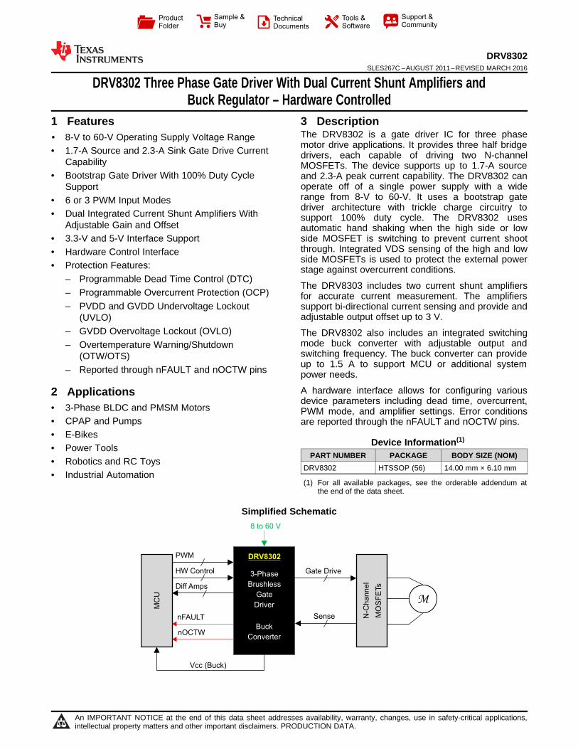
8 to 60 V
MC
U
N-C
ha
nn
el
MO
SF
ETs
Gate Drive
Sense
3-Phase
Brushless
Gate
Driver
Buck
Converter
HW Control
nFAULT
nOCTW
Vcc (Buck)
Diff Amps
M
Product
Folder
Sample &Buy
Technical
Documents
Tools &
Software
Support &Community
An IMPORTANT NOTICE at the end of this data sheet addresses availability, warranty, changes, use in safety-critical applications,intellectual property matters and other important disclaimers. PRODUCTION DATA.
DRV8302SLES267C –AUGUST 2011–REVISED MARCH 2016
DRV8302 Three Phase Gate Driver With Dual Current Shunt Amplifiers andBuck Regulator – Hardware Controlled
1
1 Features1• 8-V to 60-V Operating Supply Voltage Range• 1.7-A Source and 2.3-A Sink Gate Drive Current
Capability• Bootstrap Gate Driver With 100% Duty Cycle
Support• 6 or 3 PWM Input Modes• Dual Integrated Current Shunt Amplifiers With
Adjustable Gain and Offset• 3.3-V and 5-V Interface Support• Hardware Control Interface• Protection Features:
– Programmable Dead Time Control (DTC)– Programmable Overcurrent Protection (OCP)– PVDD and GVDD Undervoltage Lockout
(UVLO)– GVDD Overvoltage Lockout (OVLO)– Overtemperature Warning/Shutdown
(OTW/OTS)– Reported through nFAULT and nOCTW pins
2 Applications• 3-Phase BLDC and PMSM Motors• CPAP and Pumps• E-Bikes• Power Tools• Robotics and RC Toys• Industrial Automation
3 DescriptionThe DRV8302 is a gate driver IC for three phasemotor drive applications. It provides three half bridgedrivers, each capable of driving two N-channelMOSFETs. The device supports up to 1.7-A sourceand 2.3-A peak current capability. The DRV8302 canoperate off of a single power supply with a widerange from 8-V to 60-V. It uses a bootstrap gatedriver architecture with trickle charge circuitry tosupport 100% duty cycle. The DRV8302 usesautomatic hand shaking when the high side or lowside MOSFET is switching to prevent current shootthrough. Integrated VDS sensing of the high and lowside MOSFETs is used to protect the external powerstage against overcurrent conditions.
The DRV8303 includes two current shunt amplifiersfor accurate current measurement. The amplifierssupport bi-directional current sensing and provide andadjustable output offset up to 3 V.
The DRV8302 also includes an integrated switchingmode buck converter with adjustable output andswitching frequency. The buck converter can provideup to 1.5 A to support MCU or additional systempower needs.
A hardware interface allows for configuring variousdevice parameters including dead time, overcurrent,PWM mode, and amplifier settings. Error conditionsare reported through the nFAULT and nOCTW pins.
Device Information(1)
PART NUMBER PACKAGE BODY SIZE (NOM)DRV8302 HTSSOP (56) 14.00 mm × 6.10 mm
(1) For all available packages, see the orderable addendum atthe end of the data sheet.
Simplified Schematic
2
DRV8302SLES267C –AUGUST 2011–REVISED MARCH 2016 www.ti.com
Product Folder Links: DRV8302
Submit Documentation Feedback Copyright © 2011–2016, Texas Instruments Incorporated
Table of Contents1 Features .................................................................. 12 Applications ........................................................... 13 Description ............................................................. 14 Revision History..................................................... 25 Pin Configuration and Functions ......................... 36 Specifications......................................................... 5
6.1 Absolute Maximum Ratings ...................................... 56.2 ESD Ratings.............................................................. 56.3 Recommended Operating Conditions....................... 66.4 Thermal Information .................................................. 66.5 Electrical Characteristics........................................... 76.6 Gate Timing and Protection Characteristics ............. 86.7 Current Shunt Amplifier Characteristics.................... 86.8 Buck Converter Characteristics ................................ 96.9 Typical Characteristics ............................................ 10
7 Detailed Description ............................................ 117.1 Overview ................................................................. 117.2 Function Block Diagram.......................................... 12
7.3 Feature Description................................................. 137.4 Device Functional Modes........................................ 19
8 Application and Implementation ........................ 208.1 Application Information............................................ 208.2 Typical Application ................................................. 21
9 Power Supply Recommendations ...................... 249.1 Bulk Capacitance .................................................... 24
10 Layout................................................................... 2510.1 Layout Guidelines ................................................. 2510.2 Layout Example .................................................... 25
11 Device and Documentation Support ................. 2611.1 Documentation Support ........................................ 2611.2 Community Resources.......................................... 2611.3 Trademarks ........................................................... 2611.4 Electrostatic Discharge Caution............................ 2611.5 Glossary ................................................................ 26
12 Mechanical, Packaging, and OrderableInformation ........................................................... 26
4 Revision HistoryNOTE: Page numbers for previous revisions may differ from page numbers in the current version.
Changes from Revision B (February 2016) to Revision C Page
• Deleted REG 0x02 from the test conditions of the Ioso1 and Iosi1 parameters in the Electrical Characteristics table ............ 7• Changed the value of R1 + R2 ≥ 100 KΩ to R1 + R2 ≥ 1 KΩ in the OC_ADJ section. ....................................................... 17
Changes from Revision A (December 2015) to Revision B Page
• Changed VEN_BUCK in Buck Converter Characteristics From: MIN = 0.9 V and MAX = 1.55 V To: MIN = 1.11 Vand MAX = 1.36 V. ................................................................................................................................................................ 9
Changes from Original (August 2011) to Revision A Page
• Added Pin Configuration and Functions section, ESD Rating table, Feature Description section, Device FunctionalModes, Application and Implementation section, Power Supply Recommendations section, Layout section, Deviceand Documentation Support section, and Mechanical, Packaging, and Orderable Information section .............................. 1
• VPVDD absolute max voltage rating reduced from 70 V to 65 V ............................................................................................. 5• Clarification made on how the OCP status bits report in Overcurrent Protection (OCP) and Reporting ............................ 16• Update to PVDD1 undervoltage protection in Undervoltage Protection (UVLO) describing specific transient brownout
issue. ................................................................................................................................................................................... 17• Update to EN_GATE pin functional description in EN_GATE clarifying proper EN_GATE reset pulse lengths. ................ 19• Added gate driver power-up sequencing errata Gate Driver Power Up Sequencing Errdata.............................................. 20• Added Community Resources ............................................................................................................................................. 24
1RT_CLK2
3
4
12
5
6
7
8
9
10
11
13
14
15
16
17
18
26
19
20
21
22
23
24
25
27
28
56
55
54
53
45
52
51
50
49
48
47
46
44
43
42
41
40
39
31
38
37
36
35
34
33
32
30
29
COMPVSENSEPWRGDnOCTWnFAULT
DTCM_PWM
M_OC
DC_CAL
GAINOC_ADJ
GVDDCP1CP2
EN_GATEINH_AINL_AINH_BINL_BINH_CINL_CDVDD
REFSO1SO2
AVDDAGND
SS_TREN_BUCKPVDD2PVDD2BST_BKPHPHBIASBST_A
GL_A
GH_ASH_A
SL_ABST_BGH_BSH_BGL_BSL_BBST_CGH_CSH_CGL_CSL_CSN1SP1SN2SP2PVDD1
GN
D (
57)
- P
ow
erP
AD
3
DRV8302www.ti.com SLES267C –AUGUST 2011–REVISED MARCH 2016
Product Folder Links: DRV8302
Submit Documentation FeedbackCopyright © 2011–2016, Texas Instruments Incorporated
(1) KEY: I =Input, O = Output, P = Power
5 Pin Configuration and Functions
DCA Package56-Pin HTSSOP With PowerPAD™
Top View
Pin FunctionsPIN
I/O (1) DESCRIPTIONNO. NAME
1 RT_CLK I Resistor timing and external clock for buck regulator. Resistor should connect to GND (PowerPAD™)with very short trace to reduce the potential clock jitter due to noise.
2 COMP O Buck error amplifier output and input to the output switch current comparator.3 VSENSE I Buck output voltage sense pin. Inverting node of error amplifier.
4 PWRGD I An open drain output with external pullup resistor required. Asserts low if buck output voltage is lowdue to thermal shutdown, dropout, overvoltage, or EN_BUCK shut down
5 nOCTW O Overcurrent and overtemperature warning indicator. This output is open drain with external pullupresistor required.
6 nFAULT O Fault report indicator. This output is open drain with external pullup resistor required.7 DTC I Dead-time adjustment with external resistor to GND
8 M_PWM I
Mode selection pin for PWM input configuration. If M_PWM = LOW, the device supports 6 independentPWM inputs. When M_PWM = HIGH, the device must be connected to ONLY 3 PWM input signals onINH_x. The complementary PWM signals for low side signaling will be internally generated from thehigh side inputs.
9 M_OC IMode selection pin for over-current protection options. If M_OC = LOW, the gate driver will operate in acycle-by-cycle current limiting mode. If M_OC = HIGH, the gate driver will shutdown the channel whichdetected an over-current event.
10 GAIN O Gain selection for integrated current shunt amplifiers. If GAIN = LOW, the internal current shuntamplifiers have a gain of 10V/V. If GAIN = HIGH, the current shunt amplifiers have a gain of 40V/V.
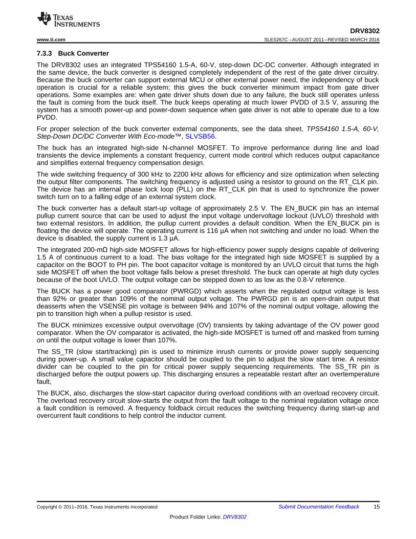
11 OC_ADJ I Overcurrent trip set pin. Apply a voltage on this pin to set the trip point for the internal overcurrentprotection circuitry. A voltage divider from DVDD is recommended.
12 DC_CAL I When DC_CAL is high, device shorts inputs of shunt amplifiers and disconnects loads. DC offsetcalibration can be done through external microcontroller.
4
DRV8302SLES267C –AUGUST 2011–REVISED MARCH 2016 www.ti.com
Product Folder Links: DRV8302
Submit Documentation Feedback Copyright © 2011–2016, Texas Instruments Incorporated
Pin Functions (continued)PIN
I/O (1) DESCRIPTIONNO. NAME13 GVDD P Internal gate driver voltage regulator. GVDD cap should connect to GND14 CP1 P Charge pump pin 1, ceramic cap should be used between CP1 and CP215 CP2 P Charge pump pin 2, ceramic cap should be used between CP1 and CP216 EN_GATE I Enable gate driver and current shunt amplifiers. Control buck via EN_BUCK pin.17 INH_A I PWM Input signal (high side), half-bridge A18 INL_A I PWM Input signal (low side), half-bridge A19 INH_B I PWM Input signal (high side), half-bridge B20 INL_B I PWM Input signal (low side), half-bridge B21 INH_C I PWM Input signal (high side), half-bridge C22 INL_C I PWM Input signal (low side), half-bridge C
23 DVDD P Internal 3.3-V supply voltage. DVDD cap should connect to AGND. This is an output, but not specifiedto drive external circuitry.
24 REF I Reference voltage to set output of shunt amplfiiers with a bias voltage which equals to half of thevoltage set on this pin. Connect to ADC reference in microcontroller.
25 SO1 O Output of current amplifier 126 SO2 O Output of current amplifier 2
27 AVDD P Internal 6-V supply voltage, AVDD cap should connect to AGND. This is an output, but not specified todrive external circuitry.
28 AGND P Analog ground pin
29 PVDD1 P Power supply pin for gate driver and current shunt amplifier. PVDD1 is independent of buck powersupply, PVDD2. PVDD1 cap should connect to GND
30 SP2 I Input of current amplifier 2 (connecting to positive input of amplifier). Recommend to connect to groundside of the sense resistor for the best commom mode rejection.
31 SN2 I Input of current amplifier 2 (connecting to negative input of amplifier).
32 SP1 I Input of current amplifier 1 (connecting to positive input of amplifier). Recommend to connect to groundside of the sense resistor for the best commom mode rejection.
33 SN1 I Input of current amplifier 1 (connecting to negative input of amplifier).
34 SL_C I Low-Side MOSFET source connection, half-bridge C. Low-side VDS measured between this pin andSH_C.
35 GL_C O Gate drive output for Low-Side MOSFET, half-bridge C
36 SH_C I High-Side MOSFET source connection, half-bridge C. High-side VDS measured between this pin andPVDD1.
37 GH_C O Gate drive output for High-Side MOSFET, half-bridge C38 BST_C P Bootstrap cap pin for half-bridge C
39 SL_B I Low-Side MOSFET source connection, half-bridge B. Low-side VDS measured between this pin andSH_B.
40 GL_B O Gate drive output for Low-Side MOSFET, half-bridge B
41 SH_B I High-Side MOSFET source connection, half-bridge B. High-side VDS measured between this pin andPVDD1.
42 GH_B O Gate drive output for High-Side MOSFET, half-bridge B43 BST_B P Bootstrap cap pin for half-bridge B
44 SL_A I Low-Side MOSFET source connection, half-bridge A. Low-side VDS measured between this pin andSH_A.
45 GL_A O Gate drive output for Low-Side MOSFET, half-bridge A
46 SH_A I High-Side MOSFET source connection, half-bridge A. High-side VDS measured between this pin andPVDD1.
47 GH_A O Gate drive output for High-Side MOSFET, half-bridge A48 BST_A P Bootstrap cap pin for half-bridge A49 BIAS I Bias pin. Connect 1M-Ω resistor to GND, or 0.1 µF capacitor to GND.50, 51 PH O The source of the internal high side MOSFET of buck converter
5
DRV8302www.ti.com SLES267C –AUGUST 2011–REVISED MARCH 2016
Product Folder Links: DRV8302
Submit Documentation FeedbackCopyright © 2011–2016, Texas Instruments Incorporated
Pin Functions (continued)PIN
I/O (1) DESCRIPTIONNO. NAME52 BST_BK P Bootstrap cap pin for buck converter53, 54 PVDD2 P Power supply pin for buck converter, PVDD2 cap should connect to GND.
55 EN_BUCK I Enable buck converter. Internal pullup current source. Pull below 1.2 V to disable. Float to enable.Adjust the input undervoltage lockout with two resistors
56 SS_TR IBuck soft-start and tracking. An external capacitor connected to this pin sets the output rise time. Sincethe voltage on this pin overrides the internal reference, it can be used for tracking and sequencing. Capshould connect to GND
57 GND(PWR_PAD) P
GND pin. The exposed power pad must be electrically connected to ground plane through soldering toPCB for proper operation and connected to bottom side of PCB through vias for better thermalspreading.
(1) Stresses beyond those listed under Absolute Maximum Ratings may cause permanent damage to the device. These are stress ratingsonly, which do not imply functional operation of the device at these or any other conditions beyond those indicated under RecommendedOperating Conditions. Exposure to absolute-maximum-rated conditions for extended periods may affect device reliability.
6 Specifications
6.1 Absolute Maximum Ratingsover operating free-air temperature range (unless otherwise noted) (1)
MIN MAX UNITVPVDD Supply voltage Relative to PGND –0.3 65 VPVDDRAMP Maximum supply voltage ramp rate Voltage rising up to PVDDMAX 1 V/µsVPGND Maximum voltage between PGND and GND –0.3 0.3 VIIN_MAX Maximum current, all digital and analog input pins except nFAULT and nOCTW pins –1 1 mAIIN_OD_MAX Maximum sinking current for open-drain pins (nFAULT and nOCTW Pins) 7 mAVOPA_IN Voltage range for SPx and SNx pins –0.6 0.6 V
VLOGICInput voltage range for logic/digital pins (INH_A, INL_A, INH_B, INL_B, INH_C, INL_C,EN_GATE, M_PWM, M_OC, OC_ADJ, GAIN, DC_CAL) –0.3 7 V
VGVDD Maximum voltage for GVDD pin 13.2 VVAVDD Maximum voltage for AVDD pin 8 VVDVDD Maximum voltage for DVDD pin 3.6 VVREF Maximum reference voltage for current amplifier 7 VIREF Maximum current for REF Pin 100 µATJ Maximum operating junction temperature –40 150 °CTstg Storage temperature –55 150 °C
(1) JEDEC document JEP155 states that 500-V HBM allows safe manufacturing with a standard ESD control process.(2) JEDEC document JEP157 states that 250-V CDM allows safe manufacturing with a standard ESD control process.
6.2 ESD RatingsVALUE UNIT
V(ESD)Electrostaticdischarge
Human-body model (HBM), per ANSI/ESDA/JEDEC JS-001 (1) ±2000V
Charged-device model (CDM), per JEDEC specification JESD22-C101 (2) ±500
6
DRV8302SLES267C –AUGUST 2011–REVISED MARCH 2016 www.ti.com
Product Folder Links: DRV8302
Submit Documentation Feedback Copyright © 2011–2016, Texas Instruments Incorporated
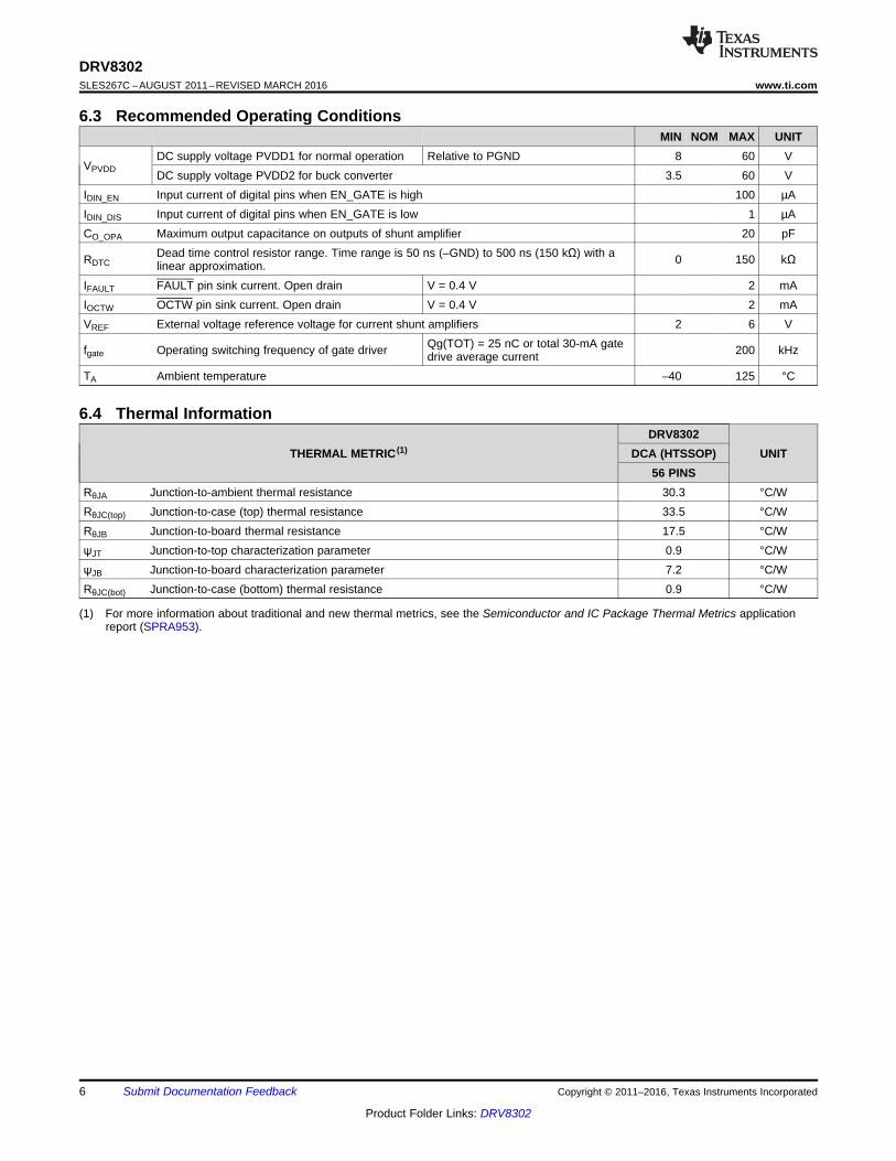
6.3 Recommended Operating ConditionsMIN NOM MAX UNIT
VPVDDDC supply voltage PVDD1 for normal operation Relative to PGND 8 60 VDC supply voltage PVDD2 for buck converter 3.5 60 V
IDIN_EN Input current of digital pins when EN_GATE is high 100 µAIDIN_DIS Input current of digital pins when EN_GATE is low 1 µACO_OPA Maximum output capacitance on outputs of shunt amplifier 20 pF
RDTCDead time control resistor range. Time range is 50 ns (–GND) to 500 ns (150 kΩ) with alinear approximation. 0 150 kΩ
IFAULT FAULT pin sink current. Open drain V = 0.4 V 2 mAIOCTW OCTW pin sink current. Open drain V = 0.4 V 2 mAVREF External voltage reference voltage for current shunt amplifiers 2 6 V
fgate Operating switching frequency of gate driver Qg(TOT) = 25 nC or total 30-mA gatedrive average current 200 kHz
TA Ambient temperature –40 125 °C
(1) For more information about traditional and new thermal metrics, see the Semiconductor and IC Package Thermal Metrics applicationreport (SPRA953).
6.4 Thermal Information
THERMAL METRIC (1)DRV8302
UNITDCA (HTSSOP)56 PINS
RθJA Junction-to-ambient thermal resistance 30.3 °C/WRθJC(top) Junction-to-case (top) thermal resistance 33.5 °C/WRθJB Junction-to-board thermal resistance 17.5 °C/WψJT Junction-to-top characterization parameter 0.9 °C/WψJB Junction-to-board characterization parameter 7.2 °C/WRθJC(bot) Junction-to-case (bottom) thermal resistance 0.9 °C/W
7
DRV8302www.ti.com SLES267C –AUGUST 2011–REVISED MARCH 2016
Product Folder Links: DRV8302
Submit Documentation FeedbackCopyright © 2011–2016, Texas Instruments Incorporated
6.5 Electrical CharacteristicsPVDD = 8 V to 60 V, TC = 25°C, unless specified under test condition
PARAMETER TEST CONDITIONS MIN TYP MAX UNITINPUT PINS: INH_X, INL_X, M_PWM, M_OC, GAIN, EN_GATE, DC_CALVIH High input threshold 2 VVIL Low input threshold 0.8 VREN_GATE Internal pulldown resistor for EN_GATE 100 kΩ
RINH_XInternal pulldown resistor for high side PWMs(INH_A, INH_B, and INH_C) EN_GATE high 100 kΩ
RINH_XInternal pulldown resistor for low side PWMs(INL_A, INL_B, and INL_C) EN_GATE high 100 kΩ
RM_PWM Internal pulldown resistor for M_PWM EN_GATE high 100 kΩRM_OC Internal pulldown resistor for M_OC EN_GATE high 100 kΩRDC_CAL Internal pulldown resistor for DC_CAL EN_GATE high 100 kΩOUTPUT PINS: nFAULT AND nOCTWVOL Low output threshold IO = 2 mA 0.4 V
VOH High output threshold External 47-kΩ pullup resistor connected to3-5.5 V 2.4 V
IOHLeakage current on open-drain pins When logichigh (nFAULT and nOCTW) 1 µA
GATE DRIVE OUTPUT: GH_A, GH_B, GH_C, GL_A, GL_B, GL_CVGX_NORM Gate driver Vgs voltage PVDD = 8 V to 60 V 9.5 11.5 VIoso1 Maximum source current setting 1, peak Vgs of FET equals to 2 V 1.7 AIosi1 Maximum sink current setting 1, peak Vgs of FET equals to 8 V 2.3 A
Rgate_offGate output impedance during standby modewhen EN_GATE low (pins GH_x, GL_x) 1.6 2.4 kΩ
SUPPLY CURRENTSIPVDD1_STB PVDD1 supply current, standby EN_GATE is low. PVDD1 = 8 V. 20 50 µA
IPVDD1_OP PVDD1 supply current, operatingEN_GATE is high, no load on gate driveoutput, switching at 10 kHz,100-nC gate charge
15 mA
IPVDD1_HIZ PVDD1 Supply current, HiZ EN_GATE is high, gate not switching 2 5 11 mAINTERNAL REGULATOR VOLTAGEAVDD AVDD voltage 6 6.5 7 VDVDD DVDD voltage 3 3.3 3.6 VVOLTAGE PROTECTIONVPVDD_UV Undervoltage protection limit, PVDD 6 VVGVDD_UV Undervoltage protection limit, GVDD 8 VVGVDD_OV Overvoltage protection limit, GVDD 16 VCURRENT PROTECTION, (VDS SENSING)VDS_OC Drain-source voltage protection limit 0.125 2.4 VToc OC sensing response time 1.5 µs
TOC_PULSEOCTW pin reporting pulse stretch length for OCevent 64 µs
8
DRV8302SLES267C –AUGUST 2011–REVISED MARCH 2016 www.ti.com
Product Folder Links: DRV8302
Submit Documentation Feedback Copyright © 2011–2016, Texas Instruments Incorporated
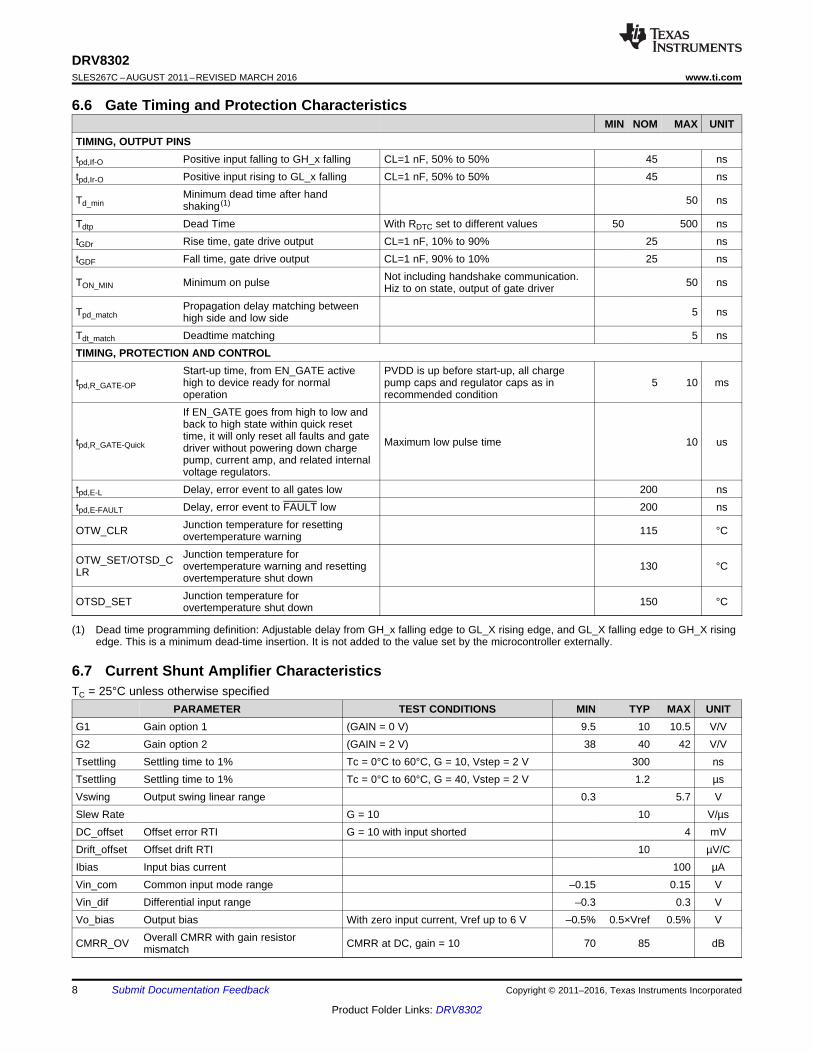
(1) Dead time programming definition: Adjustable delay from GH_x falling edge to GL_X rising edge, and GL_X falling edge to GH_X risingedge. This is a minimum dead-time insertion. It is not added to the value set by the microcontroller externally.
6.6 Gate Timing and Protection CharacteristicsMIN NOM MAX UNIT
TIMING, OUTPUT PINStpd,If-O Positive input falling to GH_x falling CL=1 nF, 50% to 50% 45 nstpd,Ir-O Positive input rising to GL_x falling CL=1 nF, 50% to 50% 45 ns
Td_minMinimum dead time after handshaking (1) 50 ns
Tdtp Dead Time With RDTC set to different values 50 500 nstGDr Rise time, gate drive output CL=1 nF, 10% to 90% 25 nstGDF Fall time, gate drive output CL=1 nF, 90% to 10% 25 ns
TON_MIN Minimum on pulse Not including handshake communication.Hiz to on state, output of gate driver 50 ns
Tpd_matchPropagation delay matching betweenhigh side and low side 5 ns
Tdt_match Deadtime matching 5 nsTIMING, PROTECTION AND CONTROL
tpd,R_GATE-OP
Start-up time, from EN_GATE activehigh to device ready for normaloperation
PVDD is up before start-up, all chargepump caps and regulator caps as inrecommended condition
5 10 ms
tpd,R_GATE-Quick
If EN_GATE goes from high to low andback to high state within quick resettime, it will only reset all faults and gatedriver without powering down chargepump, current amp, and related internalvoltage regulators.
Maximum low pulse time 10 us
tpd,E-L Delay, error event to all gates low 200 nstpd,E-FAULT Delay, error event to FAULT low 200 ns
OTW_CLR Junction temperature for resettingovertemperature warning 115 °C
OTW_SET/OTSD_CLR
Junction temperature forovertemperature warning and resettingovertemperature shut down
130 °C
OTSD_SET Junction temperature forovertemperature shut down 150 °C
6.7 Current Shunt Amplifier CharacteristicsTC = 25°C unless otherwise specified
PARAMETER TEST CONDITIONS MIN TYP MAX UNITG1 Gain option 1 (GAIN = 0 V) 9.5 10 10.5 V/VG2 Gain option 2 (GAIN = 2 V) 38 40 42 V/VTsettling Settling time to 1% Tc = 0°C to 60°C, G = 10, Vstep = 2 V 300 nsTsettling Settling time to 1% Tc = 0°C to 60°C, G = 40, Vstep = 2 V 1.2 µsVswing Output swing linear range 0.3 5.7 VSlew Rate G = 10 10 V/µsDC_offset Offset error RTI G = 10 with input shorted 4 mVDrift_offset Offset drift RTI 10 µV/CIbias Input bias current 100 µAVin_com Common input mode range –0.15 0.15 VVin_dif Differential input range –0.3 0.3 VVo_bias Output bias With zero input current, Vref up to 6 V –0.5% 0.5×Vref 0.5% V
CMRR_OV Overall CMRR with gain resistormismatch CMRR at DC, gain = 10 70 85 dB
9
DRV8302www.ti.com SLES267C –AUGUST 2011–REVISED MARCH 2016
Product Folder Links: DRV8302
Submit Documentation FeedbackCopyright © 2011–2016, Texas Instruments Incorporated
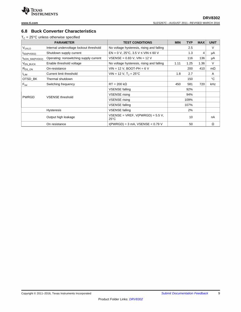
6.8 Buck Converter CharacteristicsTC = 25°C unless otherwise specified
PARAMETER TEST CONDITIONS MIN TYP MAX UNITVUVLO Internal undervoltage lockout threshold No voltage hysteresis, rising and falling 2.5 VISD(PVDD2) Shutdown supply current EN = 0 V, 25°C, 3.5 V ≤ VIN ≤ 60 V 1.3 4 µAINON_SW(PVDD2) Operating: nonswitching supply current VSENSE = 0.83 V, VIN = 12 V 116 136 µAVEN_BUCK Enable threshold voltage No voltage hysteresis, rising and falling 1.11 1.25 1.36 VRDS_ON On-resistance VIN = 12 V, BOOT-PH = 6 V 200 410 mΩILIM Current limit threshold VIN = 12 V, TJ = 25°C 1.8 2.7 AOTSD_BK Thermal shutdown 150 °CFsw Switching frequency RT = 200 kΩ 450 581 720 kHz
PWRGD VSENSE threshold
VSENSE falling 92%VSENSE rising 94%VSENSE rising 109%VSENSE falling 107%
Hysteresis VSENSE falling 2%
Output high leakage VSENSE = VREF, V(PWRGD) = 5.5 V,25°C 10 nA
On resistance I(PWRGD) = 3 mA, VSENSE < 0.79 V 50 Ω
10.0
10.2
10.4
10.6
10.8
11.0
11.2
11.4
11.6
11.8
12.0
-40 0 25 85 125
GV
DD
(V
)
Temperature (C) C001
8.0
8.2
8.4
8.6
8.8
9.0
9.2
9.4
9.6
9.8
10.0
-40 0 25 85 125
I PV
DD
1 (µ
A)
Temperature (C) C001
10.0
10.2
10.4
10.6
10.8
11.0
11.2
11.4
11.6
11.8
12.0
-40 0 25 85 125
GV
DD
(V
)
Temperature (C) C002
10
DRV8302SLES267C –AUGUST 2011–REVISED MARCH 2016 www.ti.com
Product Folder Links: DRV8302
Submit Documentation Feedback Copyright © 2011–2016, Texas Instruments Incorporated
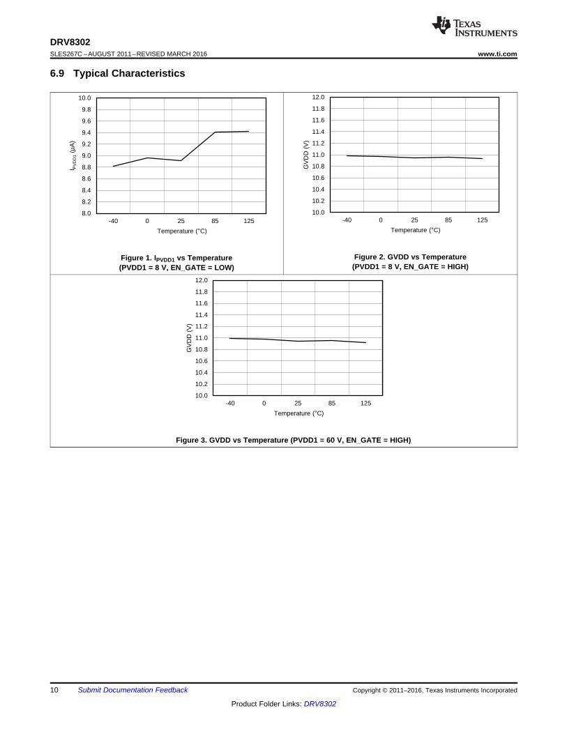
6.9 Typical Characteristics
Figure 1. IPVDD1 vs Temperature(PVDD1 = 8 V, EN_GATE = LOW)
Figure 2. GVDD vs Temperature(PVDD1 = 8 V, EN_GATE = HIGH)
Figure 3. GVDD vs Temperature (PVDD1 = 60 V, EN_GATE = HIGH)

11
DRV8302www.ti.com SLES267C –AUGUST 2011–REVISED MARCH 2016
Product Folder Links: DRV8302
Submit Documentation FeedbackCopyright © 2011–2016, Texas Instruments Incorporated
7 Detailed Description
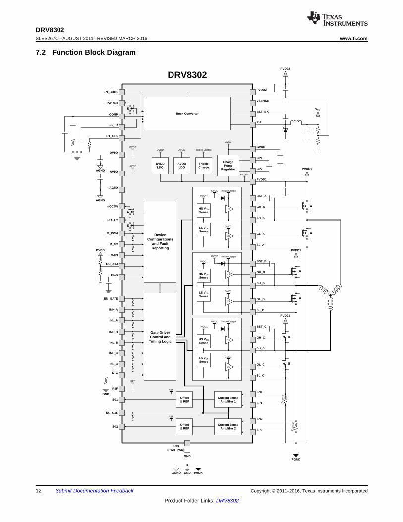
7.1 OverviewThe DRV8302 is a 8-V to 60-V, gate driver IC for three phase motor drive applications. This device reducesexternal component count by integrating three half-bridge drivers, two current shunt amplifiers, and a switchingbuck converter. The DRV8302 provides overcurrent, overtemperature, and undervoltage protection. Faultconditions are indicated through the nFAULT and nOCTW pins.
Adjustable dead time control allows for finely tuning the switching of the external MOSFETs. Internal handshaking is used to prevent shoot-through current. VDS sensing of the external MOSFETs allows for theDRV8302 to detect overcurrent conditions and respond appropriately. The VDS trip point can be set through ahardware pin.
The highly configurable buck converter can support a wide range of output options. This allows the DRV8302 toprovide a power supply rail for the controller and lower voltage components.
INH_A
GND (PWR_PAD)
nFAULT
Current Sense Amplifier 1
Current Sense Amplifier 2
GH_A
SH_A
GL_A
RIS
EN
SE
RIS
EN
SE
SL_A
GH_B
SH_B
GL_B
SL_B
GH_C
SH_C
GL_C
SL_C
SN1
SP1
SN2
SP2
BST_B
BST_A
BST_C
PVDD1
PVDD1
PVDD1
PGND
CP1
CP2
PVDD1
GVDD
GVDD
GVDD
GVDD
GVDD
Trickle Charge
Trickle Charge
Trickle Charge
Trickle Charge
Trickle Charge
GVDD
GVDD
GVDD
HS VDS
Sense
LS VDS
Sense
PVDD1
HS
LS
HS
LS
HS
LS
PVDD1
HS VDS
Sense
LS VDS
Sense
PVDD1
HS VDS
Sense
LS VDS
Sense
PVDD1
INL_A
INH_B
INL_B
INH_C
INL_C
DTC
nOCTW
EN_GATE
M_PWM
M_OC
GAIN
OC_ADJ
BIAS
Device Configurations
and Fault Reporting
Gate Driver Control and
Timing Logic
AVDD LDO
DVDD LDO
AVDDDVDDDVDD
AVDD
GND
AGND
AGND
Offset½ REF
REF
REF
Offset½ REF
REF
REF
SO1
SO2
DC_CAL
GND
GND PGNDAGND
Buck Converter
PVDD2
VSENSE
BST_BK
PH
PVDD2
VCC
DVDD
AVDD
AGND
EN_BUCK
PWRGD
SS_TR
RT_CLK
COMP
DRV8302
Charge Pump
Regulator
DVDD
12
DRV8302SLES267C –AUGUST 2011–REVISED MARCH 2016 www.ti.com
Product Folder Links: DRV8302
Submit Documentation Feedback Copyright © 2011–2016, Texas Instruments Incorporated
7.2 Function Block Diagram
13
DRV8302www.ti.com SLES267C –AUGUST 2011–REVISED MARCH 2016
Product Folder Links: DRV8302
Submit Documentation FeedbackCopyright © 2011–2016, Texas Instruments Incorporated
7.3 Feature Description
7.3.1 Three-Phase Gate DriverThe half-bridge drivers use a bootstrap configuration with a trickle charge pump to support 100% duty cycleoperation. Each half-bridge is configured to drive two N-channel MOSFETs, one for the high-side and one for thelow-side. The half-bridge drivers can be used in combination to drive a 3-phase motor or separately to drivevarious other loads.
The internal dead times are adjustable to accommodate a variety of external MOSFETs and applications. Thedead time is adjusted with an external resistor on the DTC pin. Shorting the DTC pin to ground provides theminimum dead time (50 ns). There is an internal hand shake between the high side and low side MOSFETsduring switching transitions to prevent current shoot-through.
The three-phase gate driver can provide up to 30 mA of average gate driver current. This can support switchingfrequencies up to 200 kHz when the MOSFET Qg = 25 nC. The high side gate drive will survive negative outputfrom the half-bridge up to –10 V for 10 ns. During EN_GATE low and fault conditions the gate driver keeps theexternal MOSFETs in high impedance mode.
Each MOSFET gate driver has a VDS sensing circuit for overcurrent protection. The sense circuit measures thevoltage from the drain to the source of the external MOSFETs while the MOSFET is enabled. This voltage iscompared against the programmed trip point to determine if an overcurrent event has occurred. The trip voltageis set through the OC_ADJ pin with a voltage usually set with a resistor divider. The high-side sense is betweenthe PVDD1 and SH_X pins. The low-side sense is between the SH_X and SL_X pins. Ensuring a differential, lowimpedance connection to the external MOSFETs for these lines helps provide accurate VDS sensing. TheDRV8302 provides both cycle-by-cycle current limiting and latch overcurrent shutdown of the external MOSFETthrough the M_OC pin.
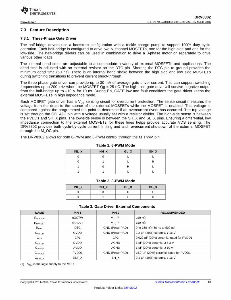
The DRV8302 allows for both 6-PWM and 3-PWM control through the M_PWM pin.
Table 1. 6-PWM ModeINL_X INH_X GL_X GH_X
0 0 L L0 1 L H1 0 H L1 1 L L
Table 2. 3-PWM ModeINL_X INH_X GL_X GH_X
X 0 H LX 1 L H
(1) VCC is the logic supply to the MCU
Table 3. Gate Driver External ComponentsNAME PIN 1 PIN 2 RECOMMENDEDRnOCTW nOCTW VCC
(1) ≥10 kΩRnFAULT nFAULT VCC
(1) ≥10 kΩRDTC DTC GND (PowerPAD) 0 to 150 kΩ (50 ns to 500 ns)
CGVDD GVDD GND (PowerPAD) 2.2 µF (20%) ceramic, ≥ 16 VCCP CP1 CP2 0.022 µF (20%) ceramic, rated for PVDD1
CDVDD DVDD AGND 1 µF (20%) ceramic, ≥ 6.3 VCAVDD AVDD AGND 1 µF (20%) ceramic, ≥ 10 VCPVDD1 PVDD1 GND (PowerPAD) ≥4.7 µF (20%) ceramic, rated for PVDD1CBST_X BST_X SH_X 0.1 µF (20%) ceramic, ≥ 16 V
SN
SP
SO
_
+
DC_CAL
DC_CAL
DC_CAL
S1
S2
S1
S2
5 kW
100 W
_
+
REF
Vref/2
AVDD
AVDD
200 kW
50 kW
5 kW
50 kW
200 kW
50 kW
50 kW
( )- ´ -REFO X X
VV = G SN SP
2
14
DRV8302SLES267C –AUGUST 2011–REVISED MARCH 2016 www.ti.com
Product Folder Links: DRV8302
Submit Documentation Feedback Copyright © 2011–2016, Texas Instruments Incorporated
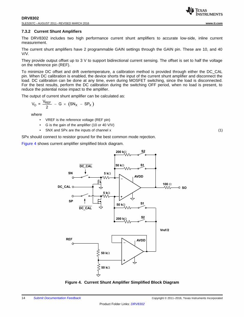
7.3.2 Current Shunt AmplifiersThe DRV8302 includes two high performance current shunt amplifiers to accurate low-side, inline currentmeasurement.
The current shunt amplifiers have 2 programmable GAIN settings through the GAIN pin. These are 10, and 40V/V.
They provide output offset up to 3 V to support bidirectional current sensing. The offset is set to half the voltageon the reference pin (REF).
To minimize DC offset and drift overtemperature, a calibration method is provided through either the DC_CALpin. When DC calibration is enabled, the device shorts the input of the current shunt amplifier and disconnect theload. DC calibration can be done at any time, even during MOSFET switching, since the load is disconnected.For the best results, perform the DC calibration during the switching OFF period, when no load is present, toreduce the potential noise impact to the amplifier.
The output of current shunt amplifier can be calculated as:
where• VREF is the reference voltage (REF pin)• G is the gain of the amplifier (10 or 40 V/V)• SNX and SPx are the inputs of channel x (1)
SPx should connect to resistor ground for the best common mode rejection.
Figure 4 shows current amplifier simplified block diagram.
Figure 4. Current Shunt Amplifier Simplified Block Diagram
15
DRV8302www.ti.com SLES267C –AUGUST 2011–REVISED MARCH 2016
Product Folder Links: DRV8302
Submit Documentation FeedbackCopyright © 2011–2016, Texas Instruments Incorporated
7.3.3 Buck ConverterThe DRV8302 uses an integrated TPS54160 1.5-A, 60-V, step-down DC-DC converter. Although integrated inthe same device, the buck converter is designed completely independent of the rest of the gate driver circuitry.Because the buck converter can support external MCU or other external power need, the independency of buckoperation is crucial for a reliable system; this gives the buck converter minimum impact from gate driveroperations. Some examples are: when gate driver shuts down due to any failure, the buck still operates unlessthe fault is coming from the buck itself. The buck keeps operating at much lower PVDD of 3.5 V, assuring thesystem has a smooth power-up and power-down sequence when gate driver is not able to operate due to a lowPVDD.
For proper selection of the buck converter external components, see the data sheet, TPS54160 1.5-A, 60-V,Step-Down DC/DC Converter With Eco-mode™, SLVSB56.
The buck has an integrated high-side N-channel MOSFET. To improve performance during line and loadtransients the device implements a constant frequency, current mode control which reduces output capacitanceand simplifies external frequency compensation design.
The wide switching frequency of 300 kHz to 2200 kHz allows for efficiency and size optimization when selectingthe output filter components. The switching frequency is adjusted using a resistor to ground on the RT_CLK pin.The device has an internal phase lock loop (PLL) on the RT_CLK pin that is used to synchronize the powerswitch turn on to a falling edge of an external system clock.
The buck converter has a default start-up voltage of approximately 2.5 V. The EN_BUCK pin has an internalpullup current source that can be used to adjust the input voltage undervoltage lockout (UVLO) threshold withtwo external resistors. In addition, the pullup current provides a default condition. When the EN_BUCK pin isfloating the device will operate. The operating current is 116 µA when not switching and under no load. When thedevice is disabled, the supply current is 1.3 µA.
The integrated 200-mΩ high-side MOSFET allows for high-efficiency power supply designs capable of delivering1.5 A of continuous current to a load. The bias voltage for the integrated high side MOSFET is supplied by acapacitor on the BOOT to PH pin. The boot capacitor voltage is monitored by an UVLO circuit that turns the highside MOSFET off when the boot voltage falls below a preset threshold. The buck can operate at high duty cyclesbecause of the boot UVLO. The output voltage can be stepped down to as low as the 0.8-V reference.
The BUCK has a power good comparator (PWRGD) which asserts when the regulated output voltage is lessthan 92% or greater than 109% of the nominal output voltage. The PWRGD pin is an open-drain output thatdeasserts when the VSENSE pin voltage is between 94% and 107% of the nominal output voltage, allowing thepin to transition high when a pullup resistor is used.
The BUCK minimizes excessive output overvoltage (OV) transients by taking advantage of the OV power goodcomparator. When the OV comparator is activated, the high-side MOSFET is turned off and masked from turningon until the output voltage is lower than 107%.
The SS_TR (slow start/tracking) pin is used to minimize inrush currents or provide power supply sequencingduring power-up. A small value capacitor should be coupled to the pin to adjust the slow start time. A resistordivider can be coupled to the pin for critical power supply sequencing requirements. The SS_TR pin isdischarged before the output powers up. This discharging ensures a repeatable restart after an overtemperaturefault,
The BUCK, also, discharges the slow-start capacitor during overload conditions with an overload recovery circuit.The overload recovery circuit slow-starts the output from the fault voltage to the nominal regulation voltage oncea fault condition is removed. A frequency foldback circuit reduces the switching frequency during start-up andovercurrent fault conditions to help control the inductor current.
DS DS DS(on)V I R= ´
16
DRV8302SLES267C –AUGUST 2011–REVISED MARCH 2016 www.ti.com
Product Folder Links: DRV8302
Submit Documentation Feedback Copyright © 2011–2016, Texas Instruments Incorporated
(1) VCC is the logic supply to the MCU
Table 4. Buck Regulator External ComponentsNAME PIN 1 PIN 2 RECOMMENDED
RRT_CLK RT_CLK GND (PowerPAD) See Buck ConverterCCOMP COMP GND (PowerPAD) See Buck Converter
RCCOMP COMP GND (PowerPAD) See Buck ConverterRVSENSE1 PH (Filtered) VSENSE See Buck ConverterRVSENSE2 VSENSE GND (PowerPAD) See Buck ConverterRPWRGD PWRGD VCC
(1) ≥ 10 kΩLPH PH PH (Filtered) See Buck ConverterDPH PH GND (PowerPAD) See Buck ConverterCPH PH (Filtered) GND (PowerPAD) See Buck Converter
CBST_BK BST_BK PH See Buck ConverterCPVDD2 PVDD2 GND (PowerPAD) ≥4.7 µF (20%) ceramic, rated for PVDD2CSS_TR SS_TR GND (PowerPAD) See Buck Converter
7.3.4 Protection FeaturesThe DRV8302 provides a broad range of protection features and fault condition reporting. The DRV8302 hasundervoltage and overtemperature protection for the IC. It also has overcurrent and undervoltage protection forthe MOSFET power stage. In fault shut down conditions all gate driver outputs is held low to ensure the externalMOSFETs are in a high impedance state.
7.3.4.1 Overcurrent Protection (OCP) and ReportingTo protect the power stage from damage due to excessive currents, VDS sensing circuitry is implemented in theDRV8302. Based on the RDS(on) of the external MOSFETs and the maximum allowed IDS, a voltage threshold canbe determined to trigger the overcurrent protection features when exceeded. The voltage threshold isprogrammed through the OC_ADJ pin by applying an external reference voltage with a DAC or resistor dividerfrom DVDD. Overcurrent protection should be used as a protection scheme only; it is not intended as a precisecurrent regulation scheme. There can be up to a 20% tolerance across channels for the VDS trip point.
(2)
The VDS sense circuit measures the voltage from the drain to the source of the external MOSFET while theMOSFET is enabled. The high-side sense is between the PVDD and SH_X pins. The low-side sense is betweenthe SH_X and SL_X pins. Ensuring a differential, low impedance connection to the external MOSFETs for theselines helps provide accurate VDS sensing.
There are two different overcurrent modes that can be set through the M_OC pin.
7.3.4.1.1 Current Limit Mode (M_OC = LOW)
In current limit mode the devices uses current limiting instead of device shutdown during an overcurrent event.After the overcurrent event, the MOSFET in which the overcurrent was detected in will shut off until the nextPWM cycle. The overcurrent event will be reported through the nOCTW pin. The nOCTW pin will be held low fora maximum 64 µs period (internal timer) or until the next PWM cycle. If another overcurrent event is triggeredfrom another MOSFET, during a previous overcurrent event, the reporting will continue for another 64 µs period(internal timer will restart) or until both PWM signals cycle.
In current limit mode the device uses current limiting instead of device shutdown during an overcurrent event. Inthis mode the device reports overcurrent events through the nOCTW pin. The nOCTW pin will be held low for amaximum 64 µs period (internal timer) or until the next PWM cycle. If another overcurrent event is triggered fromanother MOSFET, during a previous overcurrent event, the reporting will continue for another 64 µs period(internal timer will restart) or until both PWM signals cycle.
R1
R2
VOC
DVDD
OC_ADJ
DSOC
DS(on)
VI =
R
´ DS
R2DVDD = V
(R1 + R2)
17
DRV8302www.ti.com SLES267C –AUGUST 2011–REVISED MARCH 2016
Product Folder Links: DRV8302
Submit Documentation FeedbackCopyright © 2011–2016, Texas Instruments Incorporated
7.3.4.1.2 OC Latch Shutdown Mode
When an overcurrent event occurs, both the high-side and low-side MOSFETs will be disabled in thecorresponding half-bridge. The nFAULT pin will latch until the fault is reset through a quick EN_GATE resetpulse.
7.3.4.2 OC_ADJWhen external MOSFET is turned on, the output current flows through the on resistance, RDS(on) of the MOSFET,which creates a voltage drop VDS. The over current protection event will be enabled when the VDS exceeds a pre-set value. The voltage on OC_ADJ pin will be used to pre-set the OC tripped value. The OC tripped value IOChas to meet following equations:
where• R1 + R2 ≥ 1 KΩ• DVDD = 3.3 V (3)
(4)
Connect OC_ADJ pin to DVDD to disable the over-current protection feature.
Figure 5. OC_ADJ Current Programming Pin Connection
7.3.4.3 Undervoltage Protection (UVLO)To protect the power output stage during start-up, shutdown, and other possible undervoltage conditions, theDRV8302 provides undervoltage protection by driving the gate drive outputs (GH_X, GL_X) low whenever PVDDor GVDD are below their undervoltage thresholds (PVDD_UV/GVDD_UV). This will put the external MOSFETs ina high impedance state.
A specific PVDD1 undervoltage transient brownout from 13 to 15 µs can cause the DRV8302 to becomeunresponsive to external inputs until a full power cycle. The transient condition consists of having PVDD1 greaterthan the PVDD_UV level and then PVDD1 dropping below the PVDD_UV level for a specific period of 13 to 15µs. Transients shorter or longer than 13 to 15 µs will not affect the normal operation of the undervoltageprotection. Additional bulk capacitance can be added to PVDD1 to reduce undervoltage transients.
7.3.4.4 Overvoltage Protection (GVDD_OV)The device will shut down both the gate driver and charge pump if the GVDD voltage exceeds the GVDD_OVthreshold to prevent potential issues related to the GVDD pin or the charge pump (For example, short of externalGVDD cap or charge pump). The fault is a latched fault and can only be reset through a reset transition on theEN_GATE pin.
18
DRV8302SLES267C –AUGUST 2011–REVISED MARCH 2016 www.ti.com
Product Folder Links: DRV8302
Submit Documentation Feedback Copyright © 2011–2016, Texas Instruments Incorporated
7.3.4.5 Overtemperature ProtectionA two-level overtemperature detection circuit is implemented:• Level 1: overtemperature warning (OTW)
OTW is reported through nOCTW pin.• Level 2: overtemperature (OT) latched shut down of gate driver and charge pump (OTSD_GATE)
Fault will be reported to nFAULT pin. This is a latched shut down, so gate driver will not be recoveredautomatically even if OT condition is not present anymore. An EN_GATE reset through pin is required torecover gate driver to normal operation after temperature goes below a preset value, tOTSD_CLR.
7.3.4.6 Fault and Protection HandlingThe nFAULT pin indicates an error event with shut down has occurred such as over-current, overtemperature,overvoltage, or undervoltage. Note that nFAULT is an open-drain signal. nFAULT goes high when gate driver isready for PWM signal (internal EN_GATE goes high) during start-up.
The nOCTW pin indicates an overtemperature or over current event that is not necessarily related to shut down.
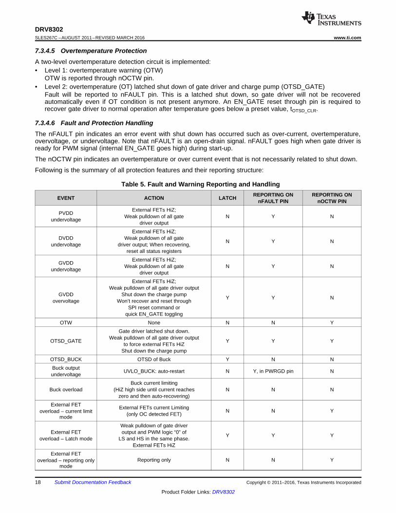
Following is the summary of all protection features and their reporting structure:
Table 5. Fault and Warning Reporting and Handling
EVENT ACTION LATCH REPORTING ONnFAULT PIN
REPORTING ONnOCTW PIN
PVDDundervoltage
External FETs HiZ;Weak pulldown of all gate
driver outputN Y N
DVDDundervoltage
External FETs HiZ;Weak pulldown of all gate
driver output; When recovering,reset all status registers
N Y N
GVDDundervoltage
External FETs HiZ;Weak pulldown of all gate
driver outputN Y N
GVDDovervoltage
External FETs HiZ;Weak pulldown of all gate driver output
Shut down the charge pumpWon’t recover and reset through
SPI reset command orquick EN_GATE toggling
Y Y N
OTW None N N Y
OTSD_GATE
Gate driver latched shut down.Weak pulldown of all gate driver output
to force external FETs HiZShut down the charge pump
Y Y Y
OTSD_BUCK OTSD of Buck Y N NBuck outputundervoltage UVLO_BUCK: auto-restart N Y, in PWRGD pin N
Buck overloadBuck current limiting
(HiZ high side until current reacheszero and then auto-recovering)
N N N
External FEToverload – current limit
mode
External FETs current Limiting(only OC detected FET) N N Y
External FEToverload – Latch mode
Weak pulldown of gate driveroutput and PWM logic “0” of
LS and HS in the same phase.External FETs HiZ
Y Y Y
External FEToverload – reporting only
modeReporting only N N Y

19
DRV8302www.ti.com SLES267C –AUGUST 2011–REVISED MARCH 2016
Product Folder Links: DRV8302
Submit Documentation FeedbackCopyright © 2011–2016, Texas Instruments Incorporated
7.4 Device Functional Modes
7.4.1 EN_GATEEN_GATE low is used to put gate driver, charge pump, current shunt amplifier, and internal regulator blocks intoa low-power consumption mode to save energy. The device will put the MOSFET output stage to high-impedance mode as long as PVDD is still present.
When the EN_GATE pin goes low to high, it goes through a power-up sequence, and enable gate driver, currentamplifiers, charge pump, internal regulator, and so forth and reset all latched faults related to gate driver block.All latched faults can be reset when EN_GATE is toggled after an error event unless the fault is still present.
When EN_GATE goes from high to low, it will shut down gate driver block immediately, so gate output can putexternal FETs in high impedance mode. It will then wait for 10 µs before completely shutting down the rest of theblocks. A quick fault reset mode can be done by toggling EN_GATE pin for a very short period (less than 10 µs).This will prevent the device from shutting down the other functional blocks such as charge pump and internalregulators and bring a quicker and simple fault recovery. To perform a full reset, EN_GATE should be toggled forlonger than 20 µs. This allows for all of the blocks to completely shut down and reach known states.
An EN_GATE reset pulse (high → low → high) from 10 to 20 µs should not be applied to the EN_GATE pin. TheDRV8301 has a transition area from the quick to full reset modes that can cause the device to becomeunresponsive to external inputs until a full power cycle. An RC filter can be added externally to the pin if resetpulses with this period are expected to occur on the EN_GATE pin.
One exception is to reset a GVDD_OV fault. A quick EN_GATE quick fault reset will not work with GVDD_OVfault. A complete EN_GATE with low level holding longer than 20 µs is required to reset GVDD_OV fault. TIhighly recommends inspecting the system and board when GVDD_OV occurs.
7.4.2 DTCDead time can be programmed through DTC pin. A resistor should be connected from DTC to ground to controlthe dead time. Dead time control range is from 50 ns to 500 ns. Short DTC pin to ground provides minimumdead time (50 ns). Resistor range is 0 to 150 kΩ. Dead time is linearly set over this resistor range. Current shoot-through prevention protection will be enabled in the device all time independent of dead time setting and inputmode setting.
20
DRV8302SLES267C –AUGUST 2011–REVISED MARCH 2016 www.ti.com
Product Folder Links: DRV8302
Submit Documentation Feedback Copyright © 2011–2016, Texas Instruments Incorporated
8 Application and Implementation
NOTEInformation in the following applications sections is not part of the TI componentspecification, and TI does not warrant its accuracy or completeness. TI’s customers areresponsible for determining suitability of components for their purposes. Customers shouldvalidate and test their design implementation to confirm system functionality.
8.1 Application InformationThe DRV8302 is a gate driver designed to drive a 3-phase BLDC motor in combination with external powerMOSFETs. The device provides a high level of integration with three half-bridge gate drivers, two current shuntamplifiers, overcurrent protection, and a step-down buck regulator.
8.1.1 Gate Driver Power Up Sequencing ErrdataThe DRV8301 gate drivers may not correctly power-up if a voltage greater than 8.5 V is present on any SH_Xpin when EN_GATE is brought logic high (device enabled) after PVDD1 power is applied (PVDD1 > PVDD_UV).This sequence should be avoided by ensuring the voltage levels on the SH_X pins are less than 8.5 V when theDRV8301 is enabled through EN_GATE.
RT_CLK1
2COMP
3VSENSE
4PWRGD
5nOCTW
6 nFAULT7
DTC8
M_PWM9
M_OC10
GAIN11
OC_ADJ12
DC_CAL13 GVDD14
CP115
CP216
EN_GATE17
INH_A18
INL_A19
INH_B20 INL_B21
INH_C22 INL_C23
DVDD24
REF25
SO126
SO227 AVDD28
AGND
SS_TR56
55EN_BUCK
54PVDD2
53PVDD2
52BST_BK
51PH50
PH49
BIAS48
BST_A47
GH_A46
SH_A45
GL_A44SL_A43
BST_B42
GH_B41
SH_B40
GL_B39
SL_B38
BST_C37GH_C36
SH_C35GL_C34
SL_C33
SN132
SP131
SN230SP229
PVDD1
57P
PA
D
GH_C
SH_C
GL_C
SL_C
GH_B
SH_B
GL_B
SL_B
GH_A
SH_A
GL_A
SL_A
SN1
SP1
SN2
SP2
0.1 µF
0.1 µF
0.1 µF
47 µ
F
GND PGNDAGND
VCC22 µH0.1 µF
PVDD
0.1
µF
4.7
µF
0.01
5 µ
F
PVDD
0.1
µF
4.7
µF
1 µF
1 µF
56
56
2200
pF
2200
pF
0.022 µF2.
2 µ
F
1
PVDDSENSE
ASENSE
BSENSE
CSENSE
MCU DRV8302
ADC
PWM
GPIO
DAC
GPIO
10 k
10 k
10 k
VCC
10 k
31.6
k 20
5 k
6800
pF
120
pF16.2
k
POWER
VCC
X
+
GPIO
1 M
10
10
PVDD
10
m
100
0 p
FSN1
SP1
GH_A
SH_A
GL_A
SL_A
2.2
µF
34.8
k
4.99
k
0.1
µF
AS
EN
SE
VCC
10
10
PVDD
10
m
100
0 p
FSN2
SP2
GH_B
SH_B
GL_B
SL_B
2.2
µF
34.8
k
4.99
k
0.1
µF
BS
EN
SE
VCC
10
10
PVDD
GH_B
SH_B
GL_B
SL_B
2.2
µF
34.8
k
4.99
k
0.1
µF
CS
EN
SE
VCC
Diff . Pair Diff . Pair
PVDD
220
µF
220
µF
0.1
µF
0.0
1 µ
F3.
3 34
.8 k
4.99
k
0.1
µF
PVDDSENSE
VCC
GND PGNDAGND
+ +
21
DRV8302www.ti.com SLES267C –AUGUST 2011–REVISED MARCH 2016
Product Folder Links: DRV8302
Submit Documentation FeedbackCopyright © 2011–2016, Texas Instruments Incorporated
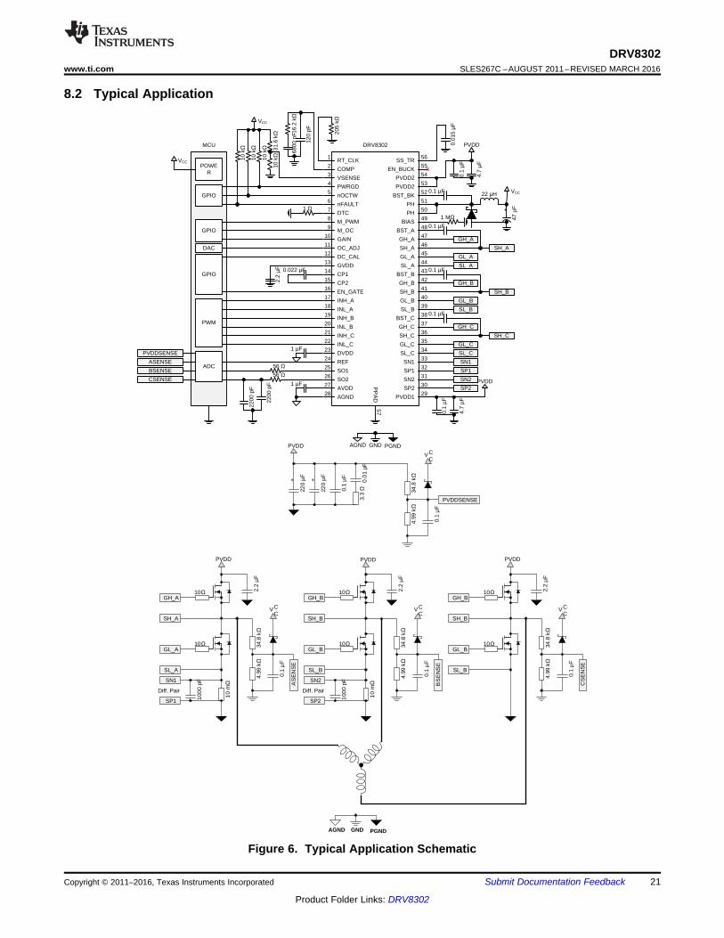
8.2 Typical Application
Figure 6. Typical Application Schematic
22
DRV8302SLES267C –AUGUST 2011–REVISED MARCH 2016 www.ti.com
Product Folder Links: DRV8302
Submit Documentation Feedback Copyright © 2011–2016, Texas Instruments Incorporated
Typical Application (continued)Example:Buck: PVDD = 3.5 V – 40 V, Iout_max = 1.5 A, Vo = 3.3 V, Fs = 570 kHz
8.2.1 Design Requirements
Table 6. Design ParametersDESIGN PARAMETER REFERENCE VALUE
Supply voltage PVDD 24 VMotor winding resistance MR 0.5 ΩMotor winding inductance ML 0.28 mHMotor poles MP 16 polesMotor rated RPM MRPM 4000 RPMTarget full-scale current IMAX 14 ASense resistor RSENSE 0.01 ΩMOSFET Qg Qg 29 nCMOSFET RDS(on) RDS(on) 4.7 mΩVDS trip level OC_ADJ_SET 0.123 VSwitching frequency ƒSW 45 kHzSeries gate resistance RGATE 10 ΩAmplifier reference VREF 3.3 VAmplifier gain Gain 10 V/V
8.2.2 Detailed Design Procedure
8.2.2.1 Gate Drive Average Current LoadThe gate drive supply (GVDD) of the DRV8302 can deliver up to 30 mA (RMS) of current to the external powerMOSFETs. Use Equation 5 to determine the approximate RMS load on the gate drive supply:
Gate Drive RMS Current = MOSFET Qg × Number of Switching MOSFETs × Switching Frequency (5)
Example:7.83 mA = 29 nC × 6 × 45 kHz (6)
This is a rough approximation only.
8.2.2.2 Overcurrent Protection SetupThe DRV8302 provides overcurrent protection for the external power MOSFETs through the use of VDSmonitors for both the high side and low side MOSFETs. These are intended for protecting the MOSFET inovercurrent conditions and not for precise current regulation.
The overcurrent protection works by monitoring the VDS voltage of the external MOSFET and comparing itagainst the OC_ADJ pin voltage. If the VDS exceeds the OC_ADJ pin voltage the DRV8302 takes actionaccording to the M_OC pin.
Overcurrent Trip = OC_ADJ_SET / MOSFET RDS(on) (7)
Example:26.17 A = 0.123 V/ 4.7 mΩ (8)
MOSFET RDS(on) changes with temperature and this will affect the overcurrent trip level.
8.2.2.3 Sense Amplifier SetupThe DRV8302 provides two bidirectional low-side current shunt amplifiers. These can be used to sense a sum ofthe three half-bridges, two of the half-bridges individually, or in conjunction with an additional shunt amplifier tosense all three half-bridges individually.1. Determine the peak current that the motor will demand (IMAX). This will be dependent on the motor
23
DRV8302www.ti.com SLES267C –AUGUST 2011–REVISED MARCH 2016
Product Folder Links: DRV8302
Submit Documentation FeedbackCopyright © 2011–2016, Texas Instruments Incorporated
parameters and your specific application. I(MAX) in this example is 14 A.2. Determine the available voltage range for the current shunt amplifier. This will be ± half of the amplifier
reference voltage (VREF). In this case the available range is ±1.65 V.3. Determine the sense resistor value and amplifier gain settings. There are common tradeoffs for both the
sense resistor value and amplifier gain. The larger the sense resistor value, the better the resolution of thehalf-bridge current. This comes at the cost of additional power dissipated from the sense resistor. A largergain value will allow you to decrease the sense resistor, but at the cost of increased noise in the outputsignal. This example uses a 0.01-Ω sense resistor and the minimum gain setting of the DRV8302 (10 V/V).These values allow the current shunt amplifiers to measure ±16.5 A (some additional margin on the 14-Arequirement).
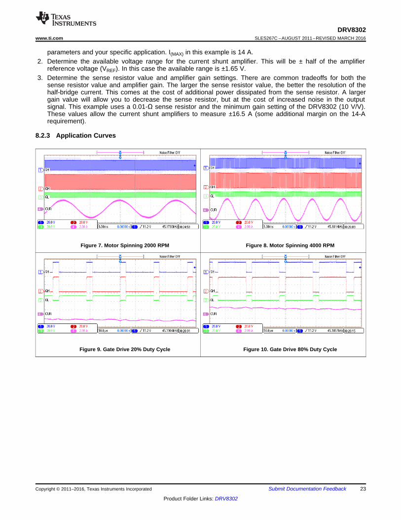
8.2.3 Application Curves
Figure 7. Motor Spinning 2000 RPM Figure 8. Motor Spinning 4000 RPM
Figure 9. Gate Drive 20% Duty Cycle Figure 10. Gate Drive 80% Duty Cycle
Local
Bulk Capacitor
Parasitic Wire
Inductance
+–
Motor
Driver
Power Supply Motor Drive System
VM
GND
+
IC Bypass
Capacitor
24
DRV8302SLES267C –AUGUST 2011–REVISED MARCH 2016 www.ti.com
Product Folder Links: DRV8302
Submit Documentation Feedback Copyright © 2011–2016, Texas Instruments Incorporated
9 Power Supply Recommendations
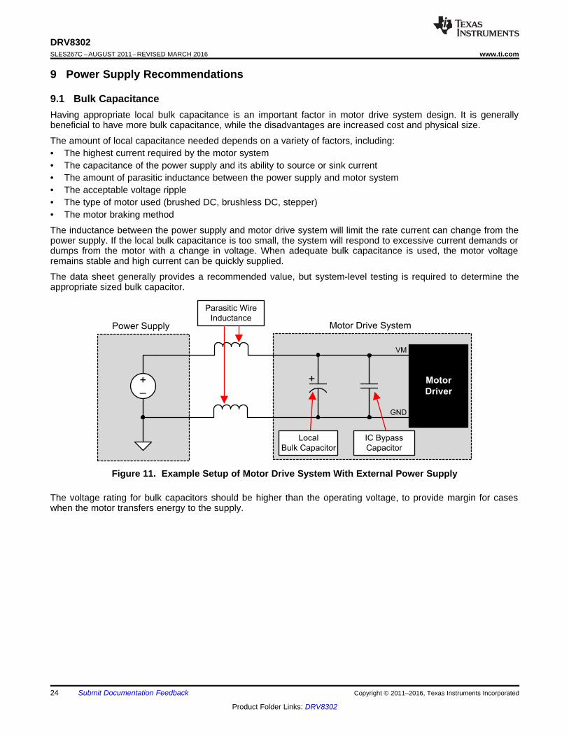
9.1 Bulk CapacitanceHaving appropriate local bulk capacitance is an important factor in motor drive system design. It is generallybeneficial to have more bulk capacitance, while the disadvantages are increased cost and physical size.
The amount of local capacitance needed depends on a variety of factors, including:• The highest current required by the motor system• The capacitance of the power supply and its ability to source or sink current• The amount of parasitic inductance between the power supply and motor system• The acceptable voltage ripple• The type of motor used (brushed DC, brushless DC, stepper)• The motor braking method
The inductance between the power supply and motor drive system will limit the rate current can change from thepower supply. If the local bulk capacitance is too small, the system will respond to excessive current demands ordumps from the motor with a change in voltage. When adequate bulk capacitance is used, the motor voltageremains stable and high current can be quickly supplied.
The data sheet generally provides a recommended value, but system-level testing is required to determine theappropriate sized bulk capacitor.
Figure 11. Example Setup of Motor Drive System With External Power Supply
The voltage rating for bulk capacitors should be higher than the operating voltage, to provide margin for caseswhen the motor transfers energy to the supply.
1RT_CLK
Pow
er P
ad (
57)
- G
ND
2
3
4
12
5
6
7
8
9
10
11
13
14
15
16
17
18
26
19
20
21
22
23
24
25
27
28
56
55
54
53
45
52
51
50
49
48
47
46
44
43
42
41
40
39
31
38
37
36
35
34
33
32
30
29
COMPVSENSEPWRGDnOCTWnFAULT
DTCM_PWM
M_OC
DC_CAL
GAINOC_ADJ
GVDDCP1CP2
EN_GATEINH_AINL_AINH_BINL_BINH_CINL_CDVDD
REFSO1SO2
AVDDAGND
SS_TREN_BUCKPVDD2PVDD2BST_BKPHPHBIASBST_A
GL_A
GH_ASH_A
SL_ABST_BGH_BSH_BGL_BSL_BBST_CGH_CSH_CGL_CSL_CSN1SP1SN2SP2PVDD1
0.1 µF
0.1 µF
0.1 µF
0.1 µF
0.1 µF4.7 µF
0.1 µF4.7 µF
Top Layer
Bottom Layer
10
D
D
D
D
G
S
S
S
D
D
D
D
G
S
S
S
D
D
D
D
G
S
S
S
D
D
D
D
G
S
S
S
D
D
D
D
G
S
S
S
D
D
D
D
G
S
S
S
OUTA
OUTB
OUTC
10
10
10
10
10
220 µF
220 µF
10 m
10 m
PVDDGND
2.2 µF
2.2 µF
2.2 µF
1000 pF
1000 pF
47 µF
22 µH
0.015 µF
VCC
Via
Legend
1 µF
1 µF
0.022 µF
0.1 µF
GND
GND
GND
GND
GN
D
1
31.6
k
10 k
6800
pF
16.2
k
120
pF
VCC
10 k
1 M
25
DRV8302www.ti.com SLES267C –AUGUST 2011–REVISED MARCH 2016
Product Folder Links: DRV8302
Submit Documentation FeedbackCopyright © 2011–2016, Texas Instruments Incorporated
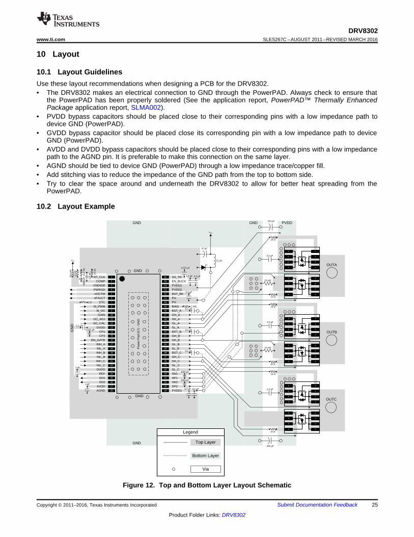
10 Layout
10.1 Layout GuidelinesUse these layout recommendations when designing a PCB for the DRV8302.• The DRV8302 makes an electrical connection to GND through the PowerPAD. Always check to ensure that
the PowerPAD has been properly soldered (See the application report, PowerPAD™ Thermally EnhancedPackage application report, SLMA002).
• PVDD bypass capacitors should be placed close to their corresponding pins with a low impedance path todevice GND (PowerPAD).
• GVDD bypass capacitor should be placed close its corresponding pin with a low impedance path to deviceGND (PowerPAD).
• AVDD and DVDD bypass capacitors should be placed close to their corresponding pins with a low impedancepath to the AGND pin. It is preferable to make this connection on the same layer.
• AGND should be tied to device GND (PowerPAD) through a low impedance trace/copper fill.• Add stitching vias to reduce the impedance of the GND path from the top to bottom side.• Try to clear the space around and underneath the DRV8302 to allow for better heat spreading from the
PowerPAD.
10.2 Layout Example
Figure 12. Top and Bottom Layer Layout Schematic

26
DRV8302SLES267C –AUGUST 2011–REVISED MARCH 2016 www.ti.com
Product Folder Links: DRV8302
Submit Documentation Feedback Copyright © 2011–2016, Texas Instruments Incorporated
11 Device and Documentation Support
11.1 Documentation Support
11.1.1 Related DocumentationFor related documentation, see the following:• PowerPAD Thermally Enhanced Package, SLMA002• TPS54160 1.5-A, 60-V, Step-Down DC/DC Converter With Eco-mode™, SLVSB56
11.2 Community ResourcesThe following links connect to TI community resources. Linked contents are provided "AS IS" by the respectivecontributors. They do not constitute TI specifications and do not necessarily reflect TI's views; see TI's Terms ofUse.
TI E2E™ Online Community TI's Engineer-to-Engineer (E2E) Community. Created to foster collaborationamong engineers. At e2e.ti.com, you can ask questions, share knowledge, explore ideas and helpsolve problems with fellow engineers.
Design Support TI's Design Support Quickly find helpful E2E forums along with design support tools andcontact information for technical support.
11.3 TrademarksPowerPAD, E2E are trademarks of Texas Instruments.All other trademarks are the property of their respective owners.
11.4 Electrostatic Discharge CautionThese devices have limited built-in ESD protection. The leads should be shorted together or the device placed in conductive foamduring storage or handling to prevent electrostatic damage to the MOS gates.
11.5 GlossarySLYZ022 — TI Glossary.
This glossary lists and explains terms, acronyms, and definitions.
12 Mechanical, Packaging, and Orderable InformationThe following pages include mechanical, packaging, and orderable information. This information is the mostcurrent data available for the designated devices. This data is subject to change without notice and revision ofthis document. For browser-based versions of this data sheet, refer to the left-hand navigation.
PACKAGE OPTION ADDENDUM
www.ti.com 1-Mar-2016
Addendum-Page 1
PACKAGING INFORMATION
Orderable Device Status(1)
Package Type PackageDrawing
Pins PackageQty
Eco Plan(2)
Lead/Ball Finish(6)
MSL Peak Temp(3)
Op Temp (°C) Device Marking(4/5)
Samples
DRV8302DCA ACTIVE HTSSOP DCA 56 35 Green (RoHS& no Sb/Br)
CU NIPDAU Level-3-260C-168 HR -40 to 125 DRV8302
DRV8302DCAR ACTIVE HTSSOP DCA 56 2000 Green (RoHS& no Sb/Br)
CU NIPDAU Level-3-260C-168 HR -40 to 125 DRV8302
(1) The marketing status values are defined as follows:ACTIVE: Product device recommended for new designs.LIFEBUY: TI has announced that the device will be discontinued, and a lifetime-buy period is in effect.NRND: Not recommended for new designs. Device is in production to support existing customers, but TI does not recommend using this part in a new design.PREVIEW: Device has been announced but is not in production. Samples may or may not be available.OBSOLETE: TI has discontinued the production of the device.
(2) Eco Plan - The planned eco-friendly classification: Pb-Free (RoHS), Pb-Free (RoHS Exempt), or Green (RoHS & no Sb/Br) - please check http://www.ti.com/productcontent for the latest availabilityinformation and additional product content details.TBD: The Pb-Free/Green conversion plan has not been defined.Pb-Free (RoHS): TI's terms "Lead-Free" or "Pb-Free" mean semiconductor products that are compatible with the current RoHS requirements for all 6 substances, including the requirement thatlead not exceed 0.1% by weight in homogeneous materials. Where designed to be soldered at high temperatures, TI Pb-Free products are suitable for use in specified lead-free processes.Pb-Free (RoHS Exempt): This component has a RoHS exemption for either 1) lead-based flip-chip solder bumps used between the die and package, or 2) lead-based die adhesive used betweenthe die and leadframe. The component is otherwise considered Pb-Free (RoHS compatible) as defined above.Green (RoHS & no Sb/Br): TI defines "Green" to mean Pb-Free (RoHS compatible), and free of Bromine (Br) and Antimony (Sb) based flame retardants (Br or Sb do not exceed 0.1% by weightin homogeneous material)
(3) MSL, Peak Temp. - The Moisture Sensitivity Level rating according to the JEDEC industry standard classifications, and peak solder temperature.
(4) There may be additional marking, which relates to the logo, the lot trace code information, or the environmental category on the device.
(5) Multiple Device Markings will be inside parentheses. Only one Device Marking contained in parentheses and separated by a "~" will appear on a device. If a line is indented then it is a continuationof the previous line and the two combined represent the entire Device Marking for that device.
(6) Lead/Ball Finish - Orderable Devices may have multiple material finish options. Finish options are separated by a vertical ruled line. Lead/Ball Finish values may wrap to two lines if the finishvalue exceeds the maximum column width.
Important Information and Disclaimer:The information provided on this page represents TI's knowledge and belief as of the date that it is provided. TI bases its knowledge and belief on informationprovided by third parties, and makes no representation or warranty as to the accuracy of such information. Efforts are underway to better integrate information from third parties. TI has taken andcontinues to take reasonable steps to provide representative and accurate information but may not have conducted destructive testing or chemical analysis on incoming materials and chemicals.TI and TI suppliers consider certain information to be proprietary, and thus CAS numbers and other limited information may not be available for release.
PACKAGE OPTION ADDENDUM
www.ti.com 1-Mar-2016
Addendum-Page 2
In no event shall TI's liability arising out of such information exceed the total purchase price of the TI part(s) at issue in this document sold by TI to Customer on an annual basis.
IMPORTANT NOTICE
Texas Instruments Incorporated and its subsidiaries (TI) reserve the right to make corrections, enhancements, improvements and otherchanges to its semiconductor products and services per JESD46, latest issue, and to discontinue any product or service per JESD48, latestissue. Buyers should obtain the latest relevant information before placing orders and should verify that such information is current andcomplete. All semiconductor products (also referred to herein as “components”) are sold subject to TI’s terms and conditions of salesupplied at the time of order acknowledgment.TI warrants performance of its components to the specifications applicable at the time of sale, in accordance with the warranty in TI’s termsand conditions of sale of semiconductor products. Testing and other quality control techniques are used to the extent TI deems necessaryto support this warranty. Except where mandated by applicable law, testing of all parameters of each component is not necessarilyperformed.TI assumes no liability for applications assistance or the design of Buyers’ products. Buyers are responsible for their products andapplications using TI components. To minimize the risks associated with Buyers’ products and applications, Buyers should provideadequate design and operating safeguards.TI does not warrant or represent that any license, either express or implied, is granted under any patent right, copyright, mask work right, orother intellectual property right relating to any combination, machine, or process in which TI components or services are used. Informationpublished by TI regarding third-party products or services does not constitute a license to use such products or services or a warranty orendorsement thereof. Use of such information may require a license from a third party under the patents or other intellectual property of thethird party, or a license from TI under the patents or other intellectual property of TI.Reproduction of significant portions of TI information in TI data books or data sheets is permissible only if reproduction is without alterationand is accompanied by all associated warranties, conditions, limitations, and notices. TI is not responsible or liable for such altereddocumentation. Information of third parties may be subject to additional restrictions.Resale of TI components or services with statements different from or beyond the parameters stated by TI for that component or servicevoids all express and any implied warranties for the associated TI component or service and is an unfair and deceptive business practice.TI is not responsible or liable for any such statements.Buyer acknowledges and agrees that it is solely responsible for compliance with all legal, regulatory and safety-related requirementsconcerning its products, and any use of TI components in its applications, notwithstanding any applications-related information or supportthat may be provided by TI. Buyer represents and agrees that it has all the necessary expertise to create and implement safeguards whichanticipate dangerous consequences of failures, monitor failures and their consequences, lessen the likelihood of failures that might causeharm and take appropriate remedial actions. Buyer will fully indemnify TI and its representatives against any damages arising out of the useof any TI components in safety-critical applications.In some cases, TI components may be promoted specifically to facilitate safety-related applications. With such components, TI’s goal is tohelp enable customers to design and create their own end-product solutions that meet applicable functional safety standards andrequirements. Nonetheless, such components are subject to these terms.No TI components are authorized for use in FDA Class III (or similar life-critical medical equipment) unless authorized officers of the partieshave executed a special agreement specifically governing such use.Only those TI components which TI has specifically designated as military grade or “enhanced plastic” are designed and intended for use inmilitary/aerospace applications or environments. Buyer acknowledges and agrees that any military or aerospace use of TI componentswhich have not been so designated is solely at the Buyer's risk, and that Buyer is solely responsible for compliance with all legal andregulatory requirements in connection with such use.TI has specifically designated certain components as meeting ISO/TS16949 requirements, mainly for automotive use. In any case of use ofnon-designated products, TI will not be responsible for any failure to meet ISO/TS16949.
Products ApplicationsAudio www.ti.com/audio Automotive and Transportation www.ti.com/automotiveAmplifiers amplifier.ti.com Communications and Telecom www.ti.com/communicationsData Converters dataconverter.ti.com Computers and Peripherals www.ti.com/computersDLP® Products www.dlp.com Consumer Electronics www.ti.com/consumer-appsDSP dsp.ti.com Energy and Lighting www.ti.com/energyClocks and Timers www.ti.com/clocks Industrial www.ti.com/industrialInterface interface.ti.com Medical www.ti.com/medicalLogic logic.ti.com Security www.ti.com/securityPower Mgmt power.ti.com Space, Avionics and Defense www.ti.com/space-avionics-defenseMicrocontrollers microcontroller.ti.com Video and Imaging www.ti.com/videoRFID www.ti-rfid.comOMAP Applications Processors www.ti.com/omap TI E2E Community e2e.ti.comWireless Connectivity www.ti.com/wirelessconnectivity
Mailing Address: Texas Instruments, Post Office Box 655303, Dallas, Texas 75265Copyright © 2016, Texas Instruments Incorporated
Top Related