


Languages
Pages
Legal


©2012 Micron Technology, Inc. All rights reserved. Products are warranted only to meet Micron’s production data sheet specifications. Information, products, and/or specifications are subject to change without notice. All information is provided on an “AS IS” basis without warranties of any kind. Dates are estimates only. Drawings are not to scale. Micron and the Micron logo are trademarks of Micron Technology, Inc. All other trademarks are the property of their respective owners.
1 ©2012 Micron Technology, Inc. |
DRAM Memory
In High-Speed Digital Designs Presented by:
Micron – The Worlds Memory Expert & Agilent Partner
June 6, 2013

2 ©2012 Micron Technology, Inc. | June 6, 2013
Agenda
• Introduction
• Micron overview
• Choosing a memory in high-speed designs
• Micron Memory portfolio and segments
• DRAM volume drivers
• Evolution of DDR, introducing DDR4
• General DRAM design considerations
• General layout and termination
• SSO – Simultaneous Switching outputs
• RPD – Return Path Discontinuities
• ISI – Intersymbol Interference
• Crosstalk
• Vref
•Pathlength, Cin and Rtt

3 ©2012 Micron Technology, Inc. | June 6, 2013

4 ©2012 Micron Technology, Inc. | June 6, 2013
Why is Memory important in High-Speed Digital designs?
• Applications demand specific memory features - Memory
now plays a vital role in system performance
• Speed? Bandwidth? Power? Latency? Density?
• Memory is no longer just commoditized & standardized -
Making the right memory decisions is critical
• SDR, DDR 1 / 2 / 3(3L) / 4, HMC?
• Format (component or module type)?
• Price, availability & quality?

5 ©2012 Micron Technology, Inc. |
Micron supplies the right Memory…….
Parallel NOR Serial NOR
Client SSD Enterprise SATA Enterprise SAS Enterprise PCIe
TLC, MLC, SLC Serial NAND Enterprise NAND
Serial PCM Parallel PCM
SDRAM DDR DDR2 DDR3(3L) DDR4 RLDRAM® Mobile LPDRAM PSRAM/ CellularRAM HMC
FBDIMM RDIMM VLP RDIMM VLP UDIMM UDIMM SODIMM SORDIMM Mini-DIMM VLP Mini-DIMM LRDIMM NVDIMM
MCP eMMC™ Embedded USB
Multiple technologies
Solid State Drives
NOR Flash
NAND Flash
Phase Change Memory
DRAM Families DRAM Modules
Managed NAND
Bare Die
June 6, 2013

6 ©2012 Micron Technology, Inc. |
Automotive
Server Wireless Personal Computing Industrial
Storage Graphics / Consumer Networks
June 6, 2013
…for every Application.

7 Micron Confidential | ©2012 Micron Technology, Inc. |
DDR2/3(3L)/4 SDRAM Volume Drivers
Volume Drivers
DDR2 – 800MT/s (400MHz CLK), 1Gb and 2Gb
Backwards compatible with 400/533/667 speeds
DDR3L – 1600MT/s (800MHz CLK), 2Gb and 4Gb
Backwards compatible with 800/1066/1333 speeds
DDR4 – 2133MT/s (1066MHz CLK), 4Gb
Backwards compatible with 1600/1866 speeds
Power (IDD7/IPP7)
DDR2 – 396mW (50nm, 2Gb, 800MT/s)
DDR3L – 339mW (30nm, 4Gb, 1866MT/s)
DDR4 – 247mW (30nm, 4Gb, 1866MT/s)
June 6, 2013

8 Micron Confidential | ©2012 Micron Technology, Inc. |
DDR2/DDR3(3L)/DDR4 Feature Highlight (see background for full summary)
6/6/2013 8
Features/Options DDR2 DDR3(3L) DDR4
Voltage (core, /IO) 1.8V 1.5V 1.2V
Vref Inputs 1 – DQs/CMD/ADDR 2 – DQs and CMD/ADDR 1 –CMD/ADDR
VREFDQ Calibration none none Supported/Required
tCKbase – DLL enabled 125MHz to 400MHz 300MHz to 800MHz 625MHz to 1.6GHz
Data Rate - Mb/s 400/533/667/800
plus1066
800 /1066/1333/1600
plus1866, 2133
1600/1866/2133 /2400/
2667/3200
DQ Bus SSTL18 SSTL15 POD12
ODT Modes Nominal, Dynamic Nominal, Dynamic Nominal, Dynamic, Park
MultiPurpose Register None 1 Defined, 3 RFU 3 Defined, 1 RFU
VPP Supply none none 2.5V
Bank Group none none four
Data Bus Write CRC none none supported
Data Bus Inversion (DBI) none none supported
Connectivity Test Mode none none supported

9 Micron Confidential | ©2012 Micron Technology, Inc. |
Self Refresh (IDD6 with ASR, LPASR) Micron – Rs parts
June 6, 2013
DDR2 Range of Commercial Operation
DDR3, DDR4 Range of Commercial Operation
DD
R2 S
elf R
efr
esh
Range o
f O
pera
tion
DD
R3L S
elf R
efr
esh
Range o
f O
pera
tion
DD
R4 S
elf R
efr
esh
Range o
f O
pera
tion
0oC

10 Micron Confidential | ©2012 Micron Technology, Inc. |
DDR2/3(3L)/4 Implementation
June 6, 2013

©2012 Micron Technology, Inc. All rights reserved. Products are warranted only to meet Micron’s production data sheet specifications. Information, products, and/or specifications are subject to change without notice. All information is provided on an “AS IS” basis without warranties of any kind. Dates are estimates only. Drawings are not to scale. Micron and the Micron logo are trademarks of Micron Technology, Inc. All other trademarks are the property of their respective owners.
11 ©2012 Micron Technology, Inc. |
DRAM Appnotes on www.micron.com
June 6, 2013

12 Micron Confidential | ©2012 Micron Technology, Inc. |
General Layout Concerns
DLL added
Clock jitter increasingly important as speeds go up
Reduces data eye out by 2x the amount of jitter in
Avoid crossing splits in the power plane
Low pass VREF filtering on controller helps
Minimize Vref Noise
Minimize ISI
Minimize Crosstalk
June 6, 2013

13 Micron Confidential | ©2012 Micron Technology, Inc. |
Layout and Termination
Guidelines

14 Micron Confidential | ©2012 Micron Technology, Inc. |
“Near Perfect” Data-Eye

15 Micron Confidential | ©2012 Micron Technology, Inc. |
Unadjusted, Non-terminated Data-Eye
Jitter
Overshoot
Undershoot
VDD
VSS

16 Micron Confidential | ©2012 Micron Technology, Inc. |
Terminated Data-Eye
VIHac
VILac
Vref
VIHdc
VILdc
Hi-Ringback
Lo-Ringback
Overshoot
Undershoot

17 Micron Confidential | ©2012 Micron Technology, Inc. |
Layout and Termination
Signal Integrity Review
Importance of transmission line theory
Today’s clock rates are too fast to ignore
Matched impedance line is important for good signaling
Mismatched impedance lines result in reflections
Termination schemes are used to reduce / eliminate reflections
Good power bussing is paramount to reducing SSO
SSO reduce voltage and timing margins
Decoupling Capacitors need and requirements

18 Micron Confidential | ©2012 Micron Technology, Inc. |
Layout and Termination
Signal Integrity Analysis is paramount to developing cost-
effective high-speed memory systems
Develop timing budget for proof of concept
Use models to simulate
Board skews are important and should account for
ISI, crosstalk, Vref noise, path length matching, Cin and RTT
mismatch – employ industry practices and assumptions
Model vias too
Eliminate RPDs (return path discontinuities)
Minimize SSO affects
Difficult to model

19 Micron Confidential | ©2012 Micron Technology, Inc. |
Layout and Termination
Simultaneous Switching Outputs (SSO)
Timing and noise issues generated due to RAPID changes
in voltage and current caused by MULTIPLE circuits
switching simultaneously in the same direction
Problems caused by SSO:
False triggers due to power/ground bounce
Reduced timing margin due to SSO induced skew
Reduced voltage margin due to power/ground noise
Slew rate variation
20 Micron Confidential | ©2012 Micron Technology, Inc. |
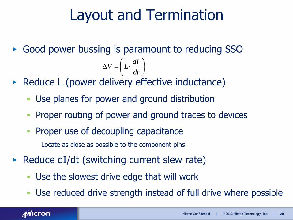
Layout and Termination
Good power bussing is paramount to reducing SSO
Reduce L (power delivery effective inductance)
Use planes for power and ground distribution
Proper routing of power and ground traces to devices
Proper use of decoupling capacitance
Locate as close as possible to the component pins
Reduce dI/dt (switching current slew rate)
Use the slowest drive edge that will work
Use reduced drive strength instead of full drive where possible
dt
dILV

21 Micron Confidential | ©2012 Micron Technology, Inc. |
Layout and Termination
RPDs induce board noise and are difficult to model
Splits/holes in reference planes
Connector discontinuities
Layer changes
Avoid RPDs if at all possible
Avoid crossing holes/splits in reference plane
Route signals so they reference the proper domain
Add power/ground vias to board
Especially in dense layer-change areas
Place decoupling capacitors near connectors
Solid return path
Split in return path

22 Micron Confidential | ©2012 Micron Technology, Inc. |
Layout and Termination
Intersymbol interference (ISI)
Occurs when data is random
Clocks do not have ISI
Multiple bits on the bus at the same time
Bus can’t settle from bit #1 before bit #2, etc.
Signal edges jitter due to previous bit’s energy still on
the bus
Ringing due to impedance mismatches
Low pass structures can cause ISI

23 Micron Confidential | ©2012 Micron Technology, Inc. |
Layout and Termination
Minimize ISI
Optimize layout
Keep board/DIMM impedances matched
Drive impedance should be same as Zo of transmission line
Terminate nets
Termination values should be the same as Zo of transmission
line
Select high-quality connector
Matched to board/DIMM impedance
Low mutual coupling

24 Micron Confidential | ©2012 Micron Technology, Inc. |
Layout and Termination
Crosstalk
Coupling on board, package, and connector from other
signals, including RPDs
Inductive coupling is typically stronger than capacitive coupling
When aggressors fire at same time as victim (e.g. data-to-
data coupling):
Victim edge speeds up or slows down, causing jitter
When aggressors do not fire at same time as victim (e.g.
data-to-command/address coupling):
Noise couples onto victim at time of aggressor switching

25 Micron Confidential | ©2012 Micron Technology, Inc. |
Layout and Termination
Minimize Crosstalk
Keep bits that switch on same “clock” edge routed together
Route data bits next to data bits; never next to CMD/ADDR bits
Isolate sensitive bits (strobes)
If need be, route next to signals that rarely switch
Separate traces by at least two to three preferred conductor
widths (more accurately, one would define by trace pitch and height
above reference plane)
Example: 5 mil trace located 5 mils from a reference plane
should have a 15 mil gap to its nearest neighbors to minimize
crosstalk
26 Micron Confidential | ©2012 Micron Technology, Inc. |
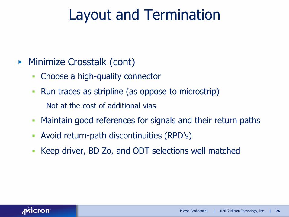
Layout and Termination
Minimize Crosstalk (cont)
Choose a high-quality connector
Run traces as stripline (as oppose to microstrip)
Not at the cost of additional vias
Maintain good references for signals and their return paths
Avoid return-path discontinuities (RPD’s)
Keep driver, BD Zo, and ODT selections well matched

27 Micron Confidential | ©2012 Micron Technology, Inc. |
Layout and Termination
Vref Noise
Induces strobe to data skews and reduces voltage margins
Power/ground plane noise
Crosstalk
Minimize Vref Noise
Use widest trace practical to route
From chip to decoupling capacitor
Use large spacing between Vref and neighboring traces
28 Micron Confidential | ©2012 Micron Technology, Inc. |
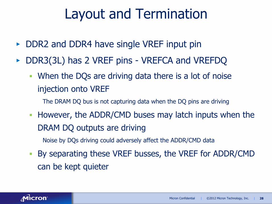
Layout and Termination
DDR2 and DDR4 have single VREF input pin
DDR3(3L) has 2 VREF pins - VREFCA and VREFDQ
When the DQs are driving data there is a lot of noise
injection onto VREF
The DRAM DQ bus is not capturing data when the DQ pins are driving
However, the ADDR/CMD buses may latch inputs when the
DRAM DQ outputs are driving
Noise by DQs driving could adversely affect the ADDR/CMD data
By separating these VREF busses, the VREF for ADDR/CMD
can be kept quieter

29 Micron Confidential | ©2012 Micron Technology, Inc. |
Layout and Termination
DDR3(3L): VREFCA and VREFDQ can have a common
source supply but should be separately routed and
decoupled at the DRAM
Place one decoupling capacitor per DRAM input
Use 0.1 uF and or 0.01 uF
Keep length from decoupling capacitor to the DRAM ball
short
Use a wide trace
Use the same reference plane as the related signals
For VREFDQ use the DQ buss reference plane
For VREFCA use the command and address bus reference plane

30 Micron Confidential | ©2012 Micron Technology, Inc. |
Layout and Termination
• Path length Mismatch
Path length differences between strobe and data bits
Also between clock and command/address/control
Any mismatch adds strobe-to-data skew
Check controller, most have adjustment tools to mitigate
mismatching
• Minimize Path length Mismatch
Balance the mismatch allowed
Large mismatches results in easier layout rules but reduce
timing margin in timing budgets
Minimal mismatches results in harder layout rules but have
minimal impact on timing budgets

31 Micron Confidential | ©2012 Micron Technology, Inc. |
Layout and Termination
Cin Mismatch
Differing input capacitances on receiver pins
Adds skew to input timings
RTT Mismatch
Termination resistors not at nominal value
Internal ODT on Data pins have smaller variation than on
DDR2
They are calibrated (so is DRAM’s Ron)
External termination resistor variation must be accounted for
Consider one-percent resistors

32 Micron Confidential | ©2012 Micron Technology, Inc. |
Layout and Termination
High-speed signals must maintain a solid reference plane
Reference plane may be either VDD or ground
For DDR3 UDIMM systems, the DQ busses are referenced to
ground while the ADDR/CMD and clock are referenced to VDD
All signals may be referenced to ground if the layout allows
Best signaling is obtained when a constant reference plane
is maintained
If this is not possible try to make the transitions near
decoupling capacitors
Signal Power Plane
Ground Plane
Cap

33 Micron Confidential | ©2012 Micron Technology, Inc. |
QUESTIONS?
June 6, 2013


35 Micron Confidential | ©2012 Micron Technology, Inc. |
Develop Timing Budgets
Example of a DDR3 Write Timing budget for 2 slots

36 Micron Confidential | ©2012 Micron Technology, Inc. |
PtP Termination

37 Micron Confidential | ©2012 Micron Technology, Inc. |
PtP Termination
The best signaling is achieved when the driver impedance
matches the trace impedance
Termination impedance matched as well
For memory down applications 50 to 60 may be
adequate but an ideal system would use a 40 impedance
DRAM has optional 40 or 48 driver (Ronbase is 18 or 34)
Larger ODT values are for generally used during Writes
Smaller ODT values are for generally used during standby
If single rank then ODT during standby is not needed

38 Micron Confidential | ©2012 Micron Technology, Inc. |
Source vs. Source and load termination
Source - Driver’s impedance is termination
Lower power
Larger voltage margin
Overshoot / fast slew rates can be a problem in some case
Series R can improve results and save power over ODT
Source & load - Driver’s impedance and ODT/VTT termination
Less sensitive to changes in the value of Ron
Less prone to overshooting the supply rails
Slower slew rates

39 Micron Confidential | ©2012 Micron Technology, Inc. |
Terminating PtP DQ Bus
Generally use higher impedance DQ driver option
Usually slightly less than Zo
DDR4 requires use of ODT termination due to POD
DDR2 and DDR3(3L) do not mandate ODT usage, but
should be used if possible in most cases
Series resistor likely should be added if ODT is not used
Line length < 2”, one series resistor in middle seems acceptable
Line length > 2”, one series resistor on each end might work
If ODT power is too much, disable ODT and use series resistor
Reduces I/O switching current by approx. 40%
Will slow down edge rate a little bit too

40 Micron Confidential | ©2012 Micron Technology, Inc. |
Terminating PtP DQ Bus
Source termination
DDR2 has Ron value of 18Ω; Reduced Ron value of approx 40Ω
DDR3(3L) has Ron value of 34Ω; Reduced Ron value of 40Ω
DDR4 has Ron value of 34Ω; Reduced Ron value of 48Ω
ODT load termination
DDR2 has ODT values of 50Ω, 75Ω and 150Ω
DDR3(3L) has ODT values of 20Ω, 30Ω , 40Ω , 60Ω, and 120Ω
DDR4 has ODT values of 34Ω, 40Ω , 48Ω , 60Ω, 80Ω, 120Ω, and 240Ω
Larger ODT provides voltage margin and uses less power
too large ODT then overshoot occurs and jitter increases
June 6, 2013

41 Micron Confidential | ©2012 Micron Technology, Inc. |
Terminating Pt2/4P Command/Address Bus
The CMD/ADDR bus is more sensitive than the DQ bus to
input slew rate
Faster slew rates introduce higher frequency harmonics onto the
bus, degrading signal integrity
Faster is not always better when it comes to slew rate
Controller Ron, lead length, and board impedance
determine termination requirements
Series resistor probably ok at lower frequencies
Series resistor with parallel termination to Vtt should be used at
higher frequencies
Larger R = more voltage margin but more jitter; find best trade off via
simulations
June 6, 2013

42 Micron Confidential | ©2012 Micron Technology, Inc. |
Command/Address Topologies
Tree
Excellent performance - Until you run out of bandwidth
Hardest to route
Hybrid tree
Good performance
Easier to route than tree
Daisy chain
Good performance
Easiest to route
Best bandwidth – works at highest rates and largest loading

43 Micron Confidential | ©2012 Micron Technology, Inc. |
Pt4P CMD/ADDR Bus Termination
Tree Daisy-chain “fly-by” Hybrid tree
-Route +Skew
Bandwidth +Performance
Route Skew
Bandwidth Performance
+Route -Skew
+Bandwidth +Performance

44 Micron Confidential | ©2012 Micron Technology, Inc. |
Multiple Rank Termination

45 Micron Confidential | ©2012 Micron Technology, Inc. |
Multiple Rank Termination
Design guides on web – WWW.Micron.com
Systems are complex and require simulation
DDR2 modules use Tree topology
DDR3(3L) modules use Daisy Chain or “fly-by” topology
DDR4 modules use Daisy Chain or “fly-by” topology
Daisy Chain reduces number of stubs and stub length
Address/Command/Control VTT termination at end of bus
More Address/Command/Control bandwidth
Has interconnect skew between clock and strobe at every
DRAM on DIMM must be de-skewed

46 Micron Confidential | ©2012 Micron Technology, Inc. |
Backup - Termination
DDR3 PtP Examples
June 6, 2013

47 Micron Confidential | ©2012 Micron Technology, Inc. |
PtP Layout and Termination Analysis
The DQ bus is a single connection from the memory
controller to a single DRAM
DDR3 with Data rate = 1,333MT/s
Zo for bus transmission lines is 50Ω
What is the best way to terminate the DQ bus?
Consider three choices
Source termination
Source and load termination - on die termination (ODT)
Source and series termination

48 Micron Confidential | ©2012 Micron Technology, Inc. |
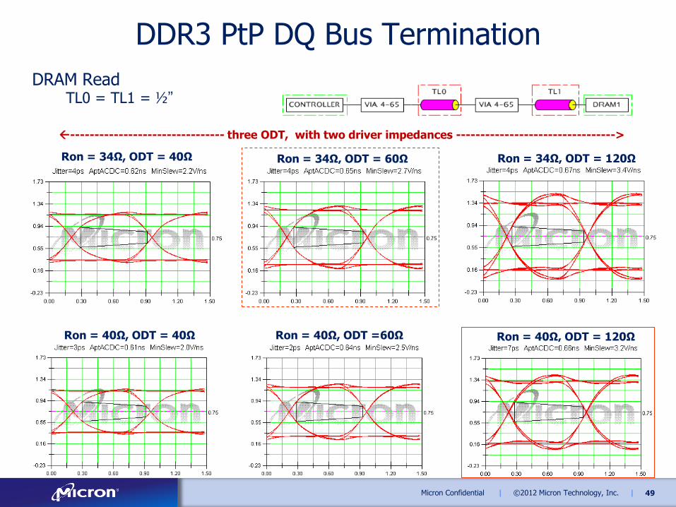
DDR3 PtP DQ Bus Termination
DRAM Read TL0 = TL1 = ½”
Ron = 34Ω, ODT = 0Ω
So
urc
e
So
urc
e a
nd
Lo
ad
Ron = 40Ω, ODT = 0Ω Ron = 48Ω, ODT = 0Ω
Ron = 34Ω, ODT = 60Ω Ron = 40Ω, ODT = 60Ω Ron = 48Ω, ODT = 60Ω
------------------------------------ ODT off, vary driver impedance ------------------------------------->
49 Micron Confidential | ©2012 Micron Technology, Inc. |
DDR3 PtP DQ Bus Termination
DRAM Read TL0 = TL1 = ½”
Ron = 40Ω, ODT = 40Ω Ron = 40Ω, ODT =60Ω Ron = 40Ω, ODT = 120Ω
Ron = 34Ω, ODT = 40Ω Ron = 34Ω, ODT = 60Ω Ron = 34Ω, ODT = 120Ω
-------------------------------- three ODT, with two driver impedances --------------------------------->

50 Micron Confidential | ©2012 Micron Technology, Inc. |
DDR3 PtP DQ Bus Termination
DRAM Read MB1 = MB2 = B2 = ½”
Use DDR1, adjust settings and turn VTT off
Rs = 20Ω, Ron = 40Ω, ODT = off Rs = 20Ω, Ron = 34Ω, ODT = off
Rs = 0Ω, Ron = 40Ω, ODT = off Rs = 10Ω, Ron = 40Ω, ODT = off
----------------------------- Various Series R, with two driver impedances ------------------------------>

51 Micron Confidential | ©2012 Micron Technology, Inc. |
DDR3 PtP DQ Bus Termination
Source/series vs. Source/load termination
Source/series mitigates the overshoot and slew rate issues
with source yet offers power savings
Source and load (ODT) still provides the largest data eye
Ron = 40Ω, ODT = off, Rs = 10Ω, Ron = 40Ω, ODT = 120Ω
52 Micron Confidential | ©2012 Micron Technology, Inc. |
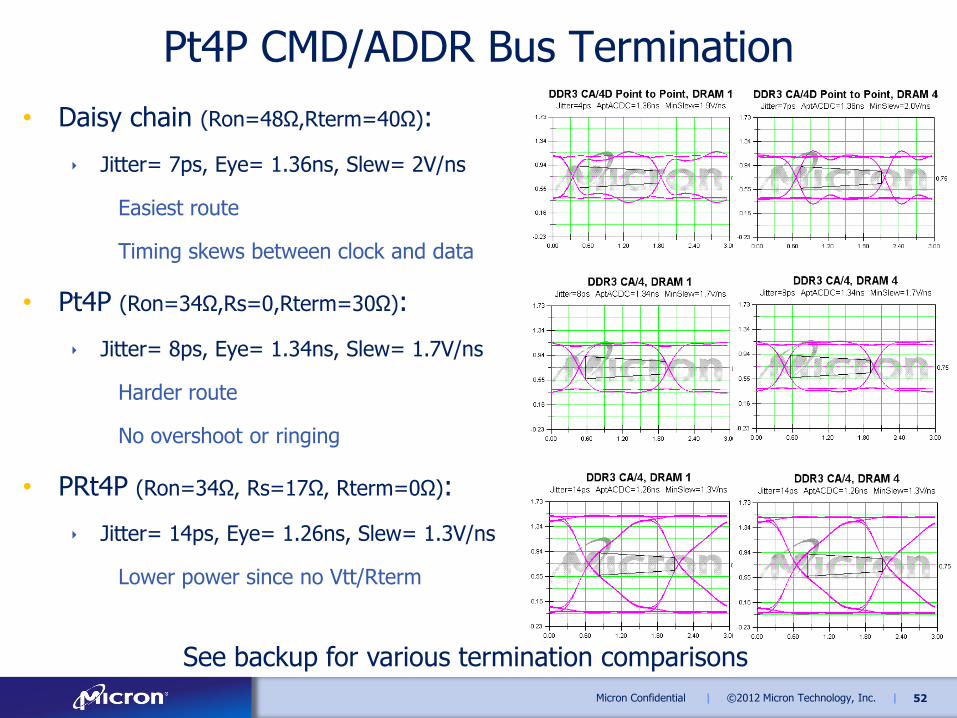
Pt4P CMD/ADDR Bus Termination
• Daisy chain (Ron=48Ω,Rterm=40Ω):
‣ Jitter= 7ps, Eye= 1.36ns, Slew= 2V/ns
Easiest route
Timing skews between clock and data
• Pt4P (Ron=34Ω,Rs=0,Rterm=30Ω):
‣ Jitter= 8ps, Eye= 1.34ns, Slew= 1.7V/ns
Harder route
No overshoot or ringing
• PRt4P (Ron=34Ω, Rs=17Ω, Rterm=0Ω):
‣ Jitter= 14ps, Eye= 1.26ns, Slew= 1.3V/ns
Lower power since no Vtt/Rterm
See backup for various termination comparisons

53 Micron Confidential | ©2012 Micron Technology, Inc. |
Backup – DDR4
Comparison to DDR2 and DDR3(3L)
June 6, 2013

54 Micron Confidential | ©2012 Micron Technology, Inc. |
DDR2 to DDR3(3L) to DDR4 Comparison
6/6/2013 54
Features/Options DDR2 DDR3(3L) DDR4
Voltage (core, /IO) 1.8V 1.5V 1.2V
Low Voltage Std. No DDR3L at 1.35V Probably 1.05V
Vref Inputs 1 – DQs/CMD/ADDR 2 – DQs and CMD/ADDR 1 –CMD/ADDR
Densities Defined 256Mb–4Gb 512Mb–8Gb 2Gb–16Gb
Internal Banks 4 8 8 16
Bank Groups (BG) 0 0 4
Page Size – x4/x8/16 1KB/1KB/2KB 1KB/1KB/2KB 512B/1KB/2KB
tCK – DLL enabled 125MHz to 400MHz 300MHz to 1066MHz 625MHz to 1.6GHz
tCK – DLL disabled Optional, ≤125MHz Optional, ≤125MHz Feature, ≤125MHz
Data Rate - Mb/s 400/533/667/800
plus1066
800 /1066/1333/1600
plus1866, 2133
1600/1866/2133
/2400/ 2667/3200
Prefetch 4-bits (2 clocks) 8-bits (4 clocks) 8-bits (4 clocks)
Burst length BL4, BL8 BC4, BL8 BC4, BL8
Burst type (1) Fixed (1) Fixed, (2) OTF (1) Fixed, (2) OTF

55 Micron Confidential | ©2012 Micron Technology, Inc. |
DDR2 to DDR3(3L) to DDR4 Comparison
6/6/2013 55
Features/Options DDR2 DDR3(3L) DDR4
Access (CL,tRCD,tRP) 14ns+/- 14ns+/- 14ns+/-
Additive Latency 0, 1,2,3,4 0, CL-1, CL-2 0, CL-1, CL-2
READ Latency (RL) AL + CL AL + CL AL + CL
WRITE Latency RL-1 AL + CWL AL + CWL
Data Strobes Single or Differential Differential Only Differential Only
Driver / ODT Calibration none 240Ω Ext. Resistor 240Ω Ext Resistor
DQ Driver (STD) 18Ω (13Ω to 24Ω) 34Ω (31Ω to 38Ω) 34Ω (31Ω to 38Ω)
DQ Driver (ALT) 40Ω (21Ω to 61Ω) 40Ω (36Ω to 44Ω) 40Ω (36Ω to 44Ω)
DQ Bus Termination ODT ODT ODT
DQ Bus SSTL18 SSTL15 POD12
Rtt Values 150, 75, 50Ω 120, 60, 40, 30, 20Ω 240, 120, 80, 60, 48,
40, 34Ω
Rtt disabled at READs No No Yes
ODT Modes Nominal, Dynamic Nominal, Dynamic Nominal, Dynamic, Park

56 Micron Confidential | ©2012 Micron Technology, Inc. |
DDR2 to DDR3(3L) to DDR4 Comparison
6/6/2013 56
Features/Options DDR2 DDR3(3L) DDR4
ODT Input Control Required Driven Required Driven Not Required Driven
MultiPurpose Register None 1 Defined, 3 RFU 3 Defined, 1 RFU
Write Leveling None DQS captures CK DQS captures CK
RESET# None Dedicated input Dedicated input
VPP Supply none none 2.5V
VREFDQ Calibration none none Supported/Required
Bank Group none none four
Low-power Auto SR None None (ASR opt.) supported
Temperature Controlled
Refresh (TCR) none none supported
Fine Granularity Refresh none none supported
CMD/ADDR Latency none none supported
Data Bus Write CRC none none supported
Data Bus Inversion (DBI) none none supported

57 Micron Confidential | ©2012 Micron Technology, Inc. |
DDR2 to DDR3(3L) to DDR4 Comparison
6/6/2013 57
Features/Options DDR2 DDR3(3L) DDR4
Per DRAM Addressability none none supported
C/A Parity none none supported
Gear-Down Mode none none supported
Connectivity Test Mode none none supported
Max. Power Savings none none supported
Program READ Preamble none none supported
Program WRITE Preamble none none supported
READ Preamble Training none none supported
Self Refresh Abort none none supported
Command Input (ACT_n) none none supported
Pin-out/Package (FBGA) 60-ball; x4, x8
84-ball; x16
78-ball; x4, x8
96-ball; x16
78-ball; x4, x8
96-ball; x16
UDIMM, RDIMM 240pin 240pin 288pin
SODIMM 200pin 204pin 256pin

58 Micron Confidential | ©2012 Micron Technology, Inc. |
Backup – DDR4 Features
Select New Features
June 6, 2013

59 Micron Confidential | ©2012 Micron Technology, Inc. |
DQ Output Driver
6/6/2013 59
DDR2, 3(3L) – Push-Pull DDR4 – Pseudo Open Drain

60 Micron Confidential | ©2012 Micron Technology, Inc. |
DDR4 vs DDR3(3L)/2 Bank Architecture
June 6, 2013
DDRx MT/s (min) MT/s (max) tCK (max) tCK (min) Preftech Internal
Access (min)
2 400 800 5ns 2.5ns 4n 5ns
3 800 1600 2.5ns 1.25ns 8n 5ns
4 1600 3200 1.25ns 0.625ns 16n 5ns
4 1600 3200 1.25ns 0.625ns 8n 2.5ns
DDR3 DDR4 DDR4 adder if like DDR3
tCCD_s tCCD_L
tCCD_S @ 4CK = 2.5ns tCCD_L @ 5CK = 5.3ns

61 Micron Confidential | ©2012 Micron Technology, Inc. |
MPR Operation
Multi-Purpose Register is a useful tool that can be used for
various ways
Training
DRAM controller receiver training
DRAM controller DQS to DQ phase training
Clock to address phase training
Debug
MPR provides a known response when rest is uncertain
RAS Support
Logging of C/A parity and CRC error information
Mode Register Confirmation
June 6, 2013

62 Micron Confidential | ©2012 Micron Technology, Inc. |
MPR Registers
June 6, 2013
Logical Page MR3[1:0]
Description MPR Location
[BA1:BA0]
MPR Bit Write Location [7:0]
7 6 5 4 3 2 1 0
Read Burst Order (serial mode)
UI0 UI1 UI2 UI3 UI4 UI5 UI6 UI7
00 = Page 0 Training Patterns
00 = MPR0 0 1 0 1 0 1 0 1
01 = MPR1 0 0 1 1 0 0 1 1
10 = MPR2 0 0 0 0 1 1 1 1
11 = MPR3 0 0 0 0 0 0 0 0
01 = Page 1 C/A Parity Error Log
00 = MPR0 A[7] A[6] A[5] A[4] A[3] A[2] A[1] A[0]
01 = MPR1 A[15]/ CAS_n
A[14]/ WE_n
A[13] A[12] A[11] A[10] A[9] A[8]
10 = MPR2 PAR ACT_n BG[1] BG[0] BA[1] BA[0] A[17] A[16]/ RAS_n
11 = MPR3 CRC Error
Status
C/A Parity Error Status
C/A Parity Latency C[2] C[1] C[0]
10 = Page 2 MRS
Readout
00 = MPR0 PPR RFU Rtt_WR Setting
Temp Sensor Status
CRC Write Enable
Rtt_WR Setting
01 = MPR1 VrefDQ Training Range
VrefDQ Training Value Gear-down Enable
10 = MPR2 CAS Latency RFU CAS Write Latency
11 = MPR3 Rtt_Nom Setting Rtt_Park Setting Driver Impedance
11 = Page 3 RFU
00 = MPR0 RFU RFU RFU RFU RFU RFU RFU RFU
01 = MPR1 RFU RFU RFU RFU RFU RFU RFU RFU
10 = MPR2 RFU RFU RFU RFU RFU RFU RFU RFU
11 = MPR3 RFU RFU RFU RFU RFU RFU RFU RFU

63 Micron Confidential | ©2012 Micron Technology, Inc. |
DDR4 Write CRC Error

64 Micron Confidential | ©2012 Micron Technology, Inc. |
DDR4 Writes - CRC Flow

65 Micron Confidential | ©2012 Micron Technology, Inc. |
C/A Parity
C/A Parity provides parity checking of command and
address buses

66 Micron Confidential | ©2012 Micron Technology, Inc. |
C/A Parity Flow

67 Micron Confidential | ©2012 Micron Technology, Inc. |
DDR3L vs DDR4 Power (with VPP)
June 6, 2013
DDR3L vs DDR4 IDD
specs
Both 30nm 4Gb x8
1866
DDR4 power includes
both IDD and IPP current

68 Micron Confidential | ©2012 Micron Technology, Inc. |
Backup - Clock Jitter
Highlight of JEDEC definitions
June 6, 2013

69
tCKavg is calculated as the average clock period across any consecutive 200 clock
cycle window
Sometimes referred to as the “ideal” or “nominal” clock
Clock variations should fit within a random Gaussian Distribution
Does not include SSC effects
tCKavg
Clock Jitter: tCKavg
tCK distribution due to jitter
t(ns)

70
Clock Jitter: tJITper
• tJITper is Clock Period Jitter; and is the deviation of any single clock period from tCKavg
• tJITper(min/max) is the largest deviation of any single clock period from tCKavg
This is an absolute limit, not an RMS or Sigma value Micron Design Line article provides guidance on dealing with RMS clock jitter values,
or jitter values that exceed the absolute clock period limit - TN-04-56
tJITpermin tJITpermax
Minimum tCK
Allowed
tCK distribution due to jitter
tCKavg
Maximum tCK
Allowed

71
tERR(nper) is defined as the cumulative error
across consecutive n cycles relative to n
tCKavgs
A period of tCKavg * n (number of clocks)
can not be deviated from by more than
tERR(nper) (+ or -)
Negative is primary concern for a DRAM
Clock periods greater than tCKavg (slower) will
offset clock periods less than tCKavg (faster)
when determining cumulative error
tCKavg
tJITcc
tJITpermin tJITpermax
tCKx
tCKx+1
tCKx+2
tCKx+3
- +
tCKmin tCKavg
Clock Jitter: tERRnper
Distribution of Clocks

72
Clock Jitter: tERRnper tERR(nper) is defined for different sets of cumulative jitter error parameters
n is for 2, 3, 4, 5, 6-10, 11-50 clocks for DDR2
n is for 2, 3, 4, 5, 6, 7, 8, 9, 10, 11, 12; 13-50 clocks = (1+0.68Ln[n]) * tJITpermin for DDR3/4
Since jitter is a Gaussian distribution, the cumulative error, either positive or negative, is not
a summation of the absolute values (n-clocks times tJITpermin or tJITpermax)
0
100
200
300
400
500
600
700
800
900
1000
0 1 2 3 4 5 6 7 8 9 10 11 12
667 tERR(xper)
ps
WC Theoretical Error
667 Spec
2*tJITper
3*tJITper
4*tJITper
5*tJITper
6*tJITper
7*tJITper
8*tJITper
1*tJITper

73
Modulation frequency of 20 to 60KHz allowed, with up to 1% tCKavg deviation
If the DLL is locked prior to SSC being enabled, then tCKavg deviation can
be up to 2% tCKavg
SSC (Spread Spectrum Clocking)
Top Related