


Languages
Pages
Legal

AZ DISPLAYSSPECIFICATIONS FOR
LIQUID CRYSTAL DISPLAY
CUSTOMER APPROVAL
※ PART NO. : ATM0700L6B-T (AZ DISPLAYS) VER1.4
APPROVAL COMPANYCHOP
CUSTOMERCOMMENTS
AZ DISPLAYS ENGINEERING APPROVAL
DESIGNED BY CHECKED BY APPROVED BY
HERBERT

ATM0700L6B-T(AZ DISPLAYS) TFT MODULE VER1.4
AZ DISPLAYS 1
REVISION RECORDREVISION REVISION DATE PAGE CONTENTS
VER1.0
VER1.1
VER1.2
VER1.3
VER1.4
2012-01-31
2013-01-10
2013-07-25
2014-02-08
2014-11-18
16
ALL
11
18
FIRST ISSUED
MODIFY MECHANICAL DIAGRAM
CHANGE SPEC FORMAT
CHANGE 4.2.3 TIMING DEFINE
REMOVE SCREW HOLE ON LEFT SIDE OF LCM

ATM0700L6B-T(AZ DISPLAYS) TFT MODULE VER1.4
AZ DISPLAYS 2
※ CONTENTS
1.0 GENERAL SPECIFICATION
2.0 BLOCK DIAGRAM
3.0 PIN ASSIGNMENT
4.0 OPERATING SPECIFICATIONS
5.0 OPTICAL CHARACTERISTICS
6.0 RELIABILITY TEST
7.0 PRECAUTION FOR USING LCM
8.0 MECHANICAL DIAGRAM
9.0 PACKAGE DRAWING
10.0 INSPECTION SPECIFICATION
ATM0700L6B-T(AZ DISPLAYS) TFT MODULE VER1.4
AZ DISPLAYS 3
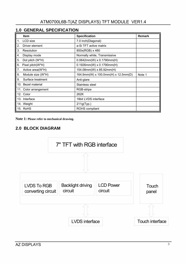
1.0 GENERAL SPECIFICATIONItem Specification Remark
1. LCD size 7.0 inch(Diagonal)2. Driver element a-Si TFT active matrix3. Resolution 800x(RGB) x 4804. Display mode Normally white, Transmissive5. Dot pitch (W*H) 0.0642mm(W) x 0.1790mm(H)6. Pixel pitch(W*H) 0.1926mm(W) x 0.1790mm(H)7. Active area(W*H) 154.08mm(W) x 85.92mm(H)8. Module size (W*H) 164.9mm(W) x 100.0mm(H) x 12.5mm(D) Note 19. Surface treatment Anti-glare10. Bezel material Stainless steel11. Color arrangement RGB-stripe12. Color 262K13. Interface 18bit LVDS interface14. Weight 211g(Typ.)15. RoHS ROHS compliant
Note 1: Please refer to mechanical drawing.
2.0 BLOCK DIAGRAM
Touch interface
Touchpanel
LVDS interface
LVDS To RGB converting circuit
LCD Power circuit
Backlight driving circuit
7'' TFT with RGB interface

ATM0700L6B-T(AZ DISPLAYS) TFT MODULE VER1.4
AZ DISPLAYS 4
3.0 PIN ASSIGNMENTConnector on LCM : HIROSE DF19G-20P-1H or compatible,mating with HIROSE DF19-20S-1C orcompatible
Pin No. Symbol Function
1 TX0- Negative LVDS differential data input(R0-R5,G0)*3
2 TX0+ Positive LVDS differential data input(R0-R5,G0)*3
3 VSS*1 Ground
4 TX1- Negative LVDS differential data input(G1-G5,B0-B1)*3
5 TX1+ Positive LVDS differential data input(G1-G5,B0-B1)*3
6 VSS*1 Ground
7 TX2- Negative LVDS differential data input(B2-R5,HS,VS,DE)*3
8 TX2+ Positive LVDS differential data input(B2-R5,HS,VS,DE)*3
9 VSS*1 Ground
10 CLK- Clock Signal(-)
11 CLK+ Clock signal(+)
12 VSS*1 Ground
13 NC*2 Non Connection(open)
14 NC*2 Non Connection(open)
15 VDD +3.3V power supply for logic and LCM power
16 VDD +3.3V power supply for logic and LCM power
17 BL+ +5.0V Backlight driving circuit power supply
18 BL- Backlight driving circuit ground
19 PWM Backlight ON/OFF/Dimming control(PWM:100~1000HZ, 0~100%)
20 VSS*1 Ground
Note 1) Please connect VSS pin to ground. Don’t use it as no-connect nor connection with high impedance.
Note 2) Please connect NC pin to nothing. Don’t connect it to ground nor to other signal input.
Note 3) Refer to next page.

ATM0700L6B-T(AZ DISPLAYS) TFT MODULE VER1.4
AZ DISPLAYS 5
RECOMMENDED TRANSMITTER(DS90C365) TO LCM INTERFACE ASSIGNMENT

ATM0700L6B-T(AZ DISPLAYS) TFT MODULE VER1.4
AZ DISPLAYS 6
Tout Panel SectionFPC Connector is used for the module electronics interface. The recommended model isFH12-4S-1SH manufactured by Hirose.
Pin No. Symbol I/O Function Remark
4 Y1 Top Top electrode – differential analog
3 X1 Left Left electrode – differential analog
2 Y2 Bottom Bottom electrode – differential analog
1 X2 Right Right electrode – differential analog
TP LAYOUT
4 1
Y1
X2X1
Y2

ATM0700L6B-T(AZ DISPLAYS) TFT MODULE VER1.4
AZ DISPLAYS 7
4.0 Operating Specification4.1 ABSOLUTE MAXIMUM RATINGS
Item Symbol Min Typ Max Unit
Operating temperature Top -20 - 70 ºC
Storage temperature Tst -30 - 80 ºC
Input voltage Vin Vss-0.3 - Vdd+0.3 V
Supply voltage for logic Vdd- Vss -0.3 - 3.6 V
4.1.1 Typical Operation ConditionsItem Symbol Condition Min Typ Max Unit
Power Supply Voltage VDD Ta=25ºC 3.0 3.3 3.6 V
Power Supply current IDD VDD=3.3V - 140 - mA
BL circuit voltage VLED(PIN17) Ta=25ºC 4.8 5.0 5.2 V
BL circuit current ILED VLED=5V - 468 - mA
Input voltage (high) Vih H level 2.0 - Vdd V
Input voltage (low) Vil L level Vss - 0.8 V
4.1.2 Backlight driving conditions
Item Symbol Condition Min Typ Max Unit Remark
Backlight Voltage(To LED directly)
VBL IBL=200mA 9.3 9.9 10.5 V Note1
LED life time -- -- 30000 -- -- H Note2,3
Note 1: The LED Supply Voltage is defined by the number of LED at Ta=25℃ and IBL =200mA.Note 2: The “LED life time” is defined as the module brightness decrease to 50% original brightness atTa=25℃ and IBL =200mA.Note 3: Please make sure the LCM works under well heat dissipated condition, and to prolong the lifetime, pleasereduce the driving current when environment temperature increases,.
ATM0700L6B-T(AZ DISPLAYS) TFT MODULE VER1.4
AZ DISPLAYS 8
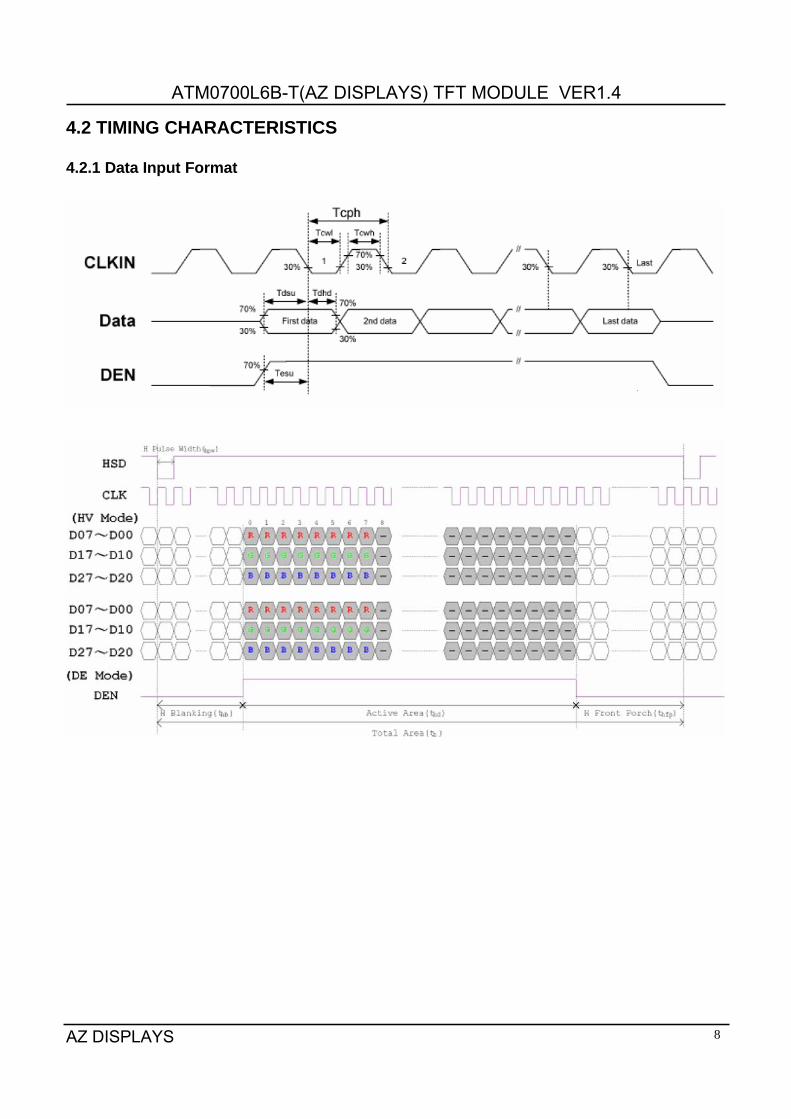
4.2 TIMING CHARACTERISTICS
4.2.1 Data Input Format
ATM0700L6B-T(AZ DISPLAYS) TFT MODULE VER1.4
AZ DISPLAYS 9
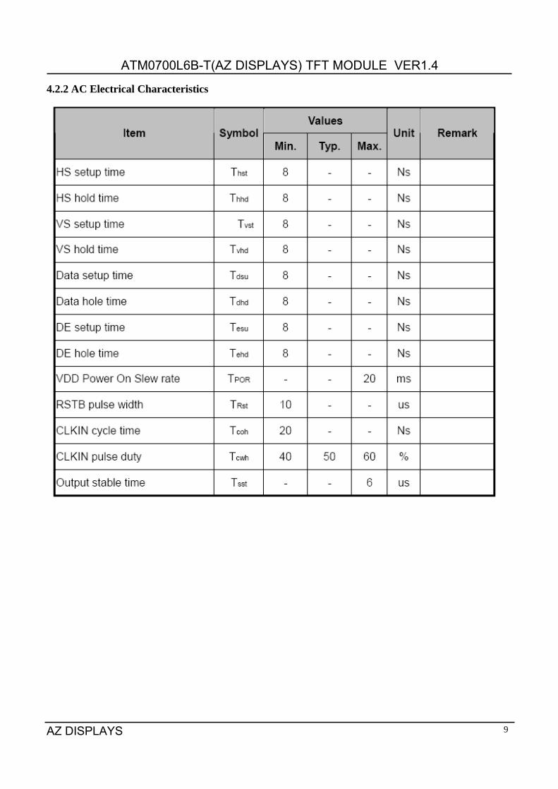
4.2.2 AC Electrical Characteristics
ATM0700L6B-T(AZ DISPLAYS) TFT MODULE VER1.4
AZ DISPLAYS 10
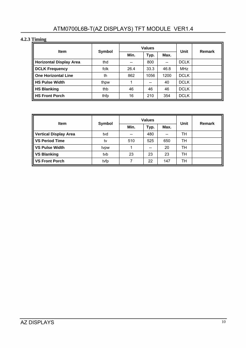
4.2.3 Timing
Item SymbolValues
Unit RemarkMin. Typ. Max.
Horizontal Display Area thd -- 800 -- DCLK
DCLK Frequency fclk 26.4 33.3 46.8 MHz
One Horizontal Line th 862 1056 1200 DCLK
HS Pulse Width thpw 1 -- 40 DCLK
HS Blanking thb 46 46 46 DCLK
HS Front Porch thfp 16 210 354 DCLK
Item SymbolValues
Unit RemarkMin. Typ. Max.
Vertical Display Area tvd -- 480 -- TH
VS Period Time tv 510 525 650 TH
VS Pulse Width tvpw 1 -- 20 TH
VS Blanking tvb 23 23 23 TH
VS Front Porch tvfp 7 22 147 TH
ATM0700L6B-T(AZ DISPLAYS) TFT MODULE VER1.4
AZ DISPLAYS 11
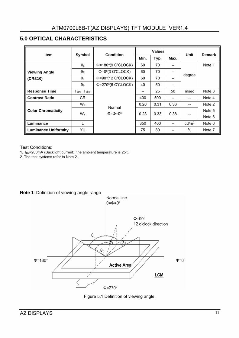
5.0 OPTICAL CHARACTERISTICS
Item Symbol ConditionValues
Unit RemarkMin. Typ. Max.
Viewing Angle(CR≥10)
θL Φ=180o(9 O'CLOCK) 60 70 --
degree
Note 1
θR Φ=0o(3 O'CLOCK) 60 70 --
θT Φ=90o(12 O'CLOCK) 60 70 --
θB Φ=270o(6 O'CLOCK) 40 50 --
Response Time TON + TOFF
NormalΘ=Φ=0o
-- 25 50 msec Note 3
Contrast Ratio CR 400 500 -- -- Note 4
Color ChromaticityWX 0.26 0.31 0.36 -- Note 2
Note 5Note 6
WY 0.28 0.33 0.38 --
Luminance L 350 400 -- cd/m2 Note 6
Luminance Uniformity YU 75 80 -- % Note 7
Test Conditions:1. IBL=200mA (Backlight current), the ambient temperature is 25℃.2. The test systems refer to Note 2.
Note 1: Definition of viewing angle range
Figure 5.1 Definition of viewing angle.

ATM0700L6B-T(AZ DISPLAYS) TFT MODULE VER1.4
AZ DISPLAYS 12
Note 2: Definition of optical measurement system.The optical characteristics should be measured in dark room. After 30 minutes operation, the optical properties aremeasured at the center point of the LCD screen. (Response time is measured by Photo detector TOPCON
Figure 5.2 Optical measurement system setup
Note 3: Definition of Response timeThe response time is defined as the LCD optical switching time interval between “White” state and “Black” state. Risetime (TON) is the time between photo detector output intensity changed from 90% to 10%. And fall time (TOFF) is thetime between photo detector output intensity changed from 10% to 90%.
Figure 5.3 Definition of response.
Note 4: Definition of contrast ratio
ATM0700L6B-T(AZ DISPLAYS) TFT MODULE VER1.4
AZ DISPLAYS 13
Note 5: Definition of color chromaticity (CIE1931)Color coordinates measured at center point of LCD.
Note 6: All input terminals LCD panel must be ground while measuring the center area of the panel.
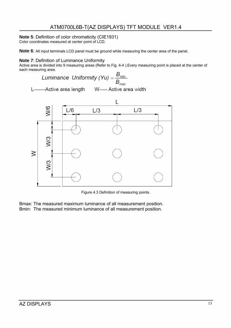
Note 7: Definition of Luminance UniformityActive area is divided into 9 measuring areas (Refer to Fig. 4-4 ).Every measuring point is placed at the center ofeach measuring area.
Figure 4.3 Definition of measuring points.
Bmax: The measured maximum luminance of all measurement position.Bmin: The measured minimum luminance of all measurement position.
ATM0700L6B-T(AZ DISPLAYS) TFT MODULE VER1.4
AZ DISPLAYS 14
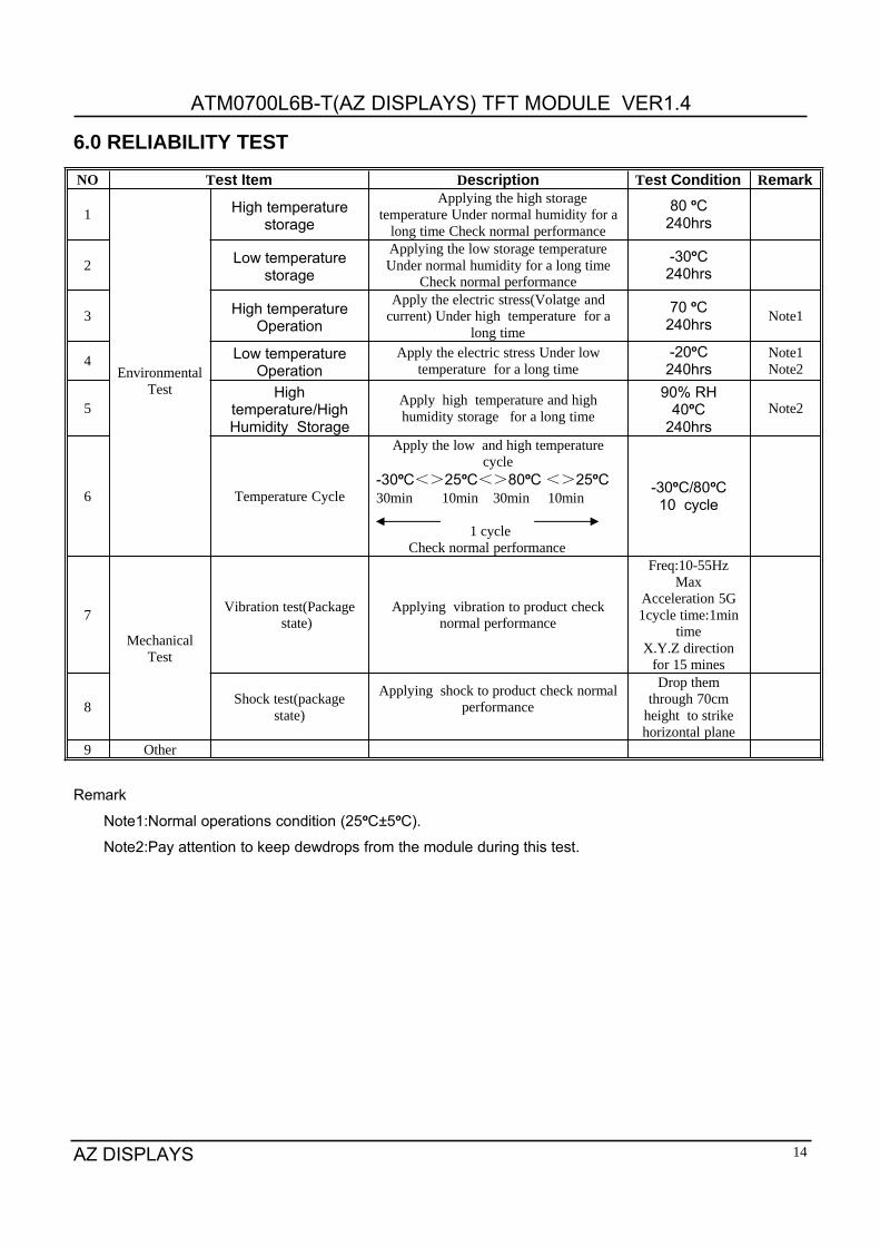
6.0 RELIABILITY TEST
NO Test Item Description Test Condition Remark
1
EnvironmentalTest
High temperaturestorage
Applying the high storagetemperature Under normal humidity for a
long time Check normal performance
80 ºC240hrs
2 Low temperaturestorage
Applying the low storage temperatureUnder normal humidity for a long time
Check normal performance
-30ºC240hrs
3 High temperatureOperation
Apply the electric stress(Volatge andcurrent) Under high temperature for a
long time
70 ºC240hrs Note1
4 Low temperatureOperation
Apply the electric stress Under lowtemperature for a long time
-20ºC240hrs
Note1Note2
5High
temperature/HighHumidity Storage
Apply high temperature and highhumidity storage for a long time
90% RH40ºC
240hrsNote2
6 Temperature Cycle
Apply the low and high temperaturecycle
-30ºC<>25ºC<>80ºC <>25ºC30min 10min 30min 10min
1 cycleCheck normal performance
-30ºC/80ºC10 cycle
7
MechanicalTest
Vibration test(Packagestate)
Applying vibration to product checknormal performance
Freq:10-55HzMax
Acceleration 5G1cycle time:1min
timeX.Y.Z direction
for 15 mines
8 Shock test(packagestate)
Applying shock to product check normalperformance
Drop themthrough 70cm
height to strikehorizontal plane
9 Other
Remark
Note1:Normal operations condition (25ºC±5ºC).
Note2:Pay attention to keep dewdrops from the module during this test.
ATM0700L6B-T(AZ DISPLAYS) TFT MODULE VER1.4
AZ DISPLAYS 15
7.0 PRECAUTION FOR USING LCM1. When design the product with this LCD Module, make sure the viewing angle matches to its purpose of usage.
2. As LCD panel is made of glass substrate, Dropping the LCD module or banging it against hard objects may
cause cracking or fragmentation. Especially at corners and edges.
3. Although the polarizer of this LCD Module has the anti-glare coating, always be careful not to scratch its
surface. Use of a plastic cover is recommended to protect the surface of polarizer.
4. If the LCD module is stored at below specified temperature, the LC material may freeze and be deteriorated. If
it is stored at above specified temperature, the molecular orientation of the LC material may change to Liquid
state and it may not revert to its original state. Excessive temperature and humidity could cause polarizer peel
off or bubble. Therefore, the LCD module should always be stored within specified temperature range.
5. Saliva or water droplets must be wiped off immediately as those may leave stains or cause color changes if
remained for a long time. Water vapor will cause corrosion of ITO electrodes.
6. If the surface of LCD panel needs to be cleaned, wipe it swiftly with cotton or other soft cloth. If it is not still
clean enough, blow a breath on the surface and wipe again.
7. The module should be driven according to the specified ratings to avoid malfunction and permanent damage.
Applying DC voltage cause a rapid deterioration of LC material. Make sure to apply alternating waveform by
continuous application of the M signal. Especially the power ON/OFF sequence should be kept to avoid latchup
of driver LSIs and DC charge up to LCD panel.
8. Mechanical Considerations
a) LCM are assembled and adjusted with a high degree of precision. Avoid excessive shocks and do not
make any alterations or modifications. The following should be noted.
b) Do not tamper in any way with the tabs on the metal frame.
c) Do not modify the PCB by drilling extra holes, changing its outline, moving its components or modifying its
pattern.
d) Do not touch the elastomer connector; especially insert a backlight panel (for example, EL).
e) When mounting a LCM makes sure that the PCB is not under any stress such as bending or twisting.
Elastomer contacts are very delicate and missing pixels could result from slight dislocation of any of the
elements.
f) Avoid pressing on the metal bezel, otherwise the elastomer connector could be deformed and lose
contact, resulting in missing pixels.
9. Static Electricity
a) Operator
Ware the electrostatics shielded clothes because human body may be statically charged if not ware shielded clothes.
Never touch any of the conductive parts such as the LSI pads; the copper leads on the PCB and the interface
terminals
with any parts of the human body.
b) Equipment
There is a possibility that the static electricity is charged to the equipment, which has a function of peeling or
friction
action (ex: conveyer, soldering iron, working table). Earth the equipment through proper resistance

ATM0700L6B-T(AZ DISPLAYS) TFT MODULE VER1.4
AZ DISPLAYS 16
(electrostatic
earth: 1x10⁸ ohm).
Only properly grounded soldering irons should be used.
If an electric screwdriver is used, it should be well grounded and shielded from commutator sparks.
The normal static prevention measures should be observed for work clothes and working benches; for the
latter
conductive (rubber) mat is recommended.
c) Floor
Floor is the important part to drain static electricity, which is generated by operators or equipment.
There is a possibility that charged static electricity is not properly drained in case of insulating floor. Set the
electrostatic earth (electrostatic earth: 1x10⁸ ohm).
d) Humidity
Proper humidity helps in reducing the chance of generating electrostatic charges. Humidity should be kept
over
50%RH.
e) Transportation/storage
The storage materials also need to be anti-static treated because there is a possibility that the human body or
storage
materials such as containers may be statically charged by friction or peeling.
The modules should be kept in antistatic bags or other containers resistant to static for storage.
f) Soldering
Solder only to the I/O terminals.Use only soldering irons with proper grounding and no leakage.
Soldering temperature : 280°C ± 10°C
Soldering time: 3 to 4 sec.
Use eutectic solder with resin flux fill.
If flux is used, the LCD surface should be covered to avoid flux spatters. Flux residue should be removed
afterwards.
g) Others
The laminator (protective film) is attached on the surface of LCD panel to prevent it from scratches or stains. It
should
be peeled off slowly using static eliminator.
Static eliminator should also be installed to the workbench to prevent LCD module from static charge.
10. Operation
a) Driving voltage should be kept within specified range; excess voltage shortens display life.
b) Response time increases with decrease in temperature.
c) Display may turn black or dark blue at temperatures above its operational range; this is (however not
pressing on the viewing area) may cause the segments to appear “fractured”.
d) Mechanical disturbance during operation (such as pressing on the viewing area) may cause the
segments to appear “fractured”.
11. If any fluid leaks out of a damaged glass cell, wash off any human part that comes into contact with soap and

ATM0700L6B-T(AZ DISPLAYS) TFT MODULE VER1.4
AZ DISPLAYS 17
water. The toxicity is extremely low but caution should be exercised at all the time.
12. Disassembling the LCD module can cause permanent damage and it should be strictly avoided.
13. LCD retains the display pattern when it is applied for long time (Image retention). To prevent image retention,
do not apply the fixed pattern for a long time. Image retention is not a deterioration of LCD. It will be removed
after display pattern is changed.
14. Do not use any materials, which emit gas from epoxy resin (hardener for amine) and silicone adhesive agent
(dealcohol or deoxym) to prevent discoloration of polarizer due to gas.
15. Avoid the exposure of the module to the direct sunlight or strong ultraviolet light for a long time.

ATM0700L6B-T(AZ DISPLAYS) TFT MODULE VER1.4
AZ DISPLAYS 18
8.0 MECHANICAL DIAGRAM
LAB
EL
PCB
Adhe
sive
DIS
PLA
Y C
EN
TER
Not
e:D
imen
sion
s m
arke
d w
ith "(
)" a
re fo
r ref
eren
ce.
G
ener
al to
lera
nce:
±0.
3CONDUCTOR
STIFFENER
X1
Y1
X2
Y2
RG
B
800
* 48
0 R
esol
utio
n

ATM0700L6B-T(AZ DISPLAYS) TFT MODULE VER1.4
AZ DISPLAYS 19
9.0 PACKAGE DRAWING
TBD.

ATM0700L6B-T(AZ DISPLAYS) TFT MODULE VER1.4
AZ DISPLAYS 20
10.0 INSPECTION SPECIFICATION1. SCOPE SPECIFICATIONS CONTAIN
1.1 DISPLAY QUALITY EVALUATION1.2 MECHANICS SPECIFICATION
2. SAMPLING PLANUNLESS THERE IS OTHER AGREEMENT, THE SAMPLING PLAN FOR INCOMING INSPECTION SHALL
FOLLOW MIL-STD-105E.2.1 LOT SIZE: QUANTITY PER SHIPMENT AS ONE LOT (DIFFERENT MODEL AS DIFFERENT LOT ).2.2 SAMPLING TYPE: NORMAL INSPECTION, SINGLE SAMPLING.2.3 SAMPLING LEVEL: LEVEL II.2.4 AQL: ACCEPTABLE QUALITY LEVEL
MAJOR DEFECT: AQL=0.65MINOR DEFECT: AQL=1.0
3. PANEL INSPECTION CONDITION3.1 ENVIRONMENT:
ROOM TEMPERATURE: 25±5°C.HUMIDITY: 65±5% RH.ILLUMINATION: 300 ~ 700 LUX.
3.2 INSPECTION DISTANCE:35±5 CM
3.3 INSPECTION ANGLE:THE VISION OF INSPECTOR SHOULD BE PERPENDICULAR TO THE SURFACE OF THE MODULE.
3.4 INSPECTION TIME:PERCEPTIBILITY TEST TIME: 20 SECONDS MAX.
4. DISPLAY QUALITY4.1 FUNCTION RELATED:
THE FUNCTION DEFECTS OF LINE DEFECT, ABNORMAL DISPLAY, AND NO DISPLAY ARECONSIDERED
MAJOR DEFECTS.4.2 BRIGHT/DARK DOTS:
Note: 1:The definition of dot: The size of a defective dot over 1/2 of whole dot is regarded as one defective dot.Bright dot: Dots appear bright and unchanged in size in which LCD panel is displaying under black pattern.The bright dot defect must be visible through 2% ND filterDark dot: Dots appear dark and unchanged in size in which LCD panel is displaying under pure red, green, blue
pattern.4.3 Pixel Definition:
Note 1:If pixel or partial sub-pixel defects exceed 50% of the affected pixel or sub-pixel area, it shall be considered
as1 defect.Note 2:
There should be no distinct non-uniformity visible through 2% ND Filter within 2 sec inspection times.
ATM0700L6B-T(AZ DISPLAYS) TFT MODULE VER1.4
AZ DISPLAYS 21
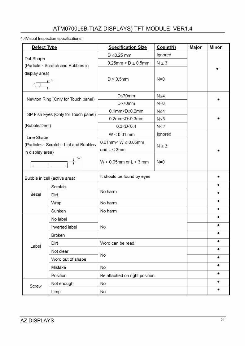
4.4Visual Inspection specifications:

ATM0700L6B-T(AZ DISPLAYS) TFT MODULE VER1.4
AZ DISPLAYS 22
Note: Extraneous substance and scratch not affecting the display of image, for instance, extraneous substanceunder polarizer film but outside the display area, or scratch on metal bezel and backlight module or polarizer filmoutside the display area, shall not be considered as defective or non-conforming.
Top Related