


Languages
Pages
Legal


Direct synthesis procedure for sub-harmonicstub band-pass and band-stop filters
T. Stander, S. Sinha
Carl and Emily Fuchs Institute for MicroelectronicsDepartment of Electrical, Electronic and Computer Engineering
University of Pretoriac/o Lynnwood and University Road
Pretoria, 0002South Africa
E-mail: [email protected]
Abstract: A non-iterative synthesis procedure for sub-harmonic stub (SHS) band-
pass and band-stop filters is presented. The method ensures better agreement
between the synthesized filter response and the original prototype function than was
possible previously without iterative techniques. The procedure is illustrated for two
L-band microstrip filters, with good agreement between modeled and measured
responses.
Keywords: Microstrip filters, transmission line filters, filter synthesis
Introduction: With the advent of miniaturized satellite systems such as the CubeSat
standard, multi-layer and compact system-in-package (SIP) microwave front-ends
require filter topologies with minimum filter order and complexity, yet increasing
selectivity. Finite transmission zeros in filters are used both for increasing pass-band
selectivity [1] and creating wide stop-bands [2]. These zeros are typically realized
with cross-coupled elements [3, 4], multiple mode resonators [5] or multiple
transmission paths [6], all of which add to the filter’s order, size and synthesis
complexity.

A simple transmission line topology for realizing transmission zeros in both band-stop
and band-pass filters was proposed [7, 8] whereby a conventional stub filter’s shunt
stubs were elongated to 2l1 and 4l1 to form sub-harmonic stubs (SHS), where l1 is the
conventional λ0/4 length of a stub generated by Richard’s transform [1] at a given
stop-band or pass-band center frequency f0. In both cases, the authors relied on
iteratively selected, rather than synthesized, values of impedance for the elongated
stubs. This paper presents a synthesis procedure whereby an arbitrary frequency
may be chosen to match the responses of the SHS filter and the original low-pass
prototype response, thereby establishing a non-iterative synthesis method for this
class of filters. This agreement may be used to preserve pass-band reflection, width
or any other chosen parameter through the synthesis process. The process is
demonstrated on both band-pass and band-stop filters.
Band-pass synthesis procedure: The filter synthesis starts as per the traditional
method for synthesizing short- and open-circuited stub filters [1]. The parameters
selected for the Chebyshev filter were N = 3 with 325 MHz transmission bandwidth
around f0 = 1 GHz and 0.5 dB pass-band transmission ripple. Using the transform
Ωc = tan((π fc)/(2f0)) (1)
the cut-off in the low-pass prototype is calculated as 3.832 Rad/s, leading (though
low-pass to high-pass transformation and Richard’s transforms) to the generalized
circuit in Fig. 1 with block “A” representing a short circuit and “B” an open circuit
termination. The response of the prototype function is marked as trace –Δ– in Fig. 2
with synthesized values of Z2 = 219.8 Ω, Z1,3 = 12.65 Ω and f1,2,3 = 1 GHz.
To realize the finite transmission zeros in the stop-band the short-circuited
terminations of the shunt stubs (marked “A” in Fig. 1) are replaced by open-circuited
terminations, and the stubs Z1 and Z3 elongated. The impedance value of these SHS
lines are calculated by considering the input impedance of the original shunt
inductance L in the low-pass prototype
Zin(L) = jΩmL (2)
at any given Richards’ variable value Ωm, which transforms uniquely to a given real
frequency fm. The input impedance of the open-circuit stub, at this frequency, is
calculated as
Zin(Stub) = -jZlcot((πfm)/(2fz)) (3)
where fz is the frequency where the stub’s length is equal to λz/4. A frequency fm of
exact correspondence may now be chosen, which will produce a unique impedance
value Zl for the stub by equating Eq. (2) and Eq. (3). The difference in choosing fm in
the band (0.9 GHz) or at the band edge (0.837 GHz) is shown in Fig. 2. It is observed
that the in-band choice at 0.9 GHz achieves a better transmission band
approximation to the original Chebyshev prototype function, and is chosen for
manufacturing. The value of Z2 remains unchanged from the initial synthesis, with Z2
= 79 Ω, Z3 = 27 Ω, f1 = 0.25 GHz and f3 = 0.5 GHz. To avoid having to manufacture
an impractically high 219.8 Ω stub impedance or uniplanar short-circuited series
stubs [9], the central open-circuit stub is divided into a cascade combination of two
109.9 Ω stubs (Fig. 3, with “A” representing open-circuited terminations). This split
does, however, introduce a short but unavoidable section of transmission line Z4.
Band-stop synthesis procedure: Initial synthesis of the filter is identical to the method
illustrated for band-pass filters, with the parameters of the Chebyshev prototype
function chosen as N = 3, 0.5 dB pass-band transmission ripple and cut-off frequency
fc = 0.163 GHz. The transformed Richards variable is calculated in Eq. (1) as 0.261
Rad/s, leading to the same generalized circuit shown in Fig. 1. In the case of the
band-stop filter, “A” represents an open-circuited termination, whilst “B” represents a
short circuit. The synthesized element values are Z2 = 219.8 Ω, Z1,3 = 12.65 Ω and
f1,2,3 = 1 GHz. The circuit response is shown as the trace marked –Δ– in Fig. 4.
In the band-stop case, instead of calculating the appropriate impedance from a shunt
inductor as in Eq. (2), the impedance of the two elongated stubs are calculated from
the equivalent input impedance of a shunt capacitance C in the lumped element low-
pass prototype
Zin(C) = -j/(ΩmC) (4)
at a given Richards’ variable value Ωm, which transforms to a given real frequency fm.
This impedance is again equated to that of an an open-circuited shunt stub as in Eq.
(3), yielding a unique impedance value for a given fm. The result of choosing fm at the
band center (0.1 GHz) and band edge (0.163 GHz) are illustrated in Fig. 4. The
former achieves a better approximation to the original Chebyshev prototype function
in-band, and is selected for manufacturing. The value of Z2 remains unchanged from
the initial synthesis, with Z1 = 58 Ω, Z3 = 26 Ω, f1 = 0.25 GHz and f3 = 0.5 GHz. As
with the band-pass filter, the 219.8 Ω stub is replaced by two 109.9 Ω stubs
separated by a short section of transmission line, producing the same circuit model
as in Fig. 3 but with “A” representing a short-circuited termination in the case of a
band-stop filter.
Simulation and measurement results: Both filters were realized on two layers of 32mil
Rogers RO4003C, as dimensioned in Fig. 5 and pictured in Fig. 6. For both the band-
pass and band-stop filters, the light shaded trace is the filter’s top signal layer forming
the two series stubs Z2 in Fig. 3. In the band-stop filter’s case, the top strip is
terminated with a via down to the lower signal layer, whilst in the band-pass filter
these vias and via pads are omitted.
The band-pass filter is dimensioned (Fig. 5) as w0 = 1.5, w1 = 1.86, w2 = 0.86, w3 =
6.29, l1 = 169.01, l2 = 91.86, l3 = 82.7 and s = 9.44. The previously noted Z4 is
created by the physical separation between the two stubs on the upper signal layer
(dimensioned s in Fig. 5), and causes some discrepancy between the original circuit
response and the simulated response. This effect is modeled by a line of length λ/4
at 0.8 GHz and impedance 109.93 Ω. The measured results (Fig. 7) were found to
be in good agreement with the simulated response. The final filter features 0.6 dB
mid-band insertion loss and -10 dB input match over a 280 MHz band centered at 1
GHz, with minimum out-of-band attenuation of -22 dB from DC to 4 GHz.
The band-stop filter is dimensioned (in mm, as shown in Fig. 5) as dvia = 0.25 mm, w0
= 1.5, w1 = 1.12, w2 = 0.4, w3 = 4.15, l1 = 164.25, l2 = 90.4, l3 = 80.6, dpad = 0.5 and s
= 2.63. The responses in Fig. 7 show a pole created near f0 due to the presence of
the transmission line of length s on the upper signal layer. This is replicated in the
circuit model (Fig. 8) with a transmission line of Z4 = 109.9 Ω and f4 = 2.3 GHz.
Despite this unwanted circuit element, the filter exhibits -20 dB attenuation over the
stop-band and below 0.1 dB pass-band ripples on either side of the stop-band, with
the evenly spaced finite transmission zeros clearly visible.
Conclusion: A non-iterative synthesis process has been demonstrated for sub-
harmonic stub band-stop and band-pass filters. The method has been demonstrated
to produce filters with realizable impedance values that follow the input reflection
response of the original prototype function better than was previously possible. The
method suffers from some performance degradation due to unwanted additional

transmission lines in physical realization, but good agreement between circuit
simulation and measured results are still obtained if these lines are taken into
account in modeling.
Acknowledgments: The authors wish to thank CST AG for the use of CST Microwave
Studio 2012 under the educational license provided, as well as Denel Dynamics (a
division of Denel (SOC) Ltd.) for measurement facilities. This work was supported by
the National Research Foundation of South Africa (Grant ID# 73666).
References
1 R. J. Cameron, R. R. Mansour, and C. M. Kudsia, Microwave filters for
communication systems, John Wiley & Sons Inc., 2007.
2 M. Sanchez-Soriano, G. Torregrosa-Penalva, and E. Bronchalo, Compact
wideband bandstop filter with four transmission zeros, IEEE Microw Wirel Compon
Lett 20 (2010), 313–315.
3 V. Radonic, and V. Crnojevic-Bengin, Cross-coupled microstrip filter using
grounded patch resonators, Proc 41st European Microwave Conf (2011), 763–766.
4 A. B. Guntupalli, V. K. Velidi, and S. Sanyal, Compact dual wide bandstop filter,
Proc Applied Electromagnetics Conf (2009), 1–4.
5 B. Li, X. Wu, and W. Wu, A miniaturized branch-line coupler with wideband
harmonics suppression, Progress in Electromagnetics Research 17 (2010), 181–189.

6 K. Divyabramham, M. K. Mandal, and S. Sanyal, Sharp-rejection wideband
bandstop filters, IEEE Microw Wirel Compon Lett 18 (2008), 662–664.
7 J. A. G. Malherbe, Wideband bandstop filter with sub-harmonic stubs, Electron Lett
47 (2011), 604–605.
8 J. A. G. Malherbe, Pseudo-elliptic bandpass filter with subharmonic stubs, Electron
Lett 47 (2011), 196–198.
9 T. M. Weller, K. J. Herrick, and L. P. B. Katehi, Bandstop series stubs for coplanar
waveguide on GaAs, Electron Lett 33 (1997), 684 – 685.

Figure captions
Fig. 1 Generalized circuit model of initial SHS filters.
Fig. 2 Circuit model responses of band-pass filter
-Δ- Initial stub filter
-O- SHS filter, fm = 0.837 GHz
-×- SHS filter, fm = 0.9 GHz
Fig. 3 Generalized expanded circuit model of SHS filters.
Fig. 4 Circuit model responses of band-stop filters
-Δ- Initial stub filter
-O- SHS filter, fm = 0.1 GHz
-×- SHS filter, fm = 0.163 GHz
Fig. 5 Microstrip layout of SHS filters. Shaded area is upper signal layer, white outline is lower signallayer.
Fig. 6 Photographs of manufactured band-pass (top) and band-stop (bottom) filters.
Fig. 7 Simulated and measured SHS band-pass filter responses compared to circuit response.
-Δ- Circuit model response, Z4 added.
-O- Simulated response.
-×- Measured response.
Fig. 8 Simulated and measured responses of SHS band-stop filter compared to circuit response.
-Δ- Simulated response.
-O- Circuit model response, Z4 added.
-×- Measured response.

Z2, Θ=90° @ f2
Z1, Θ=90° @ f1 Z3, Θ=90° @ f3
�
� �
Figure 1

Figure 2

Z2, Θ=90° @ f2
Z1, Θ=90° @ f1 Z3, Θ=90° @ f3
Z2, Θ=90° @ f2
Z4, Θ=90° @ f4
� �Figure 3
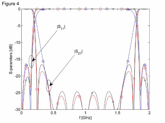
Figure 4
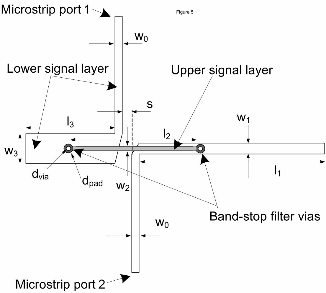
l3
l1
l2w3
w1
w2
w0
w0
s
dvia dpad
Microstrip port 1
Microstrip port 2
Lower signal layer Upper signal layer
Band-stop filter vias
Figure 5
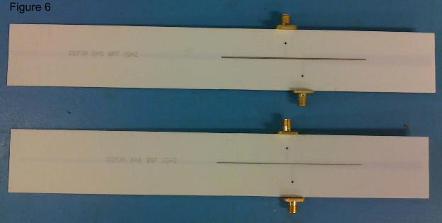
Figure 6
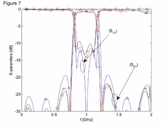
Figure 7

Figure 8
Top Related