


Languages
Pages
Legal


DIGITAL DESIGN USING VERILOG
D. KHALANDAR BASHA, ASSOC. PROF., IARE Page 1
DIGITAL DESIGN using VERILOG
Prepared by:
D. KHALANDAR BASHA
DIGITAL DESIGN USING VERILOG
D. KHALANDAR BASHA, ASSOC. PROF., IARE Page 2
UNIT - 1
INTRODUCTION TO VERILOG:
Verilog as HDL, Levels of design Description, Concurrency, Simulation and Synthesis, Functional
Verification, System Tasks, Programming Language Interface (PLI), Module, Simulation and Synthesis
Tools, Test Benches.
LANGUAGE CONSTRUCTS AND CONVENTIONS:
Introduction, Keywords, Identifiers, White Space Characters, Comments, Numbers, Strings, Logic Values,
Strengths, Data Types, Scalars and Vectors, Parameters, Operators.

DIGITAL DESIGN USING VERILOG
D. KHALANDAR BASHA, ASSOC. PROF., IARE Page 3
VERILOG AS AN HDL
Verilog aimed at providing a functionally tested and a verified design description for the target FPGA or
ASIC. The language has a dual function – one fulfilling the need for a design description and the other
fulfilling the need for verifying the design for functionality and timing constraints like propagation delay,
critical path delay, slack, setup, and hold times
LEVELS OF DESIGN DESCRIPTION
1. Circuit Level:
At the circuit level, a switch is the basic element with which digital circuits are built. Switches can be
combined to form inverters and other gates at the next higher level of abstraction. Verilog has the basic
MOS switches built into its constructs, which can be used to build basic circuits like inverters, basic logic
gates, simple 1-bit dynamic and static memories
2. Gate Level :-
At the next higher level of abstraction, design is carried out in terms of basic gates. All the basic gates are
available as ready modules called “Primitives.” Each such primitive is defined in terms of its inputs and
outputs. Primitives can be incorporated into design descriptions directly.
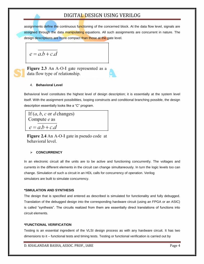
3. Data Flow :-
Data flow is the next higher level of abstraction. All possible operations on signals and variables are
represented here in terms of assignments. All logic and algebraic operations are accommodated. The
DIGITAL DESIGN USING VERILOG
D. KHALANDAR BASHA, ASSOC. PROF., IARE Page 4
assignments define the continuous functioning of the concerned block. At the data flow level, signals are
assigned through the data manipulating equations. All such assignments are concurrent in nature. The
design descriptions are more compact than those at the gate level.
4. Behavioral Level
Behavioral level constitutes the highest level of design description; it is essentially at the system level
itself. With the assignment possibilities, looping constructs and conditional branching possible, the design
description essentially looks like a “C” program.
CONCURRENCY
In an electronic circuit all the units are to be active and functioning concurrently. The voltages and
currents in the different elements in the circuit can change simultaneously. In turn the logic levels too can
change. Simulation of such a circuit in an HDL calls for concurrency of operation. Verilog
simulators are built to simulate concurrency.
*SIMULATION AND SYNTHESIS
The design that is specified and entered as described is simulated for functionality and fully debugged.
Translation of the debugged design into the corresponding hardware circuit (using an FPGA or an ASIC)
is called “synthesis”. The circuits realized from them are essentially direct translations of functions into
circuit elements.
*FUNCTIONAL VERIFICATION
Testing is an essential ingredient of the VLSI design process as with any hardware circuit. It has two
dimensions to it – functional tests and timing tests. Testing or functional verification is carried out by

DIGITAL DESIGN USING VERILOG
D. KHALANDAR BASHA, ASSOC. PROF., IARE Page 5
setting up a “test bench” for the design. The test bench will have the design instantiated in it; it will
generate necessary test signals and apply them to the instantiated design.
Test Inputs for Test Benches:
Any digital system has to carry out a number of activities in a defined manner. Once a proper design is
done, it has to be tested for all its functional aspects. Test inputs can be purely combinational, periodic,
numeric sequences, random inputs, conditional inputs, or combinations of these. As the circuit design
proceeds, one develops smaller blocks and groups them together to form bigger circuit units. The process
is repeated until the whole system is fully built up. Every stage calls for tests to see whether the
subsystem at that layer behaves in the manner expected.
Such testing calls for two types of observations:
� Study of signals within a small unit when test inputs are given to the whole unit.
� Isolation of a small element and doing local test to facilitate debugging.
Constructs for Modeling Timing Delays
Any basic gate has propagation delays and transmission delays associated with it. As the elements in the
circuit increase in number, the type and variety of such delays increase rapidly; often one reaches a stage
where the expected function is not realized thanks to an unduly large time delay.
Verilog has constructs for modeling the following delays:
� Gate delay
� Net delay
� Path delay
� Pin-to-pin delay
A design can be tested for setup time, hold time, clock-width time specifications, etc. Such constructs or
delay models are akin to the finite delay time, rise time, fall time, path or propagation delays, etc.,
associated with real digital circuits or systems. The use of such constructs in the design helps simulate
realistic conditions in a digital circuit.
SYSTEM TASKS
A number of system tasks are available in Verilog. Though used in a design description, they are not part
of it. Some tasks facilitate control and flow of the testing process. Reading data from specified files into a
module and writing back into files are also possible through other tasks. Timescale can be changed prior
to simulation with the help of specific tasks for the purpose.
A set of system functions add to the flexibility of test benches: They are of three categories:
� Functions that keep track of the progress of simulation time
DIGITAL DESIGN USING VERILOG
D. KHALANDAR BASHA, ASSOC. PROF., IARE Page 6
� Functions to convert data or values of variables from one format to another
� Functions to generate random numbers with specific distributions
PROGRAMMING LANGUAGE INTERFACE (PLI)
PLI provides an active interface to a compiled Verilog module. The interface adds a new dimension to
working with Verilog routines from a C platform.
The key functions of the interface are as follows:
� One can read data from a file and pass it to a Verilog module as input. Such data can be test
vectors or other input data to the module. Similarly, variables in Verilog modules can be accessed
and their values written to output devices.
� Delay values, logic values, etc., within a module can be accessed and altered.
� Blocks written in C language can be linked to Verilog modules.
* MODULE
Any Verilog program begins with a keyword – called a “module.” A module is the name given to any
system considering it as a black box with input and output terminals The terminals of the module are
referred to as ‘ports’.
The ports attached to a module can be of three types:
� input ports through which one gets entry into the module; they signify the input signal terminals
of the module.
� output ports through which one exits the module; these signify the output signal terminals of
the module.
� inout ports: These represent ports through which one gets entry into the module or exits the
module; These are terminals through which signals are input to the module sometimes; at some
other times signals are output from the module through these.
Verilog takes the active statements appearing between the “module” statement and the “endmodule”
statement.
* SIMULATION AND SYNTHESIS

DIGITAL DESIGN USING VERILOG
D. KHALANDAR BASHA, ASSOC. PROF., IARE Page 7
UNIT - II GATE LEVEL MODELING
AND Gate Primitive, Module Structure, Other Gate
Primitives
Illustrative Examples
Tri-State Gates, Array of Instances of Primitives
Design of Flip-flops with Gate Primitives, Delays
Strengths and Contention Resolution
Net Types, Design of Basic Circuits
MODULE STRUCTURE
The first statement of a module starts with the keyword module; it may be followed by the name
of the module and the port list if any. All the variables in the ports-list are to be identified as inputs,
outputs, or inouts.
The corresponding declarations have the form shown below:
Input a1, a2;
Output b1, b2;
Inout c1, c2;
The port-type declarations here follow the module declaration mentioned above. The ports and
the other variables used within the body of the module are to be identified as nets or registers with
specific types in each case.
The respective declaration statements follow the port-type declaration statements.
Examples: wire a1, a2, c;
reg b1, b2;
The type declaration must necessarily precede the first use of any variable or signal in the module.
The executable body of the module follows the declaration indicated above.
The last statement in any module definition is the keyword “endmodule”.
Comments can appear anywhere in the module definition.
AND GATE PRIMITIVE
The AND gate primitive in Verilog is instantiated with the following statement:
and g1 (O, I1, I2, . . ., In);
The AND module has only one output. The first port in the argument list is
the output port.

DIGITAL DESIGN USING VERILOG
D. KHALANDAR BASHA, ASSOC. PROF., IARE Page 8
An AND gate instantiation can take any number of inputs — the upper limit is
compiler-specific.
A name need not be necessarily assigned to the AND gate instantiation; this is
true of all the gate primitives available in Verilog.
Truth Table of AND Gate Primitive
OTHER GATE PRIMITIVES
Basic gate primitives in Verilog with details
In all cases of instantiations, one need not necessarily assign a name to the instantiation. It need be done
only when felt necessary – say for clarity of circuit description.
In all the cases the output port(s) is (are) declared first and the input port(s) is (are) declared
subsequently.
The buffer and the inverter have only one input each. They can have any number of outputs; the
upper limit is compiler-specific.
All other gates have one output each but can have any number of inputs; the upper limit is again
compiler-specific.

DIGITAL DESIGN USING VERILOG
D. KHALANDAR BASHA, ASSOC. PROF., IARE Page 9
Rules for deciding the output values of gate primitives for different input combinations
Example programs
module aoi_gate(o,a1,a2,b1,b2);
input a1,a2,b1,b2; // a1,a2,b1,b2 form the input ports of the module
output o; //o is the single output port of the module
wire o1,o2; //o1 and o2 are intermediate signals within the module
and g1(o1,a1,a2); //The AND gate primitive has two
and g2(o2,b1,b2); // instantiations with assigned names g1 & g2.
nor g3(o,o1,o2); //The nor gate has one instantiation with assigned name g3.
endmodule
DIGITAL DESIGN USING VERILOG
D. KHALANDAR BASHA, ASSOC. PROF., IARE Page 10
//Test-bench for the aoi_gate above
module aoi_st;
reg a1,a2,b1,b2; //specific values will be assigned to a1,a2,b1 and b2 and these
//connected to input ports of the gate insatntiations;
//hence these variables are declared as reg
wire o;
initial
begin
a1 = 0;
a2 = 0;
b1 = 0;
b2 = 0;
#3 a1 = 1;
#3 a2 = 1;
#3 b1 = 1;
#3 b2 = 0;
#3 a1 = 1;
#3 a2 = 0;
#3 b1 = 0;
end
initial #100 $stop; //the simulation ends after running for 100 tu's.
initial $monitor($time , " o = %b , a1 = %b , a2 = %b , b1 = %b ,b2 = %b ",o,a1,a2,b1,b2);
aoi_gate gg(o,a1,a2,b1,b2);
endmodule
EX 2-to-4 Decoder
module dec2_4 (a,b,en);
output [3:0] a;
input [1:0]b;
input en;
wire [1:0]bb;
not(bb[1],b[1]),(bb[0],b[0]);
and(a[0],en, bb[1],bb[0]),(a[1],en, bb[1],b[0]),(a[2],en, b[1],bb[0]),(a[3],en, b[1],b[0]);
endmodule
DIGITAL DESIGN USING VERILOG
D. KHALANDAR BASHA, ASSOC. PROF., IARE Page 11
//test bench
module tst_dec2_4();
wire [3:0]a;
reg[1:0] b; reg en;
dec2_4 dec(a,b,en);
initial
begin
{b,en} =3'b000;
#2{b,en} =3'b001;
#2{b,en} =3'b011;
#2{b,en} =3'b101;
#2{b,en} =3'b111;
end
initial
$monitor ($time , "output a = %b, input b = %b ", a, b);
endmodule
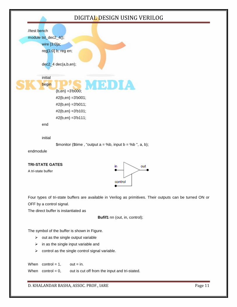
TRI-STATE GATES
A tri-state buffer
Four types of tri-state buffers are available in Verilog as primitives. Their outputs can be turned ON or
OFF by a control signal.
The direct buffer is instantiated as
Bufif1 nn (out, in, control);
The symbol of the buffer is shown in Figure.
out as the single output variable
in as the single input variable and
control as the single control signal variable.
When control = 1, out = in.
When control = 0, out is cut off from the input and tri-stated.

DIGITAL DESIGN USING VERILOG
D. KHALANDAR BASHA, ASSOC. PROF., IARE Page 12
The output, input and control signals should appear in the instantiation in the same order as above.
Details of bufif1 as well as the other tri-state type primitives are shown in Table. In all the cases shown in
Table, out is the output, in is the input, and control, the control variable.
Instantiation and functional details of tri-state buffer primitives
The following observations are common to all the tri-state buffer primitives:
If the control signal has a value that corresponds to the buffer being on, two possibilities exist:
The output has the same value as the input if the input is 0 or 1.
The output is at x otherwise (i.e., if the input is x or z).
If the control signal has a value that corresponds to the control signal being off, the output is at z
state irrespective of the value of the input.
If the control signal is at x or z, three possibilities arise:
If the input is at x or z, the output is at x.
If the input is at 0 state, the output is L for bufif1 and bufif0. It is at H for notif1 and notif0.
If the input is at 1 state, the output is H for bufif1 and bufif0. It is at L for notif1 and notif0.
Note that H corresponds to 1 or z state while L corresponds to 0 or z state
DIGITAL DESIGN USING VERILOG
D. KHALANDAR BASHA, ASSOC. PROF., IARE Page 13
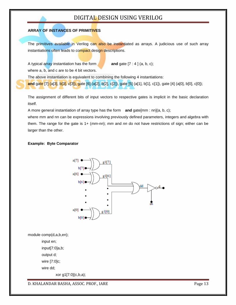
ARRAY OF INSTANCES OF PRIMITIVES
The primitives available in Verilog can also be instantiated as arrays. A judicious use of such array
instantiations often leads to compact design descriptions.
A typical array instantiation has the form and gate [7 : 4 ] (a, b, c);
where a, b, and c are to be 4 bit vectors.
The above instantiation is equivalent to combining the following 4 instantiations:
and gate [7] (a[3], b[3], c[3]), gate [6] (a[2], b[2], c[2]), gate [5] (a[1], b[1], c[1]), gate [4] (a[0], b[0], c[0]);
The assignment of different bits of input vectors to respective gates is implicit in the basic declaration
itself.
A more general instantiation of array type has the form and gate[mm : nn](a, b, c);
where mm and nn can be expressions involving previously defined parameters, integers and algebra with
them. The range for the gate is 1+ (mm-nn); mm and nn do not have restrictions of sign; either can be
larger than the other.
Example: Byte Comparator
module comp(d,a,b,en);
input en;
input[7:0]a,b;
output d;
wire [7:0]c;
wire dd;
xor g1[7:0](c,b,a);

DIGITAL DESIGN USING VERILOG
D. KHALANDAR BASHA, ASSOC. PROF., IARE Page 14
or(dd,c);
notif1(d,dd,en);
endmodule
Test Bench for comparator
module comp_tb;
reg[7:0]a,b;
reg en;
comp gg(d,a,b,en);
initial
begin
a = 8'h00;
b = 8'h00;
en = 1'b0;
end
always
#2 en = 1'b1;
always
begin
#2 a = a+1'b1;
#2 b = b+2'd2;
end
initial $monitor($time," en = %b , a = %b ,b = %b ,d = %b ",en,a,b,d);
initial #30 $stop;
endmodule
half adder
module ha(s,ca,a,b);
input a,b;
output s,ca;
xor(s,a,b);
and(ca,a,b);
endmodule

DIGITAL DESIGN USING VERILOG
D. KHALANDAR BASHA, ASSOC. PROF., IARE Page 15
//test-bench
module tstha();
reg a,b;
wire s,ca;
ha hh(s,ca,a,b);
initial
begin
a=0;b=0;
end
always
begin
#2 a=1;b=0;
#2 a=0;b=1;
#2 a=1;b=1;
#2 a=0;b=0;
end
initial $monitor($time , " a = %b , b = %b ,out carry = %b , outsum = %b " ,a,b,ca,s);
initial #24 $stop;
endmodule
Full adder
module fa(sum,cout,a,b,cin);
input a,b,cin;
output sum,cout;
wire s,c1,c2;

DIGITAL DESIGN USING VERILOG
D. KHALANDAR BASHA, ASSOC. PROF., IARE Page 16
ha ha1(s,c1,a,b), ha2(sum,c2,s,cin);
or(cout,c2,c1);
endmodule
//test-bench
module tst_fa();
reg a,b,cin;
fa ff(sum,cout,a,b,cin);
initial
begin
a =0;b=0;cin=0;
end
always
begin
#2 a=1;b=1;cin=0;#2 a=1;b=0;cin=1;
#2 a=1;b=1;cin=1;#2 a=1;b=0;cin=0;
#2 a=0;b=0;cin=0;#2 a=0;b=1;cin=0;
#2 a=0;b=0;cin=1;#2 a=0;b=1;cin=1;
#2 a=1;b=0;cin=0;#2 a=1;b=1;cin=0;
#2 a=0;b=1;cin=0;#2 a=1;b=1;cin=1;
end
initial $monitor($time ," a = %b, b = %b, cin = %b, outsum = %b, outcar = %b ", a,b,cin,sum,cout);
initial #30 $stop ;
endmodule

DIGITAL DESIGN USING VERILOG
D. KHALANDAR BASHA, ASSOC. PROF., IARE Page 17
Mux
module mux4_1(y,i,s);
input [3:0] i;
input [1:0] s;
output y;
wire [1:0] ss;
wire [3:0]yy;
not (ss[0],s[0]),(ss[1],s[1]);
and (yy[0],i[0],ss[0],ss[1]);
and (yy[1],i[1],s[0],ss[1]);
and (yy[2],i[2],ss[0],s[1]);
and (yy[3],i[3],s[0],s[1]);
or (y,yy[3],yy[2],yy[1],yy[0]);
endmodule
//test-bench
module tst_mux4_1();
reg [3:0]i;
reg [1:0] s;
mux4_1 mm(y,i,s);
initial
begin
#2{i,s} = 6'b 0000_00;
#2{i,s} = 6'b 0001_00;
#2{i,s} = 6'b 0010_01;
#2{i,s} = 6'b 0100_10;
#2{i,s} = 6'b 1000_11;
#2{i,s} = 6'b 0001_00;
end
initial
$monitor($time," input s = %b,y = %b" ,s,y);
Endmodule

DIGITAL DESIGN USING VERILOG
D. KHALANDAR BASHA, ASSOC. PROF., IARE Page 18
DESIGN OF FLIP-FLOPS WITH GATE PRIMITIVES
The basic RS latch can be designed using gate primitives. Two instantiations of NAND or NOR gates
suffice here.
A Simple Latch
The design description of a simple latch formed with two NAND gates as follows
module sbrbff(sb,rb,q,qb);
input sb,rb;
output q,qb;
nand(q,sb,qb);
nand(qb,rb,q);
endmodule
Test Bench of simple latch
module tstsbrbff; //test-bench
reg sb,rb;
wire q,qb;
sbrbff ff(sb,rb,q,qb);
initial
begin
sb =1'b1;
rb =1'b0;
end
always
begin
#2 sb =1'b1;rb =1'b1;
#2 sb =1'b0;rb =1'b1;
#2 sb =1'b1;rb =1'b1;
#2 sb =1'b1;rb =1'b0;
#2 sb =1'b1;rb =1'b1;
end
initial $monitor($time, " sb = %b, rb = %b, q = %b, qb = %b",sb,rb,q,qb);
DIGITAL DESIGN USING VERILOG
D. KHALANDAR BASHA, ASSOC. PROF., IARE Page 19
initial #20 $stop;
endmodule
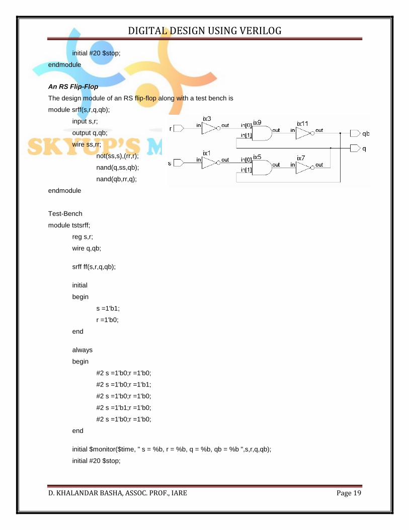
An RS Flip-Flop
The design module of an RS flip-flop along with a test bench is
module srff(s,r,q,qb);
input s,r;
output q,qb;
wire ss,rr;
not(ss,s),(rr,r);
nand(q,ss,qb);
nand(qb,rr,q);
endmodule
Test-Bench
module tstsrff;
reg s,r;
wire q,qb;
srff ff(s,r,q,qb);
initial
begin
s =1'b1;
r =1'b0;
end
always
begin
#2 s =1'b0;r =1'b0;
#2 s =1'b0;r =1'b1;
#2 s =1'b0;r =1'b0;
#2 s =1'b1;r =1'b0;
#2 s =1'b0;r =1'b0;
end
initial $monitor($time, " s = %b, r = %b, q = %b, qb = %b ",s,r,q,qb);
initial #20 $stop;

DIGITAL DESIGN USING VERILOG
D. KHALANDAR BASHA, ASSOC. PROF., IARE Page 20
endmodule
A Clocked RS Flip-Flop
module srffcplev(cp,s,r,q,qb);
input cp,s,r;
output q,qb;
wire ss,rr;
nand(ss,s,cp),(rr,r,cp),(q,ss,qb),(qb,rr,q);
endmodule
Test-Bench
module srffcplev_tst;
reg cp,s,r;
wire q,qb;
srffcplev ff(cp,s,r,q,qb);
initial
begin
cp=1'b0;
s =1'b1;
r =1'b0;
end
always #2cp=~cp;
always
begin
#4 s =1'b0;r =1'b0;
#4 s =1'b0;r =1'b1;
#4 s =1'b0;r =1'b0;
#4 s =1'b1;r =1'b0;
#4 s =1'b0;r =1'b0;
end
initial $monitor($time,"cp = %b ,s = %b , r = %b , q = %b , qb = %b " ,cp,s,r,q,qb);
initial #20 $stop;
DIGITAL DESIGN USING VERILOG
D. KHALANDAR BASHA, ASSOC. PROF., IARE Page 21
endmodule
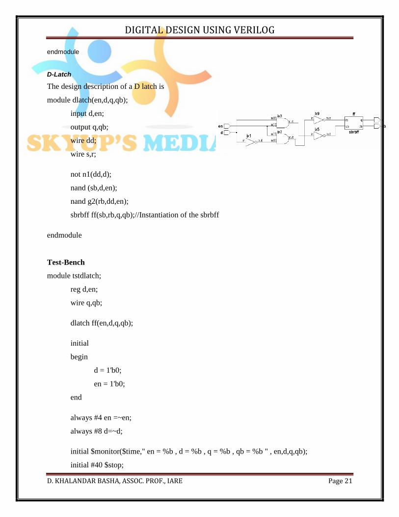
D-Latch
The design description of a D latch is
module dlatch(en,d,q,qb);
input d,en;
output q,qb;
wire dd;
wire s,r;
not n1(dd,d);
nand (sb,d,en);
nand g2(rb,dd,en);
sbrbff ff(sb,rb,q,qb);//Instantiation of the sbrbff
endmodule
Test-Bench
module tstdlatch;
reg d,en;
wire q,qb;
dlatch ff(en,d,q,qb);
initial
begin
d = 1'b0;
en = 1'b0;
end
always #4 en =~en;
always #8 d=~d;
initial $monitor($time," en = %b , d = %b , q = %b , qb = %b " , en,d,q,qb);
initial #40 $stop;

DIGITAL DESIGN USING VERILOG
D. KHALANDAR BASHA, ASSOC. PROF., IARE Page 22
endmodule
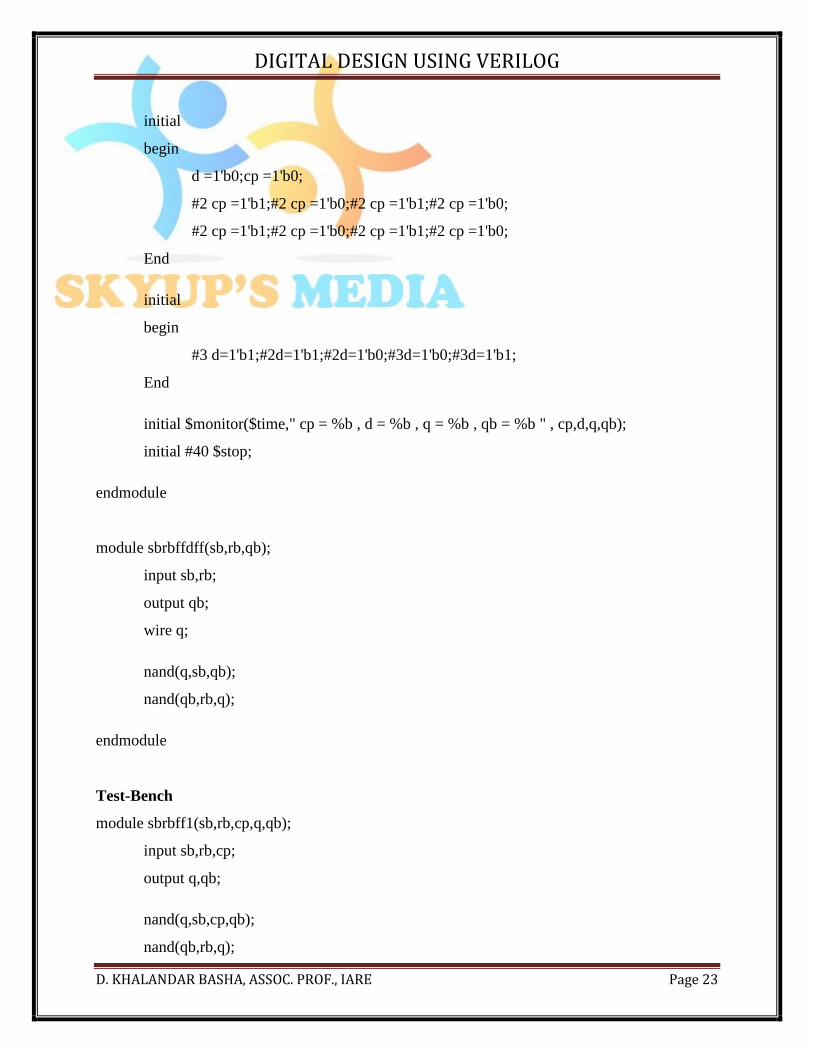
An Edge-Triggered Flip-Flop
Figure shows the circuit of an edge-triggered flip-flop.
module dffgatnew1(cp,d,q,qb);
input d,cp;
output q,qb;
wire sb,rb;
wire s,r;
sbrbffdff ff1(rb,cp,s);
sbrbff1 ff2(s,d,cp,r,rb);
sbrbff ff3(s,r,q,qb);
endmodule
Test-Bench
module tst_dffgatnew1;
reg d,cp;
wire q,qb;
dffgatnew1 ff(cp,d,q,qb);
DIGITAL DESIGN USING VERILOG
D. KHALANDAR BASHA, ASSOC. PROF., IARE Page 23
initial
begin
d =1'b0;cp =1'b0;
#2 cp =1'b1;#2 cp =1'b0;#2 cp =1'b1;#2 cp =1'b0;
#2 cp =1'b1;#2 cp =1'b0;#2 cp =1'b1;#2 cp =1'b0;
End
initial
begin
#3 d=1'b1;#2d=1'b1;#2d=1'b0;#3d=1'b0;#3d=1'b1;
End
initial $monitor($time," cp = %b , d = %b , q = %b , qb = %b " , cp,d,q,qb);
initial #40 $stop;
endmodule
module sbrbffdff(sb,rb,qb);
input sb,rb;
output qb;
wire q;
nand(q,sb,qb);
nand(qb,rb,q);
endmodule
Test-Bench
module sbrbff1(sb,rb,cp,q,qb);
input sb,rb,cp;
output q,qb;
nand(q,sb,cp,qb);
nand(qb,rb,q);

DIGITAL DESIGN USING VERILOG
D. KHALANDAR BASHA, ASSOC. PROF., IARE Page 24
endmodule
DELAYS
Verilog has the facility to account for different types of propagation delays of circuit
elements. Any connection can cause a delay due to the distributed nature of its resistance and
capacitance. Similar delays are present in gates too. These manifest as propagation delays in the
0 to 1 transitions and 1 to 0 transitions from input to the output. Such propagation delays can
differ for the two types of transitions.
Net Delay
One of the simplest delays is that of a direct connection – a net.
It can be part of the declaration statement
wire #2 nn; // nn is declared as a net with a propagation delay of 2 time steps
Here nn is declared as a net with an associated propagation delay of 2 time steps. The delay is the
same for the positive as well as the negative transitions. Similar delays can be assigned to other
types of nets as well. Whenever a variable or a signal is defined as a net and no delay is specified
for it, the associated delay is taken as zero.
The impedance connected as well as the type of loading can differ for the two transitions. The
propagation delay too can differ accordingly. Two such delays can be specified as follows:
Wire # (2, 1) nm;
Here nm is declared as a net with two distinct propagation delays; the positive (0 to 1) transition has a
delay of 2 time steps associated with it. The negative (1 to 0) transition has a delay of 1 time step.

DIGITAL DESIGN USING VERILOG
D. KHALANDAR BASHA, ASSOC. PROF., IARE Page 25
Gate Delay
Gates delays can be specified as part of the instantiation itself.
and #3 g ( a, b, c);
The above represents an AND gate description with a uniform delay of 3 ns for all transitions from input to
output. A more detailed description can be as follows:
and #(2, 1) (a, b, c);
With the above statement the positive (0 to 1) transition at the output has a delay of 2 time steps while the
negative (1 to 0) transition has a delay of 1 time step.
In a more detailed design description, delays can be associated with nets as well as gates.
Delays with Tri-state Gates
For tri-state gates the delays associated with the control signals can be different from those of the
input as well as the output.
Three time delay values are specified:
1. The first number represents the delay associated with the positive (0 to 1) transition of the output.
2. The second number represents the delay associated with the negative (1 to 0) transition of the output.
3. The third number represents the delay for the output to go to the hi-Z state as the control signal
changes from 1 to 0 (i.e., ON to OFF command).
DIGITAL DESIGN USING VERILOG
D. KHALANDAR BASHA, ASSOC. PROF., IARE Page 26
Delays for the other tri-state buffers – namely bufif0, notif1 and notif0 – may be specified in a similar manner. The following are noteworthy here:
Delays and storage times can be specified on the gate primitives and the nets but not on regs.
All three time values are separately specified in the most versatile case.
If only two time-values are specified, these are interpreted by Verilog as the rise (0 to 1) and fall
(1 to 0) time, respectively. The turn-off time (delay) is taken as the smaller of these two.
If only one time value is specified, it is taken as the rise time, the fall time, and the turn-off time.
If no time value is specified, the rise and fall times at the output are taken as zero. The turn-off is
taken as instantaneous.
It is customary for manufacturers to specify delays and their range in the following manner:
Max delay: The maximum value of the delay in a batch; that is, the delay encountered in practice
is guaranteed to be less than this in the worst case.
Min. delay: Minimum value of delay in a batch; that is, the specified signal is guaranteed to be
available only after a minimum of time specified.
Typ. delay: Typical or representative value of the delay.
Each of the delays in a gate primitive or for a net can be specified in terms of these three values.
For example and #(2:3:4) g1(a0, a1, a2);
can instantiate an AND gate with the following time delay specifications:
The 0 to 1 rise time and the 1 to 0 fall time are equal.
The minimum value of either is 2 time steps. Typical value is 3 time steps and the maximum
value is 4 time steps.
Note that the colon that separates the numbers signifies that the timings specified are the
minimum, typical, and maximum values.
If the same is not specified, the simulation is carried out with the typical delay value.
The group of minimum, typical, and maximum delay values for the propagation delays can be specified
separately for any gate primitive. Thus an AND gate primitive can be specified as
and #(1:2:3, 2:4:6) g2(b0, b1, b2);
Here for the 0 to 1 transition of the output (rise time) the gate has a minimum delay value of 1 ns, a typical
value of 2 ns, and a maximum value of 3 ns. Similarly, for the 1 to 0 transition (fall time) the gate has a
minimum delay value of 2 ns, a typical delay value of 4 ns, and a maximum delay value of 6 ns. Such
delay specifications can be associated with nets as well as tri-state type gates also.
wire #(1:2:3) a; /* The net a has a propagation delay whose minimum, typical
and maximum values are 1 ns, 2 ns, and 3 ns, respectively*/
bufif1 #(1:2:3, 2:4:6, 3:6:9) g3 (a0, b0, c0);
The different delay values for the buffer are as follows:
DIGITAL DESIGN USING VERILOG
D. KHALANDAR BASHA, ASSOC. PROF., IARE Page 27
The output rise time (0 to 1 transition) has a minimum value of 1 ns, a typical value of 2 ns and a
maximum value of 3 ns.
The output fall time (1 to 0 transition) has a minimum value of 2 ns, a typical value of 4 ns and a
maximum value of 6 ns.
The output turn-off time (1 to 0) has a minimum value of 3 ns, a typical value of 6 ns, and a
maximum value of 9 ns
The following general observations are in order regarding the overall delays through the circuit:
A normal design can have many gates and nets in its signal paths. The delay through any path
for a signal depends on the path and the type of transitions at each stage.
The cumulative delay for a signal in a path puts an upper limit on the maximum operating
frequency vis-à-vis the signal.
A signal may go through multiple paths in a design to arrive at one gate. It is necessary to match
the delays within specified tolerances for reliable operation of the device.
In larger designs, one has to identify the longest signal path (critical path).
This puts an upper limit on the operating frequency apart from causing maloperation in a worst-
case scenario. One of the practices in design is to reroute selected signals or redo selected
design segments to reduce critical path delays.
STRENGTHS AND CONTENTION RESOLUTION
In practical situations, outputs of logic gates and signals on nets in a circuit have associated source
impedances. When the outputs of two gates are joined together, the signal level is decided by the relative
magnitudes of the source impedances.
Strengths of Gate Primitives
Table gives the names associated with strengths, respective abbreviations, and their order by weight.
The strengths associated with the output of a gate primitive can be specified separately for the
two logic levels

DIGITAL DESIGN USING VERILOG
D. KHALANDAR BASHA, ASSOC. PROF., IARE Page 28
Strength Contention in Gate Primitives
When two signals of opposite polarity and differing strengths drive a line, the output status is
decided by the stronger signal. However, if the signals are of equal strength, the output is
indeterminate. Different contention possibilities arise here
Whenever there is a contention, the logic value of the output is decided by the stronger signal.
Net Charges
Whenever a net is driven by a signal, it takes the logic value of the signal. When the signal
source is tri-stated, the net too gets tri-stated. In practice the net can have a capacitor associated
with it, which can store the signal level even after the signal source dries up. To account for this
situation, a charge storage capacity is associated with the net. Such nets are declared with the
keyword trireg.
A trireg net can be in one of two possible states only
Driven state: When driven by a source or multiple sources, the net assumes the strength
of the source. It can be any of the strengths except the high impedance value.
Capacitive state: When the driven source (sources) is (are) tri-stated, the net retains the
last value it was in – by virtue of the capacitance associated with it.
The value can be 0, 1 or x (but not the high impedance value).
When in the capacitive state, a net can have a storage strength associated with it. Three such
storage strengths are possible – namely large, medium, and small
When a storage strength is not specified, it is assigned the default value – medium.
Contention Between Net and Gate Primitive Outputs
In case of a contention between a signal output from a gate and the charge on a net, the
contention is decided by the relative strengths of the signals on each.
Table combines all the strengths
DIGITAL DESIGN USING VERILOG
D. KHALANDAR BASHA, ASSOC. PROF., IARE Page 29
Net Types and Port Assignments
All input ports of modules have to accept inputs from outside when instantiated and respond to
changes in them. Hence they have to be of net type. Note that input ports cannot be of reg type
since their values cannot be changed from outside. The output ports of instantiated modules can
be of net or reg types.
Inout ports have to function as input or output ports; hence they too have to be of net types.
The port assignments in an instantiation can be to scalars, vectors, part vectors, or concatenated
vectors. However, their sizes should match those of the ports in the module definitions. Further,
the type restrictions mentioned above have to be complied with.
NET TYPES
wire is possibly the simplest type of net declaration.
wand and wor Types of Nets
DESIGN OF BASIC CIRCUITS
Example ALU
The ALU considered carries out four functions:
Addition of two 4-bit numbers.
Complementing all the bits of a 4-bit vector.
Bit-by-bit AND operation on two nibbles.
Bit-by-bit XOR operation on two nibbles.
module add4g(sum,carry,a,b,cin);
input[3:0]a,b;
input cin;
output[3:0]sum;
output carry;
wire [2:0]cc;
fa a0(sum[0],cc[0],a[0],b[0],cin);
fa a1(sum[1],cc[1],a[1],b[1],cc[0]);
fa a2(sum[2],cc[2],a[2],b[2],cc[1]);
fa a3(sum[3],carry,a[3],b[3],cc[2]);
endmodule
DIGITAL DESIGN USING VERILOG
D. KHALANDAR BASHA, ASSOC. PROF., IARE Page 30
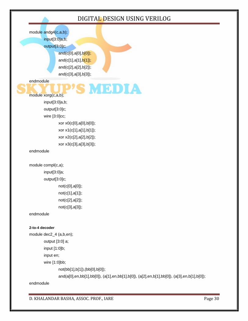
module andg4(c,a,b);
input[3:0]a,b;
output[3:0]c;
and(c[0],a[0],b[0]);
and(c[1],a[1],b[1]);
and(c[2],a[2],b[2]);
and(c[3],a[3],b[3]);
endmodule
module xorg(c,a,b);
input[3:0]a,b;
output[3:0]c;
wire [3:0]cc;
xor x0(c[0],a[0],b[0]);
xor x1(c[1],a[1],b[1]);
xor x2(c[2],a[2],b[2]);
xor x3(c[3],a[3],b[3]);
endmodule
module compl(c,a);
input[3:0]a;
output[3:0]c;
not(c[0],a[0]);
not(c[1],a[1]);
not(c[2],a[2]);
not(c[3],a[3]);
endmodule
2-to-4 decoder
module dec2_4 (a,b,en);
output [3:0] a;
input [1:0]b;
input en;
wire [1:0]bb;
not(bb[1],b[1]),(bb[0],b[0]);
and(a[0],en,bb[1],bb[0]), (a[1],en,bb[1],b[0]), (a[2],en,b[1],bb[0]), (a[3],en,b[1],b[0]);
endmodule

DIGITAL DESIGN USING VERILOG
D. KHALANDAR BASHA, ASSOC. PROF., IARE Page 31
4-to-1 mux module
module mux4_1alu(y,i,e);
input [3:0] i;
input e;
output [3:0]y;
bufif1 g1(y[3],i[3],e);
bufif1 g2(y[2],i[2],e);
bufif1 g3(y[1],i[1],e);
bufif1 g4(y[0],i[0],e);
endmodule
module alu_4g(a,b,c,carry,cin,cen,s);
input [3:0]a,b;
input[1:0]s;
input cen,cin;
output [3:0]c;
output carry;
wire [3:0] data0,data1,data2,data3,e;
wire carry1 ;
dec2_4 m5(e,s,cen);
add4g m1(data0,carry1,a,b,cin);
compl m2(data1,a);
xorg m3(data2,a,b);
andg4 m4(data3,a,b);
bufif1 g5(carry,carry1,cen);
mux4_1alu m6(c,data0,e[0]);
mux4_1alu m7(c,data1,e[1]);
mux4_1alu m8(c,data2,e[2]);
mux4_1alu m9(c,data3,e[3]);
endmodule

DIGITAL DESIGN USING VERILOG
D. KHALANDAR BASHA, ASSOC. PROF., IARE Page 32
UNIT - III BEHAVIORAL MODELING
Introduction
Operations and Assignments
Functional Bifurcation
Initial Construct, Always Construct
Examples, Assignments with Delays
Wait construct, Multiple Always Blocks
Blocking and Non blocking Assignments
The case statement
iƒ and iƒ-else constructs
assigndeassign construct, repeat construct, for loop
the disable construct, while loop, forever loop
parallel blocks, force-release construct, Event
INTRODUCTION
Behavioral level modeling constitutes design description at an abstract level. One can visualize
the circuit in terms of its key modular functions and their behavior; it can be described at a functional level
itself instead of getting bogged down with implementation details.
OPERATIONS AND ASSIGNMENTS
The design description at the behavioral level is done through a sequence of assignments. These are
called ‘procedural assignments’
The procedure assignment is characterized by the following:
The assignment is done through the “=” symbol (or the “<=” symbol) as was the case with the
continuous assignment earlier.
An operation is carried out and the result assigned through the “=” operator to an operand
specified on the left side of the “=” sign – for example, N = ~N; Here the content of reg N is
complemented and assigned to the reg N itself. The assignment is essentially an updating
activity.
The operation on the right can involve operands and operators. The operands can be of different
types – logical variables, numbers – real or integer and so on.
All the operands are given in Tables 6.1 to 6.9. The format of using them and the rules of
precedence remain the same.
The operands on the right side can be of the net or variable type. They can be scalars or vectors.

DIGITAL DESIGN USING VERILOG
D. KHALANDAR BASHA, ASSOC. PROF., IARE Page 33
It is necessary to maintain consistency of the operands in the operation expression –
e.g., N = m / l; Here m and l have to be same types of quantities – specifically a reg,
integer, time, real, realtime, or memory type of data – declared in advance.
The operand to the left of the “=” operator has to be of the variable (e.g., reg) type. It has to be
specifically declared accordingly. It can be a scalar, a vector, a part vector, or a concatenated
vector.
Procedural assignments are very much like sequential statements in C. Normally they are carried
out one at a time sequentially. As soon as a specified operation on the right is carried out, the
result is assigned to the quantity on the left – for example N = m + l; N1 = N * N;
The above form a set of two procedures placed within an always block. Generally they are carried out
sequentially in the order specified
The sequential nature of the assignments requires the operands on the left of the assignment to be of reg
(variable) type.
FUNCTIONAL BIFURCATION
Design description at the behavioral level is done in terms of procedures of two types; one involves
functional description and interlinks of functional units. It is carried out through a series of blocks under an
“always”
The second concerns simulation – its starting point, steering the simulation flow, observing the process
variables, and stopping of the simulation process; all these can be carried out under the “always” banner,
an “initial” banner, or their combinations. However, each always and each initial block initiates an
activity flow during simulation
In general the activity with all such blocks starts at the simulation time and flows concurrently during the
whole simulation process
A procedure-block of either type – initial or Always

DIGITAL DESIGN USING VERILOG
D. KHALANDAR BASHA, ASSOC. PROF., IARE Page 34
Structure of a typical procedural block
begin – end Construct
If a procedural block has only one assignment to be carried out, it can be specified as below:
initial #2 a=0;
If more than one procedural assignment is to be carried out in an initial block. All such assignments are
grouped together between “begin” and “end” declarations.
The following are to be noted here:
Every begin declaration must have its associated end declaration.
begin – end constructs can be nested as many times as desired.

DIGITAL DESIGN USING VERILOG
D. KHALANDAR BASHA, ASSOC. PROF., IARE Page 35
Name of the Block
Any block can be assigned a name, but it is not mandatory. Only the blocks which are to be identified and
referred by the simulator need be named.
Assigning names to blocks serves different purposes:
Registers declared within a block are local to it and are not available outside. However, during
simulation they can be accessed for simulation, etc., by proper dereferencing.
Named blocks can be disabled selectively when desired
Local Variables
Variables used exclusively within a block can be declared within it. Such a variable need not be
declared outside, in the module encompassing the block. Such local declarations conserve memory and
offer other benefits too. Regs declared and used within a block are static by nature. They retain their
values at the time of leaving the block. The values are modified only at the next entry to the block.
INITIAL CONSTRUCT
A set of procedural assignments within an initial construct are executed only once – and, that
too, at the times specified for the respective assignments
The initial process is characterized by the following
In any assignment statement the left-hand side has to be a storage type of element (and not a
net). It can be a reg, integer, or real type of variable. The right-hand side can be a storage type
of variable (reg, integer, or real type of variable) or a net.
All the procedural assignments appear within a begin–end block
All the procedural assignments are executed sequentially – in the same order as they appear in
the design description.
The initial block above does three controlling activities during the simulation run.
Initialize the selected set of reg's at the start.
Change values of reg's at predetermined instances of time. These form the inputs to the
module(s) under test and test it for a desired test sequence.
Stop simulation at the specified time.
Multiple Initial Blocks
A module can have as many initial blocks as desired. All of them are activated at the start of simulation.
The time delays specified in one initial block are exclusive of those in any other block.
ALWAYS CONSTRUCT

DIGITAL DESIGN USING VERILOG
D. KHALANDAR BASHA, ASSOC. PROF., IARE Page 36
The always process signifies activities to be executed on an “always basis.”
Its essential characteristics are:
Any behavioral level design description is done using an always block.
The process has to be flagged off by an event or a change in a net or a reg.
The process can have one assignment statement or multiple assignment statements. In the latter
case all the assignments are grouped together within a “begin – end” construct.
Normally the statements are executed sequentially in the order they appear.
Event Control
The always block is executed repeatedly and endlessly. It is necessary to specify a condition or a set of
conditions, which will steer the system to the execution of the block. Alternately such a flagging-off can be
done by specifying an event preceded by the symbol “@”.
@(negedge clk) : executes the following block at the negative edge of the reg (variable) clk.
@(posedge clk) : executes the following block at the positive edge of the reg (variable) clk.
@clk : executes the following block at both the edges of clk.
The events can be changes in reg, integer, real or a signal on a net. These should be declared
beforehand.
No algebra or logic operation is permitted as an event. The OR'ing signifies “execute the block if
any one of the events takes place.”
The positive transition for a reg type single bit variable is a change from 0 to1.
For a logic variable it is a transition from false to true.
The “posedge” transition for a signal on a net can be of three different types:
0 to1
0 to x or z
x or z to 1
The “negedge” transition for a signal on a net can be of three different types:-
1 to 0
1 to x or z
x or z to 0
If the event specified is in terms of a multibit reg, only its least significant bit is considered for the
transition. Changes in the other bits are ignored. � The event-based flagging-off of a block is applicable
only to the always block.

DIGITAL DESIGN USING VERILOG
D. KHALANDAR BASHA, ASSOC. PROF., IARE Page 37
According to the recent version of the LRM, the comma operator (,) plays the same role as the keyword
or. The two can be used interchangeably or in a mixed form. Thus the following are identical:
@ (a or b or c)
@ (a or b, c)
@ (a, b, c)
@ (a, b or c)
EXAMPLES
Versatile Counter
module counterup(a,clk,N);
input clk;
input[3:0]N;
output[3:0]a;
reg[3:0]a;
initial a=4'b0000;
always@(negedge clk) a=(a==N)?4'b0000:a+1'b1;
endmodule
TEST_BENCH
module tst_counterup;
reg clk;
reg[3:0]N;
wire[3:0]a;
counterup c1(a,clk,N);
initial
begin
clk = 0;
N = 4'b1011;
end
always #2 clk=~clk;
initial $monitor($time,"a=%b,clk=%b,N=%b",a,clk,N);
endmodule
DIGITAL DESIGN USING VERILOG
D. KHALANDAR BASHA, ASSOC. PROF., IARE Page 38
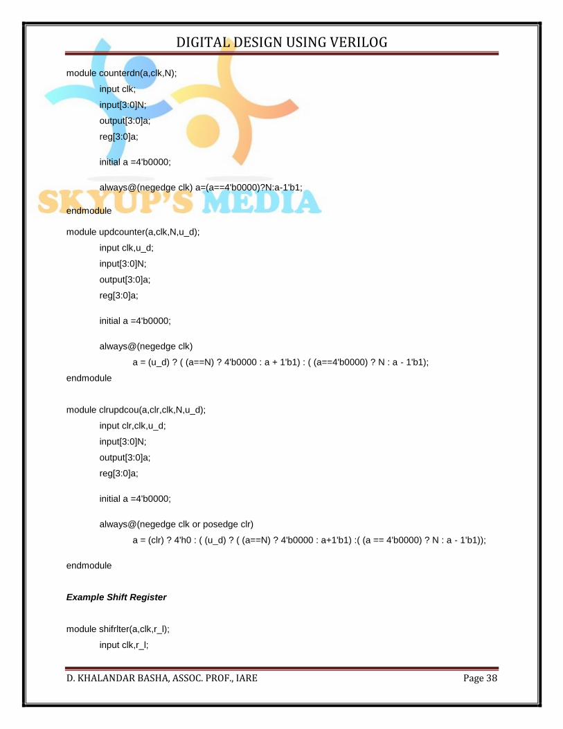
module counterdn(a,clk,N);
input clk;
input[3:0]N;
output[3:0]a;
reg[3:0]a;
initial a =4'b0000;
always@(negedge clk) a=(a==4'b0000)?N:a-1'b1;
endmodule module updcounter(a,clk,N,u_d);
input clk,u_d;
input[3:0]N;
output[3:0]a;
reg[3:0]a;
initial a =4'b0000;
always@(negedge clk)
a = (u_d) ? ( (a==N) ? 4'b0000 : a + 1'b1) : ( (a==4'b0000) ? N : a - 1'b1);
endmodule
module clrupdcou(a,clr,clk,N,u_d);
input clr,clk,u_d;
input[3:0]N;
output[3:0]a;
reg[3:0]a;
initial a =4'b0000;
always@(negedge clk or posedge clr)
a = (clr) ? 4'h0 : ( (u_d) ? ( (a==N) ? 4'b0000 : a+1'b1) :( (a == 4'b0000) ? N : a - 1'b1));
endmodule
Example Shift Register
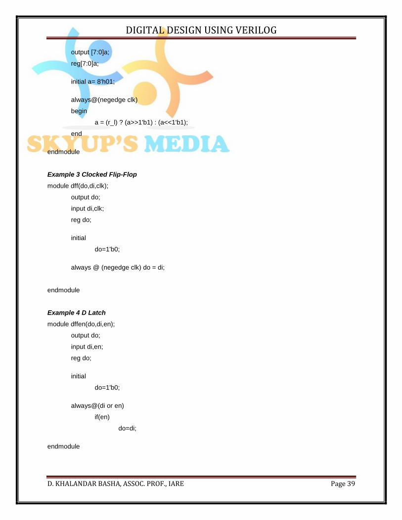
module shifrlter(a,clk,r_l);
input clk,r_l;
DIGITAL DESIGN USING VERILOG
D. KHALANDAR BASHA, ASSOC. PROF., IARE Page 39
output [7:0]a;
reg[7:0]a;
initial a= 8'h01;
always@(negedge clk)
begin
a = (r_l) ? (a>>1'b1) : (a<<1'b1);
end
endmodule
Example 3 Clocked Flip-Flop
module dff(do,di,clk);
output do;
input di,clk;
reg do;
initial
do=1'b0;
always @ (negedge clk) do = di;
endmodule
Example 4 D Latch
module dffen(do,di,en);
output do;
input di,en;
reg do;
initial
do=1'b0;
always@(di or en)
if(en)
do=di;
endmodule

DIGITAL DESIGN USING VERILOG
D. KHALANDAR BASHA, ASSOC. PROF., IARE Page 40
Example 5 Clock Waveform
Consider the design description line
always #3 clk = ~clk;
The sequence of operation taking place within this line segment is as follows:
When the system comes across the statement, it schedules an activity 3 ns later.
At the end of the 3 ns, the value of clk is sensed; the sensed value is complemented and then stored
temporarily.
Then the stored value is assigned to the clock, which completes the activity of the always block; once
again, execution resumes at step 1.
ASSIGNMENTS WITH DELAYS
The delay refers to the specific activity it qualifies. A variety of possibilities of specifying delays
to assignments exist. Consider the assignment
always #3 b = a;
Simulator encounters this at zero time and posts the entire activity to be done 3 ns later the
assignment is scheduled to be repeated every 3 ns, irrespective of whether a changes in the
Meantime
Intra-assignment Delays
In contrast, the “intra-assignment” delay carries out the assignment in two parts
A = # dl expression;
Here the expression is scheduled to be evaluated as soon as it is encountered. However, the result
of the evaluation is assigned to the right-hand side quantity a after a delay specified by dl. dl can
be an integer or a constant expression
Zero Delay
A delay of 0 ns does not really cause any delay. However, it ensures that the assignment
following is executed last in the concerned time slot. Often it is used to avoid indecision in the
precedence of execution of assignments
wait CONSTRUCT
DIGITAL DESIGN USING VERILOG
D. KHALANDAR BASHA, ASSOC. PROF., IARE Page 41
The wait construct makes the simulator wait for the specified expression to be true before
proceeding with the following assignment or group of assignments. Its syntax has the form
wait (alpha) assignment1;
alpha can be a variable, the value on a net, or an expression involving them. If alpha is an
expression, it is evaluated; if true, assignment1 is carried out. One can also have a group of
assignments within a block in place of assignment1. The activity is level-sensitive in nature, in
contrast to the edge-sensitive nature of event specified through @.
Specifically the procedural assignment
@clk a = b;
assigns the value of b to a when clk changes; if the value of b changes when clk is steady, the
value of a remains unaltered.
wait(clk) #2 a = b;
the simulator waits for the clock to be high and then assigns b to a with a delay of 2 ns. The
assignment will be refreshed as long as the clk remains high
DESIGNS AT BEHAVIORAL LEVEL
module aoibeh(o,a,b);
output o;
input[1:0]a,b;
reg o,a1,b1,o1;
always@(a[1] or a[0]or b[1]or b[0])
begin
a1=&a;
b1=&b;
o1=a1||b1;
o=~o1;
end
endmodule
module aoibeh1(o,a,b);
output o;

DIGITAL DESIGN USING VERILOG
D. KHALANDAR BASHA, ASSOC. PROF., IARE Page 42
input[1:0]a,b;
reg o;
always@(a[1]ora[0]or b[1]orb[0])
o=~((&a)||(&b));
endmodule
BLOCKING AND NONBLOCKING ASSIGNMENTS
These are executed sequentially – that is, one statement is executed, and only then the
following one is executed. Such assignments block the execution of the following lot of
assignments at any time step. Hence they are called “blocking assignments”.
A facility called the “nonblocking assignment” is available for such situations. The
symbol “<=” signifies a non-blocking assignment. The same symbol signifies the “less than or
equal to” operator in the context of an operation. The context decides the role of the symbol. The
main characteristic of a nonblocking assignment is that its execution is concurrent with that of
the following assignment or activity.
Nonblocking Assignments and Delays
Delays – of the assignment type and the intra-assignment type – can be associated with
nonblocking assignments also. The principle of their operation is similar to that with blocking
assignments.
THE case STATEMENT
The case statement is an elegant and simple construct for multiple branching in a module. The
keywords case, endcase, and default are associated with thecase construct.
Format of the case construct is
Case (expression)
Ref1 : statement1;
Ref2 : statement2;
Ref3 : statement3;
.. .
. . .
DIGITAL DESIGN USING VERILOG
D. KHALANDAR BASHA, ASSOC. PROF., IARE Page 43
default: statementd;
endcase
If the evaluated value matches ref1, statement1 is executed; and the simulator exits the block;
Else expression is compared with ref2 and in case of a match, statement2 is executed, and so on.
If none of the ref1, ref2, etc., matches the value of expression, the default statement is executed.
A statement or a group of statements is executed if and only if there is an exact – bit by bit –
match between the evaluated expression and the specified ref1, ref2, etc.
For any of the matches, one can have a block of statements defined for execution. The
block should appear within the begin-end construct.
There can be only one default statement or default block. It can appearanywhere in the
case statement.
One can have multiple signal combination values specified for the same statement for
execution. Commas separate all of them.
module dec2_4beh(o,i);
output[3:0]o;
input[1:0]i;
reg[3:0]o;
always@(i)
begin
case(i)
2'b00:o=4'h0;
2'b01:o=4'h1;
2'b10:o=4'h2;
2'b11:o=4'h4;
default:
begin
$display ("error");
o=4'h0;
end
endcase

DIGITAL DESIGN USING VERILOG
D. KHALANDAR BASHA, ASSOC. PROF., IARE Page 44
end
endmodule
module dec2_4beh1(o,i);
output[3:0]o;
input[1:0]i;
reg[3:0]o;
always@(i)
begin
case(i)
2'b00:o[0]=1'b1;
2'b01:o[1]=1'b1;
2'b10:o[2]=1'b1;
2'b11:o[3]=1'b1;
2'b0x,2'b1x,2'bx0,2'bx1:o=4'b0000;
default:
begin
$display ("error");
o=4'h0;
end
endcase
end
endmodule
module alubeh(c,s,a,b,f);
output[3:0]c;
output s;
input [3:0]a,b;
input[1:0]f;
reg s;
reg[3:0]c;
always@(a or b or f)
DIGITAL DESIGN USING VERILOG
D. KHALANDAR BASHA, ASSOC. PROF., IARE Page 45
begin
case(f)
2'b00: c=a+b;
2'b01: c=a-b;
2'b10: c=a&b;
2'b11: c=a|b;
Endcase
end
endmodule
Casex and Casez
The case statement executes a multiway branching where every bit of the case expression
contributes to the branching decision. The statement has two variants where some of the bits of
the case expression can be selectively treated as don’t cares – that is, ignored. Casez allows z to
be treated as a don’t care. “?” character also can be used in place of z. casex treats x or z as a
don’t care
module pri_enc(a,b);
output[1:0]a;
input[3:0]b;
reg[1:0]a;
always@(b)
casez(b)
4'bzzz1:a=2'b00;
4'bzz10:a=2'b01;
4'bz100:a=2'b10;
4'b1000:a=2'b11;
endcase
endmodule
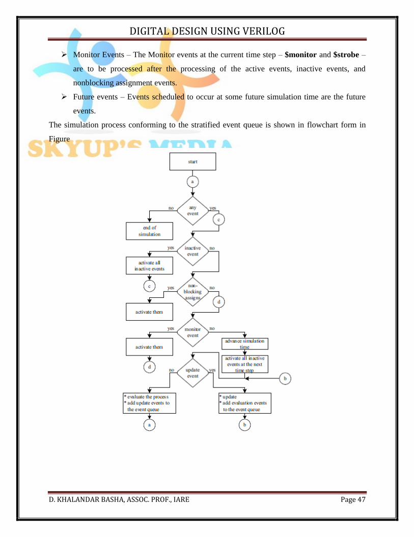
SIMULATION FLOW

DIGITAL DESIGN USING VERILOG
D. KHALANDAR BASHA, ASSOC. PROF., IARE Page 46
Verilog has to be an inherently parallel processing language. The fact that all the elements of a
digital circuit (or any electronic circuit for that matter) function and interact continuously
conforming to their interconnections demands parallel processing. In Verilog theparallel
processing is structured through the following [IEEE]:
Simulation time: Simulation is carried out in simulation time.
The simulator functions with simulation time advancing in (equal) discrete steps.
At every simulation step a number of active events are sequentially carriedout.
The simulator maintains an event queue – called the “Stratified Event Queue” with an
active segment at its top. The top most event in the active segment of the queue is taken
up for execution next.
The active event can be of an update type or evaluation type. The evaluation event can be
for evaluation of variables, values on nets, expressions, etc. Refreshing the queue and
rearranging it constitutes the update event.
Any updating can call for a subsequent evaluation and vice versa.
Only after all the active events in a time step are executed, the simulation advances to the
next time step.
Completion of the sequence of operations above at any time step signifies the parallel nature of
the HDL. A number of active events can be present for execution at any simulation time step; all
may vie for “attention.” Amongst these, an event specified at #0 time is scheduled for execution
at the end
Stratified Event Queue
The events being carried out at any instant give rise to other events – inherent in the execution
process. All such events can be grouped into the following 5 types:
Active events – explained above.
Inactive events – The inactive events are the events lined up for execution immediately
after the execution of the active events. Events specified with zero delay are all inactive
events.
Blocking Assignment Events – Operations and processes carried out at previous time
steps with results to be updated at the current time step are of this category.
DIGITAL DESIGN USING VERILOG
D. KHALANDAR BASHA, ASSOC. PROF., IARE Page 47
Monitor Events – The Monitor events at the current time step – $monitor and $strobe –
are to be processed after the processing of the active events, inactive events, and
nonblocking assignment events.
Future events – Events scheduled to occur at some future simulation time are the future
events.
The simulation process conforming to the stratified event queue is shown in flowchart form in
Figure
DIGITAL DESIGN USING VERILOG
D. KHALANDAR BASHA, ASSOC. PROF., IARE Page 48
if AND if-else CONSTRUCTS
The if construct checks a specific condition and decides execution based on the result. the
structure of a segment of a module with an if statement. After execution of assignment1, the
condition specified is checked. If it is satisfied, assignment2 is executed; if not, it is skipped. In
either case the execution continues through assignment3, assignment4, etc. Execution of
assignment2 alone is dependent on the condition. The rest of the sequence remains.
. . .
assignment1;
if (condition) assignment2;
assignment3;
assignment4;
. . .
Use of the if–else construct
. . .
assignment1;
if(condition)
begin // Alternative 1
assignment2;
assignment3;
end
else
begin //alternative 2
assignment4;
assignment5;
end
assignment6;
. . .
. . .
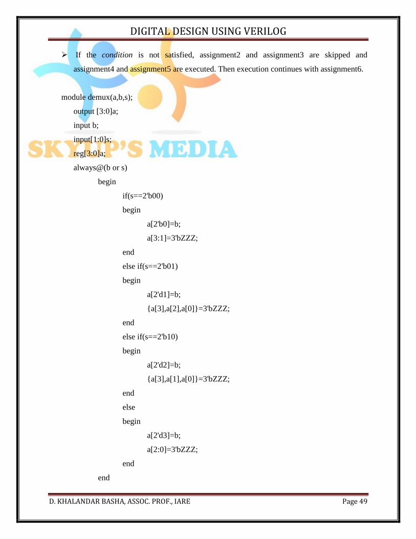
After the execution of assignment1, if the condition is satisfied, alternative1 is followed and
assignment2 and assignment3 are executed. Assignment4 and assignment 5 are skipped and
execution proceeds with assignment6.
DIGITAL DESIGN USING VERILOG
D. KHALANDAR BASHA, ASSOC. PROF., IARE Page 49
If the condition is not satisfied, assignment2 and assignment3 are skipped and
assignment4 and assignment5 are executed. Then execution continues with assignment6.
module demux(a,b,s);
output [3:0]a;
input b;
input[1:0]s;
reg[3:0]a;
always@(b or s)
begin
if(s==2'b00)
begin
a[2'b0]=b;
a[3:1]=3'bZZZ;
end
else if(s==2'b01)
begin
a[2'd1]=b;
{a[3],a[2],a[0]}=3'bZZZ;
end
else if(s==2'b10)
begin
a[2'd2]=b;
{a[3],a[1],a[0]}=3'bZZZ;
end
else
begin
a[2'd3]=b;
a[2:0]=3'bZZZ;
end
end
DIGITAL DESIGN USING VERILOG
D. KHALANDAR BASHA, ASSOC. PROF., IARE Page 50
endmodule
//counter using if else if;
module countif(a,clk);
output[7:0]a;
input clk;
reg[7:0]a,n;
initial
begin
n=8'h0a;
a=8'b00000000;
#45 n=8'h23;
end
always@(posedge clk)
begin
$write ("time=%0d ",$time);
if(a==n)
a=8'h00;
else a=a+1'b1;
end
endmodule
assign–deassign CONSTRUCT
The assign – deassign constructs allow continuous assignments within a behavioral block.
always@(posedge clk) a = b;
By way of execution, at the positive edge of clk the value of b is assigned to variable a, and a
remains frozen at that value until the next positive edge of clk. Changes in b in the interval are
ignored.
Consider the block
always@(posedge clk) assign c = d;

DIGITAL DESIGN USING VERILOG
D. KHALANDAR BASHA, ASSOC. PROF., IARE Page 51
Here at the positive edge of clk, c is assigned the value of d in a continuous manner; subsequent
changes in d are directly reflected as changes in variable c: The assignment here is akin to a
direct (one way ) electrical connection to c from d established at the positive edge of clk.
Consider an enhanced version of the above block as
Always
Begin
@(posedge clk) assign c = d;
@(negedge clk) deassign c;
end
The above block signifies two activities:
1. At the positive edge of clk, c is assigned the value of d in a continuous manner
2. At the following negative edge of clk, the continuous assignment to c is removed; subsequent
changes to d are not passed on to c; it is as though c is electrically disconnected from d.
In short, assign allows a variable or a net change in the sensitivity list to mandate a
subsequent continuous assignment within. deassign terminates the assignment done through the
assign-based statement.
module demux1(a0,a1,a2,a3,b,s);
output a0,a1,a2,a3;
input b;
input [1:0]s;
reg a0,a1,a2,a3;
always@(s)
if(s==2'b00)
assign {a0,a1,a2,a3}={b,3'oz};
else if(s==2'b01)
assign {a0,a1,a2,a3}={1'bz,b,2'bz};
else if(s==2'b10)
assign {a0,a1,a2,a3}={2'bz,b,1'bz};
else if(s==2'b11)

DIGITAL DESIGN USING VERILOG
D. KHALANDAR BASHA, ASSOC. PROF., IARE Page 52
assign {a0,a1,a2,a3}={3'oz,b};
endmodule
D Flip-Flop through assign – deassign Constructs
module dffassign(q,qb,di,clk,clr,pr);
output q,qb;
input di,clk,clr,pr;
reg q;
assign qb=~q;
always@(clr or pr)
begin
if(clr)assign q = 1'b0;//asynchronous clear and
if(pr) assign q = 1'b1;// preset of FF overrides
else deassign q;// the synchronous behaviour
end
always@(posedge clk)
q = di;//synchronous (clocked)value assigned to q
endmodule
repeat CONSTRUCT
The repeat construct is used to repeat a specified block a specified number of times. The
quantity a can be a number or an expression evaluated to a number. As soon as the repeat
statement is encountered, a is evaluated. The following block is executed “a” times. If “a”
evaluates to 0 or x or z, the block is not executed.
Structure of a repeat block.
…
repeat (a)
begin
assignment1;
assignment2;
…
end

DIGITAL DESIGN USING VERILOG
D. KHALANDAR BASHA, ASSOC. PROF., IARE Page 53
…
A module to illustrate the use of the repeat construct
module trial_8b;
reg[7:0] m[15:0];
integer i;
reg clk;
always
begin
repeat(8)
begin
@(negedge clk)
m[i]=i*8;
i=i+1;
end
repeat(8)
begin
@(negedge clk)
i=i-1;
$display("t=%0d, i=%0d, m[i]=%0d", $time,i,m[i]);
end
end
initial
begin
clk = 1'b0;
i=0;
#70 $stop;
end
always #2 clk=~clk;
endmodule

DIGITAL DESIGN USING VERILOG
D. KHALANDAR BASHA, ASSOC. PROF., IARE Page 54
for LOOP
The for loop in Verilog is quite similar to the for loop in C; the format of the for loop is
. . . .
for(assignment1; expression; assignment 2)
statement;
. . .
It has four parts; the sequence of execution is as follows:
1. Execute assignment1.
2. Evaluate expression.
3. If the expression evaluates to the true state (1), carry out statement. Go to step 5.
4. If expression evaluates to the false state (0), exit the loop.
5. Execute assignment2. Go to step 2.
An adder module using the for loop.
module addfor(s,co,a,b,cin,en);
output[7:0]s;
output co;
input[7:0]a,b;
input en,cin;
reg[8:0]c;
reg co;
reg[7:0]s;
integer i;
always@( posedge en )
begin
c[0] =cin;
for(i=0;i<=7;i=i+1)
begin
{c[i+1],s[i]}=(a[i]+b[i]+c[i]);
end
co=c[8];

DIGITAL DESIGN USING VERILOG
D. KHALANDAR BASHA, ASSOC. PROF., IARE Page 55
end
endmodule
THE disable CONSTRUCT
There can be situations where one has to break out of a block or loop. The disable statement
terminates a named block or task. Control is transferred to the statement immediately following
the block. Conditional termination of a loop, interrupt servicing, etc., are typical contexts for its
use. Often the disabling is carried out from within the block itself. The disable construct is
functionally similar to the break in C
OR gate module to demonstrate the use of the disable construct
module or_gate(b,a,en);
input [3:0]a;
input en;
output b;
reg b;
integer i;
always@(posedge en)
begin:OR_gate
b=1'b0;
for(i=0;i<=3;i=i+1)
if(a[i]==1'b1)
begin
b=1'b1;
disable OR_gate;
end
end
endmodule
The disable statement has to have a block (or task) identifier tagged to it in this respect it differs
from “break” in C.
Once encountered, it terminates execution of the block; the following statements within
the block are not executed.
DIGITAL DESIGN USING VERILOG
D. KHALANDAR BASHA, ASSOC. PROF., IARE Page 56
Typically it can be used to handle exceptions to regularly assigned activities for example,
Interrupt, Hold, Reset, etc.
while LOOP
The format for the while loop is shown is
while (expression) statement ;
The Boolean expression is evaluated. If it is true, the statement (or block of statements) is
executed and expression evaluated and checked. If the expression evaluates to false, the loop is
terminated and the following statement is taken for execution. If the expression evaluates to true,
execution of statement (block of statements) is repeated. Thus the loop is terminated and broken
only if the expression evaluates to false.
To generates a pulse of definite width.
module while2(b,n,en,clk);
input[7:0]n;
input clk,en;
output b;
reg[7:0]a;
reg b;
always@(posedge en)
begin
a=n;
while(|a)
begin
b=1'b1;
@(posedge clk)
a=a-1'b1;
end
b=1'b0;
end
initial b=1'b0;
endmodule

DIGITAL DESIGN USING VERILOG
D. KHALANDAR BASHA, ASSOC. PROF., IARE Page 57
forever LOOP
Repeated execution of a block in an endless manner is best done with the forever loop (compare
with repeat where the repetition is for a fixed number of times).
module to generate a clock waveform using the forever construct
module clk;
reg clk, en;
always @(posedge en)
forever#2 clk=~clk;
initial
begin
clk=1'b0; en=1'b0;#1 clk=1'b1; #4 en=1'b1;#30 $stop;
end
initial $monitor("clk=%b, t=%0d, en=%b ", clk,$time,en);
endmodule
PARALLEL BLOCKS
All the procedural assignments within a begin–end block are executed sequentially. The
fork–join block is an alternate one where all the assignments are carried out concurrently. One
can use a fork-join block within a begin–end block or vice versa.
module fk_jn_a;
integer a;
initial
begin
a=0;
#1 a=1;
#2 a=2;
#3 a=3;
#4 $stop;
end
initial $monitor ("a=%0d,
module fk_jn_b;
integer a;
initial
fork
a=0;
#1 a=1;
#2 a=2;
#3 a=3;
#4 $stop;
join
initial $monitor ("a=%0d,

DIGITAL DESIGN USING VERILOG
D. KHALANDAR BASHA, ASSOC. PROF., IARE Page 58
t=%0d",a,$time);
endmodule
//Simulatiom results
# a=0, t=0
# a=1, t=1
# a=2, t=3
# a=3, t=6
t=%0d",a,$time);
endmodule
//Simulation results
# a=0, t=0
# a=1, t=1
# a=2, t=2
# a=3, t=3
Force–release CONSTRUCT
When debugging a design with a number of instantiations, one may be stuck with an unexpected
behavior in a localized area. Tracing the paths of individual signals and debugging the design
may prove to be too tedious or difficult. In such cases suspect blocks may be isolated, tested, and
debugged and status quo ante established. The force–release construct is for such a localized
isolation for a limited period.
force a = 1'b0;
forces the variable a to take the value 0.
force b = c&d;
forces the variable b to the value obtained by evaluating the expression c&d.
The force–release construct is similar to the assign–deassign construct. The latter construct is
for conditional assignment in a design description. The force–release construct is for “short
time” assignments in a test-bench. Synthesis tools will not support the force–release
constructs.
The force–release construct is equally valid for net-type variables and reg-type variables.
The net–type variables revert to their normal values on release. With reg-type variables
the value forced remains until another assignment to the reg.
The variable, on which the values are forced during testing, must be properly
dereferenced.
In the illustration above, each variable was forced one at a time. It was done only to
simplify the illustration sequence and focus attention on the possible use of the construct.
In practice, different variables can be forced together before the special debug sequence.
Their release too can be together.

DIGITAL DESIGN USING VERILOG
D. KHALANDAR BASHA, ASSOC. PROF., IARE Page 59
OR gate module and its test bench to illustrate the use of force–release construct
module or_fr_rl(a,b,c);
input b,c; output a; wire a,b,c;
assign a= b|c;
initial
begin
#1 $display("display:time=%0d, b=%b, c=%b, a=%b", $time,b,c,a);
#6 force b=1'b1;
#1 $display("display:time=%0d, b=%b, c=%b, a=%b", $time,b,c,a);
#6 release b;
#1 $display("display:time=%0d, b=%b, c=%b, a=%b", $time,b,c,a);
end
endmodule
EVENT
The keyword event allows an abstract event to be declared. The event is not a data type
with any specific values; it is not a variable (reg) or a net. It signifies a change that can be used
as a trigger to communicate between modules or to synchronize events in different modules.
. . .
event change;
. . .
always
. . .
. . . change;
. . .
.always@change
. . .
In the course of execution of an always block, the event is triggered. The operator “”
signifies the triggering. Subsequently, another activity can be started in the module by the event
change. The always@(change) block activates this. The event change can be used in other

DIGITAL DESIGN USING VERILOG
D. KHALANDAR BASHA, ASSOC. PROF., IARE Page 60
modules also by proper dereferencing; with such usage an activity in a module can be
synchronized to an event in another module.
The event construct is quite useful, especially in the early stages of a design. It can be used to
establish the functionality of a design at the behavioral level; it allows communication amongst
different instantiated modules without associated inputs or outputs.
A module to illustrate the event construct: A serial data receiver
module rec(a,ddi,clk);
output[8:1]a; input ddi,clk;reg[8:1] a;integer j,jj;
event buf_ful;
always for (j=0;j<20;j=j+1)
begin
#0 jj=0;
repeat(8)@(negedge clk)
begin
jj=jj+1;
a[jj]=ddi;
//$display("b=%b",a[jj]);
end
#0 ->buf_ful;
end
endmodule
DIGITAL DESIGN USING VERILOG
D. KHALANDAR BASHA, ASSOC. PROF., IARE Page 61
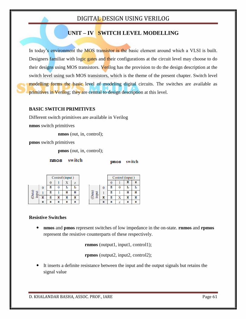
UNIT – IV SWITCH LEVEL MODELLING
In today’s environment the MOS transistor is the basic element around which a VLSI is built.
Designers familiar with logic gates and their configurations at the circuit level may choose to do
their designs using MOS transistors. Verilog has the provision to do the design description at the
switch level using such MOS transistors, which is the theme of the present chapter. Switch level
modelling forms the basic level of modeling digital circuits. The switches are available as
primitives in Verilog; they are central to design description at this level.
BASIC SWITCH PRIMITIVES
Different switch primitives are available in Verilog
nmos switch primitives
nmos (out, in, control);
pmos switch primitives
pmos (out, in, control);
Resistive Switches
nmos and pmos represent switches of low impedance in the on-state. rnmos and rpmos
represent the resistive counterparts of these respectively.
rnmos (output1, input1, control1);
rpmos (output2, input2, control2);
It inserts a definite resistance between the input and the output signals but retains the
signal value

DIGITAL DESIGN USING VERILOG
D. KHALANDAR BASHA, ASSOC. PROF., IARE Page 62
The rpmos and rnmos switches function as unidirectional switches; the signal flow is
from the input to the output side.
strength levels
Output-side strength levels for different input-side strength values of rnmos, rpmos, and
rcmos switches
pullup and pulldown
A MOS transistor functions as a resistive element when in the active state. Realization of
resistance in this form takes less silicon area in the IC as compared to a resistance
realized directly. pullup and pulldown represent such resistive elements.
pullup (x);
Here net x is pulled up to the supply1 through a resistance.
pulldown(y);
pulls y down to the supply0 level through a resistance.
The pullup and pulldown primitives can be used as loads for switches or to connect the unused
input ports to VCC or GND, respectively.
CMOS SWITCH
A CMOS switch is formed by connecting a PMOS and an NMOS switch in parallel – the
input leads are connected together on the one side and the output leads are connected
together on the other side.
The CMOS switch is instantiated as shown below.
cmos csw (out, in, N_control, P_control );
BI-DIRECTIONAL GATES
Verilog has a set of primitives for bi-directional switches as well. They connect the nets
on either side when ON and isolate them when OFF. The signal flow can be in either
direction
tran and rtran
The tran gate is a bi-directional gate of two ports. When instantiated, it connects the
two ports directly.
tran (s1, s2);

DIGITAL DESIGN USING VERILOG
D. KHALANDAR BASHA, ASSOC. PROF., IARE Page 63
connects the signal lines s1 and s2.
Either line can be input, inout or output.
rtran is the resistive counterpart of tran.
tranif1 and rtranif1
tranif1 is a bi-directional switch turned ON/OFF through a control line(c). It is in the
ON-state when the control signal is at 1 (high) state
tranif1 (s1, s2, c );
tranif0 and rtranif0
tranif0 and rtranif0 are again bi-directional switches. The switch is OFF if the control
line is in the 1 state, and it is ON when the control line is in the 0 state.
tranif0 (s1, s2, c);
TIME DELAYS WITH SWITCH PRIMITIVES
nmos g1 (out, in, ctrl );
has no delay associated with it. The instantiation
nmos (delay1) g2 (out, in, ctrl );
has delay1 as the delay for the output to rise, fall, and turn OFF.
nmos (delay_r, delay_f) g3 (out, in, ctrl );
has delay_r as the rise-time for the output. delay_f is the fall-time for the output. The
turn-off time is zero.
nmos (delay_r, delay_f, delay_o) g4 (out, in, ctrl );
has delay_r as the rise-time for the output. delay_f is the fall-time for the output delay_o
is the time to turn OFF when the control signal ctrl goes from 0 to 1.
Delays can be assigned to the other uni-directional gates in a similar manner.
Bi-directional switches do not delay transmission – their rise- and fall-times are zero.
They can have only turn-on and turn-off delays associated with them.
tran has no delay associated with it.

DIGITAL DESIGN USING VERILOG
D. KHALANDAR BASHA, ASSOC. PROF., IARE Page 64
tranif1 (delay_r, delay_f) g5 (out, in, ctrl );
When control changes from 0 to 1, the switch turns on with a delay of delay_r. When control
changes from 1 to 0, the switch turns off with a delay of delay_f.
transif1 (delay0) g2 (out, in, ctrl );
represents an instantiation with delay0 as the delay for the switch to turn on when control
changes from 0 to 1, with the same delay for it to turn off when control changes from 1 to 0
INSTANTIATIONS WITH STRENGTHS AND DELAYS
nmos (strong1, strong0) (delay_r, delay_f, delay_o ) gg (s1, s2, ctrl) ;
rnmos, pmos, and rpmos switches too can be instantiated in the general form in
the same manner. The general instantiation for the bi-directional gates too can be
done similarly.
STRENGTH CONTENTION WITH TRIREG NETS
nets declared as trireg can have capacitive storage. Such storage can be assigned one of
three strengths – large, medium, or small.
Driving such a net from different sources can lead to contention
PARAMETERS
Constants signifying timing values, ranges of variables, wires, etc., can be specified in
terms of assigned names. Such assigned names are called parameters.
Two types of parameters are of use in modules
Parameters related to timings, time delays, rise and fall times, etc., are
technology-specific and used during simulation. Parameter values can be assigned
or overridden with the keyword “specparam” preceding the assignments.
Parameters related to design, bus width, and register size are of a different
category. They are related to the size or dimension of a specific design; they are
technology-independent. Assignment or overriding is with assignments following
the keyword “defparam”.
PATH DELAYS

DIGITAL DESIGN USING VERILOG
D. KHALANDAR BASHA, ASSOC. PROF., IARE Page 65
Verilog has the provision to specify and check delays associated with total paths – from
any input to any output of a module. Such paths and delays are at the chip or system
level. They are referred to as “module path delays.”
Specify Blocks
Module paths are specified and values assigned to their delays through specify
blocks. They are used to specify rise time, fall time, path delays pulse widths.
specify
specparam rise_time = 5, fall_time = 6;
(a =>b) = (rise_time, fall_time);
(c => d) = (6, 7);
endspecify
Module Paths
Module paths can be specified in different ways inside a specify block. The simplest has the form
A*>B
Here “A” is the source and “B” the destination.
specify
(a,b*>s)=1;
(a,b*>ca)=2;
endspecify
Conditional Pin-to-Pin Delays
The pin to pin path of a signal may change depending on the value of another signal; in turn the
number of circuit elements in the alternate path may differ.
specify
if(f==2'b00)(a=>d)=1;
if(f >2'b00)(a=>d)=2;
(b,cci*>co)=1;
endspecify
DIGITAL DESIGN USING VERILOG
D. KHALANDAR BASHA, ASSOC. PROF., IARE Page 66
MODULE PARAMETERS
Module parameters are associated with size of bus, register, memory, ALU, and so on. They can
be specified within the concerned module but their value can be altered during instantiation. The
alterations can be brought about through assignments made with defparam. Such defparam
assignments can appear anywhere in a module.
SYSTEM TASKSANDFUNCTIONS
A “$” sign preceding a word or a word group signifies a system task or a system function
Output Tasks
$monitor and $display
Display Tasks
The $display task, whenever encountered, displays the arguments in the desired format; and the
display advances to a new line. $write task carries out the desired display but does not advance to the new
line
$strobe Task
When a variable or a set of variables is sampled and its value displayed, the $strobe task can be
used; it senses the value of the specified variables and displays them.
$monitor Task
$monitor task is activated and displays the arguments specified whenever any of the arguments
changes
$stop and $finish Tasks
The $stop task suspends simulation.
$finish stops simulation, closes the simulation environment, and
reverts to the operating system.
$random Function
One can start with a seed number (optional) and generate a random number repeatedly. Such
random number sequences can be fruitfully used for testing.
FILE-BASED TASKS AND FUNCTIONS
DIGITAL DESIGN USING VERILOG
D. KHALANDAR BASHA, ASSOC. PROF., IARE Page 67
To carry out any file-based task, the file has to be opened, reading, writing, etc., completed and
the file closed. The keywords for all file-based tasks start with the letter f to distinguish them
from the other tasks
All the system tasks to output information can be used to output to a file.
$display, $strobe, $monitor, etc., are of this category. The respective
keywords to output to the file are $fdisplay, $fstrobe, $fmonitor.
The first field of the task statement is an argument – the file descriptor. The subsequent fields are
identical to the corresponding nonfile tasks.
COMPILER DIRECTIVES
They allow for macros, inclusion of files, and timescale-related parameters for simulation. All
compiler directives are preceded by the ‘`’.
`define Directive
The `define directive is used to define and associate the desired text with the macro name
`define add 2'b00
Time-Related Tasks
The `timescale compiler directive allows the time scale to be specified for the design. The
`timescale directive has two components
`timescale 1 ms/100 μs
HIERARCHICAL ACCESS
A Verilog design will normally have a module or two at the apex level. A number of modules and
UDPs will be instantiated within it.
$display("fad.a = %0d, fad.b = %0d, fad.fad = %0d", fad.a,fad.b,fad.fad);
USER-DEFINED PRIMITIVES (UDP)
The primitives available in Verilog are all of the gate or switch types. Verilog has the provision
for the user to define primitives – called “user defined primitive (UDP)” and use them.
A UDP can be defined anywhere in a source text and instantiated in any of the modules. Their
definition is in the form of a table in a specific format.
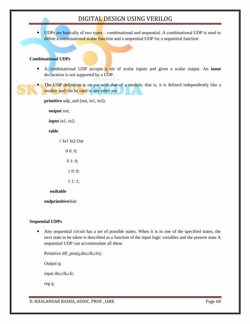
DIGITAL DESIGN USING VERILOG
D. KHALANDAR BASHA, ASSOC. PROF., IARE Page 68
UDPs are basically of two types – combinational and sequential. A combinational UDP is used to
define a combinational scalar function and a sequential UDP for a sequential function
Combinational UDPs
A combinational UDP accepts a set of scalar inputs and gives a scalar output. An inout
declaration is not supported by a UDP.
The UDP definition is on par with that of a module; that is, it is defined independently like a
module and can be used in any other mo
primitive udp_and (out, in1, in2);
output out;
input in1, in2;
table
// In1 In2 Out
0 0: 0;
0 1: 0;
1 0: 0;
1 1: 1;
endtable
endprimitivedule
Sequential UDPs
Any sequential circuit has a set of possible states. When it is in one of the specified states, the
next state to be taken is described as a function of the input logic variables and the present state A
sequential UDP can accommodate all these.
Primitive dff_pos(q,din,clk,clr);
Output q;
input din,clk,clr;
reg q;

DIGITAL DESIGN USING VERILOG
D. KHALANDAR BASHA, ASSOC. PROF., IARE Page 69
table
// din clk clr qp qn Whatever be the present
0 (01) 0: ?: 0; // state of the output, at the
1 (01) 0: ?: 1; // positive edge of clk input
? (10) 0: ?: -; // value is latched and
end table
end primitive
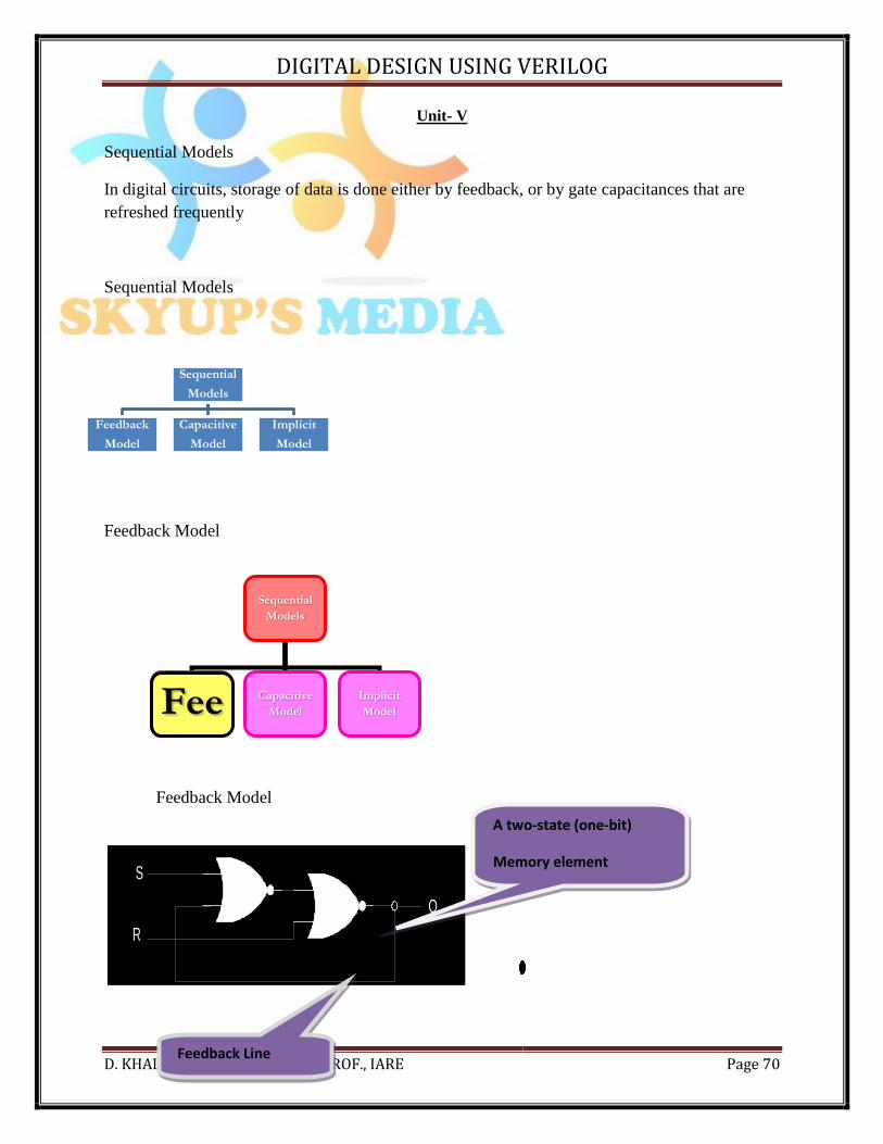
DIGITAL DESIGN USING VERILOG
D. KHALANDAR BASHA, ASSOC. PROF., IARE Page 70
Unit- V
Sequential Models
In digital circuits, storage of data is done either by feedback, or by gate capacitances that are
refreshed frequently
Sequential Models
Feedback Model
Feedback Model
Sequential
Models
Feedback
Model
Capacitive
Model
Implicit
Model
Sequential
Models
Feedback
Model
Capacitive
Model
Implicit
Model Fee
dba
S
R
Q
S
R
Q
A two-state (one-bit)
Memory element
Feedback Line
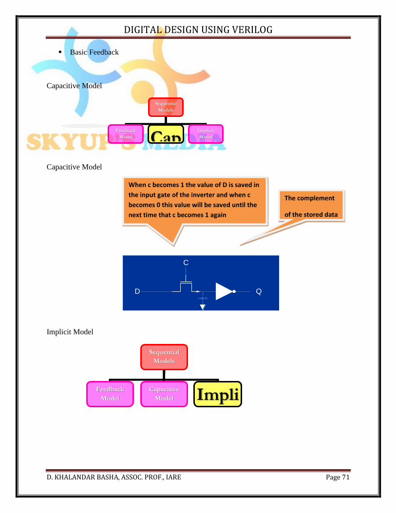
DIGITAL DESIGN USING VERILOG
D. KHALANDAR BASHA, ASSOC. PROF., IARE Page 71
Basic Feedback
Capacitive Model
Capacitive Model
Implicit Model
Sequential
Models
Feedback
Model
Capacitive
Model
Implicit
Model Cap
D
C
Q
When c becomes 1 the value of D is saved in
the input gate of the inverter and when c
becomes 0 this value will be saved until the
next time that c becomes 1 again
The complement
of the stored data
Sequential
Models
Feedback
Model
Capacitive
Model
Implicit
Model Impli
cit
DIGITAL DESIGN USING VERILOG
D. KHALANDAR BASHA, ASSOC. PROF., IARE Page 72
Implicit Model
Basic Memory Components
Gate Level Primitives
1S
1R
Q
C1
Basic Memory
Components
Gate Level Primitives
User Defined
Sequential Primitives
Memory Elements
Using Assignments
Behavioral
Memory Elements
Flip-flop Timing Memory Vectors
and Arrays
Basic Memory
Components
Gate Level Primitives
User Defined
Sequential Primitives
Memory Elements
Using Assignments
Behavioral
Memory Elements
Flip-flop Timing Memory Vectors
and Arrays
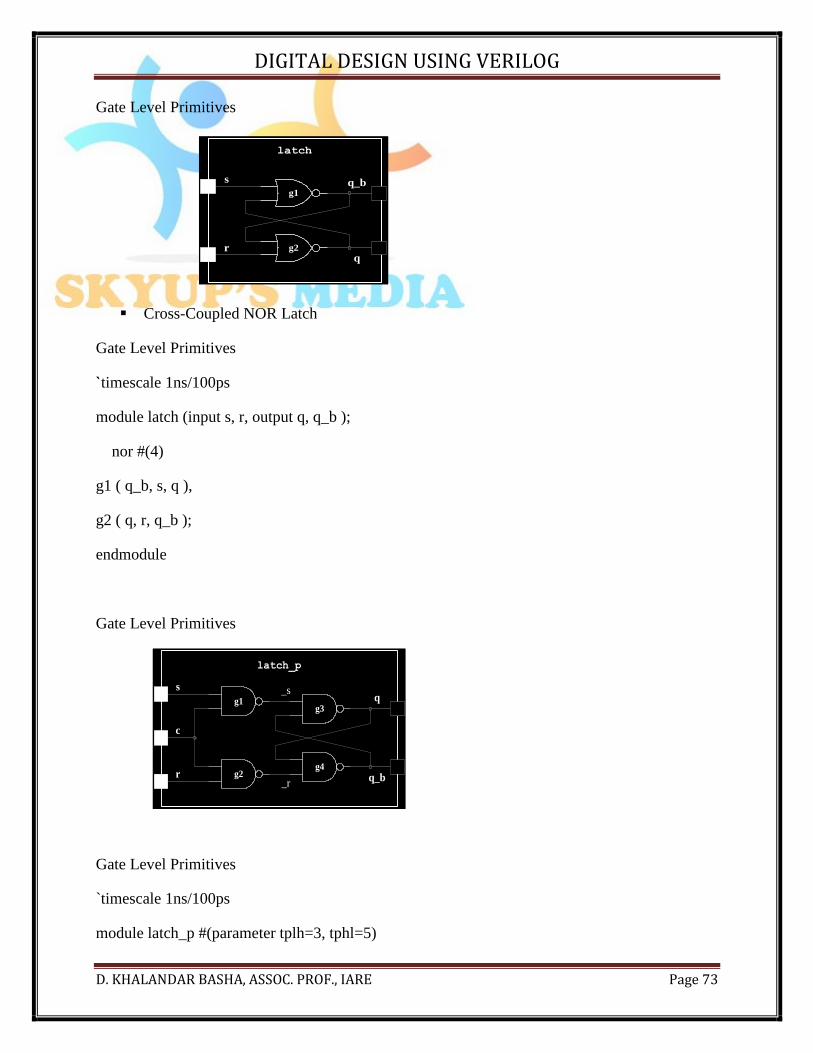
DIGITAL DESIGN USING VERILOG
D. KHALANDAR BASHA, ASSOC. PROF., IARE Page 73
Gate Level Primitives
Cross-Coupled NOR Latch
Gate Level Primitives
`timescale 1ns/100ps
module latch (input s, r, output q, q_b );
nor #(4)
g1 ( q_b, s, q ),
g2 ( q, r, q_b );
endmodule
Gate Level Primitives
Gate Level Primitives
`timescale 1ns/100ps
module latch_p #(parameter tplh=3, tphl=5)
s
rq
g1
g2
q_b
latch
_s
_rq_b
g1
g2
q
latch_p
s
c
rg4
g3

DIGITAL DESIGN USING VERILOG
D. KHALANDAR BASHA, ASSOC. PROF., IARE Page 74
(input s, r, c, output q, q_b );
wire _s, _r;
nand #(tplh,tphl)
g1 ( _s, s, c ),
g2 ( _r, r, c ),
g3 ( q, _s, q_b ),
g4 ( q_b, _r, q );
endmodule
Gate Level Primitives
SR Latch Simulation
Gate Level Primitives
latch
d
c~c
qm
qm_b~d
master_slave
q
q_b
latch

DIGITAL DESIGN USING VERILOG
D. KHALANDAR BASHA, ASSOC. PROF., IARE Page 75
Master-Slave D Flip-Flop
Gate Level Primitives
`timescale 1ns/100ps
module master_slave (input d, c, output q, q_b );
wire qm, qm_b;
defparam master.tplh=4, master.tphl=4,
slave.tplh=4, slave.tphl=4;
latch_p
master ( d, ~d, c, qm, qm_b ),
slave ( qm, qm_b, ~c, q, q_b );
endmodule
Master-Slave D Flip-Flop Verilog Code
User Defined Sequential Primitives
User Defined Sequential Primitives
Verilog provides language constructs for defining sequential UDPs:
Faster Simulation of memory elements
Basic
Memory
ComponenGate Level
Primitives User
Defined Sequential
Memory
Elements Using
Behavioral Memory
Elements Flip-flop
Timing Memory
Vectors and Arrays
User
Defi

DIGITAL DESIGN USING VERILOG
D. KHALANDAR BASHA, ASSOC. PROF., IARE Page 76
Correspondence to specific component libraries
User Defined Sequential Primitives
primitive latch( q, s, r, c );
output q;
reg q;
input s, r, c;
initial q=1'b0;
table
// s r c q q+ ;
// ------:---:----;
? ? 0 : ? : - ;
0 0 1 : ? : - ;
0 1 1 : ? : 0 ;
1 0 1 : ? : 1 ;
endtable
endprimitive
Sequential UDP Defining a Latch
User Defined Sequential Primitives
primitive latch( q, s, r, c );
.............
.............
table

DIGITAL DESIGN USING VERILOG
D. KHALANDAR BASHA, ASSOC. PROF., IARE Page 77
// s r c q q+ ;
// ------:---:----;
? ? 0 : ? : - ;
0 0 1 : ? : - ;
0 1 1 : ? : 0 ;
1 0 1 : ? : 1 ;
endtable
endprimitive
Memory Elements Using Assignments
Memory Elements Using Assignments
Basic Memory
Components
Gate Level Primitives
User Defined
Sequential Primitives
Memory Elements
Using Assignments
Behavioral
Memory Elements
Flip-flop Timing Memory Vectors
and Arrays
d
c
qm
master_slave
q
~c

DIGITAL DESIGN USING VERILOG
D. KHALANDAR BASHA, ASSOC. PROF., IARE Page 78
Master-Slave Using Two Feedback Blocks
Memory Elements Using Assignments
`timescale 1ns/100ps
module master_slave_p #(parameter delay=3)
(input d, c, output q);
wire qm;
assign #(delay) qm = c ? d : qm;
assign #(delay) q = ~c ? qm : q;
endmodule
Assign Statements Implementing Logic Feedback
Behavioral Memory Elements
Behavioral Memory Elements
Basic Memory
Components
Gate Level Primitives
User Defined
Sequential Primitives
Memory Elements
Using Assignments
Behavioral
Memory Elements
Flip-flop Timing Memory Vectors
and Arrays
DIGITAL DESIGN USING VERILOG
D. KHALANDAR BASHA, ASSOC. PROF., IARE Page 79
Behavioral Coding:
A more abstract and easier way of writing Verilog code for a latch or
flip-flop.
The storage of data and its sensitivity to its clock and other control inputs will be
implied in the way model is written.
Behavioral Memory Elements
Latch Modeling
Latch Modeling
timescale 1ns/100ps
module latch (input d, c, output reg q, q_b );
always @( c or d )
if ( c )
begin
Behavioral
Memory
Elements
Latch
Modeling
Flip-flop
Modeling
Flip-flop
with Set-Reset
Control
Other
Storage Element
Modeling Styles
Behavioral
Memory
Elements
Latch Modeling Flip-flop
Modeling
Flip-flop
with Set-Reset
Control
Other
Storage Element
Modeling Styles
Latch

DIGITAL DESIGN USING VERILOG
D. KHALANDAR BASHA, ASSOC. PROF., IARE Page 80
#4 q = d;
#3 q_b = ~d;
end
endmodule
A D-Type Latch Verilog Code
Latch Modeling
`timescale 1ns/100ps
module latch (input d, c, output reg q, q_b );
always @( c or d )
if ( c )
begin
q <= #4 d;
q_b <= #3 ~d;
end
endmodule
Latch Model Using Nonblocking Assignments
Latch Modeling
Testing Latch with Nonblocking Assignments
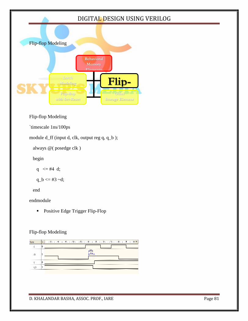
DIGITAL DESIGN USING VERILOG
D. KHALANDAR BASHA, ASSOC. PROF., IARE Page 81
Flip-flop Modeling
Flip-flop Modeling
`timescale 1ns/100ps
module d_ff (input d, clk, output reg q, q_b );
always @( posedge clk )
begin
q <= #4 d;
q_b <= #3 ~d;
end
endmodule
Positive Edge Trigger Flip-Flop
Flip-flop Modeling
Behavioral
Memory
Elements
Latch Modeling
Flip-flop Modeling
Flip-flop with Set-Reset
Control Other
Storage Element
Modeling Styles
Flip-
flop

DIGITAL DESIGN USING VERILOG
D. KHALANDAR BASHA, ASSOC. PROF., IARE Page 82
Simulation of a Positive Edge Flip-Flop
Flip-flop with Set-Reset Control
Flip-flop With Set-Reset Control
`timescale 1ns/100ps
module d_ff_sr_Synch (input d, s, r, clk, output reg q, q_b );
always @(posedge clk) begin
if( s ) begin
q <= #4 1'b1;
q_b <= #3 1'b0;
end else if( r ) begin
q <= #4 1'b0;
q_b <= #3 1'b1;
end else begin
q <= #4 d;
q_b <= #3 ~d;
end
end
Behavioral
Memory
Elements
Latch Modeling Flip-flop
Modeling Flip-flop
with Set-Reset Control
Other Storage Element Modeling Styles Flip-
flop

DIGITAL DESIGN USING VERILOG
D. KHALANDAR BASHA, ASSOC. PROF., IARE Page 83
endmodule
D Type Flip-Flop with Synchronous Control
Flip-flop With Set-Reset Control
module d_ff_sr_Synch (input d, s, r, clk,
output reg q, q_b );
always @(posedge clk) begin
if( s ) begin
.................
end else if( r ) begin
.................
end else begin
.................
end
end
endmodule
D Type Flip-Flop with Synchronous Control (Continued)
Flip-flop With Set-Reset Control
..................
if( s ) begin
q <= #4 1'b1;
q_b <= #3 1'b0;
end else if( r ) begin

DIGITAL DESIGN USING VERILOG
D. KHALANDAR BASHA, ASSOC. PROF., IARE Page 84
q <= #4 1'b0;
q_b <= #3 1'b1;
end else begin
q <= #4 d;
q_b <= #3 ~d;
end
timescale 1ns/100ps
module d_ff_sr_Asynch (input d, s, r, clk, output reg q, q_b );
always @( posedge clk, posedge s, posedge r )
begin
if( s ) begin
q <= #4 1'b1;
q_b <= #3 1'b0;
end else if( r ) begin
q <= #4 1'b0;
q_b <= #3 1'b1;
end else begin
q <= #4 d;
q_b <= #3 ~d;
end
end
endmodule
D-type Flip-Flop with Asynchronous Control

DIGITAL DESIGN USING VERILOG
D. KHALANDAR BASHA, ASSOC. PROF., IARE Page 85
Flip-flop With Set-Reset Control
module d_ff_sr_Asynch (input d, s, r, clk,
output reg q, q_b );
always @( posedge clk, posedge s, posedge r ) begin
if( s ) begin
....................
end else if( r ) begin
....................
end else begin
....................
end
end
endmodule
....................
if( s ) begin
q <= #4 1'b1;
q_b <= #3 1'b0;
end else if( r ) begin
q <= #4 1'b0;
q_b <= #3 1'b1;
end else begin
q <= #4 d;
q_b <= #3 ~d;
end
....................

DIGITAL DESIGN USING VERILOG
D. KHALANDAR BASHA, ASSOC. PROF., IARE Page 86
D-type Flip-Flop with Asynchronous Control
Flip-flop With Set-Reset Control
Other Storage Element Modeling Styles
Other Storage Element Modeling Styles
`timescale 1ns/100ps
module latch (input d, c, output reg q, q_b );
always begin
wait ( c );
#4 q <= d;
#3 q_b <= ~d;
Behavioral
Memory
Elements
Latch Modeling Flip-flop
Modeling Flip-flop
with Set-Reset Control
Other Storage Element Modeling
Style Oth
er
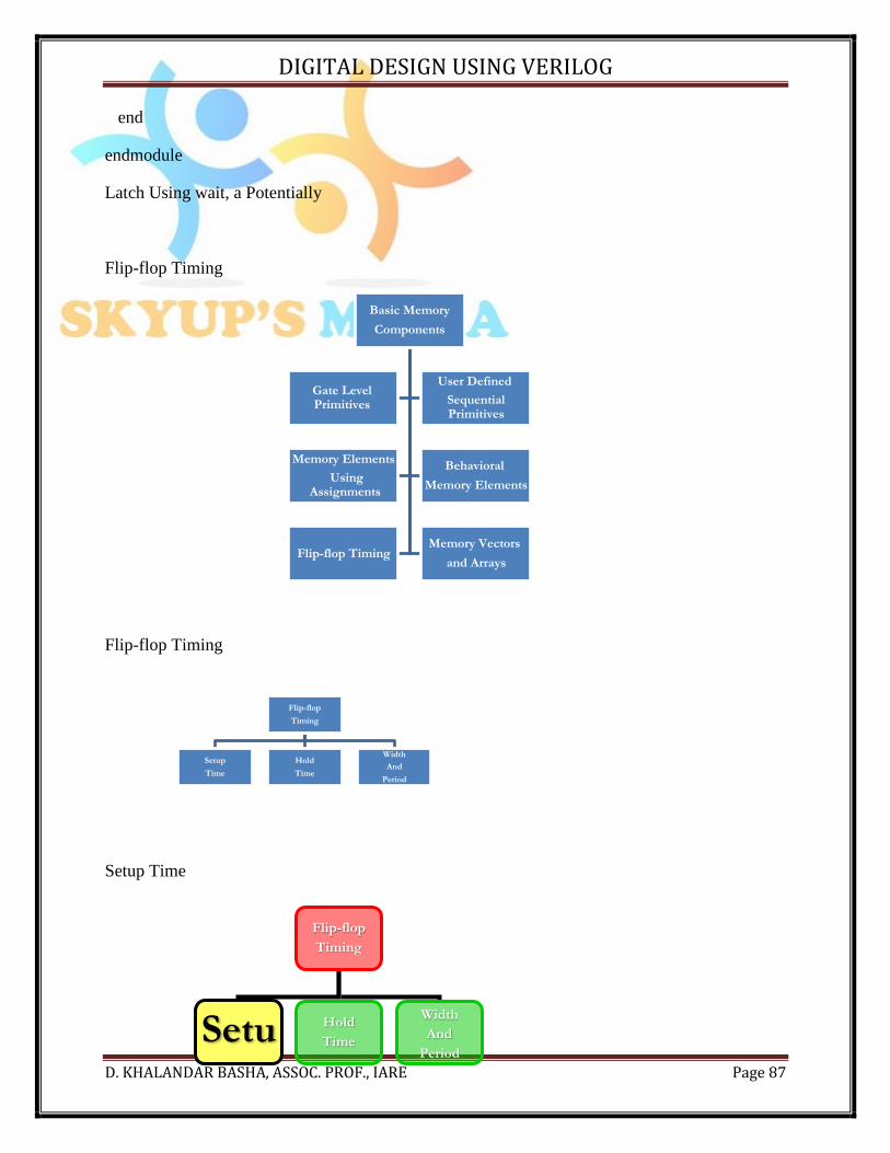
DIGITAL DESIGN USING VERILOG
D. KHALANDAR BASHA, ASSOC. PROF., IARE Page 87
end
endmodule
Latch Using wait, a Potentially
Flip-flop Timing
Flip-flop Timing
Setup Time
Basic Memory
Components
Gate Level Primitives
User Defined
Sequential Primitives
Memory Elements
Using Assignments
Behavioral
Memory Elements
Flip-flop Timing Memory Vectors
and Arrays
Flip-flop
Timing
Setup
Time
Hold
Time
Width
And
Period
Flip-flop
Timing
Setup
Time
Hold
Time
Width
And
Period Setu
p

DIGITAL DESIGN USING VERILOG
D. KHALANDAR BASHA, ASSOC. PROF., IARE Page 88
Setup Time
Setup Time
The Minimum necessary time that a data input requires to setup before it is
clocked into a flip-flop.
Verilog construct for checking the setup time: $setup task
The $setup task:
Takes flip-flop data input, active clock edge and the setup time as its parameters.
Is used within a specify block
`timescale 1ns/100ps
module d_ff ( input d, clk, s, r, output reg q, q_b );
specify
$setup ( d, posedge clk, 5 );
endspecify
always @( posedge clk or posedge s or posedge r )
begin
..............
end
endmodule
...................................
always @( posedge clk or posedge s or posedge r )
begin
if( s ) begin
q <= #4 1'b1;
q_b <= #3 1'b0;
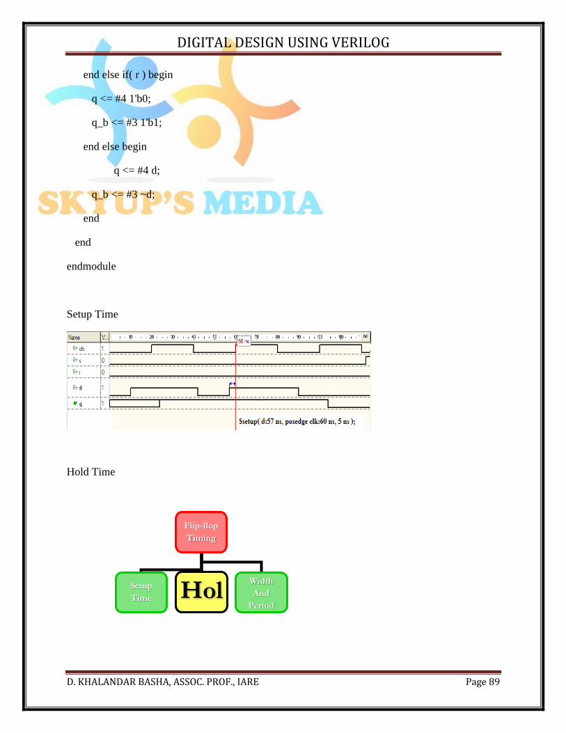
DIGITAL DESIGN USING VERILOG
D. KHALANDAR BASHA, ASSOC. PROF., IARE Page 89
end else if( r ) begin
q <= #4 1'b0;
q_b <= #3 1'b1;
end else begin
q <= #4 d;
q_b <= #3 ~d;
end
end
endmodule
Setup Time
Hold Time
Flip-flop
Timing
Setup
Time
Hold
Time
Width
And
Period Hol
d

DIGITAL DESIGN USING VERILOG
D. KHALANDAR BASHA, ASSOC. PROF., IARE Page 90
Hold Time
Hold Time
The Minimum necessary time a flip-flop data input must stay stable (holds its
value) after it is clocked.
Verilog construct for checking the setup time: $hold task
The $setup task:
Takes flip-flop data input, active clock edge and the required hold time as its
parameters.
Is used within a specify block.
`timescale 1ns/100ps
module d_ff ( input d, clk, s, r, output reg q, q_b);
specify
$hold ( posedge clk, d, 3 );
endspecify
always @( posedge clk or posedge s or posedge r )
begin
..............................................
end
endmodule
Flip-Flop with Hold Time

DIGITAL DESIGN USING VERILOG
D. KHALANDAR BASHA, ASSOC. PROF., IARE Page 91
Hold Time
Hold Time Violation
Hold Time
The Verilog $setuphold task combines setup and hold timing checks.
Example:
$setuphold (posedge clk, d, 5, 3)
Width And Period
Width And Period
Verilog $width and $period check for minimum pulse width and period.
Pulse Width: Checks the time from a specified edge of a reference signal to its opposite
edge.
Period: Checks the time from a specified edge of a reference signal to the same edge.
Flip-flop
Timing
Setup
Time
Hold
Time
Width
And
Period
Widt
h
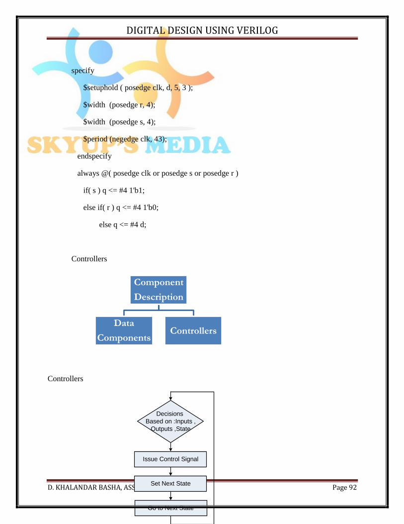
DIGITAL DESIGN USING VERILOG
D. KHALANDAR BASHA, ASSOC. PROF., IARE Page 92
specify
$setuphold ( posedge clk, d, 5, 3 );
$width (posedge r, 4);
$width (posedge s, 4);
$period (negedge clk, 43);
endspecify
always @( posedge clk or posedge s or posedge r )
if( s ) q <= #4 1'b1;
else if( r ) q <= #4 1'b0;
else q <= #4 d;
Controllers
Controllers
Component
Description
Data
Components Controllers
Decisions
Based on : Inputs ,
Outputs , State
Issue Control Signal
Set Next State
Go to Next State
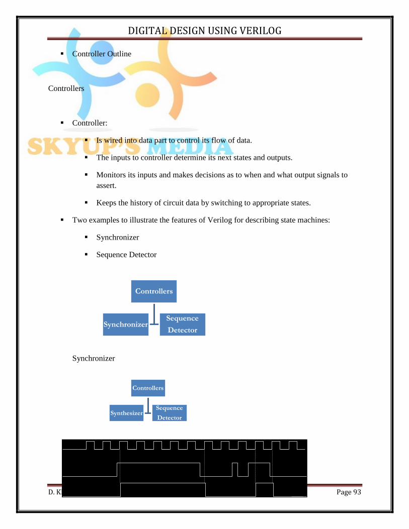
DIGITAL DESIGN USING VERILOG
D. KHALANDAR BASHA, ASSOC. PROF., IARE Page 93
Controller Outline
Controllers
Controller:
Is wired into data part to control its flow of data.
The inputs to controller determine its next states and outputs.
Monitors its inputs and makes decisions as to when and what output signals to
assert.
Keeps the history of circuit data by switching to appropriate states.
Two examples to illustrate the features of Verilog for describing state machines:
Synchronizer
Sequence Detector
Synchronizer
Controllers
Synchronizer Sequence
Detector
Controllers
Synthesizer Sequence
Detector
Clk
adata
synched
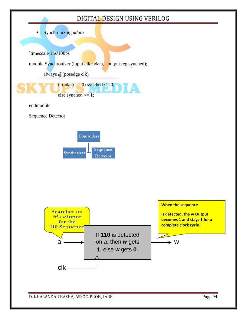
DIGITAL DESIGN USING VERILOG
D. KHALANDAR BASHA, ASSOC. PROF., IARE Page 94
Synchronizing adata
`timescale 1ns/100ps
module Synchronizer (input clk, adata, output reg synched);
always @(posedge clk)
if (adata == 0) synched <= 0;
else synched <= 1;
endmodule
Sequence Detector
Controllers
Synthesizer Sequence
Detector
If 110 is detected
on a, then w gets
1, else w gets 0.
clk
a w
When the sequence
is detected, the w Output becomes 1 and stays 1 for a complete clock cycle
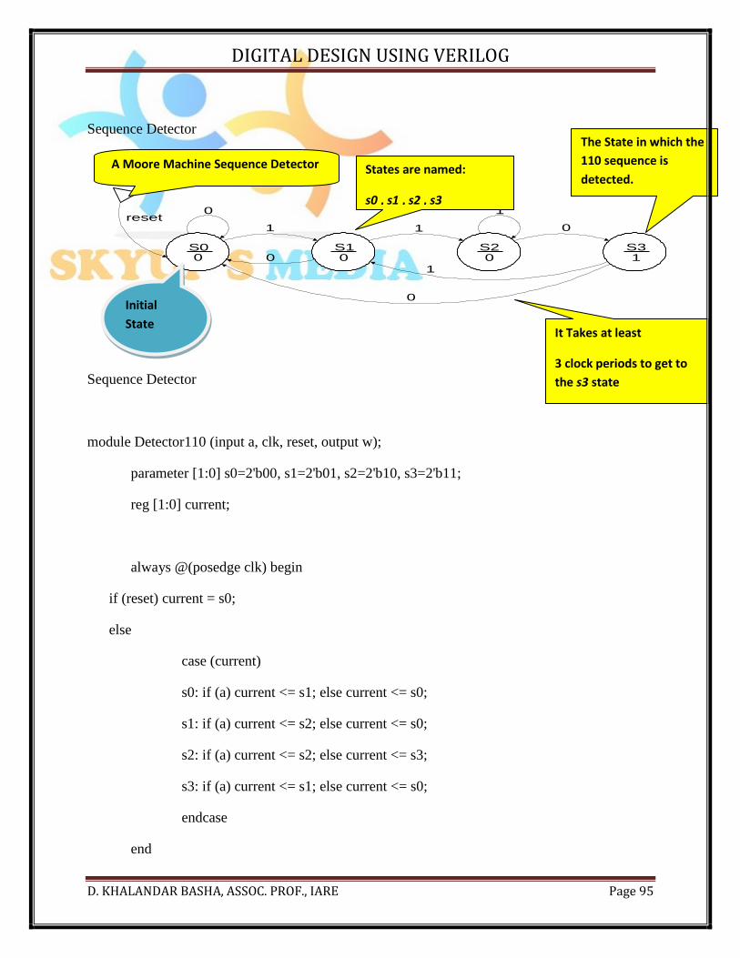
DIGITAL DESIGN USING VERILOG
D. KHALANDAR BASHA, ASSOC. PROF., IARE Page 95
Sequence Detector
Sequence Detector
module Detector110 (input a, clk, reset, output w);
parameter [1:0] s0=2'b00, s1=2'b01, s2=2'b10, s3=2'b11;
reg [1:0] current;
always @(posedge clk) begin
if (reset) current = s0;
else
case (current)
s0: if (a) current <= s1; else current <= s0;
s1: if (a) current <= s2; else current <= s0;
s2: if (a) current <= s2; else current <= s3;
s3: if (a) current <= s1; else current <= s0;
endcase
end
01
1
1
0
0
1
0reset
S00 0 10
S1 S2 S3
A Moore Machine Sequence Detector
Initial
State
States are named:
s0 , s1 , s2 , s3
The State in which the
110 sequence is
detected.
It Takes at least
3 clock periods to get to
the s3 state

DIGITAL DESIGN USING VERILOG
D. KHALANDAR BASHA, ASSOC. PROF., IARE Page 96
assign w = (current == s3) ? 1 : 0;
endmodule
Verilog Code for 110 Detector
State Machine Coding
Moore Machines
State Machine
Coding
Moore Machines Mealy Machines
Huffman
Coding Style
A More Modular
Style
A ROM Based
Controller
State Machine
Coding
Moore Machines Mealy Machines
Huffman
Coding Style
A More Modular
Style
A ROM Based
Controller
Moore
Machines

DIGITAL DESIGN USING VERILOG
D. KHALANDAR BASHA, ASSOC. PROF., IARE Page 97
Moore Machines
Moore Machine :
A state machine in which all outputs are carefully synchronized with the circuit
clock.
In the state diagram form, each state of the machine specifies its outputs
independent of circuit inputs.
In Verilog code of a state machine, only circuit state variables participate in the
output expression of the circuit.
Mealy Machines
Mealy Machines
1. Mealy Machine :
1. Is different from a Moore machine in that its output depends on its current state
and inputs while in that state.
2. State transitions and clocking and resetting the machine are no different from
those of a Moore machine. The same coding techniques are used.
State Machine
Coding
Moore Machines Mealy Machines
Huffman
Coding Style
A More Modular
Style
A ROM Based
Controller
Mealy
Machines
Top Related