


Languages
Pages
Legal


270
C H A P T E R
7
D E S I G N I N G S E Q U E N T I A L L O G I CC I R C U I T S
Implementation techniques for flip-flops, latches, oscillators, pulse generators,
n
and Schmitt triggers
n
Static versus dynamic realization
Choosing clocking strategies
7.1 Introduction
7.2 Timing Metrics for Sequential Circuits
7.3 Classification of Memory Elements
7.4 Static Latches and Registers
7.4.1The Bistability Principle
7.4.2SR Flip-Flops
7.4.3Multiplexer Based Latches
7.4.4Master-Slave Based Edge TriggeredRegister
7.4.5Non-ideal clock signals
7.4.6Low-Voltage Static Latches
7.5 Dynamic Latches and Registers
7.5.1 Dynamic Transmission-Gate BasedEdge-triggred Registers
7.5.2 C2MOS Dynamic Register: A ClockSkew Insensitive Approach
7.5.3 True Single-Phase Clocked Register(TSPCR)
7.6 Pulse Registers
6.4.2 The C2MOS Latch
7.8.2 NORA-CMOS—A Logic Style forPipelined Structures
7.5.3 True Single-Phase Clocked Register(TSPCR)
7.7 Sense-Amplifier Based Registers
7.8 Pipelining: An approach to optimize sequentialcircuits
chapter7_pub.fm Page 270 Wednesday, November 22, 2000 8:41 AM

Section 271
7.8.1Latch- vs. Register-Based Pipelines
7.8.2NORA-CMOS—A Logic Style for Pipelined Structures
7.9 Non-Bistable Sequential Circuits
7.9.1The Schmitt Trigger
7.9.2Monostable Sequential Circuits
7.9.3Astable Circuits
7.10 Perspective: Choosing a Clocking Strategy
7.11 Summary
7.12 To Probe Further
7.13 Exercises and Design Problems
chapter7_pub.fm Page 271 Wednesday, November 22, 2000 8:41 AM

272 DESIGNING SEQUENTIAL LOGIC CIRCUITS Chapter 7
7.1 Introduction
Combinational logic circuits that were described earlier have the property that the outputof a logic block is only a function of the current input values, assuming that enough timehas elapsed for the logic gates to settle. Yet virtually all useful systems require storage ofstate information, leading to another class of circuits called sequential logic circuits. Inthese circuits, the output not only depends upon the current values of the inputs, but alsoupon preceding input values. In other words, a sequential circuit remembers some of thepast history of the system—it has memory.
Figure 7.1 shows a block diagram of a generic finite state machine (FSM) that con-sists of combinational logic and registers that hold the system state. The system depictedhere belongs to the class of synchronous sequential systems, in which all registers areunder control of a single global clock. The outputs of the FSM are a function of the currentInputs and the Current State. The Next State is determined based on the Current State andthe current Inputs and is fed to the inputs of registers. On the rising edge of the clock, theNext State bits are copied to the outputs of the registers (after some propagation delay),and a new cycle begins. The register then ignores changes in the input signals until thenext rising edge. In general, registers can be positive edge-triggered (where the input datais copied on the positive edge) or negative edge-triggered (where the input data is copiedon the negative edge of the clock, as is indicated by a small circle at the clock input).
This chapter discusses the CMOS implementation of the most important sequentialbuilding blocks. A variety of choices in sequential primitives and clocking methodologiesexist; making the correct selection is getting increasingly important in modern digital cir-cuits, and can have a great impact on performance, power, and/or design complexity.Before embarking on a detailed discussion on the various design options, a revision of thedesign metrics, and a classification of the sequential elements is necessary.
7.2 Timing Metrics for Sequential Circuits
There are three important timing parameters associated with a register as illustrated in Fig-ure 7.2. The set-up time (tsu) is the time that the data inputs (D input) must be valid beforethe clock transition (this is, the 0 to 1 transition for a positive edge-triggered register). Thehold time (thold) is the time the data input must remain valid after the clock edge. Assum-
CLK
Figure 7.1 Block diagram of a finite state machine using positive edge-triggered registers.
DQ
Inputs OutputsCOMBINATIONAL
LOGIC
RegistersCurrent State Next State
chapter7_pub.fm Page 272 Wednesday, November 22, 2000 8:41 AM

Section 7.3 Classification of Memory Elements 273
ing that the set-up and hold-times are met, the data at the D input is copied to the Q outputafter a worst-case propagation delay (with reference to the clock edge) denoted by tc-q.
Given the timing information for the registers and the combination logic, some sys-tem-level timing constraints can be derived. Assume that the worst-case propagationdelay of the logic equals tplogic, while its minimum delay (also called the contaminationdelay) is tcd. The minimum clock period T, required for proper operation of the sequentialcircuit is given by
(7.1)
The hold time of the register imposes an extra constraint for proper operation,
(7.2)
where tcdregister is the minimum propagation delay (or contamination delay) of the register.As seen from Eq. (7.1), it is important to minimize the values of the timing parame-
ters associated with the register, as these directly affect the rate at which a sequential cir-cuit can be clocked. In fact, modern high-performance systems are characterized by avery-low logic depth, and the register propagation delay and set-up times account for asignificant portion of the clock period. For example, the DEC Alpha EV6 microprocessor[Gieseke97] has a maximum logic depth of 12 gates, and the register overhead stands forapproximately 15% of the clock period. In general, the requirement of Eq. (7.2) is not hardto meet, although it becomes an issue when there is little or no logic between registers, (orwhen the clocks at different registers are somewhat out of phase due to clock skew, as willbe discussed in a later Chapter).
7.3 Classification of Memory Elements
Foreground versus Background Memory
At a high level, memory is classified into background and foreground memory. Memorythat is embedded into logic is foreground memory, and is most often organized as individ-ual registers of register banks. Large amounts of centralized memory core are referred toas background memory. Background memory, discussed later in this book, achieves
DATASTABLE
DATASTABLE
D
Q
t
t
t
tsu thold
tc-q
Figure 7.2 Definition of set-uptime, hold time, and propagationdelay of a synchronous register.
CLK
CLK
QD
Register
T tc-q tp iclog tsu+ +≥
tcdregister tcd logic+ thold≥
chapter7_pub.fm Page 273 Wednesday, November 22, 2000 8:41 AM

274 DESIGNING SEQUENTIAL LOGIC CIRCUITS Chapter 7
higher area densities through efficient use of array structures and by trading off perfor-mance and robustness for size. In this chapter, we focus on foreground memories.
Static versus Dynamic Memory
Memories can be static or dynamic. Static memories preserve the state as long as thepower is turned on. Static memories are built using positive feedback or regeneration,where the circuit topology consists of intentional connections between the output and theinput of a combinational circuit. Static memories are most useful when the register won’tbe updated for extended periods of time. An example of such is configuration data, loadedat power-up time. This condition also holds for most processors that use conditional clock-ing (i.e., gated clocks) where the clock is turned off for unused modules. In that case, thereare no guarantees on how frequently the registers will be clocked, and static memories areneeded to preserve the state information. Memory based on positive feedback fall underthe class of elements called multivibrator circuits. The bistable element, is its most popu-lar representative, but other elements such as monostable and astable circuits are also fre-quently used.
Dynamic memories store state for a short period of time—on the order of millisec-onds. They are based on the principle of temporary charge storage on parasitic capacitorsassociated with MOS devices. As with dynamic logic discussed earlier, the capacitorshave to be refreshed periodically to annihilate charge leakage. Dynamic memories tend tosimpler, resulting in significantly higher performance and lower power dissipation. Theyare most useful in datapath circuits that require high performance levels and are periodi-cally clocked. It is possible to use dynamic circuitry even when circuits are conditionallyclocked, if the state can be discarded when a module goes into idle mode.
Latches vs. Registers
A latch is an essential component in the construction of an edge-triggered register. It islevel-sensitive circuit that passes the D input to the Q output when the clock signal is high.This latch is said to be in transparent mode. When the clock is low, the input data sampledon the falling edge of the clock is held stable at the output for the entire phase, and thelatch is in hold mode. The inputs must be stable for a short period around the falling edgeof the clock to meet set-up and hold requirements. A latch operating under the above con-ditions is a positive latch. Similarly, a negative latch passes the D input to the Q outputwhen the clock signal is low. The signal waveforms for a positive and negative latch areshown in Figure 7.3. A wide variety of static and dynamic implementations exists for therealization of latches.
Contrary to level-sensitive latches, edge-triggered registers only sample the input ona clock transition — 0-to-1 for a positive edge-triggered register, and 1-to-0 for a negativeedge-triggered register. They are typically built using the latch primitives of Figure 7.3. Amost-often recurring configuration is the master-slave structure that cascades a positiveand negative latch. Registers can also be constructed using one-shot generators of theclock signal (“glitch” registers), or using other specialized structures. Examples of theseare shown later in this chapter.
chapter7_pub.fm Page 274 Wednesday, November 22, 2000 8:41 AM

Section 7.4 Static Latches and Registers 275
7.4 Static Latches and Registers
7.4.1 The Bistability Principle
Static memories use positive feedback to create a bistable circuit — a circuit having twostable states that represent 0 and 1. The basic idea is shown in Figure 7.4a, which showstwo inverters connected in cascade along with a voltage-transfer characteristic typical ofsuch a circuit. Also plotted are the VTCs of the first inverter, that is, Vo1 versus Vi1, and thesecond inverter (Vo2 versus Vo1). The latter plot is rotated to accentuate that Vi2 = Vo1.Assume now that the output of the second inverter Vo2 is connected to the input of the firstVi1, as shown by the dotted lines in Figure 7.4a. The resulting circuit has only three possi-
CLK
QD
CLK
QD
clk
In
Out
G
In Out In Out
Figure 7.3 Timing of positive and negative latches.
Positive Latch Negative Latch
G
clk
In
Out
Outstable
Outfollows In
Outstable
Outfollows In
Figure 7.4 Two cascaded inverters (a)and their VTCs (b).
Vi1Vo1 = Vi2 Vo2
Vi1 Vo2
Vo1
Vi2
=V
o1
Vi2
=V
o1
Vi1 = Vo2
A
C
B
Vo2 = Vi1
(a)
(b)
chapter7_pub.fm Page 275 Wednesday, November 22, 2000 8:41 AM

276 DESIGNING SEQUENTIAL LOGIC CIRCUITS Chapter 7
ble operation points (A, B, and C), as demonstrated on the combined VTC. The followingimportant conjecture is easily proven to be valid:
Under the condition that the gain of the inverter in the transient region is larger than 1, only Aand B are stable operation points, and C is a metastable operation point.
Suppose that the cross-coupled inverter pair is biased at point C. A small deviation fromthis bias point, possibly caused by noise, is amplified and regenerated around the circuitloop. This is a consequence of the gain around the loop being larger than 1. The effect isdemonstrated in Figure 7.5a. A small deviation δ is applied to Vi1 (biased in C). This devi-ation is amplified by the gain of the inverter. The enlarged divergence is applied to the sec-ond inverter and amplified once more. The bias point moves away from C until one of theoperation points A or B is reached. In conclusion, C is an unstable operation point. Everydeviation (even the smallest one) causes the operation point to run away from its originalbias. The chance is indeed very small that the cross-coupled inverter pair is biased at Cand stays there. Operation points with this property are termed metastable.
On the other hand, A and B are stable operation points, as demonstrated in Figure7.5b. In these points, the loop gain is much smaller than unity. Even a rather large devi-ation from the operation point is reduced in size and disappears.
Hence the cross-coupling of two inverters results in a bistable circuit, that is, a cir-cuit with two stable states, each corresponding to a logic state. The circuit serves as amemory, storing either a 1 or a 0 (corresponding to positions A and B).
In order to change the stored value, we must be able to bring the circuit from state Ato B and vice-versa. Since the precondition for stability is that the loop gain G is smallerthan unity, we can achieve this by making A (or B) temporarily unstable by increasing G toa value larger than 1. This is generally done by applying a trigger pulse at Vi1 or Vi2. Forinstance, assume that the system is in position A (Vi1 = 0, Vi2 = 1). Forcing Vi1 to 1 causesboth inverters to be on simultaneously for a short time and the loop gain G to be largerthan 1. The positive feedback regenerates the effect of the trigger pulse, and the circuitmoves to the other state (B in this case). The width of the trigger pulse need be only a little
Figure 7.5 Metastability.
Vi2
=V o
1
Vi1 = Vo2
C
Vi2
=V o
1
Vi1 = Vo2
A
δ δ
(a) (b)
A
B
C
B
chapter7_pub.fm Page 276 Wednesday, November 22, 2000 8:41 AM

Section 7.4 Static Latches and Registers 277
larger than the total propagation delay around the circuit loop, which is twice the averagepropagation delay of the inverters.
In summary, a bistable circuit has two stable states. In absence of any triggering, thecircuit remains in a single state (assuming that the power supply remains applied to thecircuit), and hence remembers a value. A trigger pulse must be applied to change the stateof the circuit. Another common name for a bistable circuit is flip-flop (unfortunately, anedge-triggered register is also referred to as a flip-flop).
7.4.2 SR Flip-Flops
The cross-coupled inverter pair shown in the previous section provides an approach tostore a binary variable in a stable way. However, extra circuitry must be added to enablecontrol of the memory states. The simplest incarnation accomplishing this is the well-know SR —or set-reset— flip-flop, an implementation of which is shown in Figure 7.6a.This circuit is similar to the cross-coupled inverter pair with NOR gates replacing theinverters. The second input of the NOR gates is connected to the trigger inputs (S and R),that make it possible to force the outputs Q and Q to a given state. These outputs are com-plimentary (except for the SR = 11 state). When both S and R are 0, the flip-flop is in a qui-escent state and both outputs retain their value (a NOR gate with one of its input being 0looks like an inverter, and the structure looks like a cross coupled inverter). If a positive(or 1) pulse is applied to the S input, the Q output is forced into the 1 state (with Q going to0). Vice versa, a 1 pulse on R resets the flip-flop and the Q output goes to 0.
These results are summarized in the characteristic table of the flip-flop, shown inFigure 7.6c. The characteristic table is the truth table of the gate and lists the output statesas functions of all possible input conditions. When both S and R are high, both Q and Qare forced to zero. Since this does not correspond with our constraint that Q and Q must becomplementary, this input mode is considered to be forbidden. An additional problemwith this condition is that when the input triggers return to their zero levels, the resultingstate of the latch is unpredictable and depends on whatever input is last to go low. Finally,Figure 7.6 shows the schematics symbol of the SR flip-flop.
Figure 7.6 NOR-based SR flip-flop.
S
R
Q
Q
QS
R Q
S R Q Q
0
1
0
1
0
0
11
Q
1
0
0
Q
0
10
(a) Schematic diagram (b) Logic symbol (c) Characteristic table
Forbidden State
chapter7_pub.fm Page 277 Wednesday, November 22, 2000 8:41 AM

278 DESIGNING SEQUENTIAL LOGIC CIRCUITS Chapter 7
Problem 7.1 SR Flip-Flop Using NAND Gates
An SR flip-flop can also be implemented using across-coupled NAND structure as shown in Figure7.7. Derive the truth table for a such an implemen-tation.
The SR flip-flops discussed so far are asynchronous, and do not require a clock sig-nal. Most systems operate in a synchronous fashion with transition events referenced to aclock. One possible realization of a clocked SR flip-flop— a level-sensitive positivelatch— is shown in Figure 7.8. It consists of a cross-coupled inverter pair, plus 4 extratransistors to drive the flip-flop from one state to another and to provide clocked opera-tion. Observe that the number of transistors is identical to the implementation of Figure7.6, but the circuit has the added feature of being clocked. The drawback of saving sometransistors over a fully-complimentary CMOS implementation is that transistor sizingbecomes critical in ensuring proper functionality. Consider the case where Q is high andan R pulse is applied. The combination of transistors M4, M7, and M8 forms a ratioedinverter. In order to make the latch switch, we must succeed in bringing Q below theswitching threshold of the inverter M1-M2. Once this is achieved, the positive feedbackcauses the flip-flop to invert states. This requirement forces us to increase the sizes of tran-sistors M5, M6, M7, and M8.
The presented flip-flop does not consume any static power. In steady-state, oneinverter resides in the high state, while the other one is low. No static paths between VDDand GND can exist except during switching.
Example 7.1 Transistor Sizing of Clocked SR Latch
Assume that the cross-coupled inverter pair is designed such that the inverter threshold VM islocated at VDD/2. For a 0.25 µm CMOS technology, the following transistor sizes wereselected: (W/L)M1 = (W/L)M3 = (0.5µm/0.25µm), and (W/L)M2 = (W/L)M4 = (1.5µm/0.25µm).Assuming Q = 0, we determine the minimum sizes of M5, M6, M7, and M8 to make the deviceswitchable.
Figure 7.7 NAND-based SR flip-flop.
S
R
Q
Q
VDD
RS
CLKCLK
Figure 7.8 CMOS clocked SR flip-flop.
M1 M3
M4M2
M6
M5 M7
M8
chapter7_pub.fm Page 278 Wednesday, November 22, 2000 8:41 AM

Section 7.4 Static Latches and Registers 279
To switch the latch from the Q = 0 to the Q = 1 state, it is essential that the low level ofthe ratioed, pseudo-NMOS inverter (M5-M6)-M2 be below the switching threshold of theinverter M3-M4 that equals VDD/2. It is reasonable to assume that as long as VQ > VM, VQ
equals 0, and the gate of transistor M2 is grounded. The boundary conditions on the transistorsizes can be derived by equating the currents in the inverter for VQ = VDD / 2, as given in Eq.(7.3) (this ignores channel length modulation). The currents are determined by the saturationcurrent since VSET = VDD = 2.5V and VM = 1.25V. We assume that M5 and M6 have identicalsizes and that W/L5-6 is the effective ratio of the series-connected devices. Under this condi-tion, the pull-down network can be modeled by a single transistor M56, whose length is twicethe length of the individual devices.
(7.3)
Using the parameters for the 0.25 µm process, Eq. (7.3) results in the constraint that theeffective (W/L)M5-6 ≥ 2.26. This implies that the individual device ratio for M5 or M6 must belarger that approximately 4.5. Figure 7.9a shows the DC plot of VQ as a function of the indi-vidual device sizes of M5 and M6. We notice that the individual device ratio of greater than 3is sufficient to bring the Q voltage to the inverter switching threshold. The difference betweenthe manual analysis and simulation arises due to second order effects such as DIBL and chan-nel length modulation. Figure 7.9b, which shows the transient response for different devicesizes. The plot confirms that an individual W/L ratio of greater than 3 is required to overpowerthe feedback and switch the state of the latch.
The positive feedback effect makes a manual derivation of propagation delay of theSR latch non-trivial. Some simplifications are therefore necessary. Consider, for instance,the latch of Figure 7.8, where Q and Q are set to 0 and 1, respectively. A pulse is applied atnode S, causing the latch to toggle. In the first phase of the transient, node Q is beingpulled down by transistors M5 and M6. Since node Q is initially low, the PMOS device M2is on while M1 is off. The transient response is hence determined by the pseudo-NMOSinverter formed by (M5-M6) and M2. Once Q reaches the switching threshold of the CMOSinverter M3-M4, this inverter reacts and the positive feedback comes into action, turningM2 off and M1 on. This accelerates the pulling down of node Q. From this analysis, we can
k ′nWL-----
5 6–VDD VTn–( )VDSATn
VDSATn2
2-----------------–
k ′pWL-----
2VDD– VTp–( )VDSATp
VDSATp2
2-----------------–
=
2.0 2.5 3.0 3.5 4.0W/L5and 6
0.0
0.5
1.0
1.5
2.0
Q(V
olts
)
Figure 7.9 Sizing issues for SR flip-flop. (a) DC output voltage vs. individual pulldowndevice size of M5 and M6 with W/L2= 1.5µm/.25µm. (b) Transient response shows that M5and M6 must each have a W/L larger than 3 to swtich the SR flip-flop.
0 1 2time (nsec)
0
1
2
3
Vol
ts
0.2 0.4 0.6 0.8 1.2 1.4 1.6 1.8
W=0.5µm
Q S
W=0.6µmW=0.7µm
W=0.8µm
W=0.9µmW=1µm
(a) (b)
chapter7_pub.fm Page 279 Wednesday, November 22, 2000 8:41 AM
280 DESIGNING SEQUENTIAL LOGIC CIRCUITS Chapter 7
derive that the propagation delay of node Q is approximately equal to the delay of thepseudo-NMOS inverter formed by (M5-M6) and M2. To obtain the delay for node Q, it issufficient to add the delay of the complementary CMOS inverter M3-M4.
Example 7.2 Propagation Delay of Static SR Flip-Flop
The transient response of the latch in Figure 7.8, as obtained from simulation, is plotted inFigure 7.10. The devices are sized as described in Example 7.1, and a load of a single inverteris assumed for each latch output. The flip-flop is initially in the reset state, and an S-pulse isapplied. As we can observe, this results first in a discharging of the Q output while Q stays at0. Once the switching threshold of the inverter M3-M4 is reached, the Q output starts to rise.The delay of this transient is solely determined by the M3-M4 inverter, which is hampered bythe slow rise time at its input. From the simulation results, we can derive that tpQ and tpQ equal120psec and 230psec, respectively.
Problem 7.2 Complimentary CMOS SR FF
Instead of using the modified SR FF of Figure 7.8, it is also possible to use complementarylogic to implement the clocked SR FF. Derive the transistor schematic (which consists of 12transistors). This circuit is more complex, but switches faster and consumes less switchingpower. Explain why.
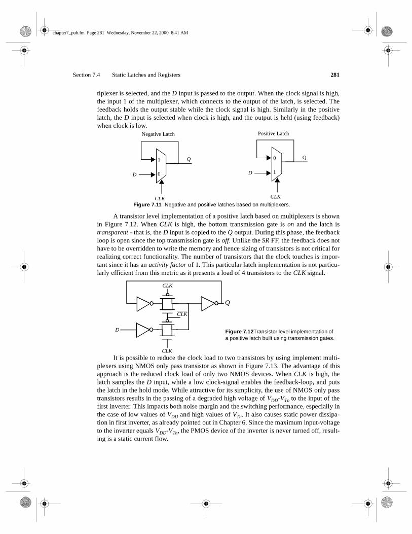
7.4.3 Multiplexer Based Latches
There are many approaches for constructing latches. One very common techniqueinvolves the use of transmission gate multiplexers. Multiplexer based latches can providesimilar functionality to the SR latch, but has the important added advantage that the sizingof devices only affects performance and is not critical to the functionality.
Figure 7.11 shows an implementation of static positive and negative latches basedon multiplexers. For a negative latch, when the clock signal is low, the input 0 of the mul-
Figure 7.10 Transient responseof SR flip-flop.
0.9 1.1 1.3 1.5
Time (ns)
0.0
1.0
2.0
3.0
Vol
ts
1.0 1.2 1.4
Q QSET
tpQ tpQ
chapter7_pub.fm Page 280 Wednesday, November 22, 2000 8:41 AM
Section 7.4 Static Latches and Registers 281
tiplexer is selected, and the D input is passed to the output. When the clock signal is high,the input 1 of the multiplexer, which connects to the output of the latch, is selected. Thefeedback holds the output stable while the clock signal is high. Similarly in the positivelatch, the D input is selected when clock is high, and the output is held (using feedback)when clock is low.
A transistor level implementation of a positive latch based on multiplexers is shownin Figure 7.12. When CLK is high, the bottom transmission gate is on and the latch istransparent - that is, the D input is copied to the Q output. During this phase, the feedbackloop is open since the top transmission gate is off. Unlike the SR FF, the feedback does nothave to be overridden to write the memory and hence sizing of transistors is not critical forrealizing correct functionality. The number of transistors that the clock touches is impor-tant since it has an activity factor of 1. This particular latch implementation is not particu-larly efficient from this metric as it presents a load of 4 transistors to the CLK signal.
It is possible to reduce the clock load to two transistors by using implement multi-plexers using NMOS only pass transistor as shown in Figure 7.13. The advantage of thisapproach is the reduced clock load of only two NMOS devices. When CLK is high, thelatch samples the D input, while a low clock-signal enables the feedback-loop, and putsthe latch in the hold mode. While attractive for its simplicity, the use of NMOS only passtransistors results in the passing of a degraded high voltage of VDD-VTn to the input of thefirst inverter. This impacts both noise margin and the switching performance, especially inthe case of low values of VDD and high values of VTn. It also causes static power dissipa-tion in first inverter, as already pointed out in Chapter 6. Since the maximum input-voltageto the inverter equals VDD-VTn, the PMOS device of the inverter is never turned off, result-ing is a static current flow.
0
1
CLK
D
Q
1
0
CLK
D
Q
Negative Latch Positive Latch
Figure 7.11 Negative and positive latches based on multiplexers.
Q
D
CLK
CLK
CLK
Figure 7.12Transistor level implementation ofa positive latch built using transmission gates.
chapter7_pub.fm Page 281 Wednesday, November 22, 2000 8:41 AM

282 DESIGNING SEQUENTIAL LOGIC CIRCUITS Chapter 7
7.4.4 Master-Slave Based Edge Triggered Register
The most common approach for constructing an edge-triggered register is to use amaster-slave configuration as shown in Figure 7.14. The register consists of cascading anegative latch (master stage) with a positive latch (slave stage). A multiplexer based latchis used in this particular implementation, though any latch can be used to realize the mas-ter and slave stages. On the low phase of the clock, the master stage is transparent and theD input is passed to the master stage output, QM. During this period, the slave stage is inthe hold mode, keeping its previous value using feedback. On the rising edge of the clock,the master slave stops sampling the input, and the slave stage starts sampling. During thehigh phase of the clock, the slave stage samples the output of the master stage (QM), whilethe master stage remains in a hold mode. Since QM is constant during the high phase of theclock, the output Q makes only one transition per cycle. The value of Q is the value of Dright before the rising edge of the clock, achieving the positive edge-triggered effect. Anegative edge-triggered register can be constructed using the same principle by simplyswitching the order of the positive and negative latch (i.e., placing the positive latch first).
A complete transistor level implementation of a the master-slave positive edge-trig-gered register is shown in Figure 7.15. The multiplexer is implemented using transmissiongates as discussed in the previous section. When clock is low (CLK = 1), T1 is on and T2 isoff, and the D input is sampled onto node QM. During this period, T3 is off and T4 is on andthe cross-coupled inverters (I5, I6) holds the state of the slave latch. When the clock goeshigh, the master stage stops sampling the input and goes into a hold mode. T1 is off and T2
QM
CLK
CLK
D
(a) Schematic diagram (b) Nonoverlapping clocks
Figure 7.13 Multiplexer based NMOS latch using NMOS only pass transistors for multiplexers.
CLK
CLK
QM
Figure 7.14 Positive edge-triggered register based on a master-slave configuration.
0
1
CLK
D
1
0
CLK
Q
CLK
D
QM
Q
Master
Slave
QM
chapter7_pub.fm Page 282 Wednesday, November 22, 2000 8:41 AM

Section 7.4 Static Latches and Registers 283
is on, and the cross coupled inverters I3 and I4 holds the state of QM. Also, T3 is on and T4is off, and QM is copied to the output Q.
Problem 7.3Optimization of the Master Slave Register
It is possible to remove the inverters I1 and I2 from Figure 7.3 without loss of functionality.Is there any advantage in including these inverters in the implementation?
Timing Properties of the multiplexer Bases Master-Slave Register. As discussed ear-lier, there are three important timing metrics in registers: the set up time, the hold time andthe propagation delay. It is important to understand these factors that affect the timingparameters and develop the intuition to manually estimate the parameters. Assume that thepropagation delay of each inverter is tpd_inv and the propagation delay of the transmissiongate is tpd_tx. Also assume that the contamination delay is 0 and the inverter delay to deriveCLK from CLK has a delay equal to 0.
The set-up time is the time before the rising edge of the clock that the input data Dmust become valid. Another way to ask the question is how long before the rising edgedoes the D input have to be stable such that QM samples the value reliably. For the trans-mission gate multiplexer-based register, the input D has to propagate through I1, T1, I3 andI2 before the rising edge of the clock. This is to ensure that the node voltages on both ter-minals of the transmission gate T2 are at the same value. Otherwise, it is possible for thecross-coupled pair I2 and I3 to settle to an incorrect value. The set-up time is thereforeequal to 3 *tpd_inv + tpd_tx .
The propagation delay is the time for the value of QM to propagate to the output Q.Note that since we included the delay of I2 in the set-up time, the output of I4 is validbefore the rising edge of clock. Therefore the delay tc-q is simply the delay through T3 andI6 (tc-q = tpd_tx + tpd_inv).
The hold time represents the time that the input must be held stable after the risingedge of the clock. In this case, the transmission gate T1 turns off when clock goes high andtherefore any changes in the D-input after clock going high are not seen by the input.Therefore, the hold time is 0.
Figure 7.15 Transistor-level implementation of a master-slave postive edge-triggeredregister using multiplexers.
D
CLK
Q
QM
T1
T2 T4
T3I1
I2 I3I5 I6
I4
chapter7_pub.fm Page 283 Wednesday, November 22, 2000 8:41 AM
284 DESIGNING SEQUENTIAL LOGIC CIRCUITS Chapter 7
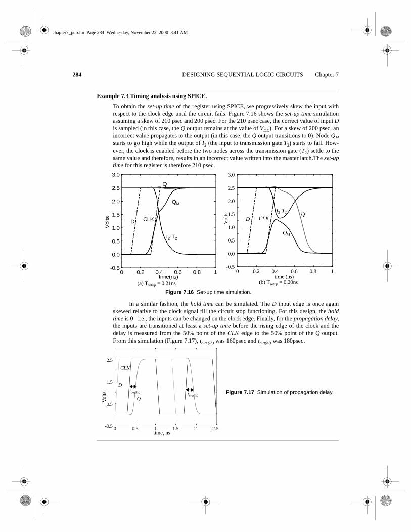
Example 7.3 Timing analysis using SPICE.
To obtain the set-up time of the register using SPICE, we progressively skew the input withrespect to the clock edge until the circuit fails. Figure 7.16 shows the set-up time simulationassuming a skew of 210 psec and 200 psec. For the 210 psec case, the correct value of input Dis sampled (in this case, the Q output remains at the value of VDD). For a skew of 200 psec, anincorrect value propagates to the output (in this case, the Q output transitions to 0). Node QM
starts to go high while the output of I2 (the input to transmission gate T2) starts to fall. How-ever, the clock is enabled before the two nodes across the transmission gate (T2) settle to thesame value and therefore, results in an incorrect value written into the master latch.The set-uptime for this register is therefore 210 psec.
In a similar fashion, the hold time can be simulated. The D input edge is once againskewed relative to the clock signal till the circuit stop functioning. For this design, the holdtime is 0 - i.e., the inputs can be changed on the clock edge. Finally, for the propagation delay,the inputs are transitioned at least a set-up time before the rising edge of the clock and thedelay is measured from the 50% point of the CLK edge to the 50% point of the Q output.From this simulation (Figure 7.17), tc-q (lh) was 160psec and tc-q(hl) was 180psec.
0 0.2 0.4 0.6 0.8 1time (ns)
-0.5
0.0
0.5
1.0
1.5
2.0
2.5
3.0
0 0.2 0.4 0.6 0.8 1time(ns)
-0.5
0.0
0.5
1.0
1.5
2.0
2.5
3.0
Vol
ts CLKD
QM
Q
CLKDQ
QM
I2-T2
I2-T2
(a) Tsetup = 0.21ns (b) Tsetup = 0.20ns
Figure 7.16 Set-up time simulation.
Vol
ts
Figure 7.17 Simulation of propagation delay.Q
D
CLK
tc-q(lh) tc-q(hl)
0 0.5 1 1.5 2 2.5-0.5
0.5
1.5
2.5
time, ns
Vol
ts
chapter7_pub.fm Page 284 Wednesday, November 22, 2000 8:41 AM

Section 7.4 Static Latches and Registers 285
As mentioned earlier, the drawback of the transmission gate register is the high capacitiveload presented to the clock signal. The clock load per register is important since it directlyimpacts the power dissipation of the clock network. Ignoring the overhead required toinvert the clock signal (since the buffer inverter overhead can be amortized over multipleregister bits), each register has a clock load of 8 transistors. One approach to reduce theclock load at the cost of robustness is to make the circuit ratioed. Figure 7.18 shows thatthe feedback transmission gate can be eliminated by directly cross coupling the inverters.
The penalty for the reduced clock load is increased design complexity. The trans-mission gate (T1) and its source driver must overpower the feedback inverter (I2) to switchthe state of the cross-coupled inverter.The sizing requirements for the transmission gatescan be derived using a similar analysis as performed for the SR flip-flop. The input to theinverter I1 must be brought below its switching threshold in order to make a transition. Ifminimum-sized devices are to be used in the transmission gates, it is essential that thetransistors of inverter I2 should be made even weaker. This can be accomplished by mak-ing their channel-lengths larger than minimum. Using minimum or close-to-minimum-size devices in the transmission gates is desirable to reduce the power dissipation in thelatches and the clock distribution network.
Another problem with this scheme is the reverse conduction — this is, the secondstage can affect the state of the first latch. When the slave stage is on (Figure 7.19), it ispossible for the combination of T2 and I4 to influence the data stored in I1-I2 latch. As longas I4 is a weak device, this is fortunately not a major problem.
7.4.5 Non-ideal clock signals
So far, we have assumed that CLK is a perfect inversion of CLK, or in other words, that thedelay of the generating inverter is zero. Even if this were possible, this would still not be agood assumption. Variations can exist in the wires used to route the two clock signals, or
D
CLK
CLK
CLK
CLK
Q
Figure 7.18 Reduced load clock load static master-slave register.
T1 I1
I2
T2 I3
I4
D
0
VDD
VDD
0
QT1I1
I2
T2I3
I4
Figure 7.19 Reverse conduction possible in the transmission gate.
chapter7_pub.fm Page 285 Wednesday, November 22, 2000 8:41 AM

286 DESIGNING SEQUENTIAL LOGIC CIRCUITS Chapter 7
the load capacitances can vary based on data stored in the connecting latches. This effect,known as clock skew is a major problem, and causes the two clock signals to overlap as isshown in Figure 7.20b. Clock-overlap can cause two types of failures, as illustrated for theNMOS-only negative master-slave register of Figure 7.20a.
• When the clock goes high, the slave stage should stop sampling the master stageoutput and go into a hold mode. However, since CLK and CLK are both high for ashort period of time (the overlap period), both sampling pass transistors conduct andthere is a direct path from the D input to the Q output. As a result, data at the outputcan change on the rising edge of the clock, which is undesired for a negative edge-triggered register. The is know as a race condition in which the value of the outputQ is a function of whether the input D arrives at node X before or after the fallingedge of CLK. If node X is sampled in the metastable state, the output will switch to avalue determined by noise in the system.
• The primary advantage of the multiplexer-based register is that the feedback loop isopen during the sampling period, and therefore sizing of devices is not critical tofunctionality. However, if there is clock overlap between CLK and CLK, node A canbe driven by both D and B, resulting in an undefined state.
Those problems can be avoided by using two non-overlapping clocks PHI1 and PHI2instead (Figure 7.21), and by keeping the nonoverlap time tnon_overlap between the clockslarge enough such that no overlap occurs even in the presence of clock-routing delays.During the nonoverlap time, the FF is in the high-impedance state—the feedback loop isopen, the loop gain is zero, and the input is disconnected. Leakage will destroy the state ifthis condition holds for too long a time. Hence the name pseudostatic: the registeremploys a combination of static and dynamic storage approaches depending upon the stateof the clock.
Q
D
(a) Schematic diagram
A
B
(b) Overlapping clock pairs
Figure 7.20 Master-slave register basedon NMOS-only pass transistors.
CLK
CLK
CLK
CLK
CLK
CLK
X
chapter7_pub.fm Page 286 Wednesday, November 22, 2000 8:41 AM

Section 7.4 Static Latches and Registers 287
Problem 7.4 Generating non-overlapping clocks
Figure 7.22 shows one possible implementation of the clock generation circuitry for generat-ing a two-phase non-overlapping clocks. Assuming that each gate has a unit gate delay, derivethe timing relationship between the input clock and the two output clocks. What is the non-overlap period? How can this period be increased if needed?
7.4.6 Low-Voltage Static Latches
The scaling of supply voltages is critical for low power operation. Unfortunately,certain latch structures don’t function at reduced supply voltages. For example, withoutthe scaling of device thresholds, NMOS only pass transistors (e.g., Figure 7.21) don’tscale well with supply voltage due to its inherent threshold drop. At very low power sup-ply voltages, the input to the inverter cannot be raised above the switching threshold,resulting in incorrect evaluation. Even with the use of transmission gates, performancedegrades significantly at reduced supply voltages.
Scaling to low supply voltages hence requires the use of reduced threshold devices.However, this has the negative effect of exponentially increasing the sub-threshold leak-age power as discussed in Chapter 6. When the registers are constantly accessed, the leak-
Figure 7.21 Pseudostatic two-phase D register.
Q
D
(a) Schematic diagram
tnon_overlap
(b) Two-phase nonoverlapping clocks
PHI2
PHI1
PHI2
PHI2
PHI1
PHI1
CLK
PHI1
PHI2
Figure 7.22Circuitry for generating atwo phase non-overlapping clock
chapter7_pub.fm Page 287 Wednesday, November 22, 2000 8:41 AM

288 DESIGNING SEQUENTIAL LOGIC CIRCUITS Chapter 7
age energy is typically insignificant compared to the switching power. However, with theuse of conditional clocks, it is possible that registers are idle for extended periods and theleakage energy expended by registers can be quite significant.
Many solutions are being explored to address the problem of high leakage duringidle periods. One approach for this involves the use of Multiple Threshold devices asshown in Figure 7.23 [Mutoh95]. Only the negative latch is shown here. The shadedinverters and transmission gates are implemented in low-threshold devices. The low-threshold inverters are gated using high threshold devices to eliminate leakage.
During normal mode of operation, the sleep devices are tuned on. When clock islow, the D input is sampled and propagates to the output. When clock is high, the latch isin the hold mode. The feedback transmission gate conducts and the cross-coupled feed-back is enabled. Note there is an extra inverter, needed for storage of state when the latchis in the sleep state. During idle mode, the high threshold devices in series with the lowthreshold inverter are turned off (the SLEEP signal is high), eliminating leakage. It isassumed that clock is in the high state when the latch is in the sleep state. The feedbacklow-threshold transmission gate is turned on and the cross-coupled high-threshold devicesmaintains the state of the latch.
Problem 7.5Transistor minimization in the MTCMOS register
Unlike combination logic, both flavors of high threshold devices in series are required toeliminate the leakage of low threshold gates. Explain why this is the case. Hint: Eliminatethe high VT NMOS or high VT PMOS of the low threshold inverter on the right of Figure7.23 and investigate potential leakage paths.
SLEEP High VT
SLEEP High VT
CLKSLEEP High VT
SLEEP High VT
Figure 7.23 One solution for the leakage problem in low-voltage operation using MTCMOS.
CLK
CLK
D Q
VDD
VDD
VDD
VDD
chapter7_pub.fm Page 288 Wednesday, November 22, 2000 8:41 AM
Section 7.5 Dynamic Latches and Registers 289
7.5 Dynamic Latches and Registers
Storage in a static sequential circuit relies on the concept that a cross-coupled inverter pairproduces a bistable element and can thus be used to memorize binary values. Thisapproach has the useful property that a stored value remains valid as long as the supplyvoltage is applied to the circuit, hence the name static. The major disadvantage of thestatic gate, however, is its complexity. When registers are used in computational structuresthat are constantly clocked such as pipelined datapath, the requirement that the memoryshould hold state for extended periods of time can be significantly relaxed.
This results in a class of circuits based on temporary storage of charge on parasiticcapacitors. The principle is exactly identical to the one used in dynamic logic — chargestored on a capacitor can be used to represent a logic signal. The absence of chargedenotes a 0, while its presence stands for a stored 1. No capacitor is ideal, unfortunately,and some charge leakage is always present. A stored value can hence only be kept for alimited amount of time, typically in the range of milliseconds. If one wants to preservesignal integrity, a periodic refresh of its value is necessary. Hence the name dynamic stor-age. Reading the value of the stored signal from a capacitor without disrupting the chargerequires the availability of a device with a high input impedance.
7.5.1 Dynamic Transmission-Gate Based Edge-triggred Registers
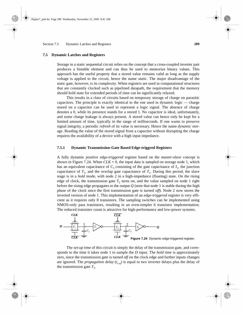
A fully dynamic positive edge-triggered register based on the master-slave concept isshown in Figure 7.24. When CLK = 0, the input data is sampled on storage node 1, whichhas an equivalent capacitance of C1 consisting of the gate capacitance of I1, the junctioncapacitance of T1, and the overlap gate capacitance of T1. During this period, the slavestage is in a hold mode, with node 2 in a high-impedance (floating) state. On the risingedge of clock, the transmission gate T2 turns on, and the value sampled on node 1 rightbefore the rising edge propagates to the output Q (note that node 1 is stable during the highphase of the clock since the first transmission gate is turned off). Node 2 now stores theinverted version of node 1. This implementation of an edge-triggered register is very effi-cient as it requires only 8 transistors. The sampling switches can be implemented usingNMOS-only pass transistors, resulting in an even-simpler 6 transistor implementation.The reduced transistor count is attractive for high-performance and low-power systems.
The set-up time of this circuit is simply the delay of the transmission gate, and corre-sponds to the time it takes node 1 to sample the D input. The hold time is approximatelyzero, since the transmission gate is turned off on the clock edge and further inputs changesare ignored. The propagation delay (tc-q) is equal to two inverter delays plus the delay ofthe transmission gate T2.
D
CLK
CLK
CLK
CLK
QT1 I1 T2 I3
Figure 7.24 Dynamic edge-triggered register.
C1 C2
1 2
chapter7_pub.fm Page 289 Wednesday, November 22, 2000 8:41 AM

290 DESIGNING SEQUENTIAL LOGIC CIRCUITS Chapter 7
One important consideration for such a dynamic register is that the storage nodes(i.e., the state) has to be refreshed at periodic intervals to prevent a loss due to charge leak-age, due to diode leakage as well as sub-threshold currents. In datapath circuits, the refreshrate is not an issue since the registers are periodically clocked, and the storage nodes areconstantly updated.
Clock overlap is an important concern for this register. Consider the clock wave-forms shown in Figure 7.25. During the 0-0 overlap period, the NMOS of T1 and thePMOS of T2 are simultaneously on, creating a direct path for data to flow from the D inputof the register to the Q output. This is known as a race condition. The output Q can changeon the falling edge if the overlap period is large — obviously an undesirable effect for apositive edge-triggered register. The same is true for the 1-1 overlap region, where aninput-output path exists through the PMOS of T1 and the NMOS of T2. The latter case istaken care off by enforcing a hold time constraint. That is, the data must be stable duringthe high-high overlap period. The former situation (0-0 overlap) can be addressed by mak-ing sure that there is enough delay between the D input and node 2 ensuring that new datasampled by the master stage does not propagate through to the slave stage. Generally thebuilt in single inverter delay should be sufficient and the overlap period constraint is givenas:
(7.4)
Similarly, the constraint for the 1-1 overlap is given as:
(7.5)
7.5.2 C2MOS Dynamic Register: A Clock Skew Insensitive Approach
The C2MOS Register
Figure 7.26 shows an ingenious positive edge-triggered register based on the master-slaveconcept which is insensitive to clock overlap. This circuit is called the C2MOS (ClockedCMOS) register [Suzuki73]. The register operates in two phases.
1. CLK = 0 (CLK = 1): The first tri-state driver is turned on, and the master stage actsas an inverter sampling the inverted version of D on the internal node X. The masterstage is in the evaluation mode. Meanwhile, the slave section is in a high-impedancemode, or in a hold mode. Both transistors M7 and M8 are off, decoupling the outputfrom the input. The output Q retains its previous value stored on the output capacitorCL2.
toverlap0 0– tT1 tI1 tT2+ +<
thold toverlap1 1–>
CLK
CLK
Figure 7.25 Impact of non-overlapping clocks.
(0,0) overlap
(1,1) overlap
chapter7_pub.fm Page 290 Wednesday, November 22, 2000 8:41 AM

Section 7.5 Dynamic Latches and Registers 291
2. The roles are reversed when CLK = 1: The master stage section is in hold mode (M3-M4 off), while the second section evaluates (M7-M8 on). The value stored on CL1propagates to the output node through the slave stage which acts as an inverter.
The overall circuit operates as a positive edge-triggered master-slave register —very similar to the transmission-gate based register presented earlier. However, there is animportant difference:
A C2MOS register with CLK-CLK clocking is insensitive to overlap, as long as the rise andfall times of the clock edges are sufficiently small.
To prove the above statement, we examine both the (0-0) and (1-1) overlap cases(Figure 7.25). In the (0-0) overlap case, the circuit simplifies to the network shown in Fig-ure 7.27a in which both PMOS devices are on during this period. The question is does anynew data sampled during the overlap window propagate to the output Q. This is not desir-able since data should not change on the negative edge for a positive edge-triggered regis-ter. Indeed new data is sampled on node X through the series PMOS devices M2-M4, andnode X can make a 0-to-1 transition during the overlap period. However, this data cannotpropagate to the output since the NMOS device M7 is turned off. At the end of the overlapperiod, CLK=1 and both M7 and M8 turn off, putting the slave stage is in the hold mode.Therefore, any new data sampled on the falling clock edge is not seen at the slave outputQ, since the slave state is off till the next rising edge of the clock. As the circuit consists ofa cascade of inverters, signal propagation requires one pull-up followed by a pull-down, orvice-versa, which is not feasible in the situation presented.
The (1-1) overlap case (Figure 7.27b), where both NMOS devices M3 and M7 areturned on, is somewhat more contentious. The question is again if new data sampled dur-ing the overlap period (right after clock goes high) propagates to the Q output. A positiveedge-triggered register may only pass data that is presented at the input before the rising
QD
VDDVDD
Figure 7.26 C2MOS master-slave positive edge-triggered register.
M1
M3
M4
M2 M6
M8
M7
M5
Master Stage
CL1 CL2
XCLK
CLK
CLK
CLK
Slave Stage
chapter7_pub.fm Page 291 Wednesday, November 22, 2000 8:41 AM

292 DESIGNING SEQUENTIAL LOGIC CIRCUITS Chapter 7
edge. If the D input changes during the overlap period, node X can make a 1-to-0 transi-tion, but cannot propagate to the output. However, as soon as the overlap period is over,the PMOS M8 is turned on and the 0 propagates to output. This effect is not desirable. The
problem is fixed by imposing a hold time constraint on the input data, D, or, in otherwords, the data D should be stable during the overlap period.
In summary, it can be stated that the C2MOS latch is insensitive to clock overlapsbecause those overlaps activate either the pull-up or the pull-down networks of the latches,but never both of them simultaneously. If the rise and fall times of the clock are suffi-ciently slow, however, there exists a time slot where both the NMOS and PMOS transis-tors are conducting. This creates a path between input and output that can destroy the stateof the circuit. Simulations have shown that the circuit operates correctly as long as theclock rise time (or fall time) is smaller than approximately five times the propagationdelay of the register. This criterion is not too stringent, and is easily met in practicaldesigns. The impact of the rise and fall times is illustrated in Figure 7.28, which plots thesimulated transient response of a C2MOS D FF for clock slopes of respectively 0.1 and 3nsec. For slow clocks, the potential for a race condition exists.
Figure 7.27 C2MOS D FF during overlap periods. No feasible signal path can exist betweenIn and D, as illustrated by the arrows.
QD
VDDVDD
M1
M4
M2 M6
M8
M5
0 0
(a) (0-0) overlap
XQD
1
M1
M3
M2 M6
M7
M5
1
VDDVDD
(b) (1-1) overlap
X
Figure 7.28 Transient response ofC2MOS FF for 0.1 nsec and 3 nsecclock rise (fall) times assuming In = 1.
0 2 4 6 8time (nsec)
-0.5
0.0
0.5
1.0
1.5
2.0
2.5
3.0
Vol
ts
CLK(3)
CLK(0.1)
Q(3)
Q(0.1)
X(3)
X(0.1)
chapter7_pub.fm Page 292 Wednesday, November 22, 2000 8:41 AM

Section 7.5 Dynamic Latches and Registers 293
Dual-edge Triggered Registers
So far, we have focused on edge-triggered registers that sample the input data ononly one of the clock edges (rising or falling). It is also possible to design sequential cir-cuits that sample the input on both edges. The advantage of this scheme is that a lower fre-quency clock (half of the original rate) is distributed for the same functional throughput,resulting in power savings in the clock distribution network. Figure 7.29 shows a modifi-cation of the C2MOS register to enable sampling on both edges [REFERENCE]. It con-sists of two parallel master-slave based edge-triggered registers, whose outputs aremultiplexed using the tri-state drivers.
When clock is high, the positive latch composed of transistors M1-M4 is samplingthe inverted D input on node X. Node Y is held stable, since devices M9 and M10 are turnedoff. On the falling edge of the clock, the top slave latch M5-M8 turns on, and drives theinverted value of X to the Q output. During the low phase, the bottom master latch (M1,M4, M9, M10) is turned on, sampling the inverted D input on node Y. Note that the devicesM1 and M4 are reused, reducing the load on the D input. On the rising edge, the bottomslave latch conducts, and drives the inverted version of Y on node Q. Data hence changeson both edges. Note that the slave latches operate in a complementary fashion — this is,only one of them is turned on during each phase of the clock.
Problem 7.6 Dual-edge Registers
Determine how the adoption of dual-edge registers influences the power-dissipation in theclock-distribution network.
n2
Q
n1
CLK
CLK
CLK
CLKD
n2
n1
CLK
CLK
CLK
CLK
Figure 7.29 C2MOS based dual-edge triggered register.
M1
M2
M3
M4
M5
M6
M7
M8
M9
M10
M11
M12
M13
M14
X
Y
VDD VDD
VDD
chapter7_pub.fm Page 293 Wednesday, November 22, 2000 8:41 AM

294 DESIGNING SEQUENTIAL LOGIC CIRCUITS Chapter 7
7.5.3 True Single-Phase Clocked Register (TSPCR)
In the two-phase clocking schemes described above, care must be taken in routing the twoclock signals to ensure that overlap is minimized. While the C2MOS provides a skew-tol-erant solution, it is possible to design registers that only use a single phase clock. The TrueSingle-Phase Clocked Register (TSPCR) proposed by Yuan and Svensson uses a singleclock (without an inverse clock) [Yuan89]. The basic single-phase positive and negativelatches are shown in Figure 7.30. For the positive latch, when CLK is high, the latch is in
the transparent mode and corresponds to two cascaded inverters; the latch is non-invert-ing, and propagates the input to the output. On the other hand, when CLK = 0, both invert-ers are disabled, and the latch is in hold-mode. Only the pull-up networks are still active,while the pull-down circuits are deactivated. As a result of the dual-stage approach, nosignal can ever propagate from the input of the latch to the output in this mode. A registercan be constructed by cascading positive and negative latches. The clock load is similar toa conventional transmission gate register, or C2MOS register. The main advantage is theuse of a single clock phase. The disadvantage is the slight increase in the number of tran-sistors — 12 transistors are required.
TSPC offers an additional advantage: the possibility of embedding logic functional-ity into the latches. This reduces the delay overhead associated with the latches. Figure7.31a outlines the basic approach for embedding logic, while Figure 7.31b shows anexample of a positive latch that implements the AND of In1 and In2 in addition to perform-ing the latching function. While the set-up time of this latch has increased over the oneshown in Figure 7.30, the overall performance of the digital circuit (that is, the clockperiod of a sequential circuit) has improved: the increase in set-up time is typically smallerthan the delay of an AND gate. This approach of embedding logic into latches has beenused extensively in the design of the EV4 DEC Alpha microprocessor [Dobberpuhl92]and many other high performance processors.
Example 7.4 Impact of embedding logic into latches on performance
Consider embedding an AND gate into the TSPC latch, as shown in Figure 7.31b. In a 0.25µm, the set-up time of such a circuit using minimum-size devices is 140 psec. A conventionalapproach, composed of an AND gate followed by a positive latch has an effective set-up timeof 600 psec (we treat the AND plus latch as a black box that performs the AND+latching
Figure 7.30 True Single Phase Latches.
VDD
Out
VDD
Positive Latch
In
VDD
Out
VDD
Negative Latch
InCLK CLK CLK CLK
chapter7_pub.fm Page 294 Wednesday, November 22, 2000 8:41 AM

Section 7.5 Dynamic Latches and Registers 295
functions). The embedded logic approach hence results in significant performance improve-ments.
The TSPC latch circuits can be further reduced in complexity as illustrated in Figure7.32, where only the first inverter is controlled by the clock. Besides the reduced numberof transistors, these circuits have the advantage that the clock load is reduced by half. Onthe other hand, not all node voltages in the latch experience the full logic swing. Forinstance, the voltage at node A (for Vin = 0 V) for the positive latch maximally equals VDD– VTn, which results in a reduced drive for the output NMOS transistor and a loss in perfor-mance. Similarly, the voltage on node A (for Vin = VDD) for the negative latch is onlydriven down to |VTp|. This also limits the amount of VDD scaling possible on the latch.
Figure 7.33 shows the design of a specialized single-phase edge-triggered register.When CLK = 0, the input inverter is sampling the inverted D input on node X. The second(dynamic) inverter is in the precharge mode, with M6 charging up node Y to VDD. The thirdinverter is in the hold mode, since M8 and M9 are off. Therefore, during the low phase ofthe clock, the input to the final (static) inverter is holding its previous value and the outputQ is stable. On the rising edge of the clock, the dynamic inverter M4-M6 evaluates. If X ishigh on the rising edge, node Y discharges. The third inverter M7-M8 is on during the highphase, and the node value on Y is passed to the output Q. On the positive phase of theclock, note that node X transitions to a low if the D input transitions to a high level. There-fore, the input must be kept stable till the value on node X before the rising edge of theclock propagates to Y. This represents the hold time of the register (note that the hold timeless than 1 inverter delay since it takes 1 delay for the input to affect node X). The propa-
VDD VDD
In
PUN
PDN
Figure 7.31 Adding logic to the TSPC approach.(a) Including logic into the latch
In1Q
In2
VDD VDD
(b) AND latch
CLK CLK
CLK CLK
In1
In2
Q
Figure 7.32 Simplified TSPC latch (also called split-output).
CLK
VDD
Out
VDD
InCLK
VDD
Out
VDD
InA
A
(a) Positive Latch (b) Negative Latch
chapter7_pub.fm Page 295 Wednesday, November 22, 2000 8:41 AM

296 DESIGNING SEQUENTIAL LOGIC CIRCUITS Chapter 7
gation delay of the register is essentially three inverters since the value on node X mustpropagate to the output Q. Finally, the set-up time is the time for node X to be valid, whichis one inverter delay.
WARNING: Similar to the C2MOS latch, the TSPC latch malfunctions when the slope ofthe clock is not sufficiently steep. Slow clocks cause both the NMOS and PMOS clockedtransistors to be on simultaneously, resulting in undefined values of the states and raceconditions. The clock slopes should therefore be carefully controlled. If necessary, localbuffers must be introduced to ensure the quality of the clock signals.
Example 7.5 TSPC Edge-Triggered Register
Transistor sizing is critical for achieving correct functionality in the TSPC register. Withimproper sizing, glitches may occur at the output due to a race condition when the clock tran-sitions from low to high. Consider the case where D is low and Q=1 (Q=0). While CLK is low,Y is pre-charged high turning on M7. When CLK transitions from low to high, nodes Y and Qstart to discharge simultaneously (through M4-M5 and M7-M8, respectively). Once Y is suffi-ciently low, the trend on Q is reversed and the node is pulled high anew through M9. In asense, this chain of events is comparable to what would happen if we chain dynamic logicgates. Figure 7.34 shows the transient response of the circuit of Figure 7.34 for different sizesof devices in the final two stages.
This glitch may be the cause of fatal errors, as it may create unwanted events (forinstance, when the output of the latch is used as a clock signal input to another register). Italso reduces the contamination delay of the register. The problem can be corrected by resizingthe relative strengths of the pull-down paths through M4-M5 and M7-M8, so that Y discharges
Figure 7.33 Positive edge-triggered registerTSPC.
VDDVDD
D
VDD
X
YQ
M1
M2
M3
M4
M5
M6
M7
M8
M9
CLK
CLK
CLK
CLK
Q
0.0 0.2 0.4 0.6 0.8 1.0time (nsec)
0.0
1.0
2.0
3.0
Vol
ts
CLK
Qoriginal
Qoriginal
Qmodified
Qmodified
Figure 7.34 Transistor sizing issues in TSPC (for the register of Figure 7.33).
M4, M5 M7, M8
OriginalWidth
0.5µm 2µm
ModifiedWidth
1µm 1µm
chapter7_pub.fm Page 296 Wednesday, November 22, 2000 8:41 AM

Section 7.6 Pulse Registers 297
much faster than Q. This is accomplished by reducing the strength of the M7-M8 pulldownpath, and by speeding up the M4 -M5 pulldown path.
7.6 Pulse Registers
Until now, we have used the master-slave configuration to create an edge-triggered regis-ter. A fundamentally different approach for constructing a register uses pulse signals. Theidea is to construct a short pulse around the rising (or falling) edge of the clock. This pulseacts as the clock input to a latch (e.g., a TSPC flavor is shown in Figure 7.35a), samplingthe input only in a short window. Race conditions are thus avoided by keeping the openingtime (i.e, the transparent period) of the latch very short. The combination of the glitch-generation circuitry and the latch results in a positive edge-triggered register.
Figure 7.35b shows an example circuit for constructing a short intentional glitch oneach rising edge of the clock [Kozo96]. When CLK = 0, node X is charged up to VDD (MNis off since CLKG is low). On the rising edge of the clock, there is a short period of timewhen both inputs of the AND gate are high, causing CLKG to go high. This in turn acti-vates MN, pulling X and eventually CLKG low (Figure 7.35c). The length of the pulse iscontrolled by the delay of the AND gate and the two inverters. Note that there exists also adelay between the rising edges of the input clock (CLK) and the glitch clock (CLKG) —also equal to the delay of the AND gate and the two inverters. If every register on the chipuses the same clock generation mechanism, this sampling delay does not matter. However,process variations and load variations may cause the delays through the glitch clock cir-cuitry to be different. This must be taken into account when performing timing verifica-tion and clock skew analysis (which is the topic of a later Chapter).
CLKGDQ
CLKG
M1
M2
M3
M4
M5
M6CLK
MN
MP X
(a) register
VDD
VDD VDD
Figure 7.35 Glitch latch - timing generation and register.
CLKG
(b) glitch generation
CLK
CLKG
(c) glitch clock
chapter7_pub.fm Page 297 Wednesday, November 22, 2000 8:41 AM
298 DESIGNING SEQUENTIAL LOGIC CIRCUITS Chapter 7
If set-up time and hold time are measured in reference to the rising edge of the glitchclock, the set-up time is essentially zero, the hold time is equal to the length of the pulse (ifthe contamination delay is zero for the gates), and the propagation delay (tc-q) equals twogate delays. The advantage of the approach is the reduced clock load and the small numberof transistors required. The glitch-generation circuitry can be amortized over multiple reg-ister bits. The disadvantage is a substantial increase in verification complexity. This hasprevented a wide-spread use. They do however provide an alternate approach to conven-tional schemes, and have been adopted in some high performance processors (e.g.,[Kozo96]).
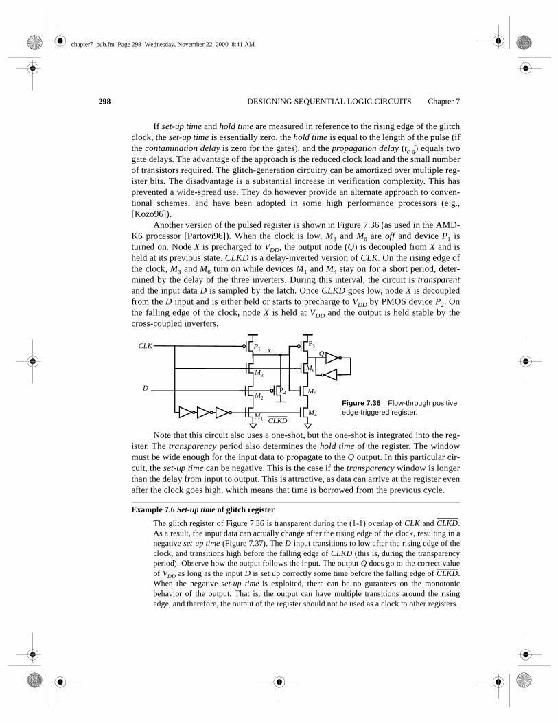
Another version of the pulsed register is shown in Figure 7.36 (as used in the AMD-K6 processor [Partovi96]). When the clock is low, M3 and M6 are off and device P1 isturned on. Node X is precharged to VDD, the output node (Q) is decoupled from X and isheld at its previous state. CLKD is a delay-inverted version of CLK. On the rising edge ofthe clock, M3 and M6 turn on while devices M1 and M4 stay on for a short period, deter-mined by the delay of the three inverters. During this interval, the circuit is transparentand the input data D is sampled by the latch. Once CLKD goes low, node X is decoupledfrom the D input and is either held or starts to precharge to VDD by PMOS device P2. Onthe falling edge of the clock, node X is held at VDD and the output is held stable by thecross-coupled inverters.
Note that this circuit also uses a one-shot, but the one-shot is integrated into the reg-ister. The transparency period also determines the hold time of the register. The windowmust be wide enough for the input data to propagate to the Q output. In this particular cir-cuit, the set-up time can be negative. This is the case if the transparency window is longerthan the delay from input to output. This is attractive, as data can arrive at the register evenafter the clock goes high, which means that time is borrowed from the previous cycle.
Example 7.6 Set-up time of glitch register
The glitch register of Figure 7.36 is transparent during the (1-1) overlap of CLK and CLKD.As a result, the input data can actually change after the rising edge of the clock, resulting in anegative set-up time (Figure 7.37). The D-input transitions to low after the rising edge of theclock, and transitions high before the falling edge of CLKD (this is, during the transparencyperiod). Observe how the output follows the input. The output Q does go to the correct valueof VDD as long as the input D is set up correctly some time before the falling edge of CLKD.When the negative set-up time is exploited, there can be no gurantees on the monotonicbehavior of the output. That is, the output can have multiple transitions around the risingedge, and therefore, the output of the register should not be used as a clock to other registers.
CLK
M1
M2
M3
P1
M4
M5
M6
P3
P2
CLKD
Q
D
Figure 7.36 Flow-through positiveedge-triggered register.
x
chapter7_pub.fm Page 298 Wednesday, November 22, 2000 8:41 AM

Section 7.7 Sense-Amplifier Based Registers 299
Problem 7.7 Converting a glitch register to a conditional glitch register
Modify the circuit in Figure 7.36 so that it takes an additional Enable input. The goal is toconvert the register to a conditional register which latches only when the enable signal isasserted.
7.7 Sense-Amplifier Based Registers
So far, we have presented two fundamental approaches towards building edge-triggeredregisters: the master-slave concept and the glitch technique. Figure 7.38 introducesanother technique that uses a sense amplifier structure to implement an edge-triggeredregister [Montanaro96]. Sense amplifier circuits accept small input signals and amplifythem to generate rail-to-rail swings. As we will see, sense amplifier circuits are usedextensively in memory cores and in low swing bus drivers to amplify small voltage swings
0.0 0.2 0.4 0.6 0.8 1.0time (nsec)
-0.5
0.0
0.5
1.0
1.5
2.0
2.5
3.0
Vol
tsD Q
CLKDCLKFigure 7.37 Simulation showing anegative set-up time for the glitchregister.
VDD
ININ
CLK
OUT OUT
VDD
L1 L2
L4L3
VDD
Figure 7.38 Positive edge-triggeredregister based on sense-amplifier.
M1
M2 M3
M4
M5 M6
M9 M7 M8 M10
chapter7_pub.fm Page 299 Wednesday, November 22, 2000 8:41 AM

300 DESIGNING SEQUENTIAL LOGIC CIRCUITS Chapter 7
present in heavily loaded wires. There are many techniques to construct these amplifiers,with the use of feedback (e.g., cross-coupled inverters) being one common approach. Thecircuit shown in Figure 7.38 uses a precharged front-end amplifier that samples the differ-ential input signal on the rising edge of the clock signal. The outputs of front-end are fedinto a NAND cross-coupled SR FF that holds the data and gurantees that the differentialoutputs switch only once per clock cycle. The differential inputs in this implementationdon’t have to have rail-to-rail swing and hence this register can be used as a receiver for areduced swing differential bus.
The core of the front-end consists of a cross-coupled inverter (M5-M8) whose out-puts (L1 and L2) are precharged using devices M9 and M10 during the low phase of theclock. As a result, PMOS transistors M7 and M8 to be turned off and the NAND FF isholding its previous state. Transistor M1 is similar to an evaluate switch in dynamic cir-cuits and is turned off ensuring that the differential inputs don’t affect the output during thelow phase of the clock. On the rising edge of the clock, the evaluate transistor turns on andthe differential input pair (M2 and M3) is enabled, and the difference between the input sig-nals is amplified on the output nodes on L1 and L2. The cross-coupled inverter pair flips toone of its the stable states based on the value of the inputs. For example, if IN is 1, L1 ispulled to 0, and L2 remains at VDD. Due to the amplifying properties of the input stage, it isnot necessary for the input to swing all the way up to VDD and enables the use of low-swing signaling on the input wires.
The shorting transistor, M4, is used to provide a DC leakage path from either nodeL3, or L4, to ground. This is necessary to accommodate the case where the inputs changetheir value after the positive edge of CLK has occurred, resulting in either L3 or L4 beingleft in a high-impedance state with a logical low voltage level stored on the node. Withoutthe leakage path that node would be susceptible to charging by leakage currents. The latch
Inputs Change (CLK still high)
IN IN0 11 0
0
01
L1L2
L3 L4
highimpedance
IN IN0 11 0
1 00 0
0 01 1
L1L2
L3 L4
IN IN0 11 0
00 1
0 11 0
L1L2
L3 L4
1 0
Initially
L3 is isolated so charge accumu-lates until L1/L3 change state,causing L2 to change state as well.As a result the flip-flop outputs change.
The leakage current attempts tocharge L1/L3 but the DC paththrough the shorting transistorallows it to leak away to ground.
w/o shortingdevice
w/shortingdevice
leakage path leakage path
Figure 7.39 The need for the shorting transistor M4.
chapter7_pub.fm Page 300 Wednesday, November 22, 2000 8:41 AM
Section 7.8 Pipelining: An approach to optimize sequential circuits 301
could then actually change state prior to the next rising edge of CLK! This is best illus-trated graphically, as shown in Figure 7.39.
7.8 Pipelining: An approach to optimize sequential circuits
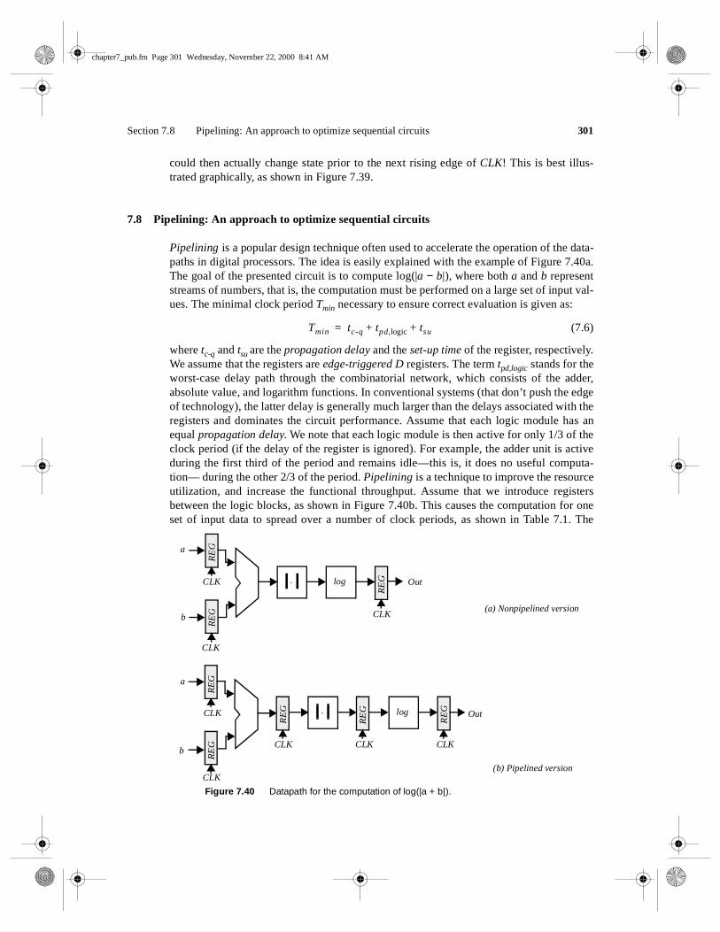
Pipelining is a popular design technique often used to accelerate the operation of the data-paths in digital processors. The idea is easily explained with the example of Figure 7.40a.The goal of the presented circuit is to compute log(|a − b|), where both a and b representstreams of numbers, that is, the computation must be performed on a large set of input val-ues. The minimal clock period Tmin necessary to ensure correct evaluation is given as:
(7.6)
where tc-q and tsu are the propagation delay and the set-up time of the register, respectively.We assume that the registers are edge-triggered D registers. The term tpd,logic stands for theworst-case delay path through the combinatorial network, which consists of the adder,absolute value, and logarithm functions. In conventional systems (that don’t push the edgeof technology), the latter delay is generally much larger than the delays associated with theregisters and dominates the circuit performance. Assume that each logic module has anequal propagation delay. We note that each logic module is then active for only 1/3 of theclock period (if the delay of the register is ignored). For example, the adder unit is activeduring the first third of the period and remains idle—this is, it does no useful computa-tion— during the other 2/3 of the period. Pipelining is a technique to improve the resourceutilization, and increase the functional throughput. Assume that we introduce registersbetween the logic blocks, as shown in Figure 7.40b. This causes the computation for oneset of input data to spread over a number of clock periods, as shown in Table 7.1. The
Figure 7.40 Datapath for the computation of log(|a + b|).
RE
G
CLK
RE
G
CLK
RE
G
CLK
log.
RE
G
CLK
RE
G
CLK
RE
G
CLK
.
RE
G
CLK
RE
G
CLK
log
Out
Out
a
b
a
b
(a) Nonpipelined version
(b) Pipelined version
Tmin tc-q tpd,logic tsu+ +=
chapter7_pub.fm Page 301 Wednesday, November 22, 2000 8:41 AM

302 DESIGNING SEQUENTIAL LOGIC CIRCUITS Chapter 7
result for the data set (a1, b1) only appears at the output after three clock-periods. At thattime, the circuit has already performed parts of the computations for the next data sets, (a2,b2) and (a3,b3). The computation is performed in an assembly-line fashion, hence the namepipeline.
The advantage of pipelined operation becomes apparent when examining the mini-mum clock period of the modified circuit. The combinational circuit block has been parti-tioned into three sections, each of which has a smaller propagation delay than the originalfunction. This effectively reduces the value of the minimum allowable clock period:
(7.7)
Suppose that all logic blocks have approximately the same propagation delay, andthat the register overhead is small with respect to the logic delays. The pipelined networkoutperforms the original circuit by a factor of three under these assumptions, or T min,pipe=Tmin/3. The increased performance comes at the relatively small cost of two additional reg-isters, and an increased latency.1 This explains why pipelining is popular in the implemen-tation of very high-performance datapaths.
7.8.1 Latch- vs. Register-Based Pipelines
Pipelined circuits can be constructed using level-sensitive latches instead of edge-trig-gered registers. Consider the pipelined circuit of Figure 7.41. The pipeline system isimplemented based on pass-transistor-based positive and negative latches instead of edge-triggered registers. That is, logic is introduced between the master and slave latches of amaster-slave system. In the following discussion, we use without loss of generality theCLK-CLK notation to denote a two-phase clock system. Latch-based systems give signifi-cantly more flexibility in implementing a pipelined system, and often offers higher perfor-mance. When the clocks CLK and CLK are nonoverlapping, correct pipeline operation isobtained. Input data is sampled on C1 at the negative edge of CLK and the computation oflogic block F starts; the result of the logic block F is stored on C2 on the falling edge ofCLK, and the computation of logic block G starts. The nonoverlapping of the clocks
Table 7.1 Example of pipelined computations.
Clock Period Adder Absolute Value Logarithm
1 a1 + b1
2 a2 + b2 |a1 + b1|
3 a3 + b3 |a2 + b2| log(|a1 + b1|)
4 a4 + b4 |a3 + b3| log(|a2 + b2|)
5 a5 + b5 |a4 + b4| log(|a3 + b3|)
1 Latency is defined here as the number of clock cycles it takes for the data to propagate from the input tothe output. For the example at hand, pipelining increases the latency from 1 to 3. An increased latency is in gen-eral acceptable, but can cause a global performance degradation if not treated with care.
Tmin ,pipe tc-q max tpd ,add tpd ,abs tpd ,log,( , )+=
chapter7_pub.fm Page 302 Wednesday, November 22, 2000 8:41 AM

Section 7.8 Pipelining: An approach to optimize sequential circuits 303
ensures correct operation. The value stored on C2 at the end of the CLK low phase is theresult of passing the previous input (stored on the falling edge of CLK on C1) through thelogic function F. When overlap exists between CLK and CLK, the next input is alreadybeing applied to F, and its effect might propagate to C2 before CLK goes low (assumingthat the contamination delay of F is small). In other words, a race develops between theprevious input and the current one. Which value wins depends upon the logic function F,the overlap time, and the value of the inputs since the propagation delay is often a func-tion of the applied inputs. The latter factor makes the detection and elimination of raceconditions non-trivial.
7.8.2 NORA-CMOS—A Logic Style for Pipelined Structures
The latch-based pipeline circuit can also be implemented using C2MOS latches, as shownin Figure 7.42. The operation is similar to the one discussed above. This topology has oneadditional, important property:
A C2MOS-based pipelined circuit is race-free as long as all the logic functions F (imple-mented using static logic) between the latches are noninverting.
The reasoning for the above argument is similar to the argument made in the con-struction of a C2MOS register. During a (0-0) overlap between CLK and CLK, all C2MOSlatches, simplify to pure pull-up networks (see Figure 7.27). The only way a signal canrace from stage to stage under this condition is when the logic function F is inverting, asillustrated in Figure 7.43, where F is replaced by a single, static CMOS inverter. Similarconsiderations are valid for the (1-1) overlap.
Based on this concept, a logic circuit style called NORA-CMOS was conceived[Goncalves83]. It combines C2MOS pipeline registers and NORA dynamic logic functionblocks. Each module consists of a block of combinational logic that can be a mixture ofstatic and dynamic logic, followed by a C2MOS latch. Logic and latch are clocked in sucha way that both are simultaneously in either evaluation, or hold (precharge) mode. A block
Figure 7.41 Operation of two-phasepipelined circuit using dynamic registers.
CLK
InF G
Out
C1 C2 C3
compute GCompute F
CLK CLK
CLK
CLK
chapter7_pub.fm Page 303 Wednesday, November 22, 2000 8:41 AM

304 DESIGNING SEQUENTIAL LOGIC CIRCUITS Chapter 7
that is in evaluation during CLK = 1 is called a CLK-module, while the inverse is called aCLK-module. Examples of both classes are shown in Figure 7.44 a and b, respectively.The operation modes of the modules are summarized in Table 7.2.
A NORA datapath consists of a chain of alternating CLK and CLK modules. Whileone class of modules is precharging with its output latch in hold mode, preserving the pre-vious output value, the other class is evaluating. Data is passed in a pipelined fashion frommodule to module.
NORA offers designers a wide range of design choices. Dynamic and static logiccan be mixed freely, and both CLKp and CLKn dynamic blocks can be used in cascaded orin pipelined form. With this freedom of design, extra inverter stages, as required inDOMINO-CMOS, are most often avoided.
In order to ensure correct operation, two important rules should always be followed:
Table 7.2 Operation modes for NORA logic modules.
CLK block CLK block
Logic Latch Logic Latch
CLK = 0 Precharge Hold Evaluate Evaluate
CLK = 1 Evaluate Evaluate Precharge Hold
Design Rules
Figure 7.42 Pipelined datapath using C2MOS latches.
InF Out
CLK
CLK
VDD VDD VDD
C2C1
GC3
CLK
CLK
CLK
CLK
0CLK
CLK
VDD
CLK
CLK
VDDVDD
Figure 7.43 Potential race conditionduring (0-0) overlap in C2MOS-baseddesign.
chapter7_pub.fm Page 304 Wednesday, November 22, 2000 8:41 AM
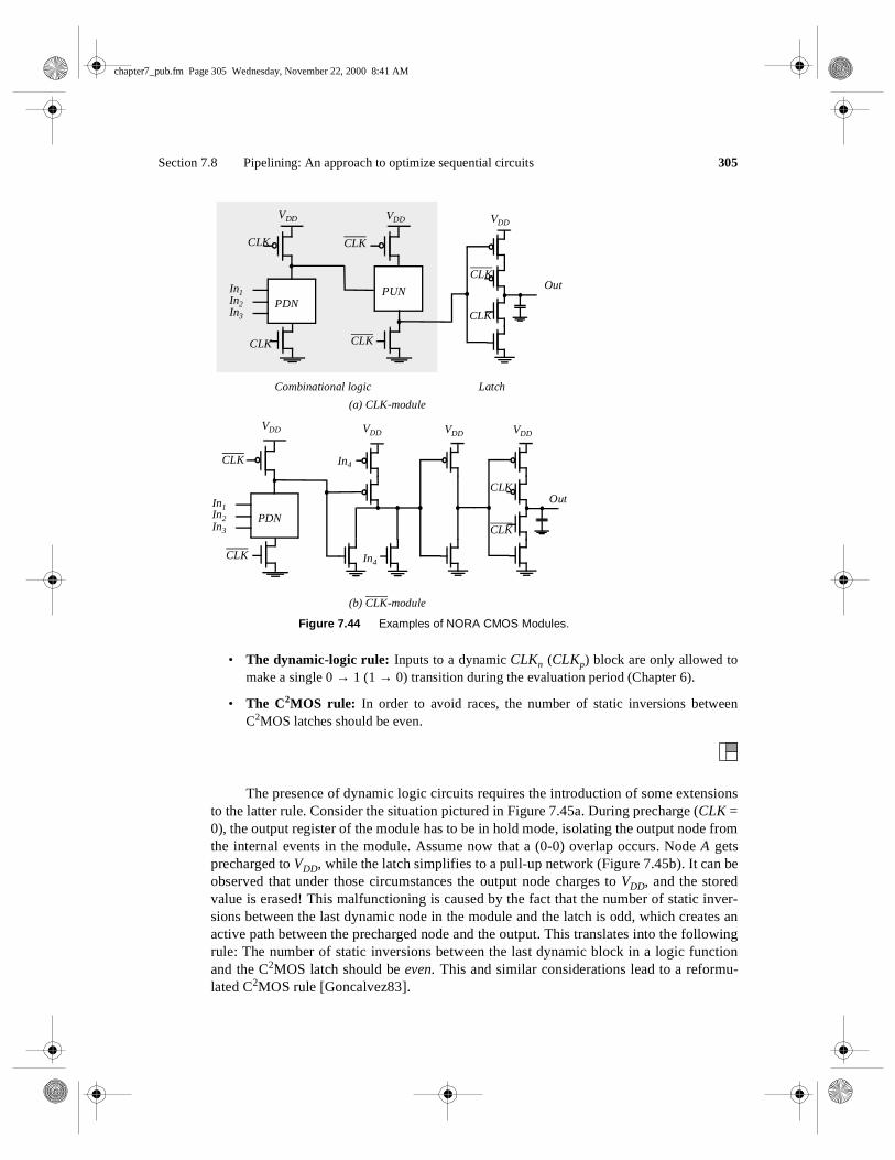
Section 7.8 Pipelining: An approach to optimize sequential circuits 305
• The dynamic-logic rule: Inputs to a dynamic CLKn (CLKp) block are only allowed tomake a single 0 → 1 (1 → 0) transition during the evaluation period (Chapter 6).
• The C2MOS rule: In order to avoid races, the number of static inversions betweenC2MOS latches should be even.
The presence of dynamic logic circuits requires the introduction of some extensionsto the latter rule. Consider the situation pictured in Figure 7.45a. During precharge (CLK =0), the output register of the module has to be in hold mode, isolating the output node fromthe internal events in the module. Assume now that a (0-0) overlap occurs. Node A getsprecharged to VDD, while the latch simplifies to a pull-up network (Figure 7.45b). It can beobserved that under those circumstances the output node charges to VDD, and the storedvalue is erased! This malfunctioning is caused by the fact that the number of static inver-sions between the last dynamic node in the module and the latch is odd, which creates anactive path between the precharged node and the output. This translates into the followingrule: The number of static inversions between the last dynamic block in a logic functionand the C2MOS latch should be even. This and similar considerations lead to a reformu-lated C2MOS rule [Goncalvez83].
Figure 7.44 Examples of NORA CMOS Modules.
CLK
CLK
VDDVDD
PDN
CLK
In1In2In3
CLK
VDD
PUN
CLK
CLK
Out
CLK
CLK
VDD
Out
VDD
PDN
CLK
In1In2In3
CLK
VDD
In4
In4
VDD
(a) CLK-module
(b) CLK-module
Combinational logic Latch
chapter7_pub.fm Page 305 Wednesday, November 22, 2000 8:41 AM

306 DESIGNING SEQUENTIAL LOGIC CIRCUITS Chapter 7
• The number of static inversions between C2MOS latches should be even (in the absenceof dynamic nodes); if dynamic nodes are present, the number of static inverters betweena latch and a dynamic gate in the logic block should be even. The number of static inver-sions between the last dynamic gate in a logic block and the latch should be even as well.
Adhering to the above rules is not always trivial and requires a careful analysis ofthe logic equations to be implemented. This often makes the design of an operationalNORA-CMOS structure cumbersome. Its use should only be considered when maximumcircuit performance is a must.
7.9 Non-Bistable Sequential Circuits
In the preceding sections, we have focused on one single type of sequential element, this isthe latch (and its sibling the register). The most important property of such a circuit is thatit has two stable states, and is hence called bistable. The bistable element is not the onlysequential circuit of interest. Other regenerative circuits can be catalogued as astable andmonostable. The former act as oscillators and can, for instance, be used for on-chip clockgeneration. The latter serve as pulse generators, also called one-shot circuits. Anotherinteresting regenerative circuit is the Schmitt trigger. This component has the useful prop-erty of showing hysteresis in its dc characteristics—its switching threshold is variable anddepends upon the direction of the transition (low-to-high or high-to-low). This peculiarfeature can come in handy in noisy environments.
Revised C2MOS Rule
Figure 7.45 Extended C2MOS rules.
CLK
CLK
VDD
Out
VDD
PDN
CLK
In1
In2
CLK
VDD
A
CLK
CLK
VDD
Out
VDD
PDN
CLK
In1
In2
CLK
VDD
A
(b) Same circuit during (0-0) clock overlap.(a) Circuit with odd number of static inversionsbetween dynamic logic stage and register
chapter7_pub.fm Page 306 Wednesday, November 22, 2000 8:41 AM

Section 7.9 Non-Bistable Sequential Circuits 307
7.9.1 The Schmitt Trigger
Definition
A Schmitt trigger [Schmitt38] is a device with two important properties:
1. It responds to a slowly changing input waveform with a fast transition time at theoutput.
2. The voltage-transfer characteristic of the device displays different switching thresh-olds for positive- and negative-going input signals. This is demonstrated in Figure7.46, where a typical voltage-transfer characteristic of the Schmitt trigger is shown(and its schematics symbol). The switching thresholds for the low-to-high and high-to-low transitions are called VM+ and VM−, respectively. The hysteresis voltage isdefined as the difference between the two.
One of the main uses of the Schmitt trigger is to turn a noisy or slowly varying inputsignal into a clean digital output signal. This is illustrated in Figure 7.47. Notice how thehysteresis suppresses the ringing on the signal. At the same time, the fast low-to-high (andhigh-to-low) transitions of the output signal should be observed. For instance, steep signalslopes are beneficial in reducing power consumption by suppressing direct-path currents.The “secret” behind the Schmitt trigger concept is the use of positive feedback.
Figure 7.46 Non-inverting Schmitt trigger.
In Out
(b) Schematic symbol
Vin
Vout VOH
VOL
VM– VM+
(a) Voltage-transfer characteristic
Figure 7.47 Noise suppression using a Schmitt trigger.
VM+
VM–
VoutVin
t tt0 t0 + tp
chapter7_pub.fm Page 307 Wednesday, November 22, 2000 8:41 AM

308 DESIGNING SEQUENTIAL LOGIC CIRCUITS Chapter 7
CMOS Implementation
One possible CMOS implementation of the Schmitt trigger is shown in Figure 7.48. Theidea behind this circuit is that the switching threshold of a CMOS inverter is determinedby the (kn/kp) ratio between the NMOS and PMOS transistors. Increasing the ratio resultsin a reduction of the threshold, while decreasing it results in an increase in VM. Adaptingthe ratio depending upon the direction of the transition results in a shift in the switchingthreshold and a hysteresis effect. This adaptation is achieved with the aid of feedback.
Suppose that Vin is initially equal to 0, so that Vout = 0 as well. The feedback loopbiases the PMOS transistor M4 in the conductive mode while M3 is off. The input signaleffectively connects to an inverter consisting of two PMOS transistors in parallel (M2 andM4) as a pull-up network, and a single NMOS transistor (M1) in the pull-down chain. Thismodifies the effective transistor ratio of the inverter to kM1/(kM2+kM4), which moves theswitching threshold upwards.
Once the inverter switches, the feedback loop turns off M4, and the NMOS deviceM3 is activated. This extra pull-down device speeds up the transition and produces a cleanoutput signal with steep slopes.
A similar behavior can be observed for the high-to-low transition. In this case, thepull-down network originally consists of M1 and M3 in parallel, while the pull-up networkis formed by M2. This reduces the value of the switching threshold to VM–.
Example 7.7 CMOS Schmitt Trigger
Consider the schmitt trigger with the following device sizes. Devices M1 and M2 are1µm/0.25µm, and 3µm/0.25µm, respectively. The inverter is sized such that the switchingthreshold is around VDD/2 (= 1.25 V). Figure 7.49a shows the simulation of the Schmitt trig-ger assuming that devices M3 and M4 are 0.5µm/0.25µm and 1.5µm/0.25µm, respectively. Asapparent from the plot, the circuit exhibits hysteresis. The high-to-low switching point (VM- =0.9 V) is lower than VDD/2, while the low-to-high switching threshold (VM+ = 1.6 V) is largerthan VDD/2.
It is possible to shift the switching point by changing the sizes of M3 and M4. Forexample, to modify the low-to-high transition, we need to vary the PMOS device. The high-to-low threshold is kept constant by keeping the device width of M3 at 0.5 µm. The devicewidth of M4 is varied as k * 0.5µm. Figure 7.49b demonstrates how the switching thresholdincreases with raising values of k.
VDD
Vin Vout
M1
M2
M3
M4
Figure 7.48 CMOS Schmitt trigger.
X
chapter7_pub.fm Page 308 Wednesday, November 22, 2000 8:41 AM

Section 7.9 Non-Bistable Sequential Circuits 309
Problem 7.8 An Alternative CMOS Schmitt Trigger
Another CMOS Schmitt trigger is shown in Figure 7.50. Discuss the operation of the gate,and derive expressions for VM− and VM+.
7.9.2 Monostable Sequential Circuits
A monostable element is a circuit that generates a pulse of a predetermined width everytime the quiescent circuit is triggered by a pulse or transition event. It is called monostablebecause it has only one stable state (the quiescent one). A trigger event, which is either asignal transition or a pulse, causes the circuit to go temporarily into another quasi-stablestate. This means that it eventually returns to its original state after a time period deter-mined by the circuit parameters. This circuit, also called a one-shot, is useful in generatingpulses of a known length. This functionality is required in a wide range of applications.We have already seen the use of a one-shot in the construction of glitch registers. Another
0.0 0.5 1.0 1.5 2.0 2.5
Vin(V)
0.0
0.5
1.0
1.5
2.0
2.5V
X(V
)
Figure 7.49 Schmitt trigger simulations.
VM+
VM-
0.0 0.5 1.0 1.5 2.0 2.5
Vin(V)
0.0
0.5
1.0
1.5
2.0
2.5
Vx
(V)
k=1
k=2
k=3
k=4
(b) The effect of varying the ratio of thePMOS device M4. The width is k * 0.5µm.
(a) Voltage-transfer characteristics with hysteresis.
Figure 7.50 Alternate CMOS Schmitt trigger.
In
VDD
VDD
Out
M1
M2
M3
M4
M5
M6
X
chapter7_pub.fm Page 309 Wednesday, November 22, 2000 8:41 AM

310 DESIGNING SEQUENTIAL LOGIC CIRCUITS Chapter 7
notorious example is the address transition detection (ATD) circuit, used for the timinggeneration in static memories. This circuit detects a change in a signal, or group of signals,such as the address or data bus, and produces a pulse to initialize the subsequent circuitry.
The most common approach to the implementation of one-shots is the use of a sim-ple delay element to control the duration of the pulse. The concept is illustrated in Figure7.51. In the quiescent state, both inputs to the XOR are identical, and the output is low. Atransition on the input causes the XOR inputs to differ temporarily and the output to gohigh. After a delay td (of the delay element), this disruption is removed, and the outputgoes low again. A pulse of length td is created. The delay circuit can be realized in manydifferent ways, such as an RC-network or a chain of basic gates.
7.9.3 Astable Circuits
An astable circuit has no stable states. The output oscillates back and forth between twoquasi-stable states with a period determined by the circuit topology and parameters (delay,power supply, etc.). One of the main applications of oscillators is the on-chip generation ofclock signals. This application is discussed in detail in a later chapter (on timing).
The ring oscillator is a simple, example of an astable circuit. It consists of an oddnumber of inverters connected in a circular chain. Due to the odd number of inversions, nostable operation point exists, and the circuit oscillates with a period equal to 2 × tp × N,with N the number of inverters in the chain and tp the propagation delay of each inverter.
Example 7.8 Ring oscillator
The simulated response of a ring oscillator with five stages is shown in Figure 7.52 (all gatesuse minimum-size devices). The observed oscillation period approximately equals 0.5 nsec,which corresponds to a gate propagation delay of 50 psec. By tapping the chain at variouspoints, different phases of the oscillating waveform are obtained (phases 1, 3, and 5 are dis-
DELAYtd
In
Outtd
Figure 7.51 Transition-triggered one-shot.
Figure 7.52 Simulatedwaveforms of five-stage ringoscillator. The outputs of stages 1,3, and 5 are shown.
v1 v3 v5
0.0 0.5 1.0 1.5time (nsec)
-0.5
0.0
0.5
1.0
1.5
2.0
2.5
3.0
Vol
ts
chapter7_pub.fm Page 310 Wednesday, November 22, 2000 8:41 AM
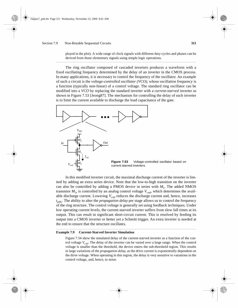
Section 7.9 Non-Bistable Sequential Circuits 311
played in the plot). A wide range of clock signals with different duty-cycles and phases can bederived from those elementary signals using simple logic operations.
The ring oscillator composed of cascaded inverters produces a waveform with afixed oscillating frequency determined by the delay of an inverter in the CMOS process.In many applications, it is necessary to control the frequency of the oscillator. An exampleof such a circuit is the voltage-controlled oscillator (VCO), whose oscillation frequency isa function (typically non-linear) of a control voltage. The standard ring oscillator can bemodified into a VCO by replacing the standard inverter with a current-starved inverter asshown in Figure 7.53 [Jeong87]. The mechanism for controlling the delay of each inverteris to limit the current available to discharge the load capacitance of the gate.
In this modified inverter circuit, the maximal discharge current of the inverter is lim-ited by adding an extra series device. Note that the low-to-high transition on the invertercan also be controlled by adding a PMOS device in series with M2. The added NMOStransistor M3, is controlled by an analog control voltage Vcntl, which determines the avail-able discharge current. Lowering Vcntl reduces the discharge current and, hence, increasestpHL. The ability to alter the propagation delay per stage allows us to control the frequencyof the ring structure. The control voltage is generally set using feedback techniques. Underlow operating current levels, the current-starved inverter suffers from slow fall times at itsoutput. This can result in significant short-circuit current. This is resolved by feeding itsoutput into a CMOS inverter or better yet a Schmitt trigger. An extra inverter is needed atthe end to ensure that the structure oscillates.
Example 7.9 Current-Starved Inverter Simulation
Figure 7.54 show the simulated delay of the current-starved inverter as a function of the con-trol voltage Vcntl. The delay of the inverter can be varied over a large range. When the controlvoltage is smaller than the threshold, the device enters the sub-threshold region. This resultsin large variations of the propagation delay, as the drive current is exponentially dependent onthe drive voltage. When operating in this region, the delay is very sensitive to variations in thecontrol voltage, and, hence, to noise.
Figure 7.53 Voltage-controlled oscillator based oncurrent-starved inverters.
VDD
M3
M1
M2
Iref
OutIn
Vcntl
chapter7_pub.fm Page 311 Wednesday, November 22, 2000 8:41 AM
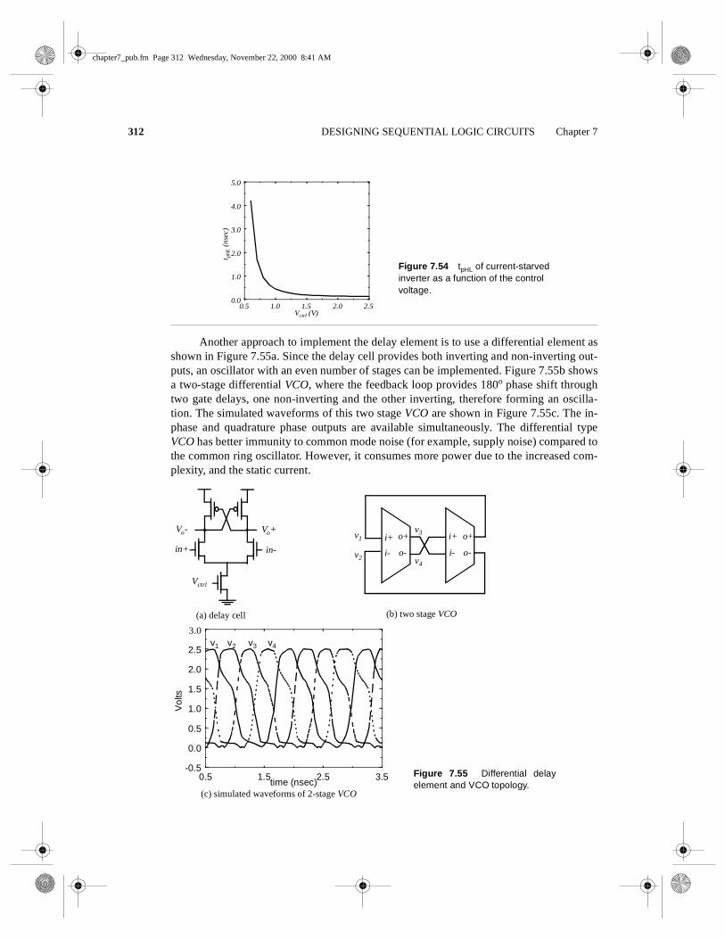
312 DESIGNING SEQUENTIAL LOGIC CIRCUITS Chapter 7
Another approach to implement the delay element is to use a differential element asshown in Figure 7.55a. Since the delay cell provides both inverting and non-inverting out-puts, an oscillator with an even number of stages can be implemented. Figure 7.55b showsa two-stage differential VCO, where the feedback loop provides 180o phase shift throughtwo gate delays, one non-inverting and the other inverting, therefore forming an oscilla-tion. The simulated waveforms of this two stage VCO are shown in Figure 7.55c. The in-phase and quadrature phase outputs are available simultaneously. The differential typeVCO has better immunity to common mode noise (for example, supply noise) compared tothe common ring oscillator. However, it consumes more power due to the increased com-plexity, and the static current.
Figure 7.54 tpHL of current-starvedinverter as a function of the controlvoltage.
0.5 1.0 1.5 2.0 2.5Vctrl (V)
0.0
1.0
2.0
3.0
4.0
5.0
t pH
L(n
sec)
in+ in-
Vo+Vo-
Vctrl
i-
i+ i+
i-
o+
o-
o+
o-
(a) delay cell (b) two stage VCO
v1
v2
v3
v4
Figure 7.55 Differential delayelement and VCO topology.
0.5 1.5 2.5 3.5time (nsec)
-0.5
0.0
0.5
1.0
1.5
2.0
2.5
3.0
Vol
ts
v2 v3 v4v1
(c) simulated waveforms of 2-stage VCO
chapter7_pub.fm Page 312 Wednesday, November 22, 2000 8:41 AM

Section 7.10 Perspective: Choosing a Clocking Strategy 313
7.10 Perspective: Choosing a Clocking Strategy
A crucial decision that must be made in the earliest phases of a chip design is to select theappropriate clocking methodology. The reliable synchronization of the various operationsoccurring in a complex circuit is one of the most intriguing challenges facing the digitaldesigner of the next decade. Choosing the right clocking scheme affects the functionality,speed and power of a circuit.
A number of widely-used clocking schemes were introduced in this chapter. Themost robust and conceptually simple scheme is the two-phase master-slave design. Thepredominant approach is use the multiplexer-based register, and to generate the two clockphases locally by simply inverting the clock. More exotic schemes such as the glitch regis-ter are also used in practice. However, these schemes require significant hand tuning andmust only be used in specific situations. An example of such is the need for a negative set-up time to cope with clock skew.
The general trend in high-performance CMOS VLSI design is therefore to use sim-ple clocking schemes, even at the expense of performance. Most automated design meth-odologies such as standard cell employ a single-phase, edge-triggered approach, based onstatic flip-flops. But the tendency towards simpler clocking approaches is also apparent inhigh-performance designs such as microprocessors. The use of latches between logic isalso very common to improve circuit performance.
7.11 Summary
This chapter has explored the subject of sequential digital circuits. The following topicswere discussed:
• The cross-coupling of two inverters creates a bistable circuit, called a flip-flop. Athird potential operation point turns out to be metastable; that is, any diversion fromthis bias point causes the flip-flop to converge to one of the stable states.
• A latch is a level-sensitive memory element that samples data on one phase andholds data on the other phase. A register (sometime also called a flip-flop) on theother hand samples the data on the rising or falling edge. A register has three impor-tant parameter the set-up time, the hold time, and the propagation delay. Theseparameters must be carefully optimized since they may account for a significantportion of the clock period.
• Registers can be static or dynamic. A static register holds state as long as the powersupply is turned on. It is ideal for memory that is accessed infrequently (e.g., recon-figuration registers or control information). Dynamic memory is based on temporarycharge store on capacitors. The primary advantage is the reduced complexity andhigher performance/lower power. However, charge on a dynamic node leaks awaywith time, and hence dynamic circuits have a minimum clock frequency.
• There are several fundamentally different approaches towards building a register.The most common and widely used approach is the master-slave configurationwhich involves cascading a positive latch and negative latch (or vice-versa).
chapter7_pub.fm Page 313 Wednesday, November 22, 2000 8:41 AM

314 DESIGNING SEQUENTIAL LOGIC CIRCUITS Chapter 7
• Registers can also be constructed using the pulse or glitch concept. An intentionalpulse (using a one shot circuit) is used to sample the input around an edge. Gener-ally, the design of such circuits requires careful timing analysis across all processcorners. Sense-amplifier based schemes are also used to construct registers and areto be used when high performance or low signal swing signalling is required.
• Choice of clocking style is an important consideration. Two phase design can resultin race problems. Circuit techniques such as C2MOS can be used to eliminate raceconditions in two-phase clocking. Another option is to use true single phase clock-ing. However, the rise time of clocks must be carefully optimized to eliminate races.
• The combination of dynamic logic with dynamic latches can produce extremely fastcomputational structures. An example of such an approach, the NORA logic style, isvery effective in pipelined datapaths.
• Monostable structures have only one stable state. They are useful as pulse generators.
• Astable multivibrators, or oscillators, possess no stable state. The ring oscillator isthe best-known example of a circuit of this class.
• Schmitt triggers display hysteresis in their dc characteristic and fast transitions intheir transient response. They are mainly used to suppress noise.
7.12 To Probe Further
The basic concepts of sequential gates can be found in many logic design textbooks (e.g.,[Mano82] and [Hill74]). The design of sequential circuits is amply documented in most ofthe traditional digital circuit handbooks.
References
[Dopperpuhl92] D. Dopperpuhl et al., “A 200 MHz 64-b Dual Issue CMOS Microprocessor,” IEEEJSSC, vol. 27, no. 11, Nov. 1992, pp. 1555–1567.
[Gieseke97] B. Bieseke et al., “A 600MHz Superscalar RISC Microprocessor with Out-Of-OrderExecution,” IEEE ISSCC, pp. 176-177, Feb. 1997.
[Goncalves83] N. Goncalves and H. De Man, “NORA: a racefree dynamic CMOS technique forpipelined logic structures,” IEEE JSSC, vol. SC-18, no. 3, June 1983, pp. 261–266.
[Haznedar91] H. Haznedar, Digital Microelectronics, Benjamin/Cummings, 1991.
[Hill74] F. Hill and G. Peterson, Introduction to Switching Theory and Logical Design, Wiley, 1974.
[Hodges88] D. Hodges and H. Jackson, Analysis and Design of Digital Integrated Circuits,McGraw-Hill, 1988.
[Jeong87] D. Jeong et al., “Design of PLL-based clock generation circuits,” IEEE JSSC, vol. SC-22,no. 2, April 1987, pp. 255–261.
[Kuzo96] S. Kuzo et al., “A 100MHz 0.4W RISC Processor with 200MHz Multiply-Adder, usingPulse-Register Technique,” IEEE ISSCC, pp. 140-141, February 1996.
[Mano82] M. Mano, Computer System Architecture, Prentice Hall, 1982.
[Montanaro96] J. Montanaro et al., “A 160-MHz, 32-b, 0.5-W CMOS RISC Microprocessor,” IEEEJSSC, pp. 1703-1714, November 1996.
chapter7_pub.fm Page 314 Wednesday, November 22, 2000 8:41 AM

Section 7.12 To Probe Further 315
[Mutoh95] S. Mutoh et al., “1-V Power Supply High-Speed Digital Circuit Technology with Multi-threshold-Voltage CMOS,” IEEE JSSC , pp. 847-854, August 1995.
[Partovi96] H. Partovi, “Flow-Through Latch and Edge-Triggered Flip Flop Hybrid Elements,”IEEE ISSCC, pp. 138-139, February 1996.
[Schmitt38] O. H. Schmitt, “A Thermionic Trigger,” Journal of Scientific Instruments, vol. 15, Jan-uary 1938, pp. 24–26.
[Shoji88] M. Shoji, CMOS Digital Circuit Technology, Prentice Hall, 1988.
[Suzuki73] Y. Suzuki, K. Odagawa, and T. Abe, “Clocked CMOS calculator circuitry,” IEEE Jour-nal of Solid State Circuits, vol. SC-8, December 1973, pp. 462–469.
[Veendrick92] H. Veendrick, MOS ICs: From Basics to ASICs, VCH, Weinheim, 1992.
[Yuan89] J. Yuan and Svensson C., “High-Speed CMOS Circuit Technique,” IEEE JSSC, vol. 24,no. 1, February 1989, pp. 62–70.
chapter7_pub.fm Page 315 Wednesday, November 22, 2000 8:41 AM
Top Related