


Languages
Pages
Legal


Design of a Modified Cherry-Hooper Transimpedance Amplifier with DC Offset
Cancellation
by
Kyle LaFevre
A Thesis Presented in Partial Fulfillment
of the Requirements for the Degree
Master of Science
Approved July 2011 by the
Graduate Supervisory Committee:
Bertan Bakkaloglu, Chair
Bert Vermeire
Hugh Barnaby
ARIZONA STATE UNIVERSITY
August 2011
i
ABSTRACT
Optical receivers have many different uses covering simple infrared
receivers, high speed fiber optic communication and light based instrumentation.
All of them have an optical receiver that converts photons to current followed by
a transimpedance amplifier to convert the current to a useful voltage. Different
systems create different requirements for each receiver. High speed digital
communication require high throughput with enough sensitivity to keep the bit
error rate low. Instrumentation receivers have a lower bandwidth, but higher gain
and sensitivity requirements.
In this thesis an optical receiver for use in instrumentation in presented. It
is an entirely monolithic design with the photodiodes on the same substrate as the
CMOS circuitry. This allows for it to be built into a focal-plane array, but it
places some restriction on the area. It is also designed for in-situ testing and must
be able to cancel any low frequency noise caused by ambient light. The area
restrictions prohibit the use of a DC blocking capacitor to reject the low frequency
noise. In place a servo loop was wrapped around the system to reject any DC
offset.
A modified Cherry-Hooper architecture was used for the transimpedance
amplifier. This provides the flexibility to create an amplifier with high gain and
wide bandwidth that is independent of the input capacitance. The downside is the
increased complexity of the design makes stability paramount to the design.
Another drawback is the high noise associated with low input impedance that
decouples the input capacitance from the bandwidth. This problem is
ii
compounded by the servo loop feed which leaves the output noise of some
amplifiers directly referred to the input. An in depth analysis of each circuit
block's noise contribution is presented.
iii
Dedicated to my family.

iv
ACKNOWLEDGMENTS
I would like to thank my advisor Dr. Bertan Bakkaloglu for his support
throughout this project. He has been an inspiration for me to attain the breadth of
knowledge he posses’ and share it in the same jovial manner he does. I would also
like to thank Dr. Bert Vermaire for his support and ability to shield me from the
mess of acquiring funding for this work. Dr. Hugh Barnaby was also
tremendously helpful with this work. I want to thank him for answering any
question I brought to him and coordinating my work with some of my peers.
I would also like to thank my family for always supporting me while I
have pursued my education. I am particularly thankful for my wonderful wife
who agreed to follow me into the desert while I pursue a higher education.
v
TABLE OF CONTENTS
CHAPTER 1: INTRODUCTION Page
1.1 TIA Uses and Overview 1
1.2 Thesis Structure 3
CHAPTER 2: CONVENTIONAL TIA DESIGN 4
2.1 Optical Receiver Basics 4
2.2 Basics of a Transimpedance Amplifier 6
2.3 Primitive Transimpedance Amplifier 7
2.4 Shunt-Shunt Transimpedance Amplifier 8
2.5 Common Gate Transimpedance Amplifier 10
2.6 Regulated Gate Cascode 13
2.7 Cherry-Hooper Design 15
2.8 Modified Cherry-Hooper Design 18
2.9 Modified Cherry Hooper Design as a TIA 21
2.10 Literature Review 24
CHAPTER 3: IMPLEMENTATION OF A BANDPASS TIA 26
3.1 Servo Loop Design 26
3.2 Circuit Overview 27
3.3 Design Specifications 29
3.4 Modified Cherry-Hooper TIA 29
3.5 Op-Amp Design 32
3.6 Integrator Design 33
3.7 OTA Design 34
vi
CHAPTER 4: SIMULATION RESULTS Page
4.1 TIA Characterization 37
4.2 Characterization of the LPF 39
4.3 Characterization of the Integrator 41
4.4 Characterization of the OTA 43
4.5 Characterization of the Complete Circuit 44
4.6 Conclusion 49

vii
LIST OF FIGURES
Figure Page
1 A block diagram of a general photodiode receiver circuit 1
2 Input referred noise 6
3 Photodiode with load resistance 7
4 Photodiode and resistor with noise sources 8
5 Model of transresistance amplifier 9
6 Common gate architecture 11
7 Common gate amplifier with major noise sources shown 13
8 Input of regulated gate cascode amplifier 14
9 The basic Cherry-Hooper topology 15
10 Schematic of a Cherry-Hooper amplifier 17
11 Modified Cherry-Hooper topology 18
12 A schematic of a modified CH amplifier 20
13 A modified CH TIA with a common gate input stage 22
14 Schematic of a modified CH TIA 23
15 A block diagram of a voltage amplifier with a servo loop 26
16 Block diagram of the presented design 28
17 Schematic of the presented TIA 31
18 Schematic of the opamp used in the LPF 32
19 Schematic of the amplifier used in the integrator 33
20 Schematic of the transconductance amplifier used 35
21 Test bench for the TIA 37

viii
Figure Page
22 Gain and bandwidth of the TIA 38
23 Input referred noise of the TIA 38
24 Third order intermodulated distortion of the TIA 39
25 Gain and bandwidth of the LPF 40
26 Input referred noise at the Tia caused by the LPF 41
27 Gain and bandwidth of the integrator 42
28 The spectral density of the integrator noise referred to the TIA input 42
29 The spectral density of the OTA noise referred to the input of the TIA 43
30 Gain and bandwidth of the complete circuit 44
31 Transient simulation of the input current showing DC offset cancellation
and stability 45
32 Superposition of all noise sources compared to total input referred noise 45
33 The intermodulated distortion of the complete circuit 46
34 Transient output simulation 47
35 Transient simulation with slowing rising DC offset of 0A to 40µA 47
36 Transient simulation showing input DC offset and feedback current
through the OTA 48

ix
LIST OF TABLES
Table Page
1 Design specifications for TIA 5
2 Comparison of state of the art TIAs 24
3 List of equations that define the presented circuits parameters 28
4 Design specifications of the TIA 29
5 Transistor sizes used in the TIA 31
6 Resistor values for the TIA schematic 32
x
PREFACE
The design of an optical receiver, like most electronics design, is full of
tradeoffs. This study delves into the design of a monolithic photodiode and
transimpedance amplifier for use in an instrumentation system such as a laser
vibrometer. For the transimpedance amplifier a modified Cherry-Hooper topology
was used. One of the primary challenges for this type of receiver is low frequency
noise caused by ambient light and the laser itself. A servo loop was implemented
to cancel out any low frequency noise or DC input offset.
Chapter 1 introduces the concept of a transimpedance amplifier. An
explanation of why this circuit is useful is shown along with some critical design
parameters.
Chapter 2 covers conventional TIA design. An analysis of the different
stages used in the presented Cherry-Hooper design was made. The advantages and
drawbacks of the different design are highlighted with a focus on low noise
design.
Chapter 3 describes how the servo loop cancels any input DC offset while
providing the design details of the entire system. The transistor level design and
bias conditions for each stage is provided with an explanation of how each portion
impacts the entire design.
Chapter 4 presents the simulation results for the entire design. A
juxtaposition of predicted performance and simulated results is provided. The
device was manufactured, but budget and time constraints prohibited the results

xi
from being available for this paper. The characterization will be included with the
following doctoral dissertation.
1
CHAPTER 1 INTRODUCTION
1.1 TIA USES AND OVERVIEW
Optical receivers are a common occurrence in everyday life. They may be
a small part of a system, like the infrared receiver on a television, or a very
complex system as part of a modern high speed fiber optic communication
scheme. What every receiver has in common is they all use a photodiode to
convert photons to current and a transimpedance amplifier to convert the current
to a useful output voltage. This paper is focused on a monolithic optical receiver
for use in a laser vibrometer system.
Many different laser vibrometers already exist, but they all large and only
suited for use inside of a laboratory. Creating an optical receiver specifically for a
laser vibrometer is a step to allow the entire system to be miniaturized and made
portable. As shown in (14) a scanning laser vibrometer system is very useful for
shallow underground imaging. Ground penetrating radar has been extensively
used for underground imaging, but has many drawbacks a laser vibrometer system
can address. The most important improvements with the laser vibrometer are its
ability to detect nonmetal objects, work in any soil type and detect objects that are
less than 30cm deep.
Designing an optical receiver for a laser vibrometer provides some unique
challenges. A very high resolution ADC will be used so the noise of the system
must be less than an LSB of the ADC. Also the amplifier will be used in-situ and

2
so it must be able to ignore any unwanted signals. These unwanted signals include
ambient light, noise from the laser source and anything else.
A Sample/Hold ADC
Photodiode
R
Digital Out
TIA
Fig. 1 A block diagram of a general photodiode receiver circuit
The focus of this paper is the transimpedance amplifier. Current research
in TIA design is focused on high speed digital communication. These receivers
typically have less gain with a wider bandwidth. They are often single ended
receivers employing inductive peaking to try and get the bandwidth as wide as
possible with current technology. Often, they are characterized using eye
diagrams and bit error rate. The amplifier proposed here is a high gain, lower
bandwidth design for analog purposes. Linearity over a range of frequencies is
important so the amplifier is characterized by its gain, bandwidth, input referred
noise, and harmonic distortion.
The TIA was implemented using a Cherry-Hooper topology. This
topology has a low input impedance which allows for a large photodiode with a
large parasitic capacitance, but it would also requires the input to be DC coupled
since a DC blocking capacitor has to be very large. The gain and bandwidth are
also independently tunable to achieve a high gain with a wide bandwidth. The
drawbacks to this design is the output dynamic range is limited and the input is
DC coupled.

3
Since the design must be DC coupled any input offset has to potential to
saturate the amplifier. A servo loop was used to keep the amplifier from saturating
by cancelling out any input offset. The design is required to cancel out a DC
offset that is up to ten times larger than the signal of interest. The servo loop
works by shunting any DC or low frequency current to ground to keep it from
entering the amplifier.
1.2 THESIS STRUCTURE
CHAPTER 2 describes the different methods of characterizing a TIA, how
they are measured and what they mean. A block by block analysis of the system is
then described, with each blocks characterization and implications of those
measurements on the system. CHAPTER 3 covers the actual design that was
manufactured and all of the simulation results are also presented. CHAPTER 4
concludes this paper with the test plan, measurement setup and measurement
results.

4
CHAPTER 2 CONVENTIONAL TIA DESIGN
2.1 OPTICAL RECEIVER BASICS
The basis of an optical receiver is the photodiode and significant research
is going in to making them more useful in optical receivers. A photodiode works
by converting an incident optical signal into an electrical current. It is a square
law device where the electrical current depends on the power of the incident
optical signal. The TIA typically has a linear output voltage that is followed by
either a high gain limiting amplifier (LA) or analog to digital converter (ADC)
depending how the signal is to be used.
High gain LAs are used to convert the relatively small signal TIA output
to a full scale rail-to-rail output voltage. The LA is a non-linear amplifier with an
output that saturates for very small input signals. The use of this is to generate an
output voltage that is constant over a range of input voltages. This output voltage
is also large enough to be considered a detectable logic level. This can then be
used with a flip-flop and clock recovery circuit to act as a digital receiver.
The focus of this thesis is on the TIA which is commonly referred to as the
analog front end (AFE) of any optical receiver circuit. This circuit was designed
to be followed by analog filters and an ADC which makes the specifications very
different from a digital receiver. It is a very high gain amplifier design to sense a
high frequency small signal that is riding on top of a low frequency signal whose
variation is 10 times greater than the desired signal. Such a large DC input
variation would saturate the amplifier without DC input compensation. A servo

5
loop was wrapped around the amplifier which shunts any low frequency noise to
ground while allowing the higher frequency signal to pass into the amplifier.
2.1.1 RECEIVER SPECIFICATIONS
Digital optical receivers are characterized by sensitivity and achievable bit
rate. Sensitivity is measured as bit error rate (BER). BER is defined as the number
of incorrectly detected bits per total number of bits sent and is typically on the
order of 10-12
. BER is very useful figure of merit since it depends on the gain,
bandwidth, and input referred noise of the amplifier. In a design the required BER
and achievable bit rate entirely define the requirements of the TIA.
For the analog receiver presented here the specifications are different.
Noise requirements are much greater for the analog design while gain and
bandwidth are directly specified. A unique specification to the design is the
amount of dark current it can handle. Dark current is the output current of the
photodiode from ambient light and low frequency noise. The following table
shows the required design specifications. The primary challenges are the low
input referred noise specification and the ability to reject dark current that is 10
times greater than the input signal level.
Table 1: Design specifications for TIA.
Parameter Specification
Transimpedance Gain (ZT) 210kΩ
Input Impedance (CPD) 0.8pF

6
Input Dynamic Range 4nA to 4µA
Output Dynamic Range 1mV to 1V
Input Referred Noise Density 0.35 √ ⁄
Bandwidth 15MHz to 35MHz
Gain Bandwidth Product 6.3THz*Ω
Dark Current 0 to 40µA
2.2 BASICS OF A TRANSIMPEDANCE AMPLIFIER
The purpose of a transimpedance amplifier is to convert the output current
of a photodiode to a useful voltage. The ratio of the output voltage to in the input
current is the transimpedance gain of the amplifier
|
|
(2.21)
Noise of TIA is defined by the input referred noise. Input referred noise is
the current noise that would be added to an equivalent noiseless TIA. Noise
measurement is made by observing the output noise voltage and dividing it down
by the transimpedance gain. Figure 2.1 shows the equivalent noise circuits
defined in equation 2.22
TIA
Iin
VoutTIA
Iin
Vout
Fig. 2: Input referred noise.
𝑣𝑛,𝑜𝑢𝑡2
𝑖𝑛,𝑖𝑛2

7
| , | | , |
| |
(2.22)
2.3 PRIMITIVE TRANSIMPEDANCE AMPLIFIER
The most basic way to create a TIA is to simply use a resistor. This is
shown in figure 3. The current to voltage transformation is well known by Ohm’s
law. The downside to such a simple receiver is the gain, bandwidth, and noise are
dependent on the resistance.
PD
R
Vout
Fig. 3: Photodiode with load resistance.
The transimpedance gain RT is simply equal to RL. The –3dB bandwidth is
simply the RC time constant formed by the load and the parasitic capacitance of
the photodiode, CPD. This implies that increasing the bandwidth of the TIA
requires a reduced gain.
2
(2.31)
The noise of the system is also set by RL. A schematic with noise sources
is shown in figure 4. Since the thermal noise of the resistor is in parallel with the
input current, all of the noise shows up at the input so the input referred noise is

8
equal to the resistor noise. Equation 2.32 shows the input referred noise with kB
being Boltzmann’s constant and T is temperature in Kelvin.
,
(2.32)
PD
R
Vout
Fig. 4: Photodiode and resistor with noise sources.
A more complex design is required in order to decouple the gain,
bandwidth and noise. These circuits allow for the gain and bandwidth to be
independent of the parasitic input capacitance. They also allow for a greater
dynamic range.
2.4 SHUNT-SHUNT TRANSIMPEDANCE AMPLIFLIER
One of the more common TIA topologies is the shunt-shunt amplifier. It is
made up of a voltage amplifier with a shunt feedback resistor as shown in figure
5. The high input impedance of the voltage amp forces all of the input current
through the feedback resistor. This causes the gain of the TIA to be equal to the
feedback resistance assuming the gain of the voltage amplifier is much greater
than one.
𝑖𝑛,𝑅2
9
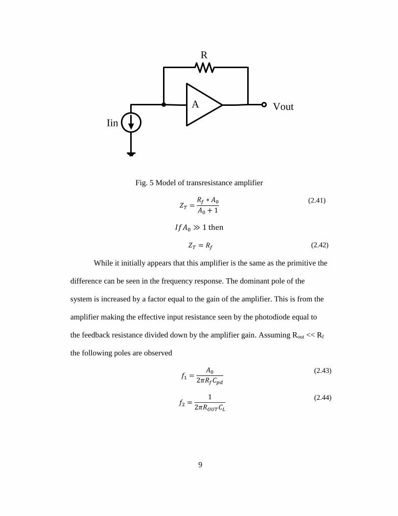
R
A Vout
Iin
Fig. 5 Model of transresistance amplifier
(2.41)
(2.42)
While it initially appears that this amplifier is the same as the primitive the
difference can be seen in the frequency response. The dominant pole of the
system is increased by a factor equal to the gain of the amplifier. This is from the
amplifier making the effective input resistance seen by the photodiode equal to
the feedback resistance divided down by the amplifier gain. Assuming Rout << Rf
the following poles are observed
2
(2.43)
2
(2.44)
10
This amplifier is often treated as a single pole system with f1 the dominant
pole, but if f1 and f2 are close it must be viewed as a 2nd
order system with the
following definition
( ⁄ ) 2 ( ⁄ ) (2.45)
Where
√
(2.46)
2
√( )
(2.47)
With the second order system value of Q must be large for the amplifier to
remain stable. It is possible to achieve a very wide bandwidth and high gain with
a very low Q, but it is unrealistic to expect the amplifier to work. As Q decreases
the phase margin also decreases with a larger amount of ringing and overshoot. A
generally accepted compromise is to set Q equal to 0.7 to provide a good tradeoff
between ringing and stability.
2.5 COMMON GATE TRANSIMPEDANCE AMPLIFIER
A common gate or base topology is typically used for the input stage of a
TIA since it provides low input impedance. The low input impedance allows for a
large parasitic capacitance of the photodiode without limiting the bandwidth of
the TIA. Figure 6 shows a common gate schematic.

11
Fig. 6: Common gate architecture.
In this configuration M1 is the common gate transistor while M2 acts as
the current source to bias the circuit. All of the input current is mirrored over and
passed to Rf which gives the amplifier a gain equal to the value of Rf. The input
impedance is shown in equation 2.51.
⁄ || ||(
⁄ ) (2.51)
It is then safe to assume that 1/gm1 is much less than rds2 which makes the
input impedance equal to the transconductance of the common gate transistor.
⁄ (2.52)

12
The output impedance of the amplifier is the parallel combination of Rd
and the output impedance of the M1 and M2 cascode. This simplifies down to the
equation shown in 2.53.
(2.53)
This implies that the dominant pole of the amplifier will be at the output
with a time constant of Ro*CL. The advantage is that the parasitic capacitance of
the photodiode no longer defines the bandwidth of the amplifier. Since the
parasitics of the photodiode can be very large this design usually has a wider
bandwidth than the previous topologies.
The primary drawback to this configuration is the input referred noise of
the circuit. In the previous designs the dominant noise source is the feedback
resistor Rf while the noise of the common gate design is primarily from the input
device. Since the purpose of the common gate design is to have a low input
impedance the input device must have a large gm which means its noise
contribution is also large. The current noise density is shown in equations 2.54
and 2.55 where γ is a factor of transistor parameters and bias conditions that must
be numerically solved.
(2.46)
(2.47)

13
Iin
Vb
Vb Vout
Rd
Cpd
M1
M2Rf
M3
Ib
Fig. 7: Common gate amplifier with major noise sources shown.
2.6 REGULATED GATE CASCODE
A common improvement to the common gate amplifier is the regulated
gate cascode. A voltage amplifier is added from the source to gate of the input
transistor. This amplifier works to increase the transconductance of the input
transistor which lowers the input impedance by a factor equal to the gain of the
voltage amplifier. The lower the input impedance the less impact the photodiode’s
parasitic capacitance has on the frequency response of the circuit. These circuits
are used with large and sensitive diodes.
14
Vb
Iin
M1
M2
M3
Rg Rd
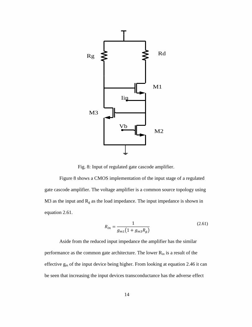
Fig. 8: Input of regulated gate cascode amplifier.
Figure 8 shows a CMOS implementation of the input stage of a regulated
gate cascode amplifier. The voltage amplifier is a common source topology using
M3 as the input and Rg as the load impedance. The input impedance is shown in
equation 2.61.
( )
(2.61)
Aside from the reduced input impedance the amplifier has the similar
performance as the common gate architecture. The lower Rin is a result of the
effective gm of the input device being higher. From looking at equation 2.46 it can
be seen that increasing the input devices transconductance has the adverse effect

15
of increasing the input referred noise, but with a large input capacitance this
circuit becomes the only option.
2.7 CHERRY-HOOPER DESIGN
The Cherry-Hooper topology was devised to allow the gain and bandwidth
of an amplifier to be tuned independently of each other. Figure 2.7 shows the
basic premise of the circuit. It is composed of two gm stages, the first input stage
which converts the input signal to a current and the second stage with a shunt
feedback resistor to convert the current (ix) into the output voltage.
gm1
gm2
RL CL
Rf
Vin Vout
ix
Fig. 9: The basic Cherry-Hooper topology.
(2.71)
⁄ ( ) (
*
(2.72)
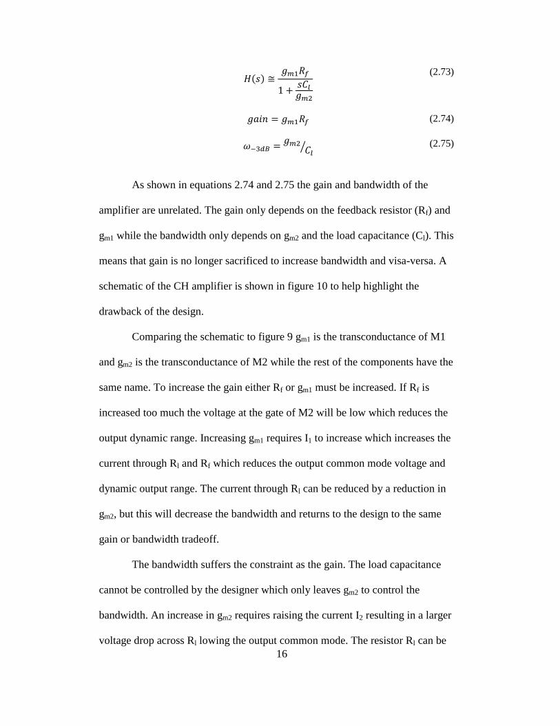
16
( )
(2.73)
(2.74)
⁄ (2.75)
As shown in equations 2.74 and 2.75 the gain and bandwidth of the
amplifier are unrelated. The gain only depends on the feedback resistor (Rf) and
gm1 while the bandwidth only depends on gm2 and the load capacitance (Cl). This
means that gain is no longer sacrificed to increase bandwidth and visa-versa. A
schematic of the CH amplifier is shown in figure 10 to help highlight the
drawback of the design.
Comparing the schematic to figure 9 gm1 is the transconductance of M1
and gm2 is the transconductance of M2 while the rest of the components have the
same name. To increase the gain either Rf or gm1 must be increased. If Rf is
increased too much the voltage at the gate of M2 will be low which reduces the
output dynamic range. Increasing gm1 requires I1 to increase which increases the
current through Rl and Rf which reduces the output common mode voltage and
dynamic output range. The current through Rl can be reduced by a reduction in
gm2, but this will decrease the bandwidth and returns to the design to the same
gain or bandwidth tradeoff.
The bandwidth suffers the constraint as the gain. The load capacitance
cannot be controlled by the designer which only leaves gm2 to control the
bandwidth. An increase in gm2 requires raising the current I2 resulting in a larger
voltage drop across Rl lowing the output common mode. The resistor Rl can be

17
reduced to compensate for the increased current, but it must remain larger than
1/gm2. The only to increase both gain and bandwidth is to increase the power
supply voltage which is not an option for a specified CMOS technology.
The Cherry-Hooper design essentially moves the design tradeoff from
gain and bandwidth to gain/bandwidth and dynamic range. The modified Cherry-
Hooper is presented next which alleviates this tradeoff.
RL
Rf Rf
ClCl
M1 M1
M2 M2
Vin+ Vin-
I2
I1
RL
Vout+ -
Fig. 10: Schematic of a Cherry-Hooper amplifier.

18
2.8 Modified CHERRY-HOOPER DESIGN
The limitation placed on the amplifier by the dynamic range can be
reduced by using a modified CH topology as shown in figure 10. A resistor
divider made by R1 and R2 is added to the feedback path. This means that only a
fraction of the output voltage is buffered fed back to the input. This allows the
designer to increase the gain of the amplifier as shown below without increasing
Rf or gm1 so there is no output dynamic range sacrifice.
gm1 gm2
CL R1
R2
Rf1
Vin VoutVx
Vy
Fig. 11: Modified Cherry-Hooper topology.
(2.76)
(
)
(2.77)
( ) (
*
(2.78)

19
( ) ( *(
( ),
(2.79)
(
*
(2.710)
( )
(2.711)
Equations 2.710 and 2.711 show the gain and -3dB point of the modified
CH amplifier. The gain is now increased by a factor of ⁄ while the
bandwidth is reduced by the same factor. Figure 12 shows a schematic for a
modified CH amplifier in CMOS. The added resistor divider is done with R2 and
R3 while M3 acts as a unity gain amplifier to isolate the feedback from the output.
This allows for the current through R1 and R2 to only come from I2 which helps
improve the dynamic range.

20
I1
I2
M1 M1
M2 M2
M3M3
Rf RfR2 R2
R3 R3
Vout
+ -
Vin+ Vin-
Fig. 12: A schematic of a modified CH amplifier.
With this schematic the gain can be improved by increasing I1 and gm1. To
keep the dynamic range constant Rf must be reduced. This loss in gain from
reducing Rf can be compensated for by increasing the ratio of R2 to R1. To make
up for the bandwidth decrease caused by R2 and R1, I2 can be increased. The
absolute value of R1 and R2 can be decreased to keep the output voltage constant
since only the ratio of the two impacts the gain and bandwidth. The only
drawback is that gm2*R1 must be much greater than one. This puts a limit on how
large I2 can be.

21
2.9 MODIFIED CHERRY-HOOPER AS A TIA
The modified CH amplifier can be easily adapted to a TIA design by
replacing gm1 with a common gate or regulated gate cascade input stage. This
topology with a common gate input is shown in figure 13. The input stage acts as
a buffer stage to provide low input impedance. As discussed in section 2.5 this
helps avoid the parasitic capacitance from the photodiode determining the
bandwidth of the system.
(2.81)
( )
(2.82)
(2.83)
(
⁄+
(2.84
⁄
(
*
(2.85)
22
CG gm2
1
Iin
Rf
R2R1CL
VoutVy Vx
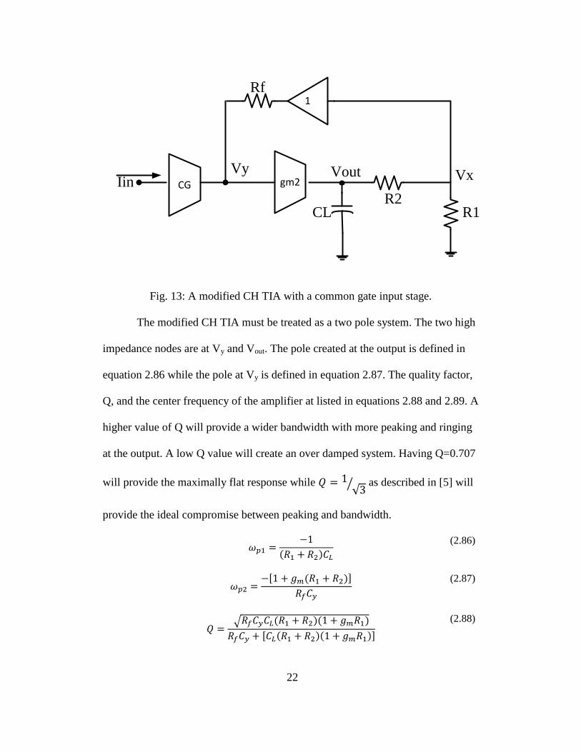
Fig. 13: A modified CH TIA with a common gate input stage.
The modified CH TIA must be treated as a two pole system. The two high
impedance nodes are at Vy and Vout. The pole created at the output is defined in
equation 2.86 while the pole at Vy is defined in equation 2.87. The quality factor,
Q, and the center frequency of the amplifier at listed in equations 2.88 and 2.89. A
higher value of Q will provide a wider bandwidth with more peaking and ringing
at the output. A low Q value will create an over damped system. Having Q=0.707
will provide the maximally flat response while √ ⁄ as described in [5] will
provide the ideal compromise between peaking and bandwidth.
( )
(2.86)
[ ( )]
(2.87)
√ ( )( )
[ ( )( )]
(2.88)

23
√
( )
(2.89)
CG CG
I+ I-
Vout
+ -
RfRfR2 R2
R1 R1
M2 M2
M3 M3
I2
Fig. 14: Schematic of a modified CH TIA.
The easiest way to analyze the noise is to see by inspection that the
modified CH TIA is very similar to the common gate topology. It uses a common
gate input followed by a voltage amplifier.
The second stage is similar to a shunt-shunt architecture which has a much
lower input referred noise than the common gate. For this design the noise is
dominated by the active devices in the common gate block and the feedback
resistance. Since the feedback resistance is a major contributor to the input
referred noise, the smaller value used in the modified CH creates a higher amount

24
of noise. The total input referred noise spectral density from the major
contributors is listed below.
, ,
(2.811)
2.10 LITERATURE REVIEW
There are many factors that make it difficult to compare TIA designs.
Many are designed as an analog front end for digital communications while few
are designed for use with an analog to digital converter for signal processing. This
leads to many different designs optimized in a variety of ways. Digital
communication receivers focus on high gain and wide bandwidth with noise and
linearity considerations only required to keep the BER low. A sampled analog
design has much stricter noise and linearity specifications and therefore have
lower gain bandwidth product. Naming conventions for the different topologies
also present another issue. It is common for one paper to refer to an amplifier as a
regulated gate cascade while it is actually a Cherry Hooper design with an RGC
input followed by a voltage amp with shunt-shunt feedback. Any design in this
comparison labeled combination is some form of common gate input followed by
a voltage amplifier with shunt feedback.
Table 2: Comparison of state of the art TIAs.
Reference Topology Technology Gain Bandwidth Noise CPD
[4] RGC .6µ 58dBΩ 860MHz 6.3pA/√
[6] Combination .18µ 87dBΩ 7.6GHz NR

25
[7] Combination .18µ 52dBΩ 3.9GHz NR
[8] Combination .25µ 80dBΩ 670MHz 13pA/√
[9] Combination .35µ 66dBΩ 256MHz NR
[10] RGC .8µ 120dBΩ 58MHz .5pA/√
[11] Combination .13µ 52dBΩ 4.2GHz NR
[12] Shunt-Shunt .18µ 70dBΩ 1GHz 4.5pA/√
26
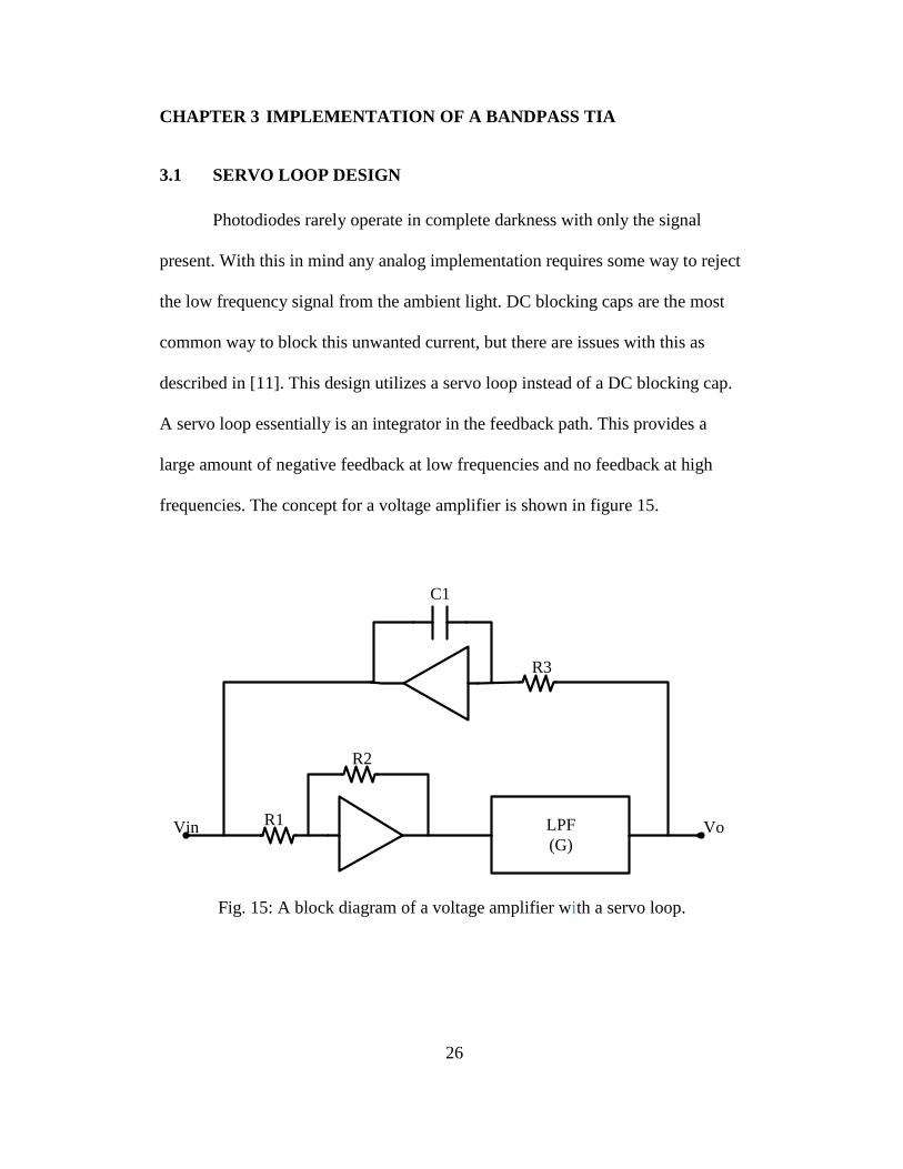
CHAPTER 3 IMPLEMENTATION OF A BANDPASS TIA
3.1 SERVO LOOP DESIGN
Photodiodes rarely operate in complete darkness with only the signal
present. With this in mind any analog implementation requires some way to reject
the low frequency signal from the ambient light. DC blocking caps are the most
common way to block this unwanted current, but there are issues with this as
described in [11]. This design utilizes a servo loop instead of a DC blocking cap.
A servo loop essentially is an integrator in the feedback path. This provides a
large amount of negative feedback at low frequencies and no feedback at high
frequencies. The concept for a voltage amplifier is shown in figure 15.
LPF
(G)Vin R1
R2
R3
C1
Vo
Fig. 15: A block diagram of a voltage amplifier with a servo loop.
27
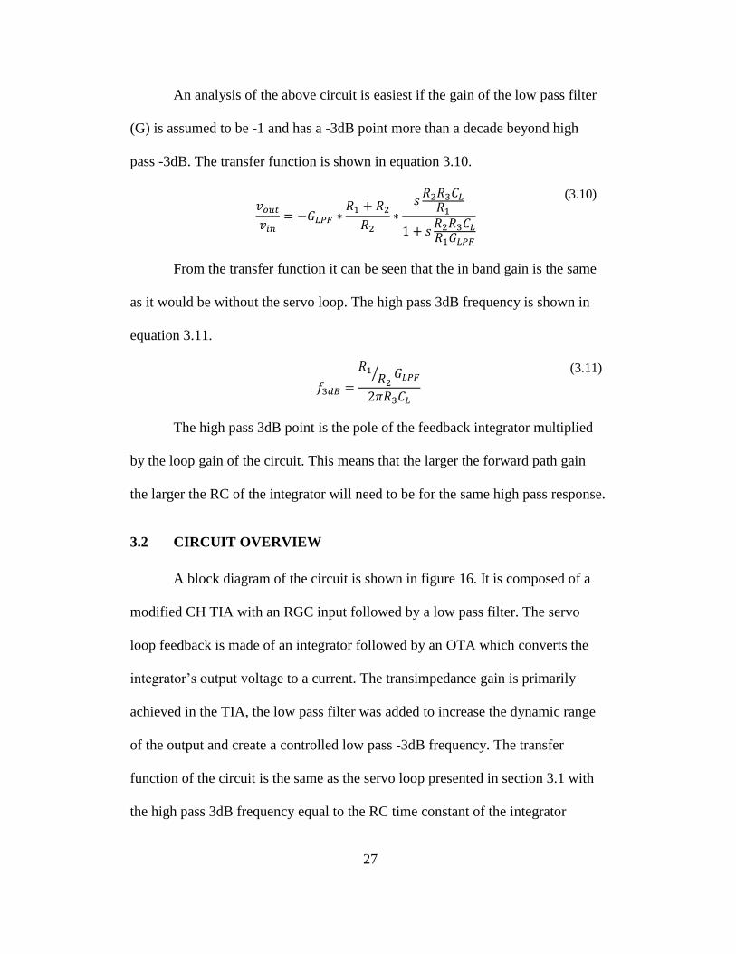
An analysis of the above circuit is easiest if the gain of the low pass filter
(G) is assumed to be -1 and has a -3dB point more than a decade beyond high
pass -3dB. The transfer function is shown in equation 3.10.
(3.10)
From the transfer function it can be seen that the in band gain is the same
as it would be without the servo loop. The high pass 3dB frequency is shown in
equation 3.11.
⁄
2
(3.11)
The high pass 3dB point is the pole of the feedback integrator multiplied
by the loop gain of the circuit. This means that the larger the forward path gain
the larger the RC of the integrator will need to be for the same high pass response.
3.2 CIRCUIT OVERVIEW
A block diagram of the circuit is shown in figure 16. It is composed of a
modified CH TIA with an RGC input followed by a low pass filter. The servo
loop feedback is made of an integrator followed by an OTA which converts the
integrator’s output voltage to a current. The transimpedance gain is primarily
achieved in the TIA, the low pass filter was added to increase the dynamic range
of the output and create a controlled low pass -3dB frequency. The transfer
function of the circuit is the same as the servo loop presented in section 3.1 with
the high pass 3dB frequency equal to the RC time constant of the integrator

28
multiplied by the loop gain of the circuit. The interesting thing in the proposed
circuit is the gm of the OTA in the feedback can be used to reduce the loop gain
of the circuit which helps reduce the size of R3 and C2.
OTA
Voltage Amp
Integrator
IinR1
R2
R3
C2
Modified CHTIA
Vout
C1
Fig. 16: Block diagram of the presented design.
Table 3: List of equations that define the presented circuits parameters.
Parameter Equation
Forward Gain (
*
Loop Gain (
*
Low Pass -3dB
Frequency
2

29
High Pass 3dB
Frequency
( )
2
3.3 DESIGN SPECIFICATIONS
The requirements of the circuit are presented in the table below.
Table 4: Design specifications for the TIA.
Parameter Specification
Transimpedance Gain (ZT) 210kΩ
Input Impedance (CPD) 0.8pF
Input Dynamic Range 4nA to 4µA
Output Dynamic Range 1mV to 1V
Input Referred Noise Density 0.35 √ ⁄
Bandwidth 15MHz to 35MHz
Gain Bandwidth Product 6.3THz*Ω
Dark Current 0 to 40µA
3.4 MODIFIED CHERRY-HOOPER TIA
Small devices were used throughout the design to allow for as wide a
bandwidth as possible. The dominant pole in the design occurs at Vx with the
second pole at the output. The bias currents through the RGC input were also
small to try and minimize noise. The current I1 is 18µA while the current I2 is
80µA. The Q value calculated using equation 2.88 is Q≈0.5 and the center

30
frequency is ω=1.3x10⁹ rad/s or f=192MHz. The calculated gain using equation
2.85 is ZT=167kΩ. The actual gain of the circuit is lower because the assumption
that ⁄ is not true. Even if the simplified gain equation were valid the
gain is still lower than the design requirement. The rest of the gain is made up for
in the voltage amplifier.
This stage plays a large part in setting the input referred noise of the entire
circuit. Equation 2.811 defines the noise of this amplifier and highlights the
primary drawback of the design. To avoid having the photodiode capacitance
define the bandwidth of the system the input impedance must be low and low
input impedance increases the noise. Pushing the pole at Vx to higher frequencies
requires a smaller feedback resistance. The gain is held constant by increasing the
ratio of R2 to R1, but the noise is increased. All of the benefits the modified CH
provides to increase the gain and bandwidth come with the penalty of increased
noise. A rough estimate of the input referred noise is shown below. This low
estimate already puts the noise ten times higher than the requirement.
,
2
, √
(3.40)

31
Vb1
Vb1
Vb1
Vb2
Vb2
Vb2
Vb3 Vb3
Rf Rf
R2
R1
R2
R1
M1 M1
M2 M2
M3 M3
M4
M5M6 M6
M7 M7
M8 M8
M9 M9
I1I1
I2
I3I3
In+ In-
Vout
+ -
Vx Vx
Fig. 17: Schematic of the presented TIA.
Table 5: Transistor sizes used in the TIA.
Transistor Width (W) Length (L)
M1 1.62µ 0.36µ
M2 0.9µ 0.18µ
M3 5.04µ 0.18µ
M4 7.56µ 0.36µ
M5 5.04µ 0.18µ
M6 2.52µ 0.18µ
M7 5.04µ 0.18µ
M8 5.04µ 0.18µ
M9 5.04µ 0.18µ

32
Table 6: Resistor values for the TIA schematic.
Resistor Value
Rf 20kΩ
R1 1.8kΩ
R2 15kΩ
3.5 OP AMP DESIGN
The opamp used in this design is a standard and well known design. It is
fully differential with a cross coupled class AB output stage. The design is shown
in figure 18, but since it is not critical portion further analysis is not shown. The
interested reader can find further details of the design in [3].
Vin+ Vin-
Vout-Vout+
VcVc
Fig. 18: Schematic of the opamp used in the LPF.

33
3.6 INTEGRATOR DESIGN
As with the opamp the integrator is not a new design. The same opamp
could have been used here, but there was a plan to attenuate the output voltage
before connecting it to the feedback to lower the size of the RC network. This
attenuation would have shifted the DC level of the input to the integrator nearly to
ground. With this in mind a PMOS input pair was used to accommodate the low
input voltage. It is a standard folded cascade amplifier.
Vc Vc
Vin- Vin+Vo+ Vo-
Fig. 19: Schematic of the amplifier used in the integrator.
34
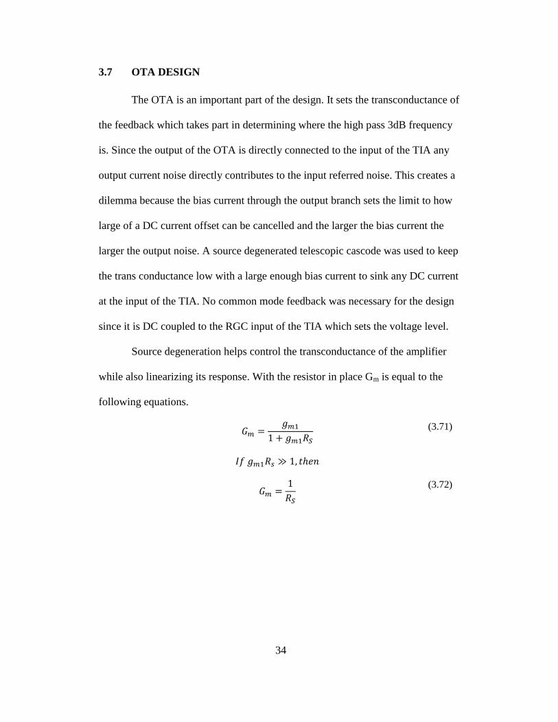
3.7 OTA DESIGN
The OTA is an important part of the design. It sets the transconductance of
the feedback which takes part in determining where the high pass 3dB frequency
is. Since the output of the OTA is directly connected to the input of the TIA any
output current noise directly contributes to the input referred noise. This creates a
dilemma because the bias current through the output branch sets the limit to how
large of a DC current offset can be cancelled and the larger the bias current the
larger the output noise. A source degenerated telescopic cascode was used to keep
the trans conductance low with a large enough bias current to sink any DC current
at the input of the TIA. No common mode feedback was necessary for the design
since it is DC coupled to the RGC input of the TIA which sets the voltage level.
Source degeneration helps control the transconductance of the amplifier
while also linearizing its response. With the resistor in place Gm is equal to the
following equations.
(3.71)
,
(3.72)
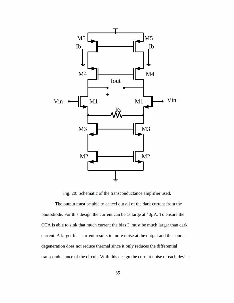
35
Iout
+ -Vin- Vin+
Rs
Ib Ib
M1 M1
M2 M2
M3 M3
M4 M4
M5 M5
Fig. 20: Schematic of the transconductance amplifier used.
The output must be able to cancel out all of the dark current from the
photodiode. For this design the current can be as large at 40µA. To ensure the
OTA is able to sink that much current the bias Ib must be much larger than dark
current. A larger bias current results in more noise at the output and the source
degeneration does not reduce thermal since it only reduces the differential
transconductance of the circuit. With this design the current noise of each device

36
directly adds to the output of the amplifier. The total output thermal noise is
calculated in equation 3.71.
,
(3.71)
, √

37
CHAPTER 4 SIMULATION RESULTS
4.1 TIA CHARACTERIZATION
With the servo loop design the photodiode is DC coupled to the input of
the TIA. Because of this the bias voltage across the diode is fixed by the input
common mode voltage of the TIA. The downside is the diode cannot be placed
across the differential inputs of the TIA and have a reverse DC bias. Figure 21
shows the test bench used in simulation. There is no available model for the
photodiode available so another diode made with the same process was used to
mimic any leakage current. The capacitor C1 is the parasitic capacitance of the
photodiode while C2 is connected to the other input to balance the two.
TIA
I AC
+-
-+
D1 C1C2
CL CL
Fig. 21: Test bench for the TIA.
The –3dB frequency and gain for the TIA are shown in figure 22. The gain
is 70.8kΩ (97dBΩ) and the roll off frequency is 98MHz. The system gain
specification is 210kΩ and the TIA alone does not achieve this. The LPF provides
the rest of the gain for the system. The input referred noise spectral density is
shown in figure 23. In the pass band the noise varies from √ ⁄ to

38
√ ⁄ which closely agrees with the thermal noise calculated in equation
3.40.
Fig. 22: Gain and bandwidth of the TIA.
Fig. 23: Input referred noise of the TIA.
The distortion of the TIA should also set the total distortion of the circuit.
It is performing a single ended to differential conversion which causes the
distortion to be largely based on the bias current of the input device. This bias

39
current was intentionally made low to lower the noise of the amplifier, but also
must be high to avoid distortion issues. The plot below shows the intermodulated
distortion caused by two input signals with half the input dynamic range. The
frequency of these signals are 20MHz and 21MHz. While there was no given
specification for linearity the goal was to get the IMD below 70dB.
Fig. 24: Third order intermodulated distortion of the TIA.
4.2 CHARACTERIZATION OF THE LPF
The main purpose of the LPF is to set the low pass -3dB frequency and
provide a large output signal swing. It also must not limit the circuit in any way.
For this to be true the distortion of the filter must be less than the TIA distortion
and the noise must be a minor contributor to the overall input referred noise.
Figure 25 shows the test bench for the LPF. For the distortion simulation the input
voltage was set to the maximum output swing of the TIA. In this test that swing is
-90
-80
-70
-60
-50
-40
-30
-20
-10
0
0 5 10
15
20
25
30
35
40
45
50
55
60
65
70
Sign
al A
mp
litu
de
(d
B)
Frequency (MHz)

40
4µA*ZT which is 285mVp-p. The gain of the LPF is set to 4 to provide a 1.14Vp-p
output voltage which is slightly more than the 1Vp-p specification.
To measure the LPF’s impact on the overall noise it must be referred back
to the input of the TIA. This is done by dividing the input referred noise of the
LPF by the transimpedance gain of the TIA as shown in equation 4.21.
,
,
(4.21)
The noise spectral density at the TIA input caused by the LPF is shown in
figure 27. The noise is much smaller than the total input referred noise of the
system so the LPF is minor contributor.
Fig. 25: Gain and bandwidth of the LPF.

41
Fig. 26: Input referred noise at the TIA caused by the LPF.

42
4.3 CHARACTERIZATION OF THE INTEGRATOR
The integrator sets the 3dB high pass frequency and is subject to the same
constraints as the LPF. The noise must not be a major contributor and the
distortion must also be less than the TIA distortion. Because it is in the feedback
loop the output referred noise of the circuit is important. The output referred
voltage noise of the integrator is multiplied by the Gm of the OTA to calculate the
input referred noise of the TIA.
Fig. 27: Gain and bandwidth of the integrator.

43
Fig. 28: The spectral density of the integrator noise referred to the TIA input.
4.4 CHARACTERIZATION OF THE OTA
The purpose of the OTA is to convert the feedback voltage to a current.
The important parameters for this stage are the transconductance and input
referred noise. Since the output is directly connected to the input of the TIA any
noise in this circuit will be a major contributor to the total input referred noise.
The output noise current density was calculated by simulated the input referred
noise of the circuit and multiplying it by the transconductance of the circuit. At
low frequency the flicker noise of the active devices is dominant. Once the
thermal noise dominants it closely matches the noise calculated in equation 3.71
of √ ⁄ .

44
Fig. 29: The spectral density of the OTA noise referred to the input of the TIA.
4.5 CHARACTERIZATION OF THE COMPLETE CIRCUIT
The gain and bandwidth of the complete system are shown in figure 31.
From it the high pass 3dB frequency is 5MHz, while the low pass -3dB frequency
is 45MHz. The frequencies are wider than the required bandwidth of the system to
avoid any compression within the passband. If a more tightly controlled
bandwidth is required higher order analog filters may be used or digital filtering
techniques can be employed after the ADC. The peak gain in the passband is
about 106dBΩ or 200kΩ. This is slightly below the required gain and can be
attributed the loading of the TIA by the LPF.

45
Fig. 30: Gain and bandwidth of complete circuit.
One method for testing the DC offset cancellation is to provide a stair step
input current and monitor the output. The benefit to this method is that it also tests
the design for stability. If the phase margin of the design was too low ringing
would be present at the output. A small amount is noticed when the input current
jumps from 32µA to 40µA. This is mostly likely caused by the output of the OTA
saturating. The high pass and low pass frequencies can be extracted by measuring
the rise and fall times of the output.

46
Fig. 31: Transient simulation of complete current showing DC offset cancellation
and stability.
Fig. 32: Superposition of all noise sources compared to total input referred noise.
Figure 33 shows how much each circuit block contributes to the total input
referred noise of the system in the pass band. It shows the OTA is the primary
-4.5E-05
-4.0E-05
-3.5E-05
-3.0E-05
-2.5E-05
-2.0E-05
-1.5E-05
-1.0E-05
-5.0E-06
0.0E+00
0
0.2
0.4
0.6
0.8
1
1.2
1.4
1.6
0
84
21
1
33
3
45
5
58
2
70
5
82
7
95
4
1,0
76
1,2
01
1,3
23
1,4
50
1,5
72
1,6
97
1,8
21
1,9
46
2,0
68
2,1
93
2,3
20
2,4
43
2,5
65
2,6
92
2,8
14
2,9
36
Am
ps
Vo
lts
Time (ps)
Vout- Vout+ Input Current

47
source of noise until higher frequencies where the TIA becomes the dominant
contributor.
Fig. 33: The intermodulated distortion of the complete circuit.
The linearity of the entire circuit is demonstrated in figure 34. Similar to
the test for the TIA a single ended input is provided. Each input has an amplitude
of 2µA and they are at 20MHz and 21MHz. The SFDR of the system is 48dB,
slightly below the design goal of 50dB.
. Two transient simulations with a single ended input with an amplitude of
4µA and frequency of 20MHz are shown in figures 34 and 35. Figure 34 shows
the output response without any DC input offset. It shows both the positive and
negative terminal and the difference between the two.
-120
-100
-80
-60
-40
-20
0
0 5
10
15
20
25
30
35
40
45
50
55
60
65
70
75
80
85
90
95
10
0
Sign
al A
mp
litu
de
(d
B)
Frequency (MHz)

48
Fig. 34: Transient output simulation.
Fig. 35: Transient simulation with slow rising DC offset of 0A to 40µA.
Figure 35 shows the output while a slowly increasing DC offset is added
the input. The input is composed of a current signal with a 4µA amplitude at
20MHz on top of a 0-40µA ramp over 10µs. Some output distortion shows up
-1
-0.5
0
0.5
1
1.5
0.0
E+0
0
4.0
E-0
9
4.4
E-0
8
5.4
E-0
8
9.2
E-0
8
1.3
E-0
7
1.7
E-0
7
2.1
E-0
7
2.5
E-0
7
2.9
E-0
7
3.3
E-0
7
3.7
E-0
7
4.1
E-0
7
4.5
E-0
7
4.9
E-0
7
5.3
E-0
7
5.7
E-0
7
6.0
E-0
7
6.4
E-0
7
6.8
E-0
7
7.2
E-0
7
7.6
E-0
7
8.0
E-0
7
8.4
E-0
7
8.8
E-0
7
9.2
E-0
7
9.6
E-0
7
1.0
E-0
6
Am
plit
ud
e (
V)
Time (s)
Difference Out+ Out-
-1-0.8-0.6-0.4-0.200.20.40.60.81
-1.0E-05
0.0E+00
1.0E-05
2.0E-05
3.0E-05
4.0E-05
5.0E-05
0.0
E+0
04
.0E-
07
8.5
E-0
71
.3E-
06
1.8
E-0
62
.2E-
06
2.7
E-0
63
.1E-
06
3.6
E-0
64
.1E-
06
4.5
E-0
65
.0E-
06
5.4
E-0
65
.9E-
06
6.4
E-0
66
.8E-
06
7.3
E-0
67
.7E-
06
8.2
E-0
68
.7E-
06
9.1
E-0
69
.6E-
06
Ou
tpu
t V
olt
age
(V
)
Inp
ut
Cu
rre
nt
(A)
Time (s)
Input Output

49
with an input offset of 30µA. This distortion could have been reduced by
increasing the bias current of the OTA, but would have resulted in larger input
referred noise. The noise contribution from the OTA is explained in section 3.7
and shows how the bias current and noise are directly proportional.
Figure 36 shows the output current of the OTA with the same input used
for figure 35. The purpose of this graph is show how any DC offset at the input of
the TIA is compensated for by the feedback OTA. The single ended to differential
conversion is shown as each output of the OTA sinks half of the offset current. A
complete summary of the system performance and design specifications is shown
in table 6.
Fig. 36: Transient simulation showing input DC offest and feedback current
through the OTA.
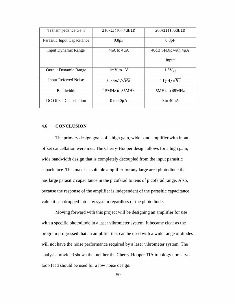
Table 7: Summary of the system performance and design specifications.
Parameter Specification Simulated Value
-3.0E-05
-2.0E-05
-1.0E-05
0.0E+00
1.0E-05
2.0E-05
3.0E-05
4.0E-05
5.0E-05
0.0
E+0
0
3.4
E-0
7
7.4
E-0
7
1.1
E-0
6
1.5
E-0
6
1.9
E-0
6
2.3
E-0
6
2.8
E-0
6
3.2
E-0
6
3.6
E-0
6
4.0
E-0
6
4.4
E-0
6
4.8
E-0
6
5.2
E-0
6
5.6
E-0
6
6.0
E-0
6
6.4
E-0
6
6.8
E-0
6
7.2
E-0
6
7.6
E-0
6
8.0
E-0
6
8.4
E-0
6
8.8
E-0
6
9.2
E-0
6
9.6
E-0
6
Cu
rre
nt
(A)
Time (s)
Input FB+ FB-
50
Transimpedance Gain 210kΩ (106.4dBΩ) 200kΩ (106dBΩ)
Parasitic Input Capacitance 0.8pF 0.8pF
Input Dynamic Range 4nA to 4µA 48dB SFDR with 4µA
input
Output Dynamic Range 1mV to 1V 1.5Vp-p
Input Referred Noise 0.35 √ ⁄ √ ⁄
Bandwidth 15MHz to 35MHz 5MHz to 45MHz
DC Offset Cancellation 0 to 40µA 0 to 40µA
4.6 CONCLUSION
The primary design goals of a high gain, wide band amplifier with input
offset cancellation were met. The Cherry-Hooper design allows for a high gain,
wide bandwidth design that is completely decoupled from the input parasitic
capacitance. This makes a suitable amplifier for any large area photodiode that
has large parasitic capacitance in the picofarad to tens of picofarad range. Also,
because the response of the amplifier is independent of the parasitic capacitance
value it can dropped into any system regardless of the photodiode.
Moving forward with this project will be designing an amplifier for use
with a specific photodiode in a laser vibrometer system. It became clear as the
program progressed that an amplifier that can be used with a wide range of diodes
will not have the noise performance required by a laser vibrometer system. The
analysis provided shows that neither the Cherry-Hooper TIA topology nor servo
loop feed should be used for a low noise design.

REFERENCES
[1] C. Hermans and M. Steyaert, “Broadband Opto-Electrical Receivers in Standard CMOS”,
pp.61-103, Springer, 2007
[2] W.M.C Sansen, “Analog Design Essentials”, Springer, 2006
[3] R. J. Baker, “CMOS Circuit Design, Layout, and Simulation”, John Wiley & Sons, Inc.,
2008
[4] S. M. Park, “1.25-Gb/s regulated cascode CMOS transimpedance amplifier for Gigabit
Ethernet applicatinos”, IEEE Journal of Solid-State Circuits, pp. 112, Jan. 1, 2004
[5] Holdenried, “Analysis and design of HBT Cherry Hooper amplifier with emitter follower
feedback for optical communication”
[6] W.-Z. Chen, Y.-L. Cheng, D.-S. Lin, “A 1.8V 10Gb/s fully integrated CMOS optical
receiver analog front-end”, IEE Journal of Solid-State Circuits, pp. 1388-1396, June 2005
[7] H.-Y. Hwang, J.-C. Chien, T.-Y. Chen, L.-H. Lu, “A CMOS tunable transimpedance
amplifier,” IEEE Microwave Wireless Components Letters, pp. 693-695, Dec. 2006
[8] J. Lee, S.-J. Song, S.M. Park, C.-M. Nam, Y.-S. Kwon, H.-J. Yoo, “A multichip on oxide
of 1Gb/s 80dB fully-differential CMOS transimpedance amplifier for optical interconnect
applications,” IEEE International Solid-State Circuits Conference, Feb. 2002
[9] R.Y. Chen, T.-S. Hung, C.-Y. Hung, “A CMOS infrared wireless optical receiver front-
end with a variable-gain fully-differential transimpedance amplifier,” IEEE Transactions
on Consumer Electronics, pp.424-429, May 2005
[10] S. Goswami, J. Silver, T. Copani, W. Chen, H. J. Barnaby, B. Vermeire, S. Kiaei,
“A 14mW 5Gb/s CMOS TIA with gain-reuse regulated cascade compensation for
parallel optical interconnects,” IEEE International Solid-State Circuits Conference, Feb.
2009
[11] M. Fortunato, “A new filter topology for analog high-pass filters”, TI Analog
Applications Journal, pp. 18-24, 3Q, 2008
[12] Bespalko, R (2007) Transimpedance Amplifier Design using 0.18µm CMOS
Technology, unpublished thesis (M.S), Queen’s University
[13] Chandrashekar, K (2007) Wide Bandwidth Transimpedance Amplifier using
Modified Cherry Hooper Amplifier, unpublished thesis (M.S), Arizona State University

[14] Abe, T. and Sugimoto, T, “Extremely shallow underground imagining using
scanning laser Doppler vibrometer”, Japanese Journal of Applied Physics, Vol. 28, Issue
7, 2009
Top Related