


Languages
Pages
Legal

DESIGN AND IMPLEMENTATION OF AN
ETSI-SDR OFDM TRANSMITTER WITH
POWER AMPLIFIER LINEARIZER
A Thesis
Submitted to the College of Graduate Studies and Research
in Partial Fulfillment of the Requirements
for the Degree of Master of Science
in the Department of Electrical Engineering
University of Saskatchewan
Saskatoon, Saskatchewan, Canada
By
SURANJANA JULIUS
Copyright Suranjana Julius, September, 2010. All rights reserved.

i
PERMISSION TO USE
The author has agreed that the Library, University of Saskatchewan, may make
this thesis freely available for inspection. Moreover, the author has agreed that
permission for extensive copying of this thesis for scholarly purposes may be granted
by the professors who supervised this thesis work, Prof. Anh Dinh or in his absence, by
the Head of the Department of Electrical and Computer Engineering or the Dean of the
College of Graduate Studies and Research at The University of Saskatchewan. It is
however expected that due recognition will be given to the author and the University of
Saskatchewan in any use of this thesis in whole or in part. Copying, publication or use
of this thesis or parts thereof for financial gain shall not be allowed without the author‟s
written permission.
Request for permission to copy or to make use of material in this thesis in whole
or in part should be addressed to:
Head of the Department of Electrical Engineering
57 Campus Drive
University of Saskatchewan
Saskatoon, Saskatchewan, Canada
S7N 5A9

ii
ACKNOWLEDGMENTS
I express my sincere gratitude to my supervisor, Prof. Anh Dinh, for the
guidance and encouragement that he provided throughout my research and throughout
the course of my graduate program. I thank Prof. Ron Bolton for this
Telecommunications Research Laboratories (TRLABS) research opportunity and his
continued encouragement. I would also like to thank the rest of my advisory committee
members: Mr. Dennis Akins (SED), Mr. Dale Gunderson (SED) and Mr. Andrew
Kostiuk (TRLABS) for contributions throughout my research.
A special thanks to SED Systems for this project. I wish to thank TRLABS for
providing me with financial assistance and the great research environment.
Special thanks to Mr. David Armstrong and Mr. Daryl Warkentin from SED
Systems for their valuable suggestions throughout my research. Thanks to Mr. Jack
Hanson (TRLABS) for my research platform and Ms. Vera Ljubovic (TRLABS) for all
her support and encouragement.
Thanks to College of Graduate Studies and Research and all the professors, staff
and my fellow graduate students in the Department of Electrical Engineering who
helped me in various stages of my graduate program.
Thanks to my parents for always being there for me. Thanks to my brother-in-
law, Bijoy, for being a role model and always believing in me. Finally, I thank the very
special person in my life, my beloved husband and best friend, Gary, who has been my
rock through all the highs and lows.
iii
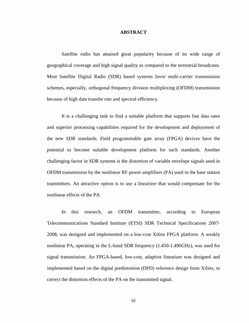
ABSTRACT
Satellite radio has attained great popularity because of its wide range of
geographical coverage and high signal quality as compared to the terrestrial broadcasts.
Most Satellite Digital Radio (SDR) based systems favor multi-carrier transmission
schemes, especially, orthogonal frequency division multiplexing (OFDM) transmission
because of high data transfer rate and spectral efficiency.
It is a challenging task to find a suitable platform that supports fast data rates
and superior processing capabilities required for the development and deployment of
the new SDR standards. Field programmable gate array (FPGA) devices have the
potential to become suitable development platform for such standards. Another
challenging factor in SDR systems is the distortion of variable envelope signals used in
OFDM transmission by the nonlinear RF power amplifiers (PA) used in the base station
transmitters. An attractive option is to use a linearizer that would compensate for the
nonlinear effects of the PA.
In this research, an OFDM transmitter, according to European
Telecommunications Standard Institute (ETSI) SDR Technical Specifications 2007-
2008, was designed and implemented on a low-cost Xilinx FPGA platform. A weakly
nonlinear PA, operating in the L-band SDR frequency (1.450-1.490GHz), was used for
signal transmission. An FPGA-based, low-cost, adaptive linearizer was designed and
implemented based on the digital predistortion (DPD) reference design from Xilinx, to
correct the distortion effects of the PA on the transmitted signal.

iv
TABLE OF CONTENTS
PERMISSION TO USE ..................................................................................................... i
ACKNOWLEDGMENTS ................................................................................................. ii
ABSTRACT ...................................................................................................................... iii
TABLE OF CONTENTS ................................................................................................. iv
LIST OF TABLES .......................................................................................................... viii
LIST OF FIGURES .......................................................................................................... ix
LIST OF ABBREVIATIONS ......................................................................................... xii
1. INTRODUCTION ......................................................................................................... 1
1.1 Background of Research ............................................................................................ 2
1.1.1 Motivation ........................................................................................................ 2
1.1.2 Scope of Research ............................................................................................ 4
1.2 Research Objectives and Applied Methodology ....................................................... 5
1.2.1 Research Objectives ......................................................................................... 5
1.2.2 Applied Methodology ....................................................................................... 6
1.3 Thesis Outline ............................................................................................................ 7
1.4 Summary .................................................................................................................... 9
2. OFDM TRANSMISSION AND SIGNAL DISTORTION ...................................... 10
2.1 OFDM Transmission ............................................................................................... 10
2.1.1 Basic Principles of OFDM transmission ........................................................ 10
2.1.2 Digital Modulation Schemes .......................................................................... 12
2.2 Power Amplifier Nonlinearity and Signal Distortion .............................................. 16
2.2.1 PA Efficiency vs. Linearity ............................................................................ 16

v
2.2.2 PA Nonlinear Characteristics ......................................................................... 17
2.2.3 Intermodulation distortion and Spectral Regrowth ........................................ 20
2.3 Summary .................................................................................................................. 22
3. LINEARIZATION TECHNIQUES ........................................................................... 24
3.1 Biasing Methods ...................................................................................................... 25
3.1.1 Boot up Bias ................................................................................................... 25
3.1.2 Dynamic Bias ................................................................................................. 27
3.2 Envelope Elimination and Restoration .................................................................... 28
3.3 Feedback Methods ................................................................................................... 30
3.3.1 RF Feedback .................................................................................................. 30
3.3.2 Baseband Feedback ....................................................................................... 30
3.3.3 Polar Feedback .............................................................................................. 31
3.3.4 Cartesian Feedback ........................................................................................ 32
3.4 Feed-forward Method .............................................................................................. 34
3.5 Linear Amplification with Nonlinear Components ................................................. 35
3.6 Distortion Methods .................................................................................................. 37
3.6.1 Postdistortion ................................................................................................. 34
3.6.2 Predistortion .................................................................................................. 38
3.7 Digital Predistortion ................................................................................................ 40
3.8 Summary ................................................................................................................. 41
4. DESIGN OF TRANSMITTER AND LINEARIZER ............................................. 43
4.1 Design of OFDM Transmitter ................................................................................. 43
4.1.1 ETSI TS 102 551-2 V2.1.1 (2007-2008) ....................................................... 43
4.1.2 Data Generation and OFDM transmission ..................................................... 44
vi
4.2 Design of Linearizer System ................................................................................... 49
4.2.1 Digital Predistorter Characteristics ................................................................ 50
4.2.2 Digital Predistorter Functionality .................................................................. 52
4.2.3 Digital Predistortion based Linearizer system ............................................... 52
4.2.4 Integration of OFDM transmitter and Linearizer system .............................. 55
4.3 Summary ................................................................................................................. 58
5. SIMULATION ............................................................................................................ 60
5.1 Modeling of Power Amplifier ................................................................................. 60
5.1.1 AM-AM and AM-PM Characterization ......................................................... 60
5.1.2 Polynomial Curve-fitting ................................................................................ 61
5.2 Simulation and Results ........................................................................................... 66
5.2.1 System Integration and Simulation ................................................................ 66
5.2.2 Results ............................................................................................................ 68
5.3 Summary .................................................................................................................. 68
6. IMPLEMENTATION, RESULTS AND ANALYSIS .............................................. 70
6.1 Hardware Implementation ....................................................................................... 70
6.1.1 FPGA Implementation of OFDM Transmitter and DPD Linearizer .............. 70
6.1.2 Transmission Path .......................................................................................... 75
6.1.3 L-Band Power Amplifier ................................................................................ 78
6.1.4 Feedback Path ................................................................................................. 80
6.2 Results and Analysis ................................................................................................ 83
6.2.1 Transmitter Performance ................................................................................ 83
6.2.2 Power Amplifier Performance without and with Linearization ..................... 86
6.2.3 FPGA Resource Utilization ............................................................................ 90

vii
6.2.4 Comparison with Previous work .................................................................... 91
6.3 Summary .................................................................................................................. 94
7. CONCLUSIONS AND FUTURE WORK ................................................................. 96
7.1 Conclusions ............................................................................................................. 96
7.2 Future Work ............................................................................................................. 99
REFERENCES .............................................................................................................. 101
APPENDIX A ................................................................................................................ 106
APPENDIX B ................................................................................................................ 108
APPENDIX C ................................................................................................................ 110
viii
LIST OF TABLES
Table 3.1 Linearization schemes ....................................................................................... 26
Table 4.1 ETSI TS 102 551-2 Mode-3 OFDM parameters ............................................... 45
Table 4.2 Interpolating Filter design specifications .......................................................... 57
Table 5.1 Experimental data of PA input, output and phase-shift relationship ................. 62
Table 5.2 AM-AM and AM-PM curve-fit statistics .......................................................... 63
Table 5.3 AM-AM and AM-PM curve-fit coefficients ..................................................... 64
Table 6.1 Design clock rates ............................................................................................. 74
Table 6.2 Resource utilization on Xilinx Virtex-4 XCV4SX35 FPGA ............................ 91
Table 6.3 OFDM transmitter resource usage comparison of [11], [12] and this work ..... 92
Table A Galois type LFSR specifications [39] .............................................................. 107
ix
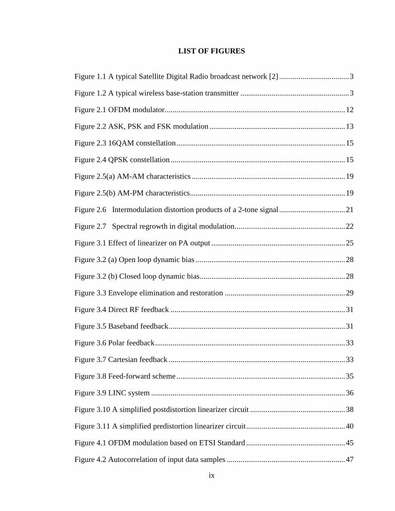
LIST OF FIGURES
Figure 1.1 A typical Satellite Digital Radio broadcast network [2] .................................... 3
Figure 1.2 A typical wireless base-station transmitter ........................................................ 3
Figure 2.1 OFDM modulator ............................................................................................. 12
Figure 2.2 ASK, PSK and FSK modulation ...................................................................... 13
Figure 2.3 16QAM constellation ....................................................................................... 15
Figure 2.4 QPSK constellation .......................................................................................... 15
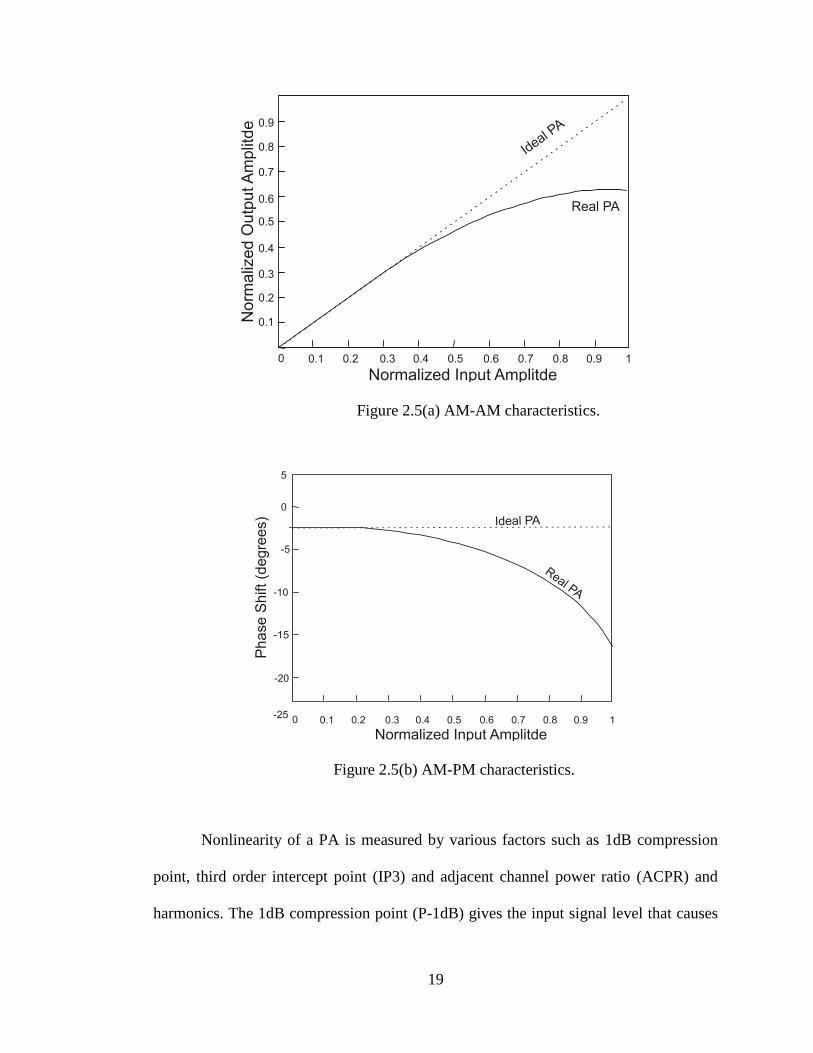
Figure 2.5(a) AM-AM characteristics ............................................................................... 19
Figure 2.5(b) AM-PM characteristics ................................................................................ 19
Figure 2.6 Intermodulation distortion products of a 2-tone signal .................................. 21
Figure 2.7 Spectral regrowth in digital modulation ......................................................... 22
Figure 3.1 Effect of linearizer on PA output ..................................................................... 25
Figure 3.2 (a) Open loop dynamic bias ............................................................................. 28
Figure 3.2 (b) Closed loop dynamic bias ........................................................................... 28
Figure 3.3 Envelope elimination and restoration .............................................................. 29
Figure 3.4 Direct RF feedback .......................................................................................... 31
Figure 3.5 Baseband feedback ........................................................................................... 31
Figure 3.6 Polar feedback .................................................................................................. 33
Figure 3.7 Cartesian feedback ........................................................................................... 33
Figure 3.8 Feed-forward scheme ....................................................................................... 35
Figure 3.9 LINC system .................................................................................................... 36
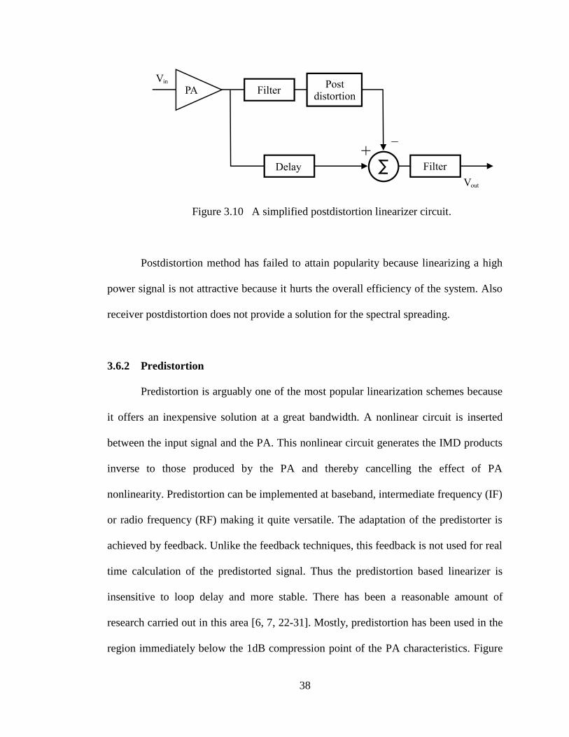
Figure 3.10 A simplified postdistortion linearizer circuit ................................................. 38
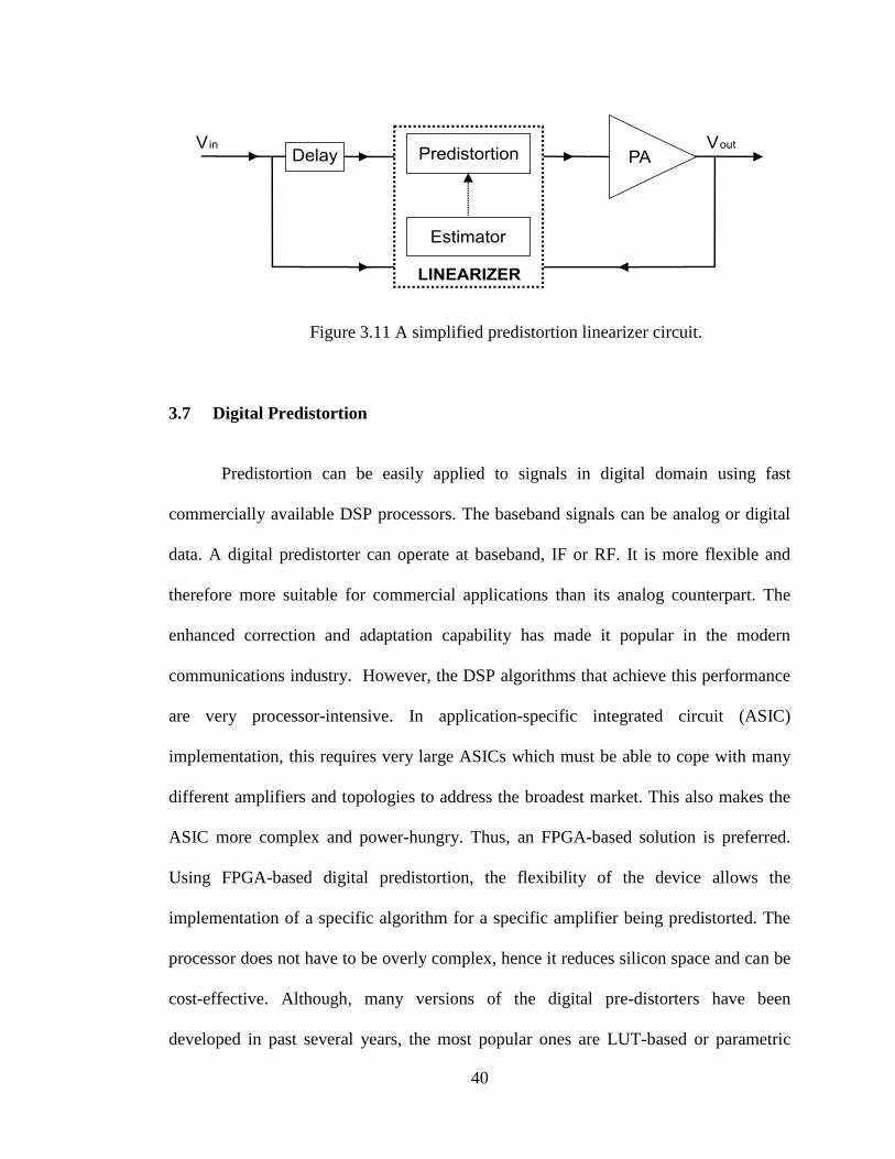
Figure 3.11 A simplified predistortion linearizer circuit ................................................... 40
Figure 4.1 OFDM modulation based on ETSI Standard ................................................... 45
Figure 4.2 Autocorrelation of input data samples ............................................................. 47
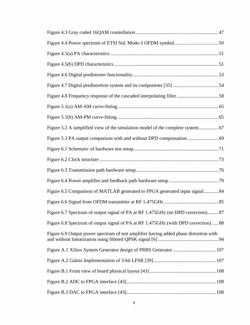
x
Figure 4.3 Gray coded 16QAM constellation ................................................................... 47
Figure 4.4 Power spectrum of ETSI Std. Mode-3 OFDM symbol .................................... 50
Figure 4.5(a) PA characteristics ........................................................................................ 51
Figure 4.5(b) DPD characteristics ..................................................................................... 51
Figure 4.6 Digital predistorter functionality ...................................................................... 53
Figure 4.7 Digital predistortion system and its components [35] ..................................... 54
Figure 4.8 Frequency response of the cascaded interpolating filter .................................. 58
Figure 5.1(a) AM-AM curve-fitting .................................................................................. 65
Figure 5.1(b) AM-PM curve-fitting .................................................................................. 65
Figure 5.2 A simplified view of the simulation model of the complete system ................ 67
Figure 5.3 PA output comparison with and without DPD compensation ......................... 69
Figure 6.1 Schematic of hardware test setup ..................................................................... 71
Figure 6.2 Clock structure ................................................................................................. 73
Figure 6.3 Transmission path hardware setup ................................................................... 76
Figure 6.4 Power amplifier and feedback path hardware setup ........................................ 79
Figure 6.5 Comparison of MATLAB generated to FPGA generated input signal ............ 84
Figure 6.6 Signal from OFDM transmitter at RF 1.475GHz ............................................ 85
Figure 6.7 Spectrum of output signal of PA at RF 1.475GHz (no DPD correction) ......... 87
Figure 6.8 Spectrum of output signal of PA at RF 1.475GHz (with DPD correction) ..... 88
Figure 6.9 Output power spectrum of test amplifier having added phase distortion with
and without linearization using filtered QPSK signal [6] ................................................. 94
Figure A.1 Xilinx System Generator design of PRBS Generator ................................... 107
Figure A.2 Galois Implementation of 3-bit LFSR [39] ................................................... 107
Figure B.1 Front view of board physical layout [43] ...................................................... 108
Figure B.2 ADC to FPGA interface [43] ......................................................................... 108
Figure B.3 DAC to FPGA interface [43] ......................................................................... 108

xi
Figure B.4 DAC (AD9772A) single-ended DC-coupled output [43] ............................. 109
Figure C Single-to-differential conversion of signal with 400mV DC bias addition
[46] ................................................................................................................................. 110

xii
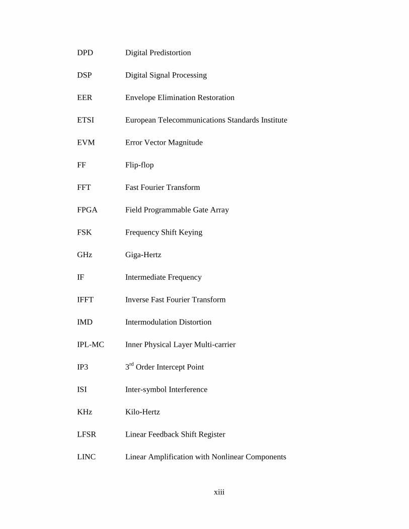
LIST OF ABBREVIATIONS
ACI Adjacent Channel Interference
ACPR Adjacent Channel Power Ratio
ADC Analog to Digital Converter
AM-AM Amplitude Modulation-Amplitude Modulation
AM-PM Amplitude Modulation-Phase Modulation
ASIC Application-specific integrated circuit
ASK Amplitude Shift Keying
BPSK Binary Phase-shift Keying
BRAM Block RAM
CFR Crest Factor Reduction
DAB Digital Audio Broadcasting
DAC Digital to Analog Converter
dB Decibel
dBm Power ratio in decibels referenced to 1 milli-watt
dBFS Decibels relative to Full Scale
DC Direct Current
DCM Digital Clock Manager
xiii
DPD Digital Predistortion
DSP Digital Signal Processing
EER Envelope Elimination Restoration
ETSI European Telecommunications Standards Institute
EVM Error Vector Magnitude
FF Flip-flop
FFT Fast Fourier Transform
FPGA Field Programmable Gate Array
FSK Frequency Shift Keying
GHz Giga-Hertz
IF Intermediate Frequency
IFFT Inverse Fast Fourier Transform
IMD Intermodulation Distortion
IPL-MC Inner Physical Layer Multi-carrier
IP3 3rd
Order Intercept Point
ISI Inter-symbol Interference
KHz Kilo-Hertz
LFSR Linear Feedback Shift Register
LINC Linear Amplification with Nonlinear Components
xiv
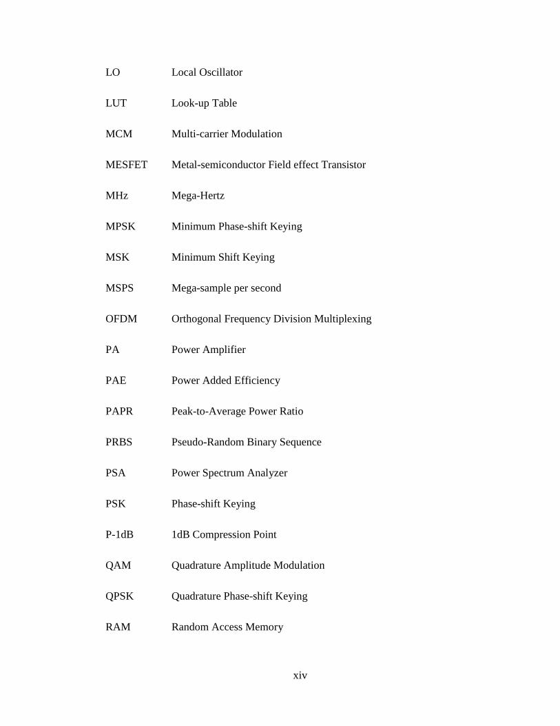
LO Local Oscillator
LUT Look-up Table
MCM Multi-carrier Modulation
MESFET Metal-semiconductor Field effect Transistor
MHz Mega-Hertz
MPSK Minimum Phase-shift Keying
MSK Minimum Shift Keying
MSPS Mega-sample per second
OFDM Orthogonal Frequency Division Multiplexing
PA Power Amplifier
PAE Power Added Efficiency
PAPR Peak-to-Average Power Ratio
PRBS Pseudo-Random Binary Sequence
PSA Power Spectrum Analyzer
PSK Phase-shift Keying
P-1dB 1dB Compression Point
QAM Quadrature Amplitude Modulation
QPSK Quadrature Phase-shift Keying
RAM Random Access Memory

xv
RF Radio Frequency
RMSE Root Mean Square Error
ROM Read-Only Memory
SDR Satellite Digital Radio
SSE Squared Sum of Error
TWTA Travelling Wave Tube Amplifier
VCO Voltage Controlled Oscillator
VHDL VHSIC hardware description language
1
1. INTRODUCTION
In 1992, the US Federal Communications Commission allocated a spectrum in
the „S-band‟ (2.3GHz) for nationwide broadcasting of satellite-based digital audio radio
service. Digital radio broadcast via satellite provided a means for delivering high
quality audio channels plus associated services to fixed and mobile receivers [1-4]. In
comparison with terrestrial broadcasts, the new satellite radio system now offers a
significantly wider geographical coverage at low cost and improved quality. Local
terrestrial links complement satellite coverage in major cities where tall buildings can
obstruct satellite signals from reaching the receivers. The satellite-terrestrial hybrid
systems have become a great success throughout North America, with Sirius XM
claiming over 18.5 million subscribers as of July 29, 2008 and becoming increasing
popular in other parts of the world. There is an ever–growing demand from car
manufacturers, mobile phone users and other portable device users. There is also a
potential growth as an alternative to existing terrestrial radio broadcasts provided it can
be made easily affordable by a bigger population. Currently, satellite radio uses the
2.3GHz (S-Band) in North America and generally shares the 1.4GHz (L-band) with
local Digital Audio Broadcasting (DAB) stations elsewhere.
2
1.1 Background of Research
1.1.1 Motivation
One of the main factors that can further increase the popularity of satellite radio
is reduced subscription cost. The major deciding factors regarding this are the capital
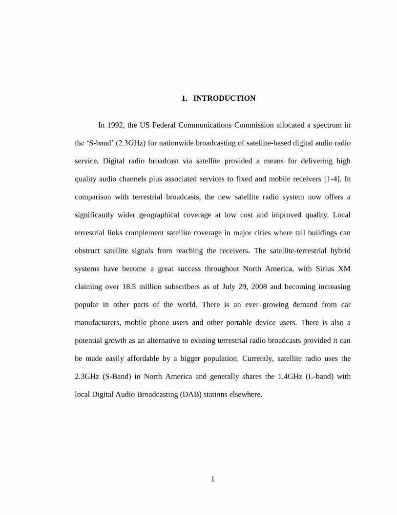
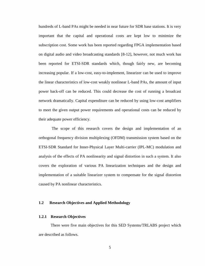
and operational costs incurred by service providers in running various satellite base
stations and broadcast networks as in Fig. 1.1.
Many of the newly developed standards for satellite radio such as the European
Telecommunications Standard Institute (ETSI) Satellite Digital Radio (SDR) are still
being developed and deployed. It is quite a challenging task to build a suitable hardware
platform that would have fast and intense processing capabilities, support high transfer
data rates, and at the same time be flexible and reprogrammable. Moreover, the
hardware complexity involved in such systems can raise the operational costs greatly.
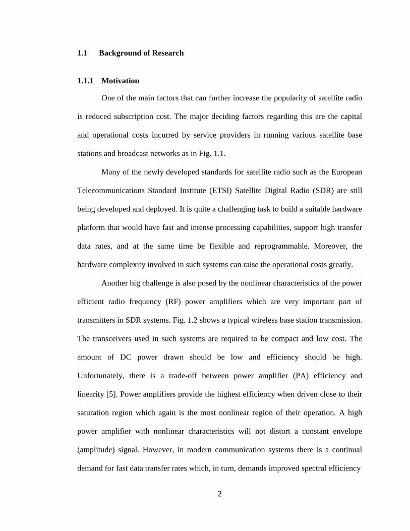
Another big challenge is also posed by the nonlinear characteristics of the power
efficient radio frequency (RF) power amplifiers which are very important part of
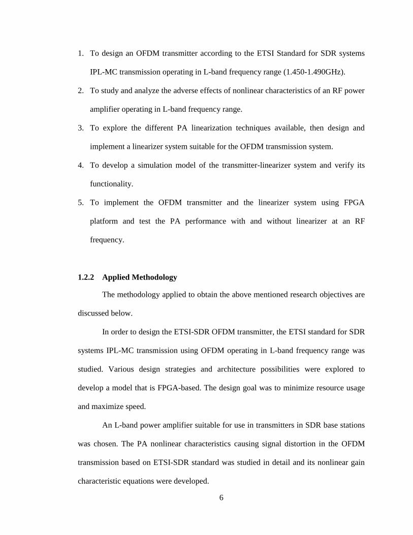
transmitters in SDR systems. Fig. 1.2 shows a typical wireless base station transmission.
The transceivers used in such systems are required to be compact and low cost. The
amount of DC power drawn should be low and efficiency should be high.
Unfortunately, there is a trade-off between power amplifier (PA) efficiency and
linearity [5]. Power amplifiers provide the highest efficiency when driven close to their
saturation region which again is the most nonlinear region of their operation. A high
power amplifier with nonlinear characteristics will not distort a constant envelope
(amplitude) signal. However, in modern communication systems there is a continual
demand for fast data transfer rates which, in turn, demands improved spectral efficiency
3
Figure 1.1 A typical Satellite Digital Radio broadcast network [2].
Figure 1.2 A typical wireless base-station transmitter.
using modulations schemes with increased Bits/Hz performance such as quadrature
amplitude modulation (QAM), quadrature phase-shift keying (QPSK) etc. Most of these
modulation schemes result in non-constant envelope signals, which when amplified by a
nonlinear PA, degrade the system performance and out-of-band power leakage causes
interference with systems operating in adjacent channels [6, 7].
4
Field programmable gate array (FPGA) devices provide a suitable, low-cost, off-
the-shelf development platform for various satellite radio standards. The fast processing
capabilities, vast logic resources, easy programmability and flexibility of FPGAs offer
an easy solution to the challenges faced in development and testing of new standards in
satellite radio based on software-defined radio concept. This reduces the hardware
implementation costs appreciably. Studies have been carried out over the years
regarding FPGA-based design and implementation of various wireless standards [8-12].
The introduction of FPGAs with fast digital signal processing (DSP) capabilities in the
recent years has revolutionized software-defined radio and a variety of state-of-the-art
design methodology has become available for design and implementation of complex
radio standards using FPGAs.
However, the challenge imposed by the PA nonlinear characteristics is very
complex. It is customary to back-off the operation region of high power amplifiers to
avoid the undesirable output signal distortion. A back-off of 6-9dB is common when
operating PAs. This means output power is only 12.5% to 25% of its maximum
resulting in an increase in operational costs. In some SDR-based systems, expensive
high power amplifiers with improved linearity can be used but this elevates the capital
expenses appreciably. Extending the linear region of operation of a weakly linear PA
and decreasing the input power back-off can potentially reduce the costs in SDR
systems.
1.1.2 Scope of Research
Satellite radio broadcast network is being deployed in various parts of the world
such as Europe, using the L-band frequency. There is a potential market where several
5
hundreds of L-band PAs might be needed in near future for SDR base stations. It is very
important that the capital and operational costs are kept low to minimize the
subscription cost. Some work has been reported regarding FPGA implementation based
on digital audio and video broadcasting standards [8-12], however, not much work has
been reported for ETSI-SDR standards which, though fairly new, are becoming
increasing popular. If a low-cost, easy-to-implement, linearizer can be used to improve
the linear characteristics of low-cost weakly nonlinear L-band PAs, the amount of input
power back-off can be reduced. This could decrease the cost of running a broadcast
network dramatically. Capital expenditure can be reduced by using low-cost amplifiers
to meet the given output power requirements and operational costs can be reduced by
their adequate power efficiency.
The scope of this research covers the design and implementation of an
orthogonal frequency division multiplexing (OFDM) transmission system based on the
ETSI-SDR Standard for Inner-Physical Layer Multi-carrier (IPL-MC) modulation and
analysis of the effects of PA nonlinearity and signal distortion in such a system. It also
covers the exploration of various PA linearization techniques and the design and
implementation of a suitable linearizer system to compensate for the signal distortion
caused by PA nonlinear characteristics.
1.2 Research Objectives and Applied Methodology
1.2.1 Research Objectives
There were five main objectives for this SED Systems/TRLABS project which
are described as follows.
6
1. To design an OFDM transmitter according to the ETSI Standard for SDR systems
IPL-MC transmission operating in L-band frequency range (1.450-1.490GHz).
2. To study and analyze the adverse effects of nonlinear characteristics of an RF power
amplifier operating in L-band frequency range.
3. To explore the different PA linearization techniques available, then design and
implement a linearizer system suitable for the OFDM transmission system.
4. To develop a simulation model of the transmitter-linearizer system and verify its
functionality.
5. To implement the OFDM transmitter and the linearizer system using FPGA
platform and test the PA performance with and without linearizer at an RF
frequency.
1.2.2 Applied Methodology
The methodology applied to obtain the above mentioned research objectives are
discussed below.
In order to design the ETSI-SDR OFDM transmitter, the ETSI standard for SDR
systems IPL-MC transmission using OFDM operating in L-band frequency range was
studied. Various design strategies and architecture possibilities were explored to
develop a model that is FPGA-based. The design goal was to minimize resource usage
and maximize speed.
An L-band power amplifier suitable for use in transmitters in SDR base stations
was chosen. The PA nonlinear characteristics causing signal distortion in the OFDM
transmission based on ETSI-SDR standard was studied in detail and its nonlinear gain
characteristic equations were developed.
7
A number of PA linearization techniques were explored to find a suitable
method of linearization of the L-band PA used in this research. The solution had to be
suitable for a signal bandwidth of 1.5314MHz, operable within L-band frequency range,
FPGA-implementable, low-cost and testable in hardware. An adaptive digital
predistortion based linearizer was designed for FPGA platform.
The PA performance in OFDM transmission with and without nonlinearity
compensation needed to be verified. A simulation test system was developed
comprising of simulation model of the ETSI-SDR OFDM transmitter, the simulation
model of the linearizer system and the simulation model of the L-band PA
experimentally obtained from gain and phase-shift characteristics. Simulations were
performed in an integrated environment of MATLAB, SIMULINK and Xilinx DSP
Development tools.
After simulation the design needed to be implemented and verified using FPGA
platform. This was achieved by setting up a hardware platform using FPGAs and
commercially available hardware. A suppression of spectral regrowth around 6-9dB
was expected from the hardware performance testing of the PA in OFDM transmission
after linearizer correction.
1.3 Thesis Outline
This thesis is organized into seven chapters. This first chapter introduces SDR
systems, its history, development and challenges which lead to the motivation for this
research and its goals.
8
Chapter 2 reviews the basic principles of OFDM transmission, which is very
popular in satellite radio standards. The RF power amplifier characteristics and their
effects resulting in signal distortion in OFDM transmission are also discussed.
Chapter 3 summarizes various techniques for PA linearization that has been
used in the past with special emphasis to the predistortion technique. A digital
predistortion based reference design was chosen as the reference for designing the
linearizer system to be used with the OFDM transmitter in this research to compensate
for the PA nonlinearity.
Chapter 4 discusses the methodology used in designing the FPGA-based ETSI-
SDR OFDM transmitter. A digital predistortion based linearizer system is also
described. This linearizer system was designed using a commercially available design
as reference.
Chapter 5 describes the simulation process. A simulation model of the L-band
PA used in this research was developed. Complete system integration was performed
using the simulation equivalent of the OFDM transmitter and the linearizer system, the
simulation model of the PA and other testing components. The functionality of the
OFDM transmitter and the PA nonlinearity effects were verified with and without
linearizer compensation, in simulation environment.
Chapter 6 provides details of the FPGA-based design and implementation of the
OFDM transmission system based on the ETSI-SDR standard specifications. The
linearizer implementation using FPGA and the hardware setup to test the system at an
RF frequency is also described. Finally, the results of hardware implementation of the
system are presented and discussed.
9
Chapter 7 presents a summary of results and conclusions with suggestions for
the future work.
1.4 Summary
This chapter introduces the SDR systems, its history, growth and challenges.
The motivation for this research, its scope and objectives are also introduced and the
outline of this thesis is discussed.
Satellite radio has attained immense popularity in North America during the past
decade and is also gaining popularity in Europe and the rest of the world. The principal
challenges in SDR-based systems are hardware complexity, demand for fast processing
capabilities and signal distortion caused by nonlinear characteristics of PA used in
transmitters. These factors increase the capital and operational costs substantially. This
research aims towards the design and implementation of an OFDM transmitter based on
satellite radio standard with PA nonlinearity compensation during OFDM transmission.
Next, in Chapter 2, the basic principles of an OFDM transmission system used
in satellite radio are reviewed and the effects of PA nonlinear characteristics resulting in
signal distortion are discussed.
10
2. OFDM TRANSMISSION AND SIGNAL DISTORTION
Recently, multi-carrier modulations (MCM) are receiving a lot of attention and
are being used in various SDR applications because of their many advantages over
single-carrier modulation schemes. OFDM is a type of MCM where adjacent
subcarriers are separated in frequency by the rate of the OFDM symbol to achieve
orthogonality between subcarriers. The various non-constant envelope modulation
schemes used in OFDM transmission for superior Bits/Hz performance produce signals
with variable amplitude. These signals are distorted when amplified by the nonlinear
power amplifiers used in base-station transreceivers.
The OFDM transmission principles, the various digital modulation schemes
used in OFDM and the distortion effects of PA nonlinearity on the transmitted signals
are discussed in this chapter.
2.1 OFDM Transmission
The basic principles of OFDM and the various digital modulation schemes used
in OFDM transmission is reviewed in the following subsections.
2.1.1 Basic Principles of OFDM Transmission
The fundamental principle of OFDM originated from Chang in 1966 [13]. The
serial data stream of a fast traffic channel is passed through a serial-to-parallel converter
11
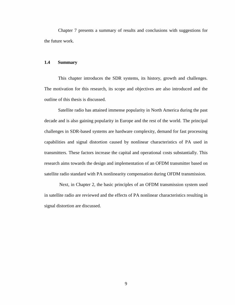
which splits the data into N number of slower rate parallel channels. The data in each
channel are applied to a modulator, such that, for N channels, there are N modulating
sub-carriers whose frequencies are f1, f2 f3 …. fN as shown in Fig. 2.1. The N modulated
carriers are then combined to give an OFDM signal. At the receiver, the OFDM signal
is de-multiplexed into N frequency bands and the N modulated signals are demodulated.
The baseband signals are then recombined using a parallel-to-serial converter.
The high data rate in such systems is achieved by splitting the data traffic into a
number of slower rate channels instead of using a high data rate single channel. The
orthogonality of sub-carriers allows overlapping without interference, thereby providing
better spectral efficiency. This feature makes OFDM a popular choice in satellite radio.
To avoid inter-symbol interference (ISI), a guard interval is inserted before each OFDM
symbol. The guard interval comprises of a sequence of all zero samples (zero-prefix) or
the last few samples of the OFDM symbol (cyclic-prefix).The cyclic-prefix insertion
results in the removal of intra-symbol interference by making the OFDM symbol appear
periodic.
The redundant samples from the guard interval are discarded at the receiver. The
main disadvantage of OFDM transmission is high peak-to-average-power-ratio (PAPR).
The PAPR of a signal is given as,
PAPR = Instantaneous peak value of a signal
Time averaged(root mean squared)value of the signal(2.1)
The superposition of a large number of sub-carriers in OFDM exhibit a high
instantaneous power with respect to average signal power resulting in PA saturation and
signal distortion.
12
Figure 2.1 OFDM modulator.
The data is usually digitally modulated and mapped to constellation before it is
available at the input of an OFDM modulator .The different types of digital modulation
schemes used in OFDM transmission are discussed in the following subsection.
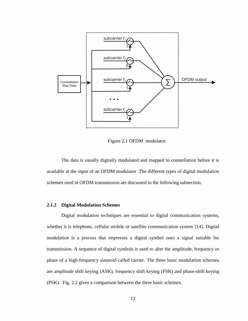
2.1.2 Digital Modulation Schemes
Digital modulation techniques are essential to digital communication systems,
whether it is telephone, cellular mobile or satellite communication system [14]. Digital
modulation is a process that impresses a digital symbol onto a signal suitable for
transmission. A sequence of digital symbols is used to alter the amplitude, frequency or
phase of a high-frequency sinusoid called carrier. The three basic modulation schemes
are amplitude shift keying (ASK), frequency shift keying (FSK) and phase-shift keying
(PSK). Fig. 2.2 gives a comparison between the three basic schemes.
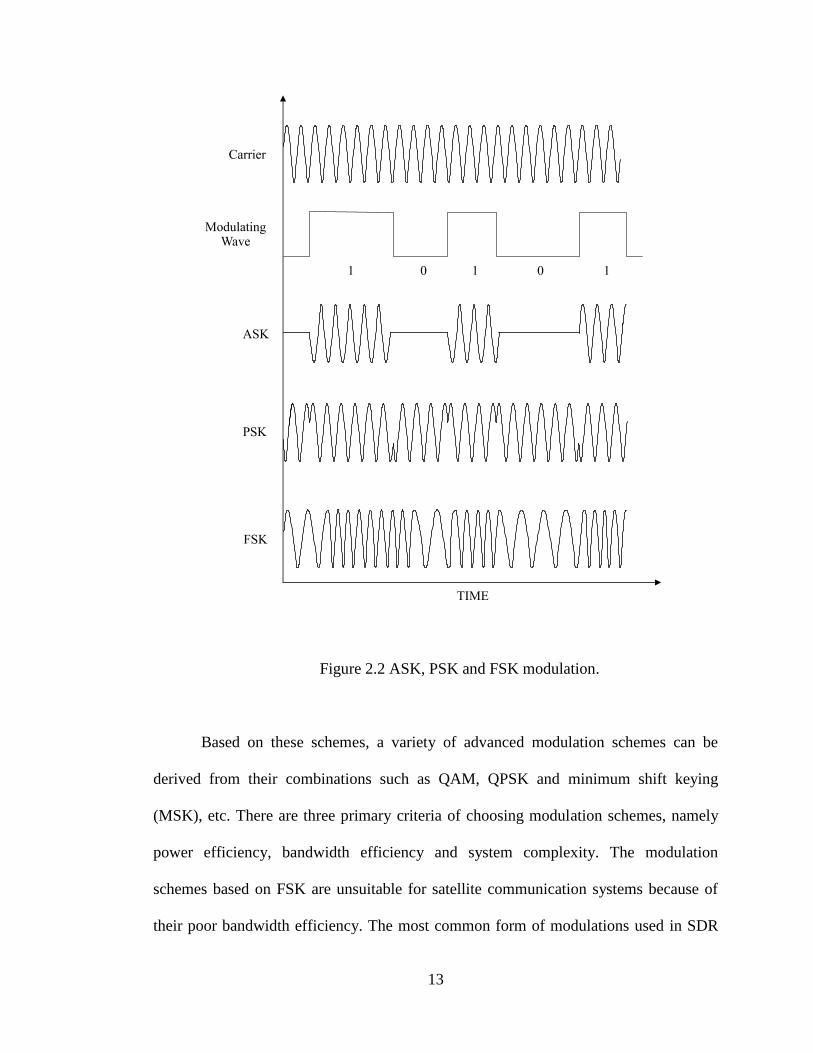
13
Figure 2.2 ASK, PSK and FSK modulation.
Based on these schemes, a variety of advanced modulation schemes can be
derived from their combinations such as QAM, QPSK and minimum shift keying
(MSK), etc. There are three primary criteria of choosing modulation schemes, namely
power efficiency, bandwidth efficiency and system complexity. The modulation
schemes based on FSK are unsuitable for satellite communication systems because of
their poor bandwidth efficiency. The most common form of modulations used in SDR
14
systems are QAM and QPSK. A k-bit M-ary QAM (M= 2 k ) is derived by modulating
both the amplitude and phase of an orthogonal carrier. For higher values of M, the
modulated signal provides a high bandwidth and power efficiency. The QPSK scheme
is derived by combining two bandwidth efficient binary PSK signals (BPSK), which is
also known as the 4-level M-ary PSK (M= 4). The signal constellation diagrams of a
16QAM and a QPSK are shown in Figures 2.3 and 2.4, respectively.
Filtering the digitally modulated data prior to transmission is required to band-
limit the modulated signal and to reduce inter-symbol interference (ISI) at the receiver.
The raised cosine filter has been widely used for this purpose. The raised cosine filter
can be approximated by filtering the modulated signal with analog filters or
equivalently by baseband pulse-shaping. This has been discussed in detail in [6] and [7].
These modulation schemes are broadly classified into two categories: constant
and non-constant envelopes. FSK, PSK and derived schemes such as QPSK, minimum
phase-shift keying (MPSK), etc. belong to the constant envelope category, while the
non-constant envelope modulation schemes are ASK, QAM, etc. In OFDM
transmission, since the orthogonality of the subcarriers must be maintained, not all types
of modulation schemes are suitable. QPSK and QAM are the most common choices
making them the most popular schemes used in SDR systems for OFDM transmission.
QAM uses amplitude modulation scheme, which always produces variable
envelope signal. A filtered QPSK scheme produces a fluctuating envelope signal as
well. The variable amplitude signals, when transmitted through efficient RF power
amplifiers, result in in-band signal distortion and out-of-band spectral leakage. The
effects of nonlinear characteristics of the PA on these signals are discussed next.

15
Figure 2.3 16QAM constellation.
Figure 2.4 QPSK constellation.
16
2.2 Power Amplifier Nonlinearity and Signal Distortion
The signal distortion in communication systems is attributed to the nonlinear
characteristics of its components such as RF power amplifiers. Therefore, it is critical to
study those characteristics and their effects. The following subsections discuss various
PA characteristics and their contribution to the in-band and out-of-band signal
distortion.
2.2.1 PA Efficiency vs. Linearity
There are two basic definitions of efficiency of a PA.
Drain Efficiency = RF output power
DC power consumed (2.2)
Power Added Efficiency (PAE) = RF output power - RF input power
DC power consumed (2.3)
The efficiency depends primarily on the output power and is virtually independent of
the signal bandwidth and PAPR. An amplifier is called linear if its gain is constant
throughout the range of the input signal. If this gain is not linear, the output signal is
distorted due to clipping and the amplifier is called nonlinear.
Amplifiers are commonly classified in four different classes, namely: A, B, AB
and C depending on their DC operating or bias points [5, 6]. The bias point is the most
important factor in determining the relationship between PA nonlinearity and
efficiency. Class A amplifiers, being biased in their linear region offer the highest

17
linearity as the transistors conduct over the entire RF cycle. However, they offer a very
poor power efficiency of only 50%. Class B amplifiers have no bias. Therefore the
transistors conduct only half the RF cycle and the output is high in harmonic distortion,
but they offer great improvement over Class A in terms of power efficiency. Class C
amplifiers are biased to conduct less than one half of RF cycle and therefore, offer up to
100% efficiency theoretically as the conduction angle approaches zero. However, they
are highly nonlinear. The class AB amplifiers offer better efficiency than Class B as
their transistors conduct for more than half of RF cycle and their minimal DC bias is
just sufficient to overcome cross-over. The improved efficiency and weak nonlinearity
have made Class AB amplifiers a popular choice in communication systems.
2.2.2 PA Nonlinear Characteristics
In an ideal PA with linear gain A and phase constant Φ, the complex transfer
function is independent of the amplifier input level and is given by,
jAeG (2.4)
In case of a real amplifier, however, the gain A(s(t)) and phase-shift Φ(s(t)) are
functions of the input signal s(t) and the complex transfer function is dependent on
amplifier input power and is given by,
))(())(())(( tsjetsAtsG
(2.5)
Therefore, in a real amplifier, gain decreases and phase-shift changes as the level of
input signal drives the amplifier in its saturation region. The output amplitude and phase
characteristics are known as AM-AM characteristics and AM-PM characteristics,
18
respectively. The AM-AM and AM-PM characteristics of an ideal PA vs. typical
nonlinear PA are shown in Figures 2.5 (a) and (b), respectively.
In digital communication systems, it is possible to obtain the AM-AM and AM-
PM characteristics as a function of complex input signal sample as in [15] and [16]. For
an nth
complex input sample zn with a magnitude | zn | and a phase arg(zn), the complex
transfer function of the nonlinear PA is given by,
)(arg2 2
)()( nn zPMzj
nn ezAMzA
(2.6)
where AM (|zn|2) and PM (|zn|
2) are polynomial functions derived from the AM-AM and
AM-PM characteristics, respectively and |zn|2 is the power of the n
th complex input
sample. Considering the nonlinear PA without memory, AM-AM and AM-PM
characteristics are sufficient to model the PA behavior. The complex transfer function
takes the form,
k
n
N
k
nkn zzazA2
1
0
)(
(2.7)
where, N gives the number of polynomial terms and ak is the kth
polynomial
coefficient.
For wideband signals, usually memory effects cannot be ignored for practical
purposes. In such cases simplified versions of the Volterra or the Wiener-Hammerstein
system of modeling are used. And the complex transfer function is modeled as a
polynomial function of current and previous complex input signal samples. Detailed
discussion of this type of PA modeling with references can be found in [16].
19
Figure 2.5(a) AM-AM characteristics.
Figure 2.5(b) AM-PM characteristics.
Nonlinearity of a PA is measured by various factors such as 1dB compression
point, third order intercept point (IP3) and adjacent channel power ratio (ACPR) and
harmonics. The 1dB compression point (P-1dB) gives the input signal level that causes
20
the gain to drop by 1dB from its small signal value. The third order intercept point (IP3)
is a purely mathematical measure of nonlinearity and has no practical use in the
physical world. It is defined as the input level at which the output distortion power
increases by three times that of the increase in carrier power. Adjacent channel power
ratio is of practical significance and is given by,
ACPR =
Total power in adjacent channel
Power in the main channel (2.8)
The following section provides a brief overview of constant and non-constant signal
envelope modulation schemes and signal distortion.
2.2.3 Intermodulation Distortion and Spectral Regrowth
When a constant envelope signal, such as the one with amplitude V and a single
tone f given by Vcos(2πft), is transmitted through a nonlinear PA, the output signal
spectrum will have component at f as well as harmonic distortion components at ±2f,
±3f, etc. These components can be easily filtered out and, as such, pose no problem.
However, when a non-constant envelope signal is transmitted through a nonlinear PA,
the output signal spectrum consists of harmonic components and as well as distortion
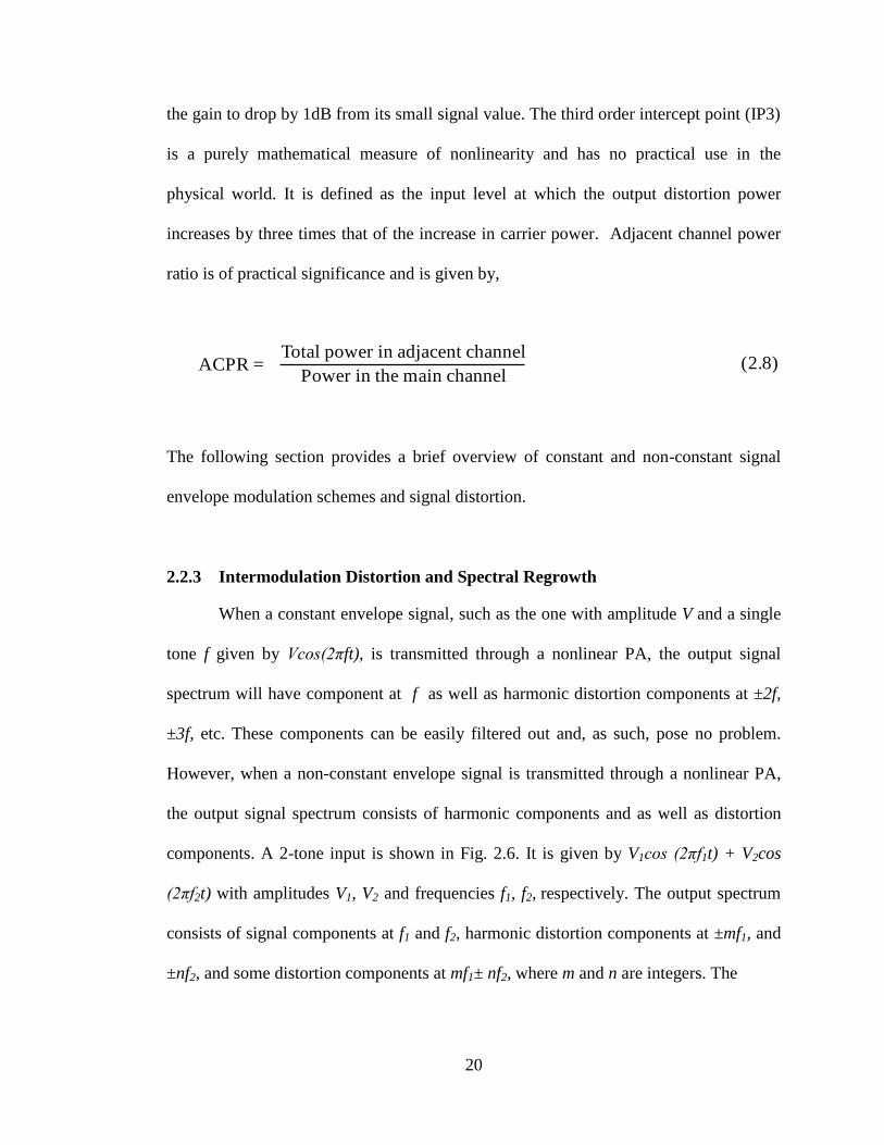
components. A 2-tone input is shown in Fig. 2.6. It is given by V1cos (2πf1t) + V2cos
(2πf2t) with amplitudes V1, V2 and frequencies f1, f2, respectively. The output spectrum
consists of signal components at f1 and f2, harmonic distortion components at ±mf1, and
±nf2, and some distortion components at mf1± nf2, where m and n are integers. The
21
Figure 2.6 Intermodulation distortion products of a 2-tone signal.
components at mf1± nf2 frequencies cause output signal distortion called intermodulation
distortion (IMD) and the components are known as IMD products. The third order IMD
products at 2f1- f2 and 2f2- f1 are especially troublesome because they fall within the
transmission pass-band of the PA and cannot be removed by filtering.
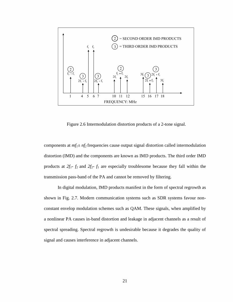
In digital modulation, IMD products manifest in the form of spectral regrowth as
shown in Fig. 2.7. Modern communication systems such as SDR systems favour non-
constant envelop modulation schemes such as QAM. These signals, when amplified by
a nonlinear PA causes in-band distortion and leakage in adjacent channels as a result of
spectral spreading. Spectral regrowth is undesirable because it degrades the quality of
signal and causes interference in adjacent channels.
22
Figure 2.7 Spectral regrowth in digital modulation.
2.3 Summary
OFDM transmission, which is very popular in satellite radio standards, has been
discussed in this chapter. The basic principles of OFDM transmission and the various
digital modulation schemes available have been reviewed. Modulation schemes such as
QAM and QPSK are suitable for OFDM transmission because of the orthogonality of
the carriers. However, they result in fluctuating envelope signals. The variable envelope
signals, while transmission, undergo distortion in the form of spectral regrowth when
they drive the transmitting RF power amplifiers to the nonlinear region of operation of
the latter.
The various PA characteristics have also been discussed in this chapter with
special emphasis on their nonlinear characteristics. The effects of PA nonlinearity on
the non-constant envelope signals were presented. The complex transfer function of the

23
PA at an instant is dependent on the instantaneous input power. Therefore, the nonlinear
characteristics of a PA can be expressed as a function of amplitude and phase of the
input signal. Constant envelope signals produce harmonic distortion components when
transmitted by a nonlinear PA, which can be easily eliminated by filtering. However,
non-constant envelope modulation schemes produce distortion components as well as
harmonic components, which cannot be removed by filtering. They manifest in the form
of spectral regrowth in digital communication systems.
The next chapter provides a brief review of various PA linearization techniques
that have used over the years and discusses the choice of a linearization method to be
used in this research.
24
3. LINEARIZATION TECHNIQUES
The trade-off between efficiency and linearity cannot be denied in RF power
amplifiers. Whether efficiency or nonlinearity is of primary concern, depends on the
nature of the application. There is no one particular solution that fits the problem. The
portable communication devices need longer battery life time and efficiency is a major
concern. On the other hand, linearity of the PA used at the base station equipments is
the primary concern in satellite communications systems. In such applications,
efficiency is important but secondary consideration [17]. This research focuses on low-
cost weakly nonlinear L-band PA that can be used in base station equipment in satellite
radio to reduce capital and operational costs. Therefore, various PA linearization
techniques are explored.
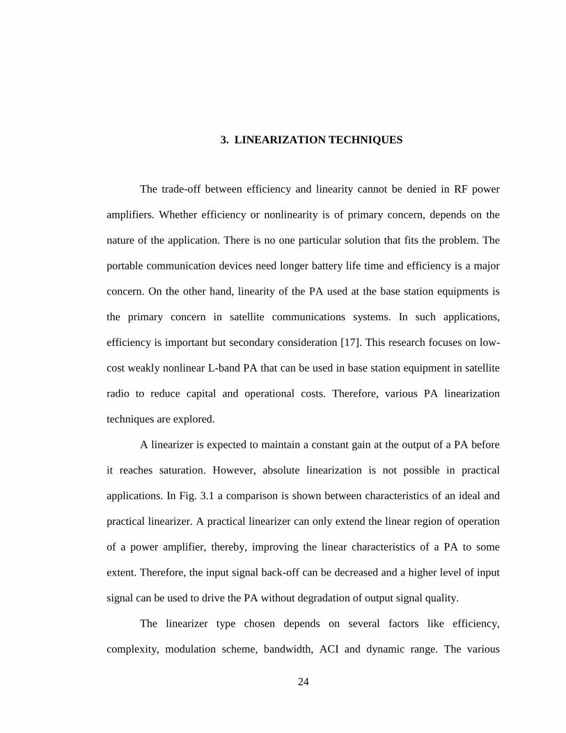
A linearizer is expected to maintain a constant gain at the output of a PA before
it reaches saturation. However, absolute linearization is not possible in practical
applications. In Fig. 3.1 a comparison is shown between characteristics of an ideal and
practical linearizer. A practical linearizer can only extend the linear region of operation
of a power amplifier, thereby, improving the linear characteristics of a PA to some
extent. Therefore, the input signal back-off can be decreased and a higher level of input
signal can be used to drive the PA without degradation of output signal quality.
The linearizer type chosen depends on several factors like efficiency,
complexity, modulation scheme, bandwidth, ACI and dynamic range. The various
25
Figure 3.1 Effect of linearizer on PA output.
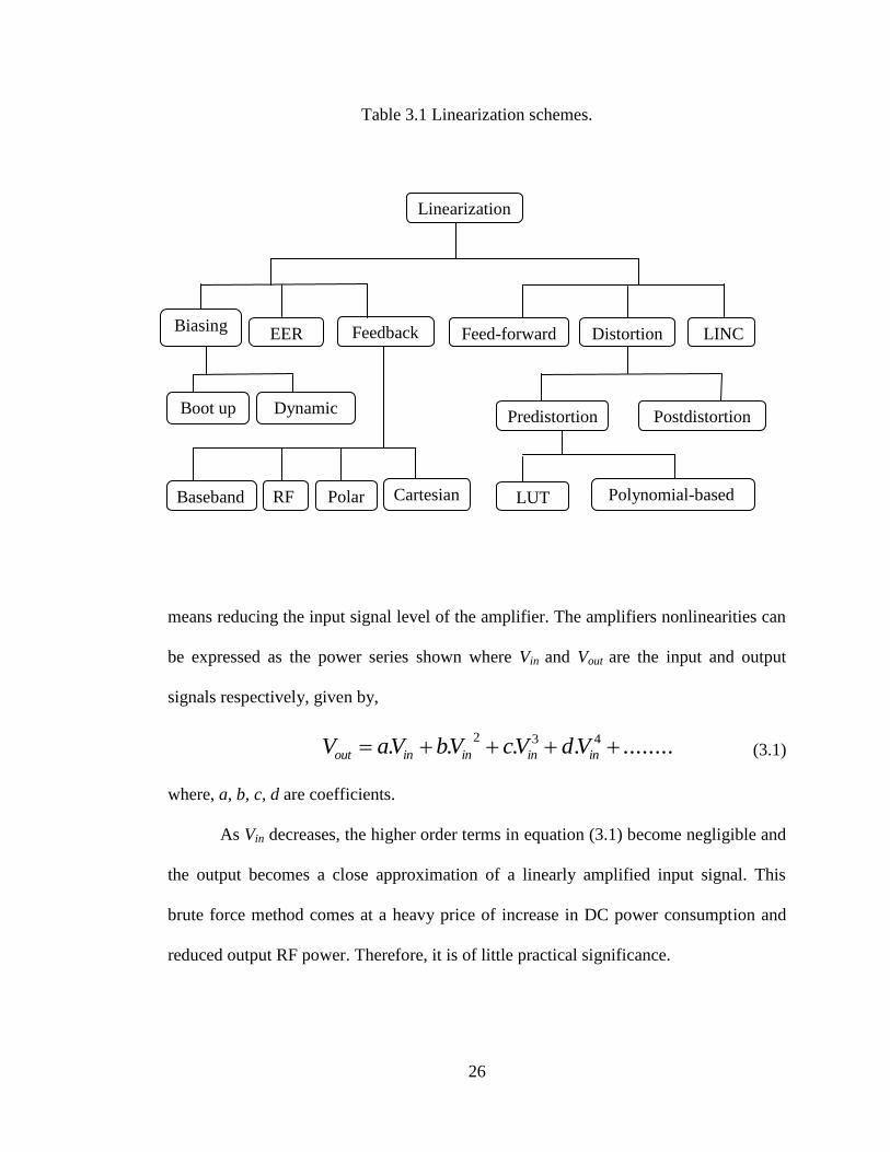
schemes are classified based on their functionality, architecture, application etc. Some
commonly used linearization schemes are given by Table 3.1 and discussed in
subsequent sections.
3.1 Biasing Methods
The DC bias level or bias point of amplifiers directly affects their linearity and
power efficiency as discussed in Section 2.2 of Chapter 2. The biasing method of
linearization involves extending the linear region of operation of a PA by changing its
DC bias level. The different biasing methods are discussed in the following subsections.
3.1.1 Boot up Bias
The simplest and most obvious way to improve the linearity of a PA is to
increase the bias levels and driving it towards Class A region of operation [18]. This
26
Linearization
Biasing Feed-forward
Dynamic
Distortion LINC Feedback
Boot up
EER
Baseband RF Polar Cartesian
Predistortion Postdistortion
LUT
based
Polynomial-based
Table 3.1 Linearization schemes.
means reducing the input signal level of the amplifier. The amplifiers nonlinearities can
be expressed as the power series shown where Vin and Vout are the input and output
signals respectively, given by,
............. 432
ininininout VdVcVbVaV (3.1)
where, a, b, c, d are coefficients.
As Vin decreases, the higher order terms in equation (3.1) become negligible and
the output becomes a close approximation of a linearly amplified input signal. This
brute force method comes at a heavy price of increase in DC power consumption and
reduced output RF power. Therefore, it is of little practical significance.
27
3.1.2 Dynamic Bias
Increasing bias to linearize an amplifier is not a good choice but increasing the
bias adaptively only during times of need is a comparatively better choice [18]. The bias
levels are adjusted such that the amplifier uses as little power as possible while staying
within distortion tolerances. Figure 3.2(a) shows one such bias circuit implementation.
As the input level is increased; the bias level is also increase adaptively, thereby forcing
the amplifier to operate in its linear region. A linear amplifier‟s 1dB compression region
can be pushed up by a few dB using this method.
An improvement made to this circuit is Figure 3.2(b). The idea is to set the
attenuation such that it is just equal to the small signal gain of the power amplifier with
the bias set very low. As the input signal starts to increase into the gain compression
region of the PA, the gain of the PA starts to decrease. This gain decrease is sensed by
the op-amp and the bias level is increased to compensate. Thus, efficiency can be
improved and the output can be linearized.
Unfortunately, this method requires a very high speed envelope detector and a
DC-DC converter with a high current capability which can be quite challenging.
Another drawback lies in the fact that for large changes in the bias levels, undesired
phase-shift occurs. Therefore, the improvement achieved by envelope correction can be
corrupted by phase distortion. Attempt to correct this with a phase feedback loop
increases undesired design complexity in RF applications.
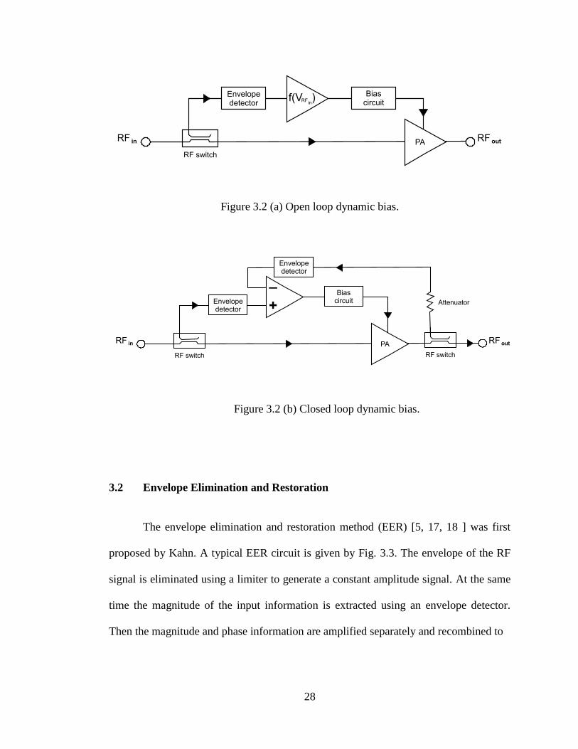
28
Figure 3.2 (a) Open loop dynamic bias.
Figure 3.2 (b) Closed loop dynamic bias.
3.2 Envelope Elimination and Restoration
The envelope elimination and restoration method (EER) [5, 17, 18 ] was first
proposed by Kahn. A typical EER circuit is given by Fig. 3.3. The envelope of the RF
signal is eliminated using a limiter to generate a constant amplitude signal. At the same
time the magnitude of the input information is extracted using an envelope detector.
Then the magnitude and phase information are amplified separately and recombined to

29
Figure 3.3 Envelope elimination and restoration.
restore the desired RF output. The magnitude and phase information can be combined
by using a switch-mode RF power amplifier.
The envelope is restored by driving the bias supply of the RF power amplifier
with the original envelope. Theoretically, this method can provide 100% power
efficiency since the PA is operated nonlinearly in a switched mode. Unlike several
linearization schemes which can only improve the performance of a weakly nonlinear
PA, the EER method can be used to compensate for a completely nonlinear PA.
A disadvantage of this method is that envelope restoration is performed by
biasing the drain voltage of the amplifier. As the drain voltage is varied to correct the
output amplitude of the PA, there is some variation in phase also. If this phase variation
increases beyond the tolerance level, it contributes to spectral regrowth. Another typical
disadvantage is the slowness of the envelope restoration feedback loop.

30
3.3 Feedback Methods
3.3.1 RF Feedback
Another simple form of linearization is to use the direct RF feedback technique
using the principle of operational amplifiers [17, 18]. In this technique, as shown in Fig.
3.4, there is a feedback circuit which subtracts a voltage βVout from the input signal Vin
and the composite gain is given by,
A
AG
1 (3.2)
where A is the amplifier gain. The idea is to desensitize G to any variation in A by
application of feedback gain β.
The main drawback of this system is that it assumes that the feedback
occurs simultaneously. However, a typical RF amplifier is made up of many cascaded
stages to get enough gain. A single stage can have a time delay of several RF cycles.
This time delay effect causes instability in the system.
3.3.2 Baseband feedback
Baseband feedback method [18] reduces the bandwidth required by the feedback
loop by feeding back the baseband signal instead of the RF signal as in Fig. 3.5. The
baseband signal is modulated onto the RF carrier and amplified by the PA at RF
frequency, then the output is demodulated and fed back to adjust the input given to the
high gain base band amplifier so that the output of the RF power amplifier is linearized.
It is assumed that the demodulator is linear and distortion free at the bandwidth of
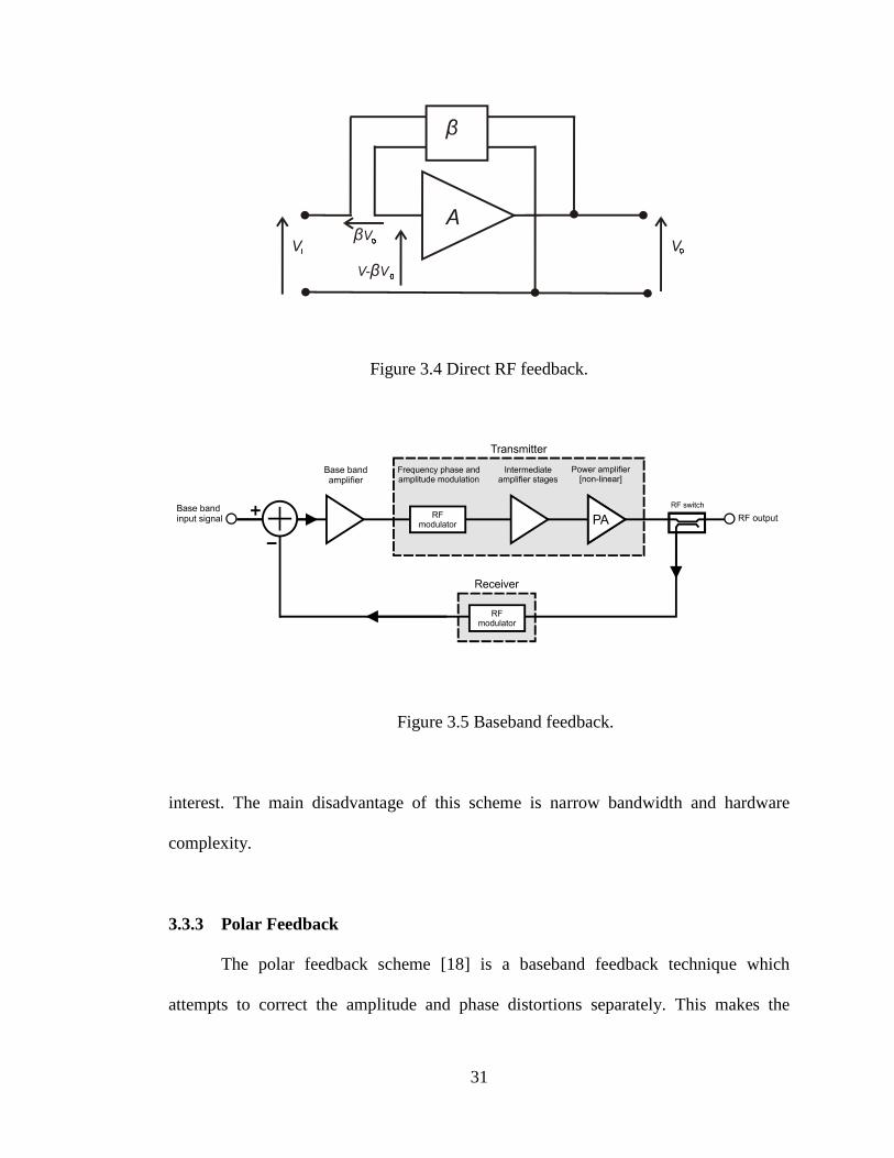
31
Figure 3.4 Direct RF feedback.
Figure 3.5 Baseband feedback.
interest. The main disadvantage of this scheme is narrow bandwidth and hardware
complexity.
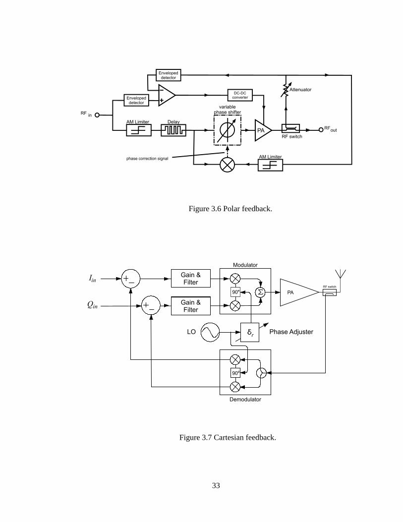
3.3.3 Polar Feedback
The polar feedback scheme [18] is a baseband feedback technique which
attempts to correct the amplitude and phase distortions separately. This makes the

32
system quite robust. Figure 3.6 shows a typical polar feedback circuit. Since both
amplitude and phase are corrected in the polar feedback system; variations in
temperature, load and manufacturing should be mitigated.
The most severe disadvantage of this system is that matching the delays of the
amplitude and phase feedback paths, which is non-trivial. Another key disadvantage is
different bandwidth requirements for envelope and phase feedback paths. The phase
bandwidth needs to higher than the envelope bandwidth. Depending on application this
might lead to poor overall performance in terms of correction of distortion. Also this
puts severe limitations on bandwidth and its usefulness is limited to single-carrier
applications only.
3.3.4 Cartesian Feedback
Cartesian Feedback method [5, 7, 17, 18], first proposed by Petrovic, offers
some advantages over the polar feedback method. Figure 3.7 shows the baseband input
signal is fed to the error correcting differential amplifiers, filtered and used to I-Q
modulate the RF carrier. The modulated signal is amplifier by the RF power amplifier
and the distorted output signal emerges. A small portion of this distorted signal is
demodulated, fed back and compared with the input undistorted baseband signals.
Synchronization between the modulator and demodulator is obtained by splitting the
common carrier signal. The gain of the input differential amplifiers forces the loop into
generating an output signal that closely resembles the original signal.
33
Figure 3.6 Polar feedback.
Figure 3.7 Cartesian feedback.

34
One of the benefits of this method over the polar method is that there is
asymmetry between the gain and bandwidth in the two quadrature signal processing
paths. This reduces the tendency to introduce phase-shifts between AM-AM and AM-
PM processes. The overall system is simple and attractive but there are bandwidth
restrictions imposed by baseband signal processing. Also the feedback loop is prone to
stability issues as the RF amplifier creates a phase-shift that changes with frequency. A
phase-shifter is used to maintain the correct relationship between the input signals and
feedback signals. Another limiting factor is the nonlinearities in the down converting
mixer.
3.4 Feed-forward Method
Feed-forward is an old linearization technique [7, 17, 18 ] invented by Black in
1923 to linearize telephone repeaters. It has been used since then and has successfully
linearized many PAs. Figure 3.8 shows a feed-forward-based linearization circuit. The
basic difference between feed-forward and feedback methods is that the correction is
applied to the output signal in the former unlike in the latter scheme. A non-distorted
input signal is fed to the main PA as well as to a variable gain/phase amplifier in
Canceller #1. A delayed sample of the input is compared with the coupled and suitably
attenuated output signal. The adaptive system samples the power at point “A” and
adjusts the gain and phase of Canceller #1 such that the power at “A” is minimized.
When the power is minimized, only the distortion from the PA remains at point “A”.
This distortion then passes through Canceller #2 which adaptively adjusts its gain and

35
Figure 3.8 Feed-forward scheme.
phase to minimize the total power at point “B”. The only way to achieve this is by
cancelling the distortion from the PA.
There are some advantages to this method. This method corrects in-band
amplitude and phase distortion without the instability issues of feedback systems.
However, the success of this method is based on a few assumptions. First of all, it
assumes that the PA generates the dominant nonlinearity. It also assumes that the
distortion components are small compared to the desired signal. The method usually
works well at one frequency and not so adaptive to change in amplifier characteristics
because of time, temperature variations etc. This method also comes at a price that the
correction signals need to be amplifier to the necessary higher power level.
3.5 Linear Amplification with Nonlinear Components
Linear amplification with nonlinear components (LINC) [5, 7] is a technique
that uses nonlinear amplifiers for linearization as shown in Fig. 3.9. It is based on the

36
Figure 3.9 LINC system.
principle that a band pass signal Vin(t) can be expressed as the sum of two constant
amplitude phase modulated signals V1(t) and V2(t) given by,
)]()(cos[)()( tttrtV cin (3.3)
)]()()(sin[
2)(1 ttt
KtV c
(3.4)
)]()()(sin[2
)(2 tttK
tV c (3.5)
where, r(t)ejθ(t)
is the complex envelope of the band pass signal, ωc is the carrier
frequency, K ≥ max r(t) and Ψ(t) = sin-1
[r(t)/K].
V1(t) and V2(t) are separately amplified by two separate nonlinear amplifiers and
the output can be combined to produce Vin(t). A feedback mechanism can be added to
correct any mismatch between amplifiers. The problem with this method is it requires
two separate PAs and a low loss combining circuit to combine the outputs.
37
3.6 Distortion Methods
Distortion methods involve linearization by distorting the signal to compensate
for amplifier nonlinearities. Predistortion involving distorting the input signal before
amplification is more common than postdistortion method involving distortion of the
output signal.
3.6.1 Postdistortion
There have been some reports regarding cancellation of PA nonlinearities by
postdistortion in the receiver [19-21]. The basic principle is to use a linearizer circuit to
distort the amplified received signal to cancel the effects of the distortion introduced by
the PA nonlinearity. Figure 3.10 shows a basic postdistortion linearizer circuit. The
postdistorter generates a nonlinear distortion signal based on the envelope of the
received signal such that the third and fifth order IMD products can be cancelled. The
third and fifth order IMD products are the main concern because they are within the
bandwidth of interest and cannot be filter out. Upon combining the amplified and the
post distorted signals, IMD products of the resulting signal are reduced.
Two different methods have been discussed in [19] and [20]. The “power-based”
method requires the center channel idling while the postdistorter adapts, while the
“variance-based” method uses the variance of the received samples as an indication of
ACI power and the predistorter adapts accordingly. A digital postdistorter lineraizer is
implemented in [21] using ROM-based look-up tables to cancel the 3rd
and 5th
order
IMD products.
38
Figure 3.10 A simplified postdistortion linearizer circuit.
Postdistortion method has failed to attain popularity because linearizing a high
power signal is not attractive because it hurts the overall efficiency of the system. Also
receiver postdistortion does not provide a solution for the spectral spreading.
3.6.2 Predistortion
Predistortion is arguably one of the most popular linearization schemes because
it offers an inexpensive solution at a great bandwidth. A nonlinear circuit is inserted
between the input signal and the PA. This nonlinear circuit generates the IMD products
inverse to those produced by the PA and thereby cancelling the effect of PA
nonlinearity. Predistortion can be implemented at baseband, intermediate frequency (IF)
or radio frequency (RF) making it quite versatile. The adaptation of the predistorter is
achieved by feedback. Unlike the feedback techniques, this feedback is not used for real
time calculation of the predistorted signal. Thus the predistortion based linearizer is
insensitive to loop delay and more stable. There has been a reasonable amount of
research carried out in this area [6, 7, 22-31]. Mostly, predistortion has been used in the
region immediately below the 1dB compression point of the PA characteristics. Figure
39
3.11 shows a simplified predistortion circuit. The methods mostly differ in the design
and implementation of the nonlinear predistorter. These can be broadly classified into
LUT-based and polynomial-based predistorters and described below.
LUT-based predistorter: The LUT based predistorter is typically implemented at
the baseband. The LUT is either mapping type or gain-based. In the mapping type of
predistorter, the LUT is stored in RAM and contains the predistortion value appropriate
for any complex input signal sample. The value of the complex sample is used to
address the appropriate predistortion values. Implementation problems include long
LUTs and reported instability in the feedback loop which requires a phase-shifter.
The gain-based predistorter implements a LUT of complex gain values as a
function of input power envelope. When combined with the complex gain values of the
amplifier, a constant gain for any input level results. This method requires less memory
and no phase-shifter in the feedback path.
Polynomial-based predistorter: Another class of predistorter uses polynomial
functions to generate predistortion. This type is typically implemented in IF or RF. The
inverse nonlinear characteristics of a PA are generated using predistorter of variable
gain and phase. This method usually corrects the 3rd
and 5th
order IMD products, but
linearization up to the 7th
order has been proposed by Ghaderi [7]. The main drawback
of this method is hardware complexity by using analog predistorter for the polynomials.
The analog polynomial is generated using a series of analog multipliers and analog level
detector is used for envelope detection [6]. This ultimately increases the cost of
implementation.
40
Figure 3.11 A simplified predistortion linearizer circuit.
3.7 Digital Predistortion
Predistortion can be easily applied to signals in digital domain using fast
commercially available DSP processors. The baseband signals can be analog or digital
data. A digital predistorter can operate at baseband, IF or RF. It is more flexible and
therefore more suitable for commercial applications than its analog counterpart. The
enhanced correction and adaptation capability has made it popular in the modern
communications industry. However, the DSP algorithms that achieve this performance
are very processor-intensive. In application-specific integrated circuit (ASIC)
implementation, this requires very large ASICs which must be able to cope with many
different amplifiers and topologies to address the broadest market. This also makes the
ASIC more complex and power-hungry. Thus, an FPGA-based solution is preferred.
Using FPGA-based digital predistortion, the flexibility of the device allows the
implementation of a specific algorithm for a specific amplifier being predistorted. The
processor does not have to be overly complex, hence it reduces silicon space and can be
cost-effective. Although, many versions of the digital pre-distorters have been
developed in past several years, the most popular ones are LUT-based or parametric
41
predistorter with an analytical formulation (such as Volterra kernel-based predistorter).
These LUT-based digital predistorters are preferred because of bandwidth flexibility,
low cost and reduced hardware-software complexity.
One of the principal objectives of this research was to design a suitable
linearizer for an RF power amplifier which would be inexpensive and easily
implementable using FPGAs. A commercially available state-of-the-art reference
design from Xilinx [32-34] was used as the basis for this design. The design uses LUT-
based predistortion algorithm and the envelope of the complex input sample is used for
LUT-indexing. The entire design can be contained in a suitable Xilinx FPGA. The
design is hardware-software co-design and the entire predistortion coefficient
estimation is computed in the software, thereby saving FPGA resources. The design has
been reported [32-34] to have improved up to 15-25dB reduction in spectral regrowth
for certain wideband standards with considerable crest factor reduction (CFR). It also
provides quadarature modulator gain imperfection corrections. Clearly, the Xilinx
reference design offers several advantages and therefore was chosen for this research.
3.8 Summary
This chapter reviews the various techniques that have been used in the past for
PA linearization in communication systems. The linearization methods were explored
and their various advantages and disadvantages were compared. Digital predistortion
method of linearization was found most suitable because of reduced hardware
complexity, low cost and easy implementation.

42
A commercially available reference design from Xilinx was chosen as the basis
for designing a digital predistortion-based linearizer system for this research. This DPD
linearizer is a hardware-software co-design which can be easily implemented using a
Xilinx FPGA. The performance testing reports of the linearizer show a significant
amount of spectral regrowth suppression is possible.
In the next chapter, the methodology used in designing the ETSI-SDR OFDM
transmission system and the linearizer system is discussed.
43
4. DESIGN OF TRANSMITTER AND LINEARIZER
The design and implementation of various digital communication standards
using software defined radio concept are gaining popularity with the rapid advancement
in the field of digital signal processing. In this chapter, the design of an OFDM
transmission system based on standard ETSI TS 102 551-2 V2.1.1 (2007-2008) for
satellite radio is described in detail starting from data generation to OFDM modulation.
Also, a linearizer system is designed to be used to compensate for the nonlinear
characteristics of the RF power amplifier in the base station transreceiver system. A
digital predistortion-based linearizer reference design from Xilinx [35] was used as
reference to design the linearizer system. Both designs are targeted for implementation
using Xilinx FPGAs for DSP design.
4.1 Design of OFDM Transmitter
4.1.1 ETSI TS 102 551-2 V2.1.1 (2007-2008)
Modern digital communications favour OFDM systems because of their various
advantages such as spectral efficiency, reduced inter-symbol interference (ISI) and
flexibility of deployment across various frequency bands with little modification to the
air interface. The ETSI radio interface standard, ETSI TS 102 551-2 V2.1.1 (2007-08)
[36] for IPL-MC transmission using OFDM is used in this research. The mode of

44
interest is Mode-3 with OFDM at 1k (i.e. 1024 FFT length) with 1.7MHz channel
spacing. The specifications obtained from this mode have been used as a reference to
model a fixed-point, FPGA-based OFDM system. The signal constellation used is gray
coded 16-QAM. The OFDM parameters in ETSI TS 102 551-2 V2.1.1 (2007-08)
Mode-3 are listed in Table 4.1.
4.1.2 Data Generation and OFDM transmission
The process of designing the OFDM system model included two steps. The first
step was to develop and test the model structure in floating point using MATLAB
version R2007a [37]. The output was verified and analyzed. The next step was to
develop a fixed point equivalent of the model that would be suitable to be contained
completely in an FPGA. Figure 4.1 shows the necessary steps starting from data
generation to the OFDM output samples. The graphical design environment chosen was
Xilinx System Generator 10.1 [38] for Windows XP SP3 which is a DSP design tool
from Xilinx. For the purpose of this research a sample based input instead of a frame
based input was sufficient, therefore generation of preamble was not required. The
Xilinx System Generator design flow can be divided into four subsections, namely:
Random data generation, mapping to constellation, pilot generation, interleaving and
pulse shaping of data, OFDM generation and cyclic prefix adding.
The first component in the transmitter design is a random data generator. This
module uses Xilinx linear feedback shift register (LFSR) IP cores [39]. Each LFSR
generates a pseudo random binary sequence (PRBS). Four Galois-type LFSRs having
45
Table 4.1 ETSI TS 102 551-2 Mode-3 OFDM parameters [36].
Parameter Unit Value
Modulation index -- 4
FFT length -- 1024
Active subcarriers -- 729
Guard interval ratio -- 1/4
Sampling frequency MHz 2.1511
Pilots per OFDM symbol -- 127
Sub-carrier distance KHz 2.1000
Signal Bandwidth MHz 1.5314
Figure 4.1 OFDM modulation based on ETSI standard.
20, 21, 17 and 18 bits were used in parallel to maximize the PRBS sequence as
described in Appendix A. Two-input exclusive-OR (XOR) gates were used for feedback
taps. The generated sequence was of length 2LFSR-SIZE
-1. An autocorrelation function
was used in MATLAB on the generated sequence to determine their random nature.
46
Autocorrelation Rxx(j) [40] of a generated discrete sequence xn is defined as the
correlation between its samples when a time-lag is applied to them. The autocorrelation
of a discrete sequence at time-lag j is given by,
*)()(
n
jnnxx xxjR (4.1)
where, (xn)* is the complex-conjugate of xn. Figure 4.2 shows the autocorrelation of the
generated sequence for j from 0 to 20.
The next step was mapping the symbols to the constellation. The mapping
scheme chosen was non-hierarchical 16QAM with gray coding as in Fig. 4.3. This part
of the design could be realized using various options. To maintain design simplicity and
minimize resource usage, advantage was taken of the unique feature of Xilinx System
Generator that allows simple MATLAB codes to be imported into the design
environment. This was achieved by using Xilinx M-code design block while
maintaining the fixed point representation of the data. The 4-bit output of the random
data generator was treated as an input symbol in the frequency domain and was mapped
to 16QAM constellation. The output was obtained in the form of I/Q pairs. The average
power of the various M-ary QAM modulated signals was required to be normalized to
unity before transmission. This involved the normalization of the power level of I/Q
output pairs by multiplication by a factor of 101 [36]. The hardware multipliers
available on FPGAs use significant amount of logic resources and introduce round-off
noise in the system because they allow multiplication by powers of 2. Therefore, the M-
code block used in the 16QAM Mapper was also used to perform the normalization
using MATLAB functions. This allowed increased precision and eliminated the need
for hardware multipliers.
47
Figure 4.2 Autocorrelation of input data samples.
Figure 4.3 Gray coded 16QAM constellation.
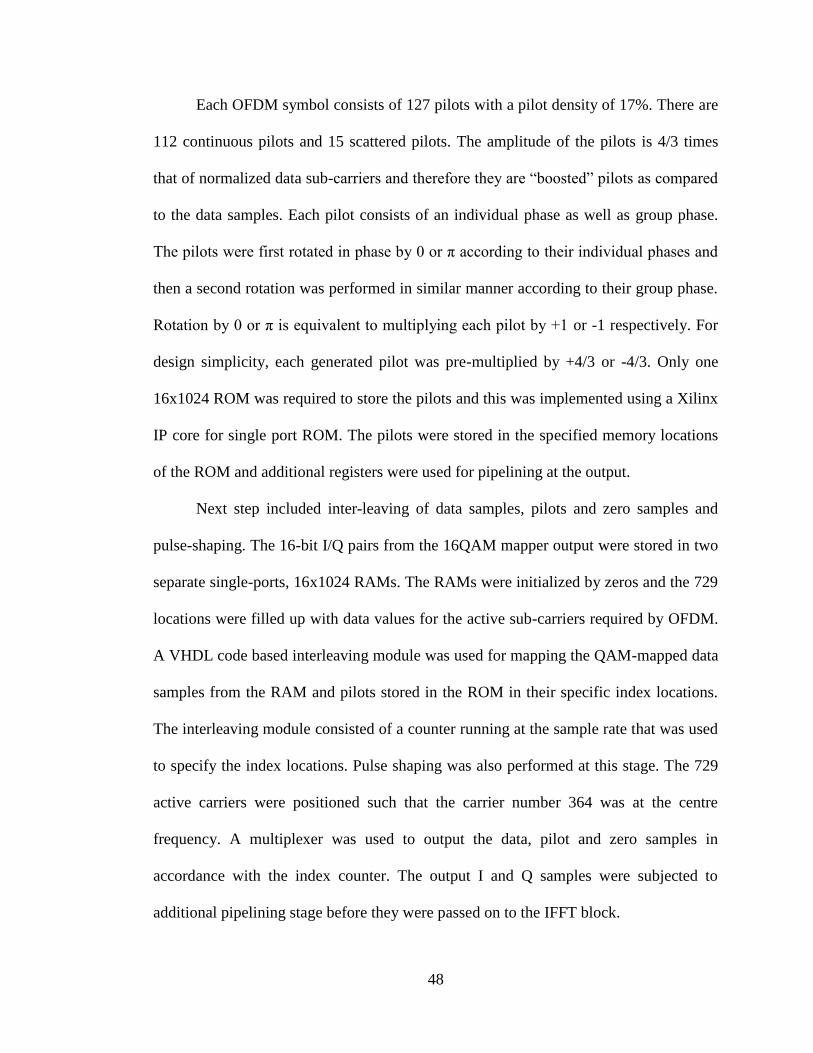
48
Each OFDM symbol consists of 127 pilots with a pilot density of 17%. There are
112 continuous pilots and 15 scattered pilots. The amplitude of the pilots is 4/3 times
that of normalized data sub-carriers and therefore they are “boosted” pilots as compared
to the data samples. Each pilot consists of an individual phase as well as group phase.
The pilots were first rotated in phase by 0 or π according to their individual phases and
then a second rotation was performed in similar manner according to their group phase.
Rotation by 0 or π is equivalent to multiplying each pilot by +1 or -1 respectively. For
design simplicity, each generated pilot was pre-multiplied by +4/3 or -4/3. Only one
16x1024 ROM was required to store the pilots and this was implemented using a Xilinx
IP core for single port ROM. The pilots were stored in the specified memory locations
of the ROM and additional registers were used for pipelining at the output.
Next step included inter-leaving of data samples, pilots and zero samples and
pulse-shaping. The 16-bit I/Q pairs from the 16QAM mapper output were stored in two
separate single-ports, 16x1024 RAMs. The RAMs were initialized by zeros and the 729
locations were filled up with data values for the active sub-carriers required by OFDM.
A VHDL code based interleaving module was used for mapping the QAM-mapped data
samples from the RAM and pilots stored in the ROM in their specific index locations.
The interleaving module consisted of a counter running at the sample rate that was used
to specify the index locations. Pulse shaping was also performed at this stage. The 729
active carriers were positioned such that the carrier number 364 was at the centre
frequency. A multiplexer was used to output the data, pilot and zero samples in
accordance with the index counter. The output I and Q samples were subjected to
additional pipelining stage before they were passed on to the IFFT block.

49
The final step was the conversion of frequency-domain data samples to time-
domain output of an OFDM transmitter. In practice, the OFDM modulators are realized
using an Inverse Fast Fourier Transform (IFFT) module. The IFFT block used is a
Xilinx FFT/IFFT IP core [41]. The 1024 I/Q pairs were applied to the input of the IFFT
block at a time. The algorithm used for the IFFT block performs continuous processing
of the input stream instead of working on a whole symbol at once. After a number of
latency cycles required by the IFFT block, a continuous streaming of output samples are
generated and Cyclic Prefix of 256 samples were added. The output of the IFFT block
was obtained in the form of OFDM symbols with a guard interval ratio of ¼. All the
components blocks used 16 bit fixed point representation with binary point at 14. The
output sample rate was 2.1511MSPS (= 8.604MBPS). A Welch power spectral density
was estimated for an OFDM symbol in MATLAB environment and shown in Fig. 4.4.
4.2 Design of a Linearizer System
The linearizer system designed in this research is based on a reference design
from Xilinx using digital predistortion method of linearization. This design is suitable
for data rate up to 92.1600MSPS with a signal bandwidth of 20MHz. The ETSI-SDR
OFDM transmitter designed in this research uses a signal bandwidth of 1.5314MHz
with a data rate of 2.1511MSPS and therefore the Xilinx reference design was found
suitable for this research. The characteristics, components and design of the linearizer
system are described in following sections.
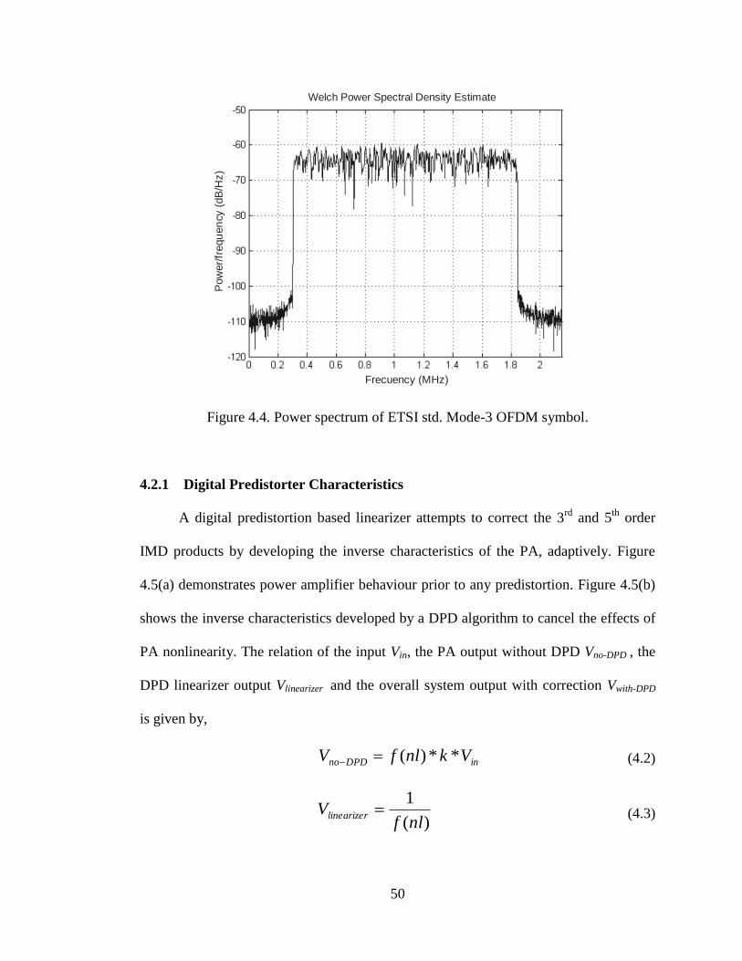
50
Figure 4.4. Power spectrum of ETSI std. Mode-3 OFDM symbol.
4.2.1 Digital Predistorter Characteristics
A digital predistortion based linearizer attempts to correct the 3rd
and 5th
order
IMD products by developing the inverse characteristics of the PA, adaptively. Figure
4.5(a) demonstrates power amplifier behaviour prior to any predistortion. Figure 4.5(b)
shows the inverse characteristics developed by a DPD algorithm to cancel the effects of
PA nonlinearity. The relation of the input Vin, the PA output without DPD Vno-DPD , the
DPD linearizer output Vlinearizer and the overall system output with correction Vwith-DPD
is given by,
inDPDno VknlfV **)( (4.2)
)(
1
nlfVlinearizer (4.3)
Welch Power Spectral Density Estimate
Pow
er/
frequ
en
cy (
dB
/Hz)
Frecuency (MHz)
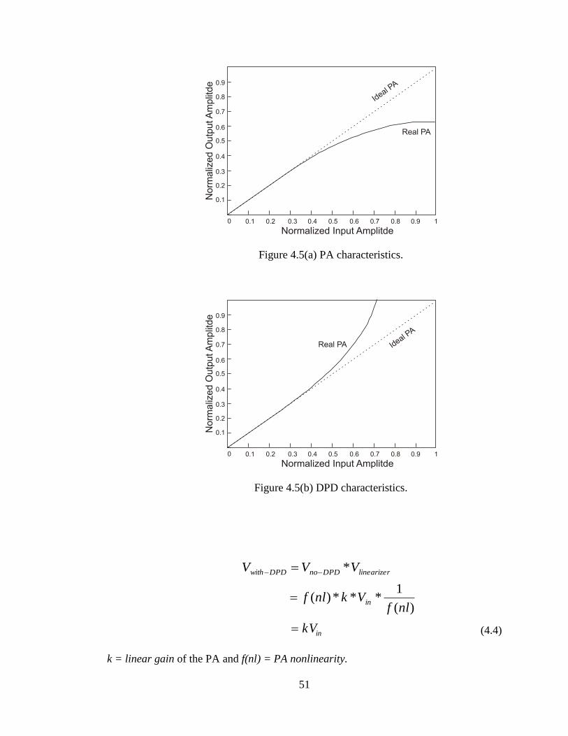
51
Figure 4.5(a) PA characteristics.
Figure 4.5(b) DPD characteristics.
linearizerDPDnoDPDwith VVV *
)(
1***)(
nlfVknlf in
inkV (4.4)
k = linear gain of the PA and f(nl) = PA nonlinearity.
52
Therefore, the output of the overall system is theoretically, linear. In practice,
however, absolute linearity is not possible. The DPD linearizer can provide an extended
linear region to the PA before saturation point allowing the input power back-off to be
reduced.
4.2.2 Digital Predistorter Functionality
A brief overview of the DPD algorithm is given here. Figure 4.6 demonstrates
the function of the algorithm. The transmitted digital data x(n) is applied to the
predistorter. The predistorter models the inverse characteristics of the PA as a function
of the magnitude of x(n). This model is a memory-polynomial model based on the
Volterra series with only the diagonal terms retained. The output of the predistorter z(n)
is amplified by the PA and the output is s(n). This output is aligned for amplitude, phase
and delay and used by the estimator. The estimator uses the output of predistorter z(n)
and the aligned output y(n) to develop the inverse coefficients of PA given by acoeff ,
such that the output s(n) is as close as possible to x(n).
4.2.3 Digital Predistortion Based Linearizer System
The reference design documents [32-34] include the design process in details
and provides for design modifications to suit the user application. The design is to be
used with a complete VHDL-based approach. It is a hardware-software co-design to
save resources on the FPGA and to make the design run faster. The software portion of
the design runs on Xilinx Microblaze embedded processor on the Xilinx Virtex-4 or
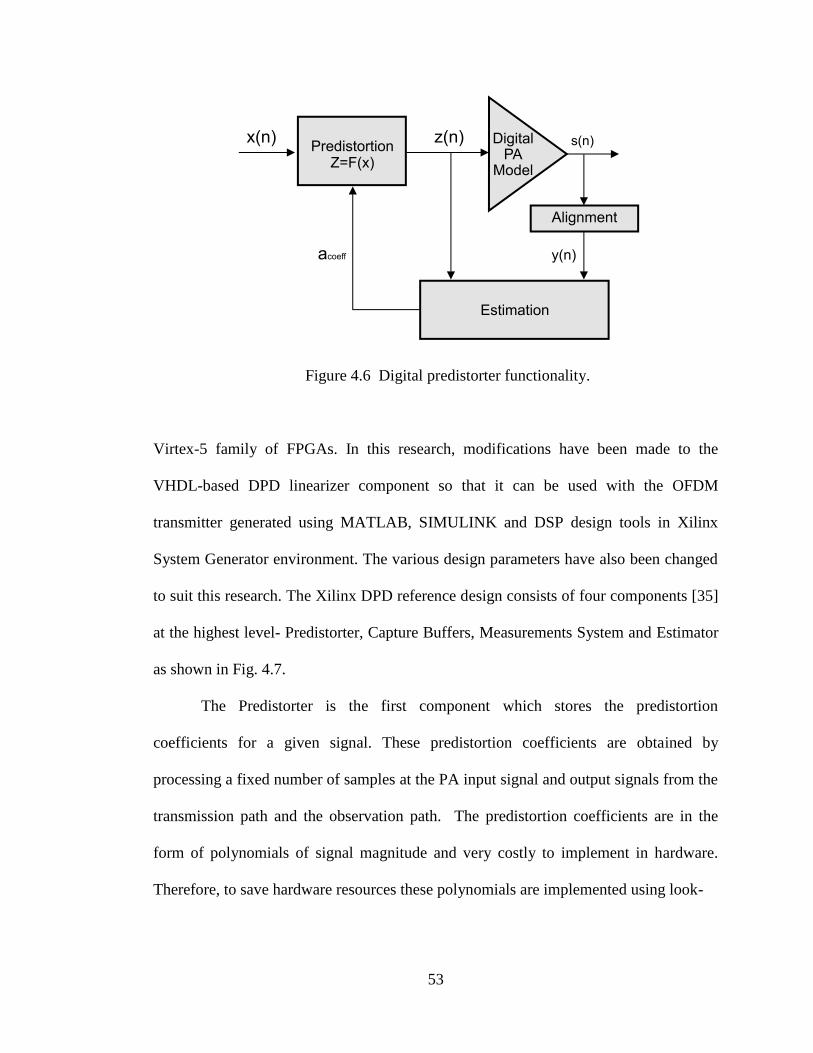
53
Figure 4.6 Digital predistorter functionality.
Virtex-5 family of FPGAs. In this research, modifications have been made to the
VHDL-based DPD linearizer component so that it can be used with the OFDM
transmitter generated using MATLAB, SIMULINK and DSP design tools in Xilinx
System Generator environment. The various design parameters have also been changed
to suit this research. The Xilinx DPD reference design consists of four components [35]
at the highest level- Predistorter, Capture Buffers, Measurements System and Estimator
as shown in Fig. 4.7.
The Predistorter is the first component which stores the predistortion
coefficients for a given signal. These predistortion coefficients are obtained by
processing a fixed number of samples at the PA input signal and output signals from the
transmission path and the observation path. The predistortion coefficients are in the
form of polynomials of signal magnitude and very costly to implement in hardware.
Therefore, to save hardware resources these polynomials are implemented using look-
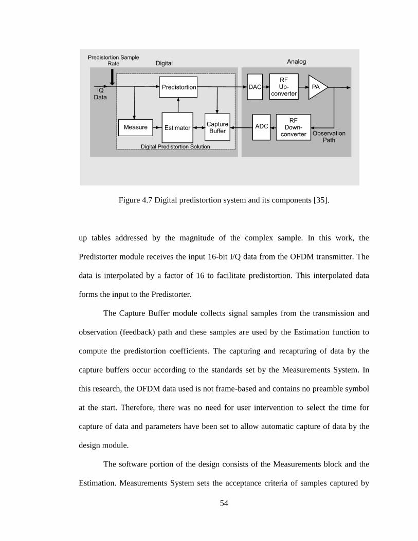
54
Figure 4.7 Digital predistortion system and its components [35].
up tables addressed by the magnitude of the complex sample. In this work, the
Predistorter module receives the input 16-bit I/Q data from the OFDM transmitter. The
data is interpolated by a factor of 16 to facilitate predistortion. This interpolated data
forms the input to the Predistorter.
The Capture Buffer module collects signal samples from the transmission and
observation (feedback) path and these samples are used by the Estimation function to
compute the predistortion coefficients. The capturing and recapturing of data by the
capture buffers occur according to the standards set by the Measurements System. In
this research, the OFDM data used is not frame-based and contains no preamble symbol
at the start. Therefore, there was no need for user intervention to select the time for
capture of data and parameters have been set to allow automatic capture of data by the
design module.
The software portion of the design consists of the Measurements block and the
Estimation. Measurements System sets the acceptance criteria of samples captured by
55
the Capture Buffers by observing the transmitted data over a defined interval. Samples
are captured, discarded and recaptured until the data captured is a good representative of
the entire signal. This makes it possible for the estimation function to successfully
compute the predistortion coefficients for the signal for a given power amplifier.
The Estimator block computes the predistortion coefficients comparing the
samples from transmitted and received data path. The Xilinx Microblaze processor
computes the predistortion coefficients and updates the look-up tables in the
Predistorter. These values are used to precondition the signal before it is transmitted by
the power amplifier such that the nonlinear characteristics of the power amplifier are
compensated for, adaptively.
The design clocks have been modified in this research to match the data rate of
various components of the OFDM transmitter. The design parameters have also been
changed so that the linearizer system accepts down-converted baseband I/Q data from
the observation path instead of an IF down-converted signal.
4.2.4 Integration of OFDM Transmitter and Linearizer System
The time-domain data generated by the OFDM transmitter when transmitted by
the RF power amplifier undergoes amplitude and phase distortion resulting in in-band
distortion and out-of-band spectral leakage. A digital predistortion based PA linearizer
system based on the reference design from Xilinx was described in the previous section.
The data generated by the OFDM modulator needed to be upsampled to a predistortion
rate which is at least 5-6 times the data rate to make digital predistortion possible. A
56
system integration of the OFDM transmitter and DPD linearizer system was also
required. The design of this system integration has been described in this section.
In this project, the data has been upsampled by a factor of 16 to comply with
D/A and A/D converters available on the Xilinx XtremeDSP Virtex-4 Development
board. The upsampling was performed in four stages using upsampler by factor of 2 for
each stage instead of using a single upsampler by factor 16. Each upsampling stage
requires a reconstruction filter, therefore, a dedicated interpolating filter performing an
upsampling by factor of 2 and image-filtering and reconstruction was used. This type of
multistage interpolating is very useful because they are easy to design and their
implementation saves resources as compared to a single interpolating filter with a very
narrow pass-band [42]. The specifications of the interpolating filter stages are given in
Table 4.2. The signal bandwidth is 1.5314MHz. The pass band frequency fc in MHz for
each filter stage m is given by,
12
_
mc
bandwidthsignalf (4.5)
The sampling frequency in MHz is given by Fs and the normalized pass band frequency
in radian/sample is given by,
s
cc
F
fw
2
k
fc (4.6)
where, Fs = 2.1511MHz and the normalizing factor k= Fs/2.
The interpolating filters were designed using MATLAB Filter Design (FDA)
tools. Half-band FIR filters were used to implement the filters. Every alternate
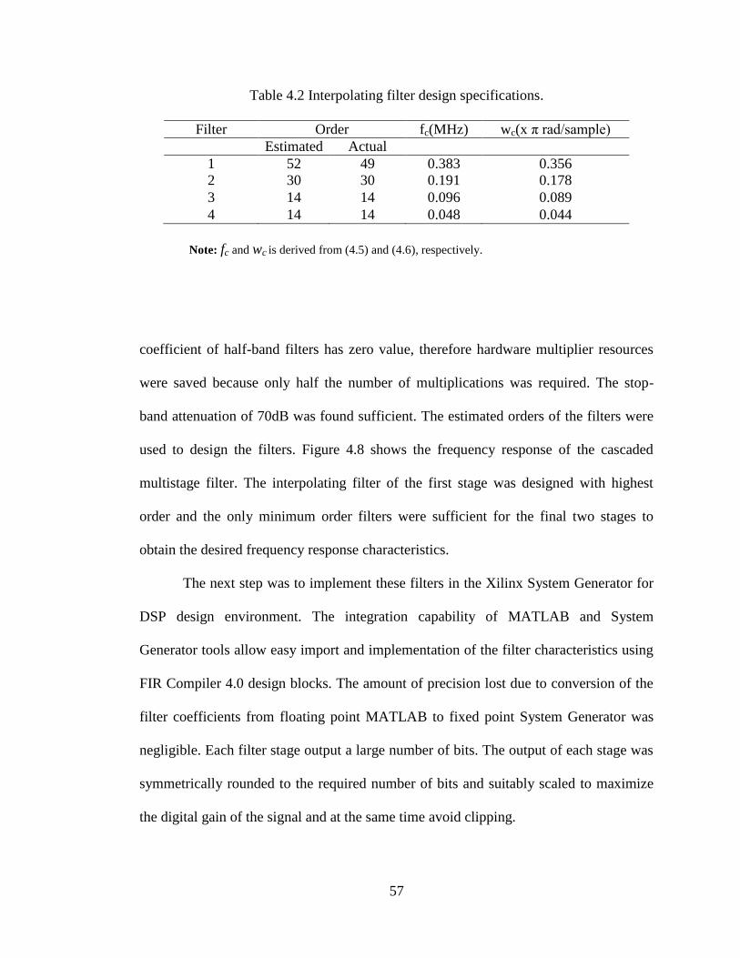
57
Table 4.2 Interpolating filter design specifications.
Filter
Stage(m)
Order fc(MHz) wc(x π rad/sample) Estimated Actual
1 52 49 0.383 0.356
2 30 30 0.191 0.178
3 14 14 0.096 0.089
4 14 14 0.048 0.044
Note: fc and wc is derived from (4.5) and (4.6), respectively.
coefficient of half-band filters has zero value, therefore hardware multiplier resources
were saved because only half the number of multiplications was required. The stop-
band attenuation of 70dB was found sufficient. The estimated orders of the filters were
used to design the filters. Figure 4.8 shows the frequency response of the cascaded
multistage filter. The interpolating filter of the first stage was designed with highest
order and the only minimum order filters were sufficient for the final two stages to
obtain the desired frequency response characteristics.
The next step was to implement these filters in the Xilinx System Generator for
DSP design environment. The integration capability of MATLAB and System
Generator tools allow easy import and implementation of the filter characteristics using
FIR Compiler 4.0 design blocks. The amount of precision lost due to conversion of the
filter coefficients from floating point MATLAB to fixed point System Generator was
negligible. Each filter stage output a large number of bits. The output of each stage was
symmetrically rounded to the required number of bits and suitably scaled to maximize
the digital gain of the signal and at the same time avoid clipping.
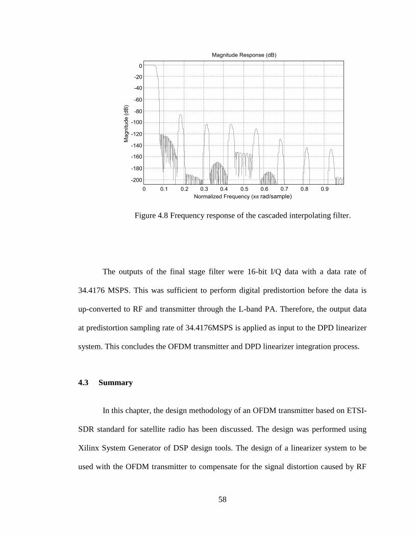
58
Figure 4.8 Frequency response of the cascaded interpolating filter.
The outputs of the final stage filter were 16-bit I/Q data with a data rate of
34.4176 MSPS. This was sufficient to perform digital predistortion before the data is
up-converted to RF and transmitter through the L-band PA. Therefore, the output data
at predistortion sampling rate of 34.4176MSPS is applied as input to the DPD linearizer
system. This concludes the OFDM transmitter and DPD linearizer integration process.
4.3 Summary
In this chapter, the design methodology of an OFDM transmitter based on ETSI-
SDR standard for satellite radio has been discussed. The design was performed using
Xilinx System Generator of DSP design tools. The design of a linearizer system to be
used with the OFDM transmitter to compensate for the signal distortion caused by RF

59
power amplifiers was also described. The linearizer system is based up on a DPD
linearizer reference design from Xilinx. The system integration process including the
predistortion rate upsampling of OFDM data was presented. Next chapter presents the
simulation of the OFDM transmitter-linearizer system.
60
5. SIMULATION
Before the OFDM transmitter and linearizer system described in the previous
chapter can be implemented in FPGA platform, the design needed to be verified in a
simulation environment. The simulation was performed in an integrated environment of
MATLAB, SIMULINK and Xilinx System Generator for DSP. A simulation model of
an RF power amplifier operating at an L-band frequency was developed. The PA
simulation model was used in the transmitter path to verify the functionality of the
OFDM transmitter with and without DPD linearizer correction. The following sections
describe the modeling and the simulation process.
5.1 Modeling of Power Amplifier
5.1.1 AM-AM and AM-PM Characterization
The RF Power Amplifier used in this research is currently used at SED Systems,
Saskatoon. It is a travelling wave tube amplifier (TWTA) suitable for SDR transmission
systems, operating in the L-band frequency range of 1.450 – 1.490GHz. The operating
frequency was chosen at 1.475GHz and the relationship between input power
magnitude and output power magnitude and phase-shift were obtained experimentally.
The linear gain and phase-shift of the high power amplifier has been suitably scaled to
facilitate modeling in simulation environment as given in Table 5.1.
61
The experimental data was used to obtain the AM-AM and AM-PM
characteristics of the PA as described in Section 2.2 of Chapter 2. First the input power
magnitude and output power magnitude in dB were used to calculate the linear
relationship between input sample magnitude and output sample magnitude as given by
the following equation,
)20
(
10dBmP
nz (5.1)
PdBm is the power magnitude in dBm of the nth
complex sample z n with magnitude | z n |
in mV.
5.1.2 Polynomial Curve-fitting
The AM-AM and AM-PM equations were formed using MATLAB version
R2007a. The data sets of input sample magnitude and output sample magnitude, as
derived from Table 5.1, were used to obtain coefficients for AM-AM equations.
Similarly, the input sample magnitude and phase-shift relationship derived from Table
5.1 was used to obtain coefficients for AM-PM equations. The data sets were plotted on
a two-dimensional plane and MATLAB curve-fitting toolbox was used to find the best
fit from the plotted data points.
The goodness of fit was determined using three main fit statistics criteria. These
are squared sum of error (SSE), adjusted R-square and root mean square error (RMSE)
as given in MATLAB R2007a documentation [37] for curve-fitting toolbox. The SSE
gives the total deviation of the data sets from the fit and should be as close to „0‟ as
possible. Adjusted R-square is a correlation statistic between predicted and actual data
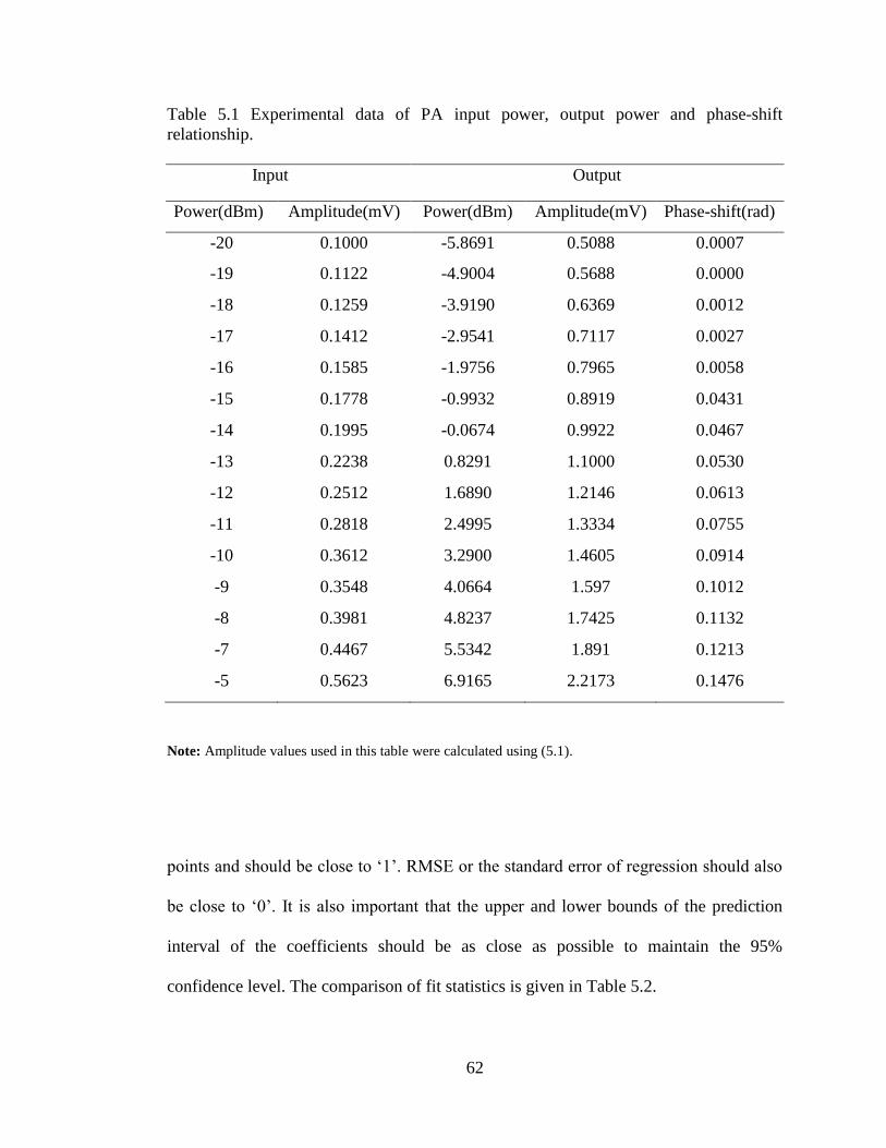
62
Table 5.1 Experimental data of PA input power, output power and phase-shift
relationship.
Input Output
Power(dBm) Amplitude(mV) Power(dBm) Amplitude(mV) Phase-shift(rad)
-20 0.1000 -5.8691 0.5088 0.0007
-19 0.1122 -4.9004 0.5688 0.0000
-18 0.1259 -3.9190 0.6369 0.0012
-17 0.1412 -2.9541 0.7117 0.0027
-16 0.1585 -1.9756 0.7965 0.0058
0.0431
0.0467
0.0530
0.0613
0.0755
0.0914
0.1012
0.1132
0.1213
0.1476
-15 0.1778 -0.9932 0.8919 0.0431
0.0467
0.0530
0.0613
0.0755
0.0914
0.1012
0.1132
-14 0.1995 -0.0674 0.9922 0.0467
0.0530
0.0613
0.0755
0.0914
0.1012
0.1132
0.1213
0.1476
-13 0.2238 0.8291 1.1000 0.0530
-12 0.2512 1.6890 1.2146 0.0613
-11 0.2818 2.4995 1.3334 0.0755
-10 0.3612 3.2900 1.4605 0.0914
-9 0.3548 4.0664 1.597 0.1012
-8 0.3981 4.8237 1.7425 0.1132
-7 0.4467 5.5342 1.891 0.1213
-5 0.5623 6.9165 2.2173 0.1476
Note: Amplitude values used in this table were calculated using (5.1).
points and should be close to „1‟. RMSE or the standard error of regression should also
be close to „0‟. It is also important that the upper and lower bounds of the prediction
interval of the coefficients should be as close as possible to maintain the 95%
confidence level. The comparison of fit statistics is given in Table 5.2.
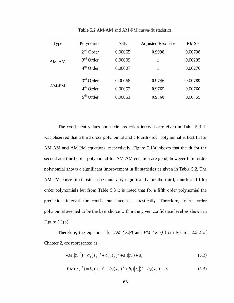
63
Table 5.2 AM-AM and AM-PM curve-fit statistics.
Type Polynomial SSE Adjusted R-square RMSE
AM-AM
2nd
Order 0.00065 0.9998 0.00738
3rd
Order 0.00009 1 0.00295
4th
Order 0.00007 1 0.00276
AM-PM
3rd
Order 0.00068 0.9746 0.00789
4th
Order 0.00057 0.9765 0.00760
5th
Order 0.00051 0.9768 0.00755
The coefficient values and their prediction intervals are given in Table 5.3. It
was observed that a third order polynomial and a fourth order polynomial is best fit for
AM-AM and AM-PM equations, respectively. Figure 5.1(a) shows that the fit for the
second and third order polynomial for AM-AM equation are good, however third order
polynomial shows a significant improvement in fit statistics as given in Table 5.2. The
AM-PM curve-fit statistics does not vary significantly for the third, fourth and fifth
order polynomials but from Table 5.3 it is noted that for a fifth order polynomial the
prediction interval for coefficients increases drastically. Therefore, fourth order
polynomial seemed to be the best choice within the given confidence level as shown in
Figure 5.1(b).
Therefore, the equations for AM (|zn|²) and PM (|zn|²) from Section 2.2.2 of
Chapter 2, are represented as,
01
2
2
3
3
2)()()()( azazazazAM nnnn
(5.2)
01
2
2
3
3
4
4
2)()()()()( bzbzbzbzbzPM nnnnn (5.3)

64
Table 5.3 AM-AM and AM-PM curve-fit coefficients.
Order AM-AM Equation Order
Order
AM-PM Equation
Coefficient Prediction Coefficient Prediction Interval Interval
2
3
b3 -0.001 (-2.877, 2.875)
a2 -2.954 (-3.185, -2.724) b2 -0.450 (-3.284, 2.383)
a1 5.624 (5.478, 5.770) b1 0.634 (-0.198, 1.466)
a0 -0.020 (-0.040,-0.001) b0 -0.067 (-0.138, 0.003)
3
4
b4 11.930 (-15.860, 39.720)
a3 2.774 (2.013, 3.535) b3 -15.420 (-51.440, 20.600)
a2 -5.666 (-6.415, -4.916) b2 6.369 (-9.754, 22.490)
a1 6.397 (6.177, 6.617) b1 -0.569 (-3.488, 2.349)
a0 -0.082 (-0.101, -0.063) b0 0.003 (-0.175, 0.181)
4
5
b5 -99.760 (-403.900, 204.400)
a4 5.049 (-2.051, 12.150) b4 169.600 (-311.900, 651.000)
a3 -3.750 (-12.950, 5.453) b3 -108.500 (-394.800, 177.700)
a2 -2.780 (-6.900, 1.339) b2 31.840 (-47.530, 111.200)
a1 5.888 (5.142, 6.634) b1 -3.766 (-13.960, 6.424)
a0 -0.052 (-0.098, -0.007) b0 0.149 (-0.332, 0.631)
where, a0, a1, a2, a3 and b0, b1, b2, b3, b4 are the coefficient sets for AM (|zn|²) and PM
(|zn|²), respectively.
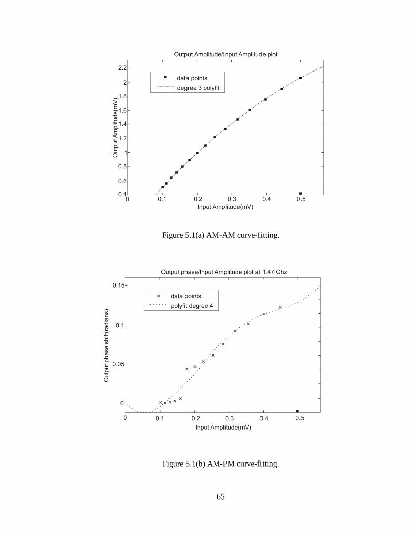
65
Figure 5.1(a) AM-AM curve-fitting.
Figure 5.1(b) AM-PM curve-fitting.
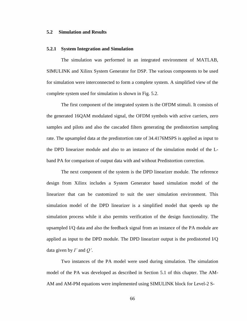
66
5.2 Simulation and Results
5.2.1 System Integration and Simulation
The simulation was performed in an integrated environment of MATLAB,
SIMULINK and Xilinx System Generator for DSP. The various components to be used
for simulation were interconnected to form a complete system. A simplified view of the
complete system used for simulation is shown in Fig. 5.2.
The first component of the integrated system is the OFDM stimuli. It consists of
the generated 16QAM modulated signal, the OFDM symbols with active carriers, zero
samples and pilots and also the cascaded filters generating the predistortion sampling
rate. The upsampled data at the predistortion rate of 34.4176MSPS is applied as input to
the DPD linearizer module and also to an instance of the simulation model of the L-
band PA for comparison of output data with and without Predistortion correction.
The next component of the system is the DPD linearizer module. The reference
design from Xilinx includes a System Generator based simulation model of the
linearizer that can be customized to suit the user simulation environment. This
simulation model of the DPD linearizer is a simplified model that speeds up the
simulation process while it also permits verification of the design functionality. The
upsampled I/Q data and also the feedback signal from an instance of the PA module are
applied as input to the DPD module. The DPD linearizer output is the predistorted I/Q
data given by I’ and Q’.
Two instances of the PA model were used during simulation. The simulation
model of the PA was developed as described in Section 5.1 of this chapter. The AM-
AM and AM-PM equations were implemented using SIMULINK block for Level-2 S-
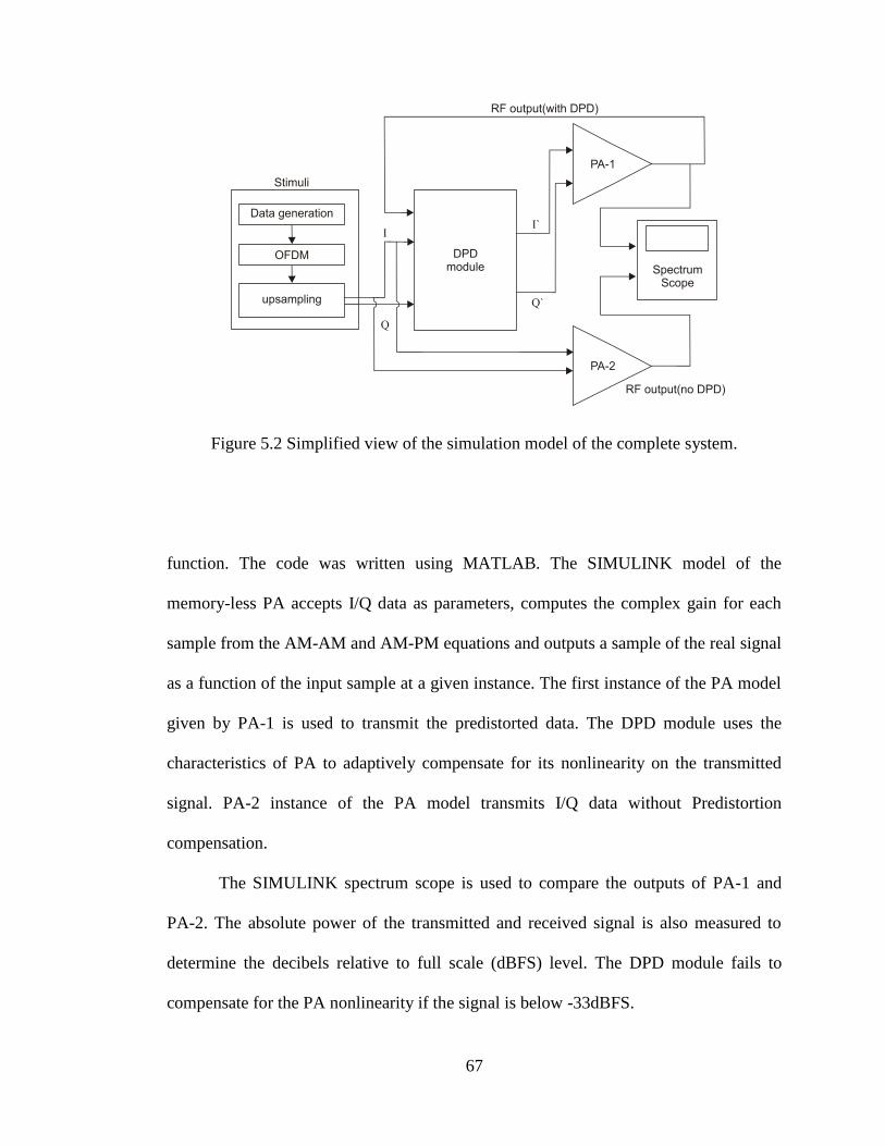
67
Figure 5.2 Simplified view of the simulation model of the complete system.
function. The code was written using MATLAB. The SIMULINK model of the
memory-less PA accepts I/Q data as parameters, computes the complex gain for each
sample from the AM-AM and AM-PM equations and outputs a sample of the real signal
as a function of the input sample at a given instance. The first instance of the PA model
given by PA-1 is used to transmit the predistorted data. The DPD module uses the
characteristics of PA to adaptively compensate for its nonlinearity on the transmitted
signal. PA-2 instance of the PA model transmits I/Q data without Predistortion
compensation.
The SIMULINK spectrum scope is used to compare the outputs of PA-1 and
PA-2. The absolute power of the transmitted and received signal is also measured to
determine the decibels relative to full scale (dBFS) level. The DPD module fails to
compensate for the PA nonlinearity if the signal is below -33dBFS.
68
5.2.2 Results
The simulation results showed that the OFDM transmitter generated a data at the
rate of 2.1511MSPS with a signal bandwidth of 1.5314MHz. The cascaded filter stages
upsampled the data by a factor 16 to obtain a sample rate of 34.4176MSPS. The results
of comparison of output signals with and without DPD are shown in Fig. 5.3, which is a
display of the SIMULINK Spectrum Scope for a span of ± sampling frequency/2
(sampling frequency = 34.4176MHz).
The spacing between the channels is 1.712MHz for the given standard.
Measurement was taken at a distance of 1.5MHz from the carrier center frequency and
reduction in spectral regrowth close to 11dB was observed. It is to be mentioned that
this simulation did not involve up-conversion and down-conversion to and from RF and
it only attempts to observe and verify the behavior and functionality of the system,
under ideal conditions.
5.3 Summary
In this chapter, the simulation method of the OFDM transmitter and linearizer
system was described and results of simulation were presented.
A simulation model of the L-band PA was developed using
MATLAB/SIMULINK using the AM-AM and AM-PM characteristic equations at an
L-band frequency of 1.475GHz. Polynomials of degree 3 and a polynomial of degree 4
were sufficient for modeling the AM-AM and AM-PM characteristics of the RF power
amplifier. The OFDM transmission system, the cascaded filters performing upsampling
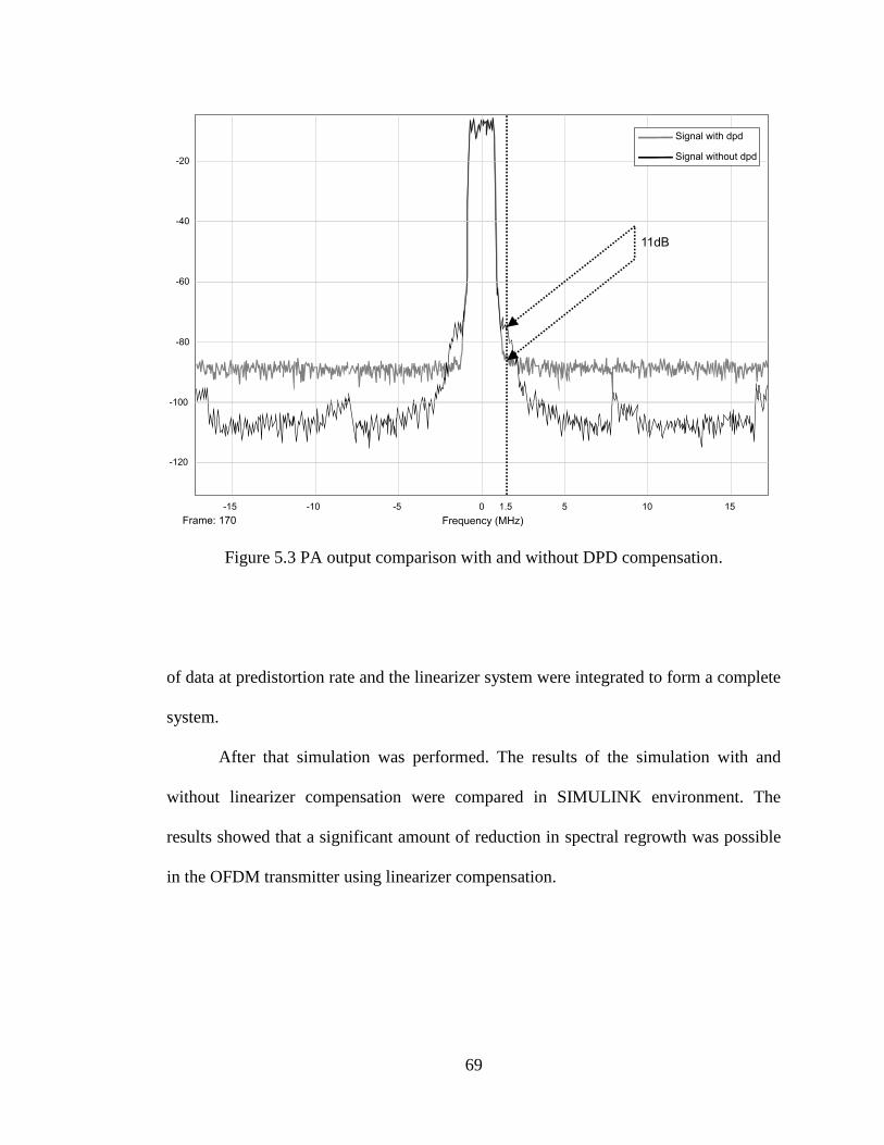
69
Figure 5.3 PA output comparison with and without DPD compensation.
of data at predistortion rate and the linearizer system were integrated to form a complete
system.
After that simulation was performed. The results of the simulation with and
without linearizer compensation were compared in SIMULINK environment. The
results showed that a significant amount of reduction in spectral regrowth was possible
in the OFDM transmitter using linearizer compensation.
70
6. IMPLEMENTATION, RESULTS AND ANALYSIS
The ETSI-SDR OFDM transmitter and the DPD based linearizer system
performed as expected during simulation. As a next step, the transmitter and the
linearizer system was implemented on the FPGA platform. A hardware test setup was
also built for performance testing at RF. The RF power amplifier operating at an L-band
frequency of 1.475GHz was used in the transmitter path. The testing hardware was built
using commercially available components and evaluation boards. No custom hardware
was built.
The results of the hardware testing were compared with the simulation results.
The details of hardware implementation, results and analysis are presented in this
chapter.
6.1 Hardware Implementation
The complete schematic of the hardware implementation with the signal flow
path is shown in Fig. 6.1 and the described in details in the following subsections.
6.1.1 FPGA Implementation of OFDM Transmitter and DPD Linearizer
The FPGA implementation of the design of the ETSI-SDR OFDM transmitter
and the digital predistortion based linearizer consisted of two parts. The design clocks
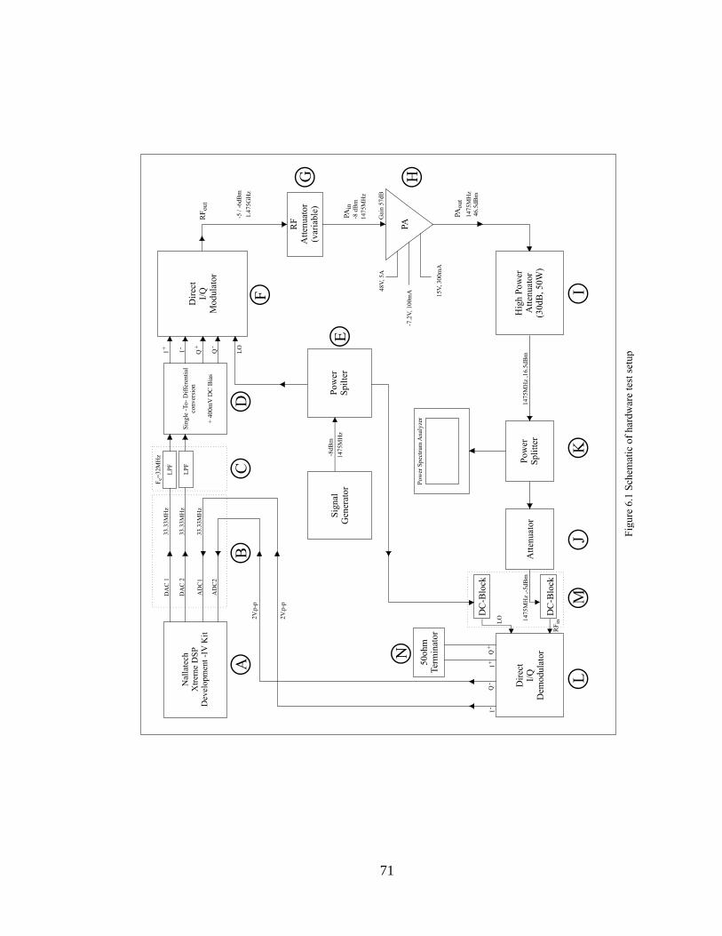
71
72
were generated using the Virtex-4 FPGA XC4VSX35 of speed grade -10 and Virtex-II
clock FPGA XC2V80 of speed grade -4 found on the Nallatech XtremeDSP
Development Kit-IV evaluation board [43]. The design logic was implemented on
Virtex-4 FPGA. The picture of the Nallatech XtremeDSP Development Kit-IV
evaluation board is shown in Appendix B. The design synthesis, implementation and
generation of bit files suitable for loading onto the FPGAs was performed in Project
Navigator environment of Xilinx ISE Foundation 10.1.3 software. The generated bit
files were loaded on to the FPGAs using the Nallatech FUSE software. The on-board
clocks and resets were also set through the FUSE software. The clock structure
generated by the two FPGAs for the design is given in Fig. 6.2.
The main design clock was generated at 33.33MHz using the onboard
programmable oscillator on Virtex-4 XC4VSX35 FPGA. This clock was used as an
input to the clock FPGA Virtex-II XC2V80 and various clock interfaces were designed.
This clock was used to generate the clocks for the on-board A/D and D/A converters at
33.33MHz. A feedback clock signal was brought back to the Virtex-4 FPGA and used
as an input to the digital clock manager (DCM) [44]. The feedback signal synchronized
the clocks to the D/A and A/D converters and the rest of the design logic.
The DCM was used to derive various clocks used in the OFDM transmitter and
the DPD linearizer system. The input clock of 33.33MHz was used to derive an output
clock at the same rate (clk_0). This output clock buffered using a global clock buffer
(BUFG) and provided feed back to the DCM and the reset signal for the DCM was
provided by the FPGA reset. The “locked” output of DCM is high only after the output
clocks are stable and can be used to ensure stability of output clocks. The output clock
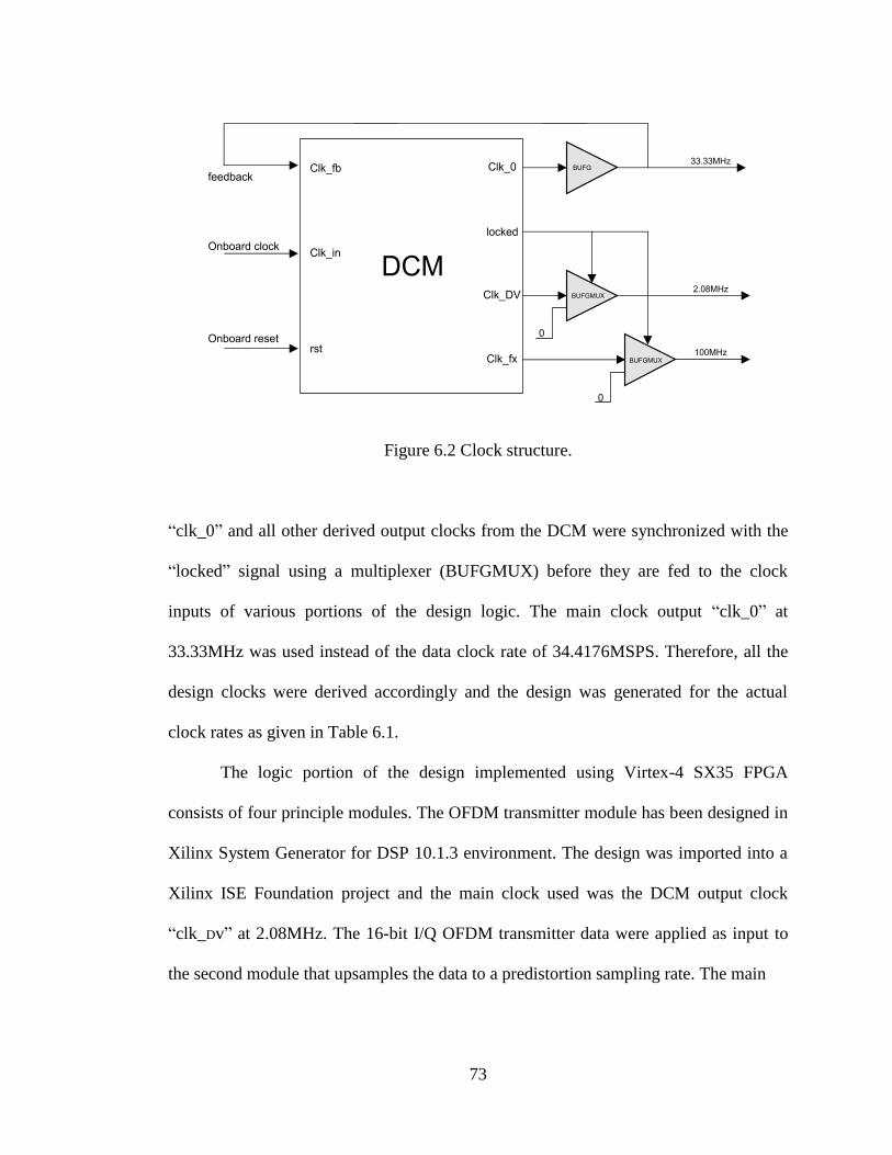
73
Figure 6.2 Clock structure.
“clk_0” and all other derived output clocks from the DCM were synchronized with the
“locked” signal using a multiplexer (BUFGMUX) before they are fed to the clock
inputs of various portions of the design logic. The main clock output “clk_0” at
33.33MHz was used instead of the data clock rate of 34.4176MSPS. Therefore, all the
design clocks were derived accordingly and the design was generated for the actual
clock rates as given in Table 6.1.
The logic portion of the design implemented using Virtex-4 SX35 FPGA
consists of four principle modules. The OFDM transmitter module has been designed in
Xilinx System Generator for DSP 10.1.3 environment. The design was imported into a
Xilinx ISE Foundation project and the main clock used was the DCM output clock
“clk_Dv” at 2.08MHz. The 16-bit I/Q OFDM transmitter data were applied as input to
the second module that upsamples the data to a predistortion sampling rate. The main
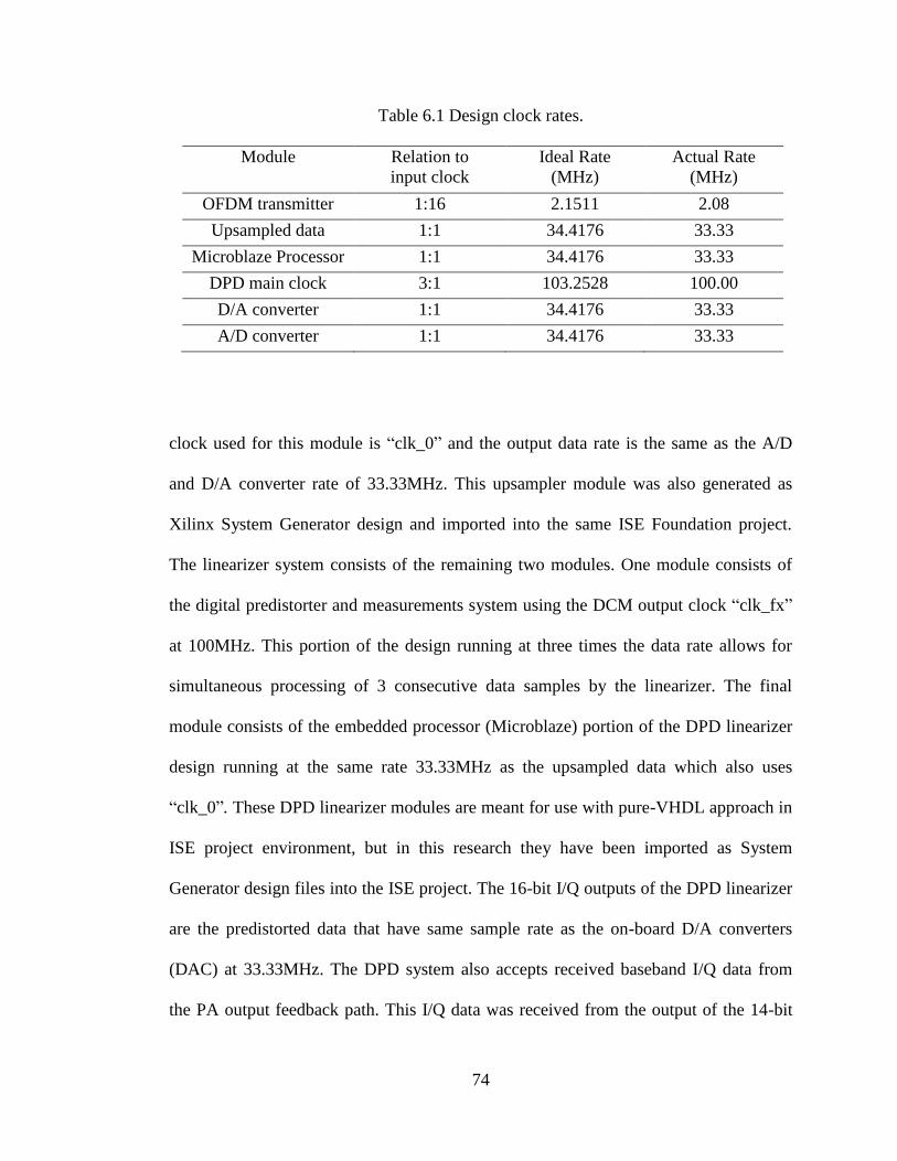
74
Table 6.1 Design clock rates.
Module Relation to
input clock
Ideal Rate
(MHz)
Actual Rate
(MHz)
OFDM transmitter 1:16 2.1511 2.08
Upsampled data 1:1 34.4176 33.33
Microblaze Processor 1:1 34.4176 33.33
DPD main clock 3:1 103.2528 100.00
D/A converter 1:1 34.4176 33.33
A/D converter 1:1 34.4176 33.33
clock used for this module is “clk_0” and the output data rate is the same as the A/D
and D/A converter rate of 33.33MHz. This upsampler module was also generated as
Xilinx System Generator design and imported into the same ISE Foundation project.
The linearizer system consists of the remaining two modules. One module consists of
the digital predistorter and measurements system using the DCM output clock “clk_fx”
at 100MHz. This portion of the design running at three times the data rate allows for
simultaneous processing of 3 consecutive data samples by the linearizer. The final
module consists of the embedded processor (Microblaze) portion of the DPD linearizer
design running at the same rate 33.33MHz as the upsampled data which also uses
“clk_0”. These DPD linearizer modules are meant for use with pure-VHDL approach in
ISE project environment, but in this research they have been imported as System
Generator design files into the ISE project. The 16-bit I/Q outputs of the DPD linearizer
are the predistorted data that have same sample rate as the on-board D/A converters
(DAC) at 33.33MHz. The DPD system also accepts received baseband I/Q data from
the PA output feedback path. This I/Q data was received from the output of the 14-bit

75
A/D convertors (ADC) at 33.33MHz. The 16-bit I/Q transmitted data from the DPD
linearizer is rounded to 14 bits to match the maximum number of bits allowed by the
DACs. Conversely, the 14-bit received data from the ADCs were zero-stuffed and used
by the 16-bit input ports of the DPD linearizer.
These two ISE Foundation projects for the Virtex-II and Virtex-4 FPGAs were
synthesized, implemented and then the generated bit files are loaded on to the respective
FPGAs using FUSE software [43]. The digitally predistorted I/Q data output from the
Virtex-4 FPGA were applied as input to the two separate D/A converters for
transmission.
6.1.2 Transmission Path
The transmission path of the test hardware setup is shown in Fig. 6.3 and can be
compared with the points A-F in Fig. 6.1. The various components have been identified
in the Figures and described in this section.
FPGA board and DAC: The first part of the transmission path hardware is the
Nallatech XtremeDSP Development Kit-IV evaluation board (point A). The digitally
predistorted I/Q data from the output of the Virtex-4 FPGA is sampled at the rate of
33.33MHz by the two D/A converters (point B) available on the evaluation board as a
part of the XtremeDSP Development Kit-IV. The D/A converters (DAC) are 14-bit
resolution AD9772A manufactured by Analog Devices Inc. The DAC interface with the
FPGAs is shown in Appendix B. The maximum data rate is 160MSPS which is
sufficient for data rate of 33.33MSPS as used in this work. The interpolation filters on
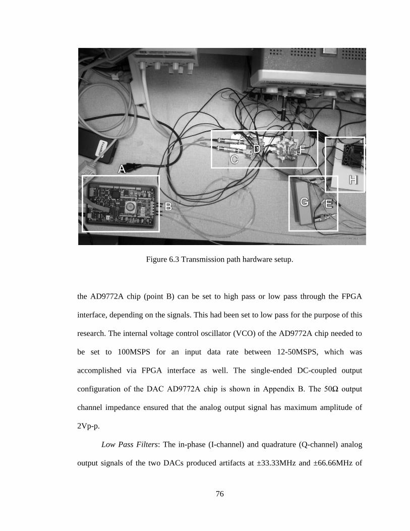
76
Figure 6.3 Transmission path hardware setup.
the AD9772A chip (point B) can be set to high pass or low pass through the FPGA
interface, depending on the signals. This had been set to low pass for the purpose of this
research. The internal voltage control oscillator (VCO) of the AD9772A chip needed to
be set to 100MSPS for an input data rate between 12-50MSPS, which was
accomplished via FPGA interface as well. The single-ended DC-coupled output
configuration of the DAC AD9772A chip is shown in Appendix B. The 50Ω output
channel impedance ensured that the analog output signal has maximum amplitude of
2Vp-p.
Low Pass Filters: The in-phase (I-channel) and quadrature (Q-channel) analog
output signals of the two DACs produced artifacts at ±33.33MHz and ±66.66MHz of
77
the main carrier frequency, which could not be removed by the 100MHz filters on the
AD9772A chips. Therefore, baseband analog filtering was required. Analog low pass
filters BLP-30 manufactured by Mini-Circuits was used (point C). These 50Ω
impedance analog filters having a pass-band of DC-32MHz [45] successfully filtered
the artifacts, when used in-line with the DAC channels.
Single-to-differential circuit, Power splitter and Quadrature Modulator: The
filtered outputs of the DAC channels were suitable for up-conversion to RF. The
quadrature modulator AD8349 evaluation board (point F) manufactured by Analog
Devices Inc. was used for direct conversion from baseband to RF at 1.475GHz. The
single-ended signals, however, needed to be converted to differential inputs for the
AD8349 evaluation board. The single-to-differential conversion and adding 400mV DC
bias to the signals as required by the AD8349 specifications [46] was performed using
AD8132 differential amplifiers manufactured by Analog Devices Inc. The interface
circuit (point D) between AD8132 and AD8349 board is given in Appendix C. The
AD8132 chips use a supply of ±5V DC and therefore a single DC power supply of 5V
was required. The baseband to RF direct up-conversion to 1.475GHz L-band frequency
was performed on the differential input signals by the AD8349.
The AD8349 evaluation board uses +5V from the supply. Therefore, the same
power supply was used as the AD8132 chips and the ground pins were connected to the
common ground. The AD8349 required a maximum differential input of 1.2Vp-p for
optimum performance without clipping, using +5V DC supply. The differential outputs
of the AD8132 were found compliant with these specifications; therefore, no adjustment
of the signal gain was required. A single local oscillator (LO) was sufficient for the
78
signal up-conversion to RF in the transmission path and down-conversion to baseband
in PA feedback path. Agilent E4437B signal generator was used to generate a sinusoid
of -8dBm at 1.475GHz which was applied to the input of a 2-way power splitter ZFSC-
2-2500 (point E) manufactured by Mini-Circuits. One output of the 2-way splitter was
applied to the LO input port of AD8349 Evaluation board. The single-ended LO input
port on the AD8349 board includes DC blocking circuitry; therefore no external DC
blocking was required. The four differential inputs I+, Q
+, I
- and Q
- on the AD8349 use
the filtered, DC-biased, single-to-differential converted signals; therefore, no baseband
filter circuit was required on the AD8349 board. The LO signal performed the mixing
and up-conversion to the LO RF frequency by direct baseband-to-RF conversion. The
single-ended output analog signal from AD8349 board was obtained at 1.475GHz. This
is the up-converted OFDM transmitter output with a total transmitted power of -5dBm
to -6dBm.
6.1.3 L-Band Power Amplifier
Variable Attenuator, L-band PA: The test amplifier used and the PA feedback
path hardware setup are shown in Figures 6.1 and 6.4.The PA (point H) used for testing
has been developed by SED Systems. The three main components used in cascade are
Mini-circuits co-axial amplifier ZFL-2500HV (10-2500MHz), RF power metal-
semiconductor field effect transistors (MESFET) manufactured by CREE, CRF24060
(up to 2400MHz) and CRF24010 (up to 2700MHz) [47, 48]. The PA operates at an L-
band frequency range of 1.450-1.490GHz. For this research, the operating frequency
chosen was 1.475GHz. The total gain of the amplifier was 57dB.

79
Figure 6.4 Power amplifier and feedback path hardware setup.
The PA uses three power supplies for its operation. A power supply of +15V,
300mA (max) was required for the ZFL-2500HV amplifier. The MESFETs required a
common drain-to-source voltage of +48V, and the current limit was set to 5A. A -7.2V
DC supply was applied to the gate of the MESFETs with a current limit of 100mA. The
ground pins of all the components were tied to a common ground. The PA
characteristics showed that the 1dB compression point (P-1dB) is -11dBm. The PA
draws around 3A current at this point. Increasing the input to -5dBm drives the PA into
saturation and the current drawn is around 5A. The DPD linearization is possible only
when the PA did not reach saturation region, linearization fails once the PA is saturated.

80
The total input power found suitable for this work was around -8dBm to -9dBm.
Therefore an RF Variable Attenuator HP8494B from Hewlett Packard was used (point
G) to attenuate the input power of the output signal of the AD8349 board to the desired
level.
6.1.4 Feedback Path
The input signal at -8dBm to -9dBm showed significant amount of spectral
regrowth after amplification by the PA at 1.475GHz frequency. The feedback path
hardware was required to bring the PA output signal back to the FPGA device Virtex-4
to perform DPD correction on the OFDM transmitter data before it was applied to the
DACs. The hardware setup is shown in Fig. 6.4 and can be compared with points I-N
and A-B in Fig. 6.1.
High Power Attenuator and Power Splitter: The output signal power from the
high gain PA is around 46.5dBm for an input signal power of -8dBm. The output signal
power level needed to be sufficiently attenuated to render it suitable for down-
conversion to baseband frequency. A high power Attenuator (30dB, 50Watt)
manufactured by Aeroflex was used for this purpose (point I). The Agilent power
spectrum analyzer (PSA) model 8564EC allows a maximum input power of +30dBm.
Therefore, no additional attenuation was required to view the spectrum of the output of
the high power attenuator having a total power of around +16.5dBm. A 2-way power
splitter ZFSC-2-2500 (2500MHz, 0.5Watt (max)) from Mini-circuits was used (point K)
to split the output of the 50Watt high power attenuator. One output of this power splitter
was used to view the spectrum of the attenuated output signal of the PA on the PSA.
81
The second output of the power splitter was required by the down-converting mixer for
RF to direct baseband down-conversion of the RF signal.
Quadrature Demodulator, Attenuator and DC Blocks: The direct conversion
quadrature demodulator evaluation board LT5575 (point L) manufactured by Linear
Technology [49] was used for down-conversion to baseband. This evaluation board is
highly linear with maximum input power rating of +20dBm and a very high P-1dB.
However, the RF signal in this feedback path needed to be further attenuated by 10dB to
reduce distortion of the output signal. A variable attenuator HP 8494A manufactured by
Hewlett Packard was used (point J) to achieve the desired attenuation level. The output
of HP 8494A attenuator was suitable to be down-converted using the LT5575
evaluation board. The LO signal same as the RF up-converting AD8349 evaluation
board was used for the LT5575 down-converting mixer. The second output of the power
splitter (point E) provided the required -8dBm LO signal at 1.475GHz to the LT5575
Evaluation board. The single-ended LO and RF input ports of the LT5575 boards
include no additional circuitry for DC blocking. Coaxial DC blocks BLK-18-S+
(point
M) manufactured by Mini-circuits were connected at the two input ports of the LT5575
board, before the LO and RF signals at 1.475GHz were applied to those ports. The
LT5575 board used the LO signal at 1.475GHz to down-convert the RF feedback signal
at 1.475GHz from the PA output to baseband I/Q signals.
50Ω Termination: The outputs of the LT5575 board were baseband down-
converted differential signals I+, Q
+, I
- and Q
-.The A/D converters (ADC) on the
XtremeDSP Development-IV evaluation board manufactured by Nallatech only accept
single-ended analog input signals. Therefore, I- and Q
- outputs of the LT5575 board
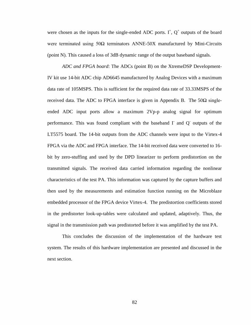
82
were chosen as the inputs for the single-ended ADC ports. I+, Q
+ outputs of the board
were terminated using 50Ω terminators ANNE-50X manufactured by Mini-Circuits
(point N). This caused a loss of 3dB dynamic range of the output baseband signals.
ADC and FPGA board: The ADCs (point B) on the XtremeDSP Development-
IV kit use 14-bit ADC chip AD6645 manufactured by Analog Devices with a maximum
data rate of 105MSPS. This is sufficient for the required data rate of 33.33MSPS of the
received data. The ADC to FPGA interface is given in Appendix B. The 50Ω single-
ended ADC input ports allow a maximum 2Vp-p analog signal for optimum
performance. This was found compliant with the baseband I- and Q
- outputs of the
LT5575 board. The 14-bit outputs from the ADC channels were input to the Virtex-4
FPGA via the ADC and FPGA interface. The 14-bit received data were converted to 16-
bit by zero-stuffing and used by the DPD linearizer to perform predistortion on the
transmitted signals. The received data carried information regarding the nonlinear
characteristics of the test PA. This information was captured by the capture buffers and
then used by the measurements and estimation function running on the Microblaze
embedded processor of the FPGA device Virtex-4. The predistortion coefficients stored
in the predistorter look-up-tables were calculated and updated, adaptively. Thus, the
signal in the transmission path was predistorted before it was amplified by the test PA.
This concludes the discussion of the implementation of the hardware test
system. The results of this hardware implementation are presented and discussed in the
next section.

83
6.2 Results and Analysis
The results of the hardware implementation can be divided into three sections,
namely: OFDM transmitter performance, power amplifier performance without
linearization and power amplifier performance with linearization. The display of the
power spectrum of the signals on a power spectrum analyzer (Agilent 8564EC) is
shown and discussed. The resource utilization by the designs on FPGA device Virtex-4
is also presented. Finally, some attempts are made to compare of results of this work
with some previous work.
6.2.1 OFDM Transmitter Performance
The ETSI-SDR OFDM transmitter has been designed and implemented using a
Xilinx Virtex-4 FPGA. The algorithm was first developed using MATLAB and
SIMULINK and its functionality was verified. After that the OFDM transmitter was
designed in an integrated environment of Xilinx System Generator, MATLAB and
SIMULINK. The design blocks from Xilinx System Generator library was used for the
design. This design was a fixed point equivalent of the MATLAB floating point design.
Figure 6.5 shows the simulation results of comparison between the output signal
of MATLAB environment and the output signal of Xilinx System Generator design
using FPGA resources. The figure shown is a captured frame from SIMULINK
spectrum scope. The output signals are from the OFDM transmitter data at 2.1511MSPS
which have been upsampled by a factor of 16 to the predistortion sampling rate of
34.4176MSPS. The figure shows output signal over sampling frequency range. The data
rate in both the design methodology in this figure is the same as the up-converted
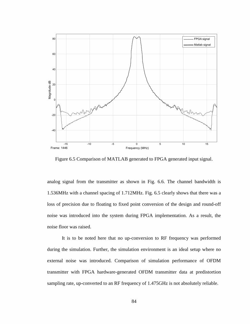
84
Figure 6.5 Comparison of MATLAB generated to FPGA generated input signal.
analog signal from the transmitter as shown in Fig. 6.6. The channel bandwidth is
1.536MHz with a channel spacing of 1.712MHz. Fig. 6.5 clearly shows that there was a
loss of precision due to floating to fixed point conversion of the design and round-off
noise was introduced into the system during FPGA implementation. As a result, the
noise floor was raised.
It is to be noted here that no up-conversion to RF frequency was performed
during the simulation. Further, the simulation environment is an ideal setup where no
external noise was introduced. Comparison of simulation performance of OFDM
transmitter with FPGA hardware-generated OFDM transmitter data at predistortion
sampling rate, up-converted to an RF frequency of 1.475GHz is not absolutely reliable.
85
Figure 6.6 Signal from OFDM transmitter at RF 1.475GHz.
This is because the hardware used to set up the transmission path and their
interconnections introduces significant noise in the system. Further, the characteristics
of analog components change with physical conditions such as heat etc., this is
unaccounted for in simulation results. Figure 6.6 shows the results of hardware
implementation of OFDM transmitter using Xilinx Virtex-4 FPGA and subsequent up-
conversion to RF using hardware described in Section 6.1 of this Chapter.
As discussed in Section 6.1, the OFDM transmitter design was re-generated at
33.33MSPS instead of 34.4176MSPS to match the system clock rate of 33.33MHz.
Therefore, the channel bandwidth and the channel spacing were altered in the same ratio
86
of 1: 0.9684. These channel parameters were changed to 1.487MHz and 1.657MHz.
The altering of these parameters to facilitate hardware implementation of the system
had negligible effects on the functional characteristics of the system. Figure 6.6 is a
capture of the Agilent 8564EC power spectrum analyzer. The spectrum shown in the
figure is the power spectrum at the output of the direct quadrature modulator evaluation
board AD8349.
Comparing the fixed point OFDM transmitter output signal spectrum in Figure
6.5 with Figure 6.6, it is seen that the carrier-to-noise ratio has increased from -100dB
to -60dB. The round-off noise added to the system when the 16-bit data is converted to
14-bit input to the DACs, the noise added from the hardware circuit performing single-
to-differential conversion of input I/Q data and also the noise from quadrature
modulator gain imperfections contribute to this noise level. Further, the
interconnections between different hardware also contribute to the total noise in the
system. It was expected that the performance of the linearizer would be affected by this
system noise and in Chapter 7 some suggestions to reduce this noise level will be
suggested.
6.2.2 Power Amplifier Performance without and with Linearization
The results of simulation of the PA performance with and without DPD
linearization for OFDM transmission has been shown in Fig. 5.3 of Chapter 5. In this
section the hardware implementation results of PA performance without and with DPD
linearization is presented. Figure 6.7 shows the results without linearizer compensation
and Fig. 6.8 shows the results of using DPD linearizer for compensation of the
nonlinear characteristics of the test PA.
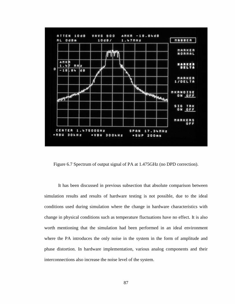
87
Figure 6.7 Spectrum of output signal of PA at 1.475GHz (no DPD correction).
It has been discussed in previous subsection that absolute comparison between
simulation results and results of hardware testing is not possible, due to the ideal
conditions used during simulation where the change in hardware characteristics with
change in physical conditions such as temperature fluctuations have no effect. It is also
worth mentioning that the simulation had been performed in an ideal environment
where the PA introduces the only noise in the system in the form of amplitude and
phase distortion. In hardware implementation, various analog components and their
interconnections also increase the noise level of the system.
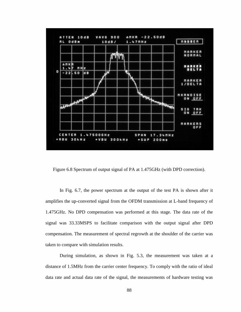
88
Figure 6.8 Spectrum of output signal of PA at 1.475GHz (with DPD correction).
In Fig. 6.7, the power spectrum at the output of the test PA is shown after it
amplifies the up-converted signal from the OFDM transmission at L-band frequency of
1.475GHz. No DPD compensation was performed at this stage. The data rate of the
signal was 33.33MSPS to facilitate comparison with the output signal after DPD
compensation. The measurement of spectral regrowth at the shoulder of the carrier was
taken to compare with simulation results.
During simulation, as shown in Fig. 5.3, the measurement was taken at a
distance of 1.5MHz from the carrier center frequency. To comply with the ratio of ideal
data rate and actual data rate of the signal, the measurements of hardware testing was
89
taken at a distance of 1.47MHz from the carrier center frequency at 1.475GHz. The
total power of the input signal maintained around -8dBm to -9dBm and care was taken
not to drive the PA into saturation. A relative power measurement between the carrier
center frequency and at 1.47MHz frequency from the carrier center frequency was used
to measure the spectral regrowth. The reduction in spectral regrowth at that fixed
distance from the carrier was sufficient to evaluate the correction performed by the
DPD linearizer system.
Figure 6.7 shows that the measurement taken at 1.47MHz from carrier shows a
spectral regrowth of -18.84dB relative to the carrier. Figure 6.8 shows the output
spectrum of the PA after DPD linearizer has performed correction. The number of
spectral averages, the sweep time and other parameters required by the PSA for
measurement was kept unchanged as in Fig. 6.8 to allow direct comparison. In Fig. 6.9,
it is clearly shown that the spectral regrowth at 1.47MHz from the carrier has been
reduced to -22.5dB. Therefore, reduction in spectral regrowth was achieved and the
performance of the L-band test PA has been improved after nonlinearity compensation
by the DPD linearizer system.
The simulation results showed a spectral regrowth reduction of 11dB was
achieved but the hardware implementation was able to achieve only 3.5-4dB correction.
As discussed in previous section, the reduction in performance of the DPD linearizer
can be attributed to the increase in noise level of the transmitter system as shown in Fig.
6.6. Further, significant amount of noise was added to the feedback path by the direct
quadrature demodulator down-conversion and also the quantization noise of the A/D
conversion performed by the ADCs cannot be ignored. It is also to be noted that
90
attenuation of RF signal level was performed in the feedback path at various stages in
an attempt to reduce the amount of signal distortion added by the quadrature
demodulator. This further increased the carrier-to-noise ratio, affecting the linearizer
performance.
6.2.3 FPGA Resource Utilization
The main design logic developed and implemented in this research used Xilinx
Virtex-4 XC4VSX35 FPGA available as a part of Nallatech XtremeDSP Development
Kit-IV evaluation board. The resource utilization is divided into 3 portions: OFDM
transmitter module, transmitter with upsampling module and DPD module. The
complete resource utilization is given in Table 6.2.
The resource utilization table shows that the complete design uses only 35% of
the available resources on the Virtex-4 FPGA. This would allow further signal
processing exploration in the future or the use of smaller devices to reduce cost of
implementation even further. The ETSI-SDR OFDM transmitter only uses 13% of the
available resources which shows that it is possible to implement radio standards based
on software-defined-radio concept on small FPGA devices. It was observed that the
Xilinx FFT/IFFT IP CORE used to implement the OFDM modulator used the maximum
resources in the transmitter.
The OFDM transmitter after being interpolated to the predistortion rate
consumed 24% of the logic resources. A major portion of this usage can be attributed to
the cascaded interpolating filters that used 23% of the available DSP48 logic slices. The
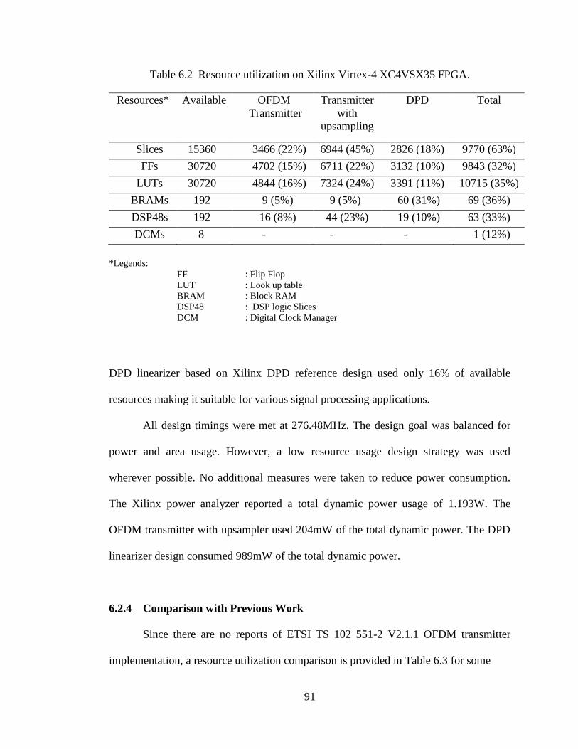
91
Table 6.2 Resource utilization on Xilinx Virtex-4 XC4VSX35 FPGA.
Resources* Available OFDM
Transmitter
Transmitter
with
upsampling
DPD Total
Slices 15360 3466 (22%) 6944 (45%) 2826 (18%) 9770 (63%)
FFs 30720 4702 (15%) 6711 (22%) 3132 (10%) 9843 (32%)
LUTs 30720 4844 (16%) 7324 (24%) 3391 (11%) 10715 (35%)
BRAMs 192 9 (5%) 9 (5%) 60 (31%) 69 (36%)
DSP48s 192 16 (8%) 44 (23%) 19 (10%) 63 (33%)
DCMs 8 - - - 1 (12%)
*Legends:
FF : Flip Flop
LUT : Look up table
BRAM : Block RAM
DSP48 : DSP logic Slices
DCM : Digital Clock Manager
DPD linearizer based on Xilinx DPD reference design used only 16% of available
resources making it suitable for various signal processing applications.
All design timings were met at 276.48MHz. The design goal was balanced for
power and area usage. However, a low resource usage design strategy was used
wherever possible. No additional measures were taken to reduce power consumption.
The Xilinx power analyzer reported a total dynamic power usage of 1.193W. The
OFDM transmitter with upsampler used 204mW of the total dynamic power. The DPD
linearizer design consumed 989mW of the total dynamic power.
6.2.4 Comparison with Previous Work
Since there are no reports of ETSI TS 102 551-2 V2.1.1 OFDM transmitter
implementation, a resource utilization comparison is provided in Table 6.3 for some

92
Table 6.3 OFDM transmitter resource usage comparison of [11], [12] and this work.
Resource [11] [12] This work
Slices 3568 2614 3466
FFs 3581 3566 4702
LUTs 6048 4304 4844
LUTs as
RAM
820 - -
BRAMs - 12 9
DSP48s - - 16
Mult 18x18 8 - -
DCMs 1 - 1
*Legends:
FF : Flip Flop
LUT : Look up table
BRAM : Block RAM
DSP48 : DSP logic Slices
DCM : Digital Clock Manager
Mult 18x18 : 18x18 Multipliers
similar work based on IEEE802.11a [11] and IEEE802.16 standard [12]. It is to be
noted that absolute comparison is not possible because the standards used in [11] and
[12] are different from this work and the design methodology is different in [11]. A pure
VHDL based approach has been used in [11] and modulation schemes such as BPSK,
QPSK and 16QAM and 64QAM has been used for OFDM transmitter with 64-point
FFT and sampling frequency of 20MHz. A Xilinx System Generator based approach
similar to this design has been used in [12] and an OFDM modulator with 256-point
FFT with QAM or QPSK modulation has been described. The comparison with other
works related to FPGA implementation of OFDM transmitters using different standards
shows that this work using ETSI-SDR standard is equally suitable for FPGA
implementation because of low resource usage, flexibility and easy transportability of
93
the design to various FPGAs.
Klymyshyn‟s thesis [6] using adaptive polynomial predistortion linearization
method using analog predistorters has been used as a reference in this work. Although,
the design methodology is incomparable and the goals and objectives of the two studies
are significantly different, both projects were sponsored by TRLABS, Saskatoon,
Canada. Therefore, it is interesting to compare the two linearizers. Figure 6.9 has been
reprinted from Klymyshyn‟s thesis. The Figure shows input power spectrum and also
output power spectrum of a PA with and without predistortion.
In [6] a filtered QPSK modulated signal was used as an input to a PA with added
phase distortion. The linearization performance was tested at IF frequency and no RF
up-conversion was performed. Improvement in spectral spreading between 7dB and
10dB was reported for the test amplifier with added phase distortion. No reports have
been provided for improvement of amplitude distortion using QPSK modulated signal.
In this work, OFDM transmitter signal instead of QPSK modulated signal was used as
an input to a test PA at an RF frequency.
It is to be noted that a comparison between distortion characteristics of QPSK
modulated signal and that of OFDM transmitter data is not accurate because OFDM
transmitter data is significantly distorted by the PA as compared to the QPSK signal
because of the high PAPR of the OFDM transmission signal. The PA used in this
research exibited both amplitude and phase distortion in L-band frequency operation. A
reduction in spectral regrowth of 11dB was possible with simulation although the
system noise from hardware implementation limited the correction to 4dB.
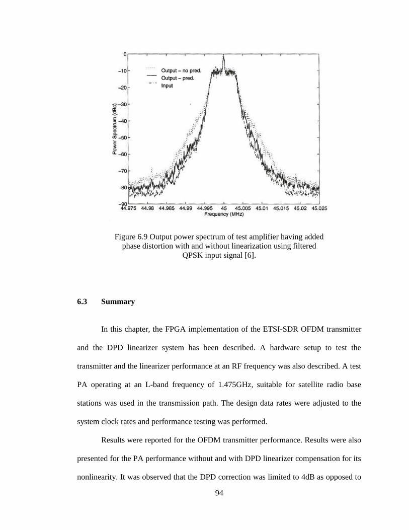
94
Figure 6.9 Output power spectrum of test amplifier having added
phase distortion with and without linearization using filtered
QPSK input signal [6].
6.3 Summary
In this chapter, the FPGA implementation of the ETSI-SDR OFDM transmitter
and the DPD linearizer system has been described. A hardware setup to test the
transmitter and the linearizer performance at an RF frequency was also described. A test
PA operating at an L-band frequency of 1.475GHz, suitable for satellite radio base
stations was used in the transmission path. The design data rates were adjusted to the
system clock rates and performance testing was performed.
Results were reported for the OFDM transmitter performance. Results were also
presented for the PA performance without and with DPD linearizer compensation for its
nonlinearity. It was observed that the DPD correction was limited to 4dB as opposed to

95
a correction of 11dB during simulation. This was attributed to the added system noise
during hardware implementation.
A summary of logic resource utilization and power consumption of the design
on Xilinx Virtex-4 FPGA was given and the results were discussed. Finally, some
previous works were compared to this work and the results were also discussed. The
following chapter concludes this thesis.
96
7. CONCLUSIONS AND FUTURE WORK
7.1 Conclusions
Many newly developed radio standards such as ETSI-SDR are still being
subjected to development and deployment. It is quite a challenging task to build a
suitable hardware platform that would have fast and intense processing capabilities,
support high data rates and also be flexible and reprogrammable. Moreover, the
hardware complexity involved in such systems can significantly increase the operational
costs. Field programmable gate array devices provide a low-cost, off-the-shelf hardware
platform for such standards. The fast processing capabilities, vast resources, easy
programmability and low cost make FPGAs a perfect platform for such complex
satellite radio systems. In this project, an OFDM transmission system model, suitable
for L-band satellite radio has been designed according to ETSI-SDR standard
specifications and implemented in FPGA. A low cost, FPGA based solution to
compensate for the nonlinear effects of power amplifiers used in such systems was
suggested, implemented and tested on hardware platform.
At first, it was shown that it is possible to model systems based on radio
standards such as ETSI-SDR, on low-cost, high-speed FPGAs, using advanced DSP
design tools. This eliminates the need for sophisticated equipments such as high quality
signal generators to create models of test systems. The OFDM system model used in
97
this research is based on standard ETSI TS 102 551-2 V2.1.1 (2007-2008) for IPL-MC
transmission Mode-3 using L-band frequency (1.450-1.490GHz).Various design
strategies and architectures were explored and finally the model was realized on Xilinx
XtremeDSP Virtex-4 FPGA platform using Xilinx System Generator for DSP design
tools. This design method offered the flexibility to be used and verified in simulation
environment such as MATLAB/SIMULINK and easy to migrate other FPGA platforms.
This design method also shows that resource usage can be minimized and design speed
can be maximized using various IP cores and advanced DSP design tools with unique
system integration capabilities.
Next, the signal distortion caused by driving the RF power amplifier to their
nonlinear region in modern digital communications, specifically satellite radio systems,
was studied. These RF power amplifiers, when driven in their nonlinear region by non-
constant envelope signals cause in-band distortion and spectral leakage in adjacent
channels. The trade-off between PA efficiency and nonlinearity is a major concern in
SDR systems, where there is a constant demand for low power consumption and high
signal quality. The PA nonlinear characteristics and their unfavorable effects on
spectrally efficient, non-constant envelope signals such as QAM were discussed in
details.
Another significant goal established in this research is finding a suitable
compensation technique for the nonlinear characteristics of PA manufactured by SED
systems, Saskatoon. Various linearization techniques that have been used in the past to
compensate for the nonlinear characteristics of RF power amplifiers transmitting non-
constant amplitude signals were reviewed. A linearizer system was designed based on a
98
state-of-the-art reference design from Xilinx based on digital predistortion. The chosen
design has been reportedly tested on signal bandwidth up to 20MHz at RF frequencies.
Therefore, it was found suitable for the signal bandwidth of 1.5314MHz used in this
project at 1.475GHz carrier frequency.
The fourth goal set for this research was to test the functionality of the ETSI-
SDR OFDM transmitter and the PA performance with and without DPD linearizer
compensation. A simulation model of the test system was developed in an integrated
environment of MATLAB/SIMULINK and Xilinx System Generator. A simulation
equivalent of the PA was modeled as a memory-less polynomial from the
experimentally obtained AM-AM and AM-PM characteristics data. The PA output
without and with DPD compensation were measured and compared. No RF frequency
up-conversion was performed in this simulation environment. A spectral regrowth
suppression of 11dB was observed at a frequency of 1.5MHz from the carrier. This was
expected nonlinearity correction under ideal conditions.
Finally, the complete system was successfully implemented in hardware. The
OFDM transmission system and the DPD linearizer module were completely contained
in the Xilinx Virtex-4 FPGA. Timing was met at 276.48MHz. The baseband filtering,
RF up-conversion and down-conversion were performed in analog domain. The test PA
operating at an L-band RF of 1.475GHz was used in the analog chain. A spectral
regrowth suppression of 3.66dB was observed at 1.47MHz from carrier frequency of
1.475GHz as opposed to expected 6-9dB. It was concluded that the DPD linearizer
performance was compromised by the limited capabilities of the built-in A/D and D/A
99
converters on the FPGA evaluation kit, combined noise of various components in the
analog chain and signal attenuation in the RF feedback path.
7.2 Future Work
The work done so far in this SED Systems/TRLABS project has a potential of
being used as a foundation of an industrial project of significant commercial value.
Some improvements are beyond the scope of this research and listed as suggested future
work as follows:
1. The OFDM transmission model used is this system is based on ETSI–SDR
standard ETSI TS 102 551-2 V2.1.1 (2007-2008), Mode-3 using OFDM with 1k IFFT
in 1.712MHz channel spacing. The other Modes in this Standard are left for future
work. Also, the flexibility of the design method used in this research would allow
explorations of other new radio standards of increased complexity.
2. The 14-bit A/D and D/A converters used in this research are built-in
components of the Xilinx XtremeDSP Virtex-4 FPGA evaluation kit. The A/D and D/A
converters reduce the dynamic range of the 16-bit signal used by the DPD linearizer. It
can be expected that using 16-bit converters would improve linearizer performance.
3. Further improvements in linearizer performance can be expected by using
custom built hardware for RF up-converting and down-converting mixers. For the
purpose of this research, evaluation boards from Analog Devices and Linear
Technology were used, which perform optimally for a limited range of frequency. At
the operating RF of this project those boards added noise to the system. The DPD
linearizer also has the capability to compensate for direct RF up-converter gain
100
imperfections [32-34], which has not been utilized in this research. The design performs
RF up-converter imperfections correction only when the down-converting mixer
operates at a frequency different from the RF up-converter and the signal is down-
converted to IF frequency. In this research, direct RF up-conversion and down-
conversion have been performed on baseband I/Q signals, therefore the DPD module
failed to detect the RF up-conversion imperfections comparing the up-converted and
down-converted signals and therefore no corrections were performed.
4. Another suggested improvement is reducing the peak-to-average-power-ratio
(PAPR) of the input signal. One of the problems in OFDM transmission is high Crest
Factor or PAPR, caused by addition of large number of independently modulated sub-
carriers in parallel at the transmitter. These may add up to a very high instantaneous
peak compared to the average signal power. High PAPR is associated with increased
signal distortion. This research focuses on DPD linearizer performance and therefore no
attempts have been made to reduce the PAPR of the input signal. The results from
performance testing in [32-34] show that a significant improvement in DPD
performance was achieved when used in conjunction with Xilinx crest-factor-reduction
(CFR) reference design module.
5. The OFDM receiver system performing demodulation of the transmitted data
was not included in research. Therefore, no comparison of error vector magnitude
(EVM) of transmitted and received data was performed for the given ETSI-SDR
standard implementation. This option is open to future exploration.
101
REFERENCES
[1] K. Raghunandan. “Satellite digital radio brings new image to broadcasting.” in
IEEE Proceedings of 2nd International Conference on recent advances in Space
Technologies, Jun. 2005, pp. 799-804.
[2] B. Cuesta, I. Moreno, A. Yun and J. Rodriguez. “Analysis of the Convergence
between DVB-SH and ETSI-SDR.” in IEEE Proceedings of First International
Conference on Advances in Satellite and Space Communications, Jul. 2009,pp.
13-18.
[3] “Satellite Radio.” Available: www.en.wikipedia.org/wiki/Satellite_radio
[Accessed: Mar. 2010].
[4] “ETSI Satellite Digital Radio.” Available:
www.en.wikipedia.org/wiki/ETSI_Satellite_Digital_Radio [Accessed: Mar.
2010].
[5] M. Hella and M. Ismail. RF CMOS Power Amplifiers: Theory, Design,
Implementation. USA: Kluwer Academic Publishers, 2002.
[6] D.M. Klymyshyn. “A Power Amplifier Linearizer using Adaptive Polynomial
Predistortion.” M.Sc. thesis, University of Saskatchewan, Canada, 1995.
[7] M. Ghadheri. “Adaptive Linearization of Efficient High Power Amplifiers using
Polynomial Predistortion with Global Optimization.” Ph.D. thesis, University of
Saskatchewan, Canada, 1995.
[8] M. Serra, J. Ordiex, P. Marti and J. Carrabina. “OFDM Demonstrator:
Transmitter,” presented at the 7th
International OFDM Workshop, Germany,
Sep. 2002.
[9] C. Dick and F. Harris. “FPGA implementation of an OFDM PHY.” Signals,
Systems and Computers, 2003: Conference Record of the 37th
Asilomer
Conference, vol. 1, pp. 905- 909, Nov. 2003.
[10] A. Sghaier, S. Areibi, and R. Dony. “IEEE802.16-2004 OFDM functions
implementation on FPGAs with design exploration.” in FPL.2008: Proceedings
of the 2008 International Conference on Field Programmable Logic and
Applications, Sep. 2008, pp. 519-522.

102
[11] A. Sghaier, S. Areibi, and B. Dony. “A Pipelined Implementation of OFDM
Transmission on Reconfigurable Platforms.” in CCECE 2008: Proeedings of the
2008 Canadian Conference on Electrical and Computer Engineering, May
2008, pp. 801-804.
[12] J. Garcia and R. Cumplido. “On the design of an FPGA-based OFDM modulator
for IEEE 802.16-2004,” presented at the RECONFIGURE‟05: 2005
International Conference on Reconfigurable Computing and FPGAs, Puebla,
Mexico, Sep. 2005.
[13] L. Hanzo and T. Keller. OFDM and MC-CDMA: A Primer. UK: John Wiley &
Sons Inc., 2006.
[14] Fuqin Xiong. Digital Modulation Techniques. USA: Artech House Inc., 2006.
[15] R. Marsalek, P. Jardin and G. Baudion. “From Post-Distortion to Pre-Distortion
for Power Amplifier Linearization.” IEEE Communications Letters, vol.7, pp.
308-310, Jul. 2003.
[16] R. Marsalek, P. Jardin and G. Baudion. “Power Amplifier Linearization Using
Pre-distortion with Memory.” in 13th
International Czech-Slovak Scientific
Conference RADIOELEKTRONIKA, 2003, pp. 193-196.
[17] S. Cripps. RF Power Amplifiers for Wireless Communications. USA : Artech
House Inc., Academic Publishers, March 1999.
[18] S. Bruss. Class Lecture, Topic: “Linearization Methods.” Department of
Electrical and Computer Engineering, University of California, Davis, April
2003.
[19] J. P. Moffatt and J. P MacEachern. “An adaptive QAM linearizer using
Postdistortion.” in IEEE Global Telecommunications Conference, Nov. 1989,
pp. 406- 412.
[20] L. D. Quach and S. P Stapleton. “A postdistortion receiver for mobile
communications.” IEEE Transactions on Vehicular Technology, vol. 42, pp.
604- 616, Nov. 1993.
[21] L. D. Quach and S. P Stapleton. “Reduction of adjacent channel interference
using postdistortion.” IEEE 42nd
Vehicular Technology Conference, vol. 2, pp.
915- 918, May 1992.
[22] T. M. Nguyen, J. Yoh, C. H. Lee, H. T. Tran and D. M. Johnson. “Modeling of
HPA and HPA linearization through a predistorter: Global Broadcasting Service
applications.” IEEE Transactions on Broadcasting, vol. 49, pp. 132-141, 2003.
103
[23] S. P Stapleton, G. S. Kandola and J. K.Cavers. “Simulation and Analysis of an
Adaptive Predistorter Utilizing a Complex Spectral Convolution.” IEEE
Tranactions on Vehicular Technology, vol. 41, pp. 387-394, Nov. 1992.
[24] J. K. Cavers. “Amplifier Linearisation Using a Digital Predistortion with Fast
Adaptation and Low Memory Requirements.” IEEE Transactions on Vehicular
Technology Conference, vol. 39, pp. 374-382, Nov. 1990.
[25] H. Bebes and T. Le-Ngoc. “A Fast Adaptive Predistorter for Nonlinearly
Amplified M-QAM Signals.” IEEE Proceedings of the Global Comunications
Conference, vol. 1, pp. 108-112, Nov. 2000.
[26] N. Safari, J. P. Tanem and T. Roste. “Block based Predistortion for Amplifier
Linearization in Burst type Mobile Satellite Communications.” IEEE
Proceedings of 35th
European Microwave Conference, vol. 3, pp.1783-1786,
2005.
[27] N. Ceylan, J.E. Mueller, T. Pittorino and R. Weigel. “Mobile Phone Power
Amplifier Linearity and Efficiency Enhancement using Digital Predistortion.”
IEEE Proceedings of 33rd European Microwave Conference, vol. 1, pp. 269-
272, Oct. 2003.
[28] A. Benchahed, A. Ghazel, M. Mabrouk, C. Rebai and M.F. Ghannouchi. “RF
Digital Predistorter for Power Amplifiers of 3G Base Stations.” in IEEE
Proceedings of 13th International Conference on Electronics, Circuits and
Systems, Dec. 2006, pp. 999-1002.
[29] M. Franco, A. Guida, A. Katz and P. Herczfeld. “Reduction of In-Band
Intermodulation Distortion Products in Radio Frequency Power Amplifiers with
Digital Predistortion Linearization.” in IEEE Proceedings of International
Microwave Symposium Digest, Jun. 2006, pp. 918 – 921.
[30] N. Lashkarian and C. Dick. “FPGA Implementation of Digital Predistortion
Linearizers for Wideband Power Amplifiers,” presented at the SDR‟04: 2004
Technical Conference and Product Exposition, Phoenix, USA, Nov. 2004.
[31] F. Antonio, W. Hamdy, P. Heidmann, J. Heizer, N. Kasturi, D.P. Oses and C.
Riddle. “A Novel Adaptive Predistortion Technique for Power Amplifiers.”
IEEE Proceedings Conference on Vehicular Technology, vol. 2, pp.1505 -1509,
May 1999.
[32] S. Summerfield, H. Parekh and V. Barnes. Digital Predistortion Reference
Design, Application Note XAPP1044 (v1.0.1). USA: Xilinx Inc., Apr. 21, 2008.
[33] S. Summerfield, H. Parekh and V. Barnes. Digital Predistortion Reference
Design V2.0, EA2 Release Note. USA: Xilinx Inc., Oct. 31, 2008.
104
[34] S. Summerfield, H. Parekh and V. Barnes. Digital Predistortion V2.0,
Application Note XAPP1128 (v1.0). USA: Xilinx Inc., Mar. 18, 2009.
[35] Xilinx Inc. Xilinx Digital Pre- Distortion Reference Design (DPD) V2.0.
Available: www.xilinx.com/publications/prod_mktg/pn2061.pdf [Accessed: Jun.
2009].
[36] European Telecommunications Standards Institute (ETSI). “Satellite Earth
Stations and Systems; Satellite Digital Radio (SDR) Systems; Inner Physical
layer of the Radio Interface; Part 2: Multiple Carrier Transmission.” ETSI TS
102 551-2 V2.1.1 (2007-2008), Aug. 2007.
[37] The Mathworks. MATLAB R2007a User’s Guide. Version 7.4 (R2007a), 2007.
[38] Xilinx Inc. System Generator for DSP User Guide. Release 10.1. Available:
www.xilinx.com/support/sw_manuals/sysgen_user.pdf [Accessed: Jun. 2010].
[39] Xilinx Inc. Linear Feedback Shift Register LogiCORE v3.0 Datasheet. USA:
Xilinx Inc., 2003.
[40] J. Proakis and D. Manolakis. Digital Signal Processing: Principles, Algorithms
and Applications. USA: Prentice Hall, 2007.
[41] Xilinx Inc. Fast Fourier Transform LogiCORE v5.0 Datasheet. USA: Xilinx
Inc., 2008.
[42] L. Milic. Multirate Filtering for Digital Signal Processing: MATLAB
Applications. USA: IGI Global, 2009.
[43] Nallatech Ltd. XtremeDSP Development Kit-IV User Guide. USA: Nallatech
Ltd., 2005.
[44] Xilinx Inc. Virtex-4 FPGA User Guide. Available:
www.xilinx.com/support/documentation/user_guides/ug070.pdf [Accessed: Jan.
2010].
[45] Mini Circuits. IF/RF Microwave Signal Processing Components Guide. USA:
Mini Circuits, 2007.
[46] Analog Devices Inc. 700MHz to 2700MHz Quadrature Modulator AD8349
Datasheet. USA: Analog Devices Inc., 2005.
[47] CREE Inc. CRF24060, 60W, 2.0GHz, SiC MESFET, Cree Wireless
Device Datasheet. Available: www.cree.com/products/pdf/CRF24060.pdf
[Accessed: May 2010].

105
[48] CREE Inc. CRF24010, 10W, 2.4GHz, SiC MESFET, Cree Wireless
Device Datasheet. Available: www.cree.com/products/pdf/CRF24010.pdf
[Accessed: May 2010].
[49] Linear Technology Corporation. 800MHz to 2.7GHz High Linearity Direct
Conversion Quadrature Demodulator LT5575 Datasheet, USA: Linear
Technology Corporation, 2007.

106
APPENDIX A
4-BIT PSEUDO RANDOM BINARY SEQUENCE GENERATOR
The pseudo random binary sequence (PRBS) generator designed in this work is
shown in Fig. A.1.The design uses four linear feedback shift registers (LFSR) in
parallel. The LFSRs are of Galois type and consist of 21, 20, 17 and 18 bits
respectively. A 3-bit Galois type LFSR with tap locations at 0 and 2 is shown in
Fig.A.2. The polynomials equations and the feedback the tap location of the LFSRs are
given in Table A. The generated sequence is of length 2LFSR-SIZE
-1. The output of each
LFSR was generated serially. The outputs of the LFSRs were concatenated to form a 4-
bit output.
The output sequences were fed to a scrambler block (Black Box module) to
maximize the length of the generated sequence. The output of the scrambler was
obtained as a sequence of random numbers.
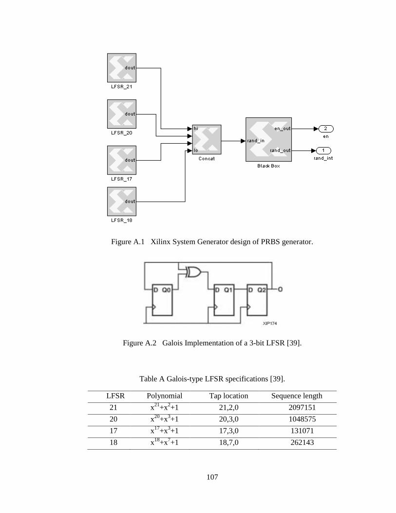
107
Figure A.1 Xilinx System Generator design of PRBS generator.
Figure A.2 Galois Implementation of a 3-bit LFSR [39].
Table A Galois-type LFSR specifications [39].
LFSR
Size
Polynomial Tap location Sequence length
21 x21
+x2+1 21,2,0 2097151
20 x20
+x3+1 20,3,0 1048575
17 x17
+x3+1 17,3,0 131071
18 x18
+x7+1 18,7,0 262143
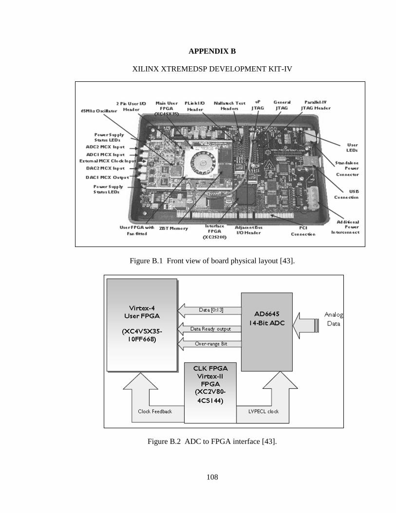
108
APPENDIX B
XILINX XTREMEDSP DEVELOPMENT KIT-IV
Figure B.1 Front view of board physical layout [43].
Figure B.2 ADC to FPGA interface [43].
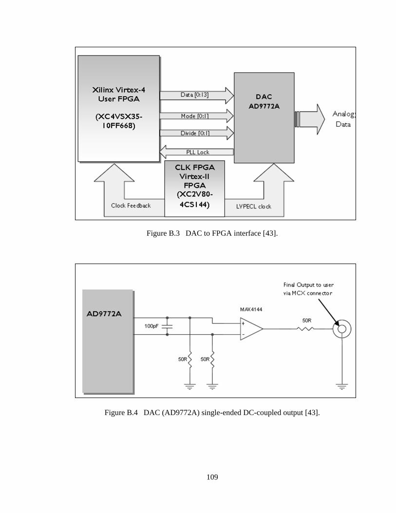
109
Figure B.3 DAC to FPGA interface [43].
Figure B.4 DAC (AD9772A) single-ended DC-coupled output [43].

110
APPENDIX C
INTERFACE OF DIFFERENTIAL AMPLIFIER AD8132 AND
QUADRATURE MODULATOR AD8349
Figure C Single-to-differential conversion of signal with 400mV DC bias addition [46].
Top Related