


Languages
Pages
Legal


University of South Carolina University of South Carolina
Scholar Commons Scholar Commons
Theses and Dissertations
2015
Defect Characterization of 4H-SIC by Deep Level Transient Defect Characterization of 4H-SIC by Deep Level Transient
Spectroscopy (DLTS) and Influence of Defects on Device Spectroscopy (DLTS) and Influence of Defects on Device
Performance Performance
Mohammad Abdul Mannan University of South Carolina - Columbia
Follow this and additional works at: https://scholarcommons.sc.edu/etd
Part of the Electrical and Computer Engineering Commons
Recommended Citation Recommended Citation Mannan, M. A.(2015). Defect Characterization of 4H-SIC by Deep Level Transient Spectroscopy (DLTS) and Influence of Defects on Device Performance. (Doctoral dissertation). Retrieved from https://scholarcommons.sc.edu/etd/3083
This Open Access Dissertation is brought to you by Scholar Commons. It has been accepted for inclusion in Theses and Dissertations by an authorized administrator of Scholar Commons. For more information, please contact [email protected].

DEFECT CHARACTERIZATION OF 4H-SIC BY DEEP LEVEL TRANSIENT
SPECTROSCOPY (DLTS) AND INFLUENCE OF DEFECTS ON DEVICE
PERFORMANCE
by
Mohammad Abdul Mannan
Bachelor of Science
Bangladesh University of Engineering and Technology, 1998
Master of Science
Concordia University, 2011
Submitted in Partial Fulfillment of the Requirements
For the Degree of Doctor of Philosophy in
Electrical Engineering
College of Engineering and Computing
University of South Carolina
2015
Accepted by:
Krishna C. Mandal, Major Professor
Yinchao Chen, Committee Member
Guoan Wang, Committee Member
Fanglin Chen, Committee Member
Lacy Ford, Vice Provost and Dean of Graduate Studies

ii
© Copyright by Mohammad Abdul Mannan, 2015
All Rights Reserved.

iii
DEDICATION
This dissertation is dedicated to my wife Farhana Anjum, my daughter Fabliha Maliyat
and my son Fawaz Mustaneer, whose relentless encouragement and support during this
extraordinary odyssey has helped me to put my best efforts toward this research work.

iv
ACKNOWLEDGEMENTS
Firstly, I would like to thank my advisor, Dr. Krishna C. Mandal, for his
continued support and guidance on this research. My development within his group has
allowed me to undertake this work with the proper knowledge and skillset. I would also
like to thank my committee members, Dr. Yinchao Chen, Dr. Guoan Wang, and Dr.
Fanglin Chen, for taking the time to oversee my research and their support of my work.
I would also like to thank the following people for their contributions to the
research performed in this work:
Khai Nguyen, who assisted heavily to set up take Alpha Spectrometer and taking
Spectroscopy measurement.
Dr. Sandeep K. Chaudhuri (Electrical Engineering, University of South Carolina)
for his assistance during the set-up of the DLTS equipment.
The staff of Electron Microscopy Center (EMC) at the University of South
Carolina for their assistance with Scanning Electron Microscopy (SEM) and
Energy Dispersive X-ray Spectroscopy (EDX) studies.
Dr. Shuguo Ma (College of Engineering and Computing, University of South
Carolina) for performing the XPS characterization.

v
I would also like to thank my fellow lab members, Ramesh Krishna, Sandip Das,
Kelvin Zavalla, Rahmi Pak, and Cihan Oner for their support and friendship throughout
this process. Finally, I would like to thank all those faculty members and staff in the
Electrical Engineering department at the University of South Carolina whose cumulative
efforts have contributed to the successful completion of my doctoral research. Without
their contributions, this work would have been impossible to perform.

vi
ABSTRACT
Silicon carbide (SiC) is one of the key materials for high power opto-electronic
devices due to its superior material properties over conventional semiconductors (e.g., Si,
Ge, GaAs, etc). SiC is also very stable and a highly suitable material for radiation
detection at room temperature and above. The availability of detector grade single
crystalline bulk SiC is limited by the existing crystal growth techniques which introduce
extended and microscopic crystallographic defects during the growth process. Recently,
SiC based high-resolution semiconductor detectors for ionizing radiation have attracted
world-wide attention due to the availability of high resistive, highly crystalline epitaxial
layers with very low micropipe defect content (< 1 cm-2
). SiC Schottky barrier radiation
detectors on epitaxial layers can be operated with a high signal-to-noise ratio even above
room temperature due to its wide band-gap. However, significant amount of intrinsic
defects and impurities still exist in the grown SiC epilayer which may act as traps or
recombination/generation centers and can lead to increased leakage current, poor carrier
lifetime, and reduced carrier mobility. Unfortunately, the nature of these electrically
active deep levels and their behavior are not well understood. Therefore, it is extremely
important to identify these electrically active defects present in the grown epitaxial layers
and to understand how they affect the detector performance in terms of leakage current
and energy resolution.
vii
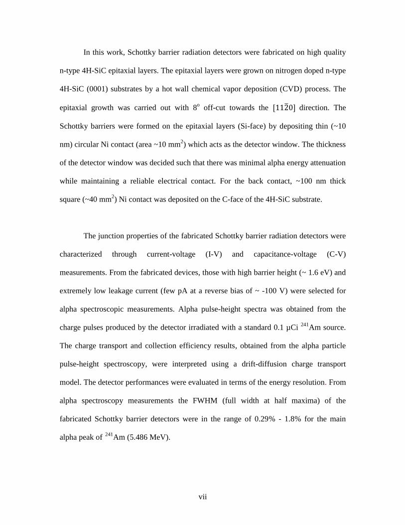
In this work, Schottky barrier radiation detectors were fabricated on high quality
n-type 4H-SiC epitaxial layers. The epitaxial layers were grown on nitrogen doped n-type
4H-SiC (0001) substrates by a hot wall chemical vapor deposition (CVD) process. The
epitaxial growth was carried out with 8o off-cut towards the [112̅0]
direction. The
Schottky barriers were formed on the epitaxial layers (Si-face) by depositing thin (~10
nm) circular Ni contact (area ~10 mm2) which acts as the detector window. The thickness
of the detector window was decided such that there was minimal alpha energy attenuation
while maintaining a reliable electrical contact. For the back contact, ~100 nm thick
square (~40 mm2) Ni contact was deposited on the C-face of the 4H-SiC substrate.
The junction properties of the fabricated Schottky barrier radiation detectors were
characterized through current-voltage (I-V) and capacitance-voltage (C-V)
measurements. From the fabricated devices, those with high barrier height (~ 1.6 eV) and
extremely low leakage current (few pA at a reverse bias of ~ -100 V) were selected for
alpha spectroscopic measurements. Alpha pulse-height spectra was obtained from the
charge pulses produced by the detector irradiated with a standard 0.1 µCi 241
Am source.
The charge transport and collection efficiency results, obtained from the alpha particle
pulse-height spectroscopy, were interpreted using a drift-diffusion charge transport
model. The detector performances were evaluated in terms of the energy resolution. From
alpha spectroscopy measurements the FWHM (full width at half maxima) of the
fabricated Schottky barrier detectors were in the range of 0.29% - 1.8% for the main
alpha peak of 241
Am (5.486 MeV).

viii
Deep level transient spectroscopy (DLTS) studies were conducted in the
temperature range of 80 K - 800 K to identify and characterize the electrically active
defects present in the epitaxial layers. Deep level defect parameters (i.e. activation
energy, capture cross-section, and density) were calculated from the Arrhenius plots
which were obtained from the DLTS spectra at different rate windows. The observed
defects in various epitaxial layers were identified and compared with the literature. In the
50 µm epitaxial layer, a new defect level located at Ec - 2.4 eV was observed for the first
time. The differences in the performance of different detectors were correlated on the
basis of the barrier properties and the deep level defect types, concentrations, and capture
cross-sections. It was found that detectors, fabricated on similar wafers, can perform in a
substantially different manner depending on the defect types. For 20 µm epitaxial layer
Schottky barrier radiation detectors, deep levels Z1/2 (located at ~ Ec - 0.6 eV) and EH6/7
(located at ~ Ec - 1.6 eV) are related to carbon vacancies and their complexes which
mostly affect the detector resolution. For 50 µm epitaxial layer Schottky barrier radiation
detectors, Z1/2, EH5, and the newly identified defect located at Ec - 2.4 eV mostly affect
the detector resolution.
The annealing behavior of deep level defects was thoroughly investigated by
systematic C-DLTS measurements before and after isochronal annealing in the
temperature range of 100 ˚C - 800 ˚C. Defect parameters were calculated after each
isochronal annealing. Capture cross-sections and densities for all the defects were
investigated to analyze the impact of annealing. The capture cross-sections of the defects
Ti (c) (located at Ec ˗ 0.17 eV) and EH5 (located at Ec ˗ 1.03 eV) were observed to

ix
decrease with annealing temperature while the densities did not change significantly.
Deep level defects Z1/2 and EH6/7 were found to be stable up to the annealing temperature
of 800 ˚C.
.

x
TABLE OF CONTENTS
DEDICATION.................................................................................................................. iii
ACKNOWLEDGEMENTS ............................................................................................ iv
ABSTRACT ...................................................................................................................... vi
LIST OF TABLES .......................................................................................................... xii
LIST OF FIGURES ....................................................................................................... xiii
LIST OF ABBREVIATIONS ..................................................................................... xviii
CHAPTER 1: GENERAL INTRODUCTION ............................................................... 1
1.1 DISSERTATION INTRODUCTION ................................................................................ 1
1.2 DISSERTATION OVERVIEW........................................................................................ 4
CHAPTER 2: SIC: PROPERTIES AND ELECTRONIC DEVICES ......................... 6
2.1 SIC MATERIAL PROPERTIES ..................................................................................... 6
2.2 SIC CRYSTAL GROWTH............................................................................................ 8
2.3 THEORETICAL BACKGROUND METAL-SEMICONDUCTOR CONTACT ....................... 12
2.4 CONCLUSION .......................................................................................................... 25
CHAPTER 3: DEFECTS IN SIC .................................................................................. 26
3.1 OVERVIEW ............................................................................................................. 26
3.2 POINT DEFECTS ...................................................................................................... 26
3.3 MORPHOLOGICAL DEFECTS ................................................................................... 27
3.4 MORPHOLOGICAL DEFECTS DELINEATION BY ETCHING ........................................ 30
3.5 CONCLUSIONS ........................................................................................................ 35
CHAPTER 4: DETECTOR FABRICATION AND CHARACTERIZATION ........ 37
4.1 4H-SIC DETECTOR FABRICATION .......................................................................... 37

xi
4.2 ELECTRICAL CHARACTERISTICS OF FABRICATED DETECTOR ................................. 39
4.3 RADIATION INTERACTION WITH SEMICONDUCTOR MATERIALS ............................. 47
4.4 DRIFT-DIFFUSION MODEL...................................................................................... 48
4.5 RADIATION DETECTION ......................................................................................... 49
4.6 ALPHA SPECTROSCOPY MEASUREMENT RESULTS ................................................. 58
4.7 CONCLUSION .......................................................................................................... 64
CHAPTER 5: DEFECT CHARACTERIZATION BY DLTS STUDIES ................. 65
5.1 INTRODUCTION ...................................................................................................... 65
5.2 DEFECT PARAMETERS ............................................................................................ 67
5.3 DEFECT CHARACTERIZATION BY THERMALLY STIMULATED CURRENT ................. 68
5.4 THEORETICAL BACKGROUND OF DLTS MEASUREMENT ....................................... 75
5.5 DLTS EXPERIMENTAL SETUP ................................................................................ 83
5.6 DEFECTS’ ROLE ON DETECTOR PERFORMANCE ..................................................... 97
5.7 CONCLUSION ........................................................................................................ 101
CHAPTER 6: ANNEALING BEHAVIOR OF CRYSTALLINE DEFECTS ........ 102
6.1 INTRODUCTION .................................................................................................... 102
6.2 DEEP LEVEL TRANSIENT SPECTRA BEFORE ANNEALING ...................................... 102
6.3 EXPERIMENT FOR ISOCHRONAL ANNEALING STUDIES ......................................... 105
6.4 ANNEALING STUDIES RESULTS ............................................................................ 107
6.5 CONCLUSION ........................................................................................................ 125
CHAPTER 7: CONCLUSION AND SUGGESTIONS FOR FUTURE WORK .... 127
7.1 CONCLUSION ........................................................................................................ 127
7.2 FUTURE WORK .................................................................................................... 129
REFERENCES .............................................................................................................. 132

xii
LIST OF TABLES
Table 2.1. Comparisons of properties of selected important materials at 300 K [35] ........ 9
Table 4.1. I-V characteristics parameters of the Schottky detector .................................. 41
Table 5.1. Trap parameters deduced from TSC measurements [86] ................................ 72
Table 5.2. Trap parameters by TSC measurements for the 4H-SiC n-type epilayer [92] . 74
Table 5.3. Defect parameters of the deep levels for the detector AD06 ........................... 91
Table 5.4. Defect parameters of the detector AS1 obtained from the DLTS scans .......... 93
Table 5.5. Defect parameters of the detector AS2 obtained from the DLTS scans .......... 93
Table 5.6. Defect parameters of the detector AS3 obtained from the DLTS scans .......... 93
Table 5.7. Detector properties and defect parameters for the detector AS1 ..................... 99
Table 5.8. Detector properties and defect parameters for the detector AS2 ..................... 99
Table 5.9. Detector properties and defect parameters for the detector AS3 ..................... 99
Table 5.10. Detector properties and defect parameters for the detector AD06 .............. 100
Table 6.1. Defect Parameters Obtained from the DLTS Measurements. ....................... 104
Table 6.2. Defect parameters obtained after annealing at 100 ˚C ................................... 115
Table 6.3. Defect parameters after annealing at 200 ˚C ................................................. 116
Table 6.4. Defect parameters after annealing at 400 ˚C ................................................. 117
Table 6.5. Defect parameters after annealing at 600 ˚C ................................................. 118
Table 6.6. Defect parameters after obtained annealing 800 ˚C ....................................... 119

xiii
LIST OF FIGURES
Figure 2.1. Energy band diagram of metal-semiconductor Ohmic contact: (a) Metal and
n-type semiconductor; (b) Metal and p-type semiconductor. ............................... 14
Figure 2.2. Energy band diagram of metal-semiconductor Schottky contact; (a) Metal
and n-type semiconductor; (b) Metal and p-type semiconductor. ........................ 16
Figure 2.3. Transport process in a forward biased Schottky barrier ................................. 19
Figure 2.4. Linear fit of current-voltage (I-V) acquired data plotted in logarithmic scale 22
Figure 2.5. Capacitance-voltage data acquired using a Schottky diode. .......................... 23
Figure 2.6. 1/C2 vs. reverse bias plot with linear fitting. Variation of 1/C
2 as a function of
reverse bias corresponding to the C-V plot shown in above . The straight line
shows the linear fit of the experimental data. ....................................................... 25
Figure 3.1. SEM image of the molten KOH etched bulk SiC: (a) Region with TSDs and
TEDs; (b) Regions with BPDs and TEDs. ............................................................ 33
Figure 3.2. SEM images of the molten KOH etched bulk SiC: (a) Region with TSDs and
TEDs; (b) Enlarge images of micropipes; (C) ) Enlarge images of closed core and
threading edge dislocations. .................................................................................. 34
Figure 3.3. (a) SEM images of the molten KOH etched SiC epitaxial layers; (b) Enlarged
images of closed core and threading edge dislocations. ....................................... 35
Figure 4.1. Photograph of an n-type 4H-SiC epitaxial layer wafer. ................................. 37
Figure 4.2. Schematic diagram of the cross-sectional view of 50µm thick n-type 4H-SiC
Schottky barrier device. ........................................................................................ 38
Figure 4.3. Schematic of the I-V and C-V experimental setup. ........................................ 39
Figure 4.4. Photograph of the experimental setup for the I-V and C-V measurements. The
detector is mounted inside the aluminum box. ..................................................... 40
Figure 4.5. Variation of junction current as a function of applied bias for a 50 µm n-type
Ni/4H-SiC epitaxial Schottky barrier radiation detector. ..................................... 42
Figure 4.6. Forward I-V characteristics on 4H-SiC epitaxial Schottky barrier detectors
AS1, AS2, and AS3. ............................................................................................. 43

xiv
Figure 4.7. Reverse I-V characteristics obtained for 4H-SiC epitaxial Schottky barrier
detectors AS1, AS2, and AS3. .............................................................................. 44
Figure 4.8. 1/C2 vs V plot for a 50 µm n-type Ni/4H-SiC epitaxial Schottky barrier
detector. The open circles are the experimental data points and the solid line is a
straight line fit to the experimental data. Inset shows the original C-V plot. ....... 45
Figure 4.9. 1/C2 vs V plots for 4H-SiC epitaxial Schottky barrier radiation detectors AS1,
AS2, and AS3........................................................................................................ 47
Figure 4.10. Energy loss of 5.48 MeV alpha particle as a function of penetration depth. 48
Figure 4.11. Schematic diagram of an analog radiation detection measurement system. 50
Figure 4.12. (a) Simplified circuit diagram for a charge sensitive preamplifier used in a
detection system. (b) Input and output pulse shapes seen by a preamplifier [7] .. 51
Figure 4.13. (a) Typical input and output pulse shapes seen by a shaping amplifier. (b)
Simplified circuit diagram for the various stages of differentiation (CR) and
integration (RC) used by an analog shaping amplifier [81]. ................................. 52
Figure 4.14. Photograph of the 4H-SiC epitaxial Schottky barrier radiation detector inside
RFI/EMI shielded test box. ................................................................................... 53
Figure 4.15. Connection schematic for analog data acquisition set-up. ........................... 54
Figure 4.16. Schematic of the electrical connections for energy calibration. ................... 56
Figure 4.17. (a) Pulse-height spectrum obtained for six different pulse sizes, and (b)
Corresponding calibration curve. .......................................................................... 57
Figure 4.18. Picture of the radiation detection system at USC. ........................................ 58
CCE. CCE from drifts (∆) and diffusion (∇) are also shown. The solid line shows
the variation in depletion width. ........................................................................... 59
Figure 4.20. Variation of detector energy resolution as a function of reverse bias voltage.
The variation of the peak width (FWHM) of the pulser recorded simultaneously
has also been plotted. ............................................................................................ 61
Figure 4.21. An 241
Am pulse-height spectrum obtained using the 50 µm n-type Ni/4H-
SiC epitaxial Schottky barrier detector reverse biased at 130 V. ......................... 62
Figure 4.22. Alpha pulse-height spectra obtained for detectors (a) AS1, (b) AS2,and (c)
AS3 using an 241
Am source................................................................................... 63
Figure 5.1. Illustration of electron and hole trapping and de-trapping phenomena in a
semiconductor material. ........................................................................................ 66

xv
Figure 5.2. TSC spectrum showing trap centers at temperatures Tm1 and Tm2. [85]. ..... 69
Figure 5.3. Schematic of the TSC experimental setup...................................................... 71
Figure 5.4. TSC spectra for the heat rates of 5 K/min (----), 10 K/min (–––), and 15
K/min (∙∙∙∙∙∙) at 10 V bias voltage. (b): Arrhenius plot of ln (Tm4/β) versus 1000/T
for five traps corresponding to peak numbers 1 – 5 in Figure (a)......................... 72
Figure 5.5. TSC spectrum of n-type 4H-SiC epitaxial layer obtained at 10 V reverse bias
and 15 K/min heat rate [92]. ................................................................................. 74
Figure 5.6. A schematic of the DLTS transient signal generation. (A): Steady state
reverse bias, (B): Applying pulse; (C) Just after removing pulse; (D) Capacitance
transient due to thermal emission of carriers. ....................................................... 77
Figure 5.7. The applied bias and the capacitance change of the Schottky device as a
function of time. .................................................................................................... 78
Figure 5.8. (a) Capacitance transient at various temperature (b) DLTS signal obtained by
using double boxcar is plotted as a function of sample temperature [14]. ........... 81
Figure 5.9. An illustration of how a rate window produces a peak in its response when the
emission rate of the input signal matches the rate selected by the window [14]. . 82
Figure 5.10. (a) The DLTS spectra corresponding to a trap center at various rate windows
and (b) the Arrhenius plots obtained from the spectra. ......................................... 82
Figure 5.11. Block-Diagram of the SULA DDS-12 DLTS setup. .................................... 84
Figure 5.12. Photograph of the SULA DDS-12 DLTS measurement system. ................. 84
Figure 5.13. Photograph of the sample holder used in DLTS measurements................... 85
Figure 5.14. DLTS spectra obtained using the 50 µm n-type Ni/4H-SiC epitaxial
Schottky barrier radiation detector (AD06) in a temperature range (a) 80 K - 140
K with the smallest initial delay (b) 80 K - 800 K with the largest initial delay. . 88
Figure 5.15. DLTS scan for detectors AS2, AS1, and AS3 showing negative peaks related
to electron traps present in the 4H-SiC epilayer detectors. ................................... 90
Figure 5.16. Arrhenius plots obtained for the Peaks #1 - #6 corresponding to the DLTS
spectra shown inFigure 5.14. ................................................................................ 91
Figure 5.17. Arrhenius plots for determining the activation energy obtained from the
DLTS scans shown in Figure 5.15 for detectors (a) AS2, (b) AS1, and (c)
AS3.The solid lines show the linear fits. .............................................................. 92
Figure 6.1. DLTS spectra obtained using the 50 µm thick n-type Ni/4H-SiC unannealed
epitaxial Schottky barrier in the temperature range: (a) 85 K - 130 K with a

xvi
smaller set of initial delays, and (b) 200 K - 800 K with a larger set of initial
delays. ................................................................................................................. 103
Figure 6.2. Arrhenius plots obtained for the peaks #1 - #4 corresponding to the DLTS
spectra shown ...................................................................................................... 104
Figure 6.3. Block diagram of annealing set up at USC. ................................................. 105
Figure 6.4. Picture of the annealing set up at USC. ........................................................ 106
Figure 6.5. Forward current voltage (I-V) characteristics of the as-fabricated 50 µm thick
n-type 4H-SiC Schottky barrier and after isochronal annealing at different
temperatures: ....................................................................................................... 108
Figure 6.6. Reverse current voltage (I-V) characteristics of the as-fabricated 50 µm thick
n-type 4H-SiC Schottky barrier and after isochronal annealing at different
temperatures: ....................................................................................................... 108
Figure 6.7. Variation of ideality factors with isochronal annealing of 50 µm thick n-type
4H-SiC Schottky barrier device. ......................................................................... 110
Figure 6.8. Capacitance vs voltage of the as-fabricated 50 µm thick n-type 4H-SiC
Schottky barrier and after isochronal annealing at different temperatures. ........ 111
Figure 6.9. DLTS spectra obtained using the 50 µm thick n-type Ni/4H-SiC epitaxial
Schottky barrier in a temperature range 80 K - 140 K: (a) as-fabricated, annealed
at 100 ˚C and 200 ˚C; and (b) annealed at 400 ˚C, 600 ˚C, and 800 ˚C
respectively. ........................................................................................................ 112
Figure 6.10. DLTS spectra obtained in a temperature range 250 K - 750 K: (a) as-
fabricated and annealed at 100 ˚C and 200 ˚C; and (b) annealed at 400 ˚C, 600 ˚C,
and 800 ˚C. .......................................................................................................... 114
Figure 6.11. Arrhenius plot corresponding to the DLTS spectra obtained after annealing
at 100 ˚C. ............................................................................................................. 115
Figure 6.12. Arrhenius plots corresponding to the DLTS spectra obtained after annealing
at 200 ˚C. ............................................................................................................. 116
Figure 6.13. Arrhenius plots corresponding to the DLTS spectra obtained after annealing
at 400 ˚C .............................................................................................................. 117
Figure 6.14. Arrhenius plots corresponding to the DLTS spectra obtained after annealing
at 600 ˚C. ............................................................................................................. 118
Figure 6.15. Arrhenius plot corresponding to the DLTS spectra obtained after annealing
at 800 ˚C .............................................................................................................. 119

xvii
Figure 6.16. Defect (Ec - 0.17 eV corresponding to peak #1) parameters variation with
annealing temperature: (a) capture cross-section, and (b) defect density. .......... 121
Figure 6.17. Defect Z1/2 (corresponding to peak #2, Ec - 0.67 eV) parameters variation
with annealing temperature: (a) capture cross-section, and (b) defect density. .. 122
Figure 6.18. Defect EH5 (corresponding to peak #3, Ec - 1.03 eV) parameters variation
with annealing temperature: (a) capture cross-section, and (b) defect density. .. 124
Figure 6.19. Defect EH6/7 (corresponding to peak #4, Ec - 1.6 eV) parameters variation
with annealing temperature: (a) capture cross-section, and (b) defect density. .. 125

xviii
LIST OF ABBREVIATIONS
BPDs ............................................................................................ Basal Plane Dislocations
CVD ........................................................................................ Chemical Vapor Deposition
DLTS .......................................................................... Deep Level Transient Spectroscopy
EBIC ................................................................................. Electron Beam Induced Current
FWHM ..................................................................................... Full Width at Half Maxima
HEMT ............................................................................ High Electron MobilityTtransistor
keV ......................................................................................................... Kilo Electron Volt
LPE ................................................................................................... Liquid Phase Epitaxy
MeV ..................................................................................................... Mega Electron Volt
MCA .............................................................................................. Multi-Channel Analyzer
MBE .............................................................................................. Molecular Beam Epitaxy
PICTS ........................................................ Photo Induced Current Transient Spectroscopy
SEM ................................................................................... Scanning Electron Microscopy
TSC ..................................................................................... Thermally Stimulated Current
TED ........................................................................................ Threading Edge Dislocation

1
CHAPTER 1: GENERAL INTRODUCTION
1.1 DISSERTATION INTRODUCTION
The perfect crystal, described in any introductory solid state book, is rare to find
in nature. Many things, such as impurities, vacancies, broken bonds, lattice strain and
stress, are responsible for imperfections in the crystal. Imperfect crystals are due to the
introduction of impurities which are desirable in a vast area of solid state application.
Hence, adding impurities in a controlled way (doping) is very important for successful
device fabrication. However, in many cases the presence of impurities and other
imperfections affect the semiconductor properties in an undesired way which is
detrimental for the device performance. Therefore, the nature of the defects and their
impact on carrier transport are crucial for device fabrication.
Imperfection in crystal structure arises mainly due to the structural defects,
impurities, and vacancies. Structural defects are created due to lattice strain during
material growth and processing which gives rise to stacking faults and dislocations.
Impurities, either intentionally or inadvertently introduced, disturb the lattice periodicity
by substituting native crystal atoms or forming complexes [1]. Vacancies, i.e. missing
atoms from their regular atomic site, are formed during solidification of the crystal which
disturbs the periodic structure of the crystal. The impurity and vacancy induced defects

2
are known as point defects which create localized energy levels in the energy band-gap.
Semiconductor electrical and optical properties strongly depend upon these defects’
energy levels, their concentration, and nature.
On the basis of energy level location in the band-gap, the defects are classified as
shallow and deep levels. Shallow levels are located near the band edges of the conduction
band or valence band of the semiconductor. Substitutional impurities mainly introduce
shallow levels and are used for doping to control the electrical conductivity, mobility, and
resistivity of the semiconductor. Deep levels located further away from the band edges
may originate from impurities, vacancies or structural defects. Their contribution to
conduction is negligibly small compared to shallow levels. However deep levels may act
as generation or recombination centers and can control the lifetime of the charge carriers.
Consequently, optical and electrical characteristics of semiconductor devices are greatly
influenced by electrically active deep level defects. It is proven that deep level defects
affect the detector performance [2], degrade solar cell performance and reduce hetero-
junction laser efficiency [3].
Both theoretical and experimental attempts have been made to characterize the
deep level defects of semiconductors. Many techniques have been employed to develop a
suitable theory for deep levels. In perturbative method the Hamiltonian and
corresponding Eigen value problem is solved by assuming a perturbative potential
introduced by the defect. By using this method, Jaros et al. calculated substitutional
oxygen impurity in GaP [4], and Baraff et al. depicted vacancy related defects in Si [5,

3
6]. This approach suffers from convergence problems. In non-perturbative method, the
eigenvalue problem is solved by assigning a single potential function to a cluster of
atoms. Sulfur related defects in Si are calculated by this method which is in good
agreement with experimental results [7]. Calculation based on this method is flawed by
surface states and impurities in the crystal. Density Functional Theory (DFT) based ab
initio calculations are used in several approaches to calculate vacancies and antisite
related defects for wide band-gap materials [8]. Each theoretical method for deep level
defect calculation is based on its own specific assumption which usually makes the
method only suitable for a particular type of impurity and semiconductor.
Experimental characterization of deep level defects, such as temperature
dependence of Hall effect, photoconductivity, electroluminescence etc, involve thermal
or optical excitation to fill the defect center and subsequent de-excitation. In 1966
Williams first conducted a junction based experiment to investigate the deep level
impurities located in the space charge region [9]. In junction based method, the
experimental measurement is done either by static or dynamic technique. In static
measurement, the current or capacitance is recorded as a function temperature such as
thermally stimulated current [10] and thermally stimulated capacitance [11]. On the other
hand, in dynamic technique, the capacitance or current transient is measured at different
temperatures during the defect relaxation to equilibrium after a perturbation. In Deep
Level Transient Spectroscopy (DLTS) [12, 13, 14] the excitation is done by electrical
pulse, and in Photo Induced Current Transient Spectroscopy (PICTS) [15, 16], the
excitation is done by optical signal.

4
DLTS is considered one of the most powerful equipment used for semiconductor
defect characterization. DLTS is widely used to investigate deep level defects of different
material such as Si [17], GaAs [18], GaN [19, 20], NiSi2 precipitates in silicon [21],
CZTS [22] etc. Besides Schottky diodes DLTS measurements also have been done on
solar cells [23], high electron mobility transistors (HEMTs) [24], quantum wells [25, 26]
etc. Presently, DLTS equipment is considered an essential tool in semiconductor
fabrication and processing technology due to its wide application, sensitivity to lower
defect concentration, and capability of determining most defect parameters.
1.2 DISSERTATION OVERVIEW
This work focuses on DLTS investigation of deep levels in the epitaxial layers of
4H-SiC wide band-gap materials and the correlation of defects with detectors fabricated
on 4H-SiC epitaxial layers.
Chapter 1 is an introductory chapter to describe the background, importance, and
organization of this work. The whole study related to this work is described in seven
chapters.
Chapter 2 is an introduction to SiC material properties, growth, and a brief
description of SiC based devices. Junction theory of metal-semiconductor Schottky
contact and Ohmic contact is also explained in this chapter.

5
Chapter 3 is a description of SiC extended and point defects. This chapter also
discusses the etching studies to delineate different extended defects.
Chapter 4 is dedicated to detector fabrication based on the epitaxial layer of 4H-
SiC and in detailed characterization of the fabricated detectors. Current-Voltage (I-V) and
Capacitance-Voltage (C-V) measurement technique, Alpha spectroscopy measurement
technique, and the results obtained are discussed here.
Chapter 5 is an introduction to defect characterization by different techniques.
Basic principles of thermally stimulated current (TSC) and results obtained by TSC
measurements are described. The detailed background description of DLTS technique,
the experimental setup and results obtained in this work are explained in this chapter. The
experimental results are analyzed by comparing with previously reported data. The
correlation between deep level defects and detector performance are discussed in this
chapter.
Chapter 6 is dedicated to describing the annealing behavior of the deep levels in
4H-SiC epitaxial layers. Isochronal annealing impact on the defect parameters of each
individual defect is described in this chapter.
Finally, Chapter 7 concludes the research presented in this dissertation and
provides suggestions for future work.

6
CHAPTER 2: SIC: PROPERTIES AND ELECTRONIC DEVICES
2.1 SIC MATERIAL PROPERTIES
Silicon carbide is an indirect wide band-gap semiconductor. SiC is thermally
stable up to about 2000 ˚C, even in oxidizing and aggressive environments. SiC is one of
the most intensively studied materials among all the other wide band-gap
semiconductors. The Swedish scientist Jons Jakob Berzelius first discovered silicon
carbide in 1824 [27]. Since then silicon carbide has been commercialized as an abrasive
due its extreme hardness (~ 9.5 in Mohs scale). Silicon carbide is also used for
fireproofing, high-temperature ceramics, and resistive heating elements. After discover of
its rectifying properties, silicon carbide crystal detectors were used in the early days of
radio communications. Around the 1940s, silicon carbide was abandoned as a
semiconductor material with the emergence of silicon based semiconductor technology.
In the late 1970s, silicon carbide was in focus as a suitable semiconductor material for
blue light emitting diode, but soon it was replaced by group III-nitride wide band-gap
direct semiconductor. The main bottle neck of spreading silicon carbide technology is
difficulty in producing good quality crystals. However, the availability of high quality
silicon carbide crystal with the advanced semiconductor technology and the necessity of
suitable high power electronic device materials prompted the commercialization of
silicon carbide devices in the beginning of the 21st century.

7
Silicon carbide crystal lattice is structured from closely packed silicon-carbon
bilayers (also called Si-C double layers). Si-C bilayer can be viewed as a planar sheet of
silicon atoms coupled with a planar sheet of carbon atoms. Due to the sequential variation
of these stacked bilayers silicon carbide has many crystal structures. This property is
known as polytypism. Polytypes represent different staking sequences of atomic planes in
one certain direction. The staking sequence causes hexagonal and cubic lattice sites in the
crystal structure. The different layers are usually designated by the letter A, B, and C. To
specify the cubic, hexagonal and rhombohedral symmetry of the crystal lattice the letters
C, H and R are used, respectively [28]. The repetition number of bilayers in the stacking
sequence is expressed by an integer number. From the side view, the staking sequence of
SiC crystal shows a zig-zag pattern which terminates with a silicon face on a surface and
with carbon atoms on the opposing surface.
Different polytypes vary from each other only in the stacking sequence of double
layers of Si and C atoms. However, due to this difference in staking sequence, the optical
and electrical properties such as band-gap, saturated drift velocity, breakdown electric
field strength, and the impurity ionization energies vary significantly from polytype to
polytype [29, 30, 31]. Even for a given polytype, some electrical properties are shown
non-isotropic behavior and have strong dependency on the crystallographic direction.
Among all of the existing polytypes, the following are the most common:

8
2H This is a wurtzite structure with the stacking sequence AB and has hexagonal
symmetry. Growth of this polytype is difficult and did not receive any attention.
3C Here the stacking repeats itself every three bilayers. This polytype is cubic
zinc blende structure with the stacking sequence ABC.
4H This polytype has wurtzite structure with the stacking sequence ABAC and
has hexagonal symmetry. It has 50% cubic and 50% hexagonal lattice sites and
most intensively studied poly-type for power electronic devices.
6H It has the stacking sequence ABCACB and contains 2/3 cubic and 1/3
hexagonal lattice sites. 6H polytype has more pronounced anisotropy compared to
4H silicon carbide.
Among different polytypes, 4H-SiC is usually preferred for electronic devices due
to its better charge transport properties [32, 33, 34]. However, any promising
semiconductor properties are usually evaluated against silicon due to its wide market
share in the solid state technology. The comparison of the properties of 4H-SiC with
other commonly used semiconductor is shown in Table 2.1 [35]. From the table, it is
apparent that 4H-SiC is superior to silicon for the device material where wide bandgap
energy, high breakdown electric field, high carrier saturation drift velocity, and high atom
displacement energy are expected.
2.2 SIC CRYSTAL GROWTH
The SiC based electronic and optoelectronic device performances highly depend upon the
improvement of bulk crystal and epitaxial growth technology. SiC does not show a liquid

9
phase and the only way to grow, synthesize, and purify silicon carbide is by means of
gaseous phases. For the growth of electronic-grade silicon carbide the most common
techniques are:
Table 2.1. Comparisons of properties of selected important materials at 300 K [35]
Properties/Material D*
Si Ge GaAs CdTe 4H-SiC
Bandgap (eV) 5.5 1.12 0.67 1.42 1.49 3.27
Relative dielectric
constant 5.7 11.9 16 13.1 10 9.7
Breakdown field
(MV cm-1
) 10 0.3 0.1 0.4 0.5 3.0
Density ( g cm-3
) 3.5 2.3 5.33 5.3 5.9 3.2
Atomic number Z 6 14 32 31-33 48-52 14-6
e-h creation energy (eV) 13 3.6 2.95 4.3 4.42 7.78
Saturation electron
velocity (×107 cm
2 s
-1 )
2.2 1.0 0.6 1.2 1.0 2
Electron mobility
(cm2 V
-1 S
-1)
1800 1300 3900 8500 1100 800
Hole mobility
(cm2 V
-1 S
-1)
1200 460 1900 400 100 115
Threshold displacement
energy (eV) 40-50 13-20 16-20 8-20 6-8 22-35
Minimum ionizing
energy loss (MeV cm-1
) 4.7 2.7 6 5.6 4.4
D*-Diamond
Physical Vapor Transport (PVT): A solid source of silicon carbide is evaporated
at high temperatures and the vapors crystallize at a colder part of the reactor.
Chemical Vapor Deposition (CVD): Gas-phase silicon and carbon containing
precursors react in a reactor and silicon carbide is solidified on target.
10
2.2.1 Bulk Growth
Bulk growth of SiC is the first step for any SiC application. During bulk growth
the target is to grow large single crystals in high quantities, and the emphasis placed on
achieving a high growth rate. Silicon carbide cannot be grown by seeded solidification
from melts because SiC sublimes before it melts. Therefore, the bulk growth is usually
done by a method based on physical vapor transport which is known as modified-Lely
method [36]. In the modified Lely method, either powder or polycrystalline source
materials are sublimed at ~ 2300 ˚C - 2500 ˚C in a closed crucible under low-pressure
inert gas ambient. The vapor from the sublimation mainly consists of Si, Si2C, and SiC2
from sublimation which migrates and deposits on a monocrystalline SiC seed kept at a
lower temperature. The crystal growth parameters such as growth rate uniformity, grown
stress in the material, crystalline quality, are dependent on the reactor design. Different
approaches have been offered to optimize the reactor design in order to have better
control of thermal gradients inside the growth chamber [37]. In every approach, the main
focus is always on increasing the diameter of the wafers while at the same time reducing
the density of extended material defects such as micropipes and dislocations. At present,
3-inchdiameter substrates are commercially available from multiple vendors [38].
Recently CREE Inc. has presented zero micropipe wafers [39]. In this method of crystal
growth, precise doping and uniformity cannot be controlled easily because the
evaporation and growth takes place in a closed environment. This fact discourages device
fabrication directly on the sublimation grown SiC wafers.
11
2.2.2 Epitaxial Growth
SiC devices are hardly fabricated directly in sublimation-grown bulk wafers
because of low crystal quality. Higher crystalline quality SiC epitaxial layers are needed
for SiC electronic applications. The epilayers are more controllable and reproducible than
bulk SiC wafer. There are several growth techniques for SiC epitaxial layers including
liquid phase epitaxy (LPE), sublimation epitaxy, molecular beam epitaxy (MBE), and
chemical vapor deposition (CVD).
Liquid phase epitaxy (LPE) is a technique where the growth of SiC takes place
from a supersaturated solution of Si and C at slightly above 1415ο
C which is the melting
temperature of silicon. In LPE, it is difficult to control the surface morphology, doping
level, and conductivity type. This method suffers from low carbon solubility in a silicon
melt and is used for the healing of micropipe defects and to grow a buffer layer on
substrates [35, 40].
Sublimation epitaxy growth mechanism is similar to those for bulk sublimation
growth. However compared to bulk, the sublimation epitaxy is grown at lower
temperature (1800 ˚C – 2200 ˚C) with higher growth pressure (~ 1 atm) [41]. This
technique is suitable for thick epitaxial layers with high growth rate.

12
In molecular beam epitaxy (MBE), the growth rate is very low (order of
nanometers per hour) and the growth temperature is also quite low. This technique is
usually applied to grow a very thin epitaxial layer for surface science studies [35].
Chemical Vapor Deposition (CVD) is the most promising technique for growing
thick epitaxial layers of low and uniform doping concentration with good morphology. In
this process, silicon and carbon containing gases are transported to a chamber where
chemical reaction occurs and material is deposited on the SiC substrate surface. In a
typical SiC-CVD epitaxial process, growth rates up to 50 µm h-1
can be achieved at
substrate temperatures of around ~1500 ˚C. In SiC-CVD process, horizontal hot-wall
reactor is used to reach higher growth temperature (up to 2000 ˚C) with more efficient
heating of the substrate [42]. In this technique, the precursor gases are utilize more
efficiently, and consequently, a growth rate up to 100 μm h-1
can be achieved.
2.3 THEORETICAL BACKGROUND METAL-SEMICONDUCTOR CONTACT
2.3.1 Overview
Semiconductor junctions are the most important device in solid state technology.
Due to the interesting electrical or opto-electrical properties of the junction, numerous
opto-electronic devices can be made based on the semiconductor junction. The
semiconductor junction can be formed in the following ways:

13
a. Junction formed from the joining of p-type and n-type of the same
semiconductor called as p-n homojunction.
b. Junctions made of two different semiconductors with different band-gap, such
as GaAs and AlGaAs. These can be p-n junctions or isotype heterojunctions
(n-n or p-p).
c. Junctions created between metals of suitable work function and
semiconductors of suitable electron affinity are known as Schottky barriers.
d. Junctions made of metals and semiconductors that form Ohmic contacts.
All p-n junction and Schottky barriers have rectifying characteristics. P-n
junctions are widely used in power electronic devices. Schottky diode is preferable for
fast response diode and photodetectors. For the defect characterization by DLTS
technique, both p-n junction and Schottky diode are suitable. In this study, Schottky
diode is used to investigate the defects in 4H-SiC epitaxial layer. The Schottky diodes are
fabricated on 4H-SiC epitaxial layer, and Ohmic contact is formed on the bulk side of
4H-SiC. Therefore, it is very important to understand the theoretical concepts behind the
formation of Schottky and Ohmic contact. For Schottky contacts, the thermionic emission
model was used in order to study the contact properties in SiC diodes in terms of the
barrier height and the ideality factor using current-voltage (I-V) measurements. For
further characterization of the Schottky contact, the calculation procedure of doping
concentration and built-in voltage using capacitance-voltage (C-V) measurements are
described.
14
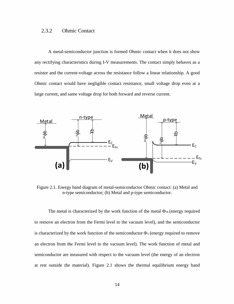
2.3.2 Ohmic Contact
A metal-semiconductor junction is formed Ohmic contact when it does not show
any rectifying characteristics during I-V measurements. The contact simply behaves as a
resistor and the current-voltage across the resistance follow a linear relationship. A good
Ohmic contact would have negligible contact resistance, small voltage drop even at a
large current, and same voltage drop for both forward and reverse current.
EC
EVqf
s
qχ
qf
m
Metaln-type
EC
EV
EFs
qf
s
qχ qf
m
Metalp-type
(a) (b)
EFs
Figure 2.1. Energy band diagram of metal-semiconductor Ohmic contact: (a) Metal and
n-type semiconductor; (b) Metal and p-type semiconductor.
The metal is characterized by the work function of the metal m (energy required
to remove an electron from the Fermi level to the vacuum level), and the semiconductor
is characterized by the work function of the semiconductor s (energy required to remove
an electron from the Fermi level to the vacuum level). The work function of metal and
semiconductor are measured with respect to the vacuum level (the energy of an electron
at rest outside the material). Figure 2.1 shows the thermal equilibrium energy band

15
diagram of a metal-semiconductor Ohmic contact for n-type and p-type semiconductor.
For Ohmic contact formation the metal work function should be less than the n-type
semiconductor work function and greater than the p-type semiconductor work function.
In both cases the Fermi levels are aligned between the metal and the semiconductor. The
difference between metal Fermi levels and semiconductor Fermi level diminishes at the
moment of forming the junction by exchanging charges at the edges of the bands. The
energy band diagrams shows that there is no barrier blocks to halt the flow of electrons in
the case of metal n-type contact and holes in the case of metal p-type contact. Hence the
current can flow through the junction regardless of the polarity of the applied voltage.
The 4H-SiC material used for Schottky diode fabrication can be considered as
intrinsic with the energy band-gap of ~3.26 eV at 300K [43] and the work function was
calculated to be 4.73 eV using Equation 2.1
𝜙𝑠 = 𝜒 +𝐸𝑔
2 2.1
where 𝜒 is the electron affinity (energy required to remove an electron from the
conduction band to the vacuum level), and 𝐸𝑔 is the band-gap. In order to form Ohmic
contact, deposited metal work function should be less than 4.73 eV.

16
2.3.3 Schottky Contact Formation and Energy Band Diagram
A metal-semiconductor contact is called Schottky contact when it has a rectifying
effect providing current conduction at forward bias (metal to semiconductor) and
presenting a low saturation current at reverse bias (semiconductor to metal). Figure 2.2
shows the Schottky metal-semiconductor contact after thermal equilibrium. In the
Schottky model, the vacuum level is assumed to be continuous across the interface and
the metal work function and semiconductor electron affinity are assumed to be constant
throughout the material right to the interface. In both cases it can be observed that the
Fermi levels are aligned between the metal and the semiconductor.
EFm EC
EV
qf
s
qχ
Metaln-type
EC
EV
EFs
qf
s
qχ
Metal
p-type
(a) (b)qf
m
qf
B
qV
0
qf
m
qV
0
EFs
W W
qf
B
Figure 2.2. Energy band diagram of metal-semiconductor Schottky contact; (a) Metal
and n-type semiconductor; (b) Metal and p-type semiconductor.
At the interface itself the vacuum level is same for the two sides such that there is
a barrier due to the difference between fm and . This difference, the ideal barrier of the
junction, fB, is given by the following equation 2.2

17
𝑞ɸ𝐵 = 𝑞(ɸ𝑚 − 𝜒) 2.2
The rectifying effect of the Schottky contact is due to the formation of this barrier
height (qfB) at the junction. So it is important to note that the condition to form a
Schottky barrier for a n-type semiconductor is is fm > fs and for p-type semiconductor is
fm < fs For n-type semiconductor as the distance from the interface increases, the
conduction band bends to match with the bulk region value. This band bending builds an
electric field which sweeps free electrons from the vicinity of the contact interface and
creates fixed positive charge distribution due to ionized donors and thus forms a
depletion region (also known as space charge region). The bands become flat at the edge
of depletion region and the electric field falls to zero at the edge which persists
throughout the semiconductor. In the metal side a neutralizing negative charge is
accumulated at the contact. A Schottky junction is consists of a space charge region
(entirely depleted of mobile charge) and an electrically neutral bulk region where they are
separated by a sharp interface [44].
Electrons coming from the n-type semiconductor into the metal face a barrier
known as built-in voltage (Vbi) are obtained from fm-fs. The barrier faced by holes
moving from p-type semiconductor to metal is fs-fm. The depletion width for a Schottky
barrier on an n-type semiconductor can be obtained following expression [45],

18
𝑊 = √2×𝑉𝑏𝑖×𝜀×𝜀0
𝑞×𝑁𝐷 2.3
where 𝜀 𝑖𝑠 the dielectric constant of the semiconductor material, 𝜀0 is the
permittivity of vacuum, 𝑞 is the electronic charge (1.6 × 10⁻¹⁹
C) and 𝑁𝐷 is the effective
doping concentration and Vbi is the built-in potential. For n-type semiconductor the built-
in voltage Vbi is given by
𝑉𝑏𝑖 = ɸ𝐵 −𝑘𝑇
𝑞ln (
𝑁𝐶
𝑁𝐷) 2.4
A forward bias opposes the built-in voltage and reduces the overall band bending
while a reverse bias does the opposite.
2.3.4 Carrier Transport Mechanism
The current transport in metal-semiconductor contacts is mainly due to majority
carriers. The various electrons transport mechanisms across a metal – semiconductor
junction under a forward bias are as follows [46]:
a. Electron thermionic emission over the top of the barrier (holes for p-type
material) in which electrons with energies greater than the barrier height can
pass across the junction
b. Quantum mechanical tunneling which is important for heavily doped
semiconductors where the depletion width is small.
c. Depletion width is small. Recombination in the space charge region

19
d. Recombination in the neutral region.
Figure 2.3. Transport process in a forward biased Schottky barrier
The four different electron transport mechanisms are shown in Figure 2.3. Besides
this, edge leakage current may flow at the contact periphery due to high electric field.
There may also be current flow due to traps at the metal-semiconductor interface. The
inverse process happens under the reverse bias. In ideal cases, the current flows mainly
by the process (a). The other processes (b), (c), and (d) are responsible for the departures
from ideality. The electron emission over the barrier from semiconductor to metal is

20
governed by two basic processes: (i) electrons transport from the bulk semiconductor and
across the depletion region by diffusion and drift in the barrier electric field and (ii) the
electron emission at metal-semiconductor interface which is determined by the rate of
transfer of electrons across the boundary. According to the diffusion theory of Schottky
[47], the first process is dominant one. According to Bethe thermionic–emission theory
[48], the second process, the actual transfer of electrons across the metal-semiconductor
interface, is a current limiting factor.
2.3.5 Current-Voltage (I-V) Analysis
Many semiconductor devices; such as p-n and Schottky junctions, solar cells,
photodiodes, MOSFET etc., electrical performances are evaluated through current-
voltage (I-V) characteristics. The performance level and degradation are highly
dependent upon the material, the operating current flowing through the device and series
resistances. The voltage dependent junction current in a Schottky contact can be
expressed as [46]:
𝐼 = 𝐼𝑠(𝑒𝛽𝑉
𝑛 − 1) 2.5
where 𝐼𝑆 is the saturation current, V is the applied voltage, 𝑛 is the diode ideality
factor, 𝛽 = 𝑞/𝑘𝐵𝑇, 𝑞 being the electronic charge (1.6 × 10⁻¹⁹
C), 𝑘𝐵 the Boltzmann
constant (8.62 × 10⁻⁵
eV/K), and 𝑇 is the absolute temperature (°K). The saturation
current is given by Equation 2.6

21
𝐼𝑆 = 𝐴∗𝐴𝑇2(𝑒−𝛽𝜑𝐵) 2.6
where 𝐴 is the area of the diode, 𝜑𝐵 is the Schottky barrier height, and 𝐴∗ is the
effective Richardson constant which can be expressed as [49]
𝐴∗ = 4𝜋2 𝑚∗ ℎ3⁄ = 120 (𝑚∗ 𝑚) 𝐴𝑐𝑚−2⁄ 𝐾−2 2.7
where h is Planck constant, and m* is the electron effective mass .
Plot of log (I) vs. V will be a straight line if I0 and n are constant. The voltage
across the diode becomes Vd = V - IRs, where Rs is the series resistance of the diode and
V is the measured voltage across the entire diode including contact resistance as well as
other resistance components.
𝐼 = 𝐼𝑠(𝑒𝛽(𝑉−𝐼𝑅𝑠)
𝑛 − 1) 2.8
By taking the logarithm the equation 2.6 can be written as
log(𝐼) =𝛽𝑉
𝑛+ log(𝐼𝑆) 2.9
which is an equation of straight line where 𝛽
𝑛 is the slope and log(𝐼𝑆) is the
intercept as shown in Figure 2.4. The plot gives a straight line over the range where the
condition IRs<<V and kBT/q<<1 are satisfied. The plot deviates from straight line for
lower current due to the term -1 in the parenthesis of the equation and deviates from

22
straight line for higher current due to series resistance. The slope and the intercept can be
easily calculated using a linear regression of log (I) vs V plot obtained from I-V
measurements. As the sample temperature is known, the ideality factor is obtained from
the measured slope according to the equation 2.10.
𝑛 = 1
𝑠𝑙𝑜𝑝𝑒 ×1𝛽⁄
2.10
.
Figure 2.4. Linear fit of current-voltage (I-V) acquired data plotted in logarithmic scale
The reverse saturation current Is is obtained by extrapolation of the straight line
portion of the curve, and surface barrier height is calculated from the equation. The diode
ideality factor gives the uniformity of surface barrier height across the detector surface
[50]. An ideality factor greater than unity, indicates the presence of patches (i.e. presence
of generation-recombination centers) on the detector surface where the surface barrier
height is considerably lower than the rest of the surface [51].

23
2.3.6 Capacitance-Voltage (C-V) Analysis
The voltage dependence of the capacitance (C-V) measurement relies on the fact
that the depletion region width of a semiconductor junction depends upon the applied
voltage. The effective doping concentration (ND) in the active region of a Schottky diode
or p-n junction can be obtained from the C-V measurement. The knowledge of effective
doping concentration allows the calculation of the depletion width under certain applied
bias (According to Equation 2.11) and also the determination of full depletion bias. In
order to calculate the doping concentration and the built-in voltage, analysis of the data
acquired from capacitance-voltage (C-V) measurements is needed.
Figure 2.5. Capacitance-voltage data acquired using a Schottky diode.
Figure 2.5 shows a C-V measurement conducted on a Schottky device. The
capacitance can be seen decreasing with the increase in reverse bias because the
capacitance is inversely proportional to the depletion width as is shown in Equation 2.11
and the depletion width in a p-n junction or Schottky diode increases as reverse bias
increases. Mathematically, the capacitance of a Schottky diode can be expressed as [52],

24
𝐶 =𝜀 × 𝜀0 × 𝐴
𝑊= 𝐴 [
𝜀𝜀0𝑁𝐷
2(𝑉𝑏𝑖 + 𝑉)]
1 2⁄
2.11
where the symbols have their usual meaning.
The variation in capacitance as a function of reverse bias is given by
1
𝐶2=
2𝑉𝑏𝑖
𝐴2𝑞𝜀𝜀0𝑁𝐷+
2𝑉
𝐴2𝑞𝜀𝜀0𝑁𝐷 2.12
which is a straight line equation in a 1/C2 vs. V plot. The doping concentration 𝑁𝐷
is calculated by the following equation:
𝑁𝐷 =2
𝐴2𝑞𝜀𝜀0 × 𝑠𝑙𝑜𝑝𝑒
2.13
The first term of Equation 2.12 allows calculation of the built-in voltage (Vbi)
using the intercept obtained from the linear fit. Figure 2.6 shows one such linear 1/C2 vs.
V plot obtained for a Schottky diode.

25
Figure 2.6. 1/C2 vs. reverse bias plot with linear fitting. Variation of 1/C
2 as a function of
reverse bias corresponding to the C-V plot shown in above . The straight line shows the
linear fit of the experimental data.
2.4 CONCLUSION
In this chapter material properties and the crystal structure of SiC are discussed.
The crystal growth process for both bulk and epitaxial layer are also described briefly.
The theoretical concepts of the device’s structure used in the experiments of this thesis
are explained here. For the detector fabrication, it is important to understand how to
obtain the desired type of metal-semiconductor contact, e.g. Ohmic or Schottky. For
Schottky contacts, the thermionic emission model is described in order to study the
contacts’ properties in SiC diodes in terms of the barrier height and the ideality factor
using current-voltage (I-V) measurements. For further characterization of the Schottky
contact, the calculation procedures for doping concentration and built-in voltage using
capacitance-voltage (C-V) measurements are described.

26
CHAPTER 3: DEFECTS IN SIC
3.1 OVERVIEW
Defects in semiconductors can be classified as: point defects and extended
defects. Point defects are localized in a lattice site, involving only a few nearest neighbors
and not extended to any spatial dimensions. Extended defects, such as, grain boundaries,
dislocations and/or stacking faults, are extended in all dimensions and will be discussed
in the next section. This chapter will discuss on the defects and their detrimental
properties.
3.2 POINT DEFECTS
Point defects exist in small concentrations in all semiconductor materials and
formed mainly due to vacancies, interstitials, and substitutions. Aggregation of few point
defects which generate a perturbation in a lattice site and its immediate vicinity, such as,
divacancies, vacancy–donor complexes, are also considered as point defects. Point
defects introduce electronic energy states within the semiconductor band-gap which can
act as, ‘traps’, ‘recombination centers’, or ‘generation centers’ and may modify the
semiconductor properties and device performances significantly. The point defects are
27
desirable for some devices and introduced intentionally. As for example, in switching
devices, energy levels introduced by point defects can be used as recombination centers
which help to remove minority carriers quickly during turning off and enhance the
device’s switching speed thereby increasing efficiency [53, 54]. However for many cases
point defects are detrimental to the device performances. Energy states created by point
defects may act as a recombination centers for the generated electron-hole pairs and
degrade the performance of radiation detectors and photovoltaic solar cells. Point defects
and their characterization will be discussed in detail in chapter five of this dissertation.
3.3 MORPHOLOGICAL DEFECTS
Most SiC devices are fabricated is such a way that their electrically active regions
resides entirely within the epilayer grown on bulk crystal substrate. The electrical
characteristics of these devices critically depend on the quality and smoothness of the
semiconductor surface. So the defects contained in the epilayer are of great interest to any
opto-electrical devices. The defects in SiC epilayer that impact electrical device
performances are threading screw dislocation (TSD), threading edge dislocation (TED),
basal plane dislocation (BPD), small growth pits, triangular inclusions, carrots, and comet
tail defects [55, 56, 57]. Lot of defects originated in bulk cannot propagate to the
epilayer, so the epitaxial layer contains significantly fewer defects than bulk wafers.

28
3.3.1 Threading Screw Dislocation (TSD) and Micropipes
Threading screw dislocation (TSD) can penetrate along the crystallographic c-axis
through the entire length of the crystal. Screw dislocations terminate only in the crystal
surface and are present in all wafers cut from the grown crystal. This screw dislocation
can propagate throughout the whole thickness of epitaxial layer grown by CVD
technique. Additional screw dislocation may also form during the epitaxial growth [58,
59]. Extended screw dislocation is usually measured by the length of the Burgers vector
(b). For pure screw dislocation the Burgers vector is parallel to the crystallographic c-axis
and the Burger vector length is related to the step height of the screw dislocation.
Screw dislocation with large Burger vector forms hollow cores and is widely
known as micropipes. Micropipes are hollow tubular defects penetrating the SiC single
crystals and their radius ranges from a few tens of nanometers to several tens of
micrometers. The performance of SiC based power devices and radiation detectors is
severely degraded by these micropipes [56, 60, 61]. Substrate micropipe defects with an
area of 1 mm2 or larger may cause pre-avalanche reverse-bias point failure in epitaxially
grown p-n junction devices. With the steady development of the material growth process,
the micorpipe densities have been reduced drastically (from 104 cm
-2 to less than 1 cm
-2)
and recently vendors have grown micropipe-free epitaxial layers [57].
The SiC screw dislocation with small Burgers vector forms close core and
sometimes termed as elementary screw dislocations which exist at densities on the order

29
of thousands per cm2 in 4H- and 6H-SiC wafers and epilayers [62]. Close core
dislocation is not as detrimental as micropipes, however, experimentally it is proven that
theses defects have negative impact on device performances [63]. It is found that soft
breakdown (at voltage <250 V) in 4H-SiC p-n junction diodes may happen due to these
close core dislocation [64]. Wahab et al. showed that increasing density of close core
dislocations in the active region can cause the degradation of the breakdown voltages
[65].
3.3.2 Basal Plane Dislocation (BPD)
Basal plane dislocations (BPDs) probably have the highest density of all the
dislocations. BPDs form to relaxation of the thermal stress which mainly occurred during
cooling down from high growth temperature to room temperature. BPDs in p-n diodes
may dissociate into two Shockley partials and cause an increase of forward voltage drop
[66]. Basal plane tilt low angle grain boundaries due to the pile-up of BPDs [67].
3.3.3 Threading Edge Dislocation (TED)
Threading edge dislocation (TED) is an edge type dislocation which has Burgers
vectors perpendicular to along the c-axis of the crystal. TEDs are mostly inherited from
the substrate. Basal plane dislocations (BPDs) propagate from the off-axis 4H-SiC
substrate into the homoepitaxial layer and convert into threading edge dislocations in the
epitaxial layer. The conversion from BPDs to TEDs happens due to the image force in the

30
epilayers. The converted dislocations are inclined from the c-axis toward the down-step
direction by about 15ο [68]. Ha et al. [69] suggest that TEDs may also form due to
prismatic plane slip.
3.3.4 Staking Faults
Staking faults (SFs) are kind of planar defects and exist mostly in the primary slip
plane {0001} of SiC. SFs occur due to the deviation of Si–C bilayers from the perfect
stacking sequence along the c-axis of the crystal. SFs reduce the barrier height and the
breakdown voltage of a Schottky diode. An electrostatic potential may appear in SiC p-i-
n diodes due to the charge accumulation in the stacking faults and can increase the
forward voltage drop in the diode [68].
3.4 MORPHOLOGICAL DEFECTS DELINEATION BY ETCHING
Chemical etching of silicon carbide is the most versatile way to characterize
silicon carbide crystals and has been used effectively to evaluate the crystal qualities.
Most of the chemicals used in chemical etching process are used in molten state. Since
the sublimation temperature of SiC is 2830 ˚C, it is possible to etch SiC at temperature as
high as 1200 ˚C. Due to high amount of hazards involved in etching SiC at such high
temperature, a new method of etching SiC at low temperature is absolutely necessary.
Molten KOH etching is the widely used method of etching to investigate the growth
defects in SiC wafers. SiC etching by molten KOH is an isotropic etching which is a non-

31
directional etching with uniform etch rate in all directions of the wafers. So molten KOH
remove the SiC surface layers at the same etch rate in all directions irrespective of the
crystal orientation.
3.4.1 Experimental Procedure for SiC Etching
In our studies, etching studies have been conducted for bulk 4H-SiC crystals and
4H-SiC epitaxial layers. The epilayers were grown by chemical vapor deposition on ~
350 m 4H-SiC thick substrate. Both the bulk and the epitaxial layers were diced into
10×10 mm2 size. Before etching, the samples have been cleaned thoroughly by an
established procedure. This involved cleaning tri-chloro-ethylene (TCE) for 5 minutes
and cleaning in HF and acetone for 5 min successively. A nickel crucible, inert to molten
KOH, was used for holding the dry KOH pellets. A hot plate was used for heating the
nickel crucible containing the KOH pellets. The temperature of the crucible is monitored
by a thermocouple and the temperature was controlled with the help of a knob of the hot
plate. The temperature is gradually increased to 500 ˚C to melt the KOH pellets. The SiC
samples were immersed into the molten KOH with the help of a specially designed
sample holder. The sample holder is also made from a thick nickel sheet. Throughout the
etching period, KOH solution temperature is kept constant (~ 500 ˚C) by adjusting the
power knob of the hot plate. After 20 minutes of etching, the samples were taken out
from the solution and quickly washed by acidified water to neutralize the KOH. After
repeated cleaning by DI water, the samples were finally cleaned with acetone. The whole
etching experiment was carried out inside the chemical hood in the advanced

32
microelectronic materials laboratory at USC. A very thin layer (~ 5 nm) of gold was
deposited on the etched surface of SiC samples for SEM studies.
3.4.2 Result of SEM Studies
Figure 3.1 shows the SEM image of a Si-face etched bulk SiC crystal. In the SEM
images observed pits with hexagonal shapes are correlated to three types of dislocations.
Hexagonal pits with a small black spot in the center are the closed-core screw
dislocations [70, 71, 72]. The larger hexagonal pits with a hollow core in the center are
considered as the open-core screw dislocations (micropipes) [73, 74]. Hexagonal pits
without any center spot are the treading edge dislocations [72, 73]. The hexagonal pits
images corresponding to the treading edge dislocations are less bright than those of open
core or close core dislocations. In the SEM image shown in Figure 3.1 (b), the basal
plane dislocations are appeared as sharp elongated lines which are formed by the
interconnection of a series of asymmetrical pits. Figure 3.2 shows the magnified images
of the following observed dislocations.
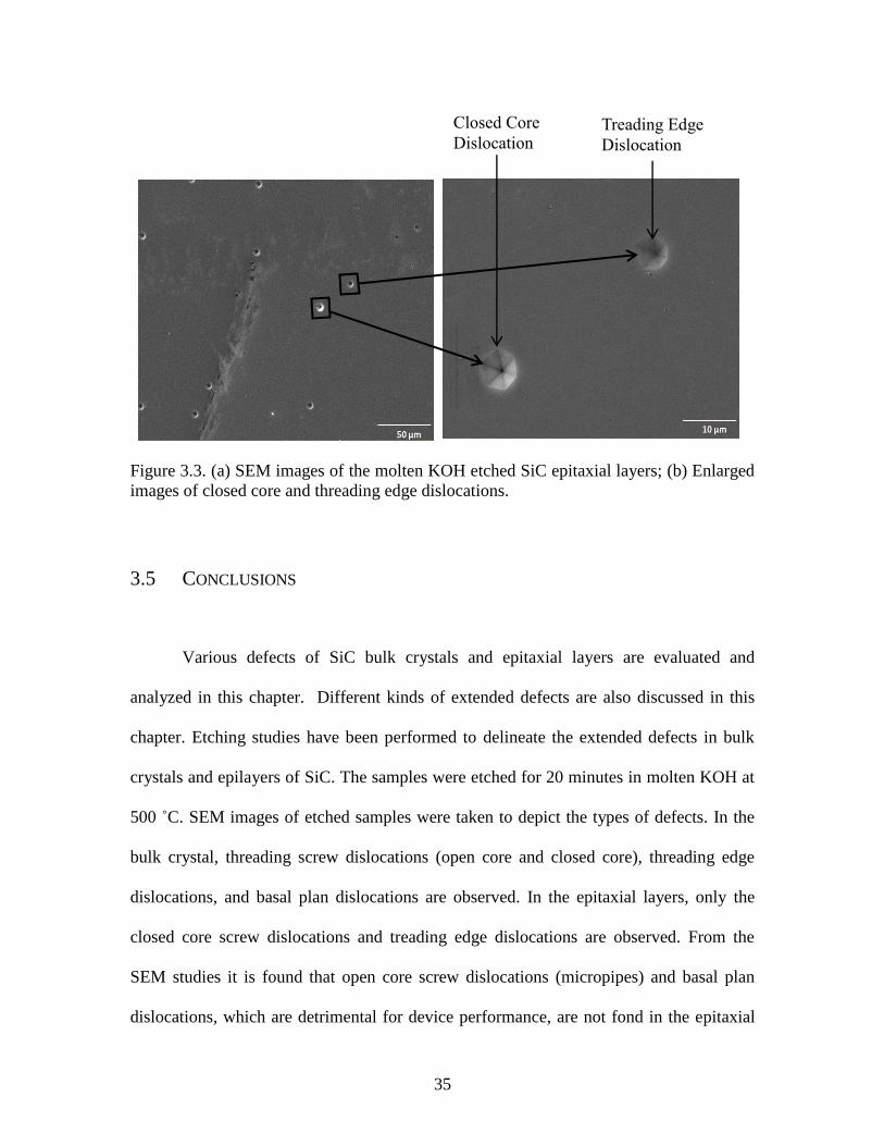
Figure 3.3 (a) shows the SEM images of etched SiC epitaxial layers. The
experimental set up and etching process was kept exactly the same for both bulk and
epitaxial layers. Figure 3.3 (b) shows the enlarged SEM images of closed core
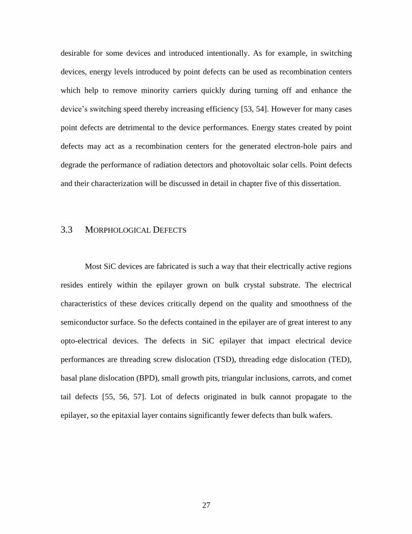
dislocations and threading edge dislocations of the epitaxial layers. The densities of the
identified dislocations are much lower in the epitaxial layer compared to the bulk

33
crystals. Micropipes and BPDs are not observed in the SEM images of the etched
epitaxial layers.
Figure 3.1. SEM image of the molten KOH etched bulk SiC: (a) Region with TSDs and
TEDs; (b) Regions with BPDs and TEDs.
Closed Core Screw
Dislocation
Threading Edge
Dislocation
Basal Plane
Dislocation
Micropipes
(a)
(b)

34
Figure 3.2. SEM images of the molten KOH etched bulk SiC: (a) Region with TSDs and
TEDs; (b) Enlarge images of micropipes; (C) ) Enlarge images of closed core and
threading edge dislocations.
Open Core Screw Dislocations
(Micropipes)
Closed Core Screw Dislocations
Threading Edge Dislocations
(a) (b)
(c)
35
Figure 3.3. (a) SEM images of the molten KOH etched SiC epitaxial layers; (b) Enlarged
images of closed core and threading edge dislocations.
3.5 CONCLUSIONS
Various defects of SiC bulk crystals and epitaxial layers are evaluated and
analyzed in this chapter. Different kinds of extended defects are also discussed in this
chapter. Etching studies have been performed to delineate the extended defects in bulk
crystals and epilayers of SiC. The samples were etched for 20 minutes in molten KOH at
500 ˚C. SEM images of etched samples were taken to depict the types of defects. In the
bulk crystal, threading screw dislocations (open core and closed core), threading edge
dislocations, and basal plan dislocations are observed. In the epitaxial layers, only the
closed core screw dislocations and treading edge dislocations are observed. From the
SEM studies it is found that open core screw dislocations (micropipes) and basal plan
dislocations, which are detrimental for device performance, are not fond in the epitaxial
Treading Edge
Dislocation
Closed Core
Dislocation

36
layers. Moreover the densities of the delineated defects in the 4H-SiC epitaxial layers are
much less compared to the bulk crystals. So it is clear that substantial amount of bulk
crystal defects are not being propagated to the epitaxial layers during the epitaxial
growth.
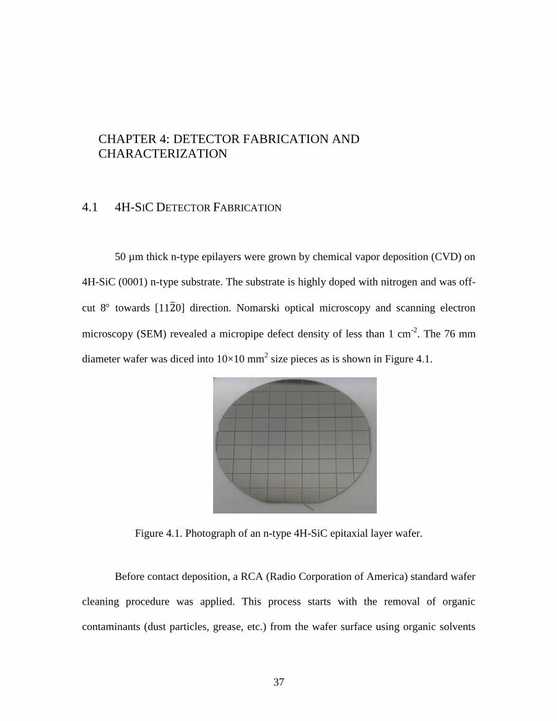
37
CHAPTER 4: DETECTOR FABRICATION AND
CHARACTERIZATION
4.1 4H-SIC DETECTOR FABRICATION
50 µm thick n-type epilayers were grown by chemical vapor deposition (CVD) on
4H-SiC (0001) n-type substrate. The substrate is highly doped with nitrogen and was off-
cut 8 towards [112̅0] direction. Nomarski optical microscopy and scanning electron
microscopy (SEM) revealed a micropipe defect density of less than 1 cm-2
. The 76 mm
diameter wafer was diced into 10×10 mm2 size pieces as is shown in Figure 4.1.
Figure 4.1. Photograph of an n-type 4H-SiC epitaxial layer wafer.
Before contact deposition, a RCA (Radio Corporation of America) standard wafer
cleaning procedure was applied. This process starts with the removal of organic
contaminants (dust particles, grease, etc.) from the wafer surface using organic solvents

38
(trichloroethylene, acetone, and methanol) at their respective boiling temperatures. Any
organic residue left by the first step is then processed using sulfuric acid (H2SO4) and
ammonium hydroxide (NH4OH) solutions (with hydrogen peroxide). These solutions are
designed to attack the organic impurities by dehydration and oxidation of the carbon
present forming oxide at the surface of the wafer. Finally, these oxide layers were etched
with hydrofluoric acid (HF).
The Schottky barriers were formed on the epitaxial layers (Si face) by depositing
thin (10 nm) circular Ni contacts (area ~11.95 mm2). 100 nm thick square (~ 64 mm
2) Ni
back contacts were deposited on the C face of the 4H-SiC substrates. A Quorum model Q
150T DC sputtering unit was used to deposit the metal contacts. The cross-sectional
schematic of the fabricated Schottky barrier radiation detector is shown in Figure 4.2.
Figure 4.2. Schematic diagram of the cross-sectional view of 50µm thick n-type 4H-SiC
Schottky barrier device.

39
4.2 ELECTRICAL CHARACTERISTICS OF FABRICATED DETECTOR
Current-voltage (I-V) and capacitance-voltage (C-V) measurements were
conducted in order to investigate the electrical properties of the metal-semiconductor
contact. The I-V measurements were carried out using a Keithley 237 high voltage
source-measure unit. Forward and reverse I-V characteristics were acquired to study the
behavior of the Schottky contact. C-V measurements were carried out at 100 kHz using a
Keithley 590 C-V meter. Figure 4.3 shows the schematic and the arrangement of the
equipment setup used to perform the I-V and C-V measurements.
Figure 4.3. Schematic of the I-V and C-V experimental setup.

40
The picture of the I-V and C-V measurement system at USC is shown in Figure
4.4. To minimize the influence of external electrical and optical signal, the detector is
mounted in an EMI shielded aluminum box during the measurement.
Figure 4.4. Photograph of the experimental setup for the I-V and C-V measurements. The
detector is mounted inside the aluminum box.
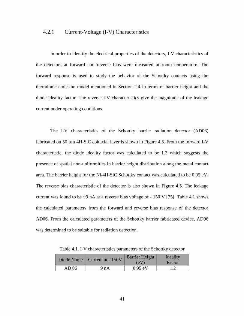
41
4.2.1 Current-Voltage (I-V) Characteristics
In order to identify the electrical properties of the detectors, I-V characteristics of
the detectors at forward and reverse bias were measured at room temperature. The
forward response is used to study the behavior of the Schottky contacts using the
thermionic emission model mentioned in Section 2.4 in terms of barrier height and the
diode ideality factor. The reverse I-V characteristics give the magnitude of the leakage
current under operating conditions.
The I-V characteristics of the Schottky barrier radiation detector (AD06)
fabricated on 50 µm 4H-SiC epitaxial layer is shown in Figure 4.5. From the forward I-V
characteristic, the diode ideality factor was calculated to be 1.2 which suggests the
presence of spatial non-uniformities in barrier height distribution along the metal contact
area. The barrier height for the Ni/4H-SiC Schottky contact was calculated to be 0.95 eV.
The reverse bias characteristic of the detector is also shown in Figure 4.5. The leakage
current was found to be ~9 nA at a reverse bias voltage of - 150 V [75]. Table 4.1 shows
the calculated parameters from the forward and reverse bias response of the detector
AD06. From the calculated parameters of the Schottky barrier fabricated device, AD06
was determined to be suitable for radiation detection.
Table 4.1. I-V characteristics parameters of the Schottky detector
Diode Name Current at - 150V Barrier Height
(eV)
Ideality
Factor
AD 06 9 nA 0.95 eV 1.2
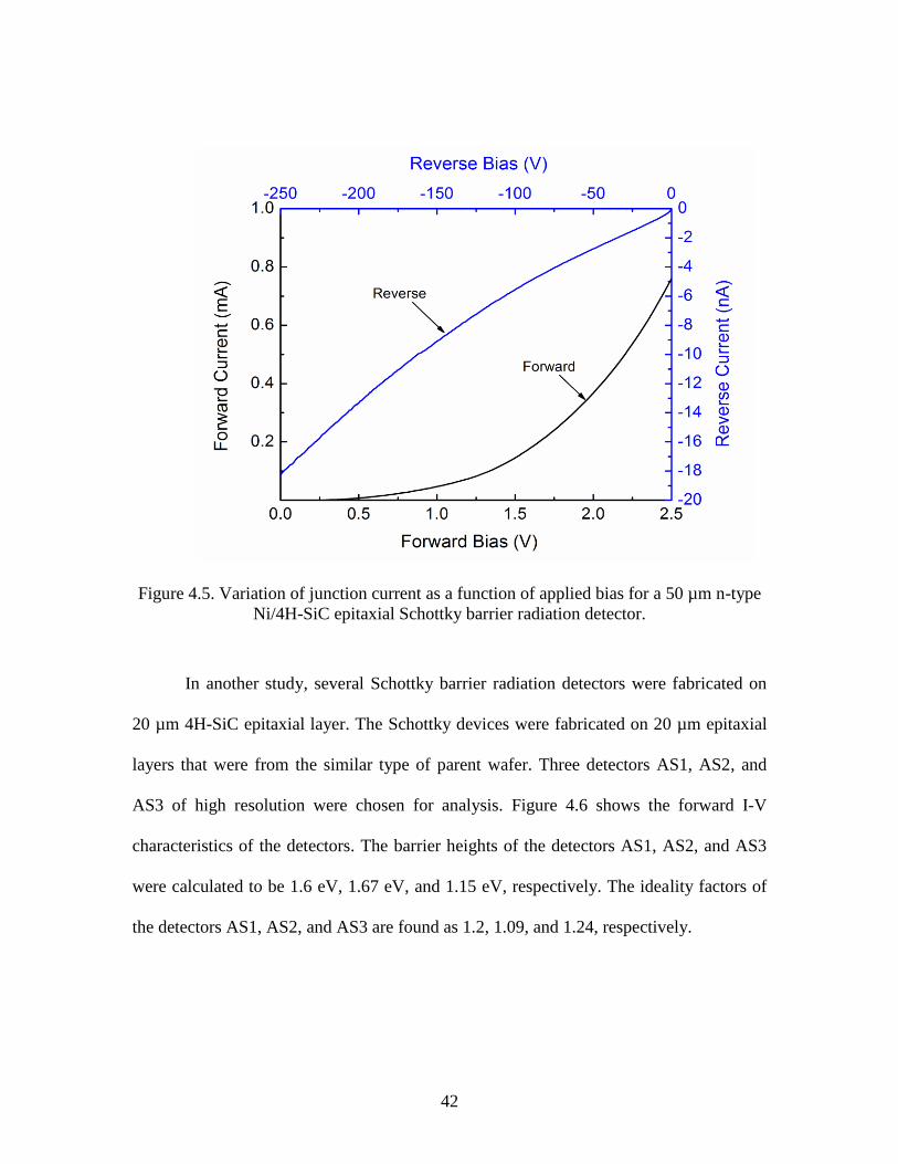
42
Figure 4.5. Variation of junction current as a function of applied bias for a 50 µm n-type
Ni/4H-SiC epitaxial Schottky barrier radiation detector.
In another study, several Schottky barrier radiation detectors were fabricated on
20 µm 4H-SiC epitaxial layer. The Schottky devices were fabricated on 20 µm epitaxial
layers that were from the similar type of parent wafer. Three detectors AS1, AS2, and
AS3 of high resolution were chosen for analysis. Figure 4.6 shows the forward I-V
characteristics of the detectors. The barrier heights of the detectors AS1, AS2, and AS3
were calculated to be 1.6 eV, 1.67 eV, and 1.15 eV, respectively. The ideality factors of
the detectors AS1, AS2, and AS3 are found as 1.2, 1.09, and 1.24, respectively.

43
Figure 4.6. Forward I-V characteristics on 4H-SiC epitaxial Schottky barrier detectors
AS1, AS2, and AS3.
Figure 4.7 shows the reverse I-V characteristics of the three detectors. The
leakage currents at -110 V for AS1, AS2, and AS3 were 4.3 pA, 6.2 pA, and 10.0 pA,
respectively. Detector AS1 exhibited the lowest leakage current among these three
detectors at the operating voltage (~110 V) of the detectors.

44
Figure 4.7. Reverse I-V characteristics obtained for 4H-SiC epitaxial Schottky barrier
detectors AS1, AS2, and AS3.
4.2.2 Capacitance-Voltage (C-V) Characteristics
Figure 4.8 shows a 1/C2 vs V plot, and the inset shows the original C-V plot. In a
Schottky metal-semiconductor junction, the depletion region extends to the side of the
semiconductor and increases its width with the increase in reverse bias; this property
allows control of the depletion width in the epitaxial layer which defines the active
region. The active region is where the charge signal due to particle interaction takes place
(creation of electron-hole pairs) in the detector. As the capacitance value depends on the
contact area and width of the depletion region, as shown in Section 2.4, capacitance is

45
expected to decrease as reverse bias increases. Further analysis of the acquired data was
performed in order to calculate the doping concentration of the epilayer and the built-in
voltage of the Schottky contact. As expected, the capacitance values showed a decreasing
trend with the increasing reverse bias because of the increase in depletion width. The
effective doping concentration (Neff) was calculated to be 1.98×1015 cm-3
and the built-in
potential (Vbi) of the contact was found to be 1.5 V from 1/C2 vs V plots.
Figure 4.8. 1/C2 vs V plot for a 50 µm n-type Ni/4H-SiC epitaxial Schottky barrier
detector. The open circles are the experimental data points and the solid line is a straight
line fit to the experimental data. Inset shows the original C-V plot.
The Schottky barrier height was also calculated from the C-V characteristics.
Considering the standard band diagram for an abrupt p-n junction, the barrier height can
be expressed as

46
∅𝐵(𝐶−𝑉) = 𝑉𝑏𝑖 + 𝑉𝑛 4.1
where, Vn is the energy difference between the Fermi level and the conduction
band minimum and can be expressed as
𝑉𝑛 = 𝑘𝑇𝑙𝑛𝑁𝐶
𝑁𝑒𝑓𝑓 4.2
where NC is the effective density of states in the conduction band of 4H-SiC and
is taken equal to 1.7×10¹⁹
cm-3
[76]. The barrier height thus calculated from C-V
measurements was 1.7 eV which is higher than that obtained from the forward I-V
characteristics. The difference between the two barrier height values can be explained as
follows. Barrier height obtained from the forward I-V characteristics is generally
dominated by current flow through the low Schottky barrier height locations over the
entire metal contact area in an inhomogeneous Schottky diode which results in lower
surface barrier height. C-V characteristics, on the other hand, give an average value of the
barrier height for the whole diode area [50, 77]. The larger value of barrier height
calculated from the C-V measurements reconfirms the spatial inhomogeneity of the
surface barrier height as was also inferred from the ideality factor value.
Figure 4.9 shows the 1/C2 vs V plots for the three detectors ( AS1, AS2, and
AS3).The calculated effective doping concentrations for the detectors are the following:
AS1 is 2.6 × 10¹⁴
cm-3
, AS2 is 3.2 × 10¹⁴
cm-3
, and AS3 is 2.6 × 10¹⁴
cm-3
. The effective
doping concentration was found to be the least for the detector AS1 among all the three
detectors.

47
Figure 4.9. 1/C2 vs V plots for 4H-SiC epitaxial Schottky barrier radiation detectors AS1,
AS2, and AS3.
4.3 RADIATION INTERACTION WITH SEMICONDUCTOR MATERIALS
Alpha particles continuously interact with the semiconductor material as they pass
through by the Coulomb force with electrons in the material. If the transferred kinetic
energy exceeds the electron’s binding energy, ionization occurs which gives rise to the
creation of an electron-hole pair. If a charged particle of mass m with kinetic energy E
interacts with an electron of mass m0, the maximum transferable energy is 4Em0/m in a
single collision. Continuous interactions with various electrons in the absorber material
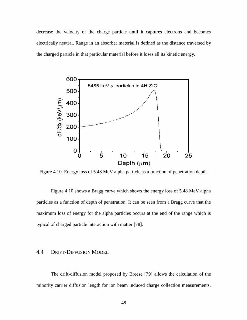
48
decrease the velocity of the charge particle until it captures electrons and becomes
electrically neutral. Range in an absorber material is defined as the distance traversed by
the charged particle in that particular material before it loses all its kinetic energy.
Figure 4.10. Energy loss of 5.48 MeV alpha particle as a function of penetration depth.
Figure 4.10 shows a Bragg curve which shows the energy loss of 5.48 MeV alpha
particles as a function of depth of penetration. It can be seen from a Bragg curve that the
maximum loss of energy for the alpha particles occurs at the end of the range which is
typical of charged particle interaction with matter [78].
4.4 DRIFT-DIFFUSION MODEL
The drift-diffusion model proposed by Breese [79] allows the calculation of the
minority carrier diffusion length for ion beam induced charge collection measurements.

49
For radiation detection applications, this model is used to calculate the separate
contribution of charge carriers produced in the depletion region and that of the diffusion
of holes created in the neutral region to the experimentally determined overall charge
collection efficiency (CCEobs). Equation 4.3 describes the concept applied to the model.
𝐶𝐶𝐸𝑡ℎ𝑒𝑜𝑟𝑦 =1
𝐸𝑝∫ (
𝑑𝐸
𝑑𝑥)
𝑑
0
𝑑𝑥 +1
𝐸𝑝∫ [(
𝑑𝐸
𝑑𝑥) × exp {−
𝑥 − 𝑑
𝐿𝑑}] 𝑑𝑥
𝑥𝑟
𝑑
= 𝐶𝐶𝐸𝑑𝑟𝑖𝑓𝑡 + 𝐶𝐶𝐸𝑑𝑖𝑓𝑓𝑢𝑠𝑖𝑜𝑛
4.3
where 𝐸𝑝 is the energy of the alpha particles, 𝑑 is the depletion width at the
particular bias, 𝑑𝐸
𝑑𝑥 is the electronic stopping power of the alpha particles calculated using
SRIM 2012 [80], 𝑥𝑟 is the projected range of the alpha particles with energy 𝐸𝑝, and 𝐿𝑑 is
the diffusion length of the minority carriers. The first term of the Equation 4.10,
𝐶𝐶𝐸𝑑𝑟𝑖𝑓𝑡, gives the contribution of charge generated within the depletion region to the
charge collection efficiency and the second term, 𝐶𝐶𝐸𝑑𝑖𝑓𝑓𝑢𝑠𝑖𝑜𝑛, is that from the charge
carriers created in the region behind the depletion region and diffused to the depletion
region.
4.5 RADIATION DETECTION
4.5.1 Pulse-height Spectrum
Once an alpha particle has deposited its energy into a detector which generates
electron-hole pairs, the signal is extracted by the front-end electronics. Figure 4.11 shows

50
a typical radiation detection measurement setup which will process the signals produced
by the detector into a useable form. The charge signal seen by the detector requires
immediate amplification to prevent signal loss, due to the small amounts of charge
involved. A preamplifier performs this initial amplification, which will allow the charge
signal to be converted to a voltage signal, which can be sent over standard BNC cables to
a shaping amplifier.
Figure 4.11. Schematic diagram of an analog radiation detection measurement system.
Preamplification is a critical step for signal processing in the detection system
because noise introduced in this stage of the detection setup can have a significant effect
on the resulting pulse-height spectrum. Figure 4.12 shows a basic charge-sensitive
preamplifier circuit, and the effect the preamplifier has on the signal coming from the
detector. A charge-sensitive preamplifier at its basic level consists of a high gain
amplifier with a feedback capacitor and feedback resistor. The feedback capacitor makes
the preamplifier insensitive to changes in the capacitance of the detector, while adding
some noise to the circuit. Furthermore, a FET is usually used at the input of the high-gain
amplifier, which must be carefully selected for noise consideration purposes.
e
h
Nuclear
radiation
Pre-
AmplifierShaping
AmplifierMCA
Detector High Voltage
Supply Oscilloscope
e
h
Nuclear
radiation
Pre-
AmplifierShaping
AmplifierMCA
Detector High Voltage
Supply Oscilloscope

51
Figure 4.12. (a) Simplified circuit diagram for a charge sensitive preamplifier used in a
detection system. (b) Input and output pulse shapes seen by a preamplifier [7]
After preamplification, the signal is sent to a shaping amplifier. The preamplifier
pulse output contains background noise generated by both the preamplifier circuit and the
detector itself. For this reason, these pulses are shaped by a shaping amplifier, which will
filter as much noise as possible while preserving information about the energy of the
radiation seen by the detector. This is done by passing the preamplifier signal through
one stage of differentiation (using a CR, or high pass circuit) and several stages of
integration (using an RC, or low pass circuit). Figure 4.13 shows the effect of a shaping
amplifier on a preamplifier output signal as well as the analog circuitry and stages of CR
and RC shaping used in a shaping amplifier. The shaping amplifier will spend a certain
amount of time, τm, measuring the signal, which is also known as the shaping time.
(a) (b)
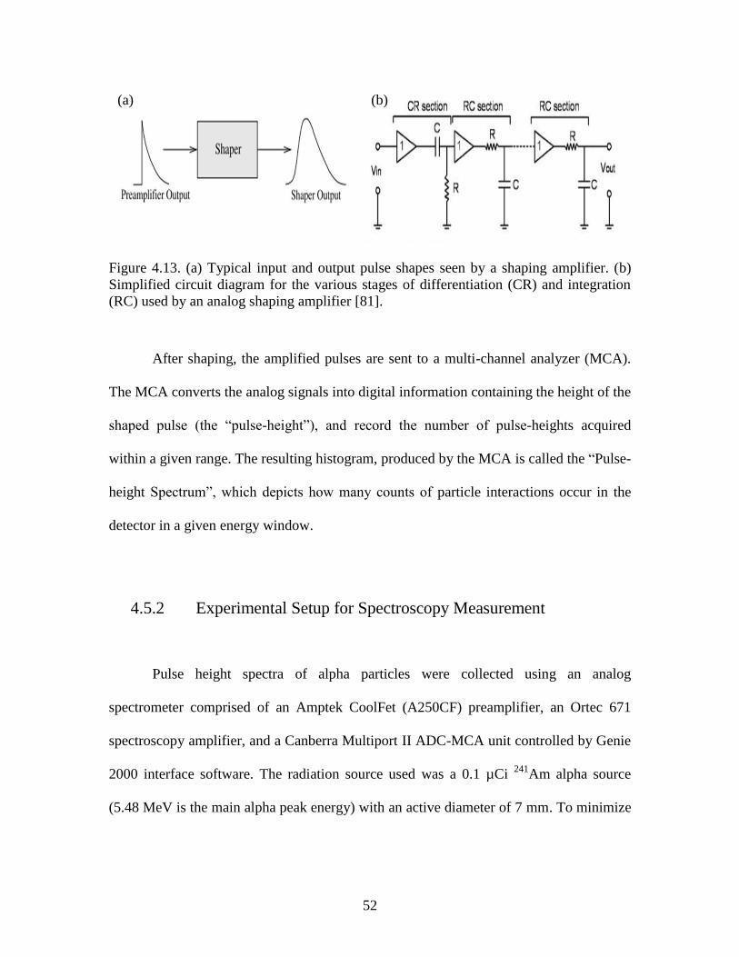
52
Figure 4.13. (a) Typical input and output pulse shapes seen by a shaping amplifier. (b)
Simplified circuit diagram for the various stages of differentiation (CR) and integration
(RC) used by an analog shaping amplifier [81].
After shaping, the amplified pulses are sent to a multi-channel analyzer (MCA).
The MCA converts the analog signals into digital information containing the height of the
shaped pulse (the “pulse-height”), and record the number of pulse-heights acquired
within a given range. The resulting histogram, produced by the MCA is called the “Pulse-
height Spectrum”, which depicts how many counts of particle interactions occur in the
detector in a given energy window.
4.5.2 Experimental Setup for Spectroscopy Measurement
Pulse height spectra of alpha particles were collected using an analog
spectrometer comprised of an Amptek CoolFet (A250CF) preamplifier, an Ortec 671
spectroscopy amplifier, and a Canberra Multiport II ADC-MCA unit controlled by Genie
2000 interface software. The radiation source used was a 0.1 µCi 241
Am alpha source
(5.48 MeV is the main alpha peak energy) with an active diameter of 7 mm. To minimize
(a) (b)

53
electromagnetic interference with the detector, the source and the detector under test were
mounted inside an RFI/EMI shielded aluminum box.
During the measurements, the box was constantly evacuated (~10-3
mbar) using a
rotary pump in order to minimize the scattering of alpha particles with air molecules. The
radiation source was mounted inside the box just above the detector (facing the Schottky
contact) at a vertical distance of 12 mm which ensures a full window illumination. Figure
4.14 shows a photograph of the 4H-SiC epitaxial Schottky barrier radiation detector
inside the RFI/EMI shielded test box.
Figure 4.14. Photograph of the 4H-SiC epitaxial Schottky barrier radiation detector inside
RFI/EMI shielded test box.

54
After placing the detectors and the sources in a proper configuration in the test
box, the connections between the detector box, the pre-amplifier (A250CF), the NIM bin,
the oscilloscope, and the computer were made as shown in Figure 4.15.
Figure 4.15. Connection schematic for analog data acquisition set-up.
The charges generated in the detector due to the incident radiation energy are
collected by the A250CF, which is a charge sensitive low noise pre-amplifier and is best
suited for room-temperature detector operation. It hosts a Peltier cooled FET which helps
with noise reduction to a great extent. The voltage output of the pre-amp is then fed to the
shaping amplifier (Ortec 671) which produces a shaped (semi-Gaussian) amplified output
with enhanced signal-to-noise ratio. This is achieved by using a band pass filter
consisting of differentiator and integrator circuits. The amplifier allows the user to select
the shaping time constant for optimized (trade-off between minimum noise and complete

55
charge collection time) detector performance. This amplified voltage output is directly
proportional to the incident energy of the radiation.
The amplified output pulse is then fed to a multichannel analyzer (MCA), which
basically digitizes the amplifier output pulse signal, and bins the pulses of similar heights
in similar bins or channels to obtain a histogram of the distribution of pulse-height. A
higher channel number corresponds to a higher energy level. The resulting distribution is
called a pulse-height spectrum or simply energy spectrum. Once a pulse-height spectrum
is generated, the full width at half maxima (FWHM) of the alpha energy peak is
calculated through the Gaussian peak fitting function using the Origin plotting software.
The energy resolution of the detector is calculated by the following Equation 4.4:
% 𝐸𝑛𝑒𝑟𝑔𝑦 𝑅𝑒𝑠𝑜𝑙𝑢𝑡𝑖𝑜𝑛 =𝐹𝑊𝐻𝑀 (𝑘𝑒𝑉)
𝐶𝑒𝑛𝑡𝑟𝑜𝑖𝑑 (𝑘𝑒𝑉)∗ 100% 4.4
where the centroid is the “center of mass” of the energy peak observed in the
pulse-height spectrum. Lower values of energy resolution and FWHM indicate better
detector performance. The software Genie 2000 was used to acquire and save pulse-
height spectra and also to analyze the acquired data.

56
Figure 4.16. Schematic of the electrical connections for energy calibration.
Once the data is acquired, a calibration process is performed in order to find a correlation
between the channels of the MCA with their corresponding energy. It is important to note
that the calibration process should be done under the same settings and similar
configuration as the setup used to test a radiation detector. In order to calibrate the
system, a pulser, which generates waveforms and simulates the output of a radiation
detector, is connected to the detection system through a capacitor. Figure 4.16 shows the
connection schematic for energy calibration. The energy of the charge pulses from the
capacitor, Epulser (in keV ) can be determined using the Equation 4.5.
𝐸𝑝𝑢𝑙𝑠𝑒𝑟 =𝑉𝑝𝑢𝑙𝑠𝑒𝑟 × 𝜀 × 𝐶
1.6 × 10⁻¹⁹
4.5

57
where ε is the electron-hole pair creation energy (7.7 eV for 4H-SiC) [82]. This
calibration was accomplished by the injecting pulses of various known amplitudes, Vpulser
(mV), from a precision pulser (Ortec 419) through a calibrated feed-through capacitor, to
the preamplifier input and simultaneously noting down the peak positions of the shaped
pulses in the MCA.
Figure 4.17. (a) Pulse-height spectrum obtained for six different pulse sizes, and (b)
Corresponding calibration curve.
The pulse-height is systematically changed via the pulser to generate several peak
positions relative to the pulser energies. A graphical plot between 𝐸𝑝𝑢𝑙𝑠𝑒𝑟 and
corresponding MCA peak positions for different pulse-heights, gives the calibration
graph. Figure 4.17 shows one MCA spectrum with various pulser peak-positions taken
during calibration. The linear plot of the peak centroid channel number against the keV
equivalent pulser energy as shown in Figure 4.0 b gives the required calibration
parameters [83]. Using the Equation 4.5, values obtained in terms of MCA channel
(a
) (b
)

58
numbers are converted to energy units in keV. The entire radiation detection setup in our
laboratory at USC is shown in the Figure 4.18.
Figure 4.18. Picture of the radiation detection system at USC.
4.6 ALPHA SPECTROSCOPY MEASUREMENT RESULTS
The information obtained by the electrical characterization of the fabricated
detectors is useful deciding which detectors are suitable for spectroscopic
characterization. Spectroscopic characterization was performed using the detector AD06
and a 0.1 µCi 241
Am alpha source. The spectrometer was set up following the description
in Section 4.5.

59
Figure 4.19 shows the variation of charge collection efficiency (CCEobs) for alpha
particles calculated from detector AD06 as a function of reverse bias [75]. The CCEobs
was calculated as the ratio of the output energy observed by the detector to the actual
incident energy of the alpha particles (5.48 MeV). The contribution of the drift
(CCEdepletion) and diffusion (CCEdifussion) related charge collection to the observed total
charge collection efficiency was calculated using the drift-diffusion model described in
section 4.3.
The detector readily showed an alpha peak with charge collection efficiency
(CCE) of ~17% at 0 V applied bias when exposed to a 241
Am source, suggesting a
substantial diffusion of minority carriers. As can be seen from Figure 4.19, the charge
collection efficiency was observed to improve with increase in reverse bias.
Figure 4.19. Variation of experimentally ob ○)
CCE. CCE from drifts (∆) and diffusion (∇) are also shown. The solid line shows the
variation in depletion width.

60
From Figure 4.19 it could be seen that the experimentally observed CCE values
reached a maximum value of ~0.87 at an applied bias of 130 V and started to decrease
slowly thereafter. A CCE value less than 1 suggests that a fraction of the generated
charge carriers are getting trapped and eventually lost (recombine) in the defect centers. It
can also be noticed from Figure 4.19 that the major contribution towards the observed
CCE was from the diffusion of the charge carriers (more than 50%). The contribution of
the drifting of charge carriers (𝐶𝐶𝐸𝑑𝑒𝑝𝑙𝑒𝑡𝑖𝑜𝑛) towards CCEobserved was seen to increase
steadily with the reverse bias and became almost equal to 𝐶𝐶𝐸𝑑𝑖𝑓𝑓𝑢𝑠𝑖𝑜𝑛 at higher reverse
bias voltages. The reason behind the dominating contribution of charge carrier diffusion
towards CCEobserved is because of the fact that the depletion width (~10 µm) at the highest
applied bias of -180 V was still much less compared to the penetration depth of the 5486
keV alpha particles (~18 µm) in 4H-SiC. Hence, a substantial part of the charge carrier
generation takes place in the neutral region of the detector. However, for superior
detector performance, the generation of charge carriers is preferred to occur in the
depletion region in order to obtain optimized charge transport properties. The reverse bias
was further increased to widen the depletion width so that the contribution of charge
carrier drifting in the detector could increase CCE. However, further increase in bias
voltage led to increased leakage currents which deteriorated the detector performance.
The depletion width (d) of a Schottky junction of a given material and bias
depends on the effective doping concentration of the semiconductor material as shown in
Equation. 4.6. Electrically active defects can behave as acceptor or donor levels thus
controlling the effective doping concentration and hence the depletion width.

61
𝑑 = √2𝜀𝜀𝑟(∅𝐵 − 𝑉)
𝑞𝑁𝑒𝑓𝑓 4.6
Figure 4.20. Variation of detector energy resolution as a function of reverse bias voltage.
The variation of the peak width (FWHM) of the pulser recorded simultaneously has also
been plotted.
The dependence of detector energy resolution with the reverse bias is shown in
Figure 4.20 [75]. The percentage energy resolution improved with the reverse bias
because of improved charge collection and lowering of detector capacitance (reduction of
series noise). However, the resolution was seen to deteriorate with further increase in
reverse bias due to increase in leakage current as was evident from the increase in the
corresponding pulser peak width (FWHM) shown along-with in Figure 4.20. Also,
increase in the depletion width leads to inclusion of more number of defects within the

62
detector active volume leading to poor performance of the detectors. Figure 4.21 shows
the best pulse-height spectrum obtained with the optimized bias settings. The energy
resolution of 1.8% is observed for the 5486 keV alpha peak [75].
Figure 4.21. An
241Am pulse-height spectrum obtained using the 50 µm n-type Ni/4H-
SiC epitaxial Schottky barrier detector reverse biased at 130 V.
The pulse-height spectra for 241
Am obtained from detectors AS1, AS2, and AS3
are shown in Figure 4.22 (a), (b), and (c), respectively [2]. The percentage energy
resolutions of the detectors AS1, AS2, and AS3 were calculated as 0.29% , 0.38% and
0.96%, respectively. Detector AS1 exhibited the highest energy resolution (0.29%)
among the three detectors, and it could be seen from Figure (a) that the three major alpha
particle energies, viz. 5388 keV, 5443 keV, and 5486 keV emitted from an 241
Am source
were clearly resolved. Detector AS2 showed a moderately high energy resolution of
0.38%, and AS3 showed a comparatively lower resolution but still less than 1% for 5486
keV alpha particles.

63
Figure 4.22. Alpha pulse-height spectra obtained for detectors (a) AS1, (b) AS2,and (c)
AS3 using an 241
Am source.

64
4.7 CONCLUSION
Electrical and spectroscopic characterizations were performed on 4H-SiC
detectors fabricated on 20 m and 50 m n-type 4H-SiC epilayers. I-V characteristics
revealed the Schottky behavior of the detectors. Using a thermionic emission model, the
barrier height and diode ideality factor were calculated for all fabricated detectors. The
doping concentration (Neff) was calculated from the C-V measurements. Due to good
Schottky behavior and low leakage current at high reverse bias voltage (>100 V) the
fabricated detectors were found to be suitable for radiation detection. Spectroscopic
characterization was performed on the detectors with 241
Am alpha source. The percentage
energy resolution of the detectors was found in the range 0.29% - 1.8% for 5486 keV
alpha particle peak.

65
CHAPTER 5: DEFECT CHARACTERIZATION BY DLTS STUDIES
5.1 INTRODUCTION
In a semiconductor material, defect centers could either act as an electron trap or a
hole trap. These trap levels are associated with four fundamental phenomena that may
occur as illustrated in Figure 5.1. Electrons could be trapped by a defect level acting as an
electron trap. This process is known as electron capture. Consequently, a trapped electron
may get de-trapped if sufficient thermal energy is available. This process is known as
electron emission. Similarly, a hole capture process is characterized by trapping of a hole
by a defect level and the hole emission process by de-trapping of a previously captured
hole.
The semiconductors properties may be greatly influenced due to this charge
carrier capture/emission phenomena by the defects and hence affect the efficiency of the
electronic devices. Therefore, it is very important to identify and characterize the defects
to understand their role in electronic and opto-electronic device performance. The
characterization would provide a deep understanding of defects in the semiconductor
which will be very helpful to enhance the efficiency of devices.

66
Figure 5.1. Illustration of electron and hole trapping and de-trapping phenomena in a
semiconductor material.
Different techniques have been used to characterize the defects in semiconductor,
some of which include: admittance spectroscopy (AS), positron annihilation spectroscopy
(PAS), thermally stimulated current (TSC), Rutherford backscattering spectroscopy
(RBS), optically stimulated conductivity (OSC), thermally stimulated capacitance
(TSCAP), and deep level transient spectroscopy (DLTS). In this chapter, the theoretical
background and experimental methods of defect characterization by TSC and DLTS are
discussed in detail.
Valence Band
Conduction Band
EC
ET,n
EV
Electron capture
cn
Electron emission
en
Hole capture
ch
Hole emission
eh
e-
h+
Eg
ET,h

67
5.2 DEFECT PARAMETERS
During defect characterization, by any method, it is essential to measure some of
the important parameters of the defects. The main parameters required for
characterization of deep levels are: (a) Activation energy, (b) Capture cross-sections, (c)
Concentration of deep levels.
5.2.1 Energy Level
The activation energy ∆E gives the exact position of a deep level in the band-gap.
The activation energy of defects is defined as the required energy needed to move an
electron from the trap center into the appropriate energy band. The activation energy of a
defect depends upon the location of the trap center in the band-gap and varies from defect
to defect. The energy of the conduction band Ec or energy of the valence band Ev is
usually taken as reference during the measurement of the activation energy. A trap with
the energy ET in the band-gap requires the activation energy (Ec- ET) for electron
emission and (Ev + ET) for hole emission.
5.2.2 Trap Concentration
Trap concentration is one of the most important parameters for defect
characterization. Defect properties and their influence on semiconductor behavior greatly
depend on their concentration. This parameter helps to determine the extent of the role
68
defects have on device performance. The trap concentration is defined as the amount of a
particular deep level in the band-gap of the semiconductor material. The number of deep
level traps in the band-gap of the semiconductor material is denoted as the concentration
of deep levels.
5.2.3 Capture Cross-section
Deep levels may act as a trapping, recombination, or generation centers in the
semiconductors. Each of these behaviors highly depend upon the electron and hole
capture rates of the trap. The capture rate of a trap is determined by the characteristics of
the capture cross-section for that particular trap.
5.3 DEFECT CHARACTERIZATION BY THERMALLY STIMULATED CURRENT
5.3.1 Background and Experiment
Thermally stimulated current (TSC) is widely used to study deep energy levels in
semiconductor materials [49]. In TSC measurement, the semiconductor is cooled to a low
temperature, and the trap centers are filled using light of a wavelength greater than or
equal to the band-gap of the material. The electrons/holes are emitted from the filled traps
by slowly heating the sample at a constant rate. Under an applied bias, the emitted
electrons and holes will produce current which is measured by an ammeter and a PC. The
emission is thermally activated and has an emission rate en [84] given by
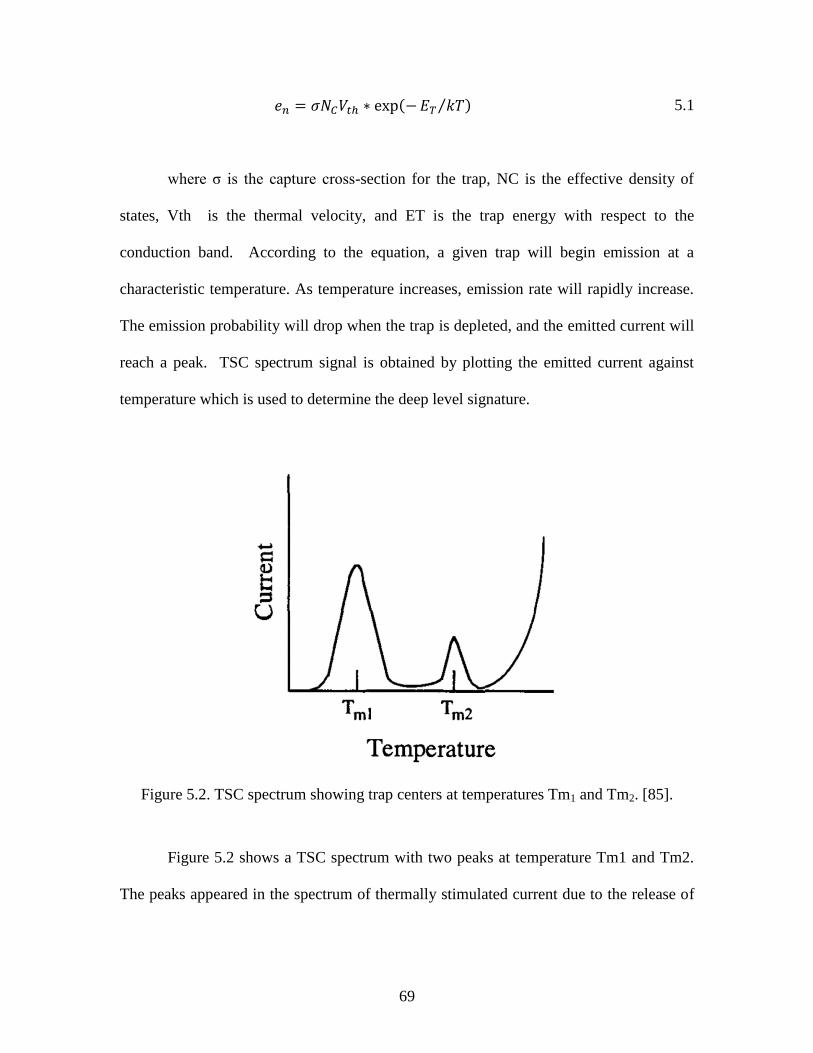
69
𝑒𝑛 = 𝜎𝑁𝐶𝑉𝑡ℎ ∗ exp (− 𝐸𝑇 𝑘𝑇⁄ ) 5.1
where σ is the capture cross-section for the trap, NC is the effective density of
states, Vth is the thermal velocity, and ET is the trap energy with respect to the
conduction band. According to the equation, a given trap will begin emission at a
characteristic temperature. As temperature increases, emission rate will rapidly increase.
The emission probability will drop when the trap is depleted, and the emitted current will
reach a peak. TSC spectrum signal is obtained by plotting the emitted current against
temperature which is used to determine the deep level signature.
Figure 5.2. TSC spectrum showing trap centers at temperatures Tm1 and Tm2. [85].
Figure 5.2 shows a TSC spectrum with two peaks at temperature Tm1 and Tm2.
The peaks appeared in the spectrum of thermally stimulated current due to the release of

70
charge carriers from two different trap centers in the band-gap [49]. The thermally
stimulated current can be described by the following equation [84, 85]
𝐼𝑇𝑆𝐶 = 𝐶𝑉𝑏𝑞𝜇𝜏𝑁𝑇𝑒𝑛 ∗ exp (− ∫𝑒
𝛽d𝑇) 5.2
where q is electronic charge, µ is the carrier mobility, τ is the carrier lifetime, NT
is the trap density, Vb is the bias voltage, en is the emission rate of trapped carriers, β is
the heat rate, and C is the constant related to the sample geometry.
The magnitude of a peak corresponding to a trap center in a given spectrum will
vary with the heating rate. An Arrhenius plot can be drawn from the peaks of different
heating rate spectrum, and all of these peaks are associated with a particular trap. The
trap center activation energy associated with peaks at Tm can be calculated from the
slope of an Arrhenius plot using equation [84, 85, 86],
𝐸𝑇
𝑘𝑇= ln (
𝑇𝑚4
𝛽) + ln (
1017∗𝜎
𝐸𝑇) 5.3
where ET is the activation energy of the trap level, β is the heating rate, σ is the
capture cross-section, and k is the Boltzmann’s constant.

71
Figure 5.3. Schematic of the TSC experimental setup
The TSC measurements on the epitaxial layers were conducted in the temperature
range 94 K - 620 K in vacuum of about 2×10⁻⁵
Torr. Figure 5.3 shows the schematic of
the experiment setup for TSC measurement. The setup is equipped with a Keithley
6517A Electrometer/High resistance meter, thermal stage with programmable
temperature controller (MMR Technologies), and low temperature microprobe (LTMP)
chamber. At 94 K, the traps are filled by illumination using an UV lamp (320 nm, 1.5
mW/cm2) [86].
5.3.2 TSC Spectroscopy and Defect Identity
For TSC measurement the 8 mm × 8 mm samples were taken from a ~ 390 µm
thick 4H-SiC (0001) semi-insulating wafer with a resistivity ≥ 1012 Ω-cm. After standard
RCA cleaning, Ni contacts on both Si and C side were deposited by electron beam
deposition. The contacts were annealed at 1273 K for 1 minute in nitrogen ambient using
SiC V-source
PC
A
Ni
Thermal stage
Ni
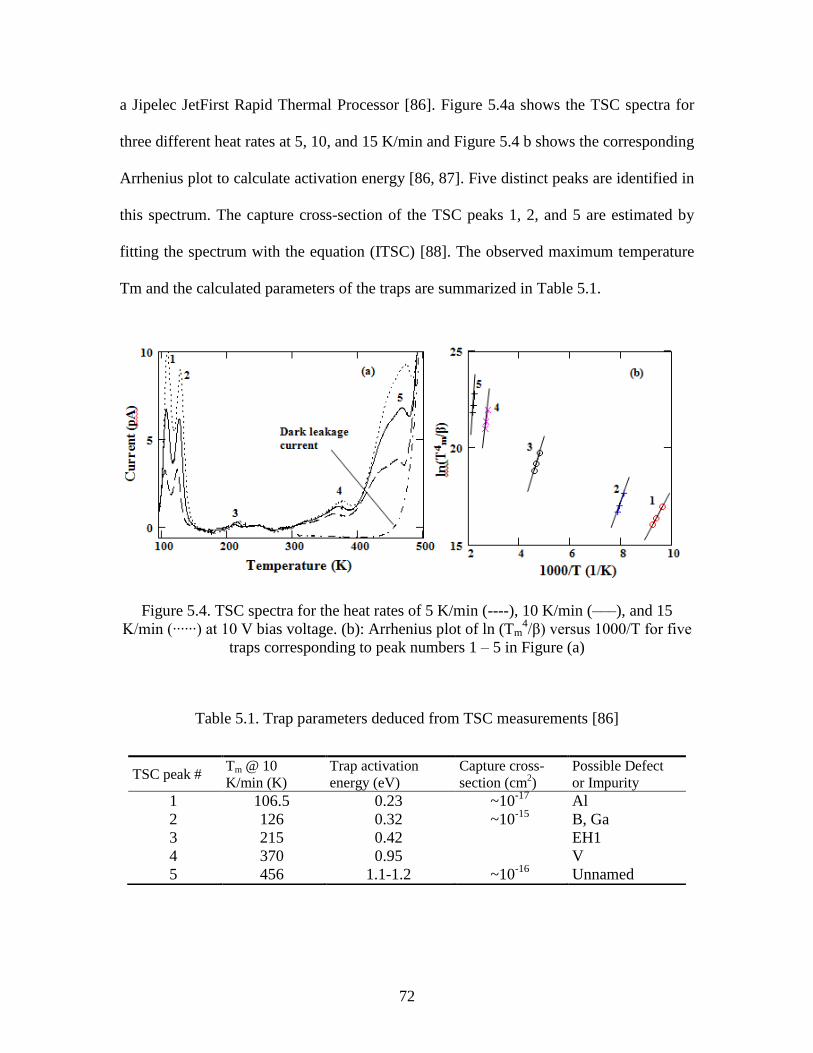
72
a Jipelec JetFirst Rapid Thermal Processor [86]. Figure 5.4a shows the TSC spectra for
three different heat rates at 5, 10, and 15 K/min and Figure 5.4 b shows the corresponding
Arrhenius plot to calculate activation energy [86, 87]. Five distinct peaks are identified in
this spectrum. The capture cross-section of the TSC peaks 1, 2, and 5 are estimated by
fitting the spectrum with the equation (ITSC) [88]. The observed maximum temperature
Tm and the calculated parameters of the traps are summarized in Table 5.1.
Figure 5.4. TSC spectra for the heat rates of 5 K/min (----), 10 K/min (–––), and 15
K/min (∙∙∙∙∙∙) at 10 V bias voltage. (b): Arrhenius plot of ln (Tm4/β) versus 1000/T for five
traps corresponding to peak numbers 1 – 5 in Figure (a)
Table 5.1. Trap parameters deduced from TSC measurements [86]
TSC peak # Tm @ 10
K/min (K)
Trap activation
energy (eV)
Capture cross-
section (cm2)
Possible Defect
or Impurity
1 106.5 0.23 ~10-17
Al
2 126 0.32 ~10-15
B, Ga
3 215 0.42 EH1
4 370 0.95 V
5 456 1.1-1.2 ~10-16
Unnamed
73
The intrinsic defects of 4H-SiC, which are responsible for the TSC peaks, are
identified by using literature data. Maximum temperature and activation energy of the
peaks in the TSC spectrum are compared with those of published literature to identify the
impurity causing the defects. The peak 1 maximum temperature and activation energy is
similar to that found by Fang et al. [84], and they assigned the peak to aluminum related
shallow hole trap. Lebedev et al. [89] showed that boron or gallium related shallow hole
trap and EH1 electron trap are responsible for the peaks 2 and 3 of the spectrum. The
peak 4 is identified as electron trap related to vanadium acceptor level [84]. The
activation energy of peak 5 of the spectrum is found in the range of 1.1 eV - 1.2 eV. Deep
levels with this activation energy were found for bulk semi-insulating SiC [90, 91].
However, the origin of the defect is unknown, and no name is assigned to it.
In another experiment, TSC measurement was carried out on n-type 4H-SiC
epitaxial layers grown by chemical vapor deposition (CVD). Figure 5.5 shows the TSC
spectrum of the samples obtained with 15 K/min heat rate at 10 V reverse bias [92]. All
the parameters extracted from the TSC measurement are provided in Table 5.2.
The peak #1 of the spectrum is due to B/Al complexes which form shallow
acceptor-like levels near the valence band edge [93]. The peak #2 appeared at Tm ~ 175
K in the spectrum. This peak is due to hole traps in the lower half of the band-gap and
identified as HS1 [94] and HH1 [95]. Peak #3 observed at ~ 225 K in the spectrum and is
associated with boron related D-center [84, 89, 96]. Peak #4 (Tm ~ 280 K) is attributed to
Z1/2 which is an electron trap associated with a vacancy related defect [89, 94]. Broad

74
peak #5 (350 – 400 K) can be associated with IL2 [97], SI-6 [98], and SI-8 [98] intrinsic
defects. However, a V-related trap center was also identified as the origin of peak #5 [84,
86].
Figure 5.5. TSC spectrum of n-type 4H-SiC epitaxial layer obtained at 10 V reverse bias
and 15 K/min heat rate [92].
Table 5.2. Trap parameters by TSC measurements for the 4H-SiC n-type epilayer [92]
Sample TSC Peak # Trap activation
energy (eV)
Capture cross-
section (cm2)
Possible Defects or
Impurities
1 0.22 ~10-16
Al/B complexes, shallow
2 0.25 ~10-15
HS1-HH1 Hole traps
4H-SiC 3 0.31 ~10-16
Boron D center
n-type epilayer 4 0.95 Z1/2 electron center
5 - IL2, SI-6, SI-8 and/or
to V

75
5.4 THEORETICAL BACKGROUND OF DLTS MEASUREMENT
5.4.1 Introduction
Deep levels influence both the electrical and the optical properties of material
which can severely affect the device performance. It is very essential to develop sensitive
equipment for deep level characterization semiconductor material. The equipment should
be able to determine all important parameters (energy level, concentration, and capture
cross-section) of the defects. It is also preferable that the equipment can distinguish
between majority and minority carrier traps. Deep level spectroscopy (DLTS) is one of
the most versatile techniques to determine the abovementioned electrical properties of
electrically active defects over a wide range of depths in semiconductor material.
DLTS investigates electrically active defects in a depletion region of Schottky
diodes or p-n junctions. In the DLTS measurement process, the depletion region is kept in
reverse bias condition with a steady-state voltage. The depletion region reduction by a
voltage pulse allows the flow of charge carriers (electron/holes) from the bulk region to
the depletion region which fills the defect centers. When the pulse is removed, the defects
start to emit trapped carriers due to thermal emission which causes transients in the
depletion region capacitance. Important defect parameters can be determined by
analyzing these capacitance transients. The DLTS, which is the most sensitive defect
characterization technique, was first introduced by D. V. Lang (David Vern Lang of Bell
Laboratories) in 1974 [14].

76
5.4.2 DLTS Technique
The DLTS measures the change of junction capacitance of the sample due to the
emission of charge carriers from the defects existing in the space charge region. To better
understand the DLTS theory, let us consider a reverse biased n-type semiconductor
Schottky device as shown in Figure 5.6 A. The depletion region capacitance of a
Schottky device having a homogeneous doping concentration can be expressed as
𝐶0 = 𝐴√𝜀𝜖0 𝑒𝑁𝐷
2(𝑉𝑟 + 𝑉𝑑) 5.4
where A is the sample area, ND is the charge density in the space charge region,
Vr is the reverse bias, Vd is the built-in voltage is the permittivity of the semiconductor
material, and e is the electron charge.
The semiconductor has a deep level trap with energy ET, and all the traps in the
space charge region are empty whereas all the traps in the bulk semiconductor are filled.
An applied pulse (Figure 5.6 B) reduces the space charge width and increases the
capacitance drastically. Now the traps are filled with the injected carriers from the bulk
region. With return of the reverse bias to its quiescent level, the width of the space charge
region increases again (Figure 5.6 C). However, charge density in the space charge region
is slightly less than it was before applying the pulse. Therefore, the width of the space
charge region, in the case of Figure 5.6 C, is slightly higher than that of Figure 5.6 A.
Obviously; the capacitance is slightly lower for the case C.
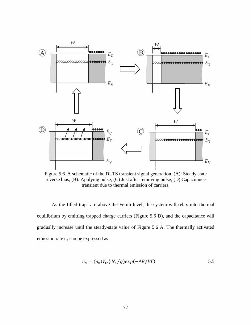
77
Figure 5.6. A schematic of the DLTS transient signal generation. (A): Steady state
reverse bias, (B): Applying pulse; (C) Just after removing pulse; (D) Capacitance
transient due to thermal emission of carriers.
As the filled traps are above the Fermi level, the system will relax into thermal
equilibrium by emitting trapped charge carriers (Figure 5.6 D), and the capacitance will
gradually increase until the steady-state value of Figure 5.6 A. The thermally activated
emission rate en can be expressed as
𝑒𝑛 = (𝜎𝑛⟨𝑉𝑡ℎ⟩ 𝑁𝐶 𝑔⁄ )𝑒𝑥𝑝(−∆𝐸 𝑘𝑇⁄ ) 5.5

78
where σn is the carrier capture cross-section, ⟨Vth ⟩ is the mean thermal velocity,
NC is the effective density of states, g is the degeneracy of the trap level and was
considered to be equal to 1 in the present calculations, and ∆E is the energy separation
between the trap level and the carrier band.
Figure 5.7. The applied bias and the capacitance change of the Schottky device as a
function of time.
The periodic applied pulse and the corresponding periodic capacitance transient
are shown in Figure 5.7. The capacitance transient is related to the emission rate by the
following relationship:
𝐶(𝑡) = 𝐶𝑜 + ∆𝐶 exp(−𝑡𝑒𝑛) 5.6

79
where C0 is the junction capacitance at steady-state reverse bias voltage and ∆C is
the difference in capacitance between case A and case C (difference in capacitance
change between the two edges of the filling pulse) and can be expressed as
∆𝐶 = 𝐴√𝜀𝜖0 𝑒𝑁𝐷
2(𝑉𝑟 + 𝑉𝑑)− 𝐴√
𝜀𝜖0 𝑒 (𝑁𝐷 + 𝑁𝑡)
2(𝑉𝑟 + 𝑉𝑑) ≅ 𝐶0
𝑁𝑡
2𝑁𝐷 5.7
where Nt is the trapping density. The trap concentration Nt is expressed as,
𝑁𝑡 = 2 (∆𝐶𝐶0
⁄ ) 𝑁𝐷 5.8
5.4.3 DLTS Signal Analysis
The DLTS spectrum is generated from the capacitance transient of Figure 5.7 by
applying correlation techniques. The simplest kind of correlation is a dual gate (double
boxcar) with gates set at t1 and t2 proposed by Lang [14] where the capacitance is
measured at two times t1 and t2 after the end of each filling pulse. The DLTS signal is
expressed as
𝑆 = 𝐶(𝑡1) − 𝐶(𝑡2) 5.9
The DLTS starts at low temperature and is recorded by slowly ramping up the
temperature. At low temperature, the capacitance transient is slow due to low thermal
emission, and the DLTS signal is very small as shown in Figure 5.8 (i). With the increase

80
of temperature, the decay rate of the capacitance transient increases. Therefore, the
difference between the capacitance at times t1 and t2 become greater which result in a
larger value of the DLTS signal. This increase of DLTS signal continues with
temperature until most of the transient decay takes place which is before time t1 as shown
in Figure 5.8 (ii - vi). After that temperature, the DLTS signal starts to decrease with
further increase of temperature as shown in Figure 5.8 (vii - ix). When the temperature is
too high, the capacitance transient ends before time t1, and the DLTS signal is zero as
shown in Figure 5.8 (x). A peak is reveal when the DLTS signal is plotted as function of
sample temperature.
The DLTS peak appearance depends upon the selection of t1 and t2 which is
termed as “rate window” selection. In DLTS, thermal scan peaks appear only when the
trap emission rate falls into the rate window. For a given rate window, a DLTS peak
related to a trap with a higher emission rate will move to higher temperature. Since the
emission rate is strongly temperature dependent, peak related to a trap’s level will appear
when its emission rates coincide with the rate window. Hence, in DLTS, peaks
corresponding to different traps appear as a function of temperature as shown in Figure
5.9. Signals from different defect levels can be resolved in a single DLTS scan.
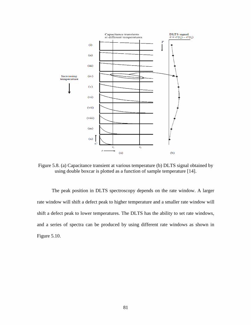
81
Figure 5.8. (a) Capacitance transient at various temperature (b) DLTS signal obtained by
using double boxcar is plotted as a function of sample temperature [14].
The peak position in DLTS spectroscopy depends on the rate window. A larger
rate window will shift a defect peak to higher temperature and a smaller rate window will
shift a defect peak to lower temperatures. The DLTS has the ability to set rate windows,
and a series of spectra can be produced by using different rate windows as shown in
Figure 5.10.

82
Figure 5.9. An illustration of how a rate window produces a peak in its response when the
emission rate of the input signal matches the rate selected by the window [14].
Figure 5.10. (a) The DLTS spectra corresponding to a trap center at various rate windows
and (b) the Arrhenius plots obtained from the spectra.

83
The time constant at maximum height of a DLTS peak can be expressed as
𝜏𝑚𝑎𝑥 =𝑙𝑛(𝑡2 𝑡1⁄ )
𝑡2 − 𝑡1. 5.10
In a DLTS thermal scan, the emission rate at the maximum of a trap peak is a
uniquely defined quantity. For each spectrum, the temperature at the maximum peak
height can be measured, and the corresponding emission rate en is calculated via using
Equation 5.10. By using the maximum height of each spectrum, the Arrhenius plot
(log(e/T2) vs. 1000/T), corresponding to a particular trap center, can be drawn as shown
in Figure 5.10 b. The signature of a trap (i.e. activation energy and capture cross-section)
can be extracted from the Arrhenius plot and can be used for defect identification.
5.5 DLTS EXPERIMENTAL SETUP
The DLTS measurements are carried out using a SULA DDS-12 modular DLTS
system. The system is comprised of a pulse generator, a capacitance meter, a correlator
module, and a PC based data acquisition and analysis software. The block diagram and
the photograph of the DLTS system are presented in Figure 5.11 and
Figure 5.12, respectively.

84
Figure 5.11. Block-Diagram of the SULA DDS-12 DLTS setup.
Figure 5.12. Photograph of the SULA DDS-12 DLTS measurement system.
For the measurement, the device under test (Schottky contact) is mounted on a
specially designed sample holder inside a JANIS VPF800 cryostat as shown in Figure
5.13. The sample holder is equipped with a sapphire disc which isolates the device
electrically but ensures excellent thermal conduction. Tungsten probes are used to
Capacitance Meter
Computer
Temperature Controller
Pulse
Generator
Cryostat
Vacuum Pump

85
connect the device with the measurement circuit. Connection to the back Ohmic contact
was established by placing a piece of copper foil on the sapphire disc. Special care is
taken when lowering the top probe so that it will ensure good electrical connection
without damaging the Schottky contact. To minimize the damage to the Schottky contact
the tips of the probes are kept flat by rubbing with very fine sanding paper.
Figure 5.13. Photograph of the sample holder used in DLTS measurements.
The operating temperature of the Cryostat is controlled by a Lakeshore LS335
temperature controller and can be operated in the temperature range of 80 K - 800 K.
Cryogenic temperature is reached by liquid nitrogen. During DLTS measurements, the
device under test is held in a steady-state reverse bias condition and a pulse is applied
periodically to reduce the reverse bias voltage. Repetitive pulsing to the sample is
86
accomplish by a pulse generator which can generate pulses of magnitude from -12 V to
+12 V and width from 1 µs to pulse repetition period. Usually the pulsing is done to 0 V
from the steady-state reverse bias to fill/populate the majority carrier traps present within
the depletion (space charge) width. The pulse width is large enough to get ensure
saturation trap filling. A self-balancing bridge capacitance meter with a 1 MHz oscillator
is used to measure the transient capacitance.
The system is also comprised of a correlator/pre-amplifier module which
automatically removes DC background from capacitance meter and amplifies the
resultant signal. The correlator module uses a modified double boxcar signal averaging
algorithm and measures the capacitance transient in a given rate window. The rate
windows are defined by an initial delay which is actually a delay set for the emission rate
calculations following the termination of the filling pulse. The initial delay is related to
the rate window τ given by
Initial delay (ms) = 1(4.3 × τ)⁄ . 5.11
The DDS-12 system allows the user to collect four DLTS spectra simultaneously
which corresponds to four different rate windows in a single temperature scan. The
signals were digitized using a NI digitizer card integrated with the DLTS system for live
processing using a PC. The entire system including the modules and the temperature
controller is controlled using a dedicated Labview interface which also allows the user to
analyze the recorded data.
87
5.5.1 DLTS Spectra of Fabricated Detector
Figure 5.14 (a) & (b) shows representative DLTS spectra in the temperature range
of 80 K to 140 K using a smaller set of initial delays, and 80 K to 800 K using a larger set
of initial delays, respectively [75]. The peaks appeared at different temperatures
corresponding to different defect levels. In total, six distinct peaks were observed in the
entire temperature scan range of 80 K - 800 K and are numbered as Peak #1 to #6. The
negative peaks indicate that the detected traps are majority carrier traps (electron traps in
this case).

88
Figure 5.14. DLTS spectra obtained using the 50 µm n-type Ni/4H-SiC epitaxial
Schottky barrier radiation detector (AD06) in a temperature range (a) 80 K - 140 K with
the smallest initial delay (b) 80 K - 800 K with the largest initial delay.
The DLTS spectra also collected for the detectors (AS1, AS2, and AS3)
fabricated on 20 µm 4H-SiC epitaxial layers. Figure 5.15 (a), (b), and (c) shows the
DLTS spectra obtained for samples AS2, AS1, and AS3, respectively [2]. In this
measurement for reverse bias, a steady state voltage of -2 V was applied, and the samples
were pulsed by a 1 ms width, 0 V pulse. Four correlator delays 100 ms, 50 ms, 20 ms,
and 10 ms in the temperature range of 230 K - 790 K were used to obtain the DLTS
spectra. The peaks correspond to a particular defect, but due to the four different

89
correlator delays, they were numbered collectively. The peak numbers are used to specify
the position of the DLTS peaks on the temperature axis with respect to detector AS2.
Detector AS2 showed four DLTS peaks two of which labeled peak #1 and peak #4 were
clearly distinguishable peaks. Peak #2 was of very low intensity whereas peak #3
appeared as a partially resolved shoulder. In the DLTS spectra, it is clear that peak #3 is
the only prominent peak for the detector AS1, and peak#1 and peak#4 have very low
magnitude. The spectra of detector AS3 showed the presence of all the peaks except
peak#2.

90
Figure 5.15. DLTS scan for detectors AS2, AS1, and AS3 showing negative peaks related
to electron traps present in the 4H-SiC epilayer detectors.
5.5.2 Arrhenius Plot of the Spectra
The activation energies are calculated from the Arrhenius plots
(𝑇2 𝑒𝑛⁄ 𝑣𝑠 1000 𝑇⁄ ). Figure 5.16 shows the Arrhenius plot for all the peaks obtained

91
from the DLTS scans. The defect parameters were extracted from the DLTS scans using
the equations described above and are summarized in Table 5.3.
Figure 5.16. Arrhenius plots obtained for the Peaks #1 - #6 corresponding to the DLTS
spectra shown inFigure 5.14.
Table 5.3. Defect parameters of the deep levels for the detector AD06
Peak # σn
cm2
E
eV
Nt
cm-3
Possible Trap
Identity
Peak 1 4.13× 10⁻¹⁵
Ec ˗ 0.13 1.3× 10¹³
Ti (h)
Peak 2 2.50× 10⁻¹⁵
Ec ˗ 0.17 3.6× 10¹³
Ti (c)
Peak 3 3.36× 10⁻¹⁵
Ec ˗ 0.67 1.7× 10¹³
Z1/2
Peak 4 3.73× 10⁻¹⁵
Ec ˗ 1.04 2.1× 10¹³
EH5
Peak 5 3.22× 10⁻¹⁷
Ec ˗ 1.30 7.9× 10¹²
Ci1
Peak 6 1.53× 10⁻¹¹
Ec ˗ 2.40 5.6× 10¹²
Newly
identified

92
Figure 5.17. Arrhenius plots for determining the activation energy obtained from the
DLTS scans shown in Figure 5.15 for detectors (a) AS2, (b) AS1, and (c) AS3.The solid
lines show the linear fits.

93
The Arrhenius plot corresponding to the DLTS spectra (Figure 5.15) of the 20 µm
epitaxial layer detectors are shown in Figure 5.17. The defect parameters viz., activation
energy, capture cross-section, and trap concentration are calculated for the three detectors
AS1, AS2, and AS3 are listed in the Table 5.4, Table 5.5, and Table 5.6, respectively [2].
Table 5.4. Defect parameters of the detector AS1 obtained from the DLTS scans
Peak # σn
cm2
E
eV
Nt
cm-3
Possible Trap
Identity
Peak 1 0.05 × 10⁻¹⁶
Ec ˗ 0.60 0.09× 10¹²
Z1/2
Peak 3 575× 10-16
Ec ˗ 1.45 1.27× 10¹²
Ci1
Peak 4 68.8× 10⁻¹⁶
Ec ˗ 1.6 0.1× 10¹²
EH6/7b
Table 5.5. Defect parameters of the detector AS2 obtained from the DLTS scans
Peak # σn
cm2
E
eV
Nt
cm-3
Possible Trap
Identity
Peak 1 1.9 × 10⁻¹⁶
Ec ˗ 0.62 3.2× 10¹²
Z1/2
Peak 2 0.1× 10⁻¹⁶
Ec ˗ 0.80 0.09× 10¹²
Vsi+
Peak 3 1.7× 10⁻¹⁶
Ec ˗ 1.31 0.93× 10¹²
Ci1
Peak 4 28.2× 10⁻¹⁶
Ec ˗ 1.6 1.9× 10¹²
EH6/7b
Table 5.6. Defect parameters of the detector AS3 obtained from the DLTS scans
Peak # σn
cm2
E
eV
Nt
cm-3
Possible Trap
Identity
Peak 1 28.8 × 10⁻¹⁶
Ec ˗ 0.66 1.9× 10¹²
Z1/2
Peak 3 22.6× 10⁻¹⁶
Ec ˗ 1.3 65× 1012
Ci1
Peak 4 158× 10-16
Ec ˗ 1.6 1.8× 10¹²
EH6/7b

94
5.5.3 Defect Identification
At first the deep level defects found in the detector (AD06) fabricated on 50 µm
epitaxial layers as shown in the table are identified by comparing with reported literature
data. The trap levels corresponding to Peak #1 and Peak #2 were found to be located at Ec
- 0.13 eV and Ec - 0.17, respectively, where Ec is the conduction band minimum. Both of
the defect levels have been identified as titanium substitutional impurity. Dalibor et al.
[99, 100] have reported two similar defect levels located at Ec - (0.117 ± 0.008) eV and
Ec - (0.160 ± 0.010) eV from DLTS studies of Ti+ implanted 4H-SiC which they
attributed to the ionized titanium acceptor Ti3+
(3d1) residing at hexagonal and cubic Si
lattice sites, respectively. Gelczuk et al. [101] also reported similar trap levels and
assigned them to the Ti impurities at hexagonal and cubic Si lattice sites. Zhang et al.
[102] also assigned a defect level located at Ec - 0.16 eV to a Ti electron trap level.
Castaldini et al. [103] assigned a trap level located at Ec - 0.17 to chromium or titanium
impurities (acceptor like) in hexagonal position.
The trap center related to Peak #3 was found to be located at 0.67 eV below the
conduction band edge. Several groups have reported the presence of a similar defect level
often designated as Z1/2 [104, 105, 106, 107, 108]. However, the exact microscopic
structure is still unknown and several theories exist in the literature regarding the
probable structure of Z1/2 centers. As summarized by Zhang et al. [102], Z1/2 is most likely
related to defect complexes involving equal number of carbon and silicon sites. The
possible structures listed by them, obtained from the existing literatures [95, 104, 109],

95
are silicon carbon vacancy complexes (VSi + VC), antisite complex (SiC + CSi) pairs, or a
pair of an antisite and a vacancy of different atoms. However, their own findings were
more inclined towards a divacancy like structure of the Z1/2 defect. Eberlein et al. [110]
on the other hand, reported that the participation of carbon interstitial with nitrogen can
also form defect levels with similar activation energy. Z1/2 center is also reported to be
responsible for the reduction of carrier lifetime by several authors [101, 111, 112, 113].
The activation energy corresponding to peak #4 was found to be located at 1.04 eV below
the conduction band edge. A defect level reported by Alfieri et al. [114] located at Ec -
1.03 eV and designated as EH5, is the closest match with the peak #4 observed in our
case. Beyer et al. have also detected a similar defect level (Ec - 1.07 eV) in 2.5 MeV
electron irradiated 4H-SiC [115]. EH5 defect has been found in ion irradiated 4H-SiC and
has been attributed to a carbon cluster [95]. The activation energy of peak #5 was found
to be 1.30 eV. Alfieri et al. [114] reported a similar defect center Ci1 in a chlorine
implanted n-type 4H-SiC epitaxial layer. The peak #6 was found to have the highest
activation energy (2.40 eV) among all the defect centers observed in the DLTS scans and
remains unidentified as the corresponding activation energy does not match with any
known defect level in 4H-SiC that has been reported in the literature. The trap
concentrations corresponding to peak #1 - #4 were all of the order of 1013
cm-3
with the
Ti impurity (cubic Si site) being the maximum. Peak #5 and #6 were found to be one
order of magnitude less in concentration.
In this stage, the deep level defects found in the detectors (AS1, AS2, and AS3)
fabricated on 20 µm epitaxial layers were identified. The deep level defects for the

96
detector AS1, AS2, and AS3 are shown in the table, respectively. Four peaks
corresponding to four different defects are found for the detector AS2. The defect related
peak position for the detectors AS1 and AS2 are numbered with respect to the AS2 peak
position.
The DLTS spectra of detector AS2 showed four peaks and are numbered as peak
#1 to peak #4. The calculated parameters of the defects found in the detector AS2 are
summarized in the table. According to the calculated activation energy, the position of
peak #1 was found to be at Ec - 0.62 eV. A similar kind of defect has been identified as
carbon vacancy (Vc) or its complexes in 4H-SiC samples by several workers [104, 105,
106, 107, 108]. This defect level is often designated as Z1/2 center and is regarded as a
potential lifetime killer [111, 112, 113, 102]. The position of the defect related to weak
peak #2 was found to be at Ec - 0.8 eV. A similar defect level was observed by Nava et
al. [108] in neutron irradiated n-type 4H-SiC using photo-induced current transient
spectroscopy and was identified as silicon vacancy in singly positive charge state (Vsi+).
The defect related to peak #2 was found to have a much less concentration of 9×10¹⁰
cm-3
and a low capture cross-section of 1×10-17
cm2 and thus may not have a substantial effect
in defining the detector performance in this case. The position of shouldered peak #3 in
the band-gap was calculated to be at Ec - 1.31 eV. The peak could not be identified with
any known or reported defect level in the literature. Alfieri et al. [114] reported similar
defect level observed in chlorine implanted n-type epitaxial 4H-SiC and labeled it as Ci1.
The position of peak #4 in the band-gap was calculated to be at Ec - 1.6 eV. Nava et al.
[108] identified a similar defect level as Vc and its complex in neutron irradiated n-type

97
4H-SiC using photo-induced current transient spectroscopy. K. Danno et al. [116]
designated a defect center at Ec - 1.55 eV as EH6/7 and related it to carbon vacancies or
carbon-silicon di-vacancies.
For the detector AS1 and AS3 three peaks (peak #1, peak #3, and peak #4) were
found to be related to the same defect levels as found in detector AS2. The defect related
to the peak #2 in the detector AS2 which is identified as Vsi+ is not found in AS1 and
AS3. By comparison of the defect parameters in detectors AS2 and AS3, it can be
observed that the capture cross-sections corresponding to defects related to peak #1, #3,
and #4 in AS3 were significantly higher than those in AS2.The comparison of the defect
parameters in the detectors AS1 and AS2 shows that the detector AS1 has only the high
concentration of the defect Ci1 ( related to peak #3) and has very low concentration of the
defect Z1/2 (related to peak #1) and the defect EH6/7 (related to peak #4).
5.6 DEFECTS’ ROLE ON DETECTOR PERFORMANCE
To determine the defects’ role on the device performance, the detector properties
and electrically active defects are needed to correlate. Important detector properties and
calculated defects’ parameters are summarized in a separate table for each of the
fabricated detectors. Let us first consider the detectors fabricated on 20 µm epitaxial
layers. The summarized properties of the detectors AS1, AS2, and AS3 are shown in the
Table 5.7, Table 5.8, and Table 5.9, respectively.

98
In Table 5.8, it is shown that four deep level defects Z1/2
, Vsi
+, Ci1, and EH
6/7 are
observed in the detector AS2.The resolution of this detector was calculated to be 0.38%.
The resolution of detector AS3 was calculated to be 0.96%. Three deep level defects Z1/2
,
Ci1, and EH6/7
are identified in this detector as shown in Table 5.9. All the defects
identified in AS2 except the defects Vsi
+ are found in AS3. From the comparison of the
defect parameters in detectors AS2 and AS3, it is found that the capture cross-sections of
the defects Z1/2
, Ci1, and EH6/7
in AS3 are significantly higher than those in AS2. This
suggests higher probability of electron trapping in detector AS3 and hence explains the
comparatively poor performance. The deep level defects Z1/2
, Ci1, and EH6/7
are also
identified in the detector AS1 as shown in the Table 5.7. Among all the defects in AS1,
only Ci1 has a much higher concentration compared to the defects Z1/2
and EH6/7
which
are also clear from the high amplitude of the peak #2 in the DLTS spectra of AS1 as
shown in Figure 5.15 in section 5.5. The trap concentration of the defects Z1/2 and EH6/7
in AS1 are found to be one order of magnitude less compared to those found in AS2 and
AS3.The capture cross-section of the defect Ci1 in AS1 is found to be much higher
compared to any other defects among all the samples. However, the superior performance
of detector AS1 indicates that the defect Ci1 does not significantly affect the detector
performance. The above analysis suggests that among the defects identified in these n-
type 4H-SiC 20 µm epitaxial layers the defects Z1/2 (located at Ec - 0.6 eV) and EH6/7
(located at Ec - 1.6 eV) seems have major role in determining the detector performance.

99
Table 5.7. Detector properties and defect parameters for the detector AS1
Detector
Characterization
Defect Parameters
Ideality Factor 1.2 Trap
Identity σ
n (cm
2
) ∆E (eV) Nt (cm
-3
)
ϕB
(eV) 1.6 Z
1/2 0.05× 10
-16
Ec ˗ 0.60 0.09× 10
12
Leakage Current
at - 100 V (pA) 4.3
Nd(cm
-3
) 2.6× 10¹⁴
Ci1 75× 10
-16
Ec ˗ 1.45 1.27× 10
12
Resolution (%) 0.29 EH6/7
68.8× 10⁻¹⁶
Ec ˗ 1.6 0.1 × 10
12
Table 5.8. Detector properties and defect parameters for the detector AS2
Detector
Characterization
Defect Parameters
Ideality Factor 1.09 Trap
Identity σ
n (cm
2
) ∆E (eV) Nt (cm
-3
)
ϕB
(eV) 1.67 Z1/2
1.9× 10⁻¹⁶
Ec ˗ 0.62 3.2× 10
12
Leakage Current
at - 100 V (pA) 6.2 V
si
+ 0.1× 10
-16
Ec ˗ 0.80 0.09× 10
12
Nd(cm
-3
) 3.2× 10¹⁴
Ci1 1.7× 10
-16
Ec ˗ 1.31 0.93× 10
12
Resolution (%) 0.38 EH6/7
1.58× 10⁻¹⁶
Ec ˗ 1.6 1.8× 10
12
Table 5.9. Detector properties and defect parameters for the detector AS3
Detector
Characterization
Defect Parameters
Ideality Factor 1.24 Trap
Identity σ
n (cm
2
) ∆E (eV) Nt (cm
-3
)
ϕB
(eV) 1.15 Z
1/2 28.8 × 10
-16
Ec ˗ 0.66 1.9× 10
12
Leakage Current
at - 100 V (pA) 10
Nd (cm
-3
) 3.0× 10¹⁴
Ci1 22.6× 10
-16
Ec ˗ 1.3 65 × 10
12
Resolution (%) 0.96 EH6/7
158 × 10-16
Ec ˗ 1.6 1.8 × 10
12
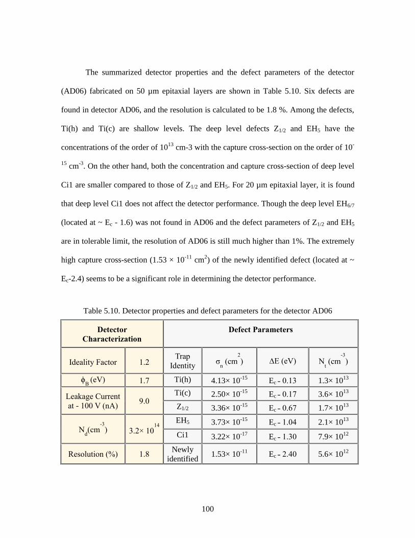
100
The summarized detector properties and the defect parameters of the detector
(AD06) fabricated on 50 µm epitaxial layers are shown in Table 5.10. Six defects are
found in detector AD06, and the resolution is calculated to be 1.8 %. Among the defects,
Ti(h) and Ti(c) are shallow levels. The deep level defects Z1/2 and EH5 have the
concentrations of the order of 1013
cm-3 with the capture cross-section on the order of 10-
15 cm
-3. On the other hand, both the concentration and capture cross-section of deep level
Ci1 are smaller compared to those of Z1/2 and EH5. For 20 µm epitaxial layer, it is found
that deep level Ci1 does not affect the detector performance. Though the deep level EH6/7
(located at ~ Ec - 1.6) was not found in AD06 and the defect parameters of Z1/2 and EH5
are in tolerable limit, the resolution of AD06 is still much higher than 1%. The extremely
high capture cross-section (1.53 × 10⁻¹¹
cm2) of the newly identified defect (located at ~
Ec-2.4) seems to be a significant role in determining the detector performance.
Table 5.10. Detector properties and defect parameters for the detector AD06
Detector
Characterization
Defect Parameters
Ideality Factor 1.2 Trap
Identity σ
n (cm
2
) ∆E (eV) Nt (cm
-3
)
ϕB
(eV) 1.7 Ti(h) 4.13× 10⁻¹⁵
Ec ˗ 0.13 1.3× 10¹³
Leakage Current
at - 100 V (nA) 9.0
Ti(c) 2.50× 10⁻¹⁵
Ec ˗ 0.17 3.6× 10¹³
Z1/2 3.36× 10⁻¹⁵
Ec ˗ 0.67 1.7× 10¹³
Nd(cm
-3
) 3.2× 10¹⁴
EH5 3.73× 10⁻¹⁵
Ec ˗ 1.04 2.1× 10¹³
Ci1 3.22× 10⁻¹⁷
Ec ˗ 1.30 7.9× 10¹²
Resolution (%) 1.8 Newly
identified 1.53× 10
-11 Ec ˗ 2.40 5.6× 10
12

101
5.7 CONCLUSION
Deep level transient spectroscopy (DLTS) studies were conducted to investigate
the defect levels present in the detectors fabricated on different thickness of 4H-SiC
epitaxial layers. In the fabricated detectors different deep level defects were observed in
the temperature scan range of 80 K - 800 K. Types of observed defects and their
parameters varied widely from detector to detector. In all of the detectors fabricated on
20 µm thick epitaxial layers, deep level defects Z1/2 located at Ec - 0.6 eV, Ci1 located at
Ec - 1.3 eV, and EH6/7 located at Ec - 1.6 eV were revealed by the DLTS measurement.
Among them, two defect levels (electron traps) Z1/2 and EH6/7 related to carbon vacancies
and their complexes mostly affected the detector resolution. Defect level observed at Ec -
1.3 eV was found to not affect the detectors’ performance.
For the case of 50 µm epitaxial layer detector, six different defect centers were
detected in the same DLTS temperature scan range of 80 K - 800 K. Defects were
identified as Ti (h) at Ec – 0.13 eV, Ti (c) at Ec – 0.17 eV, Z1/2 at Ec - 0.67 eV, EH5 at Ec -
1.04 eV, Ci1 at Ec - 1.3 eV, and a newly detected deep level at Ec - 2.4 eV. A Deep level
detected located at Ec - 2.4 eV was identified for the first time and has not been reported
to date. Along with Z1/2 and EH5, the newly identified defect at Ec - 2.4 eV mostly
affected the detector resolution fabricated on 50 µm 4 H-SiC epitaxial layers.

102
CHAPTER 6: ANNEALING BEHAVIOR OF CRYSTALLINE
DEFECTS
6.1 INTRODUCTION
For the annealing behavior studies of SiC crystalline defects, nickel (Ni) Schottky
barrier diodes are fabricated on 50 µm thick n-type 4H-SiC epitaxial layers. Deep level
transient spectroscopy (DLTS) measurements were carried out on the fabricated Schottky
diodes in a wide temperature range from 80 K to 800 K to determine the initial defect
parameters (i.e. defect densities, capture cross-sections, and activation energies) prior to
the first iteration of isochronal annealing. Isochronal annealing of the devices was carried
out over the temperature range from 100 ˚C to 800 ˚C. The defect parameters were then
compared with the initial DLTS scans of the unannealed devices.
6.2 DEEP LEVEL TRANSIENT SPECTRA BEFORE ANNEALING
Schottky barrier diodes were fabricated on 50 µm thick n-type 4H-SiC epitaxial
layers to characterize the initial deep level defects. Parameters of the deep level defects
are determined by the DLTS measurements on the fabricated detectors. Figure 6.1 (a)
shows representative DLTS spectra in the temperature range of 85 K to 130 K using a
smaller set of initial delays, and Figure 6.1 (b) shows DLTS spectra in the temperature

103
range 200 K to 800 K using a larger set of initial delays. The peaks appeared at different
temperatures corresponding to different defect levels. In total, four distinct peaks were
observed in the entire temperature scan range of 85 K - 800 K and are numbered as peak
#1 to peak #4.
Figure 6.1. DLTS spectra obtained using the 50 µm thick n-type Ni/4H-SiC unannealed
epitaxial Schottky barrier in the temperature range: (a) 85 K - 130 K with a smaller set of
initial delays, and (b) 200 K - 800 K with a larger set of initial delays.

104
The negative peaks indicate that the detected traps are majority carrier traps
(electron traps in this case). The activation energy is calculated from the Arrhenius
plots (𝑇2 𝑒𝑛⁄ 𝑣𝑠 1000 𝑇⁄ ). Figure 6.2 shows the Arrhenius plots for all the peaks
obtained from the DLTS scans. The defect parameters were extracted from the DLTS
scans described above and are summarized in Table 6.1.
1 2 2 3 3 4 9 10 11 12
100
101
102
103
104
105 peak #1
peak #2
peak #3
peak #4
T2 /e
n (K
2 s)
103/ Temperature (1/K)
Figure 6.2. Arrhenius plots obtained for the peaks #1 - #4 corresponding to the DLTS
spectra shown
Table 6.1. Defect Parameters Obtained from the DLTS Measurements.
Peak # σn
cm2
ΔE
eV
Nt
cm-3
Possible
Trap Identity
Peak 1 6.62× 10⁻¹⁵
Ec ˗ 0.17 1.7× 10¹³
Ti (c)
Peak 2 3.37× 10⁻¹⁵
Ec ˗ 0.67 7.1× 10¹²
Z1/2
Peak 3 5.56× 10⁻¹⁷
Ec ˗ 1.04 7.1× 10¹²
EH5
Peak 4 2.66× 10⁻¹⁷
Ec ˗ 1.60 3.3× 10¹²
EH6/7

105
6.3 EXPERIMENT FOR ISOCHRONAL ANNEALING STUDIES
An annealing experimental set-up has been assembled at USC for the annealing
studies of the defects. The annealing set-up comprises of a furnace with a temperature
control unit, an oil-free mechanical pump, a turbo-molecular pump, vacuum gauge
controller, and turbo pump controller. The block diagram of the isochronal annealing
experimental set up is shown in Figure 6.3.
Figure 6.3. Block diagram of annealing set up at USC.
For isochronal annealing, a sample is loaded in a quartz ampoule and then
connected to the vacuum system of the annealing experimental set-up as shown in Figure
6.4. After the loaded quartz ampoule was pumped down by the mechanical pump for 30

106
minutes, the turbo pump was turned on to achieve higher vacuum pressure levels. A
Varian Multi-Gauge ionization gauge was used to monitor the vacuum pressure level.
After reaching the vacuum pressure level of 2×10⁻⁷
torr, the ampoule was lowered to the
hot zone of a dedicated single-zone tube furnace to be annealed. The temperature of the
furnace was controlled by a Thermolyne temperature control unit. Moreover, a digital
thermocouple is connected to the ampoule for cross-checking the annealing temperature.
Figure 6.4. Picture of the annealing set up at USC.
After characterization of the initial defects of 4H-SiC epitaxial layer by DLTS
measurement, the Schottky devices are ready for annealing. Before annealing, the top and
bottom nickel contact of the Schottky devices were completely etched off by

107
concentrated nitric acid. Then the samples are annealed for 30 minutes. After annealing at
each temperature, the samples are cleaned by RCA cleaning procedure and Ni Schottky
and Ohmic contacts are deposited for subsequent I-V, C-V, and DLTS measurements.
6.4 ANNEALING STUDIES RESULTS
6.4.1 Electrical characteristics after annealing
Figure 6.5 shows the I-V (current-voltage) characteristics of the fabricated
Schottky barrier devices before and after isochronal annealing at different temperatures.
It is observed that the forward current for an applied voltage beyond the knee voltage is
decreased up to the annealing temperature of 400 C and then increased again till the
temperature of 800 C which is a limit of our isochronal annealing studies. Figure 6.6
shows the reverse bias characteristics of the fabricated Schottky diode and after annealing
at different temperatures. The reverse bias current is almost same up to the annealing of
400 C and increased significantly with annealing at 600 C and 800 C, respectively.
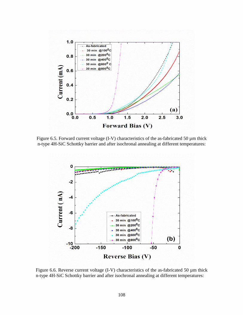
108
Figure 6.5. Forward current voltage (I-V) characteristics of the as-fabricated 50 µm thick
n-type 4H-SiC Schottky barrier and after isochronal annealing at different temperatures:
Figure 6.6. Reverse current voltage (I-V) characteristics of the as-fabricated 50 µm thick
n-type 4H-SiC Schottky barrier and after isochronal annealing at different temperatures:

109
The calculated ideality factor from the forward I-V characteristics is shown in
Figure 6.7. A comparison of the ideality factors of fabricated devices before and after
annealing at different temperatures revealed the presence of spatial non-uniformities in
barrier heights over the metal contact area [117]. The total diode current is an aggregate
of the current flowing through different barrier height regions in the metal semiconductor
interface. Low barrier height turns on at a lower bias than the high barrier height region
and the non-ideality in the diode characteristics arises. The ideality factor of the
unannealed SiC Schottky barrier is significantly higher than ideality factors found after
annealing at different temperatures.
Calculated ideality factor of ~1.6 of the as-fabricated Schottky barrier suggests
the presence of high density patches of small barrier heights [50, 118, 119]. The ideality
factor reduces to ~1.2 after annealing at 100 C, implying the major reduction of the
density of patches. The density of low barrier height patches do not change significantly
with further annealing at higher temperatures which is also clear from the small variation
of ideality factor throughout the annealing studies up to 800 C.
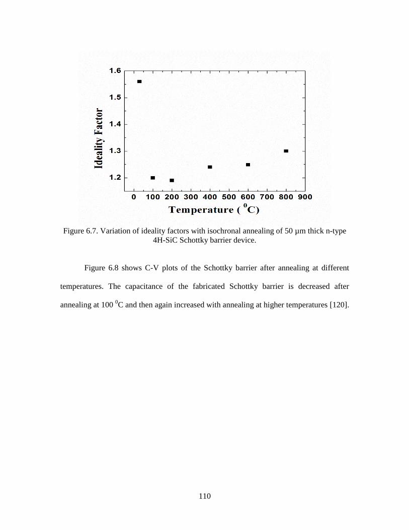
110
Figure 6.7. Variation of ideality factors with isochronal annealing of 50 µm thick n-type
4H-SiC Schottky barrier device.
Figure 6.8 shows C-V plots of the Schottky barrier after annealing at different
temperatures. The capacitance of the fabricated Schottky barrier is decreased after
annealing at 100 0C and then again increased with annealing at higher temperatures [120].
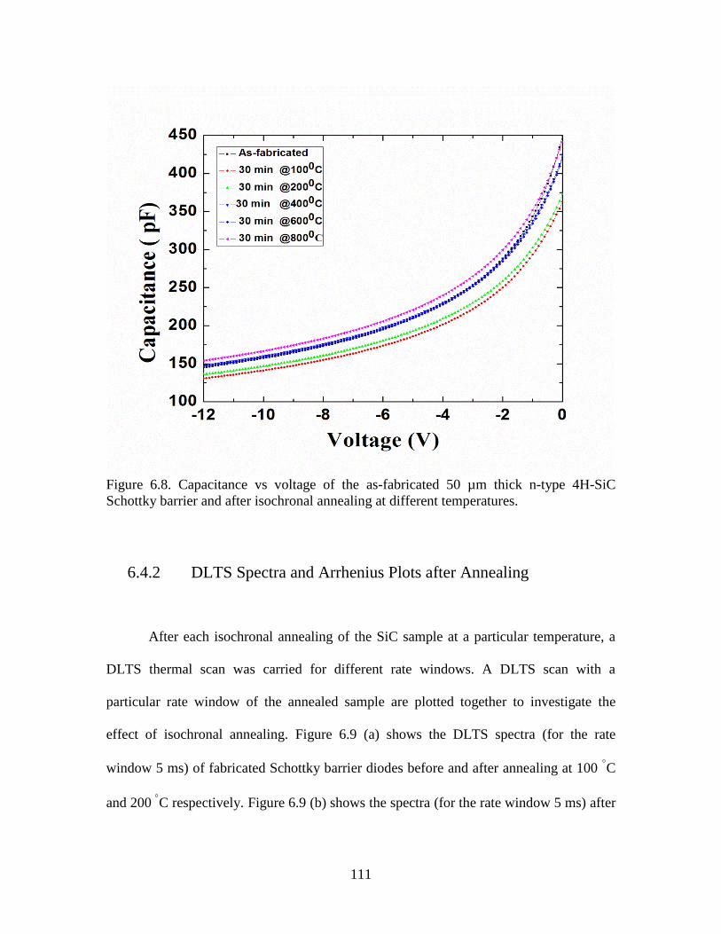
111
Figure 6.8. Capacitance vs voltage of the as-fabricated 50 µm thick n-type 4H-SiC
Schottky barrier and after isochronal annealing at different temperatures.
6.4.2 DLTS Spectra and Arrhenius Plots after Annealing
After each isochronal annealing of the SiC sample at a particular temperature, a
DLTS thermal scan was carried for different rate windows. A DLTS scan with a
particular rate window of the annealed sample are plotted together to investigate the
effect of isochronal annealing. Figure 6.9 (a) shows the DLTS spectra (for the rate
window 5 ms) of fabricated Schottky barrier diodes before and after annealing at 100 C
and 200 C respectively. Figure 6.9 (b) shows the spectra (for the rate window 5 ms) after
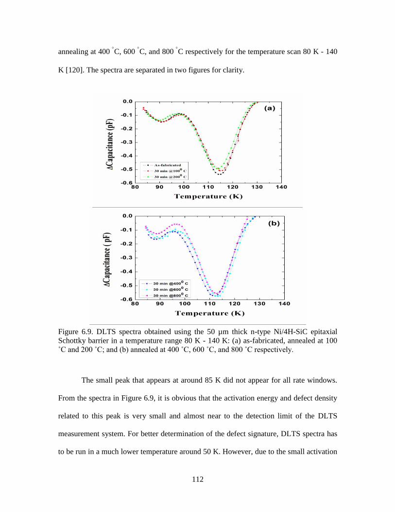
112
annealing at 400 C, 600
C, and 800
C respectively for the temperature scan 80 K - 140
K [120]. The spectra are separated in two figures for clarity.
Figure 6.9. DLTS spectra obtained using the 50 µm thick n-type Ni/4H-SiC epitaxial
Schottky barrier in a temperature range 80 K - 140 K: (a) as-fabricated, annealed at 100
˚C and 200 ˚C; and (b) annealed at 400 ˚C, 600 ˚C, and 800 ˚C respectively.
The small peak that appears at around 85 K did not appear for all rate windows.
From the spectra in Figure 6.9, it is obvious that the activation energy and defect density
related to this peak is very small and almost near to the detection limit of the DLTS
measurement system. For better determination of the defect signature, DLTS spectra has
to be run in a much lower temperature around 50 K. However, due to the small activation
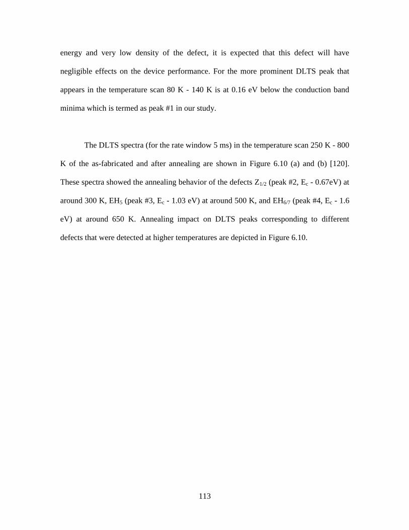
113
energy and very low density of the defect, it is expected that this defect will have
negligible effects on the device performance. For the more prominent DLTS peak that
appears in the temperature scan 80 K - 140 K is at 0.16 eV below the conduction band
minima which is termed as peak #1 in our study.
The DLTS spectra (for the rate window 5 ms) in the temperature scan 250 K - 800
K of the as-fabricated and after annealing are shown in Figure 6.10 (a) and (b) [120].
These spectra showed the annealing behavior of the defects Z1/2 (peak #2, Ec - 0.67eV) at
around 300 K, EH5 (peak #3, Ec - 1.03 eV) at around 500 K, and EH6/7 (peak #4, Ec - 1.6
eV) at around 650 K. Annealing impact on DLTS peaks corresponding to different
defects that were detected at higher temperatures are depicted in Figure 6.10.
114
Figure 6.10. DLTS spectra obtained in a temperature range 250 K - 750 K: (a) as-
fabricated and annealed at 100 ˚C and 200 ˚C; and (b) annealed at 400 ˚C, 600 ˚C, and
800 ˚C.
After isochronal annealing at different temperatures, an Arrhenius plot was drawn
from the peak temperatures in the DLTS spectra of the annealed sample. The defects
parameters for every individual defects are calculated from these Arrhenius plot. The
Arrhenius plot drawn after annealing at temperature 100 ˚C, 200 ˚C, 400 ˚C, 600 ˚C and
800 ˚C are shown in Figure 6.11, Figure 6.12, Figure 6.13, Figure 6.14, and Figure 6.15
respectively. The calculated defects parameters after annealing at temperatures 100 ˚C,

115
200 ˚C, 400 ˚C, 600 ˚C, and 800 ˚C are shown in Table 6.2, Table 6.3, Table 6.4, Table
6.5, and Table 6.6 respectively.
1 2 3 9 10 11 12
100
101
102
103
104
105 Peak #1
Peak #2
Peak #3
Peak #4
T
2 /en
(k2 S
)
103 / Temperature (1/K)
Figure 6.11. Arrhenius plot corresponding to the DLTS spectra obtained after annealing
at 100 ˚C.
Table 6.2. Defect parameters obtained after annealing at 100 ˚C
Peak # σn
cm2
E
eV
Nt
cm-3
Possible
Trap Identity
Peak 1 3.32× 10⁻¹⁵
Ec ˗ 0.17 1.13× 10¹³
Ti(c)
Peak 2 2.09× 10⁻¹⁵
Ec ˗ 0.65 6.38× 10¹²
Z1/2
Peak 3 1.61× 10⁻¹⁵
Ec ˗ 1.00 6.49× 10¹²
EH5
Peak 4 3.23× 10⁻¹⁵
Ec ˗ 1.70 6.38× 10¹²
EH6/7

116
Figure 6.12. Arrhenius plots corresponding to the DLTS spectra obtained after annealing
at 200 ˚C.
Table 6.3. Defect parameters after annealing at 200 ˚C
Peak # σn
cm2
ΔE
eV
Nt
cm-3
Possible
Trap Identity
Peak 1 2.18× 10⁻¹⁵
Ec ˗ 0.17 1.04× 10¹³
Ti (c)
Peak 2 4.27× 10⁻¹⁶
Ec ˗ 0.61 5.58× 10¹²
Z1/2
Peak 3 9.1× 10⁻¹⁶
Ec ˗ 1.14 5.71× 10¹²
EH5
Peak 4 6.66× 10⁻¹⁴
Ec ˗ 1.69 5.59× 10¹²
EH6/7

117
Figure 6.13. Arrhenius plots corresponding to the DLTS spectra obtained after annealing
at 400 ˚C
Table 6.4. Defect parameters after annealing at 400 ˚C
Peak # σn
cm2
E
eV
Nt
cm-3
Possible
Trap Identity
Peak 1 9.63× 10⁻¹⁶
Ec ˗ 0.15 1.17× 10¹³
Ti(c)
Peak 2 2.01× 10⁻¹⁶
Ec ˗ 0.60 7.19× 10¹²
Z1/2
Peak 3 6.02× 10⁻¹⁶
Ec ˗ 0.96 7.01× 10¹²
EH5
Peak 4 6.46× 10⁻¹⁴
Ec ˗ 1.71 7.44× 10¹²
EH6/7

118
Figure 6.14. Arrhenius plots corresponding to the DLTS spectra obtained after annealing
at 600 ˚C.
Table 6.5. Defect parameters after annealing at 600 ˚C
Peak # σn
cm2
E
eV
Nt
cm-3
Possible
Trap Identity
Peak 1 6.7× 10⁻¹⁶
Ec ˗ 0.14 1.23× 10¹³
Ti(c)
Peak 2 1.58× 10⁻¹⁶
Ec ˗ 0.60 8.06× 10¹²
Z1/2
Peak 3 3.71× 10⁻¹⁶
Ec ˗ 0.85 8.23× 10¹²
EH5
Peak 4 1.43× 10⁻¹⁴
Ec ˗ 1.34 3.32× 10¹²
EH6/7

119
Figure 6.15. Arrhenius plot corresponding to the DLTS spectra obtained after annealing
at 800 ˚C
Table 6.6. Defect parameters after obtained annealing 800 ˚C
Peak # σn
cm2
E
eV
Nt
cm-3
Possible
Trap Identity
Peak 1 6.28× 10⁻¹⁶
Ec ˗ 0.15 1.45× 10¹³
Ti(c)
Peak 2 2.28× 10⁻¹⁶
Ec ˗ 0.60 1.00× 10¹³
Z1/2
Peak 3 3.72× 10⁻¹⁶
Ec ˗ 1.14 9.56× 10¹²
EH5
Peak 4 2.23× 10⁻¹⁷
Ec ˗ 1.245 6.14× 10¹²
EH6/7

120
6.4.3 Analysis of the Impact of Annealing on Defects Parameters
To observe the effect of annealing, the defect parameters (capture cross section
and density) variation with annealing temperature are plotted for every individual defects.
For the peak # 1 which identified as Ti (c), the activation energy after annealing at
different temperatures up to 800 C lies within Ec - 0.16 ± 0.015 eV which means the
nature of the defect did not change much with annealing. The capture cross section and
defect density related to peak #1 are shown in Figure 6.16 (a) and Figure 6.16 (b),
respectively. The capture cross-section of the defect Ti (c) decreased up to the annealing
temperature of 400 C and remains unchanged for the annealing at higher temperatures.
On the other hand the defect density decreased with the annealing temperature up to 200
C and again increased gradually with the annealing temperature of 800 C, which is the
extent of our present studies.

121
Figure 6.16. Defect (Ec - 0.17 eV corresponding to peak #1) parameters variation with
annealing temperature: (a) capture cross-section, and (b) defect density.
Defect parameters variation of most prominent defect Z1/2 of 4H-SiC is located at
Ec - 0.67 eV is shown in Figure 6.17 [120]. The capture cross-section is decreased by
almost an order of magnitude through annealing up to 200 C and remains unchanged till
800 C. The defect density increased with the increase of annealing temperature after
showing an initial small decrease up to 200 C. This small decrease may be due to
migration or out-diffusion of carbon interstitial Ci. After 200 C, dopant nitrogen atoms
occupy the position of carbon atom which produces Ci resulting in an increase of Z1/2.
Eberlein et al. [121] has shown that the formation of Z1/2 is possible through the
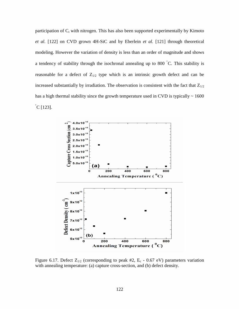
122
participation of Ci with nitrogen. This has also been supported experimentally by Kimoto
et al. [122] on CVD grown 4H-SiC and by Eberlein et al. [121] through theoretical
modeling. However the variation of density is less than an order of magnitude and shows
a tendency of stability through the isochronal annealing up to 800 C. This stability is
reasonable for a defect of Z1/2 type which is an intrinsic growth defect and can be
increased substantially by irradiation. The observation is consistent with the fact that Z1/2
has a high thermal stability since the growth temperature used in CVD is typically ~ 1600
C [123].
Figure 6.17. Defect Z1/2 (corresponding to peak #2, Ec - 0.67 eV) parameters variation
with annealing temperature: (a) capture cross-section, and (b) defect density.

123
The variation of capture cross-section and defect density of EH5 is shown in
Figure 6.18. The capture cross-section of the defect is decreased slightly and remains
unchanged throughout our annealing study. Annealing impact on the defect density of
EH5 showed a decrease up to 200 C and increases with annealing temperature. Negoro et
al. [124] identified a similar defect at 0.95 ± 0.05 eV as RD1/2 and showed that the defect
density increases slightly with the increase of annealing temperature. On the other hand,
Alfieri et al. [123] showed that the defect density located at Ec - 1.03 eV is slightly
decreased with the annealing up to the temperature 600 C and the defect density goes
below the detection limit after annealing at 1300 C. In our studies we found similar
annealing response of defect density for Z1/2 and EH5. This is due to the same origin of
formation of these two defects related to the displacement of carbon from the lattice
structure. Z1/2 is thought to be formed due to carbon interstitials, and EH5 is thought to be
formed due to carbon clustering. Hemmingsson et al. [95] observed EH5 defect in the
samples with a 2.5 MeV electron irradiation for doses higher than 1014
cm-2
. But Storasta
et al. [104] did not see this defect when the samples were exposed in low energy
irradiation (250 keV) which is close to the threshold for atomic displacement of carbon.
This also suggests EH5 is related to carbon cluster defects.

124
Figure 6.18. Defect EH5 (corresponding to peak #3, Ec - 1.03 eV) parameters variation
with annealing temperature: (a) capture cross-section, and (b) defect density.
In our studies the variation of capture cross-sections and densities of EH6/7 defect
with isochronal annealing do not follow any trend as shown in Figure 6.19. Though the
variation of defects parameters is random but the range of variation is very small, which
suggests the defect is very stable up to a temperature of 800 C. Several groups have
shown that the defect EH6/7 is very stable up to a temperature of 1000 C [123, 124, 105].

125
Figure 6.19. Defect EH6/7 (corresponding to peak #4, Ec - 1.6 eV) parameters variation
with annealing temperature: (a) capture cross-section, and (b) defect density.
6.5 CONCLUSION
Isochronal annealing studies are carried out in the temperature range from 100 ˚C
to 800 ˚C on 50 μm n-type 4H-SiC epitaxial layers. Defect levels have been investigated
and characterized thoroughly on as-fabricated and isochronal annealed Schottky diodes

126
through deep level transient spectroscopy. Four different defect levels located at Ec - 0.17
eV, Ec - 0.67 eV, Ec - 1.03 eV, and Ec - 1.6 eV are identified as Ti (c), Z1/2, EH5, and
EH6/7, respectively. The capture cross-section of the shallow defect level Ec ˗ 0.17 eV for
Ti (c) was reduced with increasing annealing temperature while the defect density was
not changed significantly. Similar annealing behavior of Z1/2 and EH5 were correlated
very well with these defect levels having the same origin of formation. Z1/2 is related to
carbon interstitial, and EH5 is related to carbon cluster. The defect parameters of EH6/7
changed randomly within a small range up to the upper annealing temperature range of
800 ˚C. The most common two intrinsic deep level defects Z1/2 and EH6/7 were found to
be stable up to the limit of our experiment of 800 ˚C.

127
CHAPTER 7: CONCLUSION AND SUGGESTIONS FOR FUTURE
WORK
7.1 CONCLUSION
This dissertation is focused on the investigation the deep level defects of 4H-SiC
epitaxial layers. A comprehensive study on the fabrication and characterization of 4H-
SiC radiation detector has been performed. The characterization techniques are based on
electrical measurements which include current - voltage and capacitance - voltage studies
to know electrical behavior of the devices, spectroscopic measurements to see the alpha
response, DLTS measurements to detect deep level defects, and isochronal annealing to
observe the impact of annealing on defects.
Radiation detectors based on Schottky diodes are fabricated on high quality 20
µm and 50 µm thick n-type 4H-SiC epitaxial layers. The epitaxial layers were grown by
chemical vapor deposition on 4H-SiC (0001) n-type substrates. The properties of the
fabricated Schottky barriers are determined by current-voltage (I-V) and capacitance-
voltage (C-V) measurements. The high barrier height (of the order of 1.6 eV, was
calculated by using a thermionic emission model) of the Schottky devices offered very
low leakage current (of the order of few pA) at the reverse bias of ~-100 V. Due to this
good Schottky behavior and low leakage current, the fabricated detectors are found to be
128
very suitable for radiation detectors. Alpha spectroscopic measurements of the fabricated
detectors are performed by using a 241
Am radiation source and the percentage energy
resolution of the detectors was found to be in the range of 0.29 % - 1.8 % for 5486 keV
alpha particle peak.
Deep level transient spectroscopy (DLTS) studies were conducted in the
temperature range of 80 K - 800 K to investigate the deep level defects. Types of
identified defects and defect parameters are varied widely from the detector to detector.
In all of the detectors fabricated on 20 µm thick epitaxial layers, deep level defects Z1/2
located at Ec - 0.6 eV, Ci1 located at Ec - 1.3 eV, and EH6/7 located at Ec - 1.6 eV are
found by the DLTS measurements. Among them two defect levels (electron traps) Z1/2
and EH6/7 which are related to carbon vacancies and their complexes mostly affected the
detector resolution. Defect level observed at Ec - 1.3 eV is found not to affect the
detectors performance. For the case of 50 µm epitaxial layer the detected defects are
identified as Ti(c) at Ec – 0.13 eV, Ti (c) at Ec – 0.17 eV, Z1/2 at Ec - 0.67 eV, EH5 at Ec -
1.04 eV, Ci1 at Ec - 1.3 eV, and a newly detected deep level at Ec - 2.4 eV. Deep level
defect located at Ec - 2.4 eV is identified for the first time. Along with Z1/2 and EH5, the
newly identified defect at Ec - 2.4 eV mostly affected the detector resolution fabricated on
50 µm 4H-SiC epitaxial layers.
To investigate the annealing behavior of deep level defects, isochronal annealing
studies were carried out in the temperature range 100 ˚C to 800 ˚C on 50 μm n-type 4H-
SiC epitaxial layers. Four different defects Ti (c) located at Ec - 0.17 eV, Z1/2 located at Ec
129
- 0.67 eV, EH5 located at Ec - 1.03 eV, and EH6/7 located at Ec - 1.6 eV are responded
differently to the annealing studies. Capture cross sections and densities of every
individual defects are plotted to see the impact of annealing. The capture cross-section of
the shallow defect level Ec ˗ 0.17 eV for Ti (c) was reduced with increasing annealing
temperature while the defect density was not changed significantly. Similar annealing
behavior of Z1/2 and EH5 were correlated very well with the understanding of these defect
levels having the same origin of formation. Z1/2 is related to carbon interstitial, and EH5 is
related to carbon cluster. The defect parameters of EH6/7 changed randomly within a
small range up to the upper annealing temperature range of 800 ˚C in this study. The
most common two intrinsic deep level defects Z1/2 and EH6/7 were found to be stable up
to the limit of our experiment of 800 ˚C.
7.2 FUTURE WORK
Due to high band-gap and good crystallinity, 4H-SiC epitaxial layer is an
excellent material for fabrication of alpha particle detectors. The resolutions of Schottky
barrier based detectors are found to be limited by the deep level defects present within the
4H-SiC epitaxial layers. To improve the detector performance and minimize the defects’
role, the following suggestions for future research work have emerged from the present
investigations:
Surface passivation prior to detector fabrication can be applied to improve
the radiation detector performance. It is likely that both the reverse

130
leakage current and energy resolution can be improved by eliminating
surface and interface states through passivation. Dielectric layer grown by
PECVD or MOCVD such as silicon dioxide (SiO2), silicon nitride (Si3N4),
and Si-O-N are the most suitable materials for passivation.
In this work nickel is used for Schottky barrier fabrication. Detector
fabrication with high work function metals such as ruthenium, palladium,
and platinum may improve the Schottky barrier properties. It is expected
that these high work function metals will reduce the leakage current and
will minimize the deep level effects to hence improve the detector
performance.
After delineating the microscopic defects on the epitaxial layers, the
Schottky barrier based devices can be fabricated on different location on
the epitaxial surfaces. Correlation of the deep level defects with
microscopic defects can be carried out through DLTS measurements on
the Schottky devices fabricated in the region with microscopic defect and
in the defect free region.
Various thicknesses (other than 20 µm and 50 µm) of 4H-SiC epitaxial
layers can be used to fabricate the Schottky barrier to see the improvement
on detector resolution. DLTS measurements can be used to investigate the

131
deep centers in different thick epitaxial layers and the impact of deep
centers on the high energy detector performance.
Detailed theoretical studies by DFT (Density Functional Theory) and ab-
initio calculations may be interesting to investigate the microstructure of
newly identified deep level defects located far below from the conduction
band (Ec - 2.4 eV).

132
REFERENCES
[1] S. T. Pantelides, "The electronic structure of impurities and other point defects in
semiconductors," Review of Modern Physics, vol. 50, no. 4, pp. 797-858, 1978.
[2] K. C. Mandal, S. K. Chaudhuri, K. V. Nguyen and M. A. Mannan, "Correlation of
Deep Levels With Detector Performance in 4H-SiC Epitaxial Schottky Barrier
Alpha Detectors," IEEE Transaction on Nuclear Science, vol. 61, no. 4, pp. 2338-
2344, 2014.
[3] A. Rohatgi, R. H. Hopkins, J. R. Davis, R. B. Cambell and H. C. Mollenkopf, "The
impact of molybdenum on silicon and silicon solar cell performance," Solid State
Electronics, vol. 23, no. 11, pp. 1185-1190, 1981.
[4] M. Jaros and S. Brand, "Localized defects in III-V semiconductors," Physical
Review B, vol. 14, no. 10, pp. 4494-4505, 1976.
[5] G. A. Baraff, E. O. Kane and M. Schluter, "Silicon Vacancy: A Possible "Anderson
Negative-U” System," Physical Review Letters, vol. 43, no. 13, pp. 956-959, 1979.
[6] E. O. Kane and M. Schluter, "Charge disturbances around neutral defects: A simple
new method applied to the ideal silicon vacancy," Physical Review B, vol. 19, no.
10, pp. 5232-5239, 1979.
[7] T. Shimizu and K. Minami, "LCAO MO treatment for the S+ donor in Si," Physica
Status Solidi (b), vol. 48, no. 2, pp. K181-K184, 1971.
[8] I. Gorczyca, A. Svane and N. E. Christensen, "Theoretical study of point defects in
GaN and AlN; lattice relaxations and pressure effects," MRS Internet Journal of
Nitride Semiconductor Research, vol. 2, p. e18, 1997.
[9] R. Williams, "Criterion for Continuous Amplitude Oscillations of Optical Masers,"
Journal of Applied Physics, vol. 37, no. 9, pp. 3411-3412, 1966.
[10] L. Forbes and C. T. Sah, "On the determination of deep level center energy and
concentration by thermally stimulated conductivity measurements using reverse-
biasedp-njunctions," Solid-State Electronics, vol. 14, no. 2, pp. 182-183, 1971.
[11] C. T. Sah, W. Chan, H. Fu and J. W. Walker, "Thermally Stimulated Capacitance
(TSCAP) in p-n Junctions," Applied Physics Letters, vol. 20, no. 5, pp. 193-195,
1972.
[12] C. T. Sah, L. Forbes, L. L. Rosier and A. F. Tasch, "Thermal and optical emission
and capture rates and cross sections of electrons and holes at imperfection centers
in semiconductors from photo and dark junction current and capacitance
experiments," Solid State Electronics, vol. 13, no. 6, pp. 759-788, 1970.
[13] C. T. Sah, "Bulk and interface imperfections in semiconductors," Solid State
Electronics, vol. 19, no. 12, pp. 975-990, 1976.
[14] D. V. Lang, "Deep‐level transient spectroscopy: A new method to characterize
traps in semiconductors," Journal of Applied Physics, vol. 45, no. 7, pp. 3023-3032,
1974.
[15] J. K. Rhee and T. Ikoma, "Photoinduced current transient spectroscopy of semi-
insulating InP:Fe and InP:Cr," Journal of Applied Physics, vol. 53, no. 6, pp. 4247-
4249, 1982.
[16] R. E. Kremer, M. Arikan, J. C. Abele and J. Blakemore, "Transient
photoconductivity measurements in semi-insulating GaAs. I. An analog approach,"
Journal of Applied Physics, vol. 62, no. 6, pp. 2424-2431, 1987.
[17] J. A. PALS, "Properties of Au, Pt, Pd and Rh levels in silicon measured with a
constant capacitance technique," Solid State Electronics, vol. 17, no. 11, pp. 1139-
1145, 1974.
[18] INSPEC, Properties of Gallium Arsenide, London: The Institution of Electrical
Engineers, 1986.
[19] Z. Q. Fang, D. C. Look, W. Kim, Z. Fan, A. Botchkarev and H. Morkoc, "Deep
centers in n-GaN grown by reactive molecular beam epitaxy," Applied Physics
Letters, vol. 72, no. 18, pp. 2277-2279, 1998.
[20] Z. Q. Fang, D. C. Look, J. Jasinski, M. Benamara, Z. Liliental-Weber and R. J.
Molnar, "Evolution of deep centers in GaN grown by hydride vapor phase epitaxy,"
Applied Physics Letters, vol. 78, no. 3, pp. 332-334, 2001.
[21] F. Riedel and W. Schroter, "Electrical and structural properties of nanoscale NiSi2
precipitates in silicon," Physical Review B, vol. 62, no. 11, pp. 7150-7156, 2000.
[22] S. Das, S. K. Chaudhuri, R. N. Bhattacharya and K. C. Mandal, "Defect levels in
Cu2ZnSn(SxSe1-x)4 solar cells probed by current-mode deep level transient
spectroscopy," Applied Physics Letters, vol. 104, no. 19, pp. 192106(1-4), 2014.
[23] M. Igalson, P. Zabierowski, A. Romeo and L. Stolt, "Reverse –bias DLTS for
investigation of the interface region of thin film solar cells," Opto-Electronics
Review, vol. 8, no. 4, p. 346 –349, 2000.
[24] S. F. Yoon, K. H. Yip, H. Q. Zheng and B. P. Gay, "Effect of deep levels on the
characteristics of InGa1-xP/In0.20Ga0.80As/GaAs high-electron mobility transistor
grown by solid-source MBE," Journal of Crystal Growth, vol. 217, no. 1-2, pp. 33-
39, 2000.
[25] V. W. Ilchenko, S. D. Lin, C. P. Lee and O. V. Tretyak, "Deep level transient
spectroscopy characterization of InAs self-assembled quantum dots," Journal of
Applied Physics, vol. 89, no. 2, pp. 1172-1174, 2001.
[26] R. Magno, B. R. Bennett and E. R. Glaser, "Deep level transient capacitance
measurements of GaSb self-assembled quantum dots," Journal of Applied Physics,
vol. 88, no. 10, pp. 5843-5849, 2000.
[27] J. J. Berzelius, "Untersuchungen über die Flussspathsäure und deren
merkwürdigsten Verbindungen," Annalen der Physik, vol. 77, no. 6, pp. 169-230,
1824.
[28] L. S. Ramsdell, "Studies on silicon carbide," American Mineralogist, vol. 32, pp.
64-82, 1947.
[29] T. Kinoshita, K. M. Itoh, J. Muto, M. Schadt, G. Pensl and K. Takeda, "Calculation

of the Anisotropy of the Hall Mobility in N-type 4H- and 6H-SiC," Material
Science Forum, vol. 264–268, pp. 295-298, 1998.
[30] W. J. Choyke, H. Matsunami and G. Pensi, Silicon Carbide: A Review of
Fundamental Questions and Applications to Current Device Technology, Berlin:
Wiley-VCH, 1997.
[31] G. L. Harris, Properties of SiC, London: INSPEC, 1995.
[32] B. Ellis and T. S. Moss, "The Conduction bands in 6H and 15R silicon carbide,
Hall effect and infrared Faraday rotation measurements," in Proceeding of the
Royal Society of London, London, 1967.
[33] G. A. Lomakina, "Silicon carbide Proceeding," in 3 rd International Confernce on
Silicon Carbide, Miami, 1973.
[34] S. Karmann, W. Suttrop, A. Schoner, M. Schadt, C. Haberstroh, F. Engeibrecht, R.
Helbig, G. Penal, R. A. Stein and S. Leibenzeder, "Chemical vapor deposition and
characterization of undoped and nitrogen‐doped single crystalline 6H‐SiC,"
Journal of Applied Physics, vol. 72, no. 11, pp. 5437-5442, 1992.
[35] F. Nava, G. Bertuccio, A. Cavallini and E. Vittone, "Silicon carbide and its use as a
radiation detector material," Measurement Science and Technology, vol. 19, pp.
102001(1-25), 2008.
[36] Y. M. Tairov and V. F. Tsvetkov, "General principles of growing large-size single
crystals of various silicon carbide polytypes," Journal of Crystal Growth, vol. 52,
no. 1, pp. 146-150, 1981.
[37] S. G. Muller, R. C. Glass, H. M. Hobgood, V. F. Tsvetkov, M. Brady, D. Henshall,
J. R. Jenny, D. Malta and C. H. Carter, "The status of SiC bulk growth from an
industrial point of view," Journal of Crystal Growth, vol. 211, no. 1-4, pp. 325-
332, 2000.
[38] J. J. Sumakeris, J. R. Jenny and A. R. Powell, "Bulk crystal growth, epitaxy, and
defect reduction in silicon carbide materials for microwave and power devices,"
MRS Bulletin, vol. 30, no. 4, pp. 280-286, 2005.
[39] CREE, "Cree Silicon Carbide Substrates and Epitaxy," CREE, March 2015.
[Online]. Available: http://www.cree.com/LED-Chips-and-Materials/Materials.
[40] S. V. Rendakova, I. P. Nikitina, A. S. Tregubova and V. A. Dmitriev, "Micropipes
and dislocation density reduction in 6H-SiC and 4H-SiC Structure grown by liquid
phase epitaxy," Journal of Electronic Materials, vol. 27, pp. 292-295, 1998.
[41] A. R. Powell and L. B. Rowland, "SiC materials - Progress, status, and potential
roadblocks," Proceedings of the IEEE, vol. 90, no. 6, pp. 942-955, 2002.
[42] O. Kordina, C. Hallin, A. Henry, J. P. Bergman, I. G. Ivanov, A. Ellison, N. T. Son
and E. Janzen, "Growth of SiC by Hot-Wall CVD and HTCVD," Physica Status
Solidi (b), vol. 202, pp. 321-334, 1997.
[43] A. Owens and A. Peacock, "Compound semiconductor radiation detectors,"
Nuclear Instruments and Methods in Physics Research Section A: Accelerators,
Spectrometers, Detectors and Associated Equipment, vol. 531, no. 1-2, pp. 18-37,
2004.
[44] P. Blood and J. W. Orton, "The Electrical Characterization of Semiconductors:
Majority Carriers and Electron States," in Techniques of Physics, San Diego, 1992.
[45] S. M. Sze and K. K. Ng, Physics of Semiconductor devices, New Jersey: John
Wiley & Sons, 2007.
[46] E. H. Rhoderick and R. H. Williams, Metal-Semiconductor Contacts, New York:
Clarendon Press. Oxford, 1988.
[47] S. S. Li, Semiconductor Physical Electronics, New York: Springer, 2006.
[48] H. A. Bethe, "Theory of the Boundary Layer of Crystal Rectifiers," MIT Radiation
. Laboratory, Boston, 1942.
[49] D. K. Schroder, Semiconductor Material and Device Characterization, New York:
John Wiley & Sons, 1998.
[50] R. T. Tung, "Electron transport at metal-semiconductor interfaces: General theory,"
Physical Review B, vol. 45, no. 23, pp. 13509-13523, 1992.
[51] P. G. Muzykov, R. M. Krishna and K. C. Mandal, "Temperature dependence of
current conduction in semi-insulating 4H-SiC epitaxial layer," Applied Physics
Letters, vol. 100, no. 3, pp. 032101(1-4), 2012.
[52] D. A. Neamen, Semiconductor Physics andz Devices, Basic Principle, McGraw-
Hill, 2012.
[53] A. Hallen and M. Bakowski, "The influence of ion flux on defect production in
MeV proton-irradiated silicon," Solid-State Electronics, vol. 32, no. 11, pp. 1033-
1037, 1989.
[54] F. D. Auret and P. N. K. Deenapanray, "Deep Level Transient Spectroscopy of
Defects in HighEnergy Light-Particle Irradiated Si," Critical Review in Solid State
and Materials Sciences, vol. 29, no. 1, pp. 1-44, 2004.
[55] J. A. Powell and D. J. Larkin, "Process-Induced Morphological Defects in Epitaxial
CVD Silicon Carbide," Physics Status Solidi (b), vol. 202, no. 1, pp. 529-548,
1997.
[56] T. Kimoto, N. Miyamoto and H. Matsunami, "Performance Limiting Surface
Defects in SiC Epitaxial p-n Junction Diodes," IEEE Transaction on Electron
Devices, vol. 46, no. 3, pp. 471-477, 1999.
[57] Cree Incorporated, "SiC data Sheets," Cree Research Incorporation, Durham, NC,
1999.
[58] T. Kuhr, E. Sanchez, M. Skowronski, W. Vetter and M. Dudley, "Hexagonal voids
and the formation of micropipes during SiC sublimation growth," Journal of
Applied Physics, vol. 89, no. 8, pp. 4625-4630, 2001.
[59] E. Sanchez, S. Ha, J. Grim, M. Skowronski, W. Vetter, M. Dudley, R. Bertke and
W. Mitchel, "Assessment of Polishing-Related Surface Damage in Silicon
Carbide," Journal of Electrochemical Society, vol. 149, no. 2, pp. G131-G136,
2002.
[60] P. G. Neudeck and J. A. Powell, "Performance limiting micropipe defects in silicon
carbide wafers," IEEE Electron Devices Letters, vol. 15, no. 2, pp. 63-65, 1994.
[61] U. Zimmermann, A. Hallen, A.O.Konstantinov and B. Breitholtz, "Investigations
of microplasma breakdown in 4H silicon carbide," in Materials Research Society
Symposium Proceeding, San Francisco, California, 1998.

[62] M. Dudley, S. Wang, W. Huang, C. H. Carter, V. F. Tsvetkov and C. Fazi, "White-
beam synchrotron topographic studies of defects in 6H-SiC single crystals,"
Journal of Physics D: Applied Physics, vol. 28, no. 4A, pp. A63-A68, 1995.
[63] P. G. Neudeck, "Electrical Impact of SiC Structural Defects on High Electric Field
Devices," Materials Science Forum, Vols. 338-342, pp. 1161-1166, 2000.
[64] P. G. Neudeck, W. Huang and M. Dudley, "Study of Bulk and Elementary Screw
Dislocation Assisted Reverse Breakdown in Low-Voltage (< 250 V) 4H–SiC p+ n
Junction Diodes—Part I: DC Properties," IEEE Transaction of Electron Devices,
vol. 46, no. 3, pp. 478-484, 1999.
[65] Q. Wahab, A. Ellison, A. Henry, E. Janzen, C. Hallin, J. D. Persio and R. Martinez,
"Influence of epitaxial growth and substrate-induced defects on the breakdown of
4H–SiC Schottky diodes," Applied Physics Letters, vol. 76, no. 19, pp. 2725-2727,
2000.
[66] H. Lendenmann, F. Dahlquist, N. Johansson, R. Soderholm, P. A. Nilsson, J. P.
Bergman and P. Skytt, "Long term operation of 4.5kV PiN and 2.5kV JBS diodes,"
Material Science Forum, Vols. 353-356, pp. 727-730, 2001.
[67] S. Ha, M. Skowronski, W. M. Vetter and M. Dudley, "Basal plane slip and
formation of mixed-tilt boundaries in sublimation grown hexagonal polytype
silicon carbide single crystals," Journal of Applied Physics, vol. 92, no. 2, pp. 778-
785, 2002.
[68] J. Fan and P. K. Chu, Silicon Carbide Nanostructures: Fabrication, Structure, and
Properties, Springer, 2014.
[69] S. Ha, N. T. Nufher, G. S. Rohrer, M. D. Graef and M. Skowronski, "Identification
of Prismatic Slip Bands in 4H SiC Boules Grown by Physical Vapor Transport,"
Journal of Electronic Materials, vol. 29, no. 7, pp. L5-L8, 2000.
[70] S. Ha, W. M. Vetter, M. Dudley and M. Skowronski, "A simple mapping method
for elementary dislocations in heteroepitaxial SiC layers," Material Science Forum,
vol. 389–393, pp. 443-446, 2002.
[71] S. Amelinckx and G. Strumane, "Dislocations in Silicon Carbide," Journal of
Applied Physics, vol. 31, no. 8, pp. 1359-1370, 1960.
[72] E. K. Sanchez, J. Q. Liu, M. D. Graef, M. Skowronski, W. M. Vetter and M.
Dudley, "Nucleation of threading dislocations in sublimation grown silicon
carbide," Journal of Applied Physics, vol. 91, no. 3, pp. 1143-1148, 2002.
[73] J. Takahashi, M. Kanaya and Y. Fujiwara, "Sublimation growth of SiC single
crystalline ingots on faces perpendicular to the (0001) basal plane," Journal of
Crystal Growth, vol. 135, no. 1-2, pp. 61-70, 1994.
[74] D. Siche, D. Klimm, T. Hölzel and A. Wohlfart, "Reproducible defect etching of
SiC single crystals," Journal of Crystal Growth, vol. 270, no. 1-2, pp. 1-6, 2004.
[75] M. A. Mannan, S. K. Chowdhuri, K. V. Nguyen and K. C. Mandal, "Effect of Z1/2 ,
EH5 and Ci1 deep defects on the perormance of n-type 4H-SiC epitaxial layers
Schottky detectors : Alpha spectroscopy and deep level transient spectroscopy
studies," Journal of Applied Physics, vol. 115, no. 22, pp. 224504 (1-6), 2014.
[76] M. E. Levinshtein, S. L. Rumyantsev and M. S. Shur, Properties of Advanced

Semiconductor Materials: GaN, AlN, InN, BN, SiC, SiGe, London: John Wiley &
Sons, 2001.
[77] M. Jang, Y. Kim, J. Shin and S. Lee, "Characterization of erbium-silicided
Schottky diode junction," IEEE Electron Devices Letter, vol. 26, no. 6, p. 354 –
356, 2005.
[78] G. F. Knoll, Radiation Detection and Measurement, New York: John Wiley &
Sons, 2000.
[79] M. B. H. Breese, "A theory of ion beam induced charge collection," Journal of
Applied Physics, vol. 74, no. 6, pp. 3789-3799, 1993.
[80] J. F. Ziegler, J. Biersack and U. Littmark, The Stopping and Range of Ions in
Matter, New York: Pergamon Press, 1985.
[81] S. N. Ahmed, Physics & Engineering of Radiation Detection, San Diego: Elsevier,
2007.
[82] A. Owens and A. Peacock, "Compound semiconductor radiation detectors,"
Nuclear Instruments and Methods in Physics Research, vol. 531, no. 1-2, pp. 18-
37, 2004.
[83] S. K. Chaudhuri, K. J. Zavalla and K. C. Mandal, "Experimental determination of
electron-hole pair creation energy in 4H-SiC epitaxial layer: An absolute
calibration approach," Applied Physics Letters, vol. 102, no. 3, pp. 031109 (1-4),
2013.
[84] Z.-Q. Fang, B. Claflin, D. C. Look, L. Polenta and W. C. Mitchel, "Thermally
stimulated current spectroscopy of high-purity semiinsulating 4H-SiC substrates,"
Journal of Electronic Materials, vol. 34, pp. 336-340, 2005.
[85] D.C. Look, "The Electrical and Photoelectronic Properties of Semi-Insulating
GaAs," Semiconductors and Semimetals, vol. 19, pp. 75-170, 1983.
[86] K. C. Mandal, P. G. Muzykov, R. Krishna, T. Hayes and T. S. Sudarshan,
"Thermally stimulated current and high temperature resistivity measurements of 4H
semi-insulating silicon carbide," Solid State Communications, vol. 151, no. 7, pp.
532-535, 2011.
[87] K. C. Mandal, R. Krishna, P. G. Muzykov, T. Hayes and T. S. Sudarshan,
"Characterization of Semi-Insulating 4H Silicon Carbide for Radiation Detectors,"
IEEE Transactions on Nuclear Science, vol. 58, pp. 1992-1999, 2011.
[88] M. Pavlovic and U. V. Desnica, "Precise determination of deep trap signatures and
their relative and absolute concentrations in semi-insulating GaAs," Journal of
Applied Physics, vol. 84, no. 4, pp. 2018-2024, 1998.
[89] A. A. Lebedev, "Deep level centers in Silicon Carbide," Semiconductors, vol. 19,
pp. 107-130, 1999.
[90] W. C. Mitchel, R. Perrin, J. Goldstein, A. Saxler, M. Roth, S. R. Smith, J. S.
Solomon and A. O. Evwaraye, "Fermi level control and deep levels in semi-
insulating 4H–SiC," Journal of Applied Physics, vol. 86, no. 9, pp. 5040-5044,
1999.
[91] J. R. Jenny, S. G. Müller, A. Powell, V. F. Tsvetkov, H. M. Hobgood, R. C. Glass
and C. H. Carter, "High-purity semi-insulating 4H-SiC grown by the seeded-
sublimation method," Journal of Electronic Materials, vol. 31, no. 5, pp. 366-369,
2002.
[92] K. C. Mandal, R. Krishna, P. G. Muzykov, S. K. Chowdhuri and J. R. Terry,
"Assessment of 4H-SiC epitaxial layers and high resistivity bulk crystals for
radiation detectors," in SPIE Conference, San Diego, 2012.
[93] P. G. Muzykov, R. M. Krishna and K. C. Mandal, "Characterization of deep levels
in n-type and semi-insulating 4H-SiC epitaxial layers by thermally stimulated
current spectroscopy," Journal of Applied Physics, vol. 111, no. 1, pp. 014910 (1-
7), 2012.
[94] L. Storasta, F. H. C. Carlsson, S. G. Sridhara, J. P. Bergman, A. Henry, T. Egilsson,
A. Hallén and E. Janzén, "Pseudodonor nature of the DI defect in 4H-SiC," Applied
Physics Letters, vol. 78, no. 1, pp. 46-48, 2001.
[95] C. Hemmingsson, N. T. Son, O. Kordina, J. P. Bergman, E. Janzén, J. L.
Lindstrӧm, S. Savage and N. Nordell, "Deep level defects in electron-irradiated 4H
SiC epitaxial layers," Journal of Applied Physics, vol. 81, no. 9, pp. 6155-6159,
1997.
[96] K. Danno and T. Kimoto, "Deep level transient spectroscopy on as-grown and
electron-irradiated p-type 4H-SiC epilayers," Journal of Applied Physics, vol. 101,
no. 10, pp. 103704(1-5), 2007.
[97] I. Pintilie, L. Pintilie, K. Irmsche and B. Thomas, "Deep levels in as-grown 4H-SiC
epitaxial layers and their correlation with CVD parameters," Material Science
Forum, Vols. 433-436, pp. 463-466, 2003.
[98] N. T. Son, B. Magnusson, Z. Zolnai, A. Ellison and E. Janzén, "Defects in High-
Purity Semi-Insulating SiC," Material Science Forum, Vols. 457-460, pp. 437-442,
2004.
[99] T. Dalibor and G. Pensl, "Electrical properties of the titanium acceptor in silicon
carbide," Physical Review B, vol. 55, no. 20, pp. 13618-13624, 1997.
[100] T. Dalibor, G. Pensl, H. Matsunami, T. Kimoto, W. J. Choyke, A. Schöner and N.
Nordell, "Deep defect centers in silicon carbide monitored with deep level transient
spectroscopy," Physica Status Solidi (a), vol. 162, no. 1, pp. 199-225, 1997.
[101] Ł. Gelczuk, M. D. browska-Szata, M. Sochacki and J. Szmidt, "Characterization of
deep electron traps in 4H-SiC Junction Barrier Schottky rectifiers," Solid-State
Electronics, vol. 94, pp. 56-60, 2014.
[102] J. Zhang, L. Storasta, J. P. Bergman, N. T. Son and E. Janzén, "Electrically active
defects in n-type 4H–silicon carbide grown in a vertical hot-wall reactor," Journal
of Applied Physics, vol. 93, no. 8, pp. 4708-4714, 2003.
[103] A. Castaldini, A. Cavallini, L. Polenta, F. Nava, C. Canali and C. Lanzieri,
"Defective states analysis in Silicon Carbide," Applied Surface Science, vol. 187,
no. 3, pp. 248-252, 2002.
[104] L. Storasta, J. P. Bergman, E. Janzen, A. Henry and J. Lu, "Deep levels created by
low energy electron irradiation in 4H-SiC," Journal Applied Physics, vol. 96, no. 9,
pp. 4909-4915, 2004.
[105] K. Danno and T. Kimoto, "Investigation of deep levels in n-type 4H-SiC epilayers
irradiated with low-energy electrons," Journal of Applied Physics, vol. 100, no. 11,
pp. 113728(1-6), 2006.
[106] T. Hornos, A. Gali and B. G. Svensson, "Large-Scale Electronic Structure
Calculations of Vacancies in 4H-SiC Using the Heyd-Scuseria-Ernzerhof Screened
Hybrid Density Functional," Material Science Forum, Vols. 679 - 680, pp. 261-
264, 2011.
[107] N. Iwamoto, B. C. Johnson, N. Hoshino, M. Ito, H. Tsuchida, K. Kojima and T.
Ohshima, "Defect-induced performance degradation of 4H-SiC Schottky barrier
diode particle detectors," Journal of Applied Physics, vol. 113, no. 14, pp.
143714(1-5), 2013.
[108] F. Nava, A. Castaldini, A. Cavallini, P. Errani and V. Cindro, "Radiation Detection
Properties of 4H-SiC Schottky Diodes Irradiated Up to 1016 n/cm2 by 1 MeV
Neutrons," IEEE Transaction of Nuclear Science, vol. 53, no. 5, pp. 2977-2982,
2006.
[109] A. Kawasuso, F. Redmann, R. Krause-Rehberg, P. Sperr, T. Frank, M. Weidner, G.
Pensl and H. Itoh, "Annealing process of defects in epitaxial SiC induced by He
and electron irradiation: Positron annihilation study," Material Science Forum,
Vols. 353-356, pp. 537-540, 2001.
[110] T. A. G. Eberlein, C. J. Fall, R. Jones, P. R. Briddon and S. Öberg, "Alphabet
luminescence lines in 4H−SiC," Physical Review B, vol. 65, pp. 184108(1-4), 2002.
[111] T. Tawara, H. Tsuchida, S. Izumi, I. Kamata and K. Izumi, "Evaluation of Free
Carrier Lifetime and Deep Levels of the Thick 4H-SiC Epilayers," Materials
Science Forum, Vols. 457-460, pp. 565-568, 2004.
[112] P. B. Klein, B. V. Shanabrook, S. W. Huh, A. Y. Polyakov, M. Skowronski, J.
Sumakeri and M. J. O’Loughlin, "Lifetime-limiting defects in n- 4H-SiC
epilayers," Applied Physics Letters, vol. 88, no. 5, pp. 052110(1-3), 2006.
[113] T. Kimoto, K. Danno and J. Suda, "Lifetime-killing defects in 4H-SiC epilayers
and lifetime control by low-energy electron irradiation," Physica Status Solidi (b),
vol. 245, no. 7, pp. 1327-1336, 2008.
[114] G. Alfieri and T. Kimoto, "Capacitance spectroscopy study of deep levels in Cl-
implanted 4H-SiC," Journal of Applied Physics, vol. 112, no. 6, pp. 063717(1-4),
2012.
[115] F. C. Beyer, C. G. Hemmingsson, H. Pedersen, A. Henry, J. Isoya, N. Morishita, T.
Ohshima and E. Janzén, "Capacitance transient study of a bistable deep level in
e−irradiated n-type 4H–SiC," Journal of Physics D: Applied Physics, vol. 45, pp.
455301(1-7), 2012.
[116] K. Danno, T. Kimoto and H. Matsunami, "Midgap levels in both n - and p -type
4H–SiC epilayers investigated by deep level transient spectroscopy," Applied
Physics Letters, vol. 86, no. 12, pp. 122104(1-3), 2005.
[117] J. H. Werner and H. H. Guttler, "Barrier inhomogeneities at Schottky contacts,"
Journal of Applied Physics, vol. 69, no. 3, pp. 1522-1533, 1991.
[118] R. T. Tung, "Electron transport of inhomogeneous Schottky barriers," Applied
Physics Letters, vol. 58, no. 24, pp. 2821-2823, 1991.

[119] J. P. Sullivan, R. T. Tung, M. R. Pinto and W. R. Graham, "Electron transport of
inhomogeneous Schottky barriers: A numerical study," Journal of Applied Physics,
vol. 70, no. 12, pp. 7403-7424, 1991.
[120] M. A. Mannan, K. V. Nguyen and K. C. Mandal, "Isochronal Annealing on n-type
4H-SiC Epitaxial Schottky Barriers and Investigation of Defect Levels by Deep
Level Transient Spectroscopy," in IEEE Nuclear Science Symposium (NSS),
Medical Imaging Conference (MIC), and 21st Symposium on Room-Temperature
Semiconductor X-ray and Gamma-Ray Detectors (RTSD) Conference Record,
Seattle, WA, 2014.
[121] T. A. G. Eberlein, R. Jones and P. R. Briddon, "Z1/Z2 Defects in 4H−SiC," Physical
Review Letter, vol. 90, no. 22, pp. 225502(1-4), 2003.
[122] T. Kimoto, K. Hashimoto and H. Matsunami, "Effects of C/Si Ratio in Chemical
Vapor Deposition of 4H-SiC(112 ̅0) and (033 ̅8," Japaneese Journal of Applied
Physics, vol. 42, no. 12, pp. 7294-7295, 2003.
[123] G. Alfieri, E. V. Monakhov and B. G. Svensson, "Annealing behavior between
room temperature and 2000 °C of deep level defects in electron-irradiated n-type
4H silicon carbide," Journal of Applied Physics, vol. 98, no. 5, pp. 043518 (1-5),
2005.
[124] Y. Negoro, T. Kimoto and H. Matsunami, "Stability of deep centers in 4H-SiC
epitaxial layers during thermal annealing," Applied Physics Letters, vol. 85, no. 10,
pp. 1716-1718, 2004.
Top Related