


Languages
Pages
Legal


AViiVA UM8 CL 12k PixelsCamera Link Line Scan Camera 320 MHz
Datasheet
Features• High Sensitivity and high SNR Performance Linear CCD • 12288 Resolution with 5 µm Square Pixels• 100% Aperture, Built-in Anti-blooming, No Lag• Camera Link® Data Format (Medium or Full Configuration)• Up to 24.7 kHz Line Rate• High Data Rate: Up to 320 Mpixels/s• Flexible and Easy to Operate via Serial Control Lines:
– Gain: up to 45 dB in steps of 0.035 dB– Output Mode: 8, 10, 12-bit Data on 4 or 8 Taps– Offset (for Contrast Expansion)– Trigger Mode: Free-run or External Trigger Modes
• Flat-field Correction (Lens and Light Non-uniformity Correction)• Automatic Tap Balancing• Single Power Supply: DC 12 to 24V• Very Compact Design: 76 × 76 × 56 mm (w, h, l)• High reliability, RoHS, CE and FCC Compliant• M72 × 0.75 Mount Adapter
DescriptionThis 12k CCD based line scan camera, the AViiVA M8, takes full advantage of all the features that make the AViiVA familysuccessful (reliability, compactness, accuracy) with improved performance:
• Increased Sensitivity, Speed, Resolution and Non-uniformity• Better Electronic SNR thanks to Optimized Design and Component Selection• Ease of Use, Automatic Taps Balancing
e2v manages the entire production chain, from the sensor to the camera. The design integrates the very best of e2v expe-rience combining performance with simplicity.
ApplicationHigh speed, high resolution, performance and reliability of this camera make it well suited for the most demanding industrialapplications (web inspection, document scanning, surface inspection). It is especially well suited to Flat Panel Display andPrinted Circuit Board inspection (PCB) or high speed document scanning.
Visit our website: www.e2v.comfor the latest version of the datasheet
e2v semiconductors SAS 20090913C–IMAGE–03/09

AViiVA UM8 CL 12k Pixels
1. Typical PerformancesTest conditions:
• Maximum data rate (8 × 40 MHz)
• Light source 3200K with BG38 filter 2 mm thickness
• LSB are given for 12-bit depth configuration
Table 1-1. Typical Performances
Parameter Value Unit
Sensor Characteristics
Resolution 12288 pixels
Pixel size 5 × 5 µm
Line length 61.4 mm
Maximum line rate 24.7 kHz
Anti-blooming × 100
Radiometric Performances (Maximum Pixel Rate, Tamb = 25°C)
Bit depth 8, 10 or 12 Bit
Spectral range 250 to 1100 nm
Non-linearity 1 %
Gain
Dynamic range
Integrated response LSB/nj/cm2
PRNU p-p (at FSR/2) 2 %
FPN p-p (at minimum gain) <3 LSB
FTM at Nyquist 40 %
Mechanical and Electrical Interface
Size (w × h × l) 76 × 76 × 56 mm
Lens mount M72 × 0.75 –
Sensor alignment (x, y and z axes) ±0.05 mm
Power supply DC, single 12 to 24 V
Power dissipation 14 W
Weight 505 g
-18 dB -9 dB 0 dB 9 dB
1990 :1 1053 :1 263 :1 94 :1
23 63 171 465
20913C–IMAGE–03/09
e2v semiconductors SAS 2009

AViiVA UM8 CL 12k Pixels
2. Camera Description
Figure 2-1. Sensor Block Diagram
Figure 2-2. Camera Block Diagram
Operating temperature 0 to 55 (non-condensing) °C
Storage temperature -40 to 70 (non-condensing) °C
Spectral Response
Table 1-1. Typical Performances (Continued)
Parameter Value Unit
0%
20%
40%
60%
80%
100%
200 400 600 800 1000
Wave length (nm)
Res
po
nse
(%
)
Even Pixel Readout
Odd Pixel Readout
1 12288
VO1 VO3 VO5 VO7
VO2 VO4 VO6 VO8
8k linear CCD 4 taps
CCD drivers
pixels analog chain PGA, CDS, ADC
14 bits @ 40Mpixels/s x 4 taps
Microcontroller
Camera Link
transceiver
TX
RX
Power supplies DC power
Camera Link I/F
Image processing
Sequencer controller
Data
Serial line
Trigger
Strobe, LVAL
R
30913C–IMAGE–03/09
e2v semiconductors SAS 2009

AViiVA UM8 CL 12k Pixels
The camera is based on an eight-tap linear CCD sensor. Therefore, eight analog chains process pixelsoutput of the linear sensor. The CCD signal processor encompasses the correlated double sampling(CDS), the dark level correction (dark pixel clamping) and the analog-to-digital conversion in 14 bit. Digi-tal data are then processed in the FPGA (flat field correction, contrast expansion, automatic tapsbalancing and test pattern generation).
Data are output simultaneously on eight channels (at 8 × 40 MHz) as follow:
Tap #1: pixel 1, 3, 5, …, 3071Tap #2 : pixel 2, 4, 6, …, 3072
Tap #3: pixel 3073, 3075, 3077, …, 6143Tap #4 : pixel 3074, 3076, 3078, …, 6144
Tap #5: pixel 9215, 9213, 9211, …, 6145Tap #6 : pixel 9216, 9214, 9212, …, 6146
Tap #7: pixel 12287, 12285, 12283, …, 9217Tap #8 : pixel 12288, 12286, 12284, …, 9217
In case of four output channels mode, Taps are multiplexed two by two (Tap#1 with Tap#2, Tap#3 withTap#4, etc.). The data frequency is 4 × 80 MHz (f/1 setting).
The functional interface (data and control) is provided by the Camera Link interface. The camera usesthe medium or full configuration of Camera Link standard with DVAL = 1 and FVAL = 0.
40913C–IMAGE–03/09
e2v semiconductors SAS 2009

AViiVA UM8 CL 12k Pixels
3. Standard ConformityThe AViiVA cameras have been tested using the following equipment:
• A shielded power supply cable
• A Camera Link data transfer cable ref. 14B26-SZLB-500-OLC (3M)
• A linear AC-DC power supply
e2v recommends using the same configuration to ensure the compliance with the following standards.
3.1 CE ConformityThe AViiVA cameras comply with the requirements of the EMC (European) directive 89/336/CEE (EN50081-2, EN 61000-6-2).
3.2 FCC ConformityThe AViiVA cameras further comply with Part 15 of the FCC rules, which states that:
Operation is subject to the following two conditions:
• This device may not cause harmful interference, and
• This device must accept any interference received, including interference that may cause undesired operation
This equipment has been tested and found to comply with the limits for Class A digital device, pursuantto part 15 of the FCC rules. These limits are designed to provide reasonable protection against harmfulinterference when the equipment is operated in a commercial environment. This equipment generates,uses and can radiate radio frequency energy and, if not installed and used in accordance with theinstruction manual, may cause harmful interference to radio communications. Operation of this equip-ment in a residential area is likely to cause harmful interference in which case the user will be required tocorrect the interference at his own expense.
Warning: Changes or modifications to this unit not expressly approved by the party responsible for compliance could void the user's authority to operate this equipment.
50913C–IMAGE–03/09
e2v semiconductors SAS 2009

AViiVA UM8 CL 12k Pixels
4. Camera Command and ControlThe camera configuration is set through the serial interface. After adjustments, all the parameters maybe stored in an embedded E2Prom memory.
4.1 SyntaxInternal camera configurations are activated by write or readout commands.
The command syntax for write operation is:
w <command_name> <command_parameters><CR>
The command syntax for readout operation is:
r <command_name><CR>
4.2 Command ProcessingEach command received by the camera is processed:
1. The setting is implemented (if valid)
2. The camera returns “>”<return code><CR>
We recommend waiting for the camera return code before sending a new command.
Table 4-1. Camera Returned Code
Return Code Meaning
>0 (or >”OK”: All right, the command will be implemented
>3 Error bad CRC in command
>16 Command error (Command not recognized or do not exist)
>21 Invalid Command ID (the Command do not exist)
>33 Invalid Access (the receipt of the last command has failed)
>34Parameter out-of-range (the parameter of the last command send is out-of-range).
>35 Access failure (bad communication between two internal devices)
60913C–IMAGE–03/09
e2v semiconductors SAS 2009

AViiVA UM8 CL 12k Pixels
4.3 List of Commands
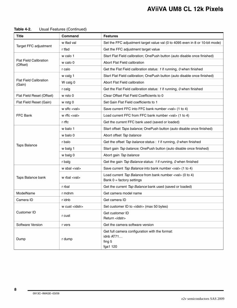
Table 4-2. Usual Features
Title Command Features
Output Mode
w mode 0 Set 4 output channels, 8-bit, medium configuration
w mode 1 Set 4 output channels, 10-bit, medium configuration
w mode 2 Set 4 output channels, 12-bit, medium configuration
w mode 3 Set 8 output channels, 8-bit, full configuration
r mode Get current output mode
Exposure Timew tint <val>
Set exposure time to <val>, from 1 to 65535
0.1 µs to 6553 µs by 0.1 µs step
r tint Get current exposure time
Line Periodw tper <val>
Set line period to <val> from 1 to 655350.1 µs to 6553 µs by 0.1 µs step
r tper Get current line period
Pre-amp Gainw pamp <val> Set pre-amp gain to: 0 (-9 dB), 1 (-6 dB), 2 (-3 dB), 3 (0 dB)
r pamp Get current pre-amp gain
Gainw gain <val> Set gain from -237 (-8.32 dB) to + 416 (14.6 dB) by step of 0.0351 dB
r gain Get current gain
Digital Gainw.gdig<val> Set digital gain from 0 to 255
DG (dB) = 20 log(1+val/64)r gdig
Offsetw offs <val> Set global offset from -4096 to +4095 in 12 bits LSB
r offs Get global offset
Synchronisation Mode
w sync 0 Set “Free run” mode
w sync 1 Set “Triggered mode with exposure time setting”
w sync 2 Set “Triggered mode with maximum exposure time”
w sync 3 Set “Triggered mode with exposure time controlled by one signal”
w sync 4 Set “Triggered mode with exposure time controlled by two signals”
r sync Get current Synchronisation mode
Signal Source
w srce 0 Set signal source to CCD sensor
w srce 1 Set signal source to pattern (Note:)
r srce Get current signal source
Flat Field Correction
w ffcp 0 Disable Flat Field Correction
w ffcp 1 Enable Flat Field Correction
r ffcp Get current FFC status
Flat Field Correction (FFC) adjustment
w ffad 0 Disable FFC adjustment
w ffad 1 Enable FFC adjustment
r ffad Get FFC adjustment state
70913C–IMAGE–03/09
e2v semiconductors SAS 2009
AViiVA UM8 CL 12k Pixels
Target FFC adjustmentw tfad val Set the FFC adjustment target value val (0 to 4095 even in 8 or 10-bit mode)
r tfad Get the FFC adjustment target value
Flat Field Calibration (Offset)
w calo 1 Start Flat Field calibration; OnePush button (auto disable once finished)
w calo 0 Abort Flat Field calibration
r calo Get the Flat Field calibration status: 1 if running, 0 when finished
Flat Field Calibration (Gain)
w calg 1 Start Flat Field calibration; OnePush button (auto disable once finished)
W calg 0 Abort Flat Field calibration
r calg Get the Flat Field calibration status: 1 if running, 0 when finished
Flat Field Reset (Offset) w rsto 0 Clear Offset Flat Field Coefficients to 0
Flat Field Reset (Gain) w rstg 0 Set Gain Flat Field coefficients to 1
FFC Bank
w sffc <val> Save current FFC into FFC bank number <val> (1 to 4)
w rffc <val> Load current FFC from FFC bank number <val> (1 to 4)
r rffc Get the current FFC bank used (saved or loaded)
Taps Balance
w balo 1 Start offset Taps balance; OnePush button (auto disable once finished)
w balo 0 Abort offset Tap balance
r balo Get the offset Tap balance status : 1 if running, 0 when finished
w balg 1 Start gain Tap balance; OnePush button (auto disable once finished)
w balg 0 Abort gain Tap balance
r balg Get the gain Tap Balance status: 1 if running, 0 when finished
Taps Balance bank
w sbal <val> Save current Tap Balance into bank number <val> (1 to 4)
w rbal <val>Load current Tap Balance from bank number <val> (0 to 4)
Bank 0 = factory settings
r rbal Get the current Tap Balance bank used (saved or loaded)
ModelName r mdnm Get camera model name
Camera ID r idnb Get camera ID
Customer ID
w cust <idstr> Set customer ID to <idstr> (max 50 bytes)
r custGet customer ID
Return <idstr>
Software Version r vers Get the camera software version
Dump r dump
Get full camera configuration with the format: idnb AT71…
fing 5
fga1 120
Table 4-2. Usual Features (Continued)
Title Command Features
80913C–IMAGE–03/09
e2v semiconductors SAS 2009

AViiVA UM8 CL 12k Pixels
Note: The test pattern must look like the following image.
Configuration
w scfg <val> Save current configuration into bank number <val> (1 to 4)
w rcfg 0 Load current configuration from factory bank (0)
w rcfg <val> Load current configuration from bank number <val> (1 to 4)
w rcfg 5 Load current configuration from integrator bank (5).
r rcfg Get the current configuration bank used (saved or loaded)
Table 4-2. Usual Features (Continued)
Title Command Features
Table 4-3. Advanced features
Title Command Features
Gain Adjustment w fga<i> <val>
Set gain adjustment for Tap#<i> (1 to 8),
from -128 (-0.26 dB) to 127 (0.26 dB), step 0.0021 dB
r fga<i> Get gain adjustment for Tap#<i> (1 to 8)
Clamp Adjustment w off<i> <val>
Set clamp adjustment for Tap#<i> (1 to 8), from -128 to 127 (12-bit LSB)
r off<i> Get clamp adjustment for Tap#<i> (1 to 8)
Flat Field Coefficients (Offset)
w ffco <addr> <nbrval> <val> …[crcval]
Write <nbrval> coefficients starting from the <addr> address.If [crcval] is added, the crc value is computed on the all the<val>.<addr> starts from 1. <val> is signed. <nbrval> is between 1 and 10
r ffco <addr> <nbrval> [crcreq]Read <nbrval> coefficients starting from <addr> address.If [crcreq] is equal to 1, the crc will be calculated on the <val>. <nbrval> is between 1 and 10. Output is : <val> …[crcval]
Flat Field coefficients (Gain)
w ffcg <addr> <nbrval> <val> … [crcval]
Write <nbrval> coefficients starting from the <addr> address. If [crcval] is added, the crc value is computed on the all the <val>.<addr> starts from 1
r ffcg <addr> <nbrval> [crcreq]Read <nbrval> coefficients starting from <addr> address. If [crcreq] is equal to 1, the crc will be calculate on the outputed value. Output is : <val> …[crcval]
VendorName r vdnm Get camera vendor name
Status r stat Get camera status
90913C–IMAGE–03/09
e2v semiconductors SAS 2009

AViiVA UM8 CL 12k Pixels
5. Camera Status The camera status can be read by r stat command (see Table 5-1).
The camera return is a 32-bit value.
Baudrate
w baud 1 Set CL RS232 baudrate to 9600 Bds (default value)
w baud 2 Set CL RS232 baudrate to 19200 Bds
w baud 6 Set CL RS232 baudrate to 57600 Bds
w baud 12 Set CL RS232 baudrate to 115200 Bds
w baud 24Set CL RS232 baudrate to 230400 Bds (for compatible frame grabber)
r baud Get current baudrate
Table 4-3. Advanced features
Title Command Features
Table 5-1. Camera Status
Bit Status Name Description
31 .. 22 not used Set to 0
21 .. 16 internal error
15 .. 12 not used Set to 0
11 FFC/Taps balance status1: in progress
0: disabled or finished
10FFC/Tap balance underflow
Updated after each calibration operation
1: output level is too high during calibration 0: calibration is well done
9 FFC/Tap balance overflowUpdated after each calibration operation1: output level is too low during calibration
0: calibration is well done
8 not used Set to 0
7 settings change1: states that at least one parameter has been modified and might be saved.
Set to 0 during save or restore operation
6 Tap Balance change
5 FFC change
4 .. 2 not used Set to 0
1 Trigger too fast set to 1 if trigger too fast, else 0
0 Waiting for trigger Set to 1 if no trigger in external trigger mode
100913C–IMAGE–03/09
e2v semiconductors SAS 2009
AViiVA UM8 CL 12k Pixels
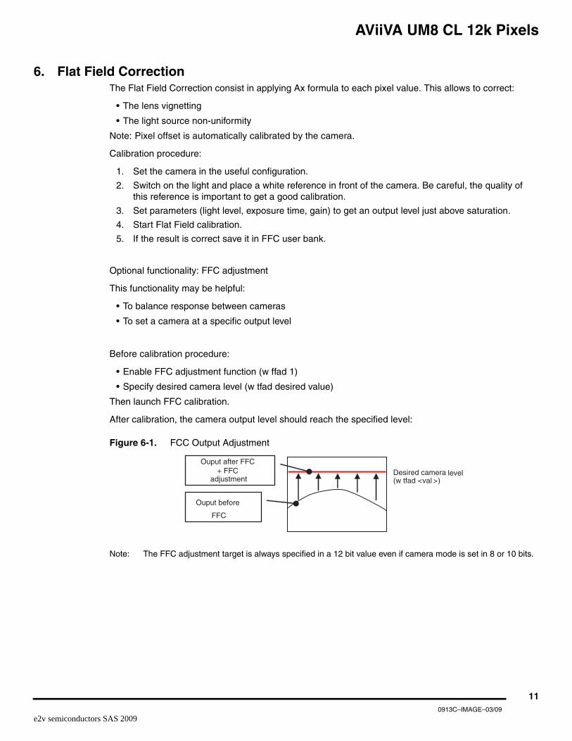
6. Flat Field CorrectionThe Flat Field Correction consist in applying Ax formula to each pixel value. This allows to correct:
• The lens vignetting
• The light source non-uniformity
Note: Pixel offset is automatically calibrated by the camera.
Calibration procedure:
1. Set the camera in the useful configuration.
2. Switch on the light and place a white reference in front of the camera. Be careful, the quality of this reference is important to get a good calibration.
3. Set parameters (light level, exposure time, gain) to get an output level just above saturation.
4. Start Flat Field calibration.
5. If the result is correct save it in FFC user bank.
Optional functionality: FFC adjustment
This functionality may be helpful:
• To balance response between cameras
• To set a camera at a specific output level
Before calibration procedure:
• Enable FFC adjustment function (w ffad 1)
• Specify desired camera level (w tfad desired value)
Then launch FFC calibration.
After calibration, the camera output level should reach the specified level:
Figure 6-1. FCC Output Adjustment
Note: The FFC adjustment target is always specified in a 12 bit value even if camera mode is set in 8 or 10 bits.
Desired camera level< >(w tfad val )
Ouput after FFC + FFC
adjustment
Ouput before
FFC
110913C–IMAGE–03/09
e2v semiconductors SAS 2009
AViiVA UM8 CL 12k Pixels
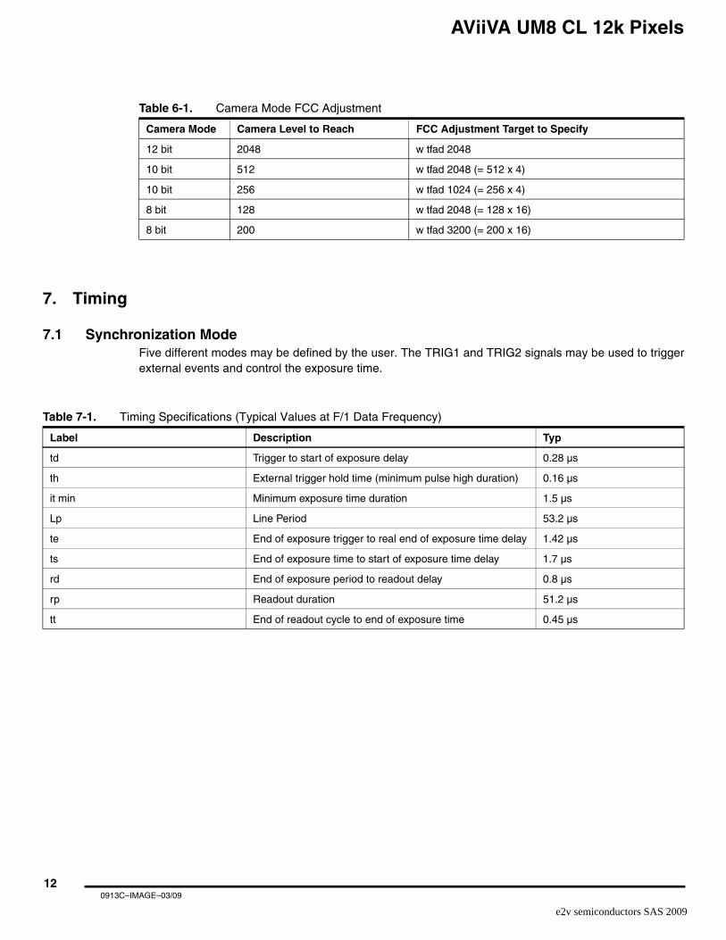
7. Timing
7.1 Synchronization ModeFive different modes may be defined by the user. The TRIG1 and TRIG2 signals may be used to triggerexternal events and control the exposure time.
Table 6-1. Camera Mode FCC Adjustment
Camera Mode Camera Level to Reach FCC Adjustment Target to Specify
12 bit 2048 w tfad 2048
10 bit 512 w tfad 2048 (= 512 x 4)
10 bit 256 w tfad 1024 (= 256 x 4)
8 bit 128 w tfad 2048 (= 128 x 16)
8 bit 200 w tfad 3200 (= 200 x 16)
Table 7-1. Timing Specifications (Typical Values at F/1 Data Frequency)
Label Description Typ
td Trigger to start of exposure delay 0.28 µs
th External trigger hold time (minimum pulse high duration) 0.16 µs
it min Minimum exposure time duration 1.5 µs
Lp Line Period 53.2 µs
te End of exposure trigger to real end of exposure time delay 1.42 µs
ts End of exposure time to start of exposure time delay 1.7 µs
rd End of exposure period to readout delay 0.8 µs
rp Readout duration 51.2 µs
tt End of readout cycle to end of exposure time 0.45 µs
120913C–IMAGE–03/09
e2v semiconductors SAS 2009
AViiVA UM8 CL 12k Pixels
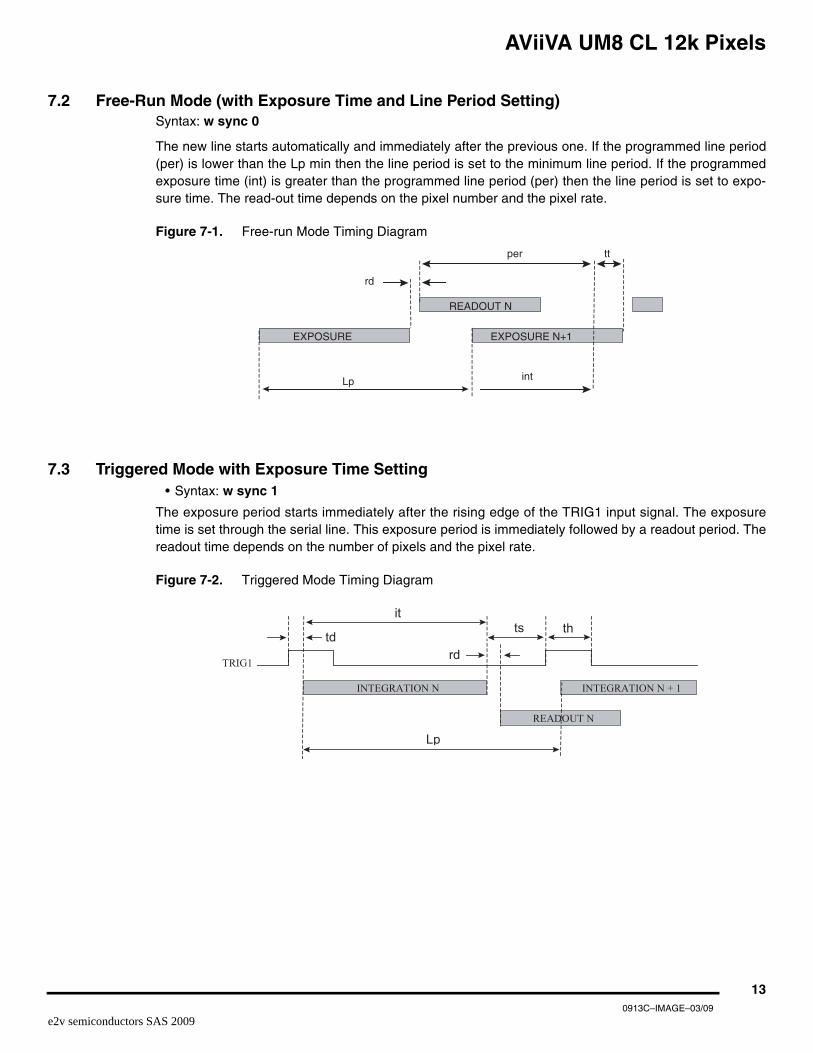
7.2 Free-Run Mode (with Exposure Time and Line Period Setting)Syntax: w sync 0
The new line starts automatically and immediately after the previous one. If the programmed line period(per) is lower than the Lp min then the line period is set to the minimum line period. If the programmedexposure time (int) is greater than the programmed line period (per) then the line period is set to expo-sure time. The read-out time depends on the pixel number and the pixel rate.
Figure 7-1. Free-run Mode Timing Diagram
7.3 Triggered Mode with Exposure Time Setting• Syntax: w sync 1
The exposure period starts immediately after the rising edge of the TRIG1 input signal. The exposuretime is set through the serial line. This exposure period is immediately followed by a readout period. Thereadout time depends on the number of pixels and the pixel rate.
Figure 7-2. Triggered Mode Timing Diagram
EXPOSURE
READOUT N
EXPOSURE N+1
rd
Lp
per tt
int
INTEGRATION N INTEGRATION N + 1
READOUT N
TRIG1
tdth ts
rd
it
Lp
130913C–IMAGE–03/09
e2v semiconductors SAS 2009

AViiVA UM8 CL 12k Pixels
7.4 Triggered Mode with Maximum Exposure TimeSyntax: w sync 2
The readout period and the next exposure period start immediately after the rising edge of the TRIG1input signal.
Figure 7-3. Triggered Readout Mode Timing Diagram
7.5 Triggered Mode with Exposure Time Controlled by One SignalSyntax: w sync 3
The exposure period starts immediately after the falling edge of TRIG1 and stops immediately after therising edge of TRIG1. This exposure period is immediately followed by a readout period. The readouttime depends on the number of pixels and the pixel rate. The pixels are reset while TRIG1 is high.
Figure 7-4. ITC Mode with One Signal Timing Diagram
INTEGRATION N INTEGRATION N+1
READOUT N-1
TRIG1
td
READOUT N
rd
it = Lp
th
Lp
INTEGRATION N INTEGRATION N+1
READOUT N-1
TRIG1
th
READOUT N
it
rd
td te
Lp
140913C–IMAGE–03/09
e2v semiconductors SAS 2009

AViiVA UM8 CL 12k Pixels
7.6 Triggered Mode with Exposure Time Controlled by Two SignalsSyntax: w sync 4
The rising edge of TRIG2 starts the exposure period. The rising edge of TRIG1 stops the exposureperiod and starts the readout period. The pixels are reset between the rising edge of TRIG1 and the ris-ing edge of TRIG2.
Figure 7-5. ITC Mode with Two Signals Timing Diagram
8. Output Data Timing
Figure 8-1. Timing Diagram
td
INTEGRATION N INTEGRATION N+1
READOUT N
TRIG2
TRIG1
it
te
rd
READOUT N-1
Lp
th
th
Table 8-1.
Label Description Min Typ Max
td STROBE to synchronized signals delay -3 ns +3 ns
LVAL
STROBE
DATA
Fist valid pixel Last valid pixel
td
td
td
150913C–IMAGE–03/09
e2v semiconductors SAS 2009

AViiVA UM8 CL 12k Pixels
9. Electrical Interface
9.1 Power SupplyIt is recommended to insert a two exposure A fuse between the power supply and the camera.
The power supply must provide 25W at power-on sequence.
Note: I = input, O = output, I/O = bi-directional signal, P = power/ground, NC = not connected
9.2 Camera ControlThe Camera Link interface provides four LVDS signals dedicated to camera control (CC1 to CC4). Onthe camera, two of them are used to synchronize the camera on external events.
Note: I = input, O = output, I/O = bi-directional signal, P = power/ground, NC = not connected
9.3 Video DataData and Enable signals are provided on the Camera Link interface
Note: I = input, O = output, I/O = bi-directional signal, P = power/ground, NC = not connected
Signal name I/O Type Description
PWR P DC power input : +12V to +24V (± 0.5V)
GND P Electrical and Mechanical ground
Table 9-1.
Signal name I/O Type Description
TRIG1 I RS664CC1 - Synchronization input (refer to “Output Data Timing” on page 15)
TRIG2 I RS664CC2 - Start exposure period in dual synchronization mode
Signal name I/O Type Description
OUT1-00 to OUT1-11 O RS644 Tap#1 Output pixel data (OUT1-00 = LSB, OUT1-11 = MSB)
OUT2-00 to OUT2-11 O RS644 Tap#2 Output pixel data (OUT2-00 = LSB, OUT2-11 = MSB)
OUT3-00 to OUT3-11 O RS644 Tap#3 Output pixel data (OUT3-00 = LSB, OUT3-11 = MSB)
OUT4-00 to OUT4-11 O RS644 Tap#4 Output pixel data (OUT4-00 = LSB, OUT4-11 = MSB)
OUT5-00 to OUT5-11 O RS644 Tap#5 Output pixel data (OUT5-00 = LSB, OUT5-11 = MSB)
OUT6-00 to OUT6-11 O RS644 Tap#6 Output pixel data (OUT6-00 = LSB, OUT6-11 = MSB)
OUT7-00 to OUT7-11 O RS644 Tap#7 Output pixel data (OUT7-00 = LSB, OUT7-11 = MSB)
OUT8-00 to OUT8-11 O RS644 Tap#8 Output pixel data (OUT8-00 = LSB, OUT8-11 = MSB)
STROBE O RS664Output data clock see “Output Data Timing” on page 15, data valid on the rising edge
LVAL O RS664 Line valid see “Output Data Timing” on page 15, active high signal
160913C–IMAGE–03/09
e2v semiconductors SAS 2009

AViiVA UM8 CL 12k Pixels
FVAL, as defined in the Camera Link standard, is not used. FVAL is permanently tied to 0 (low) level.
DVAL is not used. DVAL is permanently tied to one (high) level.
9.4 Serial CommunicationThe Camera Link interface provides two LVDS signal pairs for communication between the camera andthe frame grabber. This is an asynchronous serial communication based on RS-232 protocol.
The serial line configuration is:
• Full duplex/without handshaking
• 9600 bauds (default), 8-bit data, no parity bit, 1 stop bit. The baud rate can be set up to 230,400
10. Connector DescriptionAll connectors are on the rear panel.
Note: cables for digital signals must be shielded twisted pairs.
10.1 Power SupplyCamera connector type:Hirose HR10A-7R-6PB (male)
Cable connector type:Hirose HR10A-7P-6S (female)
Figure 10-1. Receptacle Viewed from the Rear Face of the Camera
Signal name I/O Type Description
SerTFG O RS644 Differential pair for serial communication to the frame grabber
SerTC I RS644 Differential pair for serial communication from the frame grabber
Table 10-1. Power Supply Connector Pinout
Signal Pin Signal Pin
PWR 1 GND 4
PWR 2 GND 5
PWR 3 GND 6
1
2
3
6
5
4
170913C–IMAGE–03/09
e2v semiconductors SAS 2009

AViiVA UM8 CL 12k Pixels
10.2 Camera Link ConnectorA standard Camera Link cable must be used to ensure full electrical compatibility.
The camera connector type is MDR-26 (female) ref. 10226-2210VE from 3M.
The cable connector type is a standard Camera Link cable.
Table 10-2. Camera Link Connector Pinout
Signal Pin Signal Pin
GND 1 GND 14
X0- 2 X0+ 15
X1- 3 X1+ 16
X2- 4 X2+ 17
Xclk- 5 Xclk+ 18
X3- 6 X3+ 19
SerTC+ 7 SerTC- 20
SerTFG- 8 SerTFG+ 21
CC1- 9 CC1+ 22
CC2+ 10 CC2- 23
CC3- 11 CC3+ 24
CC4+ 12 CC4- 25
GND 13 GND 26
180913C–IMAGE–03/09
e2v semiconductors SAS 2009
AViiVA UM8 CL 12k Pixels
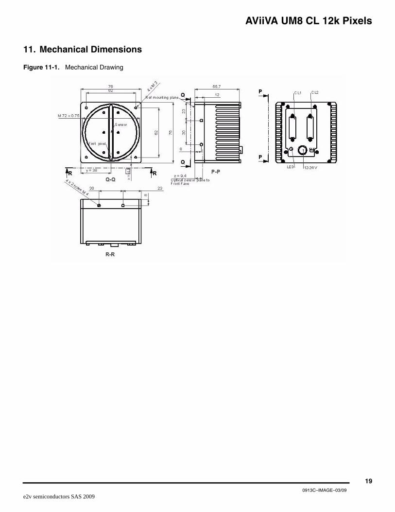
11. Mechanical Dimensions
Figure 11-1. Mechanical Drawing
190913C–IMAGE–03/09
e2v semiconductors SAS 2009
AViiVA UM8 CL 12k Pixels
12. Ordering Code
Note: Lens is not provided
Table 12-1. Ordering Code
Part Number Description
EV71YUM8CL1205-BA0Camera, power supply connector and CD-ROM including configuration software and documentation
200913C–IMAGE–03/09
e2v semiconductors SAS 2009
Whilst e2v has taken care to ensure the accuracy of the information contained herein it accepts no responsibility for the consequences of anyuse thereof and also reserves the right to change the specification of goods without notice. e2v accepts no liability beyond that set out in its stan-dard conditions of sale in respect of infringement of third party patents arising from the use of tubes or other devices in accordance with informa-tion contained herein.
How to reach usHome page: www.e2v.com
Sales offices:
Europe Regional sales office
e2v ltd
106 Waterhouse Lane
Chelmsford Essex CM1 2QU
England
Tel: +44 (0)1245 493493
Fax: +44 (0)1245 492492
mailto: [email protected]
e2v sas
16 Burospace
F-91572 Bièvres Cedex
France
Tel: +33 (0) 16019 5500
Fax: +33 (0) 16019 5529
mailto: [email protected]
e2v gmbh
Industriestraße 29
82194 Gröbenzell
Germany
Tel: +49 (0) 8142 41057-0
Fax: +49 (0) 8142 284547
mailto: [email protected]
Americas
e2v inc
520 White Plains Road
Suite 450 Tarrytown, NY 10591
USA
Tel: +1 (914) 592 6050 or 1-800-342-5338,
Fax: +1 (914) 592-5148
mailto: [email protected]
Asia Pacific
e2v ltd
11/F.,
Onfem Tower,
29 Wyndham Street,
Central, Hong Kong
Tel: +852 3679 364 8/9
Fax: +852 3583 1084
mailto: [email protected]
Product Contact:
e2v
Avenue de Rochepleine
BP 123 - 38521 Saint-Egrève Cedex
France
Tel: +33 (0)4 76 58 30 00
Hotline:
mailto: [email protected]
0913C–IMAGE–03/09e2v semiconductors SAS 2009
Top Related