


Languages
Pages
Legal


Crystallographic Characterization of Poly-Si Thin Films
Junichi NISHINO, Materials and Devices Development Center, SANYO Electric Co., Ltd.
Poly-Si has been used as a gate electrode material for many years on CMOS LSIs. As smaller and smaller LSIs continue to be
designed, even a minor difference in the crystal structure affects the electric property of MOS transistor. The typical thickness of
gate poly-Si films is about 200nm in 0.18µm rule LSIs. Normally, the poly-Si grains are around the same order of thickness, and
there are cases where a grain becomes a single crystal from the bottom to the top of film. In this case, the Boron penetration effect,
which is a serious problem in making LSIs, can easily occur due to ion channeling during ion implantation. To avoid this effect,
gate poly-Si films are made of double poly-Si layers. It is necessary to analyze the crystal structure of each layer of the double
poly-Si layer. In this experiment, to evaluate the characteristics of the crystal structure near the surface, we examined a test sample
of an amorphous-Si/poly-Si double layer film on Si wafer. The
in-plane X-ray diffraction was applied. The incident X-ray energy
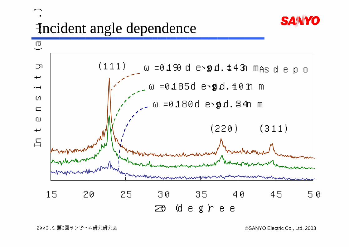
was 10.0keV. Figure 1 shows the in-plane diffraction patterns of the
amorphous-Si/poly-Si double layer film. The thickness of each layer
was the same as 100nm of amorphous-Si and poly-Si. In theω
=0.180 degree case, the diffraction pattern has only an
amorphous-Si structure. In the ω=0.190degree case, the diffraction
pattern has mainly a poly-Si structure. From these results, it has been
shown that it is possible to evaluate crystal structures of poly-Si thin
films in the depth direction by precise control in incident angle.
15 20 25 30 35 40 45 50
2θ (degree)
Inte
nsi
ty (
a.u.)
ω=0.180 deg、p.d.=34nm
ω=0.185 deg、p.d.=101nm
(111)
(311)(220)
ω=0.190 deg、p.d.=143nm
Fig. 1 In-plane XD spectra for amorphous-Si/ Poly-Si
double layer film with various incident angles.

2003.9.5 第3回サンビーム研究研究会 ©SANYO Electric Co., Ltd. 2003
Crystallographic characterization of poly-Si thin films
Materials and Devices Development Center BU,SANYO Electric Co., Ltd.
Junichi NISHINO
2003.9.5 第3回サンビーム研究研究会 ©SANYO Electric Co., Ltd. 2003
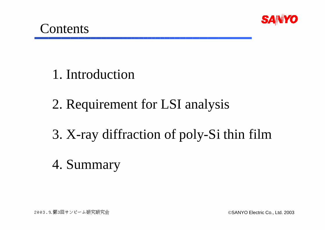
1. Introduction
2. Requirement for LSI analysis
3. X-ray diffraction of poly-Si thin film
4. Summary
Contents
2003.9.5 第3回サンビーム研究研究会 ©SANYO Electric Co., Ltd. 2003
Radio network
Cable network
OfficeOffice
HomeHomeCarCar
Handy phoneHandy phone
Terrestrial broadcasting
Satellite broadcasting
CATV
Telephone(ISDN,ADSL)
Homeserver
Digital stillcamera
PC
PhoneTV monitor
DVD
Video gameVideocamera
PC
Video printer
Home LAN
Living roomLiving roomBed roomBed room
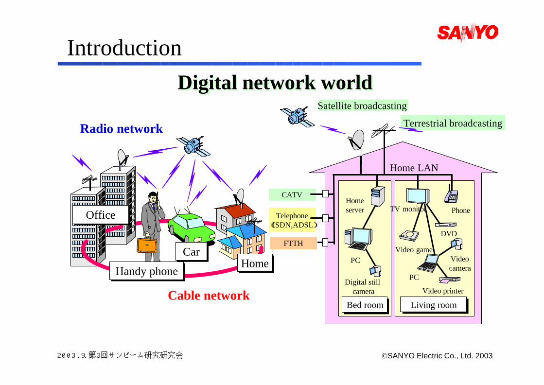
Digital network worldDigital network world
Introduction
FTTH

2003.9.5 第3回サンビーム研究研究会 ©SANYO Electric Co., Ltd. 2003
Key technology for system LSI
packagepackage devicedevice
designdesign processprocess
SoC(System on Chip)SoC(System on Chip)
calculationcalculation
PC
imageprocessing
imageprocessing
MPEG
input/outputinput/output
CCD/LCD
Storage media
W-CDMA
tele-communication
tele-communication
memorymemory
2003.9.5 第3回サンビーム研究研究会 ©SANYO Electric Co., Ltd. 2003
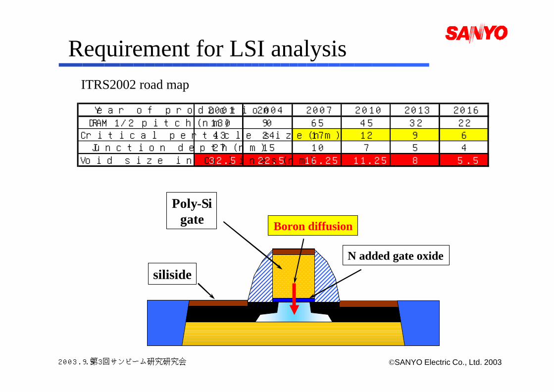
Requirement for LSI analysisITRS2002 road map
N added gate oxide
Poly-Sigate Boron diffusion
siliside
Year of production 2001 2004 2007 2010 2013 2016DRAM 1/2 pitch(nm) 130 90 65 45 32 22
Critical perticle size(nm) 43 24 17 12 9 6Junction depth(nm) 27 15 10 7 5 4
Void size in Cu lines(nm) 32.5 22.5 16.25 11.25 8 5.5

2003.9.5 第3回サンビーム研究研究会 ©SANYO Electric Co., Ltd. 2003
View
Element
Structure
Thickness
Analytical technique for LSI development
SEM, TEM, AFM
XRF, SIMS,EPMA, AES
XRD, XAFS
XRR , Ellipsometory
Make precise analytical technique using SR

2003.9.5 第3回サンビーム研究研究会 ©SANYO Electric Co., Ltd. 2003
Shrinkage of MOS-Tr ⇒ Boron diffusion problem
Prevent Boron diffusion ⇒ Double Poly-Si layer
Analyze crystallographic structure of thin Poly-Si films along depth direction
⇒ use X-ray diffractmetor
of BL16XU
Crystallographic characterization of thin films
Boron diffusion

2003.9.5 第3回サンビーム研究研究会 ©SANYO Electric Co., Ltd. 2003
BL16XU XRD・Parallel beam・Small size in incident beam:<0.2mm□・Energy of incident X-ray:tunable・Intensity:strong 3 order than rotation source・θ-2θ, thin film, in-plane
2θarm ditector
double slitsample

2003.9.5 第3回サンビーム研究研究会 ©SANYO Electric Co., Ltd. 2003
Poly-Si(50nm)diffraction
0
5
1 0
1 5
2 0
2 5
3 0
2 5 3 0 3 5 4 0 4 5 5 0 5 5 6 0 6 52 θ (d e g r e e )
coun
t (c
ps)
粉 末 回 折 装 置 C u K α 1 :4 0 k V ,3 0 m A
s t e p s c a n : 2 s e c / p o i n t 0 . 1 d e g / s t e pθ - 2θ
Lab.
BL16XU
0
5 0
1 0 0
1 5 0
2 0 0
2 5 0
3 0 0
2 0 2 5 3 0 3 5 4 0 4 5 5 02 θ ( d e g r e e )
coun
t (c
ps)
S P r i n g - 8 B L 1 6 X UE = 1 0 . 0 k e V
d o u b u l e s l i t : 0 . 0 9 d e gs t e p s c a n : 2 s e c / p o i n t 0 . 1 d e g / s t e p
i n c i d e n t a n g l e : 0 . 1 8 d e g

2003.9.5 第3回サンビーム研究研究会 ©SANYO Electric Co., Ltd. 2003
Layout of in-plane diffraction
Incident angle : about 0.18°
sample
diffraction
2θditector
Side view
Top view
Incident slit
double slit
Incident X-ray

2003.9.5 第3回サンビーム研究研究会 ©SANYO Electric Co., Ltd. 2003
Measurement condition
Incident X-ray・Energy 10.0KeV ・Beam size 0.1mmW×0.2mmH
Sample setting・Incident angle 0.170~0.200 degree
(precise angle control by tangent goniometor)・sample sticking to stage by oil
Detection・Detector: Scintillation counter・double slit 1.0mm + 1.0mm 0.29°
Measurement mode・2θ scan (θ fixed)

2003.9.5 第3回サンビーム研究研究会 ©SANYO Electric Co., Ltd. 2003
Total reflection on Si surfaceunder critical angle
over critical angle
almost reflected by sample surface
Penetrate into sample
Need precise incident angle control⇒ under 0.001°
penetration depth

2003.9.5 第3回サンビーム研究研究会 ©SANYO Electric Co., Ltd. 2003
X-ray reflectivity of Si surface
0.0
0.2
0.4
0.6
0.8
1.0
0.00 0.10 0.20 0.30 0.40incident angle (degree)
refle
ctiv
ity
E=10.0keV
θc = 0.180 deg

2003.9.5 第3回サンビーム研究研究会 ©SANYO Electric Co., Ltd. 2003
X-ray penetration depth into Si
1
10
100
1000
0.10 0.14 0.18 0.22 0.26incident angle (degree)
pene
trat
ion
dept
h (n
m)
E=10.0keV
θc = 0.180 degpenetration depth = 34nm

2003.9.5 第3回サンビーム研究研究会 ©SANYO Electric Co., Ltd. 2003
Sample setting accuracy (sample height)
Effective vertical beam width90μm
height accuracy : 1μm
X-ray monitor
sample
Incident X-ray
1.25 1.30 1.35 1.40 1.45sample height (mm)
inte
nsity
(a.
u.)
half position : 1.358mm
2003.9.5 第3回サンビーム研究研究会 ©SANYO Electric Co., Ltd. 2003
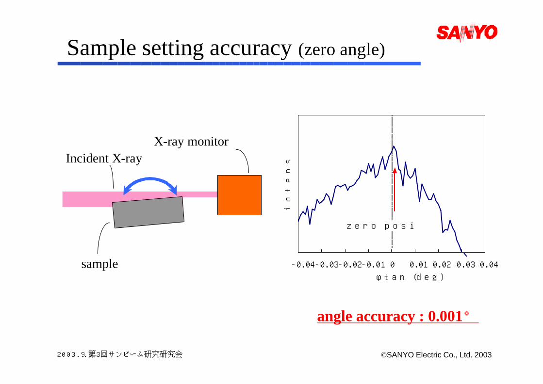
Sample setting accuracy (zero angle)
-0.04 -0.03 -0.02 -0.01 0 0.01 0.02 0.03 0.04φtan (deg)
inte
nsity
(a.
u.)
zero position : +0.001deg
angle accuracy : 0.001°
X-ray monitor
sample
Incident X-ray

2003.9.5 第3回サンビーム研究研究会 ©SANYO Electric Co., Ltd. 2003
Test piece 1(Amo/Poly double layer)
a-Si 100nm
SiO2 25nm
Si wafer
Poly-Si 100nm
2003.9.5 第3回サンビーム研究研究会 ©SANYO Electric Co., Ltd. 2003
Incident angle dependence
As depo
15 20 25 30 35 40 45 502θ (degree)
Inte
nsity
(a.
u.)
ω=0.180 deg、p.d.=34nm
ω=0.185 deg、p.d.=101nm
(111)
(311)(220)
ω=0.190 deg、p.d.=143nm

2003.9.5 第3回サンビーム研究研究会 ©SANYO Electric Co., Ltd. 2003
Test piece 2(Amo/Poly double layer)
a-Si 150nm
SiO2 25nm
Si wafer
Poly-Si 50nm
Thick amorphous Si layer to measure annealing effect

2003.9.5 第3回サンビーム研究研究会 ©SANYO Electric Co., Ltd. 2003
Crystallographic change by annealing
15 20 25 30 35 40 45 502θ (degree)
Inte
nsity
(a.
u.)
ω=0.170 deg
ω=0.200 deg
(111)
(220) (311)
As depo

2003.9.5 第3回サンビーム研究研究会 ©SANYO Electric Co., Ltd. 2003
15 20 25 30 35 40 45 502θ (degree)
Nor
mal
ized
Inte
nsity
(a.
u.)
ω=0.170 deg
ω=0.200 deg
(111)
(220) (311)
Crystallographic change by annealing
After 1000℃ 5sec N2

2003.9.5 第3回サンビーム研究研究会 ©SANYO Electric Co., Ltd. 2003
Crystallographic change by annealing
49nm
53nm
12nm
---
grain size
82nm
82nm
13nm
---
grain size
FWHMgrain size
FWHMFWHM
52nm
52nm
14nm
---
0.200°
0.170°
0.200°
0.170°
Incident angle
index
0.13°0.13°0.08°9.5nm
after anneal
---------9.5nmas
depo
0.14°0.13°0.08°204nm
0.6°0.5°0.5°204nm
311220111Penetra
tion depth
FWHMs of each index are almost same value after anneal treatment
⇒ change uniform crystallographic structure in depth direction

2003.9.5 第3回サンビーム研究研究会 ©SANYO Electric Co., Ltd. 2003
・High S/N in-plane XRD measurement forthin film is available using BL16XU XRDsystem.
・It is possible to evaluate crystal structures of poly-Si thin films in the depth direction byprecise control in incident angle of 0.001°.
・Crystallographic characterization of SOI and epitaxial layer is next step.
Summary
Top Related