


Languages
Pages
Legal


BearWorks BearWorks
MSU Graduate Theses
Fall 2016
Comparative Characterization Of Molybdenum Oxide Thin Films Comparative Characterization Of Molybdenum Oxide Thin Films
Grown On Various Substrates Using Temporally Different Pulsed Grown On Various Substrates Using Temporally Different Pulsed
Laser Deposition Techniques Laser Deposition Techniques
Krishna Harsha Puppala
As with any intellectual project, the content and views expressed in this thesis may be
considered objectionable by some readers. However, this student-scholar’s work has been
judged to have academic value by the student’s thesis committee members trained in the
discipline. The content and views expressed in this thesis are those of the student-scholar and
are not endorsed by Missouri State University, its Graduate College, or its employees.
Follow this and additional works at: https://bearworks.missouristate.edu/theses
Part of the Materials Science and Engineering Commons
Recommended Citation Recommended Citation Puppala, Krishna Harsha, "Comparative Characterization Of Molybdenum Oxide Thin Films Grown On Various Substrates Using Temporally Different Pulsed Laser Deposition Techniques" (2016). MSU Graduate Theses. 3040. https://bearworks.missouristate.edu/theses/3040
This article or document was made available through BearWorks, the institutional repository of Missouri State University. The work contained in it may be protected by copyright and require permission of the copyright holder for reuse or redistribution. For more information, please contact [email protected].
COMPARATIVE CHARACTERIZATION OF MOLYBDENUM OXIDE THIN
FILMS GROWN ON VARIOUS SUBSTRATES USING TEMPORALLY
DIFFERENT PULSED LASER DEPOSITION TECHNIQUES
A Masters Thesis
Presented to
The Graduate College of
Missouri State University
TEMPLATE
In Partial Fulfillment
Of the Requirements for the Degree
Master of Science, Materials Science
By
Krishna Harsha Puppala
December 2016

ii
Copyright 2016 by Krishna Harsha Puppala

iii
COMPARATIVE CHARACTERIZATION OF MOLYBDENUM OXIDE THIN
FILMS GROWN ON VARIOUS SUBSTRATES USING TEMPORALLY
DIFFERENT PULSED LASER DEPOSITION TECHNIQUES
Physics, Astronomy and Materials Science
Missouri State University, December 2016
Master of Science
Krishna Harsha Puppala
ABSTRACT
Pulsed Laser Deposition (PLD) technique, with its vast tunability in terms of thin film
fabrication has been the center of this study. By changing the temporal component of the
laser source used for deposition into the femtosecond (fs) regime, interesting structural,
morphological changes can be achieved which may prove to be beneficial for
photocatalytic applications. In particular, molybdenum oxide thin films, which are the
less well-studied and potentially newer candidates for photocatalysis applications have
been chosen for investigation. Hence, a detailed characterization study of molybdenum
oxide thin films synthesized using femtosecond-based (f-PLD) and nanosecond-based (n-
PLD) techniques, was carried out in terms of their structural, morphological, surface
chemical/ electronic states and vibrational properties using X-ray diffraction, scanning
electron microscopy, X-ray photoelectron spectroscopy and Raman spectroscopy. The f-
PLD technique was found to produce more favorable molybdenum oxide thin films
deposited on glass for surface-related applications, in terms of having a higher surface to
volume ratio, than the n-PLD technique. A related simultaneous study of substrate-based
effect on the thin films produced using n-PLD system, also revealed both variation
among the morphological, structural, and electronic (in terms of Mo oxidation state)
properties depending upon the nature of the substrate used to synthesize the molybdenum
oxide thin films. Special cases of thin films on epitaxial substrates (Si, sapphire) have
been characterized to determine the parameters necessary for fabricating highly-textured
thin films with large surface-area to volume ratio, which is key to efficient photo-
catalysts.
KEYWORDS: Thin films, Raman, SEM, XPS, Pulsed Laser Deposition
This abstract is approved as to form and content
_______________________________
Robert A Mayanovic, PhD
Chairperson, Advisory Committee
Missouri State University

iv
COMPARATIVE CHARACTERIZATION OF MOLYBDENUM OXIDE THIN
FILMS GROWN ON VARIOUS SUBSTRATES USING TEMPORALLY
DIFFERENT PULSED LASER DEPOSITION TECHNIQUES
By
Krishna Harsha Puppala
A Masters Thesis
Submitted to the Graduate College
Of Missouri State University
In Partial Fulfillment of the Requirements
For the Degree of Master of Science, Materials Science
December 2016
Approved:
_______________________________________
Robert A Mayanovic, PhD
_______________________________________
Mahua Biswas, PhD
_______________________________________
Fei Wang, PhD
_______________________________________
Julie Masterson, PhD: Dean, Graduate College

v
ACKNOWLEDGEMENTS
I will always be thankful and indebted to my advisor, Dr. Robert Mayanovic for
his unending support and patience towards my thesis completion. His enthusiasm to
mentoring and teaching others has inspired me all along the way. It has been his
continuous belief in my success that had led to my successful completion of this thesis. I
shall always be indebted to Dr. Mahua Biswas and Dr. Fei Wang for serving on my thesis
committee and guiding me at all crucial stages of this work. I shall always be grateful to
Dr. Kartik Ghosh, Dr. David Cornelison and Dr. Ridwan Sakidja for helping me at
various stages of this thesis.
My special thanks to fellow colleagues, Mr. Delower Hossain, Mr. Tamzid Ibn
Minhaj, Mr. Anthony Pelton and Mr. Abdullah Mamun for helping me professionally
with this research work. I must specially thank Jake Connor, of US Photonics for
collaborating with our research group under Dr. Robert Mayanovic and showing
immense interest in this work. I would like to thank Laura Rios, the department’s
administrative assistant, whose constant help throughout my graduate study is worth
mentioning. Also, I would like to acknowledge Rishi Patel, for providing help with the
XPS data collection.
It was the never ending faith in my success among my parents, friends and family
that made this work possible. Finally, I would like to thank the Graduate College for
providing partial support towards this research work.
I dedicate this thesis to Madhavi (Mother) and Mohan Rao (Father).

vi
TABLE OF CONTENTS
Chapter 1: Introduction ........................................................................................................1
Femtosecond Pulsed Laser Deposition ....................................................................3
Molybdenum Oxide Thin Films as Candidate Materials .........................................4
Annealing Effects and Substrate Based Studies ......................................................6
Chapter 2: A Comparative Characterization Study of Molybdenum Oxide Thin Films
Grown Using Femtosecond and Nanosecond Pulsed Laser Deposition ..............................8
Abstract ....................................................................................................................8
Introduction ..............................................................................................................9
Experimental ..........................................................................................................10
Results and Discussion ..........................................................................................11
Conclusion .............................................................................................................16
Acknowledgments..................................................................................................17
References ..............................................................................................................17
Chapter 3: Substrate Effects on the Structural and Morphological Aspects of Molybdenum
Oxide Thin Films Synthesized by Nanosecond Pulsed Laser Deposition .........................19
Abstract ..................................................................................................................19
Introduction ............................................................................................................19
Experimental Details ..............................................................................................22
Results and Discussion ..........................................................................................25
Conclusions ............................................................................................................46
Acknowledgments..................................................................................................47
References ..............................................................................................................47
Supplementary Information (SI) ............................................................................50
Chapter 4: Summary ..........................................................................................................57
References for Introduction ...............................................................................................59

vii
LIST OF TABLES
Table 2.1. Summary of fitting results of the high-resolution XPS data representing the
Mo 3d spin orbital component peak parameters for the post-annealed f-PLD and n-PLD
thin films. ...........................................................................................................................15
Table 3.1. Summary of the XPS survey scan elemental quantification measured from
molybdenum oxide thin film on sapphire substrate ...........................................................37
Table 3.2. Summary of fitting results of the high-resolution XPS spectra measured from
the MoOx/sapphire thin film ..............................................................................................40
Table 3.3. The Raman spectral deconvolution and analysis as compared to Literature
values of various oxides of molybdenum in the bulk form ...............................................43
Table S3.1. Summary of fitting results of the high-resolution XPS spectra measured from
MoOx/SiO2/Si thin film. .....................................................................................................53
Table S3.2. Summary of the XPS survey scan elemental quantification measured from
molybdenum oxide thin film on silicon substrate ..............................................................54

viii
LIST OF FIGURES
Figure 1.1. A schematic of the excimer laser-based PLD chamber setup used for the n-
PLD based thin films ...........................................................................................................3
Figure 1.2. The crystal structures of (a) orthorhombic α- MoO3 (b) ReO3 –type
monoclinic β- MoO3 ............................................................................................................6
Figure 2.1. SEM micrographs (clockwise) showing the differences in the morphology of
thin films prepared using f-PLD (a & b) and n-PLD (c & d). ...........................................12
Figure 2.2. (a) Left panel- XRD patterns showing of pre-annealed n-PLD (dotted line)
and f-PLD (solid line) thin films. (b) Right panel- Post-annealed XRD patterns showing
n-PLD (dash-dotted line) and f-PLD (solid line) thin films and peak locations of the
orthorhombic α-MoO3 phase; the majority of the remaining peaks are attributed to the
MoO2 phase ........................................................................................................................13
Figure 2.3. XPS high-resolution spectrum showing the fitted Mo 3d doublet peak for (a)
f-PLD thin film and (b) n-PLD thin film annealed at 450 °C ............................................14
Figure 2.4. Raman spectra of f-PLD (solid line) and n-PLD thin films (dash-dotted line)
(a) prior- annealing & (b) post-annealing at 450 °C for up to 20 hours ............................16
Figure 3.1. SEM micrograph of MoOx thin films on Si substrate (a & b), sapphire
substrate (c & d), both annealed at 450 °C for 6 hours (at various magnifications) ..........28
Figure 3.2. (a) SEM image of MoOx/Si thin films after annealing for total of 12 hours,
shows development of terrace-like features on a large scale (the inset is of a tilted scan
close-up image (tilt angle-30°) justifying the clear faceting aspect in a step-like nature, 2
μm scale). (b) some regions also possessed highly strained, rod-like feature in
combination with the faceted planes .................................................................................29
Figure 3.3. SEM micrograph of post-annealed thin film (for 20 hours) on glass substrate
(n-PLD, Ts=RT) .................................................................................................................30

ix
Figure 3.4. AFM 3D images of post-annealed samples of MoOx thin films on: sapphire
substrate (left) with the depth (z-axis) of 41.1 nm and Si substrate (right) with the depth
(z-axis) of 81.4 nm. The scale bar in the xy-plane is 2 μm x 2 μm ...................................31
Figure 3.5. AFM 2D images (2 μm x 2 μm) of post- annealed thin samples of MoOx thin
films on (a) sapphire substrate (b) Si substrate ..................................................................32
Figure 3.6. Typical XRD pattern of the MoOx/Si thin film after thermal treatment (450
°C-12 hours). The inset shows the pseudo-amorphism from the shorter atomic planes....35
Figure 3.7. XRD pattern of the MoOx/sapphire thin film after thermal treatment (450 °C-
6 hours) ..............................................................................................................................36
Figure 3.8. The survey scans of thin films on both the substrates: sapphire (Black-Top)
and Si (Red-Bottom) showing the presence of only the constituent elements present in the
thin films (Mo, O) and substrates (Al from sapphire; Si from silicon substrate) ..............38
Figure 3.9. The high-resolution (HR) spectra fitting of MoOx/sapphire thin film showing
O1s (left) and Mo3d (right) components. The fitting parameters and constraints are partly
based on the output from the survey scan regarding the possible components and their
corresponding peak positions .............................................................................................39
Figure 3.10. XPS high-resolution (HR) spectra fitting of MoOx/Si thin film with
corresponding O1s (left) and Mo3d (right) component. The fitting parameters and
constraints are based partly based on the output from survey scan regarding the possible
components and their peak positions .................................................................................41
Figure 3.11. Raman analysis (50-1050 cm-1) of MoOx thin film on SiO2/Si (Top-Red) and
on the sapphire substrate (Bottom-Black), both at Ts = 300 °C, after post-annealing at 450
°C for 12 hours and 6 hours respectively. The high intensity Si single crystal Raman band
(~520.7 cm-1) is chopped off for consistency. The band positions of various vibrational
modes in the MoOx have been noted (Blue) ......................................................................42
Figure S3.1. The morphology of the MoOx/sapphire thin films in the as-deposited
condition (a), which shows only smooth surface and the elemental quantification using
SEM-EDX (b) at higher working distance (W. D=13.6 mm) and 5 keV ..........................51

x
Figure S3. 2. (a) A typical XRD pattern of MoOx/SiO2/Si film in the as-deposited
condition shows only the peak of Si substrate other than the majorly amorphous
background. (b) The XRD pattern with unique features of mixed-amorphous/crystalline
features in the thin film on sapphire substrate ...................................................................52
Figure S3.3. Photographs of the MoOx thin film on Si (100) substrate in the, (a) as-
deposited condition (fresh from the PLD chamber, which was used for annealing after
cutting on one edge (as shown), in (b) just before annealing on the Linkam Stage, and
finally upon annealing at 450 °C, for 12 hours ..................................................................55
Figure S3.4. The MoOx/sapphire thin film in the (a) as–deposited condition just before
annealing, and (b) just after annealing at 450 °C for 6 hours ............................................55

1
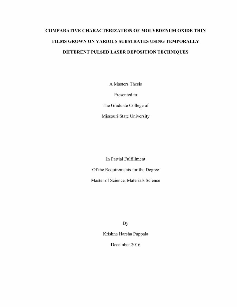
CHAPTER 1: INTRODUCTION
The pulsed laser deposition (PLD) technique is a highly versatile method for thin
film deposition performed by ablating a target with a high energy pulsed laser in a
controlled vacuum chamber. In particular, it is unique in that the technique allows for the
deposition of a wide range of thin films (e.g., metal oxides, nitrides, germinates,
arsenides, etc.) not accessible to other deposition techniques. While the target material of
interest is being ablated by the pulsed UV-laser, a plasma plume is created consisting of
high velocity energetic species. These in turn travel towards a nearby substrate, which
may or may not be heated, to subsequently condense on its surface forming a
stoichiometric thin film [1]. The main advantage of the PLD technique is that it can
create materials with complex stoichiometry while keeping the particle size distribution
to a small range, while keeping the impurities to relatively low level [2]. The high-power
pulsed UV-lasers in a vacuum chamber environment enable the creation of a variety of
stoichiometric oxide films, especially when used in combination with a reactive
background gas atmosphere. Although the reactive atmosphere does not affect the laser
beam path and its interaction with target materials, it does have a bearing on the plasma
plume creation and its kinetics [3]. Over the years, the PLD technique has been
developed into a reliable methodology for the fabrication of high purity, functional thin
films necessary for device manufacturing. The high purity of the thin films created in this
way is an outstanding feature of the PLD technique; nevertheless, it should be noted that
this is highly dependent upon the level of vacuum in the chamber and care taken to
ensure high purity of substrate, ambient gas and target used in PLD. The disadvantage of

2
this fabrication process while using the nanosecond –based laser is the formation of bulk
particulates which travel within the created plume toward the colder substrate surface
during deposition. These bulk-type deposits (often called “splashing”) are due to the
extreme thermal shock imposed upon the target surface by the impinging laser pulses.
More recently, some developments have been made to counter these relatively slow-
moving particulates from the plasma, such as, a velocity-based mechanical particle filter
[3]. However, the thrust of PLD technique development has concentrated on the removal
of these particulates during initial creation at the source, i.e., at the target. Irrespective of
the type of the deposition technique of the thin films, the adhesion of the thin films to the
substrate also plays a key role in its usefulness for practical applications. The main
reasons behind adhesion of thin films could be primarily due to atomic bonds created by
the interaction of the two surfaces, or mechanical locking and friction due to surface
texture and an inter-diffusion transition layer formed at the interface [4]. Hence, there is a
dual control nature embedded in the PLD synthesis of thin films: one being the ablation
mechanism during the deposition process, and the other being the interface control of the
substrate and thin film, during and after deposition process. These two primary control
variables should be well understood and monitored before the production of a thin film
applicable to any type of real-life purpose.
Whereas the majority of current research is focused on the synthesis of
nanostructured thin films by PLD using nanosecond (ns)-based lasers (pulse duration~10-
9 seconds), the use of femtosecond (fs) –based laser (pulse duration<10-15 seconds) has
been made sparingly. A typical nanosecond excimer laser-based PLD chamber is
represented in the schematic diagram provided in F 1.1 [5]. While many other studies
3
were made using variable stoichiometric targets to create complex multicomponent
oxides and compounds, considerably less is known on the usage of picosecond- &
femtosecond-based laser (pulse duration~10-12 - 10-15 seconds order magnitude). As such,
the use of femtosecond-based laser for PLD could be a potential game changer for
production of thin films for photocatalytic applications. This research in part attempts to
fill upon the gap produced in between the comprehension of both these techniques and
their applicability to create high surface-area to volume ratio structures.
Figure 1.1. A schematic of the excimer laser-based PLD chamber setup used for the n-
PLD based thin films [5].
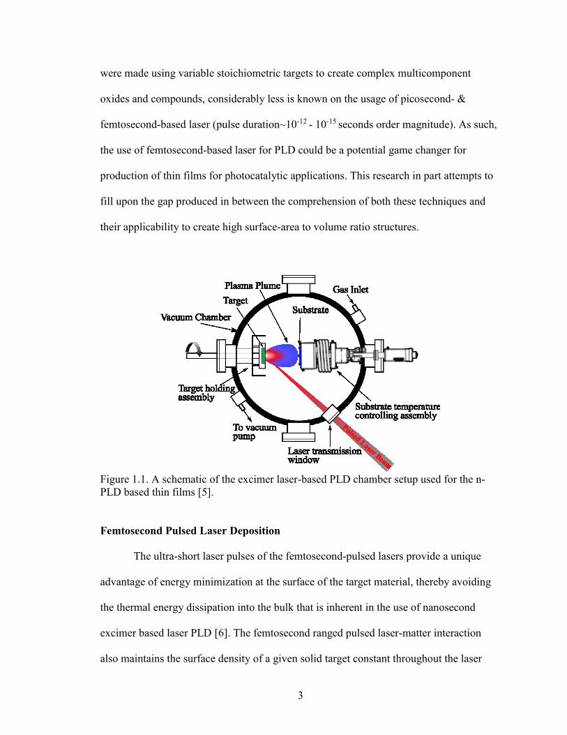
Femtosecond Pulsed Laser Deposition
The ultra-short laser pulses of the femtosecond-pulsed lasers provide a unique
advantage of energy minimization at the surface of the target material, thereby avoiding
the thermal energy dissipation into the bulk that is inherent in the use of nanosecond
excimer based laser PLD [6]. The femtosecond ranged pulsed laser-matter interaction
also maintains the surface density of a given solid target constant throughout the laser

4
ablation. This enables a cleaner ablation process that avoids creation of molten droplets
and enhances the synthesis of stoichiometrically pure thin films [1]. In addition, the
ultrashort pulsed ablation method inherent in the use of the femtosecond-pulsed laser
tends to reduce the formation of the splashes on the substrates, which is a major issue in
the conventional excimer laser processes, especially in the deposition of metal oxide
systems. This is because the short-pulse interactions limit the relaxation dynamics and the
seeking of thermal equilibrium by the target species (i.e. molecular, atomic, etc.), which
is in contrast to the interactions produced by the longer nanosecond pulses. Hence, the
result is an achievement of highest possible laser intensities (>1013 W/cm2), when
compared to any known laser ablation method used till date [6]. The femtosecond lasers
are relatively newer types of temporally adjusted photon sources which have been
predominantly used for industrial micro-machining applications demanding high
precision. Use of these femtosecond high-intensity lasers provides an ablation process
whereby the multiphoton ionization and avalanche ionization are the determining
absorption mechanisms within the surface of the target material. These mechanisms
provide a means by which the lasers’ energy is absorbed to a maximum extent at the
target, which would not be possible using a conventional low intensity nanosecond-based
laser.
Molybdenum Oxide Thin Films as Candidate Materials
The orthorhombic phase of molybdenum trioxide (α-MoO3), has the basis of
MoO6 octahedral unit repeated in an orthorhombic lattice. These octahedral building
blocks are corner-shared so as to form chains of edge-shared layers (F 1.2 (a)). These

5
layers are arranged on top of one another in a zig-zag manner where the layers are held
together by Van der Waals forces [7]. The crystal structure of α-MoO3 consists of a
layered structure of two octahedral MoO6 layers, joined by double covalent forces in the
a and c axes. The layers are attracted by Van der Waal’s forces along the b axes [8]. The
anisotropic growth of these crystallites is a consequence of distorted MoO6 octahedral
units (unequal Mo-O distances along the O-Mo-O bond direction) which form the lattice
of MoO3 [9]. It is the layering inherent in the alpha phase that makes it highly suitable for
many practical applications, especially in catalysis, battery storage technology, smart
windows, and other electrochromic-based technologies. The orthorhombic structure is
thermodynamically most stable polymorph of MoO3, even though it has numerous
oxidation states ranging from +2 to +6 with each having its own crystal system. Sub-
stoichiometric thin film oxides have been studied recently for specialized applications. In
its native form, MoO3 is a wide band gap n-type semiconductor transition metal oxide.
The semiconductor band gap is generally found to be approximately 2.6 eV, but also
varies from 2.8 – 3.2 eV. The oxide is also known to have the metastable-monoclinic (β-
MoO3) and hexagonal (h-MoO3) phases. While the monoclinic β-MoO3 has a
resemblance to the perovskite-like structure (ReO3-type) with a continuous network of
corner-shared MoO6 octahedral units (F 1.2 (b)), the hexagonal phase is also a metastable
polymorph with a zig-zag arrangement of distorted MoO6 octahedra in a cis-position
[10]. Molybdenum dioxide (MoO2) forms when the metal is in the Mo4+ oxidation state.
The MoO2 crystal structure consists of a distorted rutile-type tetragonal crystalline
arrangement [11]. It has been shown that the phase transition of β to α- MoO3 occurs at
above 350 °C.

6
The recent past has seen the growth of MoO3 films for gas sensors, lithium ion
batteries, electrochromic device applications and many more. The principal techniques
used for synthesis of metal oxide films have been (RF and DC) sputtering, chemical
vapor deposition (CVD), and PLD techniques. PLD has been used for growth of
molybdenum oxide thin films by Kuhaili et al [12] & Pardo et al [13] and others.
Figure 1.2. The crystal structures of (a) orthorhombic α- MoO3 (b) ReO3 –type
monoclinic β- MoO3 [7].
Annealing Effects and Substrate Based Studies
While it has been largely accepted that annealing at temperatures above 400 °C in
requisite oxygen-bearing atmospheres leads to ideal stoichiometry attainment of O: Mo =
3:1, there has been debate as to what effect the temperature choice has on the
crystallization of these thermodynamically stable hexavalent phases. Annealing in
oxidizing temperature above 400 °C has been shown to accommodate the improvement
of the atomic ordering within the films [14]. However, another important aspect in

7
temperature selection is whether the desired short and long range atomic ordering is
achieved at the chosen annealing temperature.
In Chapter 2 of this thesis, a comparative study of femtosecond- and nanosecond-
based PLD of molybdenum oxide thin film deposited on glass substrates is presented.
This work has been published in MRS Advances [15]. In Chapter 3 of this thesis, I
present a comparative study of molybdenum oxide thin films synthesized using
nanosecond-based PLD and deposited on glass, silicon and sapphire substrates. This
work is in preparation for submission to the journal Thin Solid Films.

8
CHAPTER 2: A COMPARATIVE CHARACTERIZATION STUDY OF
MOLYBDENUM OXIDE THIN FILMS GROWN USING FEMTOSECOND AND
NANOSECOND PULSED LASER DEPOSITION
Abstract
Group 6 transition metal oxide thin films are in large demand for photocatalysis,
heterogeneous catalysis, fuel cell, battery and electronic applications. Pulsed laser
deposition offers an inexpensive method for the preparation of nanostructured thin films
that may be suitable for heterogeneous catalysis. I have synthesized molybdenum oxide
thin films using two types of pulsed laser deposition (PLD). The first method utilizes
femtosecond laser-based PLD (f-PLD) while the second method uses an excimer
(nanosecond) laser-based PLD (n-PLD). The PLD films have been deposited using f-PLD
and, separately, n-PLD on glass and silicon substrates and subsequently annealed to 450
°C for up to 20 hours in air using a Linkam stage. SEM, XRD and Raman spectroscopic
characterization shows that the f-PLD films are substantially more textured and partially
crystalline prior to annealing whereas the n-PLD-grown thin films are much smoother
and predominantly amorphous. A 3-dimensional nano-crystalline structure is evident in
the post-annealed f-PLD synthesized thin films, which is desirable for catalytic
applications. XPS elemental analysis shows that the stoichiometry of the f-PLD and n-
PLD thin films is consistent with the presence of MoO2 and MoO3. My results are
discussed in terms of thin film growth models suitable for f-PLD vs n-PLD.

9
Introduction
The transition metal oxide thin films have a significant role to play in major
energy applications like photocatalysis, heterogeneous catalysis, electrochromic and
photochromic devices etc. [1]. Molybdenum trioxide (MoO3) is highly useful as a
selective catalyst for hydrocarbon oxidation [2, 3]. Crystalline molybdenum trioxide
occurs in two major crystal phases, namely orthorhombic α-MoO3 and monoclinic β-
MoO3. The α-MoO3 phase is thermodynamically stable and the β-MoO3 is metastable [4].
While the amorphous molybdenum oxide thin films have a perovskite-like structure
consisting of corner-shared MoO6 octahedra, they have been shown to exhibit more
photochromic response than their crystalline counterparts [1]. The band gap of
molybdenum trioxide can be modified by various means, including introduction of
dopants and by ionic (e.g., alkali ions) intercalation. The synthesis of these thin films falls
into three major categories: vapor, liquid and solid phase deposition techniques. The
common element of these techniques is the aim to increase the planar area of the
preferred growth of the layered material, have control over the film thickness, and to
produce films having good crystallinity [4]. There is currently considerable interest in the
relatively low-cost synthesis of thin films having novel nanostructured properties for
projected future applications in energy harvesting and industry. Femtosecond lasers may
find suitability for use in thin film deposition as these have higher intensities and shorter
pulse durations than nanosecond lasers currently used in pulsed laser deposition (PLD).
Femtosecond laser PLD (f-PLD) has been used in the past by a handful of workers for
deposition of thin films where it has shown promise for synthesis of materials having
novel properties [5-7]. Additionally, f-PLD films may eliminate the issue of macroscopic

10
droplet formation, which is considered to be the result of thermal effects during the laser-
matter interaction [8]. Herein, I discuss some of the results from the growth of
molybdenum oxide thin films using f-PLD and compare those to the characteristics of
molybdenum oxide thin films prepared using nanosecond laser PLD (n-PLD).
Experimental
The MoO3 targets used for pulsed laser deposition were prepared from pure
(>99%) MoO3 powder (Sigma-Aldrich). The powders were ground very finely using
mortar and pestle and compressed into pellets using a 10 Metric-ton hydraulic press.
Polyvinyl alcohol (PVA) was used as the binding agent during powder mixing. The
pressed MoO3 targets were sintered in the 650-690 °C temperature range for at least 12
hours. The deposition of the molybdenum oxide thin films was made in separate
chambers set up for f-PLD and n-PLD. The f-PLD thin films were prepared using a Ti:
sapphire femtosecond laser of wavelength 800 nm at US Photonics whereas the n-PLD
films were synthesized using a 248 nm UV excimer laser. The films were deposited on
clean microscopic glass slides and single crystal Si substrates. The n-PLD was made
under Oxygen atmosphere, with oxygen introduced into the chamber at a rate of ~1.5
ccm. The thin films were annealed at 450 °C for varying annealing times. Structural and
morphological study was done using FESEM (FEI-Quanta 200) instrument operating at
20 kV. The Scanning electron microscopy (SEM) imaging was made by mounting the
thin film samples on the Cu and C tapes. Preliminary chemical analysis was done with
the help of SEM-EDX by using a field emission gun (Oxford Instruments). X-ray
diffraction (XRD) measurements were made using a Bruker D8 Discover instrument

11
operating at 40 kV and 40 mA. The XRD instrument with a characteristic X-ray source of
Cu tube (Cu Kα, λ= 1.54184 Å) was used. The Raman spectroscopy was made on the
samples using a Horiba LabRAM HR 600 with a green laser (532 nm). The Raman
instrument was used with the employment of neutral density filters (D0.6, D1) in
LabSpec software in order to reduce the incident laser intensity and eliminate laser
damage to thin films. The optical system used on the LabRAM HR 600 were an Olympus
confocal microscope (40X objective) with a 600 gratings/mm configuration. X-ray
photoelectron spectroscopy (XPS) analysis was performed using Thermo Scientific
Alpha 110 hemispherical analyzer with pass energy of 25 eV. Al K-α X-ray source was
used for XPS analysis, which has a characteristic energy of 1486.6 eV. XPS data analysis
of survey spectrums and high-resolution spectrum peak fitting was made using CasaXPS
2.3.16 software package with C 1s peak taken as a calibration reference for Binding
Energy (284.8 eV).
Results and Discussion
In Figure 2.1, I show the SEM images of n-PLD and f-PLD thin films. The SEM
images show that both prior- and post-annealing, the f-PLD films possess more
nanostructured texture and higher relief morphology whereas the n-PLD films are
predominantly amorphous and smooth. Although generally smooth, the pre-annealed n-
PLD thin film does show some fine textured nano- to micron-sized particulates on its
surface. This variation in morphology of the pre-annealed films may be due to the
differences in the energetics of the plasma interacting with the substrate in the f-PLD vs
n-PLD process. I note the stacked growth of the microcrystals after annealing of the n-

12
PLD thin film (Figure 2.1d). This suggests a preferred orientation (confirmed from XRD
analysis as shown below) of most likely the orthorhombic α-MoO3 but perhaps also the
MoO2 phase. Interestingly, the f-PLD thin film has a higher aspect ratio (and surface-to-
volume ratio) after annealing than the n-PLD thin film. This is more desirable for many
applications, such as in heterogeneous catalysis, where high surface-to-volume ratio is
desirable.
Figure 2.1. SEM micrographs (clockwise) showing the differences in the morphology of
thin films prepared using f-PLD (a & b) and n-PLD (c & d). NOTE : The images at left
show films prior to annealing (as-deposited) and those at right show films after annealing
at 450°C.
The XRD patterns of the freshly prepared thin films show predominantly
amorphous character with the f-PLD thin film showing some crystalline aspect as shown
by the small peaks overlying the broad amorphous features (Figure 2.2). The XRD
(a)
(b)
(c)
(d)
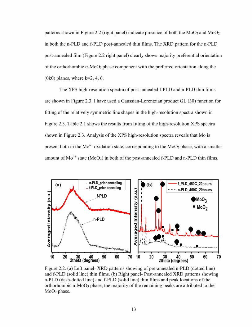
13
patterns shown in Figure 2.2 (right panel) indicate presence of both the MoO3 and MoO2
in both the n-PLD and f-PLD post-annealed thin films. The XRD pattern for the n-PLD
post-annealed film (Figure 2.2 right panel) clearly shows majority preferential orientation
of the orthorhombic α-MoO3 phase component with the preferred orientation along the
(0k0) planes, where k=2, 4, 6.
The XPS high-resolution spectra of post-annealed f-PLD and n-PLD thin films
are shown in Figure 2.3. I have used a Gaussian-Lorentzian product GL (30) function for
fitting of the relatively symmetric line shapes in the high-resolution spectra shown in
Figure 2.3. Table 2.1 shows the results from fitting of the high-resolution XPS spectra
shown in Figure 2.3. Analysis of the XPS high-resolution spectra reveals that Mo is
present both in the Mo6+ oxidation state, corresponding to the MoO3 phase, with a smaller
amount of Mo4+ state (MoO2) in both of the post-annealed f-PLD and n-PLD thin films.
Figure 2.2. (a) Left panel- XRD patterns showing of pre-annealed n-PLD (dotted line)
and f-PLD (solid line) thin films. (b) Right panel- Post-annealed XRD patterns showing
n-PLD (dash-dotted line) and f-PLD (solid line) thin films and peak locations of the
orthorhombic α-MoO3 phase; the majority of the remaining peaks are attributed to the
MoO2 phase.
10 20 30 40 50 60 70
Av
era
ge
d I
nte
ns
ity
(a
.u.)
2theta (degrees)
n-PLD_prior annealing
f-PLD_prior annealing
n-PLD
f-PLD
10 20 30 40 50 60 70
Av
era
ge
d I
nte
ns
ity
(a
.u.)
2theta (degrees)
f_PLD_450C_20hours
n-PLD_450C_20hours
MoO3
MoO2
(a) (b)

14
This somewhat of a surprising result given that no oxygen was introduced in the
growth chamber during f-PLD synthesis whereas oxygen gas was used during n-PLD
growth of molybdenum oxide thin films. I have found no evidence from my XPS spectra
of a hydroxyl component in the Mo 3d spin orbital doublet. Further XPS studies are
currently being carried out on the pre-annealed f-PLD and n-PLD films to determine
whether the annealing of the thin films under atmospheric conditions may have been
sufficient in replenishing oxygen and oxidizing Mo4+ to Mo6+.
Figure 2.4 clearly shows the change of Raman band spectrum for pre-annealed
samples vs post-annealed thin film samples. The highly amorphous nature of the pre-
annealed n-PLD film is evident in that the high range of disorder give rise to broad-
featured band in the Raman spectrum.
Figure 2.3. XPS high-resolution spectrum showing the fitted Mo 3d doublet peak for (a)
f-PLD thin film and (b) n-PLD thin film annealed at 450 °C.

15
Table 2.1. Summary of fitting results of the high-resolution XPS data representing the
Mo 3d spin orbital component peak parameters for the post-annealed f-PLD and n-PLD
thin films. The position values are in good agreement with the work of Baltrusaitis et al.
[9]. The Standard Deviation (St. Dev.) values have been estimated by performing the
Monte-Carlo simulated error analysis within the CasaXPS software.
Peak type
component-
Mo 3d
(deconvoluted)
Positio
n (eV)
FWH
M (eV)
Area %Area Position St.
Dev.
(Area St. Dev.)
f-PLD
Mo6+
(3d5/2)
232.46 1.21 2593.67 31.36 0.0041
(40.6587)
Mo4+
(3d5/2)
231.11 1.96 1614.08 19.52 0.0220
(41.7210)
Mo6+
(3d3/2)
235.59 1.25 1729.11 30.28 0.0045
(27.1058)
Mo4+
(3d3/2)
234.21 2.08 1076.05 18.84 0.0250
(27.8140)
n-PLD
Mo6+
(3d5/2)
232.49 1.73 2297.44 31.57 0.0048
(80.8277)
Mo4+
(3d5/2)
231.01 2.67 1411.21 19.39 0.0535
(46.4044)
Mo6+
(3d3/2)
235.59 1.66 1531.63 30.49 0.0078
(53.8852)
Mo4+
(3d3/2)
234.00 3.14 931.40 18.54 0.0500
(30.6269)
Conversely, the Raman spectra of the post-annealed films have distinct and
relatively sharp bands that are consistent with the presence of both MoO3 and MoO2 in
the thin films. The peaks at about 198, 224, 341, 356,452, 488, 566, 579, 732 cm-1 are

16
consistent with the MoO2 bands in the spectrum with an average Raman shift of 3 cm-1 as
compared to the study of molybdenum oxide thin films made by Camacho-Lopez et al
[10].
Figure 2.4. Raman spectra of f-PLD (solid line) and n-PLD thin films (dash-dotted line)
(a) prior- annealing & (b) post-annealing at 450 °C for upto 20 hours.
Moreover, the f-PLD sample shows Raman peaks at 664 (B3g- ν), 817 (B1g-ν)
which correspond to the Raman-active stretching modes of the bridging oxygens – OMo3
(triply-coordinated oxygen), OMo2 (doubly-coordinated oxygen) respectively and the
peak at 993 cm-1 (A1g, B1g-ν) to Mo=O (terminal oxygen bond) vibrations which results
from an unshared oxygen [2].
Conclusions
The f-PLD film show considerably more enhanced nano-structured texture vs the
n-PLD films, prior to annealing whereas both film types exhibit highly amorphous
atomic-scale structure. Oswald ripening leads to the formation of nano- to micro-sized
200 400 600 800 1000
Inte
nsit
y (
a.u
.)
Raman shift (cm-1)
n-PLD post-annealing
f-PLD post-annealing
MoO3
MoO2
200 400 600 800 1000
Inte
nsit
y (
a.u
.)
Raman shift (cm-1)
n-PLD prior annealing
f-PLD prior annealing(a) (b)

17
crystallites upon annealing in the films with a rougher morphology and smaller scale
features in the post-annealed f-PLD thin film. My XRD, XPS and Raman data show that
both the f-PLD and n-PLD result in an admixture of MoO3 and MoO2 in the thin films
after annealing. Provided that further investigations on how the femtosecond laser peak
power and short laser pulse duration affect the deposition of thin film material on various
substrates and under varying conditions, the f-PLD technique appears to be promising for
the synthesis of novel molybdenum oxide thin films.
Acknowledgements
We thank partial support from the MSU Graduate College and Rishi Patel of
JVIC for XPS measurements and US Photonics for using their facilities to prepare the f-
PLD thin films.
References
1. S. S. Kanu, R. Binions, Proc. R. Soc. A 466, 19-44 (2009).
2. G.-A. Nazri, C. Julien, Solid State Ionics 53, 376-382 (1992).
3. S.S. Sunu, E. Prabhu, V. Jayaraman, K.I. Gnanasekar, T. Gnanasekaram, Sens.
Actuators B-Chem 94, 189-196 (2003).
4. S. Balendhran , S. Walia , H. Nili , J. Z. Ou , S. Zhuiykov , R. B. Kaner , S. Sriram , M.
Bhaskaran , K. Kalantar-zadeh, Adv. Funct. Mater. 23, 3952-3970 (2013).
5. S. Amoruso, G. Ausanio, R. Bruzzese, M. Vitiello, X. Wang, Phys. Rev. B 71, 033406
(2005).
6. M. Okoshi, K. Higashikawa, M. Hanabusa, Appl. Surf. Sci. 154–155, 424–427 (2000).
18
7. M. Sanz, R. de Nalda, J.F. Marco, J.G. Izquierdo, L. Ban˜ares, M. Castillejo, J. Phys.
Chem. C 114, 4864–4868 (2010).
8. J. Perriere, E. Millon, W. Seiler, C. Boulmer-Leborgne, V. Craciun, O. Albert, J.C.
Loulergue, J. Etchepare, J. Appl. Phys. 91, 690-696 (2002).
9. J. Baltrusaitis, B. Mendoza-Sanchez, V. Fernandez, R. Veenstra, N. Dukstiene, A.
Roberts, N. Fairley, Appl. Surf. Sci. 326, 151–161 (2015).
10. M. A. Camacho-Lopez, L. Escobar-Alarcon, M. Picquart, R. Arroyo, G. Cordoba, E.
Haro-Poniatowski, Optical Materials 33, 480-484 (2011).

19
CHAPTER 3: SUBSTRATE EFFECTS ON THE STRUCTURAL AND
MORPHOLOGICAL ASPECTS OF MOLYBDENUM OXIDE THIN FILMS
SYNTHESIZED BY NANOSECOND PULSED LASER DEPOSITION
Abstract
Molybdenum oxide thin films have been synthesized using the nanosecond-based
pulsed laser deposition technique at elevated substrate temperatures resulting in the
formation of sub-stoichiometric phases (O: Mo < 3) in the annealed condition on various
substrates (glass slide, sapphire, Si wafer). The effects of type of substrate and the extent
of annealing are studied in terms of the structural, morphological and surface chemical
properties of the thin films. I find that while molybdenum oxide films deposited on both
the Si and sapphire substrates had formation of nano-crystalline features upon annealing,
the sub-stoichiometric deficiency was more pronounced in the MoOx thin film deposited
on Si substrate (MoOx/Si). The morphological and structural variations among the two
types of films may be due to the effects of wettability and strain-induced formation
mechanisms upon deposition on dissimilar crystalline substrates. These characterization
results are discussed in terms of applicability to surface related applications such as
photocatalysis.
Introduction
Molybdenum oxide has been shown to exhibit characteristics promising for
applications in the fields of photocatalysis [1], battery materials (both cathodic and
anodic [2], electrochromic devices [3], photochromic device applications [4,5] and in gas

20
sensing applications [6-8]. Binary and ternary oxides of molybdenum in combination
with other transition metals/ metal oxides, particularly when used as supported structures
on high surface area substrates of both acidic and basic nature (e.g. alumina, silica), have
the capability of working as hydrodesulphurization (HDS) catalysts [9,10]. The
orthorhombic crystal structure phase has the most favorable characteristics for the above-
mentioned applications. This is because of the layered, porous and intercalated aspects of
the structure, which enable easy diffusion for any inserted species into the intercalation
channels. However, polymorphs of this oxide, namely, a metastable β-MoO3 with a
monoclinic crystal structure, which is similar to a distorted rutile-type atomic
arrangement, also exists both in the bulk [11] as well as in nanoscale materials [12]. This
metastable structure transforms to the thermodynamically stable α-phase at temperatures
above 350 °C [12]. Additionally, several sub-stoichiometric oxides of the general
notation: MonO3n-1(where, n = 4, 5, 8, 9, 10, 17, etc.), have also been studied [13-15]. In
any of these oxygen-deficient phases, the ratio of Mo:O varies between: 2.75-2.91 [14].
The Mo4O11 sub-oxide has monoclinic(η) and orthorhombic (γ) variants, all of which
form only after a threshold of oxygen concentration is reached under equilibrium
conditions [16]. On the other hand, molybdenum dioxide (MoO2) is also a well-
established battery (anode) material having a monoclinic, distorted-rutile type structure
[17,18] and possessing metal-like properties [19]. In addition, the amorphous
molybdenum (a-MoO3) oxide thin films have some interesting photochromic properties
compared to the above mentioned crystalline phases, hence making them industry viable
components [20]. The structure and properties of molybdenum oxide based thin films can
be altered extensively by changing the parameters of deposition in chemical vapor
21
deposition (CVD) or in physical vapor deposition (PVD) [21]. Nevertheless, issues of
obtaining stoichiometric MoO3 thin films can arise from multiple effects, understanding
of the effect of deposition conditions of any specific film synthesis technique can help us
produce the desired composition, structure and properties of such transition metal oxides.
In particular, PLD has the unique capacity to produce metal oxide thin films in a reactive
gas atmosphere at low temperatures having a prescribed stoichiometry and high
crystallinity. More often than not, the nanostructured morphology of molybdenum oxides
has much better applicability and superior properties when compared to its meso-/ micro-
sized counterparts. Conversely, an accurate control of the various sub-oxides of the
molybdenum can also lead to unique and novel electrical and optical properties which
can be correlated to better photocatalytic activity [16]. Hence, the current need in terms
of parametric control in PLD technique requires a full understanding of the effect of the
substrate-thin film interaction upon deposition and under annealing conditions.
An extensive characterization study of nanosecond-laser based PLD (n-PLD)-
made molybdenum oxide thin films (MoOx) deposited on single crystal substrates (both
Si-wafer and c-plane sapphire), in terms of the structural, surface chemical and
morphology of the thin films primarily after annealing, is presented herein. The results
are explained in terms of the creation of multivalent states of Mo, and their potential
cause of origin, and the effects imposed upon by the substrate during the deposition and
during annealing of the thin films.

22
Experimental Details
The Molybdenum oxide thin films were synthesized using pulsed laser deposition
(PLD) MoO3 targets using commercially available pure MoO3 powder (99.97 %, Fischer-
Scientific). Upon finely grinding and homogeneously mixing the powder with PVA, the
material was then pressed using a 10 Metric Ton hydraulic press. The smooth, powdery
pellets that were thus formed were subsequently sintered in air at about 650 °C for at
least 12 hours in a muffle furnace. A compact and well textured orthorhombic phase
MoO3 target was confirmed using x-ray diffraction (XRD) and subsequently employed in
the PLD chamber.
Thin films were synthesized on microscopic glass slides (Corning-25 x 25 mm),
polished sides of silicon (Si) wafer (<100> n-type) substrate and c-plane (0001) sapphire
substrates, all done at elevated substrate temperature. Substrate cleaning was made in a
three-step process as follows: ultrasonic cleaning in Acetone (10 minutes), Ethyl Alcohol
rinsing and finally thoroughly rinsed in DI water and air dried. Immediate placement of
the substrates in the vacuum chamber and heating of the substrates (Ts = 300 °C) was
made in order to minimize the surface overexposure to hydroxylation. After attainment of
the desired substrate temperature under vacuum in the deposition chamber, where the
temperature was monitored using a thermocouple and controlled using a temperature
controller, the oxygen atmosphere was established to stabilize the reactive atmosphere.
The deposition chamber was consistently evacuated to an initial base vacuum of 10-5
mbar (10-3 Pa) initially and then pumped back with oxygen gas (>99%, Airgas) up to one
order magnitude increase in the chamber pressure gauge reading (10-4 mbar, or 10-2 Pa).
The laser source used for PLD was a nanosecond (ns) pulsed UV-excimer based KrF

23
laser with λ = 248 nm and pulse duration of ~ 20 ns (Lambda Physik, COMPEX201).
While an average per pulse energy of 325 mJoule was employed, an energy density/ laser
fluence of ~20 J/cm2 was achieved at the target surface. The angle between the incident
laser beam and normal to the target surface was maintained at 45°. Constant rotation of
the target carousel (10Hz) was employed to avoid local heating of the surface, hence
leading to homogenous plasma creation. With a target to substrate distance of ~6.5 cm,
the measured thin films’ thickness in the as-deposited condition on various substrates
varied between 40 – 50 nm. All of the thickness measurements were performed ex-situ
using a Veeco Dektak 150 surface profilometer, and the measurement/data analysis
methods of which are discussed in the ensuing Supplementary Information section(SI).
The scanning electron microscopy (SEM) imaging and complementary energy-
dispersive x-ray spectroscopy (EDX) analysis were performed on specimens of the thin
films as deposited on the substrates, which were affixed to either carbon (C) or copper
(Cu) tape. The SEM and EDX analyses were performed at various film locations using
horizontal and tilted stage modes. For this purpose, a FEI Quanta 200 SEM instrument
was employed with operating voltage of 5-20kV and an Oxford Instruments INCA EDX
detector was utilized for elemental analysis. In addition to the SEM analysis, imaging of
the surface morphology of the films was also made using an Atomic Force Microscope
(Bruker-Dimension Icon). The single crystal (n-doped) silicon AFM probe with a radius
~8 nm (spring constant: 48 N/m and resonant frequency: 190 KHz) were used in tapping
mode for these studies. The AFM data were processed using the Bruker NanoScope
Analysis Suite 1.30.
24
Ambient temperature X-ray diffraction (XRD) measurements were performed on
the thin films for structural and phase determination in both as-deposited and post-
annealed conditions using a Cu-Kα radiation X-ray source (Bruker D8 Discover) with
λ=1.54184 Å. The instrument parameters for the X-ray source were consistently set at
40kV accelerating voltage and 40 mA of electron current. A Gobel mirror was employed
in the incident side and 0.6mm slit were used for both primary and secondary divergence
slits.
The X-ray Photoelectron spectroscopy (XPS) technique was made using a twin-
crystal monochromatic Al-Kα source with characteristic energy of 1486.6 eV. A Thermo
Scientific Alpha 100 hemispherical Constant Analyzer Energy analyzer (CAE) with 25
eV pass energy was employed for data acquisition. The Ag 3d5/2 (FWHM=0.36 eV) peak
with a characteristic energy of 368.26 eV was used for calibration of the Instrument
source and analyzer. Data analysis and spectral peak deconvolution was performed using
CasaXPS 2.3.16 software package, with the Marquardt–Levenberg optimization
algorithm. Data calibration was performed using an internal standard-based C1s peak
position referenced at binding energy (BE) 284.8 eV. A Shirley background was used for
all the spectroscopic regions analyzed. Additionally, a choice of line shape between a
Gaussian- Lonrentzian product, GL (30) and a Lorentzian asymmetric functional form
convoluted with a Gaussian function, LA(a,b,n) was made for both the survey and high-
resolution spectra. The vibrational phonon modes were determined by using a vertically
polarizable green laser, λ=532 nm (Horiba LabRAM HR) based micro-Raman
spectrometer having an instrumental resolution of ~1 cm-1 with variable optical density
25
filters. The Raman data was acquired and analyzed for peak deconvolution and fitting
using Labspec 5 software.
Results and Discussion
It was pointed out that a variation of thermal and lattice mismatch is possible
among thin films grown on different substrates, based on their respective thermal
expansion coefficients and preferred orientation [22]. This in turn affects the thin film’s
morphology and crystal structure. Moreover, the as-deposited thin films on glass were
observed to be light blue in color, which transformed as the thermal treatment was
proceeding through various color stages as follows: dark bluish followed by foggy white
and finally more transparent at the selected annealing temperature (450 °C). These color
transitions, which are indicative in amorphous molybdenum oxide thin films, were also
observed by others in their annealing studies [23]. Numerous studies have reported on the
effect of oxygen partial pressure (PO2) and substrate temperature (Ts) on the
stoichiometry and phase purity using related techniques, such as PVD or sputtering [24,
25]. It has been reported that in-situ thermal annealing by use of the heated substrate has
a pronounced effect on the extent of crystallinity of the as-deposited thin films [21]. In
addition, the chamber pressure directly affects the grain size of the thin films during
deposition [26]. Moreover, the thermal annealing of the post-deposited thin films
typically produces more crystalline films and larger crystalline grain size, due to thermal
activated atomic diffusion and Ostwald ripening, respectively. The enhanced diffusion
and greater tendency of the atoms to organize in crystalline arrangements also leads to
more enhanced atom-to-atom interactions with crystalline substrates at higher annealing
26
temperatures [27]. XRD analysis of the as-deposited thin films on all three types of
substrates shows these to be highly predominantly amorphous in nature (see, for example,
Figure 2.1a in Chapter 2 and in the Supplementary Information (SI) section.
The change from amorphous to crystalline nature is likely dependent on the
thickness of the thin films. The SEM images and film thickness measurements show
evidence of non-uniform thickness in all of the thin films synthesized for this study. As
discussed below, the non-uniformity appears to be of importance in the inhomogeneity of
the crystalline regions upon annealing of the thin films.
For the film deposited on the Si substrate (MoOx/Si thin film) at a substrate
temperature (Ts) of 300 °C after ex-situ annealing at 450 °C for 6 hours, as shown in Fig.
3.1(a), the development of granular texture was obtained in some regions owing to the
crystalline rearrangement during thermal treatment. This is consistent with the XRD
results (shown below) showing that an orthorhombic structure has developed along with
an amorphous component in the MoOx/Si thin film Interestingly, there were additional
regions with micro-nano crystallites observed in the SEM images, (width < < 1 μm;
several microns in length) having faceted features. A folded-like texture was also
predominant in major areas of the post-annealed thin films. Interestingly, there were
some regions consisting of mixed amorphous/crystalline phases, which could be best
described as crystalline phases embedded in an amorphous matrix. In addition, there were
also regions of different grain shapes ranging from needle-like to ellipsoidal, including
elongated columns. The resulting morphology may be due to an insufficient annealing
time (6 hours) provided for the larger areas of the thin film’s surface. On the other hand,
the formation of molybdenum oxide(s) having this varied morphology in the MoOx/Si

27
thin film, which suggests presence of primary and secondary phases, may also result from
the annealing process. In addition, the effects due to ionizing radiation causing material
change and modification cannot be fully discounted. Earlier reports have shown evidence
of partial transformation of the MoO3 to MoO2 through ion bombardment upon major
irradiation from X-rays or electrons, which are present in any characterization study vis-
à-vis SEM, XRD, XPS [28].
Attempts at scraping of the thin films showed a high level of adhesion for the as-
deposited MoOx/Si thin film. This is most likely due to the formation of covalent bonding
between the MoOx thin film and the Si/SiO2 substrate. Apart from this, an observation
from the morphology that may reflect upon the crystallite growth or deposition
mechanisms is worth mentioning. I observed circular-shaped predominantly amorphous
regions containing some segregated crystallites with globular-type craters in the middle.
Lopez et al observed similar distinguishable annular craters in their laser-induced
structural transformation study of molybdenum oxides [19].
The SEM images of the post-annealed thin film (450 °C-6 hours) deposited on
sapphire substrates (Fig. 3.1 (c, d)) show a much more uniform coverage than the film
deposited on Si. This suggests a higher wettability of the film deposited on sapphire
(MoOx/sapphire) compared to the film deposited on Si. I conjecture that this greater
wettability may be associated with a tendency of the crystallites of the thin film to form
epitaxial registry, although with considerable lattice mismatch, with the sapphire
substrate. This is consistent with several features observed in the post-annealed thin film,
such as ruptures and micro cracks that developed in dendritic-like pattern. SEM imaging
of the regions containing the micro-cracks proved to be difficult due to substantial

28
charging effects associated with the sapphire-exposed areas. The lower wetting
mechanism of the thin film on the Si substrate, which results in a large contact angle
between the film and substrate, is also consistent with the formation of globule-like
regions and in the greater tendency of retaining semi-crystalline or mixed
amorphous/crystalline character upon annealing.
Fig. 3.1. SEM micrograph of MoOx thin films deposited on the Si substrate (a & b), and
sapphire substrate (c & d), both annealed at 450 °C for 6 hours (at various
magnifications).
Because of the incomplete transformation of the amorphous regions when
compared to post-annealed thin film on the sapphire substrate, another annealing cycle
was performed on the MoOx/Si thin film for an additional 6 hours. SEM images of the
(a)
1 μm
(c) (d)
(b)
5 μm
4 μm 5 μm

29
thin film exposed to the second annealing cycle revealed excellent terraced- crystallites
(Fig. 3.2 (a)), owing to the additional nucleation and growth due to Ostwald ripening. The
morphology of tabular, elongated crystallites is consistent with the orthorhombic phase-
type growth of MoO3 (see Fig. 3.2 (a, b)). In all, there was an admixture of crystalline
orthorhombic-like phases with an amorphous moiety extending throughout the film. In
addition, there are smaller more roundish nanoscale features, which are consistent with
additional thermodynamically stable MoOx phases: As shown in the following
discussions, this is consistent with the XRD characterization of the thin films.
Fig. 3.2. (a) SEM image of MoOx/Si thin films after annealing for a total of 12 hours,
shows development of terrace-like features on a large scale (the inset is of a tilted scan
close-up image (tilt angle-30°) justifying the clear faceting aspect in a step-like nature, 2
μm scale). (b) some regions also possessed highly strained, rod-like feature in
combination with the faceted planes.
Almost all of the post-annealed samples varied considerably in appearance (see
SI) with respect to their as-deposited counterparts, in the sense that they had a foggy,
translucent character, which might be related to their larger grain size. Comparatively, the
(a) (b)
1 μm 5 μm

30
MoOx thin film deposited on sapphire had more densely packed nanograins than the
molybdenum oxide film deposited on the Si substrate.
After extensive annealing (for 20 hours at 450 °C) of the molybdenum oxide thin
film deposited on the glass substrate (MoOx/glass; Ts = RT), SEM images (see Fig. 3.3)
revealed the growth of slabs of nano- to micrometer-extent having nanometer thickness,
stacked along their rectangular regions forming a series of cascades. This behavior was
also nominally observed in the molybdenum oxide thin film deposited on Si. Extreme
faceting of the larger areas was observed owing to the anisotropic growth during longer
annealing times (20 hours) on the MoOx/glass thin film.
Fig. 3.3. SEM micrograph of post-annealed thin film (for 20 hours) deposited on the glass
substrate (n-PLD, Ts=RT).
The AFM imaging has been very useful for providing information on the aspect
ratio of the thin film samples along with textural information in terms of the film surface
roughness (Rrms). As it is clearly evident from Fig. 3.4, the post-annealed thin film
deposited on the Si substrate has more elongated nanocrystals along with a wider range of
10 μm

31
crystallite sizes (starting from at least ~70 nm) than the post-annealed MoOx/sapphire
thin film.
Fig. 3.4. AFM 3D images of post-annealed samples of MoOx thin films on: sapphire
substrate (left) with the depth (z-axis) of 41.1 nm and Si substrate (right) with the depth
(z-axis) of 81.4 nm. The scale bar in the xy-plane is 2 μm x 2 μm.
Moreover, when viewed in combination with the SEM micrographs shown earlier
(Fig. 3.1 and Fig. 3.2), it can be surmised that the thin film deposited on Si favors the
creation of a multilayered morphology; however, the multilayering is considerably more
pronounced in the MoOx/glass thin film.
A more densely packed grainy texture is observed in thin film deposited on
sapphire in comparison to the one deposited on Si, from the nanometer-scale particle
analysis of the AFM 2D image (Fig. 3.5 (a, b)). If observed carefully, there were
interference hues throughout the 2D image of MoOx/Si (Fig. 3.5 (b)). This might be due
the semiconducting nature of the substrate. The roughness factors (Rq), which are
calculated using AFM 2D micrograph analysis are ~13 nm for MoOx/sapphire in
comparison to the ~23.2 nm for the one deposited on Si (MoOx/Si). Thus, the Rq for

32
MoOx/Si thin film is ~76% higher than that of MoOx/sapphire thin film, despite the Si-
substrate being considerably smoother than the sapphire substrate. This effect has been
explained by Illyaskutty et al [22], who claim that smoother substrates have lower
adhesion irrespective of the nature of the film-substrate bonding mechanism (Van der
Waals attractions, Chemisorption etc.).
Fig. 3.5. AFM 2D images (2 μm x 2 μm) of post- annealed thin film samples of MoOx
deposited on (a) sapphire substrate (b) Si substrate.
The variation of average d-spacing suggests a less perfectly ordered system at the
atomic scale whereas a fewer number of reflections/peaks in an XRD pattern is
suggestive of preferential orientation of the thin film on a substrate. The preferential
orientation of the nano- to micro-crystalline grains was present in both films as confirmed
through phi and chi scans performed with the diffractometer. It was noted above that thin
film XRD data analysis can be more challenging when compared to powder diffraction,
due to preferred orientation issues in thin films which causes some of the peaks to absent
from the XRD pattern.
(a) (b)

33
In the analysis of the XRD data, the effects due to potential epitaxial type registry
of film to substrate needs to be borne in mind. A simple calculation of epitaxial mismatch
(% l) of the thin films with respect to their substrates, can be performed as follows,
𝑙 = [𝑎𝑠 − 𝑎𝑓
𝑎𝑓 ∗ 100] %
where, as and af are the unstrained lattice parameters of the substrates and the respective
thin films, i.e. in their intrinsic state [22]. This attempt at epitaxial preference forces the
film’s crystal lattice to undergo a strain, which would in general be relaxed during a
thermal treatment process. It should be noted that, despite the extent of epitaxial
mismatch of the MoO3 crystal lattice with the sapphire substrate being much less when
compared to the silicon substrate, the residual stress/strain produced would not be the
driving mechanism for any potential oxygen vacancy formation. As was mentioned
above, the scraping tests performed on the as-deposited samples showed strong adhesion
of the film on the sapphire substrate, partly owing to the atomic interlocking of the MoOx
crystal lattice with respect to the sapphire lattice in the c-plane, and partly due to the
higher degree of wettability of the MoOx/Al2O3 interface.
Added to this, the effect of thermal conductivity and thermal expansion
coefficients can also significantly override the natural growth of thin film on these
substrates. For example, as per the work of Illyaskutty et al [22], since the thermal
conductivity of Si is more than 200% greater than that of sapphire substrate, this
substantially impacts grain growth propagation throughout the substrate surface when
uniformly heated during annealing. Coincidentally, the effect due to this thermal
conductivity difference has been observed in the morphological differences of the thin
films, i.e., MoOx/Si shows elongated layered structures, which is related to the enhanced

34
thermal conductivity of Si. At the same time, the sapphire substrate, despite being more
epitaxially suitable, provides lower mobility for the growing crystallites, hence
hampering the creation of the desired morphology during annealing.
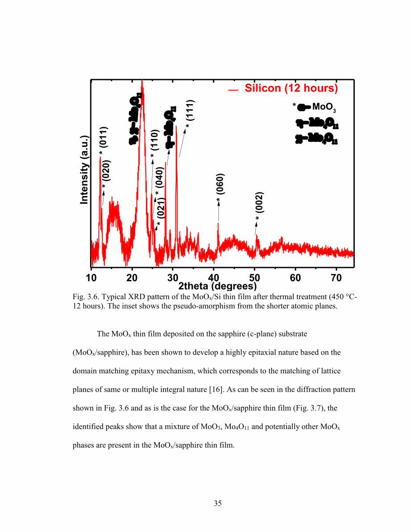
Upon analysis of the MoOx/Si thin film XRD pattern shown in Fig. 3.6, I find
evidence for a pseudo-amorphous component from the peak centered at ~16° and a -
and/or -Mo4O11 component in the thin film: Note that the background, which shows
additional evidence of an amorphous component, has been partially removed from the
XRD pattern. The Mo4O11 phase has a dimension that is particularly small in the
nanoscale, as evidenced from the peak at 22.64°. This is due to the extreme variation in
the confinement aspect of the scattered X-rays in the diffraction experiment being very
small for one set of planes versus the preferentially oriented planes of the elongated nano-
crystallites, which in turn causes broader than usual peaks based on the Scherrer
relationship of FWHM and the crystallite size. Thus, it is evident that a mixture of MoO3,
Mo4O11 and potentially other MoOx phases persist in the thin film deposited on the Si
substrate. Moreover, XRD measurement of molybdenum oxide structures on Si-based
supports is very challenging because of the high intensity of the Si peak coinciding with
the 2θ positons of molybdenum oxide phases. The solution for this is by employment of
chi angle and phi angle scans. This allows for the reduction of the single crystal silicon’s
intense peak, and simultaneously improving the count statistics for measurement of the
thin film’s diffraction pattern. The precise determination of the amorphous component of
the thin film on Si substrates, say by use of Rietveld refinement, is complicated due to an
amorphous SiO2 or SiO oxide layer on Si [29]. It is because of such complexities that I
chose not to perform Rietveld refinement of the XRD data measured from the thin films.
35
Fig. 3.6. Typical XRD pattern of the MoOx/Si thin film after thermal treatment (450 °C-
12 hours). The inset shows the pseudo-amorphism from the shorter atomic planes.
The MoOx thin film deposited on the sapphire (c-plane) substrate
(MoOx/sapphire), has been shown to develop a highly epitaxial nature based on the
domain matching epitaxy mechanism, which corresponds to the matching of lattice
planes of same or multiple integral nature [16]. As can be seen in the diffraction pattern
shown in Fig. 3.6 and as is the case for the MoOx/sapphire thin film (Fig. 3.7), the
identified peaks show that a mixture of MoO3, Mo4O11 and potentially other MoOx
phases are present in the MoOx/sapphire thin film.
10 20 30 40 50 60 70
* (1
11)
* (0
20)
* (0
02)
* (0
60)
* (0
40)
* (0
11)
* (1
10)
Silicon (12 hours)In
ten
sit
y (
a.u
.)
2theta (degrees)
* MoO3
* (0
21)

36
Moreover, the MoOx/sapphire thin film exhibits d-spacing shifted to slightly
lower 2 values in relation to that of the MoOx/Si thin film. It is plausible that this is due
to the epitaxial mismatch difference being considerably lower for MoOx vs sapphire than
of MoOx vs Si, for their respective lattice plane orientations at the thin film-substrate
interface.
Fig. 3.7. XRD pattern of the MoOx/sapphire thin film after thermal treatment (450 °C-6
hours).
The chemical states of the thin film surfaces were probed using XPS, both
through survey spectrum and high-resolution (HR) scan analysis. The XPS spectra
collected from the MoOx/sapphire thin film showed evidence for hydroxide formation
most likely due to a nominal hydroxylation of the sapphire surface’s dangling bonds at
10 20 30 40 50 60 70
* MoO3
* (0
02)
* (0
60)
* (0
21)
Sapphire substrate MoOx (6hours)
Inte
ns
ity
(a
.u.)
2theta (degrees)
* (0
11) * (1
11)
* (1
10)
37
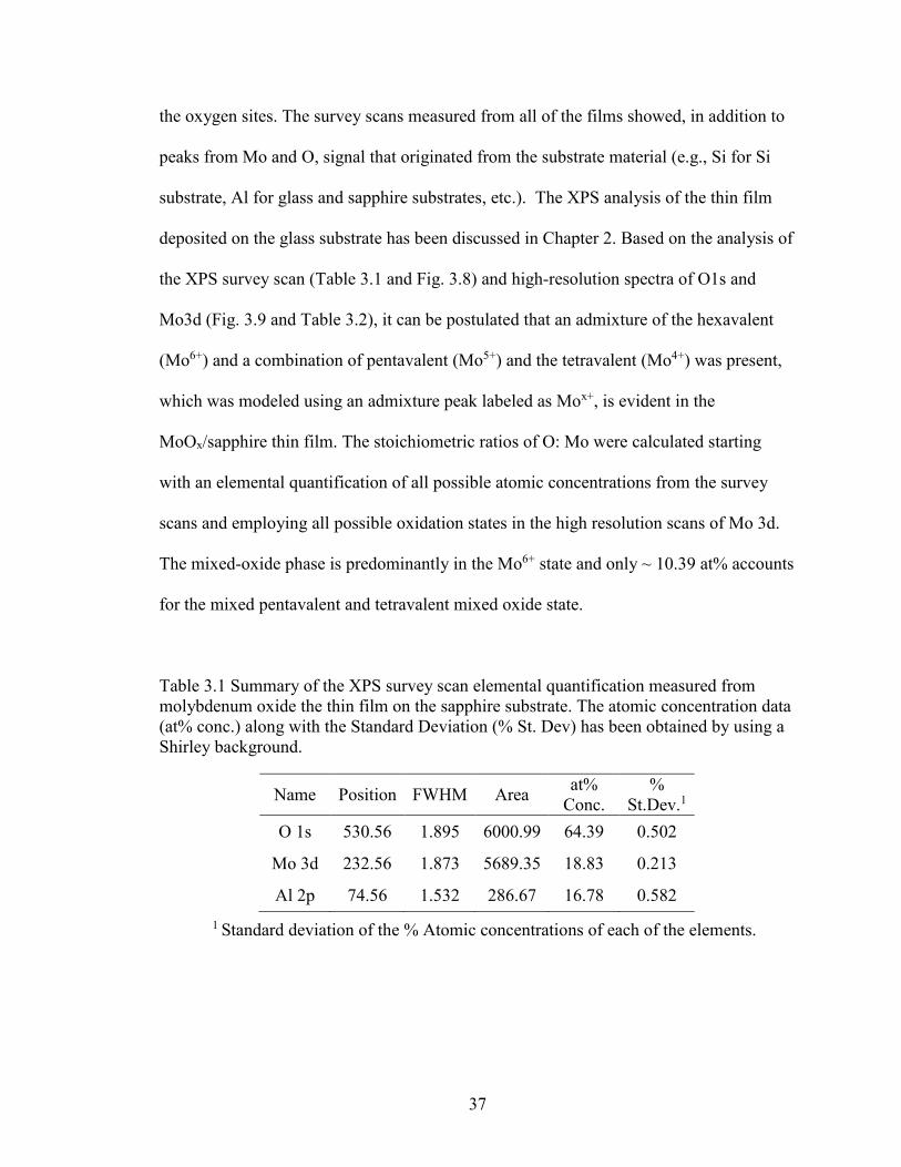
the oxygen sites. The survey scans measured from all of the films showed, in addition to
peaks from Mo and O, signal that originated from the substrate material (e.g., Si for Si
substrate, Al for glass and sapphire substrates, etc.). The XPS analysis of the thin film
deposited on the glass substrate has been discussed in Chapter 2. Based on the analysis of
the XPS survey scan (Table 3.1 and Fig. 3.8) and high-resolution spectra of O1s and
Mo3d (Fig. 3.9 and Table 3.2), it can be postulated that an admixture of the hexavalent
(Mo6+) and a combination of pentavalent (Mo5+) and the tetravalent (Mo4+) was present,
which was modeled using an admixture peak labeled as Mox+, is evident in the
MoOx/sapphire thin film. The stoichiometric ratios of O: Mo were calculated starting
with an elemental quantification of all possible atomic concentrations from the survey
scans and employing all possible oxidation states in the high resolution scans of Mo 3d.
The mixed-oxide phase is predominantly in the Mo6+ state and only ~ 10.39 at% accounts
for the mixed pentavalent and tetravalent mixed oxide state.
Table 3.1 Summary of the XPS survey scan elemental quantification measured from
molybdenum oxide the thin film on the sapphire substrate. The atomic concentration data
(at% conc.) along with the Standard Deviation (% St. Dev) has been obtained by using a
Shirley background.
1 Standard deviation of the % Atomic concentrations of each of the elements.
Name Position FWHM Area at%
Conc.
%
St.Dev.1
O 1s 530.56 1.895 6000.99 64.39 0.502
Mo 3d 232.56 1.873 5689.35 18.83 0.213
Al 2p 74.56 1.532 286.67 16.78 0.582

38
Fig. 3.8. The survey scans of thin films on both the substrates: sapphire (Black-Top) and
Si (Red-Bottom) showing the presence of only the constituent elements present in the
thin films (Mo, O) and substrates (Al from sapphire; Si from silicon substrate).
Moreover, it has been pointed out that these sub-oxides possess the largest values
of FWHM among all possible oxides of molybdenum, partly owing to the reason that
there were at least 7 noted sub-stoichiometric oxides of varied MoOx phases [15]. Upon
calculating the elemental at% concentrations from the survey scans, and accounting for
the Al-O (Al2O3) bond component in the O1s HR spectrum, it was concluded that the
relative O: Mo was ~2.9. The accurate estimation of all the sub-oxides along with their
atomic concentrations would warrant a higher spectral resolution in the HR scans, which
was a serious limitation to this experimental procedure, even after optimization of the
fitting parameters. The results from fitting of the high-resolution spectra of the Mo 3d
1400 1200 1000 800 600 400 200 0O
1s
O K
LL
C K
LL C
1s
Inte
ns
ity
(a
.u.)
Binding Energy (eV)
Sapphire
SiO2/Si
C K
LL
O K
LL
O 1
s
Mo
3p
1/2
Mo
3p
3/2
Mo
3d
Al 2s
Al 2p
Si 2s
Si 2p
Mo
3d
C 1
s
Mo
3p
1/2
Mo
3p
3/2

39
and O1s regions were found to be in conformance within my constraint method (Fig.
3.9).
Fig. 3.9. The high-resolution (HR) spectra fitting of MoOx/sapphire thin film showing
O1s (left) and Mo3d (right) components. The fitting parameters and constraints are partly
based on the output from the survey scan regarding the possible components and their
corresponding peak positions. The fitting summary is detailed in Table 4.1.
While the HR XPS spectra measured from the MoOx/Si thin film did not have any
major charging features, which is reasonable based on the semi-conducting nature of Si,
there was a significant distortion in peak shape of O1s HR spectrum. As shown in Fig.
3.10, the lower binding energy (BE) feature is due to the Mo-O bonding in a multivalent
state, while the Si-O contribution, due to a few monolayer thickness of SiO2 on the
surface of Si, occupies the major portion of the area of the HR spectrum. There are
different possible explanations for this peculiar behavior.
534 532 530 528
Inte
ns
ity
(a
.u)
Binding Energy (eV)
Experimental
Mo6+-O
Mox+-O
Sapphire
Fit
O1s
238 236 234 232 230
Mo3d
Inte
ns
ity
(a
.u)
Binding Energy (eV)
Experimental
Mo 3d5/26+
Mo 3d3/26+
Mo 3d5/2x+
Mo 3d3/2x+
Fit
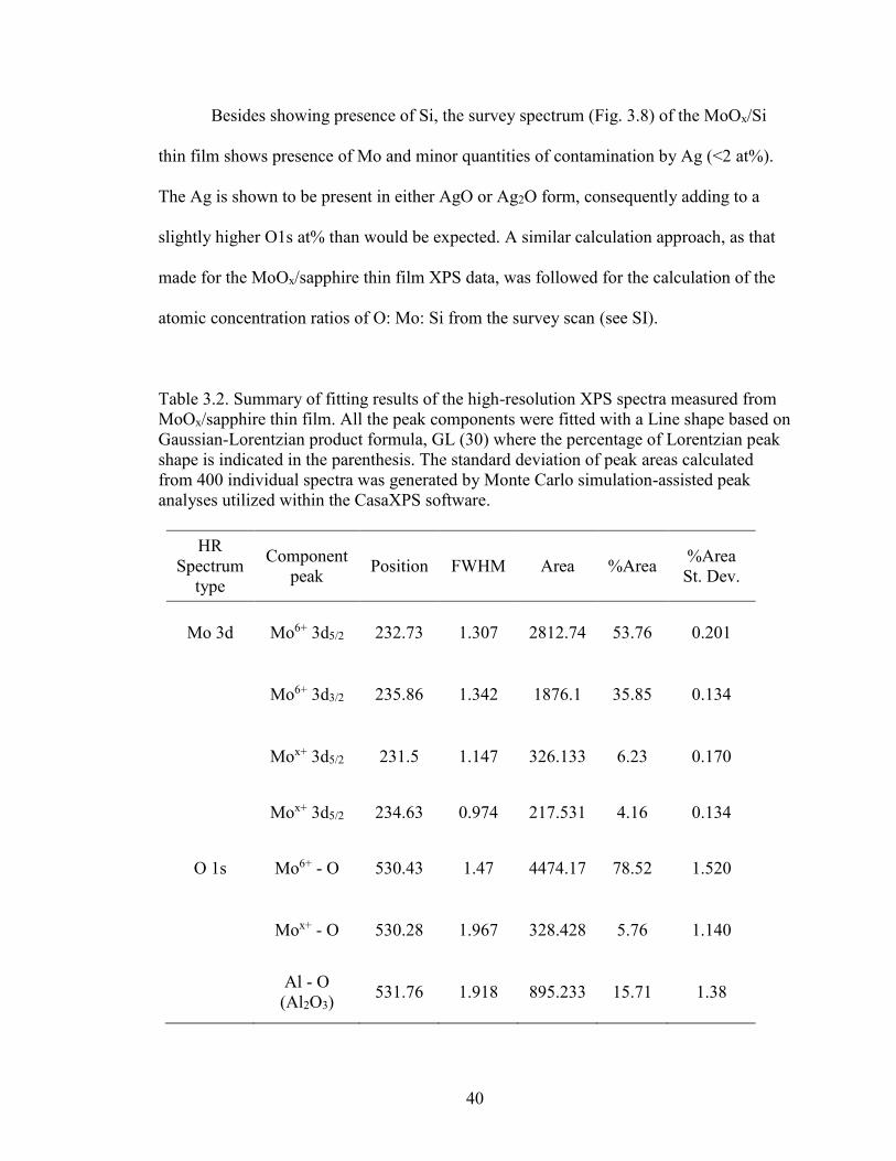
40
Besides showing presence of Si, the survey spectrum (Fig. 3.8) of the MoOx/Si
thin film shows presence of Mo and minor quantities of contamination by Ag (<2 at%).
The Ag is shown to be present in either AgO or Ag2O form, consequently adding to a
slightly higher O1s at% than would be expected. A similar calculation approach, as that
made for the MoOx/sapphire thin film XPS data, was followed for the calculation of the
atomic concentration ratios of O: Mo: Si from the survey scan (see SI).
Table 3.2. Summary of fitting results of the high-resolution XPS spectra measured from
MoOx/sapphire thin film. All the peak components were fitted with a Line shape based on
Gaussian-Lorentzian product formula, GL (30) where the percentage of Lorentzian peak
shape is indicated in the parenthesis. The standard deviation of peak areas calculated
from 400 individual spectra was generated by Monte Carlo simulation-assisted peak
analyses utilized within the CasaXPS software.
HR
Spectrum
type
Component
peak Position FWHM Area %Area
%Area
St. Dev.
Mo 3d Mo6+ 3d5/2 232.73 1.307 2812.74 53.76 0.201
Mo6+ 3d3/2 235.86 1.342 1876.1 35.85 0.134
Mox+ 3d5/2 231.5 1.147 326.133 6.23 0.170
Mox+ 3d5/2 234.63 0.974 217.531 4.16 0.134
O 1s Mo6+ - O 530.43 1.47 4474.17 78.52 1.520
Mox+ - O 530.28 1.967 328.428 5.76 1.140
Al - O
(Al2O3) 531.76 1.918 895.233 15.71 1.38
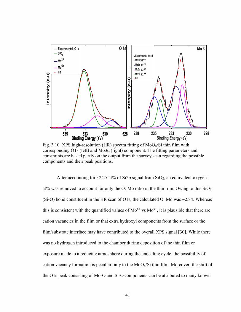
41
Fig. 3.10. XPS high-resolution (HR) spectra fitting of MoOx/Si thin film with
corresponding O1s (left) and Mo3d (right) component. The fitting parameters and
constraints are based partly on the output from the survey scan regarding the possible
components and their peak positions.
After accounting for ~24.5 at% of Si2p signal from SiO2, an equivalent oxygen
at% was removed to account for only the O: Mo ratio in the thin film. Owing to this SiO2
(Si-O) bond constituent in the HR scan of O1s, the calculated O: Mo was ~2.84. Whereas
this is consistent with the quantified values of Mo6+ vs Mox+, it is plausible that there are
cation vacancies in the film or that extra hydroxyl components from the surface or the
film/substrate interface may have contributed to the overall XPS signal [30]. While there
was no hydrogen introduced to the chamber during deposition of the thin film or
exposure made to a reducing atmosphere during the annealing cycle, the possibility of
cation vacancy formation is peculiar only to the MoOx/Si thin film. Moreover, the shift of
the O1s peak consisting of Mo-O and Si-O components can be attributed to many known
238 235 233 230 228In
te
ns
ity
(a
.u)
Binding Energy (eV)
Experimental-Mo3d
Mo3d5/2 6+
Mo3d 3/2 6+
Mo3d 5/2 x+
Mo3d 3/2 x+
Fit
Mo 3d
535 533 530 528
O 1sIn
te
ns
ity
(a
.u)
Binding Energy (eV)
Experimental- O1s
SiO2
Mox+
Mo6+
Fit

42
physical phenomenon like extra-atomic relaxation due to higher amount of defects or
local charging effect of the insulating type of thin film [31].
Based on the analysis of the Raman spectra shown in Fig. 3.11 (the identified
Raman modes are tabulated in Table 3.3), the spectral features present in the 900–600
cm−1 and 400–200 cm−1 regions are due to the Mo–O stretching and bending modes,
respectively, which are evident in both thin films. However, the peaks located in regions
< 200 cm-1 stem from lattice modes within the crystalline phases [14]. The Raman
spectrum of the annealed MoOx thin film deposited on glass has been discussed in
Chapter 2.
Fig. 3.11. Raman spectra (in the 50-1050 cm-1 range) of MoOx thin film deposited on
SiO2/Si (Top-Red) and on the sapphire substrate (Bottom-Black), both at Ts = 300 °C,
after post-annealing at 450 °C for 12 hours and 6 hours respectively. The high intensity
Si single crystal Raman band (~520.7 cm-1) has been cut-off for easier display of the thin
film modes. The band positions of various vibrational modes in the MoOx have been
noted (blue).
200 400 600 800 1000
37833
7290
244
194
158
127
Inte
nsit
y (a
.u.)
Raman Shift (cm-1)
Silicon (#)
Sapphire (*)
*
**
*
*
665
818
995
#
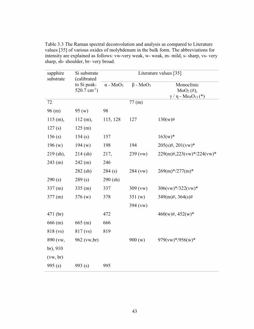
43
Table 3.3 The Raman spectral deconvolution and analysis as compared to Literature
values [35] of various oxides of molybdenum in the bulk form. The abbreviations for
intensity are explained as follows: vw-very weak, w- weak, m- mild, s- sharp, vs- very
sharp, sh- shoulder, br- very broad.
sapphire
substrate
Si substrate
(calibrated
to Si peak-
520.7 cm-1)
Literature values [35]
α - MoO3 β - MoO3 Monoclinic
MoO2 (#),
γ / η - Mo4O11 (*)
72 77 (m)
96 (m) 95 (w) 98
115 (m),
127 (s)
112 (m),
125 (m)
115, 128 127 130(w)#
156 (s) 154 (s) 157 163(w)*
196 (w) 194 (w) 198 194 205(s)#, 201(vw)*
219 (sh),
243 (m)
214 (sh)
242 (m)
217,
246
239 (vw) 229(m)#,223(vw)*/224(vw)*
290 (s)
282 (sh)
289 (s)
284 (s)
290 (sh)
284 (vw) 269(m)*/277(m)*
337 (m) 335 (m) 337 309 (vw) 306(vw)*/322(vw)*
377 (m) 376 (w) 378 351 (w)
394 (vw)
349(m)#, 364(s)#
471 (br) 472 460(w)#, 452(w)*
666 (m) 665 (m) 666
818 (vs) 817 (vs) 819
890 (vw,
br), 910
(vw, br)
962 (vw,br) 900 (w) 979(vw)*/956(w)*
995 (s) 993 (s) 995

44
It is generally established that, the intense sharp peak at about 819 cm -1 (Fig.
3.11) is due to the doubly coordinated oxygen (O-Mo2) stretching mode, which is a
consequence of corner-sharing oxygens within the octahedral MoO6 units having
alternating bond lengths [14]. In addition, the peak at 666 cm-1 is assigned to the triply
coordinated oxygen (O-Mo3) stretching mode, which is due to the edge-sharing oxygens
in common with three adjacently placed octahedral units. While the peak located at 995
cm-1 is attributed to the terminal oxygen (Mo=O) stretching mode along the a-axis and b
direction within the layered orthorhombic structure of MoO3.
As shown in Table 3.3, the band positions obtained in this work are highly
consistent with the reported values. In the bending modes region, the peaks at 290 and
337 + 377 cm-1 are consistent with the known O-Mo-O scissoring and O=Mo=O wagging
modes, respectively [32]. I have also identified Raman band features of α-Al2O3
(corundum) that are present in the MoOx/sapphire thin film. The Raman peaks located at
377, 417, 428, 447, 576, 749 cm-1 are most likely associated with the 2A1g + 5 Eg active
phonon modes of the D63d symmetry corundum space group [33, 34]. It can be noted that
both the MoOx/sapphire and the MoOx/Si thin film (annealed for 12 hours) have very
similar features apart from a redshift of ~1-3 cm-1, which is most likely due to
miscalibration issues.
None of the Raman bands that are consistent with known reported values of
MoO2 were identified. This may indicate a negligible MoO2 content or it may reflect a
much lower cross section of excitation of Raman modes associated with this phase [35].
The hint of other sub-stoichiometric molybdenum oxides (e.g., Mo4O11) is indicated in
the broader peaked features at the [835-845 cm-1, 906-911 cm-1] band positions,

45
especially in the MoOx/sapphire case. The low Raman scattering efficiency and the
increased Rayleigh scattering below 400 cm-1, of these reduced molybdenum oxides
makes determination of such modes in Raman spectra difficult [35].
The relatively broad Raman features located in the frequency range that is
consistent with mode associated with MoOx sub-stoichiometric oxides may be due to
increased structural disorder or relatively close and overlapping bands of these phases.
Indeed, as was noted above, the total spectral information of Mo4O11 is a superposition of
Raman bands of corner-shared octahedral units of β–MoO3 and the Mo4+ (tetravalent)-
centered units present in MoO2. Hence, the evidence for the presence of Mo4O11 phase,
although not entirely direct, from the Raman spectra is quite suggestive. Moreover, the
feature is slightly shifted (at 72 cm-1) is quite consistent with the presence of β -MoO3 in
the MoOx/sapphire thin film, especially since this phase is an excellent Raman scatterer
(see Table 3.3).
Finally, I discuss the defects in these thin films that have been detected using
Raman spectroscopy. In the case of the sapphire substrate, the possibility of formation of
aluminum trimolybdates (Al2(MoO4)3) in the MoOx thin film is evident with broad peak-
like features at 1006 cm-1 and 380 cm-1 frequency values [36]. However, due to the fact
that the intensity is quite low for these bands, which suggests that the content of
aluminum trimolybdates may be quite low.
It has been shown that lattice oxygen defects play a major role in the selective
catalysis processes [32]: The redox processes of Mo oxides are dependent on oxygen
vacancies and synthesis process are designed to ensure their nominal content on the
surface of these materials. The evidence of Mo5+ present in the MoOx/sapphire and

46
MoOx/Si thin films implies that there are oxygen vacancies located at the surface regions
of the films. This, coupled with a sizable component of nanoscale morphological features
inherent in the annealed thin films, makes these materials potentially suitable for
selective catalytic applications.
Conclusions
My SEM and AFM results show that upon annealing at 450 °C, the MoOx/Si thin
film has a noticeably greater roughness (by 76%) than the MoOx/sapphire thin film. In
addition, the MoOx/Si thin film had to be annealed for approximately twice the duration
(~12 hours) in order to achieve a similar level of crystallinity as the MoOx/sapphire thin
film (annealed for ~ 6 hours). This may have been driven in part by the wetting
characteristics of the MoOx thin film on the two types of substrates: the wettability of
molybdenum oxide on sapphire (c-axis) is greater than for Si(100). The SEM and AFM
images showed the surface morphology to be considerable more uniform for the post-
annealed MoOx/sapphire thin film than for the MoOx/Si thin film. My XRD, XPS and
Raman analyses confirmed the presence of MoO3, Mo4O11, and very likely additional
sub-stoichiometric molybdenum oxide phases, although the confirmation of the latter
could not be made with complete certainty. The most plausible explanation for the mixed
phases is that while there was an oxygen partial pressure established in the high vacuum
deposition chamber during thin film synthesis, it was at a level that enabled deposition of
stoichiometric and sub-stoichiometric molybdenum oxide phases in the thin films.
47
Acknowledgements
The Author would like to thank Rishi Patel of the JVIC center at MSU for making
the XPS measurements and AFM imaging on all the samples. Financial support has been
provided partially by Graduate College at MSU.
References
[1]M. Anpo, T.S.T. Suzuki, Y. Kubokawa, F. Tanaka, S. Yamashita, Photoluminescence
Evidence for the Influence of Symmetry of Molybdenum Ions upon Photocatalytic
Activity, J. Phys. Chem. 88 (1984) 5778-5779.
[2]S. Hariharan, K. Saravanan, P. Balaya, α-MoO3: A high performance anode material
for sodium-ion batteries, Electrochem. Communications 31 (2013) 5–9.
[3]C.S. Hsu, C.C. Chan, H.T. Huang, C.H. Peng, W.C. Hsu, Electrochromic properties of
nanocrystalline MoO3 thin films, Thin Solid Films 516 (2008) 4839–4844.
[4]C.G. Granqvist, Handbook of Inorganic Electrochromic Materials, first ed., Elsevier,
Amsterdam 1995.
[5]T. He, J. Yao, Photochromism of molybdenum oxide, J. Photochem. and Photobiol. C:
Photochem. Rev. 4 (2003) 125-143.
[6]S.S. Sunu, E. Prabhu, V. Jayaraman, K.I. Gnanasekar, T. Gnanasekaran, Gas sensing
properties of PLD made MoO3 films, Sens. And Actuators B 94 (2003) 189–196.
[7]W.S. Kim, H.C. Kim, S.H. Hong, Gas sensing properties of MoO3 nanoparticles
synthesized by solvothermal method, J. Nanopart. Res. 12 (2010) 1889–1896.
[8]H. Yan, P. Song, S. Zhang, Z. Yang, Q. Wang, Facile fabrication and enhanced gas
sensing properties of hierarchical MoO3 nanostructures, RSC Advances 5 (2015) 72728-
72735.
48
[9]T.A. Patterson, J.C. Carver, D.E. Leyden, D.M. Hercules, A Surface Study of Cobalt-
Molybdena-Alumina Catalysts Using X-Ray Photoelectron Spectroscopy, J. Phys. Chem.
80 (1976) 1700-1708.
[10]N.S. McIntyre, D.D. Johnston, L.L. Coatsworth, R.D. Davidson, X-ray Photoelectron
Spectroscopic Studies of Thin Film Oxides of Cobalt and Molybdenum, Surf. And
Interface Analysis 15 (1990) 265-272.
[11]E. M. McCarron (III), β-MoO3: a Metastable Analogue of WO3, J. Chem. Soc.,
Chem. Commun. 4 (1986) 336-338.
[12]D.D. Yao, J.Z. Ou, K. Latham, S. Zhuiykov, A.P. O’Mullane, K. Kalantar-Zadeh,
Electrodeposited α- and β-Phase MoO3 Films and Investigation of Their Gasochromic
Properties, Cryst. Growth Des. 12 (2012) 1865-1870.
[13]M. Onoda, H. Fujishita, Y. Matsuda, M. Sato, Charge density waves MonO3n-1,
Synthetic Metals 19 (1987) 947-952.
[14]G.A. Nazri, C. Julien, Far-Infrared and Raman studies of orthorhombic MoO3 single
crystal, Solid State Ionics 53-56 (1992) 376-382.
[15]L. Kihlborg, Least squares refinement of the structure of Mo17O47, Acta. Chem.
Scand. 17 (1963) 1485-1487.
[16]V. Bhosle, A. Tiwari, J. Narayan, Epitaxial growth and properties of MoOx
(2<x<2.75) films, J. Appl. Phys. 97 (2005) 083539.
[17]V. Eyert, R. Horny, K.H. Hock, S. Horn, Embedded Peierls instability and the
electronic structure of MoO2, J. Phys.: Condens. Matt. 12 (2000) 4923-4946.
[18]X. Liu, J. Yang, W. Hou, J. Wang, Y. Nuli, Highly Reversible Lithium-ions Storage
of Molybdenum Dioxide Nanoplates for High Power Lithium-ion Batteries, Chem. Sus.
Chem. 8 (2015) 2621–2624.
[19]M.A.C. Lopez, L.A. Alarcon, Structural transformations in MoOx thin films grown
by pulsed laser deposition, Appl. Phys. A 78 (2004) 59–65.

49
[20]J. Baltrusaitis, B.M. Sanchez, V. Fernandez, R. Veenstra, N. Dukstiene, A. Roberts,
N. Fairley, Generalized molybdenum oxide surface chemical state XPS determination via
informed amorphous sample model, Appl. Surface Science 326 (2015) 151-161.
[21]C.V. Ramana, C.M. Julien, Chemical and electrochemical properties of molybdenum
oxide thin films prepared by reactive pulsed-laser assisted deposition, Chem. Phys. Lett.
428 (2006) 114–118.
[22]N. Illyaskutty, S. Sreedhar, G.S. Kumar, H. Kohler, M. Schwotzer, C. Natzeck,
V.P.M. Pillai, Alteration of architecture of MoO3 nanostructures on arbitrary substrates:
growth kinetics, spectroscopic and gas sensing properties, Nanoscale 6 (2014) 13882–
13894.
[23]T.S. Sian, G.B. Reddy, Optical, structural and photoelectron spectroscopic studies on
amorphous and crystalline molybdenum oxide thin films, Sol. Energy Mater. and Sol.
Cells 82 (2004) 375-386.
[24]J.A. Redenius, Femtosecond Laser-Induced Oxide Formation on Molybdenum Thin
Films in Varying Low-Pressure Oxygen Environments, UNIVERSITY OF
CALIFORNIA, July 2015.
[25]C.V. Ramana, V.V. Atuchin, V.G. Kesler, V.A. Kochubey, L.D. Pokrovsky, V.
Shutthanandan, U. Becker, R.C. Ewing, Growth and surface characterization of sputter-
deposited molybdenum oxide thin films, Appl. Surface Science 253 (2007) 5368-5374.
[26]G.G. Allogho, P.V. Ashrit, Wettability and photochromic behavior of Molybdenum
oxide thin films, Thin Solid Films 520 (2012) 2326–2330.
[27]E. Comini, G. Faglia, G. Sberveglieri, C. Cantalini, M. Passacantando, S. Santucci,
Y. Li, W. Wlodarski, W. Qu, Carbon monoxide response of molybdenum oxide thin
films deposited by different techniques, Sens. And Actuators B 68 (2000) 168-174.
[28]F. Werfel, E. Minni, Photoemission study of the electronic structure of Mo and Mo
oxides, J. Phys. C: Solid State Phys. 16 (1983) 6091-6100.

50
[29]N.A. Chernova, M. Roppolo, A.C. Dillonb, M.S. Whittingham, Layered vanadium
and molybdenum oxides: batteries and electrochromics, J. Mater. Chem. 19 (2009) 2526–
2552.
[30]N.A. Dhas, A. Gedanken, Characterization of Sonochemically Prepared Unsupported
and Silica-Supported Nanostructured Pentavalent Molybdenum Oxide, J. Phys. Chem. B
101 (1997) 9495-9503.
[31]J.W. He, X. Xu, J.S. Corneille, D.W. Goodman, X-ray photoelectron spectroscopic
characterization of ultra-thin silicon oxide films on a Mo(100) surface, Surf. Science 279
(1992) 119-126.
[32]G. Mestl, P. Ruiz, B. Delmon, H. Knozinger, Oxygen-Exchange Properties of MoO3:
An in Situ Raman Spectroscopy Study, J. Phys. Chem. (1994) 11269-11275.
[33]M. Kadleikova, J. Breza, M. Vesely, Raman spectra of synthetic sapphire,
Microelectron. J. 32 (2001) 955-958.
[34]S.P.S. Porto, R.S. Krishnan, Raman Effect of Corundum, J. Chem. Phys. 47 (1967)
1009-1012.
[35]K.A. Olson, Laser photodeposition of molybdenum oxide thin films from
organometallic precursors, IOWA STATE- Chemical Engineering Commons, 1989.
[36]D.S. Zingg, L.E. Makovsky, R.E. Tischer, F.R. Brown, S. David, M. Hercules, A
Surface Spectroscopic Study of Molybdenum-Alumina Catalysts Using X-ray
Photoelectron, Ion-Scattering, and Raman Spectroscopies, J. Phys. Chem. 84 (1980)
2898-2906.
Supplementary Information (SI)
Surface Profilometry. Thickness measurements were performed using a Veeco
Dektak 150 instrument. The stylus radius used was 12.5 µm with a horizontal scan range
of up to 2 mm. The scan resolution was kept to a minimum of 0.033 µm while the stylus
tip force of 3 mg was employed. All the measurements were recorded after performing a

51
vertical calibration using a 10 µm (100 kÅ) calibration standard in the 6.5 µm
measurement range. Thickness data was analyzed and interpreted using both Dektak 150
software and Origin pro 8.5.1. The Average Step Height function (ASH) in the Dektak
150 software gave the thickness of the non-uniform thin films after leveling the data
using known substrate positions markers.
SEM-EDX of As-Deposited Thin Films. The MoOx thin film on sapphire
substrate was very smooth with holes and dislodged particles at few positions, as shown
in Fig. S3.1 (a), at a magnification of 35,676 X. The morphology is not developed in the
as-deposited film even for Ts = 300 °C. Although EDX analysis for elemental
quantification is not reliable enough for exact stoichiometric determination, a higher
working distance spectrum acquired (Fig. S3.1 (b)) shows the presence of film
constituents O, Mo along with Al counted from the substrate, in the ratios of ~66.31,
10.52 and 23.16 at% respectively.
Figure S3.1. The morphology of the MoOx/sapphire thin films in the as-deposited
condition (a), which shows only smooth surface and the elemental quantification using
SEM-EDX (b) at higher working distance (W.D=13.6 mm) and 5 keV.
0 1 2 3 4 5
MoAl
Inte
ns
ity
(a
.u)
Energy (keV)
MoOx
/Sapphire-as-deposited
O
C

52
XRD Data of As-Deposited Thin Films. The MoOx thin films on both the
substrates showed unique features, although being highly amorphous. While the
MoOx/SiO2/Si film show only a high intensity peak of the Si single crystalline plane
reflection, it does show a defined amorphous nature (Fig. S3.2(a)). Conversely, the MoOx
film on sapphire substrate exhibits a mixed amorphous and crystalline nature. The high
intensity corundum structure reflections can be seen here (Fig. S3.2(b)).
Figure S3.2. (a) A typical XRD pattern of MoOx/SiO2/Si film in the as-deposited
condition shows only the peak of Si substrate other than the majorly amorphous
background. (b) The XRD pattern with unique features of mixed-amorphous/crystalline
features in the thin film deposited on sapphire substrate.
Additional XPS Analysis Results. The XPS fitting analysis results of
MoOx/SiO2/Si are presented in Table S3.1. Both the HR spectrum of O1s and Mo3d were
fitted subsequently following the same procedure as mentioned for the thin film on
sapphire substrate in the Results section. Additionally, Table S3.2 shows the results of the
10 20 30 40 50 60 70
Inte
ns
ity
(a
.u.)
2theta (degrees)
MoOx/SiO2/Si (as-deposited)Si
10 20 30 40 50 60 70
Inte
ns
ity
(a
.u.)
2theta (degrees)
MoOx/Sapphire as-deposited
Sapphire
(a) (b)

53
XPS survey scan fitting analysis of the MoOx/SiO2/Si thin film. The results indicate a
higher amount of Si species (SiO2 and Si) also being detected, which may point to the
presence of larger gaps in the thin films as visualized in the SEM images as well, which
is indeed a direct result of the lower wettability of the thin film.
Table S3.1. Summary of fitting results of the high-resolution XPS spectra measured from
MoOx/SiO2/Si thin film. All the peak components were fitted with a Line shape based on
Gaussian-Lorentzian product formula, GL(30) where the percentage of Lorentzian peak
shape is indicated in the parenthesis. The standard deviation of peak areas calculated
from 400 individual spectra was generated by Monte Carlo simulation-assisted peak
analyses utilized within the CasaXPS software.
HR
Spectrum
type
Component
peak Position FWHM Area %Area
%Area St.
Dev.
Mo 3d Mo6+ 3d5/2 231.80 2.000 149.73 39.10 0.081
Mo6+ 3d3/2 234.93 1.785 99.87 26.08 0.054
Mox+ 3d5/2 230.94 1.024 80.00 20.89 0.015
Mox+ 3d5/2 234.07 1.047 53.36 13.93 0.010
O 1s Mo6+ - O 530.98 2.061 286.77 17.85 0.353
Mox+ - O 529.19 1.391 115.43 7.19 0.137
Si - O
(SiO2) 532.63 1.799 1203.95 74.96 0.302

54
However, the thickness of the oxide layer (SiO2) is limited to only a few
monolayers, a considerable amount of O1s (at%) is associated to this oxide layer. The
results shown here (Table S3.2) are achieved from considering only the oxide component
out of the Si2p region, assuming they are clearly separated and no counts are lost to the
background creation. All other parameter considerations have been consistent with the
fitting of sapphire substrate based thin film.
Table S3.2. Summary of the XPS survey scan elemental quantification measured from
molybdenum oxide thin film on silicon substrate. The atomic concentration data (at%
conc.) along with the Standard Deviation (% St. Dev) has been obtained by using a
Shirley background.
1 Standard deviation of the % Atomic concentrations of each of the elements.
Macroscopic Images of Thin Films before and After Annealing. Good
resolution photographs of the thin films on the substrates have been recorded to show the
color change before and after annealing cycles. Attached here are the images of the Si
substrate (Fig. S3.3) and sapphire substrate (Fig. S3.4).
Name Position FWHM Area at%
Conc.
%
St.Dev.1
O 1s 532.76 2.26 1589.15 69.74 1.09
Mo 3d 231.26 2.37 425.84 5.76 1.12
Si 2p (SiO2
only) 103.76 1.82 155.62 24.49 0.32

55
Figure S3.3. Photographs of the MoOx thin film on Si (100) substrate in the, (a) as-
deposited condition (fresh from the PLD chamber, which was used for annealing after
cutting on one edge (as shown), in (b) just before annealing on the Linkam Stage, and
finally upon annealing at 450 °C, for 12 hours.
It is evident that the Si-based film has a peculiar blue color development upon
annealing at 450 °C for both annealing times of 6 and 12 hours. There is a definitive
effect of thermocoloration occurring in this thin film. However, further optical band gap
studies would quantify the effect and potentially show whether there was any possible
formation of water stabilized (H) pentavalent Mo2O5.
Figure S3.4. The MoOx/sapphire thin film in the (a) as–deposited condition just before
annealing, and (b) just after annealing at 450 °C for 6 hours.
(a) (b) (c)
(b
)
(a
)

56
Conversely, in the sapphire based thin film, there was only bleaching of the initial
dark color state, probably pointing toward formation of nearly stoichiometric thin film
(MoO2.9). This film is highly transparent and most likely the reflectivity in the post-
annealed can be associated to the polished side of the sapphire substrate. Again, this
conjecture can be proven based on the study of the optical parameters in comparison with
the literature values.
57
CHAPTER 4: SUMMARY
To conclude, in Chapter 2, this work describes a characterization study of
molybdenum oxide thin films produced using two essentially different pulsed laser
deposition (PLD) techniques, differing substantially in the pulse duration and energy
deposited per unit time on the targets. Hence, the ablation mechanisms are unique to the
laser being used, either in the femtosecond or nanosecond pulse regime. The femtosecond
pulse based-PLD technique produced favorable thin films for any surface-related
applications, based on the fact that higher surface area to volume ratio was attained for
molybdenum oxide thin film deposited on glass. SEM results provide evidence for
improved nano-structured texture with higher roughness on the MoOx thin films
deposited on glass by use of the femtosecond PLD than on the MoOx/glass thin film
deposited using the nanosecond PLD technique. As part of a preliminary research
finding, it was observed that both thin films (f-PLD and n-PLD) comprised of an
admixture of hexavalent (MoO3) and tetravalent (MoO2) stable phases of molybdenum
oxide. XRD, Raman and XPS analyses confirm the presence of both the orthorhombic
and distorted rutile-type crystal structures, consistent with the MoO3 and MoO2 phases,
respectively.
In Chapter 3, an additional characterization study of the influence of substrate
epitaxy and processing conditions showed that the interface affect the morphological
development of MoOx (2<x<3) thin films during the growth as well as subsequent
thermal treatment processes. Upon annealing at 450 °C, the MoOx/sapphire thin film,
which has an ideal stoichiometry closer to that of MoO3 (O: Mo ~ 2.90 vs 2.84 for the

58
MoOx/Si thin film, as shown from XPS analysis), had less roughness and 3D growth
whereas the MoOx/Si thin film was more dominated by the 3D growth aspect as shown
using SEM and AFM analyses (Rq ~ 23.2 nm for the MoOx/Si and Rq ~ 13 nm for the
MoOx/sapphire thin film). The XRD analysis revealed presence of the orthorhombic α-
MoO3 and mixed phases of Mo4O11 along with most likely additional MoOx phases, in the
post-annealed MoOx/Si and MoOx/sapphire thin films. Raman spectroscopy has
corroborated the presence of the Mo4O11 phase, which contain a combination of
hexavalent and tetravalent Mo species. My Raman results are consistent with the content
of the MoOx sub-stoichiometric phases being greater in the MoOx/sapphire thin film.

59
REFERENCES FOR INTRODUCTION
[1]M.S.B. Darby, Femtosecond Pulsed Laser Deposition, University of Southampton,
2009.
[2]S. Eliezer, N. Eliaz, E. Grossman, D. Fisher, I. Gouzman, Z. Henis, S. Pecker, Y.
Horovitz, M. Fraenkel, Synthesis of nanoparticles with femtosecond laser pulses, Phys.
Rev. B 69 (2004) 144119 (1-6).
[3]D.B. Chrisey, G.K. Hubler, Pulsed Laser Deposition of Thin Films, John Wiley &
Sons, New York, 1994.
[4]P. Waters, The Effects Of Moisture On Thin Film Delamination And Adhesion,
University of South Florida, 2005.
[5]Intechopen, http://www.intechopen.com/books/plasma-science-and-technology-
progress-in-physical-states-and-chemical-reactions/laser-induced-plasma-and-its-
applications, 2016
[6]R. Eason, Ultrafast Laser Ablation and Film Deposition, in: D.B. Chrisey, G.K.
Hubler, Pulsed Laser Deposition of Thin Films, John Wiley & Sons, New Jersey, 2007,
pp. 99-127.
[7]T. He, J. Yao, Photochromism of molybdenum oxide, J. Photochem. and Photobiol. C:
Photochem. Rev. 4 (2003) 125-143.
[8]A. Hojabri, F. Hajakbari, A.E. Meibodi, Structural and optical properties of
nanocrystalline orthorhombic MoO3 thin films prepared at different annealing
temperatures, J. Theor. Appl. Phys. 9 (2015) 67-73.
[9]G.A. Nazri, C. Julien, Far-Infrared and Raman studies of orthorhombic MoO3 single
crystal, Solid State Ionics 53-56 (1992) 376-382.

60
[10]J. Zhou, N. Lin, L. Wang, K. Zhang, Y. Zhu, Y. Qian, Synthesis of hexagonal MoO3
nanorods and a study of their electrochemical performance as anode materials for
lithium-ion batteries, J. Mat. Chem. A 3 (2015) 7463-7468.
[11]J.A. Redenius, Femtosecond Laser-Induced Oxide Formation on Molybdenum Thin
Films in Varying Low-Pressure Oxygen Environments, UNIVERSITY OF
CALIFORNIA, July 2015.
[12]M.F.A. Kuhaili, S.M.A. Durrani, I.A. Bakhtiari, A.M.A. Shukri, Optical constants
and thermocoloration of pulsed laser deposited molybdenum oxide thin films, Opt.
Commun. 283 (2010) 2857-2862.
[13]A. Pardo, J. Torres, Substrate and annealing temperature effects on the
crystallographic and optical properties of MoO3 thin films prepared by laser assisted
evaporation." Thin Solid Films 520 (2012) 1709-1717.
[14]A. Soultati, M. Vasilopoulou, G. Papadimitropoulos, A. Douvas, I. Kostis, I.
Karystinos, S. Kennou, G. Skoulatakis, D. Davazoglou, Impact of microwave post
deposition annealing on the crystallization of amorphous hydrogenated perovskites. The
case of the three-dimensional tungsten and of the two-dimensional molybdenum oxide
films, Thin Solid Films 615 (2016) 329-337.
[15]H.K. Puppala, A.T. Pelton, R.A. Mayanovic. "A Comparative Characterization Study
of Molybdenum Oxide Thin Films Grown Using Femtosecond and Nanosecond Pulsed
Laser Deposition." MRS Advances 1 (2016): 2585-2590.
Top Related