


Languages
Pages
Legal


CMPEN 411CMPEN 411VLSI Digital Circuits
Spring 2011Spring 2011
Lecture 15:Lecture 15:
Dynamic CMOS
[Adapted from Rabaey’s Digital Integrated Circuits, Second Edition, ©2003 J. Rabaey, A. Chandrakasan, B. Nikolic]
Sp11 CMPEN 411 L15 S.1

Power and Energy Design Space
Constant Throughput/Latency
Variable Throughput/Latency
Energy Design Time Non-active Modules Run Time
Logic designDFS DVS
Active
(Dynamic)
Reduced Vdd
TSizingClock Gating
DFS, DVS
(Dynamic Freq, Voltage Scaling)
Multi-VddScaling)
LeakageMulti-VT
Sleep Transistors
Multi VLeakage
(Standby)Stack effect
Pin ordering
Multi-Vdd
Variable VT
Input control
Variable VT
Sp11 CMPEN 411 L15 S.2
Input control

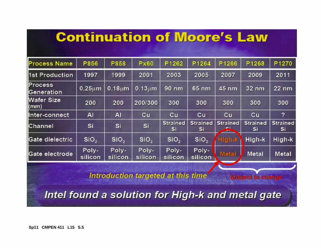
Industry Example: IBM Cu11 (0.13 um)
Dual-VDD (Voltage Island)
ASIC Cu11 (130nm) Library : Dual-vt libraryNominal Vt level (~300mv)Low Vt level (~210mv)
Low-vt version has same physical footprint~15% improvement in gate delay10 i i l k
Sp11 CMPEN 411 L15 S.3
~10x increase in leakage power

How about Gate Leakage?lti l t id (S l t t l DATE 2004)multiple gate oxide (Sylvester et.al., DATE-2004)
Sp11 CMPEN 411 L15 S.4
Sp11 CMPEN 411 L15 S.5

Dynamic CMOS(In _________ circuits at every point in time (except when
switching) the output is connected to either GND or VDDvia a low resistance path.
fan-in of N requires ______ devices
_________ circuits rely on the temporary storage of signal values on the capacitance of high impedance nodesnodes.
requires only _________ transistorstakes a sequence of ___________ and conditional
h t li l i f ti__________phases to realize logic functions
Sp11 CMPEN 411 L15 S.6
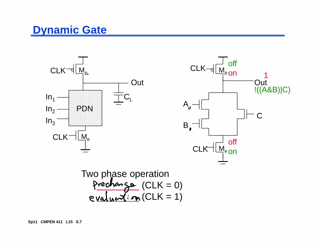
Dynamic Gate
MpCLK CLK Mp on 1off
In1
I PDN
Out
CL
Out
A
on 1
!((A&B)|C)
In2 PDNIn3
MCLK
A
BC
MeCLKCLK Me
offon
Two phase operation________ (CLK = 0)
(CLK = 1)
Sp11 CMPEN 411 L15 S.7
________ (CLK = 1)

Conditions on OutputO fOnce the output of a dynamic gate is discharged, it cannot be charged again until the next precharge operation.
Inputs to the gate can make ________ transition(s) during evaluation.
Output state is stored on CLp L
Sp11 CMPEN 411 L15 S.8

Properties of Dynamic GatesLogic function is implemented by the PDN onlyLogic function is implemented by the PDN only
number of transistors is _____(versus 2N for static complementary CMOS)should be smaller in area than static complementary CMOSshould be smaller in area than static complementary CMOS
Full swing outputs (VOL = GND and VOH = VDD)
Non-ratioed - sizing of the devices is not important for proper functioning (only for performance)
F t it hi dFaster switching speedsreduced load capacitance due to lower number of transistors per gate (Cint) so a reduced logical effortreduced load capacitance due to smaller fan-out (Cext)no Isc, so all the current provided by PDN goes into discharging CL
Ignoring the influence of precharge time on the switching speed of
Sp11 CMPEN 411 L15 S.9
Ignoring the influence of precharge time on the switching speed of the gate, tpLH = 0 but the presence of the evaluation transistor slows down the tpHL
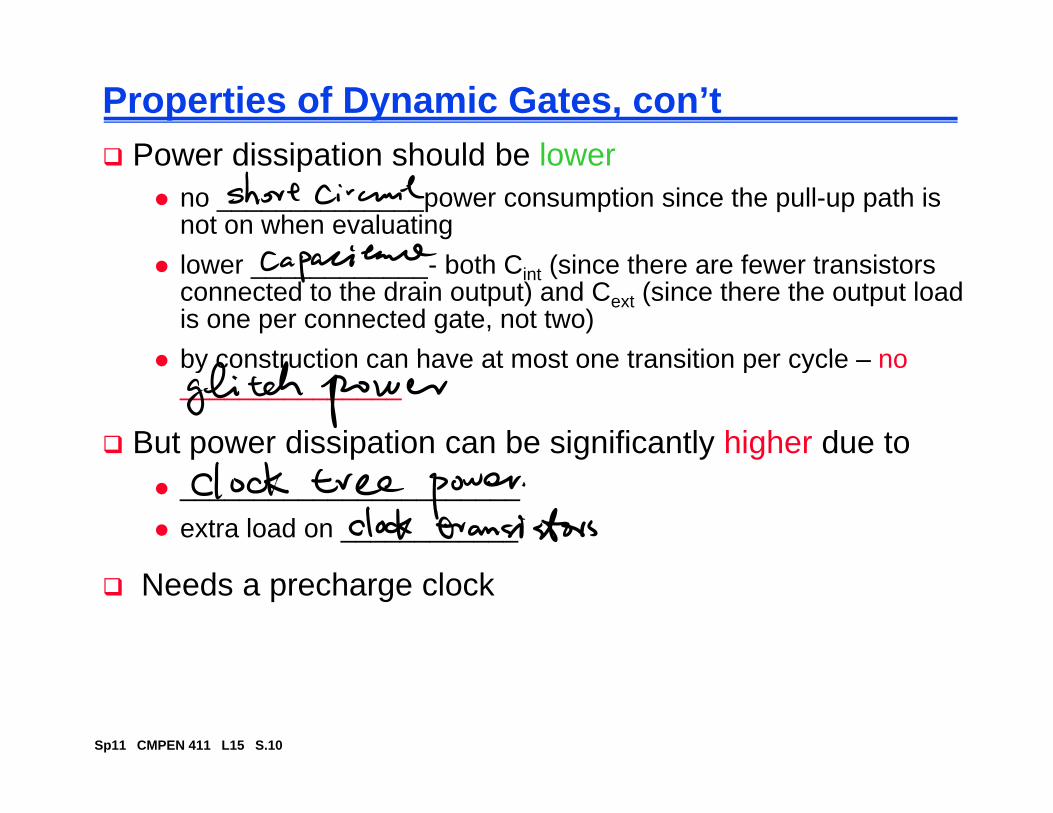
Properties of Dynamic Gates, con’tPower dissipation should be lowerPower dissipation should be lower
no ______________power consumption since the pull-up path is not on when evaluatinglower ____________- both Cint (since there are fewer transistors connected to the drain output) and Cext (since there the output load is one per connected gate, not two)by construction can have at most one transition per cycle noby construction can have at most one transition per cycle – no _______________
But power dissipation can be significantly higher due top p g y g_______________________extra load on ____________
Needs a precharge clock
Sp11 CMPEN 411 L15 S.10
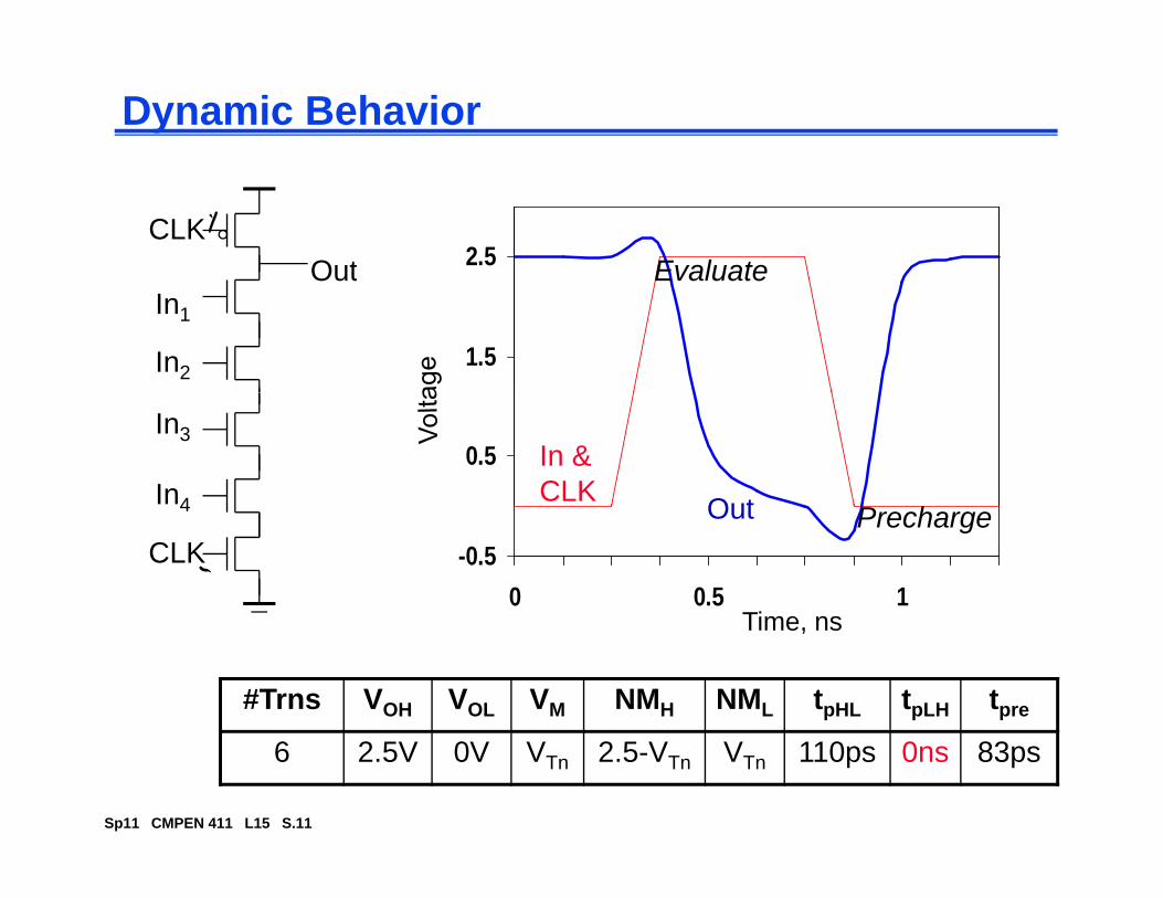
Dynamic Behavior
2.5CLK
Out Evaluate
1.5
In1
In2
Out Evaluate
0.5In3
In4
In &CLK Out
-0.50 0.5 1
CLK
4 Out
Time ns
Precharge
Time, ns
#Trns VOH VOL VM NMH NML tpHL tpLH tpre
Sp11 CMPEN 411 L15 S.11
6 2.5V 0V VTn 2.5-VTn VTn 110ps 0ns 83ps

Gate Parameters are Time IndependentThe amount by which the output voltage drops is aThe amount by which the output voltage drops is a strong function of the input voltage and the available evaluation time.
Noise needed to corrupt the signal has to be larger if the evaluation time is short – i.e., the switching threshold is truly time independent.
2.5
V)
CLK
Vout (VG=0.45)
0 5
1.5
Volta
ge (V
Vout (VG=0.55)Vout (VG=0.5)
Vout (VG 0.45)
-0.5
0.5V
VG
Sp11 CMPEN 411 L15 S.12
0 20 40 60 80 100Time (ns)

Power Consumption of Dynamic Gate
In
MpCLKOut
CIn1
In2 PDNIn3
CL
MeCLK
Power only dissipated when previous Out = 0
Sp11 CMPEN 411 L15 S.13
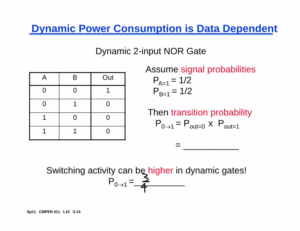
Dynamic Power Consumption is Data Dependent
Dynamic 2-input NOR Gate
Assume signal probabilitiesA B Out
0 0 1
Assume signal probabilitiesPA=1 = 1/2PB=1 = 1/2
0 1 0
1 0 0
1 1 0
Then transition probabilityP0→1 = Pout=0 x Pout=1
1 1 0
= ___________
Switching activity can be higher in dynamic gates!P0→1 =__________
Sp11 CMPEN 411 L15 S.14
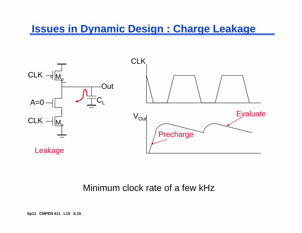
Issues in Dynamic Design : Charge Leakage
CLK
CLK
CL
CLKOut
A=0
Mp
CL
CLK
A=0
Me
VOutEvaluate
Leakage
Precharge
Minimum clock rate of a few kHz
Sp11 CMPEN 411 L15 S.15
Minimum clock rate of a few kHz

Issues in Dynamic Design : Charge Leakage
CLK
CLK3
4
CL
CLKOut
A=0
Mp
1
3
CL
CLK
A=0
Me
VOutEvaluate
2
Leakage sources
Precharge
Minimum clock rate of a few kHz
Sp11 CMPEN 411 L15 S.16
Minimum clock rate of a few kHz

Impact of Charge LeakageOutput settles to an intermediate voltage determined byOutput settles to an intermediate voltage determined by a resistive divider of the pull-up and pull-down networks
Once the output drops below the switching threshold of the f t l i t th t t i i t t d l ltfan-out logic gate, the output is interpreted as a low voltage.
2 5CLK
1.5
2.5
ge (V
)
Out
0.5Volta
g Out
-0.50 20 40
Sp11 CMPEN 411 L15 S.17
0 20 40
Time (ms)
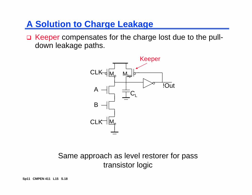
A Solution to Charge LeakageKeeper compensates for the charge lost due to the pull
Keeper
Keeper compensates for the charge lost due to the pull-down leakage paths.
CLK Mp
!Out
Mkp
Keeper
CLA
B
!Out
CLK Me
Same approach as level restorer for pass
Sp11 CMPEN 411 L15 S.18
pp ptransistor logic
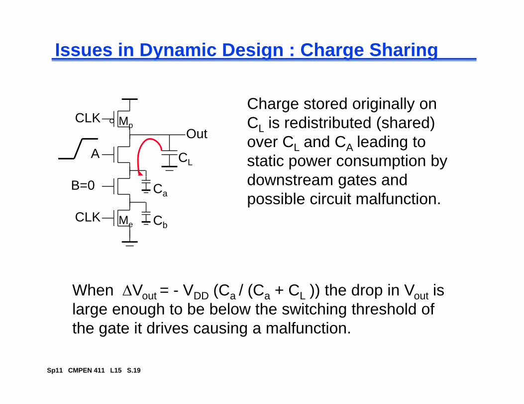
Issues in Dynamic Design : Charge Sharing
CLK Mp
Charge stored originally on CL is redistributed (shared)
CLA
Outp CL is redistributed (shared)
over CL and CA leading to static power consumption by d t t d
CLK
Ca
Cb
B=0
Me
downstream gates and possible circuit malfunction.
b
When ΔVout = - VDD (Ca / (Ca + CL )) the drop in Vout is large enough to be below the switching threshold of the gate it drives causing a malfunction
Sp11 CMPEN 411 L15 S.19
the gate it drives causing a malfunction.
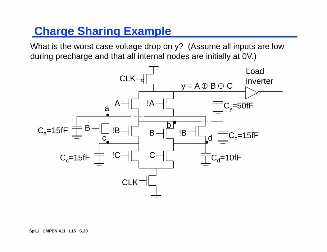
Charge Sharing ExampleWhat is the worst case voltage drop on y? (Assume all inputs are low
CLK
What is the worst case voltage drop on y? (Assume all inputs are low during precharge and that all internal nodes are initially at 0V.)
Loadi t
Cy=50fF
CLK
A !A
y = A ⊕ B ⊕ C inverter
a y
B !B B !BCa=15fF Cb=15fF
a
bdc
C!CCc=15fF Cd=10fF
CLK
Sp11 CMPEN 411 L15 S.20
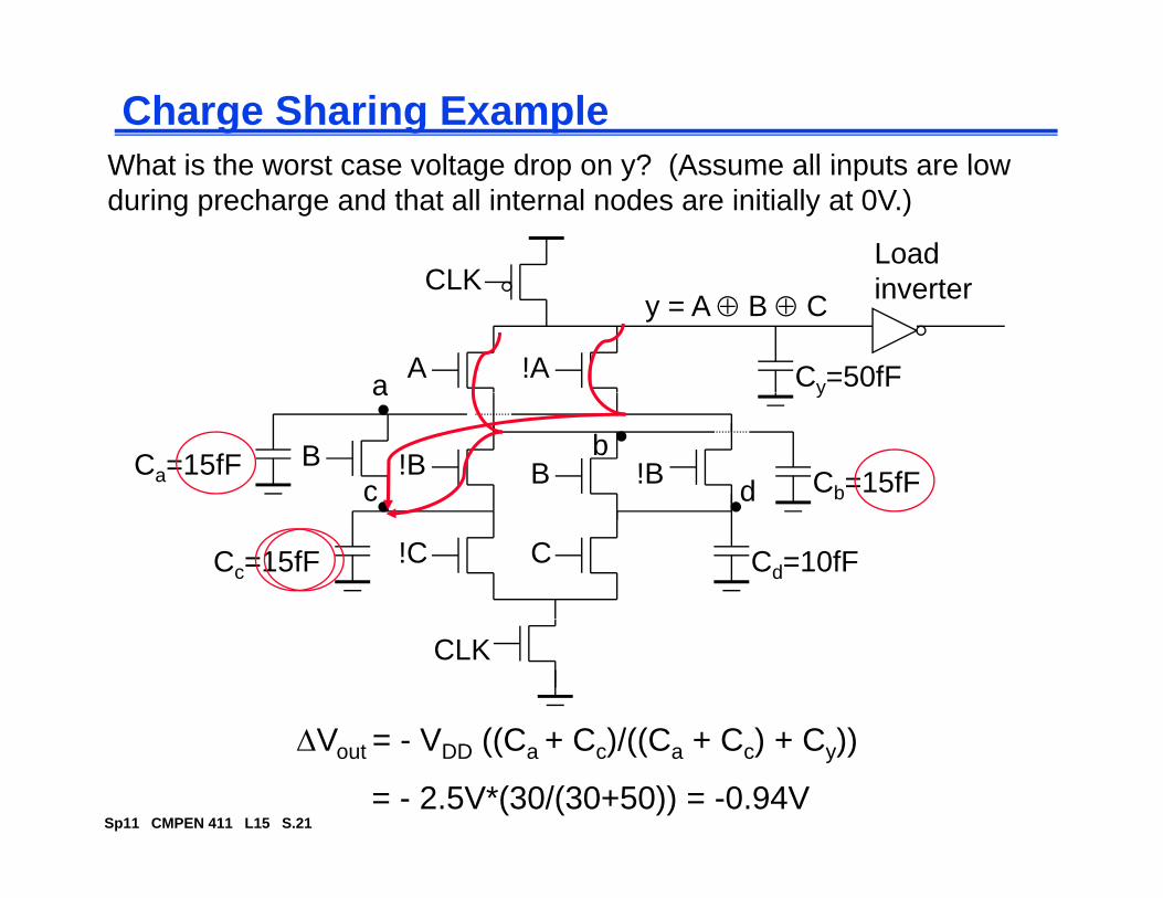
Charge Sharing ExampleWhat is the worst case voltage drop on y? (Assume all inputs are lowWhat is the worst case voltage drop on y? (Assume all inputs are low during precharge and that all internal nodes are initially at 0V.)
CLKLoadi t
Cy=50fF
CLK
A !A
y = A ⊕ B ⊕ C inverter
a y
B !B B !BCa=15fF Cb=15fF
a
bdc
C!CCc=15fF Cd=10fF
CLK
ΔV V ((C + C )/((C + C ) + C ))
Sp11 CMPEN 411 L15 S.21
ΔVout = - VDD ((Ca + Cc)/((Ca + Cc) + Cy))
= - 2.5V*(30/(30+50)) = -0.94V

Solution to Charge Redistribution
CLK M M CLKCLK Mp
AOut
MkpCLK
CLK Me
B
CLK Me
Precharge internal nodes using a clock-driven transistor (at the cost of increased area and power)
Sp11 CMPEN 411 L15 S.22
area and power)
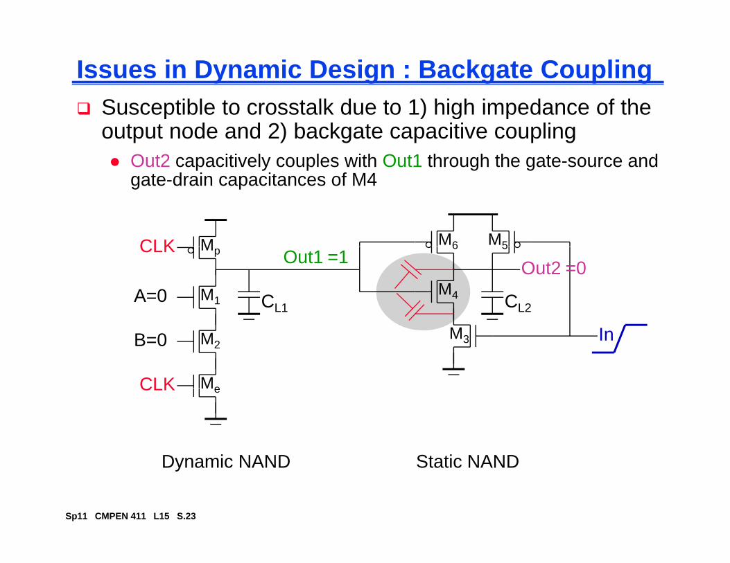
Issues in Dynamic Design : Backgate CouplingSusceptible to crosstalk due to 1) high impedance of theSusceptible to crosstalk due to 1) high impedance of the output node and 2) backgate capacitive coupling
Out2 capacitively couples with Out1 through the gate-source and t d i it f M4
CLK M
gate-drain capacitances of M4
M5M6
CL1
CLK
A=0
Out1Mp
Out2
CL2
=1 =0M1
M4
56
CLK
B=0
Me
InM2M3
CLK Me
Dynamic NAND Static NAND
Sp11 CMPEN 411 L15 S.23
Dynamic NAND Static NAND
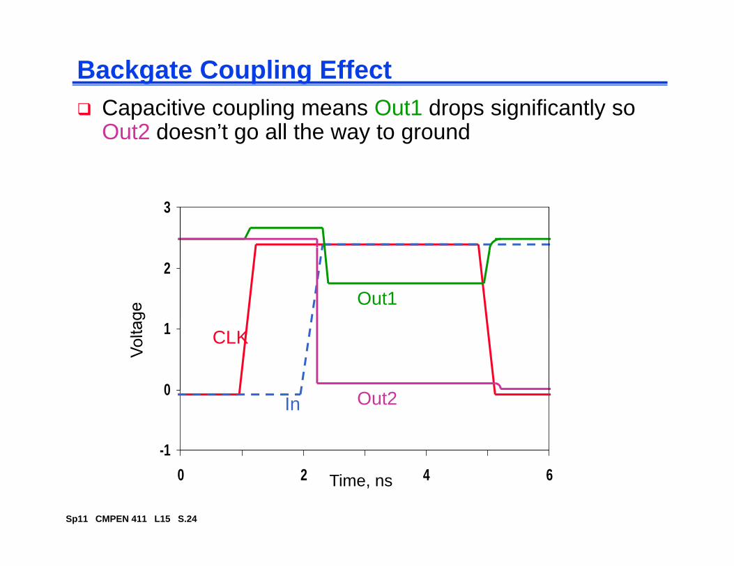
Backgate Coupling EffectCapacitive coupling means Out1 drops significantly soCapacitive coupling means Out1 drops significantly so Out2 doesn’t go all the way to ground
3
2
Out1
0
1 CLK
-1
0In Out2
Sp11 CMPEN 411 L15 S.24
0 2 4 6Time, ns
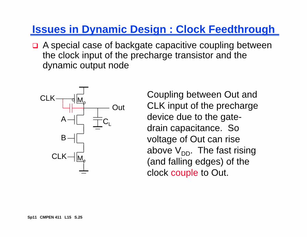
Issues in Dynamic Design : Clock FeedthroughA special case of backgate capacitive coupling betweenA special case of backgate capacitive coupling between the clock input of the precharge transistor and the dynamic output node
CLK MpCoupling between Out and CLK i t f th h
CLA
Outp CLK input of the precharge
device due to the gate-drain capacitance. So
CLK
B
Me
voltage of Out can rise above VDD. The fast rising (and falling edges) of the(and falling edges) of the clock couple to Out.
Sp11 CMPEN 411 L15 S.25

Clock Feedthrough
CLK Clock feedthrough
2.5In1
I
OutClock feedthrough
1.5In2
In3In &
0.5
CLK
In4
In &CLK
Out
-0.50 0.5 1Time, ns
Clock feedthrough
Sp11 CMPEN 411 L15 S.26
Clock feedthrough

Issues in Dynamic Design : Cascading Gates
CLK
V
CLKCLK
Out1I
Mp MpCLK
Out2 In
CLK
In
Me MeCLK
Out1 VTn
t
Out2 ΔV
t
Only a single 0 → 1 transition allowed at the
Sp11 CMPEN 411 L15 S.27
inputs during the evaluation period!

Domino Logic
MpCLK Out1MpCLK
Out2Mkp
1 → 11 → 0
In1
In2 PDN In4 PDNIn
1 → 00 → 00 → 1
In3
MeCLK
In5
MeCLK
Sp11 CMPEN 411 L15 S.28
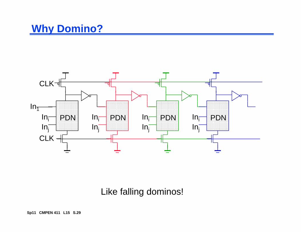
Why Domino?
CLK
In1
Ini PDNInj
IniInj
PDN Ini PDNInj
Ini PDNInj
CLKj j j j
Lik f lli d i !
Sp11 CMPEN 411 L15 S.29
Like falling dominos!
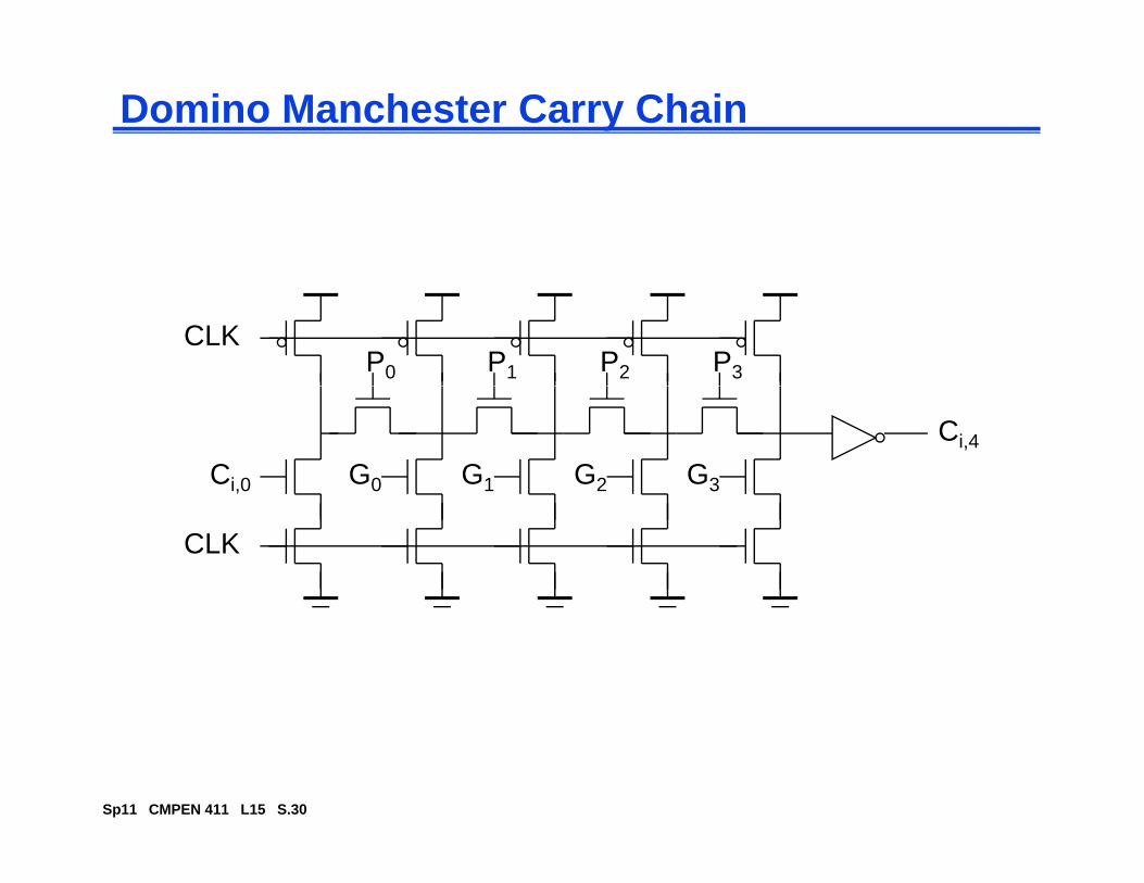
Domino Manchester Carry Chain
CLKP0 P1 P2 P3
Ci,0 G0 G1 G2 G3
Ci,4
CLK
Sp11 CMPEN 411 L15 S.30

Domino Zero Detector
I I I I I I IIIn7 In6 In5 In4 In3 In2 In0In1
not zero
CLK
How would you build it in static CMOS?
Sp11 CMPEN 411 L15 S.31

Domino Comparator
CLKA3 A2 A1 A0
Out
B3 B2 B1 B0
Sp11 CMPEN 411 L15 S.32

Properties of Domino Logic
Only non-inverting logic can be implemented, fixes include
can reorganize the logic using Boolean transformationsuse differential logic (dual rail)use np-CMOS (zipper)p ( pp )
Very high speedVery high speedtpHL = 0static inverter can be optimized to match fan-out (separation of fan-in and fan-out capacitances)
Sp11 CMPEN 411 L15 S.33
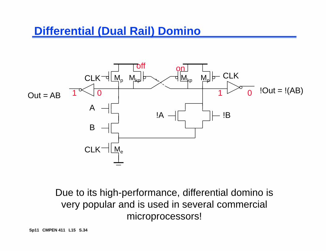
Differential (Dual Rail) Domino
MCLK M CLKM Monoff
A
MpCLK!Out = !(AB)
MkpCLK
Out = AB
Mkp Mp
1 0 1 0
A
B!A !B
MeCLK
Due to its high-performance, differential domino is very popular and is used in several commercial
Sp11 CMPEN 411 L15 S.34
very popular and is used in several commercial microprocessors!

Other Domino VariationsfMultiple output domino logic – exploits the fact that
certain outputs are subsets of other outputs to generate a number of logic functions in a single gate.
Compound domino
MCLK MCLK M
A
MpCLK
D
MpCLK Mp
A
B
D
E G
MeCLK
C
MeCLK
F
Me
H
Sp11 CMPEN 411 L15 S.35
e e e

np-CMOS (Zipper)
MpCLK Out1Me!CLK
1 → 11 0
In1
In2 PDN
In4 PUNIn5
1 → 0
0 0In3
MeCLK Mp!CLK
Out2(to PDN)
0 → 00 → 1
to otherPDN’s
to otherPUN’s
Only 0 → 1 transitions allowed at inputs of PDN O l 1 0 t iti ll d t i t f PUN
Sp11 CMPEN 411 L15 S.36
Only 1 → 0 transitions allowed at inputs of PUN

np-CMOS Adder Circuit
Sum1!A !B!B !C
!CLK CLK 1 → x0 → x
C2
!A1
!A1
!B1!B1!A1!A1!B1
!B1
!C1
!C1
!CLK 0 → x
1 → x
!CLK
2!CLKCLK
C0
!C1
A0
B0B0 A0
A0
CLK!CLK
1 → x0 → x
B0 C0
C0
!Sum0B0A0
0
CLK !CLK 0 → x1 → x
Sp11 CMPEN 411 L15 S.37

DCVS Logic
InOut !Out
1 0on off
In1
In2PDN1!In1
!In2
PDN2off on!In2
PDN1 and PDN2 are mutually exclusive
Sp11 CMPEN 411 L15 S.38

DCVS Logic (Differential Cascade Voltage Switch
IOut !Out
1 0→ 0 on off→ on→ off → 1
In1
In2PDN1!In1
!In
PDN2off→ on on→ off!In2
on→ off
PDN1 and PDN2 are mutually exclusive
Sp11 CMPEN 411 L15 S.39
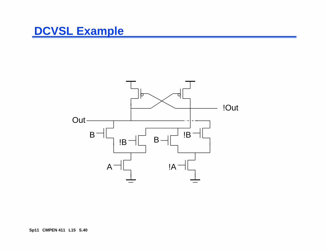
DCVSL Example
!OutOut
!Out
B B!B!B
A !A
B!B
Sp11 CMPEN 411 L15 S.40
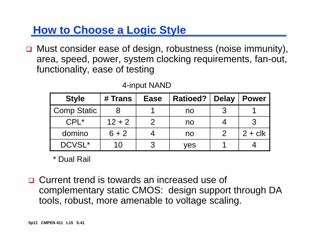
How to Choose a Logic Stylef ( )Must consider ease of design, robustness (noise immunity),
area, speed, power, system clocking requirements, fan-out, functionality, ease of testing
Style # Trans Ease Ratioed? Delay Power4-input NAND
Comp Static 8 1 no 3 1CPL* 12 + 2 2 no 4 3
domino 6 + 2 4 no 2 2 + clkDCVSL* 10 3 yes 1 4
* Dual Rail
Current trend is towards an increased use of complementary static CMOS: design support through DA t l b t bl t lt li
Sp11 CMPEN 411 L15 S.41
tools, robust, more amenable to voltage scaling.
Itanium 2 Domino Circuitry
Integer execution unit
Multimedia execution unit
2 Floating point units
Register Files
Out of order control issue logic g
Source: “Advanced Domino Circuit Design” Intel– Source: Advanced Domino Circuit Design , Intel, Tom Grutkowski, DATE 2004
Sp11 CMPEN 411 L15 S.42

What is Soft Error
Soft errors are circuit errors caused due to excess charge carriers induced primarily by external radiations
These errors cause an upset event but the circuit it self is not damaged.
Same a SEU (single event upset)
Sp11 CMPEN 411 L15 S.43

Soft Errors
G
The Phenomena
A particle strikeCurrent
n+n++ - + -+ -
++- + -+
p substraten channel
+ -+ -
+ - + -
B
Sp11 CMPEN 411 L15 S.44
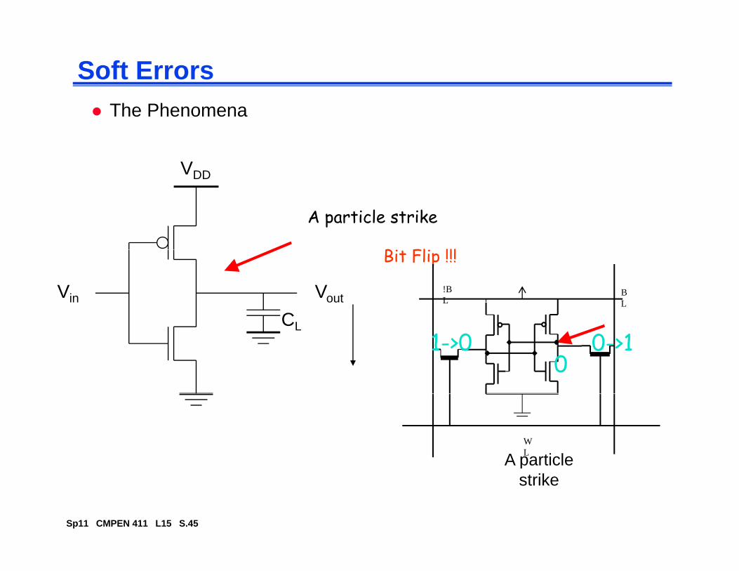
Soft ErrorsTh PhThe Phenomena
VDDDD
A particle strike
Bi Fli !!!
Vout
CL
Vin
Bit Flip !!!
!BL
BL
CL0->11->0
0
A particle WL
Sp11 CMPEN 411 L15 S.45
pstrike
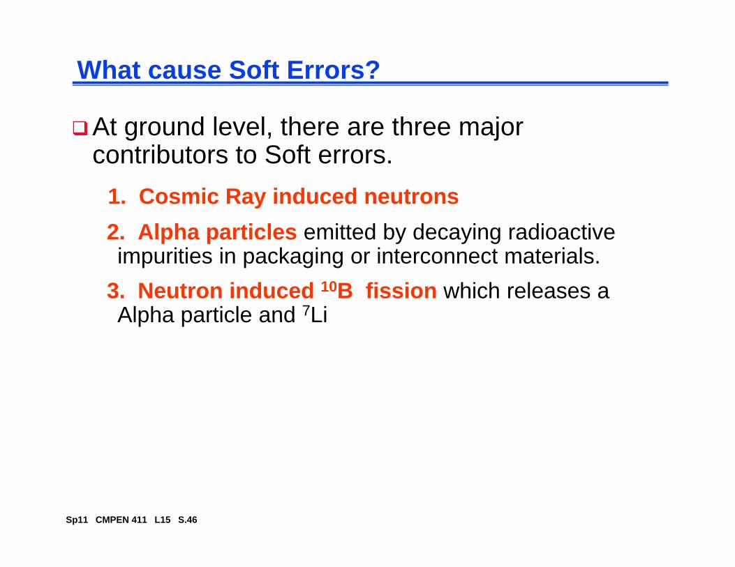
What cause Soft Errors?
At ground level, there are three major contributors to Soft errors.
1. Cosmic Ray induced neutrons2. Alpha particles emitted by decaying radioactive i iti i k i i t t t i limpurities in packaging or interconnect materials.
3. Neutron induced 10B fission which releases a Alpha particle and 7LiAlpha particle and Li
Sp11 CMPEN 411 L15 S.46

Evidence of Cosmic Ray Strikes
Documented strikes in large servers found in error logsNormand, “Single Event Upset at Ground Level,” IEEE Transactions
N l S i V l 43 N 6 D b 1996on Nuclear Science, Vol. 43, No. 6, December 1996.
Sun Microsystems, 2000Cosmic ray strikes on L2 cache with no error detection or correctionCosmic ray strikes on L2 cache with no error detection or correction- caused Sun’s flagship servers to suddenly and mysteriously
crash!Companies affectedCompanies affected- Baby Bell (Atlanta), America Online, Ebay, & dozens of other
corporations Verisign moved to IBM Unix servers (for the most part)- Verisign moved to IBM Unix servers (for the most part)
Sp11 CMPEN 411 L15 S.47
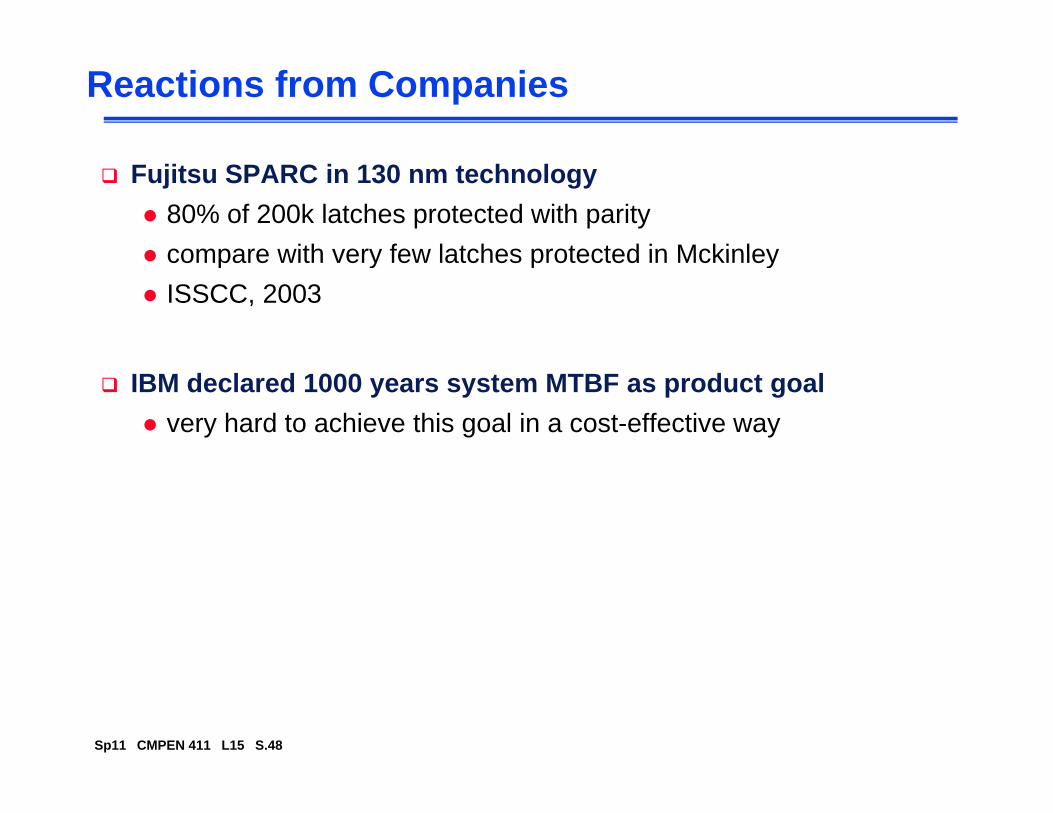
Reactions from Companies
Fujitsu SPARC in 130 nm technology80% of 200k latches protected with paritycompare with very few latches protected in Mckinleycompare with very few latches protected in MckinleyISSCC, 2003
IBM declared 1000 years system MTBF as product goalvery hard to achieve this goal in a cost-effective way
Sp11 CMPEN 411 L15 S.48

Sp11 CMPEN 411 L15 S.49

Space redundancy: Redundant Logic
Logic 1Logic 1
Logic 2 Voter
Logic3Point of failure!!
Logic3
Sp11 CMPEN 411 L15 S.50
Next Lecture and RemindersNext lectureNext lecture
Timing metrics, static sequential circuits- Reading assignment – Rabaey, et al, 7.1-7.2
Sp11 CMPEN 411 L15 S.51
Top Related