


Languages
Pages
Legal


CMPEN 411 L01 S1
CMPEN 411VLSI Digital Circuits
Lecture 01: Introduction
Kyusun Choi
CMPEN 411 Course Website link at: http://www.cse.psu.edu/~kyusun/teach/teach.html
[Adapted from Rabaey‟s Digital Integrated Circuits, Second Edition, ©2003 J. Rabaey, A. Chandrakasan, B. Nikolic]

CMPEN 411 L01 S2
How Do the Pieces Fit Together?
I/O systemInstr. Set Proc.
Compiler
OperatingSystem
Application
Digital Design
Circuit Design
Instruction SetArchitecture
Firmware
Coordination of many levels of abstraction
Under a rapidly changing set of forces
Design, measurement, and evaluation
Datapath & Control
Memory
system
CMPEN 411 L01 S3
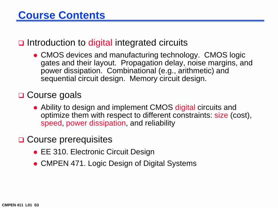
Course Contents
Introduction to digital integrated circuits
CMOS devices and manufacturing technology. CMOS logic gates and their layout. Propagation delay, noise margins, and power dissipation. Combinational (e.g., arithmetic) and sequential circuit design. Memory circuit design.
Course goals
Ability to design and implement CMOS digital circuits and optimize them with respect to different constraints: size (cost), speed, power dissipation, and reliability
Course prerequisites
EE 310. Electronic Circuit Design
CMPEN 471. Logic Design of Digital Systems

CMPEN 411 L01 S4
Background from CMPEN 471 and EE 310
Basic circuit theory
resistance, capacitance, inductance
MOS gate characteristics
Hardware description language
VHDL or verilog
Use of modern EDA tools
simulation, synthesis, validation (e.g., Synopsys)
schematic capture tools (e.g., LogicWorks)
Logic design
logical minimization, FSMs, component design
CMPEN 411 L01 S5
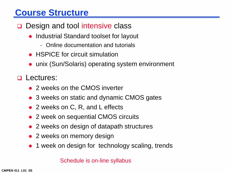
Course Structure
Design and tool intensive class
Industrial Standard toolset for layout
- Online documentation and tutorials
HSPICE for circuit simulation
unix (Sun/Solaris) operating system environment
Lectures:
2 weeks on the CMOS inverter
3 weeks on static and dynamic CMOS gates
2 weeks on C, R, and L effects
2 week on sequential CMOS circuits
2 weeks on design of datapath structures
2 weeks on memory design
1 week on design for technology scaling, trends
Schedule is on-line syllabus

CMPEN 411 L01 S6
What is the most important invention for the last 50 years?

CMPEN 411 L01 S7
The evolution of IC
When was the first transistor invented?
A. 1945 B. 1947 C. 1951 D. 1958
The inventors were in which company?
A. IBM B. Bell Lab C. TI D. Motorola
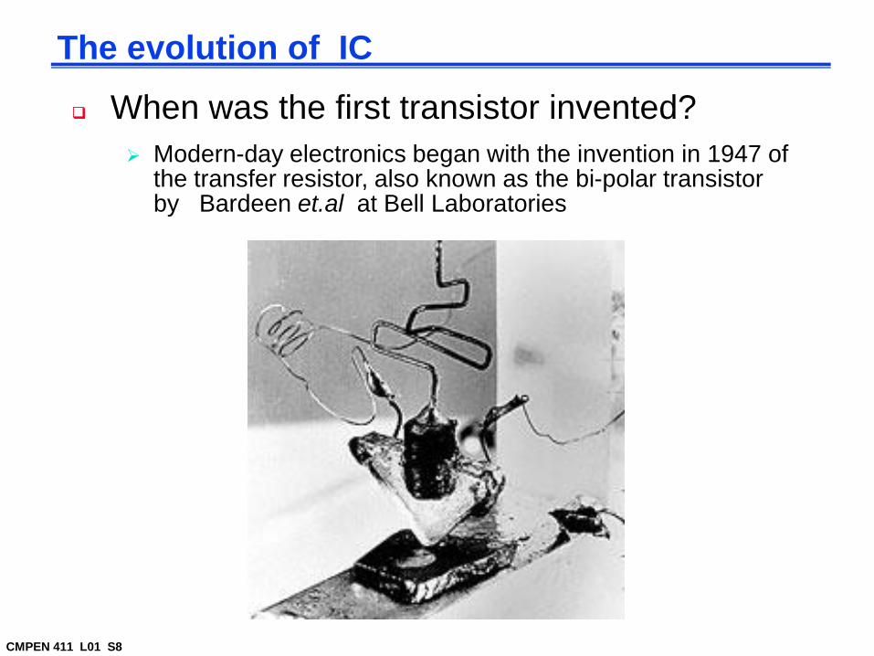
CMPEN 411 L01 S8
The evolution of IC
When was the first transistor invented?
Modern-day electronics began with the invention in 1947 of the transfer resistor, also known as the bi-polar transistor by Bardeen et.al at Bell Laboratories

CMPEN 411 L01 S9
The evolution of IC
When was the first IC invented?
A. 1956 B. 1958 C. 1959 D. 1961
The inventor was with which company?
A. IBM B. Bell Labs C. TI D. Motorola

CMPEN 411 L01 S10
The evolution of IC
When was the first IC (integrated circuit) invented?
In 1958 the integrated circuit was born when Jack Kilby at Texas Instruments successfully interconnected, by hand, several
transistors, resistors and capacitors on a single substrate

CMPEN 411 L01 S11
Transistor Revolution
Transistor –Bardeen et.al. (Bell Labs) in 1947
Bipolar transistor – Schockley in 1949
First bipolar digital logic gate – Harris in 1956
First monolithic IC – Jack Kilby in 1958
First commercial IC logic gates – Fairchild 1960

CMPEN 411 L01 S12
MOSFET Technology
MOSFET transistor - Lilienfeld (Canada) in 1925 and Heil (England) in 1935
CMOS – 1960‟s, but plagued with manufacturing problems (used in watches due to their power limitations)
PMOS in 1960‟s (calculators)
NMOS in 1970‟s (4004, 8080) – for speed
CMOS in 1980‟s – preferred MOSFET technology because of power benefits
BiCMOS, Gallium-Arsenide, Silicon-Germanium
SOI, Copper-Low K, strained silicon, High-k gate oxide...
CMPEN 411 L01 S13
CMPEN 411 VLSI Digital Circuits
Kyusun Choi
VLSI Chip Pictures

CMPEN 411 L01 S14

CMPEN 411 L01 S15

CMPEN 411 L01 S16

CMPEN 411 L01 S17
Fig. 12 Increase in wafer sizes, showing the increased number of dice (chips) per wafer available when increasing the wafer area. (a) 100-mm (4-in.) wafer. (b) 150-mm (6-in.) wafer. (c) 300-mm (12-in.) wafer. (Intel Corp.)
Fig. 7 Person with lint-free garments in a vertical laminar-flow clean room forintegrated-circuit fabrication with 300-mm (12-in.) wafer. (Personnel do not handle wafers in this manner. This was done just for the photograph.) (Intel Corp.)
CMPEN 411 L01 S18

CMPEN 411 L01 S19

CMPEN 411 L01 S20

CMPEN 411 L01 S21

CMPEN 411 L01 S22

CMPEN 411 L01 S23

CMPEN 411 L01 S24

CMPEN 411 L01 S25

CMPEN 411 L01 S26
CMPEN 411 L01 S27

CMPEN 411 L01 S28

CMPEN 411 L01 S29
Fig. 1. Cross-section of a 64-bit
high-speed processor in a 90nm
technology. (Courtesy: IBM)

CMPEN 411 L01 S30

CMPEN 411 L01 S31

CMPEN 411 L01 S32

CMPEN 411 L01 S33

CMPEN 411 L01 S34

CMPEN 411 L01 S35

CMPEN 411 L01 S36
Programmable Logic Gate Array

CMPEN 411 L01 S37
Programmable Logic Gate Array
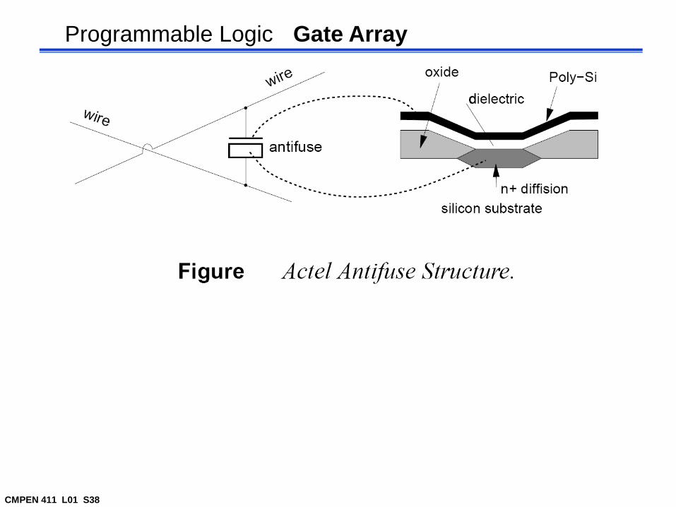
CMPEN 411 L01 S38
Programmable Logic Gate Array

CMPEN 411 L01 S39
Programmable Logic Gate Array
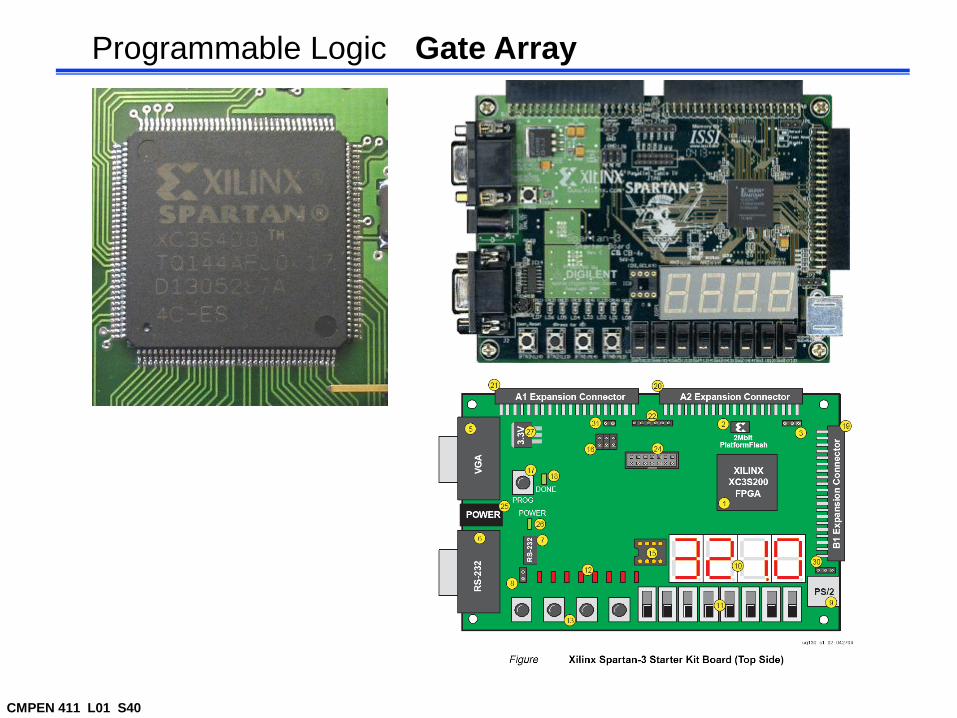
CMPEN 411 L01 S40
Programmable Logic Gate Array
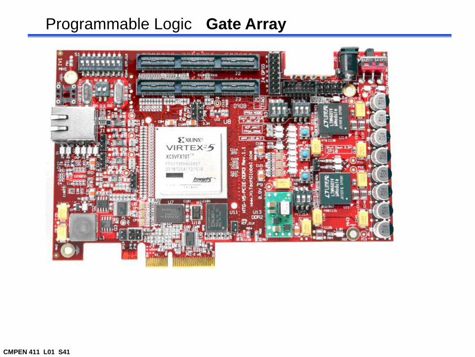
CMPEN 411 L01 S41
Programmable Logic Gate Array

CMPEN 411 L01 S42
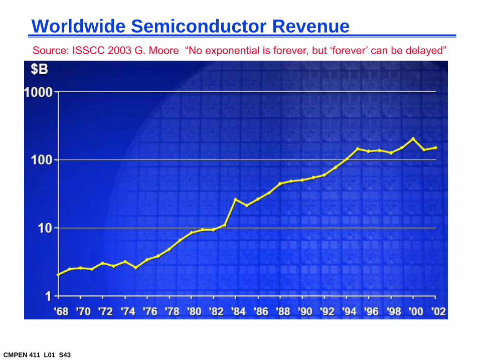
CMPEN 411 L01 S43
Worldwide Semiconductor RevenueSource: ISSCC 2003 G. Moore “No exponential is forever, but „forever‟ can be delayed”

CMPEN 411 L01 S44
Transistors shipped per year
How many transistors you can buy with 1$?

CMPEN 411 L01 S45
Average Transistor Price by Year

CMPEN 411 L01 S46
1’’ Wafer in 1964 vs. 300 mm (12 ”) Wafer in 2003

CMPEN 411 L01 S47
The IC in 1961 vs. Intel Pentium 4 in 2004

CMPEN 411 L01 S48
Moore’s Law
In 1965, Gordon Moore predicted that the number of transistors that can be integrated on a die would double every 18 months (i.e., grow exponentially with time).
Amazingly visionary – million transistor/chip barrier was crossed in the 1980‟s.
2300 transistors, 108 KHz clock (Intel 4004) - 1971
16 Million transistors (Ultra Sparc III)- 1998
42 Million, 2 GHz clock (Intel P4) - 2001
125 Million, 3.4Ghz (Intel P4 Prescott)- 2004 Feb 02
234 Million, IBM Cell processor, 2005
1.7 Billion, 1.6Ghz (Intel Itanium-2)-2006, Sept.

CMPEN 411 L01 S49
Moore’s Law plot (from his original paper)

CMPEN 411 L01 S50
Moore’s Law in Microprocessors
40048008
80808085 8086
286
386
486Pentium® proc
P6
0.001
0.01
0.1
1
10
100
1000
1970 1980 1990 2000 2010
Year
Tra
nsis
tors
(M
T)
2X growth in 1.96 years!
# transistors on lead microprocessors double every 2 years
Courtesy, Intel

CMPEN 411 L01 S51
# of Transistors per Die
Source: ISSCC 2003 G. Moore “No exponential is forever, but „forever‟ can be delayed”

CMPEN 411 L01 S52
Intel 4004 Microprocessor (10000 nm) 1971
2300 transistors
13.5 mm2
108k Hz

CMPEN 411 L01 S53
Intel Pentium 4 –Prescott (2004)
90 nm
Area: 112 mm2
125 M transistors
L1-Instruction: 16K
L1-Data: 16K
L2: 1MB

CMPEN 411 L01 S54
Two chips you are seeing today
Microprocessor ASIC (Application Specific IC)
366MHz 40mm2 3.65M 40Mhz 10 mm2 500K

CMPEN 411 L01 S55
IBM Cell Overview
IBM/Toshiba/Sony joint project - 4-5 years, 400 designers, 3/9/2001, $400M, 234 million transistors, 4+ Ghz, 256 Gflops (billions of floating pointer operations per second)
P
P
U
S
P
U
S
P
U
S
P
U
S
P
U
S
P
U
S
P
U
S
P
U
S
P
U
M
I
C
R
R
A
C
B
I
C
MIB
Cell Prototype Die (Pham et al, ISSCC 2005)

CMPEN 411 L01 S56
State-of-the Art: Lead Microprocessors
Pentium 4 180 nm (2001) 1.7 G Hz 42 M transistors 217 mm2
Pentium 4 130 nm (2003) 3.2G Hz 55 M Transistors 131 mm2
Pentium 4 90 nm (2004) 3.4 Hz 125 M Transistors 112 mm2
Pentium on 65nm (2005/2006) 250 Million
Pentium on 45nm (2007) 400 to 500 Million
Freq
(HZ)
Transistors Die size
mm2
Power Date
Server IBM Power 4+ 1.7G 180M 267 N/A 2003
Itanium 2 1.5G 410M 374 130W 2003
IBM Power 5 2G 276M 389 N/A 2004/2
PC IBM Power PC970 1.8G 58M 118 42W 2003/6
Pentium 4 3.2G 55M 131 82W 2003/6
AMD Athlon 64 2.2G 105M 192 89W 2003/9
Pentium 4 (Prescott)
3.4G 125M 112 103W 2004/2
(All use 0.13 um technology except Pentium 4 – Prescott, which uses 90 nm tech)

CMPEN 411 L01 S57
State-of-the Art: Lead Microprocessors (up to date)
300mm wafer and Pentium 4 IC. Photos courtesy of Intel.

CMPEN 411 L01 S59
Die Size Growth
40048008
80808085
8086286
386486
Pentium ® procP6
1
10
100
1970 1980 1990 2000 2010
Year
Die
siz
e (
mm
)Die size grows by 14% to satisfy Moore’s Law
Courtesy, Intel

CMPEN 411 L01 S60
Clock Frequency
Lead microprocessors frequency doubles every 2 years
P6
Pentium ® proc486
3862868086
8085
8080
8008
40040.1
1
10
100
1000
10000
1970 1980 1990 2000 2010
Year
Fre
qu
en
cy (
Mh
z)
2X every 2 years
Courtesy, Intel

CMPEN 411 L01 S61
Power Dissipation
P6Pentium ® proc
486
386
2868086
80858080
80084004
0.1
1
10
100
1971 1974 1978 1985 1992 2000
Year
Po
wer
(Watt
s)
Lead Microprocessors power continues to increase
Courtesy, Intel
Power delivery and dissipation will be prohibitive

CMPEN 411 L01 S62
Power Density
4004
8008
8080
8085
8086
286386
486Pentium® proc
P6
1
10
100
1000
10000
1970 1980 1990 2000 2010
Year
Po
wer
Den
sit
y (
W/c
m2)
Hot Plate
Nuclear
Reactor
Rocket
Nozzle
Power density too high to keep junctions at low temp
Courtesy, Intel

CMPEN 411 L01 S63
Power Density
4004
8008
8080
8085
8086
286386
486Pentium® proc
P6
1
10
100
1000
10000
1970 1980 1990 2000 2010
Year
Po
wer
Den
sit
y (
W/c
m2)
Hot Plate
Nuclear
Reactor
Rocket
Nozzle
Power density too high to keep junctions at low temp
Courtesy, Intel

CMPEN 411 L01 S64
ITRS
The “International Technology Roadmap for Semiconductors” (ITRS) is the industry‟s prediction for the future of semiconductors.
It is mostly an extrapolation of existing trends.
The ITRS is often “slow”.
http://public.itrs.net

CMPEN 411 L01 S65
Technology Directions: “Old” SIA Roadmap
Year 1999 2002 2005 2008 2011 2014
Feature size (nm) 180 130 100 70 50 35
Mtrans/cm2 7 14-26 47 115 284 701
Chip size (mm2) 170 170-214 235 269 308 354
Signal pins/chip 768 1024 1024 1280 1408 1472
Clock rate (MHz) 600 800 1100 1400 1800 2200
Wiring levels 6-7 7-8 8-9 9 9-10 10
Power supply (V) 1.8 1.5 1.2 0.9 0.6 0.6
High-perf power (W) 90 130 160 170 174 183
Battery power (W) 1.4 2.0 2.4 2.0 2.2 2.4
http://public.itrs.net
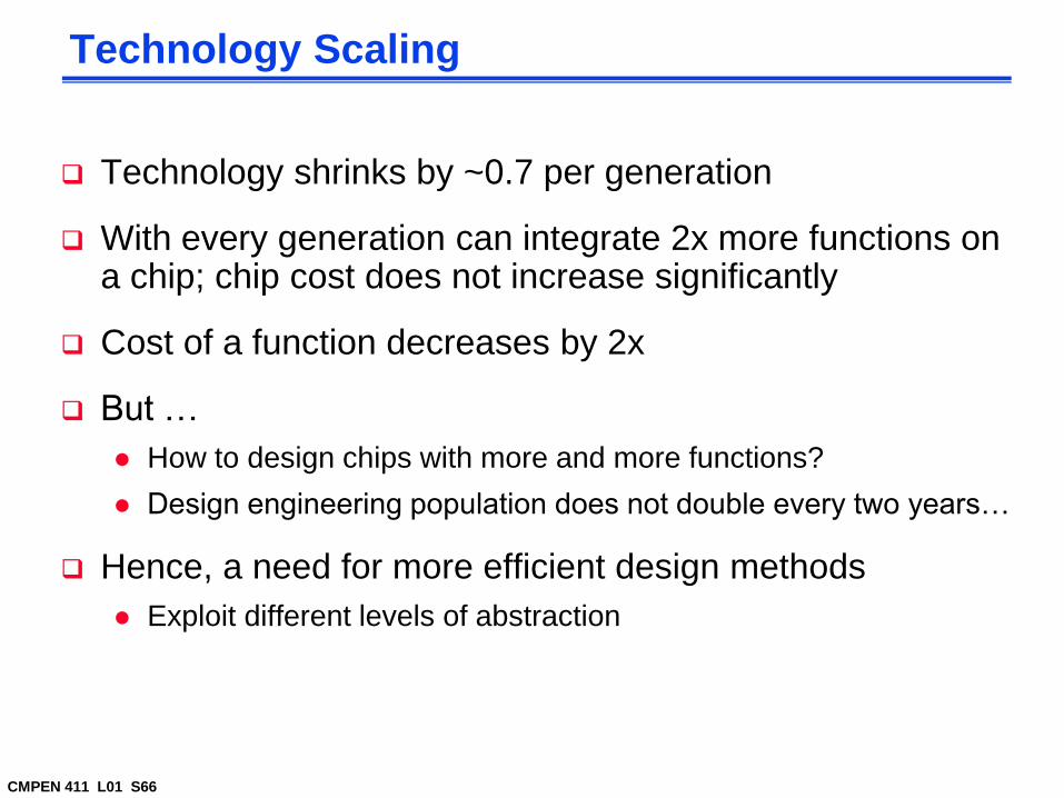
CMPEN 411 L01 S66
Technology Scaling
Technology shrinks by ~0.7 per generation
With every generation can integrate 2x more functions on a chip; chip cost does not increase significantly
Cost of a function decreases by 2x
But …
How to design chips with more and more functions?
Design engineering population does not double every two years…
Hence, a need for more efficient design methods
Exploit different levels of abstraction
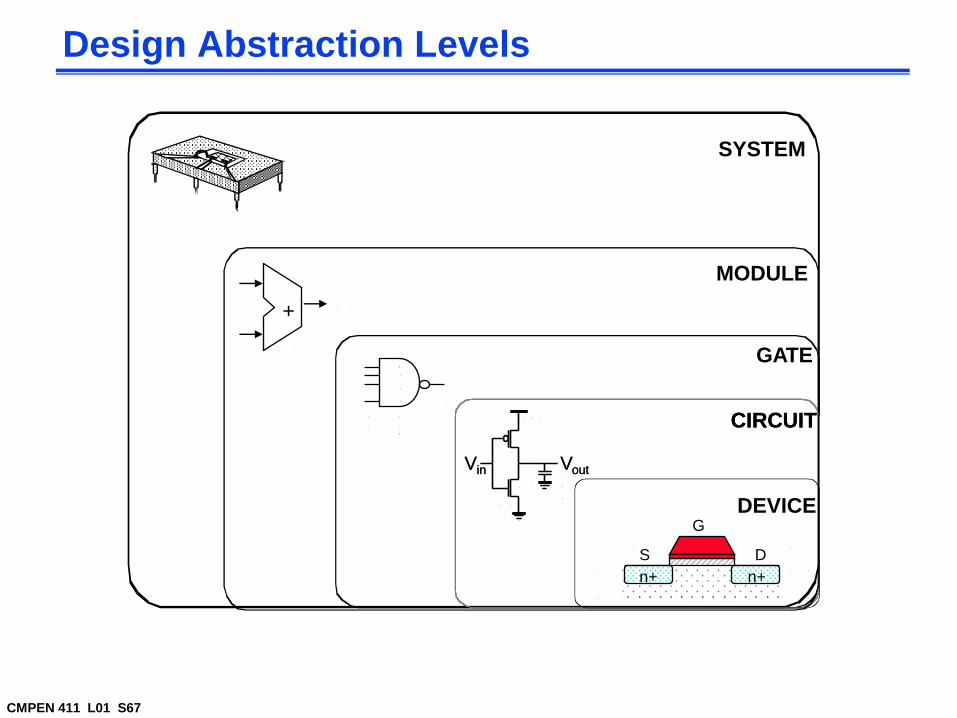
CMPEN 411 L01 S67
Design Abstraction Levels
SYSTEM
GATE
CIRCUIT
VoutVin
CIRCUIT
VoutVin
MODULE
+
DEVICE
n+
S D
n+
G
CMPEN 411 L01 S69
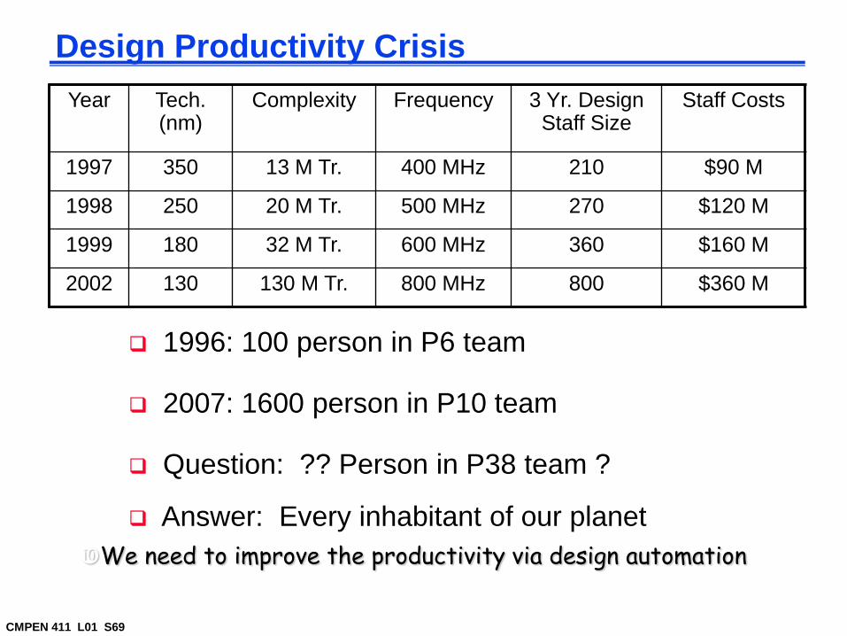
Design Productivity Crisis
We need to improve the productivity via design automation
1996: 100 person in P6 team
2007: 1600 person in P10 team
Question: ?? Person in P38 team ?
Answer: Every inhabitant of our planet
Year Tech. (nm)
Complexity Frequency 3 Yr. Design Staff Size
Staff Costs
1997 350 13 M Tr. 400 MHz 210 $90 M
1998 250 20 M Tr. 500 MHz 270 $120 M
1999 180 32 M Tr. 600 MHz 360 $160 M
2002 130 130 M Tr. 800 MHz 800 $360 M

CMPEN 411 L01 S70
Major Design Challenges
Microscopic issues
ultra-high speeds
power dissipation and supply rail drop
growing importance of interconnect
noise, crosstalk
reliability, manufacturability
clock distribution
Macroscopic issues
time-to-market
design complexity (millions of gates)
high levels of abstractions
reuse and IP, portability
systems on a chip (SoC)
tool interoperability
CMPEN 411 L01 S71
Testing and Faults
1/7/2015 71L12: Testing
CMPEN 411 L01 S72
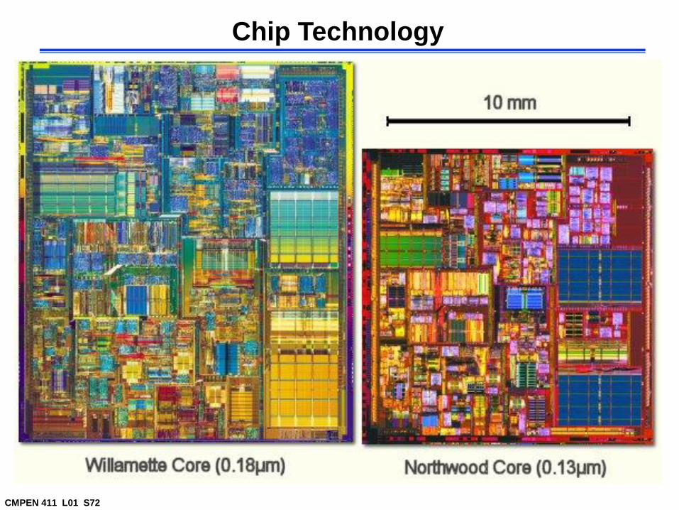
Chip Technology
1/7/2015 72L12: Testing

CMPEN 411 L01 S73
1/7/2015 73L12: Testing
Chip Technology

CMPEN 411 L01 S74
1/7/2015 74L12: Testing
Chip Technology

CMPEN 411 L01 S75
1/7/2015 75L12: Testing
Chip Technology
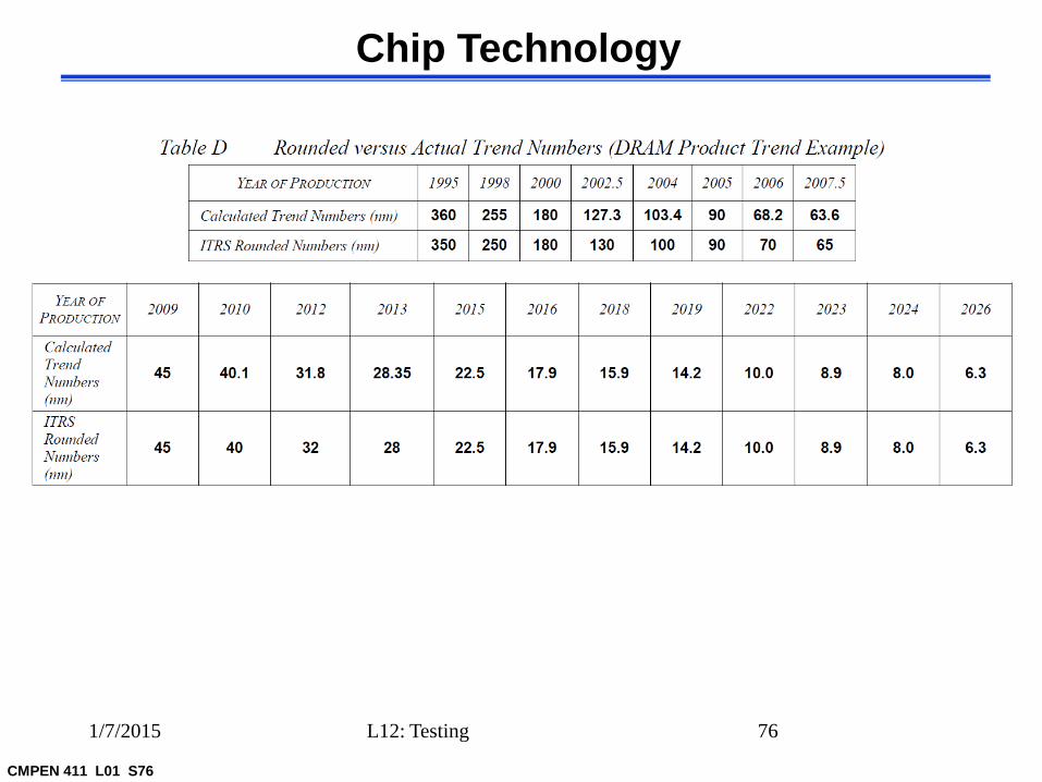
CMPEN 411 L01 S76
1/7/2015 76L12: Testing
Chip Technology

CMPEN 411 L01 S77
1/7/2015 77L12: Testing
Chip Technology

CMPEN 411 L01 S78
1/7/2015 78L12: Testing
Chip Technology
GHz frequency

CMPEN 411 L01 S79
Testing and Faults
1/7/2015 79L12: Testing

CMPEN 411 L01 S80
Testing and Faults
1/7/2015 80L12: Testing

CMPEN 411 L01 S81
Testing and Faults
1/7/2015 81L12: Testing

CMPEN 411 L01 S82
Testing and Faults
1/7/2015 82L12: Testing

CMPEN 411 L01 S83
Testing and Faults
1/7/2015 83L12: Testing

CMPEN 411 L01 S84
Testing and Faults
1/7/2015 84L12: Testing

CMPEN 411 L01 S85
Testing and Faults
1/7/2015 85L12: Testing
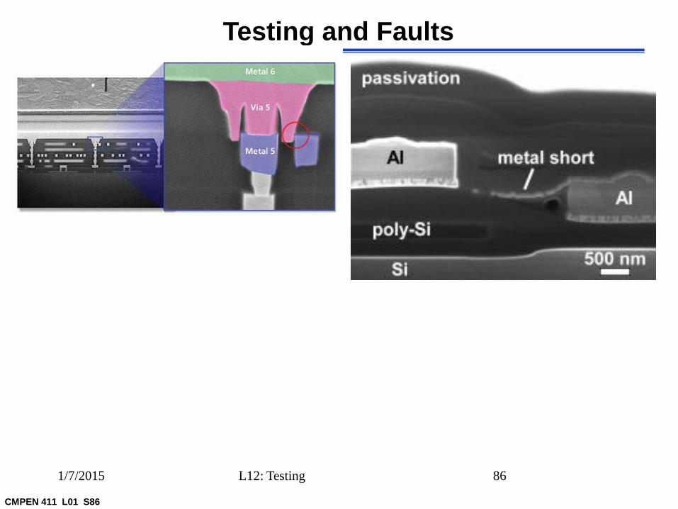
CMPEN 411 L01 S86
Testing and Faults
1/7/2015 86L12: Testing

CMPEN 411 L01 S87
Testing and Faults
1/7/2015 87L12: Testing
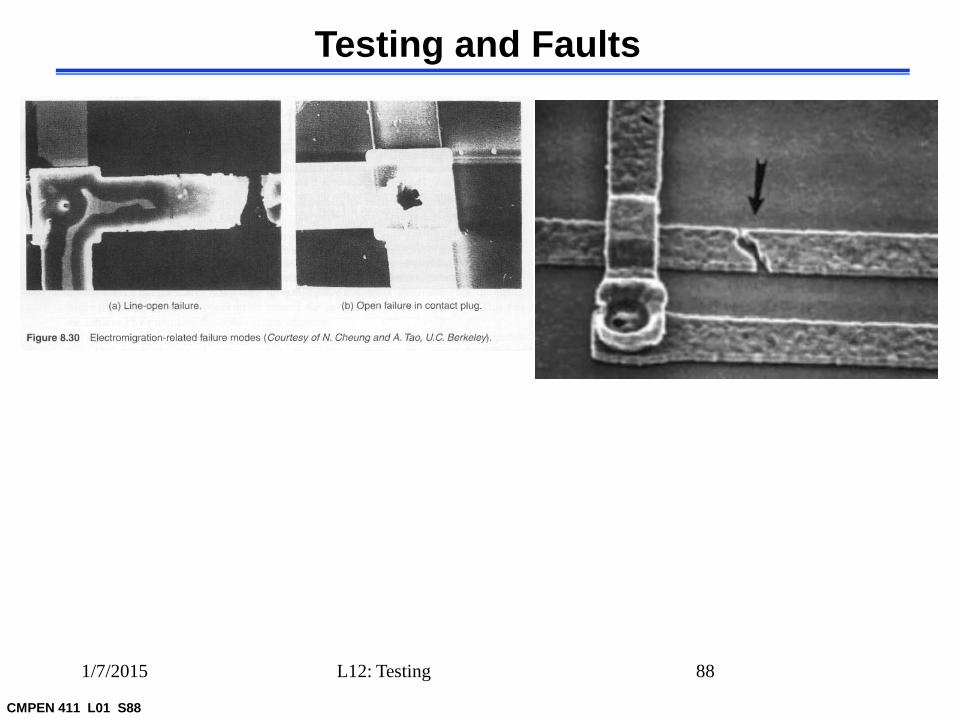
CMPEN 411 L01 S88
Testing and Faults
1/7/2015 88L12: Testing

CMPEN 411 L01 S89
Testing and Faults
1/7/2015 89L12: Testing

CMPEN 411 L01 S90
Testing and Faults
1/7/2015 90L12: Testing
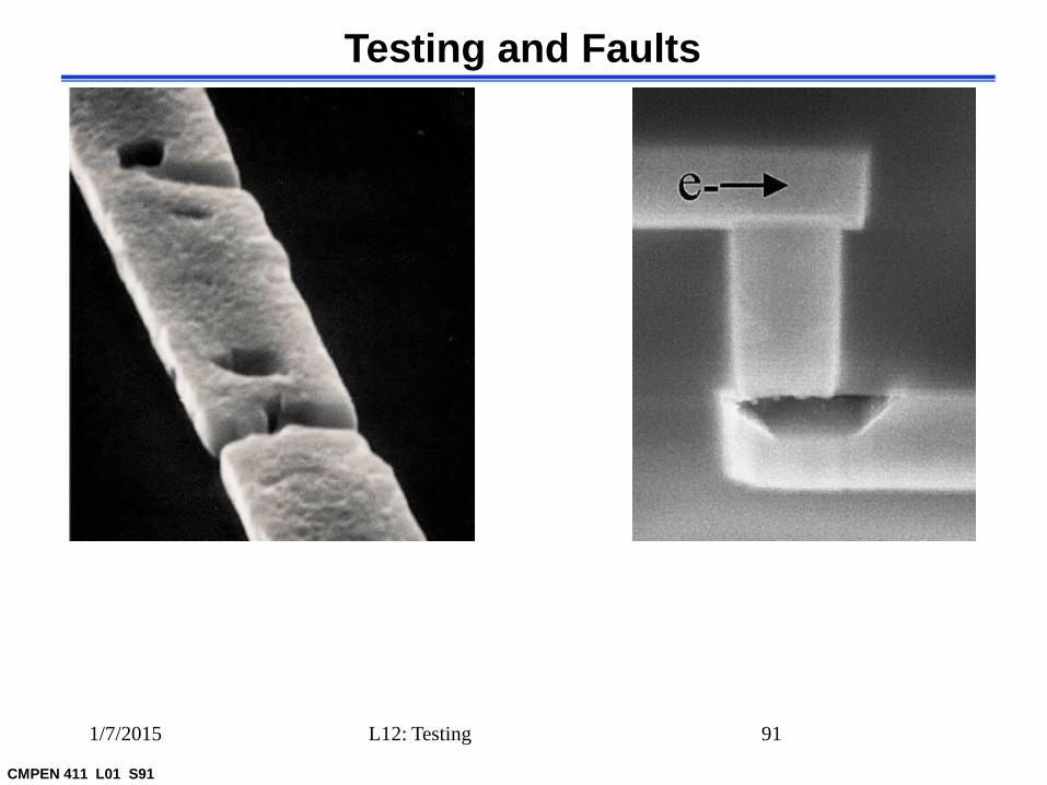
CMPEN 411 L01 S91
Testing and Faults
1/7/2015 91L12: Testing
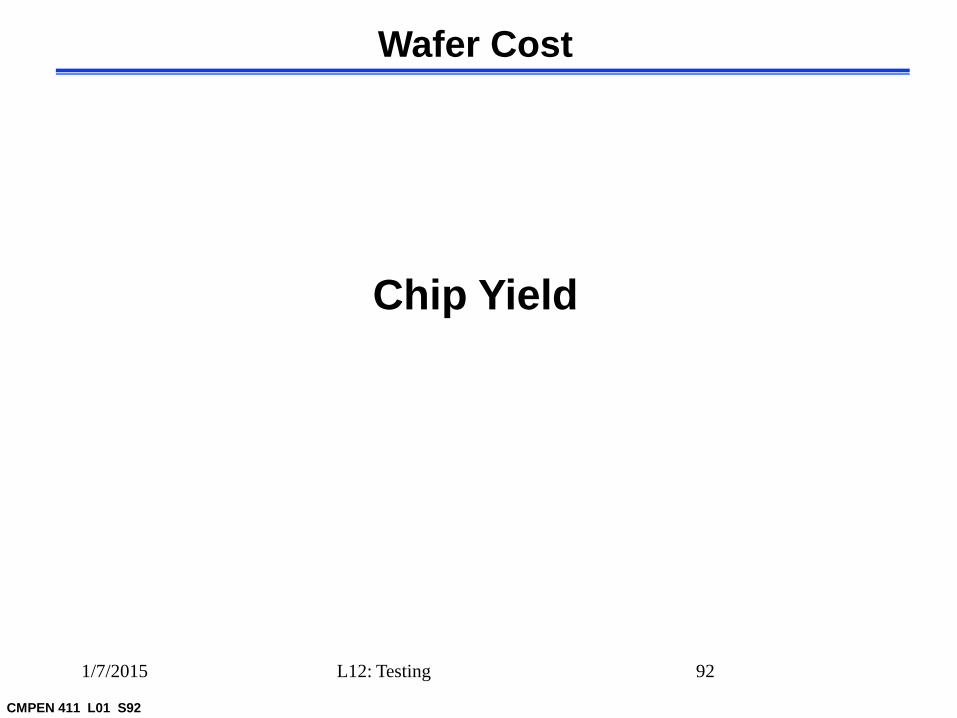
CMPEN 411 L01 S92
Wafer Cost
1/7/2015 92L12: Testing
Chip Yield

CMPEN 411 L01 S93
Testing and Faults
1/7/2015 93L12: Testing
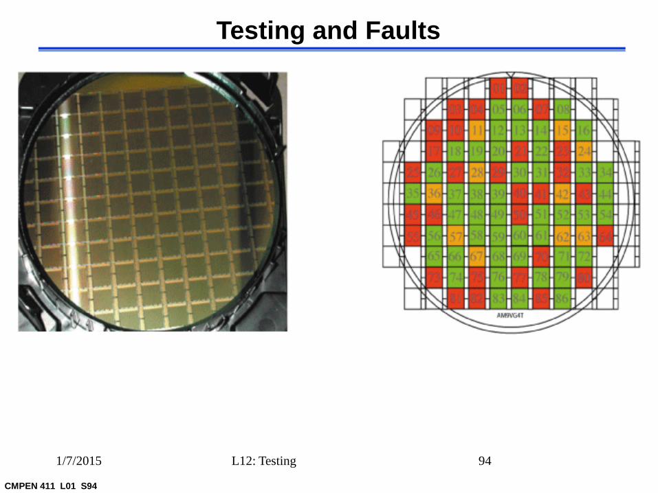
CMPEN 411 L01 S94
Testing and Faults
1/7/2015 94L12: Testing
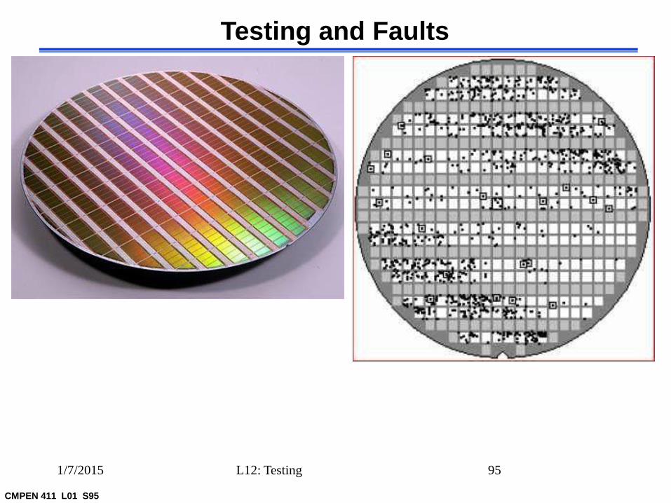
CMPEN 411 L01 S95
Testing and Faults
1/7/2015 95L12: Testing

CMPEN 411 L01 S96
Testing and Faults
1/7/2015 96L12: Testing
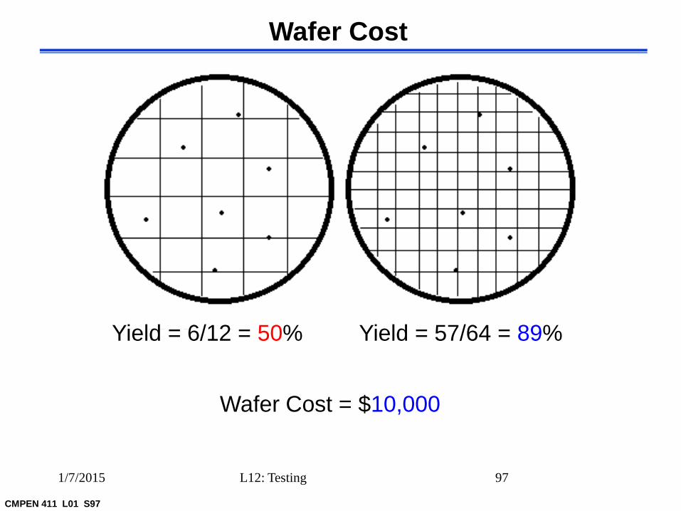
CMPEN 411 L01 S97
Wafer Cost
1/7/2015 97L12: Testing
Yield = 6/12 = 50% Yield = 57/64 = 89%
Wafer Cost = $10,000

CMPEN 411 L01 S98
Wafer Cost
1/7/2015 98L12: Testing

CMPEN 411 L01 S99
1/7/2015 99L12: Testing
Wafer Cost

CMPEN 411 L01 S100
1/7/2015 100L12: Testing
Wafer Cost

CMPEN 411 L01 S101
1/7/2015 101L12: Testing
Wafer Cost

CMPEN 411 L01 S102
1/7/2015 102L12: Testing
Wafer Cost

CMPEN 411 L01 S103
1/7/2015 103L12: Testing
Wafer Cost

CMPEN 411 L01 S104
Testing and Faults
1/7/2015 104L12: Testing
Fault Cost:
Wafer $0.01 - $ 0.1
Packaged Chip $0.1 - $1
Board $1 - $10
System $10 – 100
Field $100 - $1000

CMPEN 411 L01 S105
Testing and Faults
1/7/2015 105L12: Testing
Pentium Bug:
824 633 702 441.0 X 1/ 824 633 702 441.0
= 0.999 999 996 274 709 702
Due to faulty floating point number divide look-up table

CMPEN 411 L01 S106
Next Lecture and Reminders
Next lecture
Design metrics
- Reading assignment – 1.3
Reminders
Top Related