


Languages
Pages
Legal


EE 261 James Morizio 1
MOS Transistors
• Silicon substrate doped with impurities• Adding or cutting away insulating glass (SiO2)• Adding wires made of polycrystalline silicon (polysilicon,
poly) or metal, insulated from the substrate by SiO2
Drain Source
Gate
nn
Drain Source
Gate SiO2 (insulator)
p-type (doped)substrate
Drain Source
Gate
nMOS transistor
pMOS transistor
channel
Width WLength
L
Conductor(poly)

EE 261 James Morizio 2
Silicon Lattice• Transistors are built on a silicon substrate• Silicon is a Group IV material• Forms crystal lattice with bonds to four neighbors
Si SiSi
Si SiSi
Si SiSi

EE 261 James Morizio 3
Dopants• Silicon is a semiconductor• Pure silicon has no free carriers and conducts poorly• Adding dopants increases the conductivity• Group V: extra electron (n-type)• Group III: missing electron, called hole (p-type)
As SiSi
Si SiSi
Si SiSi
B SiSi
Si SiSi
Si SiSi
-
+
+
-

EE 261 James Morizio 4
p-n Junctions• A junction between p-type and n-type
semiconductor forms a diode.• Current flows only in one direction
p-type n-type
anode cathode

EE 261 James Morizio 5
nMOS Transistor• Four terminals: gate, source, drain, body• Gate – oxide – body stack looks like a capacitor
– Gate and body are conductors– SiO2 (oxide) is a very good insulator– Called metal – oxide – semiconductor (MOS) capacitor– Even though gate is
no longer made of metal
n+
p
GateSource Drain
bulk Si
SiO2
Polysilicon
n+

EE 261 James Morizio 6
nMOS Operation• Body is commonly tied to ground (0 V)• When the gate is at a low voltage:
– P-type body is at low voltage– Source-body and drain-body diodes are OFF– No current flows, transistor is OFF
n+
p
GateSource Drain
bulk Si
SiO2
Polysilicon
n+D
0
S

EE 261 James Morizio 7
nMOS Operation Cont.• When the gate is at a high voltage:
– Positive charge on gate of MOS capacitor– Negative charge attracted to body– Inverts a channel under gate to n-type– Now current can flow through n-type silicon from
source through channel to drain, transistor is ON
n+
p
GateSource Drain
bulk Si
SiO2
Polysilicon
n+D
1
S

EE 261 James Morizio 8
pMOS Transistor• Similar, but doping and voltages reversed
– Body tied to high voltage (VDD)– Gate low: transistor ON– Gate high: transistor OFF– Bubble indicates inverted behavior
SiO2
n
GateSource Drain
bulk Si
Polysilicon
p+ p+
EE 261 James Morizio 9
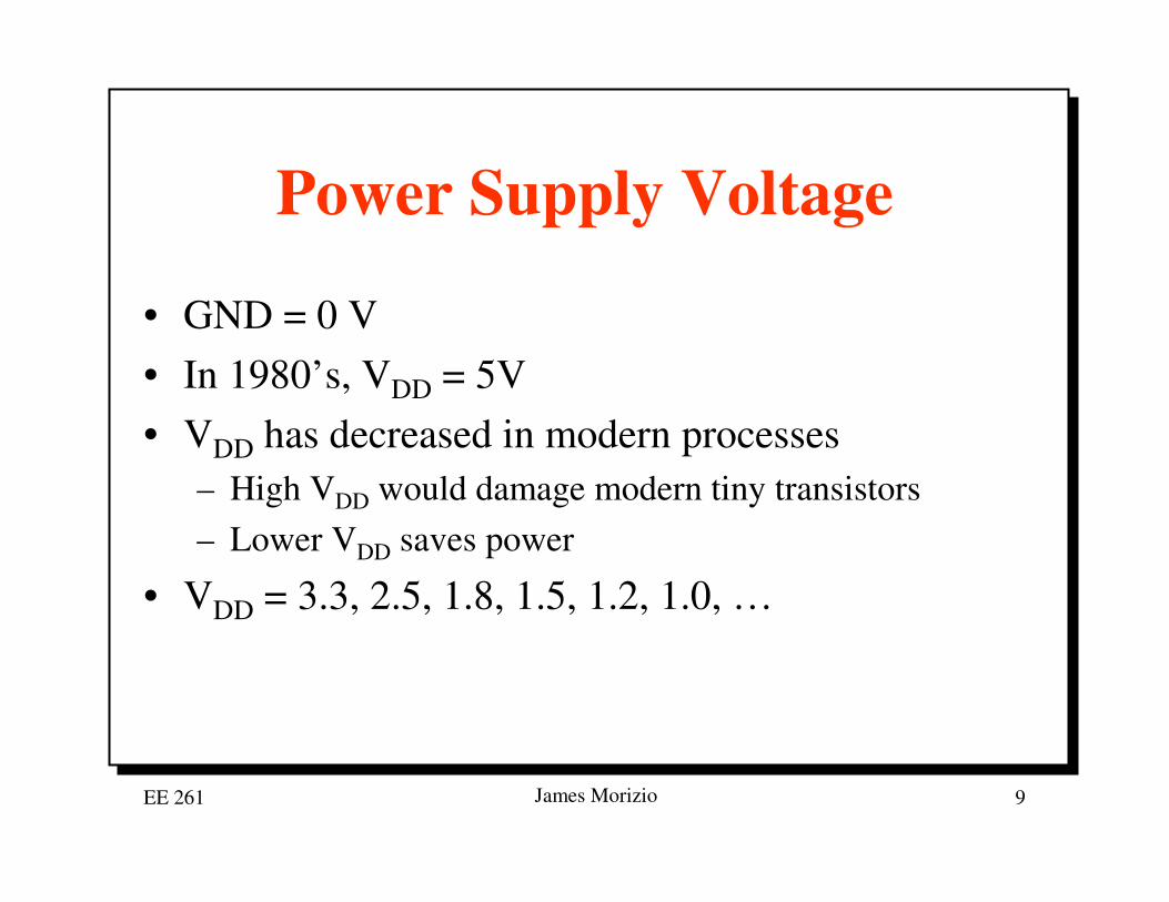
Power Supply Voltage
• GND = 0 V• In 1980’s, VDD = 5V• VDD has decreased in modern processes
– High VDD would damage modern tiny transistors– Lower VDD saves power
• VDD = 3.3, 2.5, 1.8, 1.5, 1.2, 1.0, …

EE 261 James Morizio 10
Transistors as Switches• We can view MOS transistors as electrically
controlled switches• Voltage at gate controls path from source to drain
g
s
d
g = 0
s
d
g = 1
s
d
g
s
d
s
d
s
d
nMOS
pMOS
OFF ON
ON OFF

EE 261 James Morizio 11
MOS Transistor Switches
N
a
b
s
N-switch a
b
sS = 0
S = 1
Good 0, Poor 1
0
1
0
1(degraded)

EE 261 James Morizio 12
MOS Transistor Switches
P-switcha
b
s P
a
b
s
S = 1
S = 0
Good 1, Poor 0
1
0
1
0(degraded)
a b
s
s
CMOS switch
a b
s
C S = 0
S = 1
a
Good 0Good 1
(Transmissiongate)
b
s
s

EE 261 James Morizio 13
Signal Strength
• Strength of signal– How close it approximates ideal voltage source
• VDD and GND rails are strongest 1 and 0• nMOS pass strong 0
– But degraded or weak 1
• pMOS pass strong 1– But degraded or weak 0
• Thus nMOS are best for pull-down network

EE 261 James Morizio 14
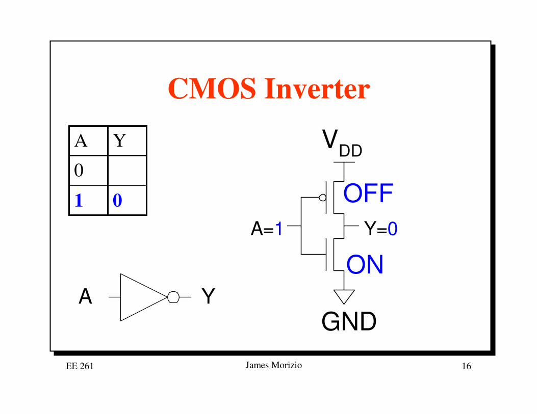
CMOS Inverter
1
0
YA VDD
A Y
GNDA Y

EE 261 James Morizio 15
CMOS Logic Gates-1Inverter
Input Outputa a
VDD
Gnd
Pull-down
Pull-up
path
path
2-input NAND
Gnd
VDD
a
b
a b
Pull-down
Pull-up
tree
tree
a b
z
z0 0 Z0 1 Z1 0 Z1 1 0
a b z0 0 10 1 11 0 11 1 Z
Pull-down Pull-uptruth tabletruth table
a b z0 0 10 1 11 0 11 1 0
NANDtruth table
EE 261 James Morizio 16
CMOS Inverter
010
YA VDD
A=1 Y=0
GND
ON
OFF
A Y

EE 261 James Morizio 17
CMOS Inverter
01
10YA VDD
A=0 Y=1
GND
OFF
ON
A Y

EE 261 James Morizio 18
CMOS NAND Gate
1
1
0
0
A
1
0
1
0
YB
A
B
Y

EE 261 James Morizio 19
CMOS NAND Gate
1
1
0
0A
1
0
1
10YB
A=0
B=0
Y=1OFF
ON ON
OFF

EE 261 James Morizio 20
CMOS NAND Gate
1
1
00
A
110
1
10
YB
A=0
B=1
Y=1OFF
OFF ON
ON

EE 261 James Morizio 21
CMOS NAND Gate
1
10
0
A
11
101
10
YB
A=1
B=0
Y=1ON
ON OFF
OFF

EE 261 James Morizio 22
CMOS NAND Gate
11
0
0
A
11
10
01
10
YB
A=1
B=1
Y=0ON
OFF OFF
ON

EE 261 James Morizio 23
CMOS NOR Gate
1
1
0
0
A
01
00
01
10
YB
A
BY

EE 261 James Morizio 24
CMOS Logic Gates-22-input NOR
Gnd
VDD
a b
a
b
Pull-down
Pull-up
tree
tree
a b
z
z0 0 Z0 1 01 0 01 1 0
a b z0 0 10 1 Z1 0 Z1 1 Z
Pull-down Pull-uptruth tabletruth table
a b z0 0 10 1 01 0 01 1 0
NORtruth table
• Generalize to n-input NAND and n-input NOR?
• There is always (for all input combinations) a pathfrom either 1 or 0 to the output
• No direct path from 1 to 0 (low power dissipation)• Fully restored logic• No ratio-ing is necessary (ratio-less logic)
EE 261 James Morizio 25
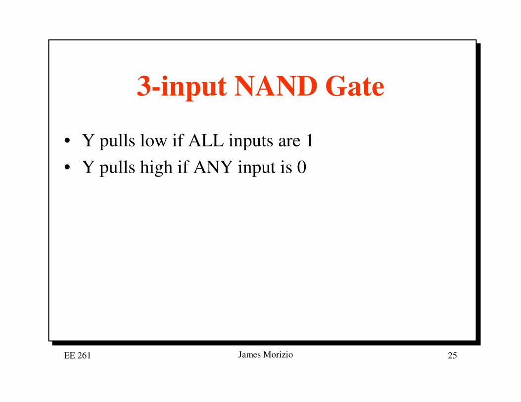
3-input NAND Gate
• Y pulls low if ALL inputs are 1• Y pulls high if ANY input is 0

EE 261 James Morizio 26
3-input NAND Gate• Y pulls low if ALL inputs are 1• Y pulls high if ANY input is 0
A
B
Y
C

EE 261 James Morizio 27
CMOS Compound (Complex) Gates-1
• What function is implemented by this circuit?
z
c d
Gnd
a
b
VDD
a b c
d

EE 261 James Morizio 28
Compound Gates-2VDD
a
b
a
How to implementF = ab + bc + ca?
• F = ab + bc + ca
b
ac
c
b
a b
VDD
Gnd
F F
Gnd
c
c

EE 261 James Morizio 29
And-Or-Invert (AOI) Gatesabc
de
fgh
F
Pull-upnetwork
a
b
c
F
Gnd
h
f
g
d
e

EE 261 James Morizio 30
Or-And-Invert (OAI) Gate
abc
de
fgh
Fa b c
Pull-upnetwork
d e
f g h
Gnd
F
• Generally, complex CMOS gates can be derived directly from maxterms of thefunction (as in a Karnaugh map)

EE 261 James Morizio 31
Transmission Gates
• Pass transistors produce degraded outputs• Transmission gates pass both 0 and 1 well

EE 261 James Morizio 32
Transmission Gates• Pass transistors produce degraded outputs• Transmission gates pass both 0 and 1 well
g = 0, gb = 1a b
g = 1, gb = 0a b
0 strong 0
Input Output
1 strong 1
g
gb
a b
a bg
gb
a b
g
gb
a b
g
gb
g = 1, gb = 0
g = 1, gb = 0

EE 261 James Morizio 33
Tristates
• Tristate buffer produces Z when not enabled
11011000
YAENA Y
EN
A Y
EN
EN

EE 261 James Morizio 34
Tristates• Tristate buffer produces Z when not enabled
111001Z10Z00YAEN
A Y
EN
A Y
EN
EN

EE 261 James Morizio 35
Nonrestoring Tristate• Transmission gate acts as tristate buffer
– Only two transistors– But nonrestoring
• Noise on A is passed on to Y
A Y
EN
EN
EE 261 James Morizio 36
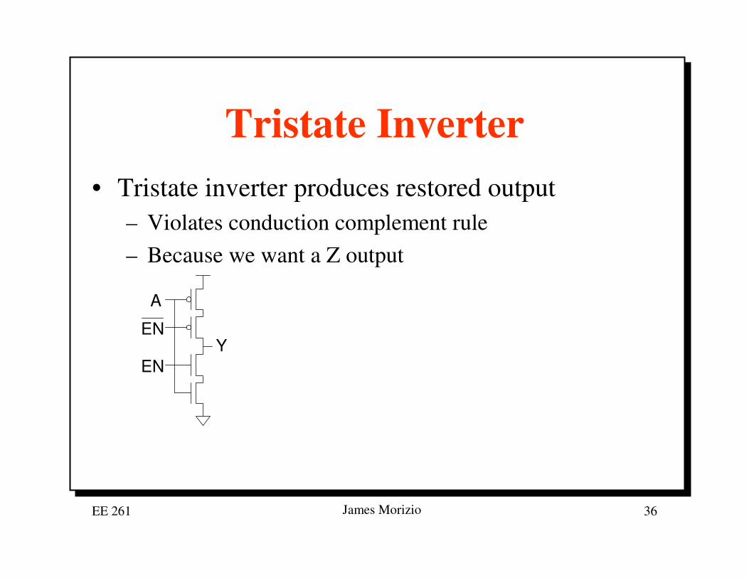
Tristate Inverter• Tristate inverter produces restored output
– Violates conduction complement rule– Because we want a Z output
A
YEN
EN

EE 261 James Morizio 37
Tristate Inverter• Tristate inverter produces restored output
– Violates conduction complement rule– Because we want a Z output
A
YEN
A
Y
EN = 0Y = 'Z'
Y
EN = 1Y = A
A
EN

EE 261 James Morizio 38
Multiplexers
• 2:1 multiplexer chooses between two inputs
X11X011X00X0
YD0D1S0
1
S
D0
D1Y

EE 261 James Morizio 39
Multiplexers
• 2:1 multiplexer chooses between two inputs
1X110X0111X000X0YD0D1S
0
1
S
D0
D1Y

EE 261 James Morizio 40
Gate-Level Mux Design
• How many transistors are needed?
1 0 (too many transistors)Y SD SD= +

EE 261 James Morizio 41
Gate-Level Mux Design• How many transistors are needed? 20
1 0 (too many transistors)Y SD SD= +
44
D1
D0S Y
4
2
22 Y
2
D1
D0S

EE 261 James Morizio 42
Transmission Gate Mux
• Nonrestoring mux uses two transmission gates

EE 261 James Morizio 43
Transmission Gate Mux
• Nonrestoring mux uses two transmission gates– Only 4 transistors S
S
D0
D1
YS

EE 261 James Morizio 44
Inverting Mux• Inverting multiplexer
– Use compound AOI22– Or pair of tristate inverters– Essentially the same thing
• Noninverting multiplexer adds an inverter
S
D0 D1
Y
S
D0
D1Y
0
1S
Y
D0
D1
S
S
S
S
S
S

EE 261 James Morizio 45
4:1 Multiplexer
• 4:1 mux chooses one of 4 inputs using two selects

EE 261 James Morizio 46
4:1 Multiplexer
• 4:1 mux chooses one of 4 inputs using two selects– Two levels of 2:1 muxes– Or four tristates
S0
D0
D1
0
1
0
1
0
1Y
S1
D2
D3
D0
D1
D2
D3
Y
S1S0 S1S0 S1S0 S1S0

EE 261 James Morizio 47
CMOS Exclusive-Nor Gatea
b
F = a b
• 8-transistor implementation
TG1
TG2
a b TG1 TG2 F
0 0 nonconducting conducting B (1)0 1 nonconducting conducting B (0)1 0 conducting nonconducting B (0)1 1 conducting nonconducting B (1)
• Better, 6-transistor implementation is possible!

EE 261 James Morizio 48
D Latch• When CLK = 1, latch is transparent
– D flows through to Q like a buffer
• When CLK = 0, the latch is opaque– Q holds its old value independent of D
• a.k.a. transparent latch or level-sensitive latch
CLK
D Q
Latc
h D
CLK
Q

EE 261 James Morizio 49
D Latch Design• Multiplexer chooses D or old Q
1
0
D
CLK
QCLK
CLKCLK
CLK
DQ Q
Q

EE 261 James Morizio 50
D Latch Operation
CLK = 1
D Q
Q
CLK = 0
D Q
Q
D
CLK
Q

EE 261 James Morizio 51
D Flip-flop
• When CLK rises, D is copied to Q• At all other times, Q holds its value• a.k.a. positive edge-triggered flip-flop, master-
slave flip-flop
Flop
CLK
D Q
D
CLK
Q

EE 261 James Morizio 52
D Flip-flop Design
• Built from master and slave D latches
QM
CLK
CLKCLK
CLK
Q
CLK
CLK
CLK
CLK
D
Latc
h
Latc
h
D QQM
CLK
CLK

EE 261 James Morizio 53
D Flip-flop Operation
CLK = 1
D
CLK = 0
Q
D
QM
QMQ
D
CLK
Q

EE 261 James Morizio 54
Race Condition• Back-to-back flops can malfunction from clock
skew– Second flip-flop fires late– Sees first flip-flop change and captures its result– Called hold-time failure or race condition
CLK1
D Q1
Flop
Flop
CLK2
Q2
CLK1
CLK2
Q1
Q2

EE 261 James Morizio 55
Nonoverlapping Clocks• Nonoverlapping clocks can prevent races
– As long as nonoverlap exceeds clock skew
• We will use them in this class for safe design– Industry manages skew more carefully instead
φ1
φ1φ1
φ1
φ2
φ2φ2
φ2
φ2
φ1
QMQD

EE 261 James Morizio 56
Design Representation Levels• Design domains
– Behavioral– Structural– Physical
Gajski and Kuhn’s Y-chart(layered like an onion)
Behavioral Structural
Physical (geometric)
Chip
Cells
Polygons
TransistorsGates
ProcessorBoolean equationsDifferential equations
Algorithms
• Hardware description languages commonly used at behavioral level, e.g. VHDL, Verilog
• Example: Consider the carry function co = ab + bc + cia
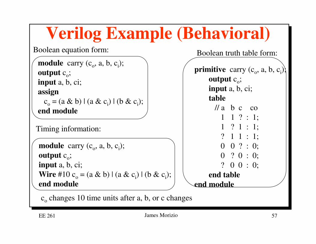
EE 261 James Morizio 57
Verilog Example (Behavioral)module carry (co, a, b, ci);output co;input a, b, ci;assign
co = (a & b) | (a & ci) | (b & ci);end module
Boolean equation form: Boolean truth table form:
primitive carry (co, a, b, ci);output co;input a, b, ci;table
// a b c co1 1 ? : 1;1 ? 1 : 1;? 1 1 : 1;0 0 ? : 0;0 ? 0 : 0;? 0 0 : 0;
end tableend module
Timing information:
module carry (co, a, b, ci);output co;input a, b, ci;Wire #10 co = (a & b) | (a & ci) | (b & ci);end module
co changes 10 time units after a, b, or c changes

EE 261 James Morizio 58
Verilog Example (Structural)
module add4 (s, c4, ci, a, b);output [3:0] s;output [3:0] c4;input [3:0] a, b;input ci;wire [2:0] co;
add a0 (co[0], s[0], a[0], b[0], ci);add a1 (co[1], …, b[1], co[0]);add a2 (co[2], …, , co[1]);add a3 (c4, s[3], a[3], b[3], co[2]);
end module
Structural representation of 4-bit adder (top-down) :module add (co, s, a, b, ci);
output s, co;input a, b, ci;sum s1 (s, a, b, ci);carry c1 (co, a, b, ci);
end module
internal3-bit
signal
module carry (co, a, b, ci);output co;input a, b, ci;wire x, y, z;and g1 (y, z, b);and g2 (z, b, ci);and g3 (z, a, ci);or g4 (co, x, y, z);
end moduleTechnology-independent
Top Related